EP2941639B1 - Dreidimensionale, dispergierbare nanoresonator-struktur für biologische, medizinische und umwelttechnische anwendungen und verfahren zur herstellung derselben - Google Patents
Dreidimensionale, dispergierbare nanoresonator-struktur für biologische, medizinische und umwelttechnische anwendungen und verfahren zur herstellung derselben Download PDFInfo
- Publication number
- EP2941639B1 EP2941639B1 EP13831876.1A EP13831876A EP2941639B1 EP 2941639 B1 EP2941639 B1 EP 2941639B1 EP 13831876 A EP13831876 A EP 13831876A EP 2941639 B1 EP2941639 B1 EP 2941639B1
- Authority
- EP
- European Patent Office
- Prior art keywords
- layer
- nanoresonators
- nanoresonator
- conductive material
- substrate
- Prior art date
- Legal status (The legal status is an assumption and is not a legal conclusion. Google has not performed a legal analysis and makes no representation as to the accuracy of the status listed.)
- Active
Links
Images




Classifications
-
- B—PERFORMING OPERATIONS; TRANSPORTING
- B82—NANOTECHNOLOGY
- B82Y—SPECIFIC USES OR APPLICATIONS OF NANOSTRUCTURES; MEASUREMENT OR ANALYSIS OF NANOSTRUCTURES; MANUFACTURE OR TREATMENT OF NANOSTRUCTURES
- B82Y30/00—Nanotechnology for materials or surface science, e.g. nanocomposites
-
- G—PHYSICS
- G01—MEASURING; TESTING
- G01N—INVESTIGATING OR ANALYSING MATERIALS BY DETERMINING THEIR CHEMICAL OR PHYSICAL PROPERTIES
- G01N21/00—Investigating or analysing materials by the use of optical means, i.e. using sub-millimetre waves, infrared, visible or ultraviolet light
- G01N21/17—Systems in which incident light is modified in accordance with the properties of the material investigated
- G01N21/25—Colour; Spectral properties, i.e. comparison of effect of material on the light at two or more different wavelengths or wavelength bands
- G01N21/31—Investigating relative effect of material at wavelengths characteristic of specific elements or molecules, e.g. atomic absorption spectrometry
- G01N21/35—Investigating relative effect of material at wavelengths characteristic of specific elements or molecules, e.g. atomic absorption spectrometry using infrared light
- G01N21/3581—Investigating relative effect of material at wavelengths characteristic of specific elements or molecules, e.g. atomic absorption spectrometry using infrared light using far infrared light; using Terahertz radiation
-
- G—PHYSICS
- G01—MEASURING; TESTING
- G01N—INVESTIGATING OR ANALYSING MATERIALS BY DETERMINING THEIR CHEMICAL OR PHYSICAL PROPERTIES
- G01N29/00—Investigating or analysing materials by the use of ultrasonic, sonic or infrasonic waves; Visualisation of the interior of objects by transmitting ultrasonic or sonic waves through the object
- G01N29/02—Analysing fluids
- G01N29/036—Analysing fluids by measuring frequency or resonance of acoustic waves
-
- G—PHYSICS
- G01—MEASURING; TESTING
- G01N—INVESTIGATING OR ANALYSING MATERIALS BY DETERMINING THEIR CHEMICAL OR PHYSICAL PROPERTIES
- G01N29/00—Investigating or analysing materials by the use of ultrasonic, sonic or infrasonic waves; Visualisation of the interior of objects by transmitting ultrasonic or sonic waves through the object
- G01N29/22—Details, e.g. general constructional or apparatus details
- G01N29/24—Probes
- G01N29/2418—Probes using optoacoustic interaction with the material, e.g. laser radiation, photoacoustics
-
- G—PHYSICS
- G01—MEASURING; TESTING
- G01N—INVESTIGATING OR ANALYSING MATERIALS BY DETERMINING THEIR CHEMICAL OR PHYSICAL PROPERTIES
- G01N2291/00—Indexing codes associated with group G01N29/00
- G01N2291/02—Indexing codes associated with the analysed material
- G01N2291/024—Mixtures
- G01N2291/02466—Biological material, e.g. blood
-
- G—PHYSICS
- G01—MEASURING; TESTING
- G01N—INVESTIGATING OR ANALYSING MATERIALS BY DETERMINING THEIR CHEMICAL OR PHYSICAL PROPERTIES
- G01N2291/00—Indexing codes associated with group G01N29/00
- G01N2291/02—Indexing codes associated with the analysed material
- G01N2291/025—Change of phase or condition
- G01N2291/0255—(Bio)chemical reactions, e.g. on biosensors
-
- G—PHYSICS
- G01—MEASURING; TESTING
- G01N—INVESTIGATING OR ANALYSING MATERIALS BY DETERMINING THEIR CHEMICAL OR PHYSICAL PROPERTIES
- G01N2291/00—Indexing codes associated with group G01N29/00
- G01N2291/02—Indexing codes associated with the analysed material
- G01N2291/025—Change of phase or condition
- G01N2291/0256—Adsorption, desorption, surface mass change, e.g. on biosensors
- G01N2291/0257—Adsorption, desorption, surface mass change, e.g. on biosensors with a layer containing at least one organic compound
Definitions
- the present invention relates to nanosensors, in particular nanosensors for biological, medical and environmental applications, and more specifically a three-dimensional nanoresonator structure.
- the invention also relates to a method for the manufacture, by lithographic techniques, of three-dimensional nanoresonators that are dispersible in a liquid such as water.
- Nanoresonators also known as nanoantennas, are resonator devices of nanometric dimensions which, when exposed to wide-spectrum exciting electromagnetic radiation, show increased absorption at a natural resonant frequency determined by the characteristics of the resonator structure and/or by the interactions with the environment in which they are immersed, this frequency being located between the THz range and the near infrared wavelengths.
- nanoresonators Two classes of nanoresonators, namely structured nanoresonators and nanoparticles with resonant properties, are known in the prior art.
- Structured nanoresonators may be described as nanometric-scale circuits, the resonant properties of which are determined by the inductance and capacitance characteristics of the circuit, and are therefore also known as LC metamaterials.
- Metamaterials have characteristic properties which depend on the geometry of the device, instead of on its chemical composition.
- the most common structured nanoresonators are based on a two-dimensional open-loop configuration, such as that shown in Figure 1 together with an equivalent electrical circuit.
- This two-dimensional nanoresonator structure comprises a conductive metal microstrip (typically made of gold) shaped to form an open loop, in which, at the operating frequencies of the device, the loop-shaped path shows distributed inductive behaviour and the gap in the ring acts as a capacitor.
- Nanoresonators of this type have an intrinsically two-dimensional structure, which has to be supported on the surface of a substrate from which, therefore, they cannot be separated.
- the resonance of these devices can be tuned over a wide range of wavelengths, by suitable design of the resonance structure, but their use is limited by the dimensions of the array and by the nature of the substrate to which they are anchored.
- WO 2011/050272 describes an array of two-dimensional nanoantennas and processes for the efficient manufacture of an array of nanoantennas whose shape is controlled by nanostencil lithography. This method can be used to produce nanoresonator structures on virtually any type of support, whether conductive, non-conductive or magnetic, with properties of flexibility and stretchability if required.
- the array of nanoantennas formed in this way can be used in spectrometry, for the detection of bioanalytes or inorganic chemical substances having resonant frequencies in the infrared range.
- the circuit includes an array of resonators operating at THz frequencies, each comprising a first metal electrode anchored to a substrate, an intermediate non-conductive polymer layer, and a second conductive metal electrode for functionalization, adapted to bind DNA strands. These resonators are used to detect the presence of molecules which bind to the functionalized surface, making use of the fact that their resonance properties vary as a function of the presence of these molecular bonds.
- nanoresonators Unlike structured nanoresonators, some free metallic nanoparticles, which can be produced by chemical synthesis, are known to act as nanoresonators because of the resonance of the plasmon waves which are established on the surfaces of the molecules.
- nanoparticles of Ag:SiO 2 and Au:SiO 2 in colloidal suspension have been used as electromagnetic nanoresonators, as described by A. Kudelski and S. Wojtysiak, in "Silica-Covered Silver and Gold Nanoresonators for Raman Analysis of Surfaces of Various Materials", published in J. Phys. Chem. C. 2012, 116 (30), pages 16167-16174 .
- resonant nanoparticles not bound to any substrate, can be dispersed freely in a fluid medium and can be used advantageously for in vivo applications, by exploiting, where appropriate, their capacity to bind to molecular species present in the fluid medium, which affect their resonance properties.
- the resonance properties are mainly determined by the intrinsic characteristics of the material of the nanoparticles, and since the chemical synthesis process does not enable complexes of nanoparticles to be produced with controlled shapes, the resonance can only be tuned over a limited range of wavelengths.
- US 2003/0166297 discloses surface enhanced spectroscopy-active composite nanoparticles used as submicron-sized tags or labels that can be covalently or non-covalently affixed to entities of interest for the purpose of quantification, location, identification, or tracking.
- the object of the present invention is to provide three-dimensional nanoresonators which are free, that is to say not fixed to any substrate and dispersible in a fluid medium, and have resonance properties tunable over a wide spectrum of wavelengths as a result of the design of the resonant structure, while being sensitive to the chemical and physical characteristics of their environment or to the presence of specific molecular species. According to the present invention, this object is achieved by means of a three-dimensional nanoresonator structure having the characteristics claimed in Claim 1.
- the invention also proposes a method for the manufacture of three-dimensional nanoresonators as claimed.
- the present invention is based on a technique of manufacturing three-dimensional nanoresonators by a lithographic procedure in which an array of nanoresonators is designed and manufactured on a substrate and the individual nanoresonators are subsequently released from the substrate, and subjected to chemical modification if necessary, for the functionalization of at least one accessible surface exposed to environmental interactions.
- the nanoresonators proposed by the invention have an overall layered three-dimensional structure, with layers of different materials, the shape and size of which can be controlled in the design process.
- the innovative three-dimensional structure of nanoresonators that can be produced by the method proposed by the invention has a plurality of accessible surfaces, that is to say surfaces exposed to the environment, made of different materials suitable for separate functionalization, thus enhancing the sensing functions of the device.
- the functionalization may be such that it allows a free dispersion of the nanoresonators in water or other fluid media, and makes it possible to produce probes sensitive to predetermined molecular interactions, or it may be such that it creates affinities for specific tissues, cells or materials to be analysed.
- the nanoresonators produced according to the present invention have characteristics which significantly extend their range of applications, by combining the properties of design flexibility of the resonant frequency over a wide electromagnetic spectrum, typical of prior art two-dimensional nanoresonators, with the dispersibility properties of resonant nanoparticles.
- Nanoresonators operating in the near infrared region can be used for diagnostic applications on living creatures, since the absorption of the tissues in this spectral range is fairly low (the "biological window"), while nanoresonators operating at THz frequencies can be used to study materials transparent in this region of the electromagnetic spectrum, for example some polymers such as polymethylpentene, polypropylene or polyethylene.
- the intrinsically three-dimensional structure of the nanoresonator proposed by the invention has considerable advantages over a two-dimensional nanoresonator structure. This is because the compact three-dimensional structure is capable of being freely self-supporting, with no support by a substrate, without any appreciable changes in its shape and resonant frequency, as a result of which the nanoresonator proposed by the invention is dispersible in solution and is adapted to show stable behaviour based on the controlled design of its intrinsic resonant frequency.
- the nanoresonators can be injected into a living organism for in vivo analysis as a diagnostic means, or for detecting physiological or biochemical events, or for use in fluid or microfluid assays in which the fluid medium of immersion affects the overall dielectric constant of the resonant circuit, or for impregnating porous materials such as marble or stone used for works of art in investigative and diagnostic operations conducted on cultural assets.
- Nanoresonators suspended in a liquid phase can also be conjugated with functional groups to bind to specific tissues or cells to be analysed.
- the nanoresonator 10 has a generally prismatic structure and comprises a stack of superimposed layers of uniform dimensions, these layers being, respectively, a first electrode layer 12 of conductive material, preferably made of metal and even more preferably made of aluminium, an intermediate layer 14 of dielectric material, preferably an aluminium oxide, and a second electrode layer 16 of conductive material, preferably made of metal and different from the conductive material of the first electrode layer, and even more preferably made of gold.
- nanoresonators of prismatic shape, having a polygonal or circular cross section, or of any arbitrarily chosen shape; or it is possible to make stacked structures in which the transverse extension and depth of each layer are different from those of the other layers, each of these dimensions and materials contributing to the design of the resonant frequency of the overall structure.
- nanoresonator structures comprising more than three layers are possible, while it is also possible to make structures containing connection elements (shunts) between non-adjacent conductive layers, so that the electromagnetic resonance properties of the nanoresonator can be controlled electrically, rather than purely geometrically.
- the choice of different materials for the electrode layers 12, 16 of the nanoresonator plays an important part in the process of manufacturing the nanoresonator, as will be made clear by the remainder of this description, since it allows the nanoresonator structure to be separated, in a process of lithographic definition of the structure of the device, from a sacrificial forming substrate on which it is deposited and configured in a predetermined designed layout.
- the prismatic structure of the nanoresonator 10 has layers 12, 14 and 16 which are freely accessible and can be functionalized independently of each other, since they have at least one surface area, 12', 14' and 16' respectively, exposed to the environment.
- the surface areas 12', 14' and 16' exposed to the environment coincide with at least the side surface of each layer, while the lower and upper bases 12", 16", respectively, of the electrode layers at the ends of the stack can also be exposed to the environment.
- the equivalent electrical circuit of the exemplary nanoresonator structure according to the invention is shown next to the three-dimensional representation of said structure. It consists of an LC resonant circuit, in which the inductive behaviour is determined by the antiparallel loop current propagated in the pair formed by the electrode layers, and the outer regions of the electrode layers, where the current causes an accumulation of opposing charges, act as the plates of a capacitor.
- a nanoresonator structure adapted to resonate in the near infrared range has dimensions of about 200 nm on its long side and 100 nm on its short side, and each layer has a thickness of 50 nm, making the nanoresonator arranged for use in biological applications.
- a nanoresonator adapted to resonate in the THz range has typical dimensions between 2 ⁇ m and 10 ⁇ m.
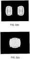
- Figure 2b shows the pattern of the lines of electric field intensity established on the nanoresonator
- Figure 2c shows the intensity pattern of the magnetic field lines established on the nanoresonator.
- the electric field is confined to the sides, at the smaller faces of the structure, while the magnetic field is concentrated around the central region of the structure; that is to say, the two ends of the nanoresonator exhibit capacitive behaviour and the central portion of the structure exhibits inductive behaviour.
- the manufacturing process which is itself inventive, includes three different macro steps, namely the manufacture of an array of nanoresonators on a supporting substrate by planar lithography, the separation of the nanoresonators from the substrate and the conjugation of the nanoresonators once they are free, in other words no longer rigidly fixed to the substrate, with chemical agents adapted to facilitate the formation of a stable colloidal suspension in a liquid medium.
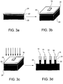
- this shows a gallium arsenide substrate 20 adapted to support the formation of an array of resonant nanostructures, on which a first conductive layer 22 of aluminium is deposited, by evaporation for example, so as to form a first electrode 12, and an intermediate layer 24 of aluminium oxide (Al 2 O 3 ) is also deposited, by known sputtering techniques for example, so as to form an intermediate dielectric 14 of the nanoresonator structure of Figure 2a .
- a gallium arsenide substrate 20 adapted to support the formation of an array of resonant nanostructures, on which a first conductive layer 22 of aluminium is deposited, by evaporation for example, so as to form a first electrode 12, and an intermediate layer 24 of aluminium oxide (Al 2 O 3 ) is also deposited, by known sputtering techniques for example, so as to form an intermediate dielectric 14 of the nanoresonator structure of Figure 2a .
- Figure 3b shows a subsequent step of lithography which is carried out by using an electronic beam to expose a commercial positive resist (ARP 67902), previously deposited by spin coating at 400 r.p.m. and baked at 170°C for 5 minutes.
- ARP 67902 commercial positive resist
- a second conductive layer of gold is deposited, so as to form a second electrode 16 of the nanoresonator structure.
- the evaporation of the gold is preceded by the deposition of a thin layer of chromium (5 nm). Additionally, the deposition of the gold is followed by the evaporation of a layer of nickel (10 nm) which is used as a mask for the dry etching.
- a dry etching step is then performed, using a technique of reactive ion etching through a reactive plasma (inductively coupled plasma) of BCl 3 , Cl 2 and Ar, to remove the first conductive layer of aluminium (layer 22) and the intermediate layer of aluminium oxide (layer 24) located thereon, with the use of the masking provided by the gold electrode pads 16; in other words, the removal takes place in the regions outside the stacked configuration of the nanoresonator structure.
- a reactive plasma inductively coupled plasma
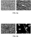
- Figure 4a shows a scanning electron microscope image of a regular array of nanoresonators fixed to a GaAs substrate, the nanoresonators being spaced one micron apart in both directions on the plane.
- Figure 4b shows an enlarged view of the image of Figure 4a .
- the nanoresonator structures are released from the substrate, although they continue to adhere weakly to it because of adhesion forces such as the Van der Waals force, in random positions, being tipped onto one side or inverted, for example.
- the result of this step is shown schematically in Figure 3f , where the solution (water, for example) has been removed under a vacuum, and scanning microscope images are reproduced in Figures 4c and 4d , showing an overall view and an enlarged view respectively.
- the nanoresonator structures which are now released from the substrate and are independent of each other, are then dispersed in a liquid medium 30. This process is facilitated by a fast sonication step (for 40 seconds) in a vessel containing N,N-dimethylformamide (DMF).
- a fast sonication step for 40 seconds
- a vessel containing N,N-dimethylformamide (DMF) for 40 seconds
- the nanoresonators are functionalized with APTES, which contributes ethoxysilane groups that react with hydroxylated surfaces such as the Al and Al 2 O 3 surfaces, causing the formation of Si-O-surface bonds with the exposed surface 14' of the intermediate layer 14 of dielectric material and with the exposed surfaces 12' and 12" of the first electrode layer 12 of conductive material. Since the surface of the second electrode layer 16 of gold, exposed to the environment, has no hydroxyl groups, only the exposed areas of the intermediate dielectric layer 14 of aluminium oxide and of the first electrode layer 12 of aluminium are functionalized.
- the reaction takes place when the nanoresonators are in suspension in N,N-dimethylformamide, after the sonication step described with reference to Figure 3g , after the addition of APTES modified with polyethylene glycol and acetic acid, which act as catalysts, at a reflux temperature for a period of 24 hours.
- the nanostructures functionalized in this way can be dispersed in water by sonication and purified by dialysis through a membrane, preferably with a cut-off of 10 kDa.
- the properties of resonance in the optical range of specimens of nanoresonators as proposed by the invention and manufactured by the inventors according to the inventive method were measured with a Nexus Fourier transform spectrometer fitted with a white light lamp and a lead selenide detector. Measurements of reflectance were made on an array of nanoresonators fixed to the manufacturing substrate, and on a collection of nanoresonators which were no longer fixed to the substrate in an ordered array, but had adhered to it in random positions and orientations.
- Figure 5a shows the result of the reflectance measurements for an array of nanoresonators on a substrate (as in Figure 4a ), and Figure 5b shows the results of the reflectance measurements for a collection of nanoresonators adhering to the substrate (as in Figure 4b ), in a condition of exposure to air (curve A) and in a condition of exposure to water (curve B) respectively.
- the resonance spectrum was calculated as the ratio between the spectrum of the nanoresonators and the spectrum of the substrate only.
- Figure 5b shows a measurable shift in the resonant frequency as a result of the different dielectric properties of the medium (air or water) in which the nanoresonators are immersed, which affects the determination of the overall capacitance viewed from the structure and ultimately affects the resonant frequency.
- a second set of experiments was conducted using a microfluidics device to make accurate measurements of the behaviour of the nanoresonators when immersed in a liquid environment.
- a test chamber having dimensions of about 200 x 200 x 30 ⁇ m, illuminated with a beam of light focused on a diameter in the range from 30 ⁇ m to 100 ⁇ m, the transmission spectra of the nanoresonators proposed by the invention were acquired in different conditions of immersion in the environment, that is to say in different dispersion environments of the nanoresonators.
- the inventors have also investigated the effects of the chemical bonds on the metallic surfaces of the nanoresonators (electrodes 12 and 16), by progressively exposing the nanoresonators to a solution of cysteamine diluted 1:1000 in water. It is known that cysteamine forms bonds with gold, in this case with the electrode 16 of the nanoresonator, forming a sulphur bridge and thereby affecting the optical properties of the nanoresonator.
- Figure 7 shows the time dependence of the optical transmission curves of the nanoresonators proposed by the invention in the presence of cysteamine.
- a shift in resonance wavelength of about 50 nm is observable between the condition in which the nanoresonators are free of bonds (the condition in which cysteamine is absent, shown by curve A) and the condition in which the nanoresonators are functionalized with bonds to cysteamine (after a period of 30 minutes of exposure to cysteamine in solution, shown by curve B).
- A the condition in which cysteamine is absent
- the structure of the nanoresonator proposed by the invention which is completely free and detached from any substrate, has a plurality of areas exposed to the environment, these areas belonging to layers of different materials, allowing multiple functionalization of the nanoresonator (for what are known as multi-sensing applications).
- Figure 8 shows the optical response of the nanoresonators proposed by the invention dispersed in a liquid medium, specifically a suspension in water of nanoresonators coated with APTES modified with PEG, prepared as described with reference to Figures 3a - 3h .
- This figure shows the transmission spectrum as a function of the wavelength, which shows a strong resonance peak at the 0.95 ⁇ m wavelength (curve A) by comparison with the transmission spectrum of water (curve B), demonstrating that the optical response of the nanoresonators proposed by the invention is detectable in dispersion in a liquid phase, even for very small numbers of sensors. This is because the nanoresonators proposed by the invention have a much higher sensitivity than the prior art nanoparticles.
- Figure 9 shows the spectra of nanoresonators dispersed in two different solvents, namely water (curve A) and DMSO (curve B) respectively, characterized by different refractive indices.
- An interpolation curve is provided for each spectral pattern.
- the horizontal axis of the graph shows a shift relative to the resonance of the respective nanoresonators when fixed to the substrate and exposed to air. In both cases, a blue shift of the resonance is observable by comparison with the measurement made on an array of nanoresonators fixed to a substrate, where the high refractive index of the gallium arsenide substrate is dominant.
- the ratio between the shifts of resonance in the solutions in water and DMSO is 4.25.
- the resonance contrast is approximately 1%, a factor 20 times smaller than in the case of nanoresonators fixed to the substrate, consistent with the random orientation of the nanoresonators in liquid suspension, and with the resonance damping due to the molecular bond of the APTES.
- the results of the experiments demonstrate that the three-dimensional structured nanoresonators proposed by the invention, produced by lithography on a sacrificial substrate followed by separation of the structure from the substrate and suspension in a liquid medium, have optical properties of sensitivity to the physical and chemical dispersion microenvironment, and to any chemical bonds formed by functionalization, and are therefore promising devices for use as nanosensors in a wide range of applications.
- nanoresonators can be detected optically in a stable liquid dispersion, a feature which has proved to be essential for use in injections into living organisms, for the study of absorption in porous media, and for microfluidics assaying.
- Nanoimprint lithography can be used to obtain a greater number of nanoresonators, up to 10 6 -10 9 nanoresonators in each process, thus reducing the process time. This is because a single pass in electronic beam lithography has a typical duration of twelve hours, whereas the typical duration of a nanoimprint lithography process is reduced to a few minutes.
- the surfaces of the nanoresonators proposed by the invention can also be conjugated with molecular groups which promote specific transport mechanisms, for example peptides for cell penetration which may facilitate the internalization of the device in living cells, or which promote the bonding and accumulation of the nanoresonators in certain tissues or cell types.
- molecular groups which promote specific transport mechanisms, for example peptides for cell penetration which may facilitate the internalization of the device in living cells, or which promote the bonding and accumulation of the nanoresonators in certain tissues or cell types.
- nanoresonators proposed by the invention make it possible to use these nanoresonators advantageously as contrast media in a wide variety of biological and medical applications.
- a dispersion of nanoresonators in a liquid medium where the nanoresonators are designed to resonate in a region of the electromagnetic spectrum in which absorption by cells and tissues is fairly low, can be used as a contrast medium for medical imaging.
- the inventors expect that the use of the nanoresonators proposed by the invention will be able to improve the characterization of tissues and the diagnosis of numerous diseases, including cancers.
- the detection capacity of nanoresonators can also be used to detect molecular interactions in vivo or in biological assays, for example in order to monitor gene expression, to detect proteins or enzymes in tissues and cells, or for toxicological purposes.
- the size of a nanoresonator proposed by the invention is rather smaller than the size of a cell, making it possible to use the nanoresonators as intracellular probes.
- the internalization of the nanoresonators is possible because of their nanometric size and can be promoted by functionalization with peptides adapted to penetrate the cell membranes or other molecular groups.
- the nanoresonators proposed by the invention can also be used for environmental applications, for example in the detection of pollutants or for the study of porous materials which can be impregnated with liquid suspensions containing a set of dispersed nanoresonators.
Landscapes
- Physics & Mathematics (AREA)
- Chemical & Material Sciences (AREA)
- Health & Medical Sciences (AREA)
- General Physics & Mathematics (AREA)
- Immunology (AREA)
- Pathology (AREA)
- Analytical Chemistry (AREA)
- Biochemistry (AREA)
- General Health & Medical Sciences (AREA)
- Life Sciences & Earth Sciences (AREA)
- Engineering & Computer Science (AREA)
- Spectroscopy & Molecular Physics (AREA)
- Nanotechnology (AREA)
- Optics & Photonics (AREA)
- Toxicology (AREA)
- Acoustics & Sound (AREA)
- Composite Materials (AREA)
- Condensed Matter Physics & Semiconductors (AREA)
- Materials Engineering (AREA)
- Crystallography & Structural Chemistry (AREA)
- Investigating Or Analysing Materials By Optical Means (AREA)
- Investigating Or Analyzing Materials By The Use Of Electric Means (AREA)
- Materials For Medical Uses (AREA)
Claims (15)
- Dreidimensionale elektromagnetische Nanoresonatorstruktur (10), die in einem flüssigen Medium dispergierbar ist, umfassend einen Stapel von lateral begrenzten Schichten (12, 14, 16), der zumindest eine erste (12) und eine zweite (16) Schicht eines jeweiligen leitfähigen Materials enthält, zwischen denen eine dielektrische Schicht (14) angeordnete ist, die durch einen äquivalenten elektrischen Resonanzkreis mit einer Nennresonanzfrequenz dargestellt werden kann, die durch die geometrischen Abmessungen der Struktur (10) bestimmt ist,
wobei die erste und die zweite Schicht (12, 16) aus unterschiedlichen leitfähigen Materialien bestehen,
dadurch gekennzeichnet, dass die Schichten aus leitfähigem Material (12, 16) jeweils eine zugängliche Basisfläche (12", 16") und eine zugängliche Seitenfläche (12', 16') aufweisen und die dielektrische Schicht (14) eine zugängliche Seitenfläche (14') aufweist, wobei jede zugängliche Basis- und Seitenfläche angepasst ist, in einer flüssigen Umgebung (30) freigelegt zu werden, in der die Struktur (10) eingetaucht ist. - Struktur nach Anspruch 1, dadurch gekennzeichnet, dass sie eine prismatische Form aufweist
- Struktur nach einem der Ansprüche 1 oder 2, wobei die erste Schicht (12) aus leitfähigem Material aus Aluminium besteht, die dielektrische Schicht (14) aus Aluminiumoxid besteht und die zweite Schicht (16) aus leitfähigem Material aus Gold besteht.
- Struktur nach einem der Ansprüche 1, 2 oder 3, dadurch gekennzeichnet, dass sie eine Nennresonanzfrequenz im infraroten Spektralbereich aufweist.
- Verfahren zur Herstellung von dreidimensionalen Nanoresonatoren, die in einem flüssigen Medium dispergierbar sind, umfassend die Schritte:- Ausbilden eines Arrays von elektromagnetischen Nanoresonatoren, die an einem Opferträgersubstrat (20) verankert sind, wobei das Array eine Mehrzahl unabhängiger dreidimensionaler elektromagnetischer Nanoresonatorstrukturen (10) enthält, die jeweils zumindest eine erste (12) und eine zweite (16) Schicht eines jeweiligen leitfähigen Materials umfassen, zwischen denen eine dielektrische Schicht (14) angeordnete ist, wobei jede Struktur durch einen äquivalenten elektrischen Resonanzkreis mit einer Nennresonanzfrequenz dargestellt werden kann, die durch die geometrischen Abmessungen der Struktur (10) bestimmt ist, wobei jede der Schichten zumindest einen jeweiligen zugänglichen Flächen- bzw. Oberflächenbereich (12', 14', 16') aufweist, die angepasst sind, in einer flüssigen Umgebung (30) freigelegt zu werden, in der die Struktur (10) eingetaucht ist, wobei die erste und die zweite Schicht (12, 16) unterschiedliche leitfähige Materialien enthalten;- Trennen der Nanoresonatoren (10) von dem Substrat (20); und- Konjugieren eines zugänglichen Oberflächenbereichs (12', 12", 14', 16', 16") von zumindest einer Schicht (12, 14, 16) jeder Nanoresonatorstruktur (10) mit einem chemischen Mittel, das angepasst ist, die Bildung einer stabilen kolloidalen Suspension der Nanoresonatorstrukturen (10) in einem flüssigen Medium (30) zu erleichtern.
- Verfahren nach Anspruch 5, wobei das Bilden eines Arrays von Nanoresonatoren (10) die folgenden Schritte umfasst:- Bereitstellen eines Galliumarsenid-Opfersubstrats (20), das angepasst ist, die Bildung des Arrays von Nanoresonatoren (10) zu unterstützen, und darauffolgend nacheinander:- Abscheiden einer ersten Schicht (22) aus elektrisch leitfähigem Material;- Abscheiden einer Zwischenschicht (24) aus dielektrischem Material auf die erste Schicht (22) aus elektrisch leitfähigem Material;- Abscheiden, auf die Schicht (24) aus dielektrischem Material, einer zweiten Schicht (16) aus elektrisch leitfähigem Material, das sich von dem die erste Schicht (22) bildenden Material unterscheidet, gemäß einer vorbestimmten Konfiguration des durch Lithographie definierten Arrays von Nanoresonatoren (10); und- selektives Entfernen der ersten Schicht (22) aus elektrisch leitfähigem Material und der Zwischenschicht (24) aus dielektrischem Material von Bereichen auf dem Substrat (20), die außerhalb der Konfiguration der Anordnung von Nanoresonatoren (10) liegen, um eine Mehrzahl unabhängiger gestapelter Nanoresonatorstrukturen (10) zu erhalten.
- Verfahren nach Anspruch 6, wobei die erste Schicht (22) aus leitfähigem Material aus Aluminium besteht, die dielektrische Schicht aus Aluminiumoxid besteht und die zweite Schicht (16) aus leitfähigem Material aus Gold besteht.
- Verfahren nach Anspruch 6, wobei das selektive Entfernen mittels Trockenätzen (RIE) unter Verwendung eines reaktiven Plasmas aus BCl3, Cl2 und Ar erfolgt.
- Verfahren nach einem der Ansprüche 5 bis 8, wobei das Abtrennen der Nanoresonatoren (10) von dem Substrat (20) ein Nassätzen mit Essigsäure und Wasserstoffperoxid umfasst.
- Verfahren nach einem der Ansprüche 5 bis 9, umfassend die Dispersion der vom Substrat (20) abgetrennten unabhängigen Nanoresonatorstrukturen (10) in einem flüssigen Medium durch Beschallung in bzw. mit N,N-Dimethylformamid (DMF).
- Verfahren nach einem der Ansprüche 5 bis 10, umfassend die Konjugation der Nanoresonatorstrukturen (10) mit einer Alkoxysilanverbindung mittels Si-O-Gruppenbindungen mit einem zugänglichen Oberflächenbereich (12', 12", 14') zumindest einer Schicht (12, 14) der Struktur (10), die Hydroxylgruppen aufweist.
- Verfahren nach Anspruch 11, umfassend die Konjugation der Nanoresonatorstrukturen (10) mit APTES, 3-Aminopropyltriethoxysilan, modifiziert mit Polyethylenglykol.
- Verfahren nach einem der Ansprüche 5 bis 12, umfassend die Konjugation zumindest eines zugänglichen Oberflächenbereichs (12', 12", 14', 16', 16") einer Schicht (12, 14, 16) der Nanoresonatorstrukturen (10) mit molekularen Gruppen, die Transportmechanismen fördern.
- Verfahren nach Anspruch 13, wobei die molekularen Gruppen, die die Transportmechanismen fördern, Peptide enthalten, die angepasst sind, eine Zellmembran zu durchdringen.
- Verfahren nach einem der Ansprüche 5 bis 14, umfassend die Konjugation zumindest eines zugänglichen Oberflächenbereichs (12', 12", 14', 16', 16") einer Schicht (12, 14, 16) der Nanoresonatorstrukturen (10) mit molekularen Gruppen, die Bindungen mit einem lebenden Gewebe oder mit einer Zelle oder mit einer chemischen Substanz fördern.
Applications Claiming Priority (2)
| Application Number | Priority Date | Filing Date | Title |
|---|---|---|---|
| IT000001A ITTO20130001A1 (it) | 2013-01-02 | 2013-01-02 | Struttura di nanorisonatore tridimensionale dispersibile per applicazioni biologiche, medicali e ambientali e procedimento di fabbricazione di tali nanorisonatori. |
| PCT/IB2013/061433 WO2014106808A1 (en) | 2013-01-02 | 2013-12-31 | A three-dimensional dispersible nanoresonator structure for biological, medical and environmental applications and a method for manufacture thereof |
Publications (2)
| Publication Number | Publication Date |
|---|---|
| EP2941639A1 EP2941639A1 (de) | 2015-11-11 |
| EP2941639B1 true EP2941639B1 (de) | 2019-09-25 |
Family
ID=47722451
Family Applications (1)
| Application Number | Title | Priority Date | Filing Date |
|---|---|---|---|
| EP13831876.1A Active EP2941639B1 (de) | 2013-01-02 | 2013-12-31 | Dreidimensionale, dispergierbare nanoresonator-struktur für biologische, medizinische und umwelttechnische anwendungen und verfahren zur herstellung derselben |
Country Status (4)
| Country | Link |
|---|---|
| US (1) | US9365420B2 (de) |
| EP (1) | EP2941639B1 (de) |
| IT (1) | ITTO20130001A1 (de) |
| WO (1) | WO2014106808A1 (de) |
Families Citing this family (2)
| Publication number | Priority date | Publication date | Assignee | Title |
|---|---|---|---|---|
| US9551655B2 (en) * | 2014-07-28 | 2017-01-24 | The Regents Of The University Of Michigan | Metamaterial sensor platforms for terahertz DNA sensing |
| US12082561B2 (en) * | 2017-07-23 | 2024-09-10 | Terahertz Group Ltd. | System and method for non-invasively determining egg properties |
Family Cites Families (2)
| Publication number | Priority date | Publication date | Assignee | Title |
|---|---|---|---|---|
| US7192778B2 (en) * | 1999-10-06 | 2007-03-20 | Natan Michael J | Surface enhanced spectroscopy-active composite nanoparticles |
| WO2011050272A2 (en) | 2009-10-23 | 2011-04-28 | Trustees Of Boston University | Nanoantenna arrays for nanospectroscopy, methods of use and methods of high-throughput nanofabrication |
-
2013
- 2013-01-02 IT IT000001A patent/ITTO20130001A1/it unknown
- 2013-12-31 WO PCT/IB2013/061433 patent/WO2014106808A1/en not_active Ceased
- 2013-12-31 US US14/655,620 patent/US9365420B2/en not_active Expired - Fee Related
- 2013-12-31 EP EP13831876.1A patent/EP2941639B1/de active Active
Non-Patent Citations (1)
| Title |
|---|
| None * |
Also Published As
| Publication number | Publication date |
|---|---|
| WO2014106808A1 (en) | 2014-07-10 |
| US20150338341A1 (en) | 2015-11-26 |
| US9365420B2 (en) | 2016-06-14 |
| ITTO20130001A1 (it) | 2014-07-03 |
| EP2941639A1 (de) | 2015-11-11 |
Similar Documents
| Publication | Publication Date | Title |
|---|---|---|
| Karawdeniya et al. | Surface functionalization and texturing of optical metasurfaces for sensing applications | |
| Mariani et al. | Decoration of porous silicon with gold nanoparticles via layer-by-layer nanoassembly for interferometric and hybrid photonic/plasmonic (bio) sensing | |
| Nugroho et al. | Plasmonic metasurface for spatially resolved optical sensing in three dimensions | |
| Procházka | Surface-enhanced Raman spectroscopy: bioanalytical, biomolecular and medical applications | |
| Santos et al. | Nanoporous anodic aluminum oxide for chemical sensing and biosensors | |
| KR101168654B1 (ko) | 표면 증강 라만 산란에 의한 화학기의 증강된 검출을 위한 층상의 플라즈몬 구조를 가진 광센서 | |
| US9110055B2 (en) | Nanoscale sensors | |
| US7756365B2 (en) | Near ultraviolet-wavelength photonic-crystal biosensor with enhanced surface to bulk sensitivity ratio | |
| US8765484B2 (en) | Optically encoded particles | |
| CN102621122B (zh) | 生医及微纳米结构物质感测芯片及其制备方法 | |
| US10571606B2 (en) | Nanoantenna arrays for nanospectroscopy, methods of use and methods of high-throughput nanofabrication | |
| Ahmed et al. | Large-scale functionalized metasurface-based SARS-CoV-2 detection and quantification | |
| JP2010230679A (ja) | 生体感知用途のための金属微細シェル | |
| WO2014129933A1 (ru) | Биологический сенсор и способ создания биологического сенсора | |
| Dahlin et al. | Synchronized quartz crystal microbalance and nanoplasmonic sensing of biomolecular recognition reactions | |
| US20070264154A1 (en) | Chemical sensor element and method for fabricating the same | |
| Zhang et al. | Silver nanopillar arrayed thin films with highly surface-enhanced Raman scattering for ultrasensitive detection | |
| US9365420B2 (en) | Three-dimensional dispersible nanoresonator structure for biological, medical and environmental applications and method for manufacture thereof | |
| Kim et al. | Label-free C-reactive protein SERS detection with silver nanoparticle aggregates | |
| Tai et al. | Escherichia coli fiber sensors using concentrated dielectrophoretic force with optical defocusing method | |
| Krishnamurthy et al. | Importance and ILL-Effects of nanoparticles: Sensors for their identification | |
| KR102665267B1 (ko) | 감도가 개선된 국소 표면 플라즈몬 공명 센서 및 이의 제조방법 | |
| Kim | Tandem Optical Detection Strategies Based on Surface Enhanced Raman Scattering (SERS) Spectroscopy | |
| Starodub | Porous Silicon-Based Biosensors | |
| Yadav et al. | Glancing angle deposition-based nanostructures-An emerging fabrication platform for biomedical applications |
Legal Events
| Date | Code | Title | Description |
|---|---|---|---|
| PUAI | Public reference made under article 153(3) epc to a published international application that has entered the european phase |
Free format text: ORIGINAL CODE: 0009012 |
|
| 17P | Request for examination filed |
Effective date: 20150623 |
|
| AK | Designated contracting states |
Kind code of ref document: A1 Designated state(s): AL AT BE BG CH CY CZ DE DK EE ES FI FR GB GR HR HU IE IS IT LI LT LU LV MC MK MT NL NO PL PT RO RS SE SI SK SM TR |
|
| AX | Request for extension of the european patent |
Extension state: BA ME |
|
| DAX | Request for extension of the european patent (deleted) | ||
| GRAP | Despatch of communication of intention to grant a patent |
Free format text: ORIGINAL CODE: EPIDOSNIGR1 |
|
| STAA | Information on the status of an ep patent application or granted ep patent |
Free format text: STATUS: GRANT OF PATENT IS INTENDED |
|
| INTG | Intention to grant announced |
Effective date: 20190405 |
|
| GRAS | Grant fee paid |
Free format text: ORIGINAL CODE: EPIDOSNIGR3 |
|
| GRAA | (expected) grant |
Free format text: ORIGINAL CODE: 0009210 |
|
| STAA | Information on the status of an ep patent application or granted ep patent |
Free format text: STATUS: THE PATENT HAS BEEN GRANTED |
|
| AK | Designated contracting states |
Kind code of ref document: B1 Designated state(s): AL AT BE BG CH CY CZ DE DK EE ES FI FR GB GR HR HU IE IS IT LI LT LU LV MC MK MT NL NO PL PT RO RS SE SI SK SM TR |
|
| REG | Reference to a national code |
Ref country code: GB Ref legal event code: FG4D |
|
| REG | Reference to a national code |
Ref country code: CH Ref legal event code: EP |
|
| REG | Reference to a national code |
Ref country code: AT Ref legal event code: REF Ref document number: 1184303 Country of ref document: AT Kind code of ref document: T Effective date: 20191015 |
|
| REG | Reference to a national code |
Ref country code: IE Ref legal event code: FG4D |
|
| REG | Reference to a national code |
Ref country code: DE Ref legal event code: R096 Ref document number: 602013061050 Country of ref document: DE |
|
| REG | Reference to a national code |
Ref country code: NL Ref legal event code: MP Effective date: 20190925 |
|
| PG25 | Lapsed in a contracting state [announced via postgrant information from national office to epo] |
Ref country code: FI Free format text: LAPSE BECAUSE OF FAILURE TO SUBMIT A TRANSLATION OF THE DESCRIPTION OR TO PAY THE FEE WITHIN THE PRESCRIBED TIME-LIMIT Effective date: 20190925 Ref country code: HR Free format text: LAPSE BECAUSE OF FAILURE TO SUBMIT A TRANSLATION OF THE DESCRIPTION OR TO PAY THE FEE WITHIN THE PRESCRIBED TIME-LIMIT Effective date: 20190925 Ref country code: LT Free format text: LAPSE BECAUSE OF FAILURE TO SUBMIT A TRANSLATION OF THE DESCRIPTION OR TO PAY THE FEE WITHIN THE PRESCRIBED TIME-LIMIT Effective date: 20190925 Ref country code: NO Free format text: LAPSE BECAUSE OF FAILURE TO SUBMIT A TRANSLATION OF THE DESCRIPTION OR TO PAY THE FEE WITHIN THE PRESCRIBED TIME-LIMIT Effective date: 20191225 Ref country code: BG Free format text: LAPSE BECAUSE OF FAILURE TO SUBMIT A TRANSLATION OF THE DESCRIPTION OR TO PAY THE FEE WITHIN THE PRESCRIBED TIME-LIMIT Effective date: 20191225 Ref country code: SE Free format text: LAPSE BECAUSE OF FAILURE TO SUBMIT A TRANSLATION OF THE DESCRIPTION OR TO PAY THE FEE WITHIN THE PRESCRIBED TIME-LIMIT Effective date: 20190925 |
|
| REG | Reference to a national code |
Ref country code: LT Ref legal event code: MG4D |
|
| PG25 | Lapsed in a contracting state [announced via postgrant information from national office to epo] |
Ref country code: GR Free format text: LAPSE BECAUSE OF FAILURE TO SUBMIT A TRANSLATION OF THE DESCRIPTION OR TO PAY THE FEE WITHIN THE PRESCRIBED TIME-LIMIT Effective date: 20191226 Ref country code: RS Free format text: LAPSE BECAUSE OF FAILURE TO SUBMIT A TRANSLATION OF THE DESCRIPTION OR TO PAY THE FEE WITHIN THE PRESCRIBED TIME-LIMIT Effective date: 20190925 Ref country code: LV Free format text: LAPSE BECAUSE OF FAILURE TO SUBMIT A TRANSLATION OF THE DESCRIPTION OR TO PAY THE FEE WITHIN THE PRESCRIBED TIME-LIMIT Effective date: 20190925 |
|
| REG | Reference to a national code |
Ref country code: AT Ref legal event code: MK05 Ref document number: 1184303 Country of ref document: AT Kind code of ref document: T Effective date: 20190925 |
|
| PG25 | Lapsed in a contracting state [announced via postgrant information from national office to epo] |
Ref country code: PL Free format text: LAPSE BECAUSE OF FAILURE TO SUBMIT A TRANSLATION OF THE DESCRIPTION OR TO PAY THE FEE WITHIN THE PRESCRIBED TIME-LIMIT Effective date: 20190925 Ref country code: RO Free format text: LAPSE BECAUSE OF FAILURE TO SUBMIT A TRANSLATION OF THE DESCRIPTION OR TO PAY THE FEE WITHIN THE PRESCRIBED TIME-LIMIT Effective date: 20190925 Ref country code: NL Free format text: LAPSE BECAUSE OF FAILURE TO SUBMIT A TRANSLATION OF THE DESCRIPTION OR TO PAY THE FEE WITHIN THE PRESCRIBED TIME-LIMIT Effective date: 20190925 Ref country code: EE Free format text: LAPSE BECAUSE OF FAILURE TO SUBMIT A TRANSLATION OF THE DESCRIPTION OR TO PAY THE FEE WITHIN THE PRESCRIBED TIME-LIMIT Effective date: 20190925 Ref country code: AT Free format text: LAPSE BECAUSE OF FAILURE TO SUBMIT A TRANSLATION OF THE DESCRIPTION OR TO PAY THE FEE WITHIN THE PRESCRIBED TIME-LIMIT Effective date: 20190925 Ref country code: PT Free format text: LAPSE BECAUSE OF FAILURE TO SUBMIT A TRANSLATION OF THE DESCRIPTION OR TO PAY THE FEE WITHIN THE PRESCRIBED TIME-LIMIT Effective date: 20200127 Ref country code: AL Free format text: LAPSE BECAUSE OF FAILURE TO SUBMIT A TRANSLATION OF THE DESCRIPTION OR TO PAY THE FEE WITHIN THE PRESCRIBED TIME-LIMIT Effective date: 20190925 Ref country code: ES Free format text: LAPSE BECAUSE OF FAILURE TO SUBMIT A TRANSLATION OF THE DESCRIPTION OR TO PAY THE FEE WITHIN THE PRESCRIBED TIME-LIMIT Effective date: 20190925 |
|
| PG25 | Lapsed in a contracting state [announced via postgrant information from national office to epo] |
Ref country code: SM Free format text: LAPSE BECAUSE OF FAILURE TO SUBMIT A TRANSLATION OF THE DESCRIPTION OR TO PAY THE FEE WITHIN THE PRESCRIBED TIME-LIMIT Effective date: 20190925 Ref country code: IS Free format text: LAPSE BECAUSE OF FAILURE TO SUBMIT A TRANSLATION OF THE DESCRIPTION OR TO PAY THE FEE WITHIN THE PRESCRIBED TIME-LIMIT Effective date: 20200224 Ref country code: SK Free format text: LAPSE BECAUSE OF FAILURE TO SUBMIT A TRANSLATION OF THE DESCRIPTION OR TO PAY THE FEE WITHIN THE PRESCRIBED TIME-LIMIT Effective date: 20190925 Ref country code: CZ Free format text: LAPSE BECAUSE OF FAILURE TO SUBMIT A TRANSLATION OF THE DESCRIPTION OR TO PAY THE FEE WITHIN THE PRESCRIBED TIME-LIMIT Effective date: 20190925 |
|
| REG | Reference to a national code |
Ref country code: DE Ref legal event code: R097 Ref document number: 602013061050 Country of ref document: DE |
|
| PG2D | Information on lapse in contracting state deleted |
Ref country code: IS |
|
| PG25 | Lapsed in a contracting state [announced via postgrant information from national office to epo] |
Ref country code: DK Free format text: LAPSE BECAUSE OF FAILURE TO SUBMIT A TRANSLATION OF THE DESCRIPTION OR TO PAY THE FEE WITHIN THE PRESCRIBED TIME-LIMIT Effective date: 20190925 Ref country code: IS Free format text: LAPSE BECAUSE OF FAILURE TO SUBMIT A TRANSLATION OF THE DESCRIPTION OR TO PAY THE FEE WITHIN THE PRESCRIBED TIME-LIMIT Effective date: 20200126 |
|
| PLBE | No opposition filed within time limit |
Free format text: ORIGINAL CODE: 0009261 |
|
| REG | Reference to a national code |
Ref country code: CH Ref legal event code: PL |
|
| STAA | Information on the status of an ep patent application or granted ep patent |
Free format text: STATUS: NO OPPOSITION FILED WITHIN TIME LIMIT |
|
| REG | Reference to a national code |
Ref country code: BE Ref legal event code: MM Effective date: 20191231 |
|
| PG25 | Lapsed in a contracting state [announced via postgrant information from national office to epo] |
Ref country code: MC Free format text: LAPSE BECAUSE OF FAILURE TO SUBMIT A TRANSLATION OF THE DESCRIPTION OR TO PAY THE FEE WITHIN THE PRESCRIBED TIME-LIMIT Effective date: 20190925 |
|
| 26N | No opposition filed |
Effective date: 20200626 |
|
| PG25 | Lapsed in a contracting state [announced via postgrant information from national office to epo] |
Ref country code: LU Free format text: LAPSE BECAUSE OF NON-PAYMENT OF DUE FEES Effective date: 20191231 Ref country code: IE Free format text: LAPSE BECAUSE OF NON-PAYMENT OF DUE FEES Effective date: 20191231 |
|
| PG25 | Lapsed in a contracting state [announced via postgrant information from national office to epo] |
Ref country code: BE Free format text: LAPSE BECAUSE OF NON-PAYMENT OF DUE FEES Effective date: 20191231 Ref country code: CH Free format text: LAPSE BECAUSE OF NON-PAYMENT OF DUE FEES Effective date: 20191231 Ref country code: LI Free format text: LAPSE BECAUSE OF NON-PAYMENT OF DUE FEES Effective date: 20191231 Ref country code: SI Free format text: LAPSE BECAUSE OF FAILURE TO SUBMIT A TRANSLATION OF THE DESCRIPTION OR TO PAY THE FEE WITHIN THE PRESCRIBED TIME-LIMIT Effective date: 20190925 |
|
| PG25 | Lapsed in a contracting state [announced via postgrant information from national office to epo] |
Ref country code: CY Free format text: LAPSE BECAUSE OF FAILURE TO SUBMIT A TRANSLATION OF THE DESCRIPTION OR TO PAY THE FEE WITHIN THE PRESCRIBED TIME-LIMIT Effective date: 20190925 |
|
| PG25 | Lapsed in a contracting state [announced via postgrant information from national office to epo] |
Ref country code: HU Free format text: LAPSE BECAUSE OF FAILURE TO SUBMIT A TRANSLATION OF THE DESCRIPTION OR TO PAY THE FEE WITHIN THE PRESCRIBED TIME-LIMIT; INVALID AB INITIO Effective date: 20131231 Ref country code: MT Free format text: LAPSE BECAUSE OF FAILURE TO SUBMIT A TRANSLATION OF THE DESCRIPTION OR TO PAY THE FEE WITHIN THE PRESCRIBED TIME-LIMIT Effective date: 20190925 |
|
| PG25 | Lapsed in a contracting state [announced via postgrant information from national office to epo] |
Ref country code: TR Free format text: LAPSE BECAUSE OF FAILURE TO SUBMIT A TRANSLATION OF THE DESCRIPTION OR TO PAY THE FEE WITHIN THE PRESCRIBED TIME-LIMIT Effective date: 20190925 |
|
| PG25 | Lapsed in a contracting state [announced via postgrant information from national office to epo] |
Ref country code: MK Free format text: LAPSE BECAUSE OF FAILURE TO SUBMIT A TRANSLATION OF THE DESCRIPTION OR TO PAY THE FEE WITHIN THE PRESCRIBED TIME-LIMIT Effective date: 20190925 |
|
| PGFP | Annual fee paid to national office [announced via postgrant information from national office to epo] |
Ref country code: GB Payment date: 20221223 Year of fee payment: 10 Ref country code: FR Payment date: 20221230 Year of fee payment: 10 Ref country code: DE Payment date: 20221213 Year of fee payment: 10 |
|
| REG | Reference to a national code |
Ref country code: DE Ref legal event code: R119 Ref document number: 602013061050 Country of ref document: DE |
|
| GBPC | Gb: european patent ceased through non-payment of renewal fee |
Effective date: 20231231 |
|
| PG25 | Lapsed in a contracting state [announced via postgrant information from national office to epo] |
Ref country code: DE Free format text: LAPSE BECAUSE OF NON-PAYMENT OF DUE FEES Effective date: 20240702 |
|
| PG25 | Lapsed in a contracting state [announced via postgrant information from national office to epo] |
Ref country code: GB Free format text: LAPSE BECAUSE OF NON-PAYMENT OF DUE FEES Effective date: 20231231 |
|
| PG25 | Lapsed in a contracting state [announced via postgrant information from national office to epo] |
Ref country code: FR Free format text: LAPSE BECAUSE OF NON-PAYMENT OF DUE FEES Effective date: 20231231 |
|
| PG25 | Lapsed in a contracting state [announced via postgrant information from national office to epo] |
Ref country code: GB Free format text: LAPSE BECAUSE OF NON-PAYMENT OF DUE FEES Effective date: 20231231 Ref country code: FR Free format text: LAPSE BECAUSE OF NON-PAYMENT OF DUE FEES Effective date: 20231231 Ref country code: DE Free format text: LAPSE BECAUSE OF NON-PAYMENT OF DUE FEES Effective date: 20240702 |
|
| PGFP | Annual fee paid to national office [announced via postgrant information from national office to epo] |
Ref country code: IT Payment date: 20241204 Year of fee payment: 12 |