EP2938440B1 - Akustische sonde mit komponenten von akustikelementen mit unterschiedlichen abständen - Google Patents
Akustische sonde mit komponenten von akustikelementen mit unterschiedlichen abständen Download PDFInfo
- Publication number
- EP2938440B1 EP2938440B1 EP13830113.0A EP13830113A EP2938440B1 EP 2938440 B1 EP2938440 B1 EP 2938440B1 EP 13830113 A EP13830113 A EP 13830113A EP 2938440 B1 EP2938440 B1 EP 2938440B1
- Authority
- EP
- European Patent Office
- Prior art keywords
- acoustic
- pitch
- array
- pads
- circuit
- Prior art date
- Legal status (The legal status is an assumption and is not a legal conclusion. Google has not performed a legal analysis and makes no representation as to the accuracy of the status listed.)
- Active
Links
Images


Classifications
-
- G—PHYSICS
- G01—MEASURING; TESTING
- G01S—RADIO DIRECTION-FINDING; RADIO NAVIGATION; DETERMINING DISTANCE OR VELOCITY BY USE OF RADIO WAVES; LOCATING OR PRESENCE-DETECTING BY USE OF THE REFLECTION OR RERADIATION OF RADIO WAVES; ANALOGOUS ARRANGEMENTS USING OTHER WAVES
- G01S7/00—Details of systems according to groups G01S13/00, G01S15/00, G01S17/00
- G01S7/52—Details of systems according to groups G01S13/00, G01S15/00, G01S17/00 of systems according to group G01S15/00
- G01S7/52017—Details of systems according to groups G01S13/00, G01S15/00, G01S17/00 of systems according to group G01S15/00 particularly adapted to short-range imaging
- G01S7/52019—Details of transmitters
-
- B—PERFORMING OPERATIONS; TRANSPORTING
- B06—GENERATING OR TRANSMITTING MECHANICAL VIBRATIONS IN GENERAL
- B06B—METHODS OR APPARATUS FOR GENERATING OR TRANSMITTING MECHANICAL VIBRATIONS OF INFRASONIC, SONIC, OR ULTRASONIC FREQUENCY, e.g. FOR PERFORMING MECHANICAL WORK IN GENERAL
- B06B1/00—Methods or apparatus for generating mechanical vibrations of infrasonic, sonic, or ultrasonic frequency
- B06B1/02—Methods or apparatus for generating mechanical vibrations of infrasonic, sonic, or ultrasonic frequency making use of electrical energy
- B06B1/06—Methods or apparatus for generating mechanical vibrations of infrasonic, sonic, or ultrasonic frequency making use of electrical energy operating with piezoelectric effect or with electrostriction
- B06B1/0607—Methods or apparatus for generating mechanical vibrations of infrasonic, sonic, or ultrasonic frequency making use of electrical energy operating with piezoelectric effect or with electrostriction using multiple elements
- B06B1/0622—Methods or apparatus for generating mechanical vibrations of infrasonic, sonic, or ultrasonic frequency making use of electrical energy operating with piezoelectric effect or with electrostriction using multiple elements on one surface
- B06B1/0629—Square array
-
- G—PHYSICS
- G01—MEASURING; TESTING
- G01S—RADIO DIRECTION-FINDING; RADIO NAVIGATION; DETERMINING DISTANCE OR VELOCITY BY USE OF RADIO WAVES; LOCATING OR PRESENCE-DETECTING BY USE OF THE REFLECTION OR RERADIATION OF RADIO WAVES; ANALOGOUS ARRANGEMENTS USING OTHER WAVES
- G01S15/00—Systems using the reflection or reradiation of acoustic waves, e.g. sonar systems
- G01S15/02—Systems using the reflection or reradiation of acoustic waves, e.g. sonar systems using reflection of acoustic waves
-
- G—PHYSICS
- G01—MEASURING; TESTING
- G01S—RADIO DIRECTION-FINDING; RADIO NAVIGATION; DETERMINING DISTANCE OR VELOCITY BY USE OF RADIO WAVES; LOCATING OR PRESENCE-DETECTING BY USE OF THE REFLECTION OR RERADIATION OF RADIO WAVES; ANALOGOUS ARRANGEMENTS USING OTHER WAVES
- G01S7/00—Details of systems according to groups G01S13/00, G01S15/00, G01S17/00
- G01S7/52—Details of systems according to groups G01S13/00, G01S15/00, G01S17/00 of systems according to group G01S15/00
- G01S7/52017—Details of systems according to groups G01S13/00, G01S15/00, G01S17/00 of systems according to group G01S15/00 particularly adapted to short-range imaging
- G01S7/52023—Details of receivers
Definitions
- This invention pertains to an acoustic probe, and in particular to an acoustic probe having an array for acoustic transducers or elements and corresponding acoustic element circuits.
- An acoustic imaging system generally employs an acoustic probe for providing the acoustic beam to the area to be imaged and to receive the acoustic wave back from that area.
- An acoustic probe may employ an acoustic array to generate an acoustic beam which can be focused and steered to an area of interest.
- Acoustic arrays may be configured as a single row of acoustic elements, a one-dimensional (ID) array for imaging a two dimensional (2D) image plane, or as a two dimensional (2D) array for imaging a three dimensional region.
- Each of these acoustic elements includes an acoustic transducer element, and a corresponding acoustic element circuit.
- a 2D array comprises acoustic elements extending in both azimuth and elevation directions which can be operated fully independently to both focus and steer beams in any azimuth or elevation direction. These arrays can be configured in either flat or curved orientations.
- pitch or spacing between adjacent acoustic elements are important parameters that affect the performance of the acoustic probe and the acoustic imaging system.
- mounting a large semiconductor die on the curved surface of the housing of an acoustic probe can be problematic.
- US 2008/273424 A1 discloses a probe unit for an ultrasonic monitoring system that comprises an array of transducer cells arranged in rows and columns formed along a first plane with a first pitch along a first direction.
- An integrated circuit including an array of circuit cells is formed along a second plane parallel to the first plane.
- the circuit cells are spaced apart along the first direction at a second pitch smaller than the first pitch.
- a first of the transducer cells is vertically aligned, along a direction normal to one of the planes, with a first of the circuit cells and having a connection thereto.
- a second of the transducer cells is offset from vertical alignment with respect to the position of a second circuit cell so as to not overlie the second circuit cell.
- a connection subsystem is positioned between the array of transducer cells and the array of circuit cells, configured to form connection of the first transducer cell to the first circuit cell and connection of the second transducer cell with the second circuit cell.
- JP 2011 110111 A presents method for manufacturing an ultrasonic probe capable of achieving a high yield, in which a plurality of transducers arranged in a two-dimensional array are electrically connected to an electric circuit.
- an acoustic probe which includes a large acoustic array with small pitches between adjacent acoustic elements. It would further be desirable to provide a semiconductor die which can be employed in such an acoustic array. It would still further be desirable to provide a semiconductor wafer on which one or more such die can be fabricated.
- the present invention provides a device as defined in independent claim 1.
- Advantageous embodiments are defined in the dependent claims.
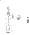
- FIG. 1 illustrates in block diagram form an acoustic imaging system 1.
- Acoustic imaging system 1 includes an acoustic probe 10 with a curved two dimensional acoustic array 12, connected via a cable 16 to a system beamformer 22, which is in turn connected to a controller 24 and a system image processor 24.
- Acoustic imaging system 1 also includes user controls 20 and a display 30.
- Acoustic probe 10 includes a two dimensional acoustic array 12, which in this example is curved in the elevation dimension. Under the ultimate control of controls 20, the acoustic elements of acoustic array 12 transmit acoustic one or more acoustic beams in the desired directions and to the desired focal points in the three dimensional image field in front of acoustic array 12. Echoes from the transmitted beams may be received by the acoustic transducer elements of acoustic array 12. Output signals of acoustic array 12 are provided via cable 16 to system beamformer 22, to ultimately generate an image which is displayed on display 30.
- FIG. 2 illustrates a portion of an acoustic array 12 which may be employed in acoustic imaging system 1.
- Acoustic array 12 comprises two or more acoustic array components, two of which are illustrated in FIG. 2 as first acoustic array component 11-1 and second acoustic array component 11-2. It should be understand that in general, acoustic array 12 may comprise any number of acoustic array components arranged in one or two dimensional arrays.
- First and second acoustic array components 11-1 and 11-2 each comprise an array of acoustic elements 2.
- Each acoustic element 2 includes an acoustic transducer element 3, and a corresponding acoustic element circuit 4 for coupling an electrical signal to acoustic transducer element 3 and receiving an electric signal from acoustic transducer element 3.
- Each acoustic element circuit 4 has a corresponding pad 5 formed within a circuitry area of the corresponding acoustic element circuit.
- Each acoustic element 2 further includes an interconnection bump 6 providing an electrical connection between the corresponding pad 5 and the corresponding acoustic transducer element 3.
- first and second acoustic array components 11-1 and 11-2 are provided on corresponding first and second semiconductor dies 7-1 and 7-2 where corresponding groups of the acoustic element circuits 4 are provided contiguous to each other.
- each of the semiconductor dies 7-1 and 7-2 include a border 8 along each edge thereof corresponding to a scribe lane on the original semiconductor wafer from which the dies were produced.
- First and second acoustic array components 11-1 and 11-2 may be provided on a surface of an acoustic probe, for example a curved surface.
- first and second acoustic array components 11-1 and 11-2 are separated and spaced apart from each other by a space 13.
- FIG. 3 illustrates an example embodiment of a circuit region 1000 of a substrate, where circuit region 1000 includes an array of acoustic element circuits 1002.
- acoustic element circuits 1002 are disposed contiguous to each other at a first pitch P1.
- pitch is understood to mean an average spacing between the centers of two elements which are closest to each other, allowing for the case of a uniform spacing as well as any other distribution with the same location of the end elements as a uniformly spaced distribution would have.
- the first pitch PI represents the average spacing between the centers of two elements which are closest to each other (i.e., adjacent).
- the first pitch PI may be uniform or substantially uniform among acoustic element circuits 1002 of circuit region 1000.
- FIG. 3 illustrates an embodiment where the array of acoustic element circuits 1002 is a two-dimensional array arranged in M rows each extending in the X direction and N columns each extending in the Y direction, where each row includes a first acoustic element circuit 1002-1 at a first end thereof, and a last acoustic element circuit 1002- N at a second (opposite) end thereof.
- acoustic element circuits 1002 are disposed contiguous to each other at the first pitch P1 in both the X direction and the Y direction.
- the array may be linear, or acoustic element circuits 1002 may have the first pitch P1 only in one direction.
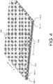
- FIG. 4 illustrates an example embodiment of a circuit region 1000 of a substrate, where circuit region 1000 includes an array of acoustic element circuits 1002 each having a corresponding pad 1004. Each pad 1004 is provided for electrical interconnection between the corresponding acoustic element circuit 1002 and a corresponding external component, for example an acoustic transducer element.
- FIG. 4 only shows pads 1004 for some of acoustic element circuits 1002, including the first row of the array of acoustic element circuits 1002, from a first pad 1004-1 for first acoustic element circuit 1002-1, to a last pad 1004- N for last acoustic element circuit 1002- N .
- each of the acoustic element circuits 1002 has its own corresponding pad 1004.
- pads 1004 form an array of pads 1004 disposed at a second pitch P2
- pitch is understood to mean an average spacing between the centers of two elements which are closest to each other, allowing for the case of a uniform spacing as well as any other distribution with the same location of the end elements as a uniformly spaced distribution would have.
- the second pitch P2 represents the average spacing between the centers of two elements which are closest to each other (i.e., adjacent).
- the second pitch P2 may be uniform or substantially uniform among pads 1004.
- pads 1004 are disposed at the second pitch P2 in both the X direction and the Y direction.
- the array may be linear, or pads 1004 may have the second pitch P2 only in one direction.
- first pad 1004-1 and last pad 1004- N are disposed along opposite sides of the corresponding acoustic element circuits 1002-1 and 1002- N with respect to each other.
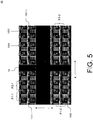
- FIG. 5 illustrates a portion of an example embodiment of a semiconductor wafer comprising a substrate 50 having a plurality of circuit regions 1000, including a first circuit region 1000-1 and a second circuit region 1000-2 which are separated and spaced apart from each other by a scribe lane 55.
- substrate 50 includes a plurality of circuit regions, including third and fourth circuit regions, wherein the first, second, third, and fourth circuit regions form a two dimensional array and are separated and spaced apart from each other by one or more scribing lanes 55.
- Each circuit region 1000 includes an array of acoustic element circuits 1002 having the first pitch P1-1 in the X direction.
- Each acoustic element circuit 1002 has a corresponding pad 1004 formed within a circuitry area of the corresponding acoustic element circuit 1002.
- pads 1004 are disposed at the second pitch P2-1 in the X direction, where the second pitch P2-1 is greater than the first pitch P1-1.
- first pad 1004-1 and last pad 1004- N in each row of each circuit region 1000 are disposed along opposite sides of the corresponding acoustic element circuits 1002-1 and 1002- N with respect to each other.
- pads 1004 of first and second circuit regions 1000-1 and 1000-2 together form an array of pads 1004, wherein pads 1004 of first and second circuit regions 1000-1 and 1000-2 may have a uniform or substantially uniform pitch throughout the array of pads 1004 in at least the X direction, where the uniform or substantially uniform pitch is the second pitch P2-1.
- FIG. 5 shows that acoustic element circuits 1002 and pads 1004 are each disposed in a two dimensional array of rows and columns, extending respectively in the X direction and Y direction. Accordingly, the array of acoustic element circuits 1002 has the pitch P1-1 in the X direction and a pitch P1-2 in the Y direction. In some embodiments, P1-1 is the same as P1-2. However, in some embodiments P1-1 may be different than P1-2. Similarly, the array of pads 1004 has the pitch P2-1 in the X direction and a pitch P2-2 in the Y direction. In some embodiments, P2-1 is the same as P2-2. However, in some embodiments P2-1 may be different than P2-2.
- FIG. 6 illustrates an example embodiment of a device 60 including an array of acoustic element circuits each having a corresponding pad 1004 and an interconnection bump 1005, and an acoustic transducer 2000 disposed on interconnection bumps 1005.
- first pad 1004-1 and last pad 1004- N are disposed along opposite sides of the corresponding acoustic element circuits 1002 with respect to each other.
- Each of the interconnection bumps 1005 is electrically conductive and in electrical contact or connection with a corresponding one of the pads 1004 and electrically connects the pad 1004, and thereby the corresponding acoustic element circuit, with acoustic transducer 2000.
- Acoustic transducer 2000 which for example may be a piezoelectric transducer, is configured to convert a received electrical signal to a sound wave, and conversely to convert a received sound wave to an electrical signal.
- Interconnection bumps 1005 are disposed at a third pitch P3 in at least the X direction (and in some embodiments, in both the X direction and the Y direction).
- pitch is understood to mean an average spacing between the centers of two elements which are closest to each other, allowing for the case of a uniform spacing as well as any other distribution with the same location of the end elements as a uniformly spaced distribution would have.
- the third pitch P3 represents the average spacing between the centers of two elements which are closest to each other (i.e., adjacent).
- the third pitch P3 may be uniform or substantially uniform among interconnection bumps 1005.
- the third pitch P3 of interconnection bumps 1005 may be different from the second pitch P2 of pads 1004 and/or the first pitch P1 of acoustic element circuits 1002.
- the third pitch P3 of interconnection bumps 1005 may be the same as or substantially the same as the second pitch P2 of pads 1004, while in other embodiments, the third pitch P3 of interconnection bumps 1005 may be the same as or substantially the same as the first pitch P1 of acoustic element circuits 1002.
- FIG. 7 illustrates a first example embodiment of a device 70 including an array of acoustic element circuits each having a corresponding pad 1004 and an interconnection bump 1005, and plurality of acoustic transducer elements 2002 disposed on the interconnection bumps 1005.
- FIG. 8 illustrates a first example embodiment of an acoustic array component 80 including an array of acoustic elements 3000.
- Each acoustic element 3000 includes an acoustic element circuit 1002, with a corresponding pad 1004, an acoustic transducer element 2002, and an interconnection bump 1005.
- acoustic array component 80 comprises: an array of acoustic element circuits 1002 disposed contiguous to each other at a first pitch P1; a plurality of pads 1004 each corresponding to one of the acoustic element circuits 1002 and formed within a circuitry area of the corresponding acoustic element circuit 1002, pads 1004 being disposed at a second pitch P2; a plurality of interconnection bumps 1005 each corresponding to one of the pads 1004 and being disposed in electrical connection with the corresponding pad 1004; and a plurality of acoustic transducer elements 2002 disposed on the interconnection bumps.
- the array of acoustic elements 3000 may be two dimensional, in which case the array of acoustic element circuits 1002, pads 1004, etc. may also be two dimensional.
- first pad 1004-1 and last pad 1004- N are disposed along opposite sides of the corresponding acoustic element circuits 1002 with respect to each other.
- Interconnection bumps 1005 are disposed at the third pitch P3 as discussed above with respect to FIG. 6 .
- acoustic transducer elements 2002 are disposed at a fourth pitch P4 in at least the X direction (and in some embodiments, in both the X direction and the Y direction, which is into the page in FIG. 8 ).
- pitch is understood to mean an average spacing between the centers of two elements which are closest to each other, allowing for the case of a uniform spacing as well as any other distribution with the same location of the end elements as a uniformly spaced distribution would have.
- the fourth pitch P4 represents the average spacing between the centers of two elements which are closest to each other (i.e., adjacent).
- the fourth pitch P4 may be uniform or substantially uniform throughout acoustic array component 80.
- the third pitch P3 of interconnection bumps 1005 is the same or substantially the same as the first pitch P1 of the acoustic element circuits 1002.
- the fourth pitch P4 of acoustic transducer elements 2002 is also the same or substantially the same as the first pitch P1 of the acoustic element circuits 1002.
- FIG. 9 illustrates a second example embodiment of an acoustic array component 90 including an array of acoustic elements 3000.
- Acoustic array component 90 is similar to acoustic array component 80, and so for brevity of explanation, only the differences will be discussed.
- the third pitch P3 of interconnection bumps 1005 is the same or substantially the same as the second pitch P2 of pads 1004.
- the fourth pitch P4 of acoustic transducer elements 2002 is the same or substantially the same as the first pitch P1 of the acoustic element circuits 1002.
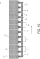
- FIG. 10 illustrates a third example embodiment of an acoustic array component 100 including an array of acoustic elements 3000.
- Acoustic array component 100 is similar to acoustic array component 80, and so for brevity of explanation, only the differences will be discussed.
- the third pitch P3 of interconnection bumps 1005 is the same or substantially the same as the second pitch P2 of pads 1004.
- the fourth pitch P4 of acoustic transducer elements 2002 is also the same or substantially the same as the second pitch P2 of pads 1004.
- FIG. 11 illustrates a portion of a first embodiment of an acoustic array 110 which may be employed in place of acoustic array 12 in imaging system 1 as illustrated in FIG. 1 .
- Acoustic array 110 includes a plurality of acoustic array components 100, including a first acoustic array component 100-1 and a second acoustic array component 100-2, which are spaced apart and separated by each other. Also shown in FIG. 11 are a ground plane 112 for the acoustic transducer elements 2002 of first and second acoustic array components 100-1 and 100-2, and a ground return 114 connected to ground plane 112.
- Acoustic array 110 may include a plurality of other acoustic array components 100 not shown in FIG. 11 .
- acoustic array may include a two dimensional array of acoustic array components 100, for example a 3 x 2 array.
- Acoustic circuit elements 1002 and pads 1004 of first acoustic array component 100-1 are formed in a first circuit region 1000-1, and the acoustic circuit elements 1002 and pads 1004 of second acoustic array component 100-2 are formed in a second circuit region 1000-2.
- Each of the first and second circuit regions 1000-1 and 1000-2 has a border 1008 along the edges or side thereof, which may comprise all or a portion of a scribe line for a die on which the corresponding circuit region 1000 is provided.
- the dies for first circuit region 1000-1 and second circuit region 1000-2 may be provided on a same semiconductor substrate as each other. In other embodiments, the dies for first circuit region 1000-1 and second circuit region 1000-2 may be provided on different semiconductor substrates from each other.
- first pad 1004-1 and last pad 1004- N are disposed along opposite sides of the corresponding acoustic element circuits 1002 with respect to each other.
- the third pitch P3 of interconnection bumps 1005 and the fourth pitch P4 of acoustic transducer elements 2002 are also the same or substantially the same as the second pitch P2 of pads 1004.
- the acoustic array components 100 of acoustic array 110 may be provided on a surface of an acoustic probe, for example a curved surface.
- the gap 1015 between the acoustic transducer element 2002 at one edge of first acoustic array component 100-1 and the adjacent acoustic transducer element 2002 at the adjacent and opposite edge of second acoustic array component 100-2 is the same or substantially the same as the gap between adjacent acoustic transducer element 2002 of the same acoustic array component 100.
- a uniform array of acoustic elements 3000 and in particular a uniform array of acoustic transducer elements 2002, can be provided even when acoustic elements 3000 are provided on two or more semiconductor dies (which may be on the same substrate, or on separate substrates).
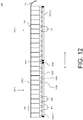
- FIG. 12 illustrates a portion of a second embodiment of an acoustic array 120 which may be employed in place of acoustic array 12 in imaging system 1 as illustrated in FIG. 1 .
- Acoustic array 120 is similar to acoustic array 110, and so for brevity of explanation, only the differences will be discussed.
- acoustic array 120 includes first and second acoustic array components 102-1 and 102-2 which may be identical or substantially identical to each other.
- Acoustic array 120 may include a plurality of other acoustic array components not shown in FIG. 12 .
- acoustic array may include a two dimensional array of acoustic array components 102, for example a 3 x 2 array.
- Acoustic array components 102-1 and 102-2 may each be similar to acoustic array component 100 illustrated in FIGs. 10 and 11 and discussed above, with a difference being that in acoustic array components 102-1 and 102-2, the third pitch P3 of interconnection bumps 1005 is greater than the second pitch P2 of pads 1004, while the fourth pitch P4 of acoustic transducer elements 2002 is the same or substantially the same as the second pitch P2 of pads 1004.
- the gap 1015 between the acoustic transducer element 2002 at one edge of first acoustic array component 102-1 and the adjacent acoustic transducer element 2002 at the adjacent and opposite edge of second acoustic array component 102-2 is the same or substantially the same as the gap between adjacent acoustic transducer element 2002 of the same acoustic array component 102.
- the construction of a uniform array of acoustic elements 3000, and in particular a uniform array of acoustic transducer elements 2002 can be provided even when acoustic elements 3000 are provided on two or more semiconductor dies (which may be on the same substrate, or on separate substrates).
- FIG. 13 illustrates a portion of a third embodiment of an acoustic array 130 which may be employed in place of acoustic array 12 in imaging system 1 as illustrated in FIG. 1 .
- Acoustic array 130 includes first and second acoustic array components 104-1 and 104-2 which may be identical or substantially identical to each other.
- Acoustic array 130 may include a plurality of other acoustic array components not shown in FIG. 13 .
- acoustic array may include a two dimensional array of acoustic array components 104, for example a 3 x 2 array.
- Acoustic circuit elements 1002 and pads 1004 of first acoustic array component 104-1 are formed in a first circuit region 1300-1, and the acoustic circuit elements 1002 and pads 1004 of second acoustic array component 104-2 are formed in a second circuit region 1300-2.
- Each of the first and second circuit regions 1000-1 and 1000-2 has border 1008 along the edges or side thereof, which may comprise all or a portion of a scribe line for a die on which the corresponding circuit region 1300 is provided.
- the dies for first circuit region 1300-1 and second circuit region 1300-2 may be provided on different semiconductor substrates from each other.
- first pad 1004-1 and last pad 1004- N are disposed in the same relative position in their corresponding acoustic element circuits 1002-1 and 1002- N as each other.
- the acoustic array components 104 of acoustic array 130 may be provided on a surface of an acoustic probe, for example a curved surface.
- the third pitch P3 of interconnection bumps 1005 is the same as the first pitch P1 of acoustic circuit elements 102 and the second pitch P2 of pads 1004, while the fourth pitch P4 of acoustic transducer elements 2002 is greater than the first pitch P1 of acoustic circuit elements 102, the second pitch P2 of pads 1004, and the third pitch P3 of interconnection bumps 1005.
- the gap 1015 between the acoustic transducer element 2002 at one edge of first acoustic array component 104-1 and the adjacent acoustic transducer element 2002 at the adjacent and opposite edge of second acoustic array component 104-2 is the same or substantially the same as the gap between adjacent acoustic transducer element 2002 of the same acoustic array component 104.
- the construction of a uniform array of acoustic elements 3000, and in particular a uniform array of acoustic transducer elements 2002, can be provided even when acoustic elements 3000 are provided on two or more different semiconductor dies.
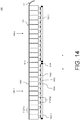
- FIG. 14 illustrates a portion of a fourth embodiment of an acoustic array 140 which may be employed in place of acoustic array 12 in imaging system 1 as illustrated in FIG. 1 .
- Acoustic array 140 is similar to acoustic array 110, and so for brevity of explanation, only the differences will be discussed.
- acoustic array 140 includes first and second acoustic array components 106-1 and 106-2 which may be identical or substantially identical to each other.
- Acoustic array 140 may include a plurality of other acoustic array components not shown in FIG. 14 .
- acoustic array may include a two dimensional array of acoustic array components 106, for example a 3 x 2 array.
- Acoustic array components 106-1 and 106-2 may each be similar to acoustic array component 104 illustrated in FIG. 13 and discussed above, with the difference being that in acoustic array components 106-1 and 106-2, the third pitch P3 of interconnection bumps 1005 is the same as the fourth pitch P4 of acoustic transducer elements 2002, so that both the third pitch P3 and the fourth pitch P4 are greater than the second pitch P2 of pads 1004 and the first pitch P1 of acoustic circuit elements 102.
- the gap 1015 between the acoustic transducer element 2002 at one edge of first acoustic array component 106-1 and the adjacent acoustic transducer element 2002 at the adjacent and opposite edge of second acoustic array component 106-2 is the same or substantially the same as the gap between adjacent acoustic transducer element 2002 of the same acoustic array component 106.
- the construction of a uniform array of acoustic elements 3000, and in particular a uniform array of acoustic transducer elements 2002 can be provided even when acoustic elements 3000 are provided on two or more different semiconductor dies.
- acoustic arrays 110, 120, 130 and 140 have been described in detail as example embodiments, in general it should be understood that other embodiments are possible, including, for example, acoustic arrays which employ acoustic array components 80 and 90 described above.
Landscapes
- Engineering & Computer Science (AREA)
- Physics & Mathematics (AREA)
- Radar, Positioning & Navigation (AREA)
- Remote Sensing (AREA)
- Mechanical Engineering (AREA)
- Computer Networks & Wireless Communication (AREA)
- General Physics & Mathematics (AREA)
- Acoustics & Sound (AREA)
- Transducers For Ultrasonic Waves (AREA)
- Ultra Sonic Daignosis Equipment (AREA)
- Investigating Or Analyzing Materials By The Use Of Ultrasonic Waves (AREA)
Claims (14)
- Vorrichtung, umfassend:eine akustische Sonde mit mehreren akustischen Anordnungskomponenten (11-1, 11-2, 100-1, 100-2), die voreinander getrennt und voneinander beabstandet sind, wobei jede der akustischen Anordnungskomponenten umfasst:eine Anordnung von akustischen Elementschaltungen (4, 1002), die in mindestens einer ersten Richtung in einem ersten Abstand nebeneinander angeordnet sind, wobei der Abstand ein durchschnittlicher Leerraum zwischen den Zentren zweier Elemente ist, die am nächsten zueinander angeordnet sind;eine Vielzahl von Pads (5, 1004), die jeweils einer der akustischen Elementschaltungen entsprechen, und in einem Schaltungsbereich der entsprechenden akustischen Elementschaltung ausgebildet sind, wobei die Pads in mindestens der ersten Richtung in einem zweiten Abstand angeordnet sind;eine Vielzahl von Verbindungshöckern (6, 1005), die jeweils einem der Pads entsprechen, und auf dem entsprechenden Pad angeordnet sind, und in elektrischem Kontakt mit diesem stehen, wobei die Verbindungshöcker in mindestens der ersten Richtung in einem dritten Abstand angeordnet sind; undeine Vielzahl von akustischen Wandlerelementen (3, 2002), die auf den Verbindungshöckern angeordnet sind, wobei die akustischen Wandlerelemente in mindestens der ersten Richtung in einem vierten Abstand angeordnet sind;wobei mindestens zwei der ersten, zweiten, dritten und vierten Abstände voneinander verschieden sind, undwobei jede der Verbindungshöcker elektrisch leitend ist, und die elektrische Verbindung zwischen dem entsprechenden Pad und dem entsprechenden akustischen Wandlerelement bereitstellt.
- Vorrichtung nach Anspruch 1, wobei der dritte Abstand größer als der zweite Abstand ist.
- Vorrichtung nach Anspruch 1, wobei der vierte Abstand größer als der dritte Abstand ist.
- Vorrichtung nach Anspruch 1, wobei der zweite Abstand größer als der erste Abstand ist.
- Vorrichtung nach Anspruch 4, wobei der zweite Abstand, der dritte Abstand und der vierte Abstand ungefähr gleich zueinander sind.
- Vorrichtung nach Anspruch 4, wobei der vierte Abstand im Wesentlichen derselbe als der zweite Abstand ist, und der dritte Abstand größer als der vierte Abstand ist.
- Vorrichtung nach Anspruch 1, wobei der zweite Abstand ungefähr gleich als der erste Abstand ist.
- Vorrichtung nach Anspruch 7, wobei entweder- der dritte Abstand ungefähr gleich als der erste Abstand ist, und der vierte Abstand größer als der erste Abstand ist, oder- der dritte Abstand größer als der erste Abstand ist, und der vierte Abstand ungefähr gleich als der dritte Abstand.
- Vorrichtung nach Anspruch 1, wobei mindestens eine erste akustische Anordnungskomponente und eine zweite akustische Anordnungskomponente unter der Vielzahl von akustischen Anordnungskomponenten zusammen auf einem gemeinsamen Halbleitersubstrat (50) vorgesehen sind, wobei die Pads der ersten und zweiten akustischen Anordnungskomponenten zusammen eine Pad-Anordnung bilden, und wobei die Pads der ersten und zweiten akustischen Anordnungskomponenten einen im Wesentlichen gleichmäßigen Abstand über die Pad-Anordnung aufweisen.
- Vorrichtung nach Anspruch 1, wobei mindestens eine erste akustische Anordnungskomponente und eine zweite akustische Anordnungskomponente unter der Vielzahl von akustischen Anordnungskomponenten auf voneinander verschiedenen Halbleitersubstraten vorgesehen sind, wobei die Pads der ersten und zweiten akustischen Anordnungskomponenten zusammen eine Pad-Anordnung bilden, und wobei die Pads der ersten und zweiten akustischen Anordnungskomponenten einen im Wesentlichen gleichmäßigen Abstand über die Pad-Anordnung aufweisen.
- Vorrichtung nach Anspruch 9 oder 10, wobei die akustischen Wandlerelemente der ersten und zweiten akustischen Anordnungskomponenten zusammen eine Anordnung von akustischen Wandlerelementen bilden, und wobei die akustischen Wandlerelemente der ersten und zweiten akustischen Anordnungskomponenten einen im Wesentlichen gleichmäßige Abstand über die Anordnung der akustischen Wandlerelemente aufweisen.
- Vorrichtung nach Anspruch 4, ferner umfassend:ein Substrat (50) mit mindestens einem ersten (1000-1) und einem zweiten (1000-2) Schaltungsbereich, wobei der erste Schaltungsbereich und der zweite Schaltungsbereich durch eine Anreißspur (55) zum Anreißen der Matrize von dem Substrat voreinander getrennt und voneinander beabstandet sind, wobei jeder der Schaltungsbereiche umfasst:die Anordnung von akustischen Elementschaltungen (1002), die in dem ersten Abstand (P1-1) in mindestens einer ersten Richtung angeordnet sind; unddie Vielzahl von Pads (1004), die jeweils einer der akustischen Elementschaltungen entsprechen, und in einem Schaltungsbereich der entsprechenden akustischen Elementschaltung ausgebildet sind;wobei die Pads des ersten und des zweiten Schaltungsbereichs zusammen eine Pad-Anordnung mit einer im Wesentlichen gleichmäßigen Abstand in mindestens der ersten Richtung über die Pad-Anordnung bilden.
- Vorrichtung nach Anspruch 12, wobei die Anordnung von akustischen Elementschaltungen umfasst:eine erste akustische Elementschaltung an einem ersten Ende der Anordnung, wobei das erste akustische Element ein entsprechendes erstes Pad aufweist; undeine letzte akustische Elementschaltung an einem zweiten Ende der Anordnung, das dem ersten Ende der Anordnung gegenüberliegt, wobei das letzte akustische Element ein entsprechendes letztes Pad aufweist;wobei die ersten und letzten Pads entlang gegenüberliegender Seiten der entsprechenden akustischen Elementschaltungen zueinander angeordnet sind.
- Vorrichtung nach Anspruch 12, wobei das Substrat mindestens einen dritten und einen vierten Schaltungsbereich umfasst, wobei der erste, zweite, dritte und vierte Schaltungsbereich eine zweidimensionale Anordnung bilden, und durch eine oder mehrere Anreißspuren voneinander getrennt und voneinander beabstandet sind.
Applications Claiming Priority (2)
| Application Number | Priority Date | Filing Date | Title |
|---|---|---|---|
| US201261746624P | 2012-12-28 | 2012-12-28 | |
| PCT/IB2013/061283 WO2014102712A2 (en) | 2012-12-28 | 2013-12-23 | Acoustic probe with components of acoustic elements having different pitches than each other |
Publications (2)
| Publication Number | Publication Date |
|---|---|
| EP2938440A2 EP2938440A2 (de) | 2015-11-04 |
| EP2938440B1 true EP2938440B1 (de) | 2020-12-02 |
Family
ID=50114424
Family Applications (1)
| Application Number | Title | Priority Date | Filing Date |
|---|---|---|---|
| EP13830113.0A Active EP2938440B1 (de) | 2012-12-28 | 2013-12-23 | Akustische sonde mit komponenten von akustikelementen mit unterschiedlichen abständen |
Country Status (5)
| Country | Link |
|---|---|
| US (1) | US9689973B2 (de) |
| EP (1) | EP2938440B1 (de) |
| JP (1) | JP6306048B2 (de) |
| CN (1) | CN104955586B (de) |
| WO (1) | WO2014102712A2 (de) |
Families Citing this family (2)
| Publication number | Priority date | Publication date | Assignee | Title |
|---|---|---|---|---|
| CN104955586B (zh) * | 2012-12-28 | 2018-05-15 | 皇家飞利浦有限公司 | 具有彼此不同间距的声学元件的部件的声学探头 |
| US10697939B2 (en) * | 2018-03-02 | 2020-06-30 | B-K Medical Aps | Synthetic fine-pitch ultrasound imaging |
Family Cites Families (14)
| Publication number | Priority date | Publication date | Assignee | Title |
|---|---|---|---|---|
| CN1234469C (zh) * | 2000-05-22 | 2006-01-04 | 有限会社三轮科学研究所 | 超声波辐射装置 |
| US6352510B1 (en) * | 2000-06-22 | 2002-03-05 | Leonid S. Barabash | Ultrasound transducers for real time two and three dimensional image acquisition |
| WO2006075283A2 (en) | 2005-01-11 | 2006-07-20 | Koninklijke Philips Electronics, N.V. | Redistribution interconnect for microbeamformer(s) and a medical ultrasound system |
| EP2046507B1 (de) * | 2006-07-24 | 2015-03-11 | Koninklijke Philips N.V. | Ultraschallwandler mit pitch-unabhängigem interposer und methode zu dessen herstellung |
| US7892176B2 (en) | 2007-05-02 | 2011-02-22 | General Electric Company | Monitoring or imaging system with interconnect structure for large area sensor array |
| JP5002402B2 (ja) | 2007-10-03 | 2012-08-15 | 株式会社東芝 | 超音波探触子及び超音波診断装置 |
| JP2010082501A (ja) * | 2008-09-29 | 2010-04-15 | Sanyo Electric Co Ltd | リニアモータおよびリニアモータを備える携帯機器 |
| US20100154190A1 (en) * | 2008-12-19 | 2010-06-24 | Sanger Kurt M | Method of making a composite device |
| CN101771917B (zh) * | 2008-12-30 | 2013-11-06 | 北京富纳特创新科技有限公司 | 发声装置 |
| US8207652B2 (en) * | 2009-06-16 | 2012-06-26 | General Electric Company | Ultrasound transducer with improved acoustic performance |
| JP2011011011A (ja) * | 2009-06-30 | 2011-01-20 | Kenji Shirato | 運動器具 |
| US8345508B2 (en) | 2009-09-20 | 2013-01-01 | General Electric Company | Large area modular sensor array assembly and method for making the same |
| JP5454890B2 (ja) * | 2009-11-24 | 2014-03-26 | 株式会社東芝 | 超音波プローブ及び超音波プローブの製造方法 |
| CN104955586B (zh) * | 2012-12-28 | 2018-05-15 | 皇家飞利浦有限公司 | 具有彼此不同间距的声学元件的部件的声学探头 |
-
2013
- 2013-12-23 CN CN201380068588.8A patent/CN104955586B/zh active Active
- 2013-12-23 WO PCT/IB2013/061283 patent/WO2014102712A2/en not_active Ceased
- 2013-12-23 US US14/654,877 patent/US9689973B2/en active Active
- 2013-12-23 EP EP13830113.0A patent/EP2938440B1/de active Active
- 2013-12-23 JP JP2015550187A patent/JP6306048B2/ja active Active
Non-Patent Citations (1)
| Title |
|---|
| None * |
Also Published As
| Publication number | Publication date |
|---|---|
| CN104955586A (zh) | 2015-09-30 |
| WO2014102712A3 (en) | 2014-11-13 |
| CN104955586B (zh) | 2018-05-15 |
| JP6306048B2 (ja) | 2018-04-04 |
| WO2014102712A2 (en) | 2014-07-03 |
| JP2016503990A (ja) | 2016-02-08 |
| US9689973B2 (en) | 2017-06-27 |
| EP2938440A2 (de) | 2015-11-04 |
| US20150338511A1 (en) | 2015-11-26 |
Similar Documents
| Publication | Publication Date | Title |
|---|---|---|
| US7892176B2 (en) | Monitoring or imaging system with interconnect structure for large area sensor array | |
| CN106469859B (zh) | 阵列天线的瓦片式系统和方法 | |
| KR20110031406A (ko) | 넓은 면적의 모듈러 센서 어레이 어셈블리, 변환기 센서 어레이 어셈블리, 넓은 면적의 모듈러 센서 어레이 어셈블리를 구성하는 방법 | |
| US7687976B2 (en) | Ultrasound imaging system | |
| JP5735512B2 (ja) | 大きな視野を持つ超音波プローブ及びこのような超音波プローブを製造する方法 | |
| US7795784B2 (en) | Redistribution interconnect for microbeamforming(s) and a medical ultrasound system | |
| JP2009044718A (ja) | 貫通ビア相互接続構造を有する超音波システム | |
| WO2008157260A3 (en) | System and method of acoustic doppler beamforming | |
| US10238365B2 (en) | Ultrasound probe | |
| US20110021921A1 (en) | Ultrasound diagnostic apparatus | |
| EP2938440B1 (de) | Akustische sonde mit komponenten von akustikelementen mit unterschiedlichen abständen | |
| CN101229070A (zh) | 2维阵列超声波探头以及超声波诊断系统 | |
| KR101148542B1 (ko) | 플립 칩 구성을 갖는 전기 소자 | |
| US9532767B2 (en) | Ultrasonic probe apparatus and method of manufacturing ultrasonic probe apparatus | |
| JP5454890B2 (ja) | 超音波プローブ及び超音波プローブの製造方法 | |
| JP2004040250A (ja) | 超音波振動子及びその製造方法 | |
| JP5345481B2 (ja) | 超音波診断装置 | |
| WO2018230261A1 (ja) | コンベックス型超音波プローブ | |
| JP7767477B2 (ja) | 多用途超音波マトリクスアレイシグナルプロセッサ | |
| JP2011050491A (ja) | 超音波診断装置 | |
| CN118371417A (zh) | 用于具有减小占地面积的模块化换能器探头的方法和系统 | |
| CN118179887A (zh) | 一种高密度二维相控阵列式压电微机械超声换能器 | |
| JP5409207B2 (ja) | 超音波診断装置 | |
| JP2005065884A (ja) | 超音波探触子及び超音波診断装置 |
Legal Events
| Date | Code | Title | Description |
|---|---|---|---|
| PUAI | Public reference made under article 153(3) epc to a published international application that has entered the european phase |
Free format text: ORIGINAL CODE: 0009012 |
|
| 17P | Request for examination filed |
Effective date: 20150728 |
|
| AK | Designated contracting states |
Kind code of ref document: A2 Designated state(s): AL AT BE BG CH CY CZ DE DK EE ES FI FR GB GR HR HU IE IS IT LI LT LU LV MC MK MT NL NO PL PT RO RS SE SI SK SM TR |
|
| AX | Request for extension of the european patent |
Extension state: BA ME |
|
| DAX | Request for extension of the european patent (deleted) | ||
| STAA | Information on the status of an ep patent application or granted ep patent |
Free format text: STATUS: EXAMINATION IS IN PROGRESS |
|
| 17Q | First examination report despatched |
Effective date: 20191024 |
|
| RAP1 | Party data changed (applicant data changed or rights of an application transferred) |
Owner name: KONINKLIJKE PHILIPS N.V. |
|
| GRAP | Despatch of communication of intention to grant a patent |
Free format text: ORIGINAL CODE: EPIDOSNIGR1 |
|
| STAA | Information on the status of an ep patent application or granted ep patent |
Free format text: STATUS: GRANT OF PATENT IS INTENDED |
|
| INTG | Intention to grant announced |
Effective date: 20200617 |
|
| GRAS | Grant fee paid |
Free format text: ORIGINAL CODE: EPIDOSNIGR3 |
|
| GRAA | (expected) grant |
Free format text: ORIGINAL CODE: 0009210 |
|
| STAA | Information on the status of an ep patent application or granted ep patent |
Free format text: STATUS: THE PATENT HAS BEEN GRANTED |
|
| AK | Designated contracting states |
Kind code of ref document: B1 Designated state(s): AL AT BE BG CH CY CZ DE DK EE ES FI FR GB GR HR HU IE IS IT LI LT LU LV MC MK MT NL NO PL PT RO RS SE SI SK SM TR |
|
| REG | Reference to a national code |
Ref country code: GB Ref legal event code: FG4D |
|
| REG | Reference to a national code |
Ref country code: AT Ref legal event code: REF Ref document number: 1340326 Country of ref document: AT Kind code of ref document: T Effective date: 20201215 Ref country code: CH Ref legal event code: EP |
|
| REG | Reference to a national code |
Ref country code: DE Ref legal event code: R096 Ref document number: 602013074497 Country of ref document: DE |
|
| REG | Reference to a national code |
Ref country code: IE Ref legal event code: FG4D |
|
| REG | Reference to a national code |
Ref country code: DE Ref legal event code: R084 Ref document number: 602013074497 Country of ref document: DE |
|
| REG | Reference to a national code |
Ref country code: GB Ref legal event code: 746 Effective date: 20210102 |
|
| PG25 | Lapsed in a contracting state [announced via postgrant information from national office to epo] |
Ref country code: FI Free format text: LAPSE BECAUSE OF FAILURE TO SUBMIT A TRANSLATION OF THE DESCRIPTION OR TO PAY THE FEE WITHIN THE PRESCRIBED TIME-LIMIT Effective date: 20201202 Ref country code: RS Free format text: LAPSE BECAUSE OF FAILURE TO SUBMIT A TRANSLATION OF THE DESCRIPTION OR TO PAY THE FEE WITHIN THE PRESCRIBED TIME-LIMIT Effective date: 20201202 Ref country code: NO Free format text: LAPSE BECAUSE OF FAILURE TO SUBMIT A TRANSLATION OF THE DESCRIPTION OR TO PAY THE FEE WITHIN THE PRESCRIBED TIME-LIMIT Effective date: 20210302 Ref country code: GR Free format text: LAPSE BECAUSE OF FAILURE TO SUBMIT A TRANSLATION OF THE DESCRIPTION OR TO PAY THE FEE WITHIN THE PRESCRIBED TIME-LIMIT Effective date: 20210303 |
|
| REG | Reference to a national code |
Ref country code: NL Ref legal event code: MP Effective date: 20201202 |
|
| REG | Reference to a national code |
Ref country code: AT Ref legal event code: MK05 Ref document number: 1340326 Country of ref document: AT Kind code of ref document: T Effective date: 20201202 |
|
| PG25 | Lapsed in a contracting state [announced via postgrant information from national office to epo] |
Ref country code: BG Free format text: LAPSE BECAUSE OF FAILURE TO SUBMIT A TRANSLATION OF THE DESCRIPTION OR TO PAY THE FEE WITHIN THE PRESCRIBED TIME-LIMIT Effective date: 20210302 Ref country code: LV Free format text: LAPSE BECAUSE OF FAILURE TO SUBMIT A TRANSLATION OF THE DESCRIPTION OR TO PAY THE FEE WITHIN THE PRESCRIBED TIME-LIMIT Effective date: 20201202 Ref country code: SE Free format text: LAPSE BECAUSE OF FAILURE TO SUBMIT A TRANSLATION OF THE DESCRIPTION OR TO PAY THE FEE WITHIN THE PRESCRIBED TIME-LIMIT Effective date: 20201202 Ref country code: PL Free format text: LAPSE BECAUSE OF FAILURE TO SUBMIT A TRANSLATION OF THE DESCRIPTION OR TO PAY THE FEE WITHIN THE PRESCRIBED TIME-LIMIT Effective date: 20201202 |
|
| PG25 | Lapsed in a contracting state [announced via postgrant information from national office to epo] |
Ref country code: NL Free format text: LAPSE BECAUSE OF FAILURE TO SUBMIT A TRANSLATION OF THE DESCRIPTION OR TO PAY THE FEE WITHIN THE PRESCRIBED TIME-LIMIT Effective date: 20201202 Ref country code: HR Free format text: LAPSE BECAUSE OF FAILURE TO SUBMIT A TRANSLATION OF THE DESCRIPTION OR TO PAY THE FEE WITHIN THE PRESCRIBED TIME-LIMIT Effective date: 20201202 |
|
| REG | Reference to a national code |
Ref country code: LT Ref legal event code: MG9D |
|
| PG25 | Lapsed in a contracting state [announced via postgrant information from national office to epo] |
Ref country code: PT Free format text: LAPSE BECAUSE OF FAILURE TO SUBMIT A TRANSLATION OF THE DESCRIPTION OR TO PAY THE FEE WITHIN THE PRESCRIBED TIME-LIMIT Effective date: 20210405 Ref country code: RO Free format text: LAPSE BECAUSE OF FAILURE TO SUBMIT A TRANSLATION OF THE DESCRIPTION OR TO PAY THE FEE WITHIN THE PRESCRIBED TIME-LIMIT Effective date: 20201202 Ref country code: SK Free format text: LAPSE BECAUSE OF FAILURE TO SUBMIT A TRANSLATION OF THE DESCRIPTION OR TO PAY THE FEE WITHIN THE PRESCRIBED TIME-LIMIT Effective date: 20201202 Ref country code: LT Free format text: LAPSE BECAUSE OF FAILURE TO SUBMIT A TRANSLATION OF THE DESCRIPTION OR TO PAY THE FEE WITHIN THE PRESCRIBED TIME-LIMIT Effective date: 20201202 Ref country code: SM Free format text: LAPSE BECAUSE OF FAILURE TO SUBMIT A TRANSLATION OF THE DESCRIPTION OR TO PAY THE FEE WITHIN THE PRESCRIBED TIME-LIMIT Effective date: 20201202 Ref country code: EE Free format text: LAPSE BECAUSE OF FAILURE TO SUBMIT A TRANSLATION OF THE DESCRIPTION OR TO PAY THE FEE WITHIN THE PRESCRIBED TIME-LIMIT Effective date: 20201202 Ref country code: CZ Free format text: LAPSE BECAUSE OF FAILURE TO SUBMIT A TRANSLATION OF THE DESCRIPTION OR TO PAY THE FEE WITHIN THE PRESCRIBED TIME-LIMIT Effective date: 20201202 |
|
| REG | Reference to a national code |
Ref country code: CH Ref legal event code: PL |
|
| PG25 | Lapsed in a contracting state [announced via postgrant information from national office to epo] |
Ref country code: AT Free format text: LAPSE BECAUSE OF FAILURE TO SUBMIT A TRANSLATION OF THE DESCRIPTION OR TO PAY THE FEE WITHIN THE PRESCRIBED TIME-LIMIT Effective date: 20201202 |
|
| REG | Reference to a national code |
Ref country code: DE Ref legal event code: R097 Ref document number: 602013074497 Country of ref document: DE Ref country code: BE Ref legal event code: MM Effective date: 20201231 |
|
| PG25 | Lapsed in a contracting state [announced via postgrant information from national office to epo] |
Ref country code: MC Free format text: LAPSE BECAUSE OF FAILURE TO SUBMIT A TRANSLATION OF THE DESCRIPTION OR TO PAY THE FEE WITHIN THE PRESCRIBED TIME-LIMIT Effective date: 20201202 Ref country code: IS Free format text: LAPSE BECAUSE OF FAILURE TO SUBMIT A TRANSLATION OF THE DESCRIPTION OR TO PAY THE FEE WITHIN THE PRESCRIBED TIME-LIMIT Effective date: 20210402 |
|
| PLBE | No opposition filed within time limit |
Free format text: ORIGINAL CODE: 0009261 |
|
| STAA | Information on the status of an ep patent application or granted ep patent |
Free format text: STATUS: NO OPPOSITION FILED WITHIN TIME LIMIT |
|
| PG25 | Lapsed in a contracting state [announced via postgrant information from national office to epo] |
Ref country code: IT Free format text: LAPSE BECAUSE OF FAILURE TO SUBMIT A TRANSLATION OF THE DESCRIPTION OR TO PAY THE FEE WITHIN THE PRESCRIBED TIME-LIMIT Effective date: 20201202 Ref country code: IE Free format text: LAPSE BECAUSE OF NON-PAYMENT OF DUE FEES Effective date: 20201223 Ref country code: AL Free format text: LAPSE BECAUSE OF FAILURE TO SUBMIT A TRANSLATION OF THE DESCRIPTION OR TO PAY THE FEE WITHIN THE PRESCRIBED TIME-LIMIT Effective date: 20201202 Ref country code: LU Free format text: LAPSE BECAUSE OF NON-PAYMENT OF DUE FEES Effective date: 20201223 |
|
| 26N | No opposition filed |
Effective date: 20210903 |
|
| PG25 | Lapsed in a contracting state [announced via postgrant information from national office to epo] |
Ref country code: LI Free format text: LAPSE BECAUSE OF NON-PAYMENT OF DUE FEES Effective date: 20201231 Ref country code: SI Free format text: LAPSE BECAUSE OF FAILURE TO SUBMIT A TRANSLATION OF THE DESCRIPTION OR TO PAY THE FEE WITHIN THE PRESCRIBED TIME-LIMIT Effective date: 20201202 Ref country code: ES Free format text: LAPSE BECAUSE OF FAILURE TO SUBMIT A TRANSLATION OF THE DESCRIPTION OR TO PAY THE FEE WITHIN THE PRESCRIBED TIME-LIMIT Effective date: 20201202 Ref country code: DK Free format text: LAPSE BECAUSE OF FAILURE TO SUBMIT A TRANSLATION OF THE DESCRIPTION OR TO PAY THE FEE WITHIN THE PRESCRIBED TIME-LIMIT Effective date: 20201202 Ref country code: CH Free format text: LAPSE BECAUSE OF NON-PAYMENT OF DUE FEES Effective date: 20201231 |
|
| PG25 | Lapsed in a contracting state [announced via postgrant information from national office to epo] |
Ref country code: IS Free format text: LAPSE BECAUSE OF FAILURE TO SUBMIT A TRANSLATION OF THE DESCRIPTION OR TO PAY THE FEE WITHIN THE PRESCRIBED TIME-LIMIT Effective date: 20210402 Ref country code: TR Free format text: LAPSE BECAUSE OF FAILURE TO SUBMIT A TRANSLATION OF THE DESCRIPTION OR TO PAY THE FEE WITHIN THE PRESCRIBED TIME-LIMIT Effective date: 20201202 Ref country code: MT Free format text: LAPSE BECAUSE OF FAILURE TO SUBMIT A TRANSLATION OF THE DESCRIPTION OR TO PAY THE FEE WITHIN THE PRESCRIBED TIME-LIMIT Effective date: 20201202 Ref country code: CY Free format text: LAPSE BECAUSE OF FAILURE TO SUBMIT A TRANSLATION OF THE DESCRIPTION OR TO PAY THE FEE WITHIN THE PRESCRIBED TIME-LIMIT Effective date: 20201202 |
|
| PG25 | Lapsed in a contracting state [announced via postgrant information from national office to epo] |
Ref country code: MK Free format text: LAPSE BECAUSE OF FAILURE TO SUBMIT A TRANSLATION OF THE DESCRIPTION OR TO PAY THE FEE WITHIN THE PRESCRIBED TIME-LIMIT Effective date: 20201202 |
|
| PG25 | Lapsed in a contracting state [announced via postgrant information from national office to epo] |
Ref country code: BE Free format text: LAPSE BECAUSE OF NON-PAYMENT OF DUE FEES Effective date: 20201231 |
|
| PGFP | Annual fee paid to national office [announced via postgrant information from national office to epo] |
Ref country code: FR Payment date: 20231226 Year of fee payment: 11 |
|
| PGFP | Annual fee paid to national office [announced via postgrant information from national office to epo] |
Ref country code: GB Payment date: 20241217 Year of fee payment: 12 |
|
| PGFP | Annual fee paid to national office [announced via postgrant information from national office to epo] |
Ref country code: DE Payment date: 20241227 Year of fee payment: 12 |
|
| PG25 | Lapsed in a contracting state [announced via postgrant information from national office to epo] |
Ref country code: FR Free format text: LAPSE BECAUSE OF NON-PAYMENT OF DUE FEES Effective date: 20241231 |