EP2933827A1 - Transistor having nitride semiconductor used therein and method for manufacturing transistor having nitride semiconductor used therein - Google Patents
Transistor having nitride semiconductor used therein and method for manufacturing transistor having nitride semiconductor used therein Download PDFInfo
- Publication number
- EP2933827A1 EP2933827A1 EP12890237.6A EP12890237A EP2933827A1 EP 2933827 A1 EP2933827 A1 EP 2933827A1 EP 12890237 A EP12890237 A EP 12890237A EP 2933827 A1 EP2933827 A1 EP 2933827A1
- Authority
- EP
- European Patent Office
- Prior art keywords
- layer
- gate electrode
- insulating film
- transistor
- spacer layer
- Prior art date
- Legal status (The legal status is an assumption and is not a legal conclusion. Google has not performed a legal analysis and makes no representation as to the accuracy of the status listed.)
- Granted
Links
Images



Classifications
-
- H—ELECTRICITY
- H10—SEMICONDUCTOR DEVICES; ELECTRIC SOLID-STATE DEVICES NOT OTHERWISE PROVIDED FOR
- H10D—INORGANIC ELECTRIC SEMICONDUCTOR DEVICES
- H10D30/00—Field-effect transistors [FET]
- H10D30/40—FETs having zero-dimensional [0D], one-dimensional [1D] or two-dimensional [2D] charge carrier gas channels
- H10D30/47—FETs having zero-dimensional [0D], one-dimensional [1D] or two-dimensional [2D] charge carrier gas channels having two-dimensional [2D] charge carrier gas channels, e.g. nanoribbon FETs or high electron mobility transistors [HEMT]
- H10D30/471—High electron mobility transistors [HEMT] or high hole mobility transistors [HHMT]
- H10D30/475—High electron mobility transistors [HEMT] or high hole mobility transistors [HHMT] having wider bandgap layer formed on top of lower bandgap active layer, e.g. undoped barrier HEMTs such as i-AlGaN/GaN HEMTs
- H10D30/4755—High electron mobility transistors [HEMT] or high hole mobility transistors [HHMT] having wider bandgap layer formed on top of lower bandgap active layer, e.g. undoped barrier HEMTs such as i-AlGaN/GaN HEMTs having wide bandgap charge-carrier supplying layers, e.g. modulation doped HEMTs such as n-AlGaAs/GaAs HEMTs
-
- H—ELECTRICITY
- H10—SEMICONDUCTOR DEVICES; ELECTRIC SOLID-STATE DEVICES NOT OTHERWISE PROVIDED FOR
- H10D—INORGANIC ELECTRIC SEMICONDUCTOR DEVICES
- H10D30/00—Field-effect transistors [FET]
- H10D30/01—Manufacture or treatment
- H10D30/015—Manufacture or treatment of FETs having heterojunction interface channels or heterojunction gate electrodes, e.g. HEMT
-
- H—ELECTRICITY
- H10—SEMICONDUCTOR DEVICES; ELECTRIC SOLID-STATE DEVICES NOT OTHERWISE PROVIDED FOR
- H10D—INORGANIC ELECTRIC SEMICONDUCTOR DEVICES
- H10D30/00—Field-effect transistors [FET]
- H10D30/40—FETs having zero-dimensional [0D], one-dimensional [1D] or two-dimensional [2D] charge carrier gas channels
- H10D30/47—FETs having zero-dimensional [0D], one-dimensional [1D] or two-dimensional [2D] charge carrier gas channels having two-dimensional [2D] charge carrier gas channels, e.g. nanoribbon FETs or high electron mobility transistors [HEMT]
- H10D30/471—High electron mobility transistors [HEMT] or high hole mobility transistors [HHMT]
- H10D30/475—High electron mobility transistors [HEMT] or high hole mobility transistors [HHMT] having wider bandgap layer formed on top of lower bandgap active layer, e.g. undoped barrier HEMTs such as i-AlGaN/GaN HEMTs
-
- H—ELECTRICITY
- H10—SEMICONDUCTOR DEVICES; ELECTRIC SOLID-STATE DEVICES NOT OTHERWISE PROVIDED FOR
- H10D—INORGANIC ELECTRIC SEMICONDUCTOR DEVICES
- H10D62/00—Semiconductor bodies, or regions thereof, of devices having potential barriers
- H10D62/10—Shapes, relative sizes or dispositions of the regions of the semiconductor bodies; Shapes of the semiconductor bodies
- H10D62/17—Semiconductor regions connected to electrodes not carrying current to be rectified, amplified or switched, e.g. channel regions
- H10D62/213—Channel regions of field-effect devices
- H10D62/221—Channel regions of field-effect devices of FETs
-
- H—ELECTRICITY
- H10—SEMICONDUCTOR DEVICES; ELECTRIC SOLID-STATE DEVICES NOT OTHERWISE PROVIDED FOR
- H10D—INORGANIC ELECTRIC SEMICONDUCTOR DEVICES
- H10D62/00—Semiconductor bodies, or regions thereof, of devices having potential barriers
- H10D62/80—Semiconductor bodies, or regions thereof, of devices having potential barriers characterised by the materials
- H10D62/82—Heterojunctions
- H10D62/824—Heterojunctions comprising only Group III-V materials heterojunctions, e.g. GaN/AlGaN heterojunctions
-
- H—ELECTRICITY
- H10—SEMICONDUCTOR DEVICES; ELECTRIC SOLID-STATE DEVICES NOT OTHERWISE PROVIDED FOR
- H10D—INORGANIC ELECTRIC SEMICONDUCTOR DEVICES
- H10D62/00—Semiconductor bodies, or regions thereof, of devices having potential barriers
- H10D62/80—Semiconductor bodies, or regions thereof, of devices having potential barriers characterised by the materials
- H10D62/85—Semiconductor bodies, or regions thereof, of devices having potential barriers characterised by the materials being Group III-V materials, e.g. GaAs
- H10D62/852—Semiconductor bodies, or regions thereof, of devices having potential barriers characterised by the materials being Group III-V materials, e.g. GaAs being Group III-V materials comprising three or more elements, e.g. AlGaN or InAsSbP
-
- H—ELECTRICITY
- H10—SEMICONDUCTOR DEVICES; ELECTRIC SOLID-STATE DEVICES NOT OTHERWISE PROVIDED FOR
- H10D—INORGANIC ELECTRIC SEMICONDUCTOR DEVICES
- H10D64/00—Electrodes of devices having potential barriers
- H10D64/20—Electrodes characterised by their shapes, relative sizes or dispositions
- H10D64/27—Electrodes not carrying the current to be rectified, amplified, oscillated or switched, e.g. gates
- H10D64/311—Gate electrodes for field-effect devices
- H10D64/411—Gate electrodes for field-effect devices for FETs
- H10D64/511—Gate electrodes for field-effect devices for FETs for IGFETs
- H10D64/517—Gate electrodes for field-effect devices for FETs for IGFETs characterised by the conducting layers
- H10D64/518—Gate electrodes for field-effect devices for FETs for IGFETs characterised by the conducting layers characterised by their lengths or sectional shapes
-
- H—ELECTRICITY
- H10—SEMICONDUCTOR DEVICES; ELECTRIC SOLID-STATE DEVICES NOT OTHERWISE PROVIDED FOR
- H10D—INORGANIC ELECTRIC SEMICONDUCTOR DEVICES
- H10D30/00—Field-effect transistors [FET]
- H10D30/40—FETs having zero-dimensional [0D], one-dimensional [1D] or two-dimensional [2D] charge carrier gas channels
- H10D30/47—FETs having zero-dimensional [0D], one-dimensional [1D] or two-dimensional [2D] charge carrier gas channels having two-dimensional [2D] charge carrier gas channels, e.g. nanoribbon FETs or high electron mobility transistors [HEMT]
-
- H—ELECTRICITY
- H10—SEMICONDUCTOR DEVICES; ELECTRIC SOLID-STATE DEVICES NOT OTHERWISE PROVIDED FOR
- H10D—INORGANIC ELECTRIC SEMICONDUCTOR DEVICES
- H10D30/00—Field-effect transistors [FET]
- H10D30/40—FETs having zero-dimensional [0D], one-dimensional [1D] or two-dimensional [2D] charge carrier gas channels
- H10D30/47—FETs having zero-dimensional [0D], one-dimensional [1D] or two-dimensional [2D] charge carrier gas channels having two-dimensional [2D] charge carrier gas channels, e.g. nanoribbon FETs or high electron mobility transistors [HEMT]
- H10D30/471—High electron mobility transistors [HEMT] or high hole mobility transistors [HHMT]
- H10D30/473—High electron mobility transistors [HEMT] or high hole mobility transistors [HHMT] having confinement of carriers by multiple heterojunctions, e.g. quantum well HEMT
-
- H—ELECTRICITY
- H10—SEMICONDUCTOR DEVICES; ELECTRIC SOLID-STATE DEVICES NOT OTHERWISE PROVIDED FOR
- H10D—INORGANIC ELECTRIC SEMICONDUCTOR DEVICES
- H10D30/00—Field-effect transistors [FET]
- H10D30/40—FETs having zero-dimensional [0D], one-dimensional [1D] or two-dimensional [2D] charge carrier gas channels
- H10D30/47—FETs having zero-dimensional [0D], one-dimensional [1D] or two-dimensional [2D] charge carrier gas channels having two-dimensional [2D] charge carrier gas channels, e.g. nanoribbon FETs or high electron mobility transistors [HEMT]
- H10D30/471—High electron mobility transistors [HEMT] or high hole mobility transistors [HHMT]
- H10D30/477—Vertical HEMTs or vertical HHMTs
-
- H—ELECTRICITY
- H10—SEMICONDUCTOR DEVICES; ELECTRIC SOLID-STATE DEVICES NOT OTHERWISE PROVIDED FOR
- H10D—INORGANIC ELECTRIC SEMICONDUCTOR DEVICES
- H10D62/00—Semiconductor bodies, or regions thereof, of devices having potential barriers
- H10D62/80—Semiconductor bodies, or regions thereof, of devices having potential barriers characterised by the materials
- H10D62/85—Semiconductor bodies, or regions thereof, of devices having potential barriers characterised by the materials being Group III-V materials, e.g. GaAs
- H10D62/8503—Nitride Group III-V materials, e.g. AlN or GaN
-
- H—ELECTRICITY
- H10—SEMICONDUCTOR DEVICES; ELECTRIC SOLID-STATE DEVICES NOT OTHERWISE PROVIDED FOR
- H10D—INORGANIC ELECTRIC SEMICONDUCTOR DEVICES
- H10D64/00—Electrodes of devices having potential barriers
- H10D64/20—Electrodes characterised by their shapes, relative sizes or dispositions
- H10D64/27—Electrodes not carrying the current to be rectified, amplified, oscillated or switched, e.g. gates
- H10D64/311—Gate electrodes for field-effect devices
- H10D64/411—Gate electrodes for field-effect devices for FETs
Definitions
- the present invention relates to a high electron mobility transistor (HEMT) having a nitride semiconductor represented by GaN (gallium nitride), and a method for manufacturing this transistor.
- HEMT high electron mobility transistor
- GaN gallium nitride
- Non-Patent Document 1 a sectional view of the structure of the GaN HEMT having the AlN spacer is published.
- AlN spacer layer AlN
- AlGaN barrier layer
- Si3N4 a nitride film
- the GaN HEMT is used in a high-output and high-frequency amplifier or a power switch circuit.
- Fig. 1 is a schematic sectional view showing an example of a structure of a conventional high electron mobility transistor having a nitride semiconductor used therein (GaN HEMT).
- this conventional GaN HEMT is configured by inserting an AlN spacer, and includes a substrate 1, a buffer layer 2, a channel layer 3, a spacer layer 4, a barrier layer 5, an insulating film layer 6, a source electrode 7, a drain electrode 8, and a gate electrode 9.
- the AlN spacer layer 4 is present on the whole surface including the vicinity directly below the gate electrode 9.
- Non-Patent Document 1 Balaji Padmanabhan, Dragicarissaska and Stephen. M Goodnick, "Modeling Reliability of GaN/AlGaN/AlN/GaN HEMT", ISDRS 2011, December 7-9, 2011
- the present invention has been made in order to solve the above problem, and an object of the invention is to provide a transistor having a nitride semiconductor used therein that has high reliability while suppressing increase in access resistance, and a method for manufacturing a transistor having a nitride semiconductor used therein.
- a transistor having a nitride semiconductor used therein includes: a channel layer through which electrons run; a barrier layer that forms a two-dimensional electron gas in the channel layer and that is provided above the channel layer and contains at least one of indium, aluminum and gallium, and nitrogen; and a gate electrode, a source electrode, and a drain electrode that are arranged on the barrier layer, and further includes a spacer layer that is inserted between the barrier layer and the channel layer, and that is larger in polarization than the barrier layer, wherein the spacer layer is not present only in a region directly below the gate electrode and in a vicinity of the region.
- the AlN spacer layer is not present only in a region directly below the gate electrode and in a vicinity of the region, and therefore an electric field on a gate electrode end is reduced as compared to a transistor having a conventional structure, a gate leakage current is reduced, and reliability is ensured. Additionally, a length of a portion where the AlN spacer layer is not present is sufficiently smaller than a distance between the source electrode and the drain electrode, and therefore reduction in access resistance by the AlN spacer layer can be kept to the same degree as the conventional structure, and increase in the access resistance can be suppressed.
- Fig. 2 is a schematic sectional view showing an example of a structure of a high electron mobility transistor having a nitride semiconductor used therein (GaN HEMT) according to Embodiment 1 of the present invention. Configurations similar to those described in a conventional view ( Fig. 1 ) are followed by the same reference numerals, and redundant description will be omitted. Embodiment 1 described below is different from the conventional view ( Fig. 1 ) in that there is a portion where an AlN spacer layer 4 is not present.
- Lg10 denotes a horizontal length of a gate electrode 9
- W11 denotes a horizontal length of the portion where the spacer layer 4 is not present.
- Lsd12 denotes a horizontal length between a source electrode 7 and a drain electrode 8.
- the GaN HEMT of Embodiment 1 is utilized as a single amplifier, the present invention is also applicable to a transistor that configures a MMIC (monolithic microwave integrated circuit).
- a substrate 1 As a substrate 1, a sapphire, SiC (silicon carbide), Si (silicon), or GaN substrate, or the like is used. Particularly, while a semi-insulating SiC substrate having excellent thermal conductivity is generally utilized, a conventional Si substrate is also often utilized as a semiconductor substrate since the cost is low.
- a buffer layer 2 is a layer inserted between the substrate 1 and a channel layer 3, and various structures of AlN, AlGaN, GaN/InGaN, AlN/AlGaN, and a superlattice thereof are used in order to improve the crystalline of the channel layer 3, and to confine electrons in the channel.
- the channel layer 3 is a layer through which electrons (current) necessary for transistor operation run.
- GaN is used, InGaN (indium gallium nitride), AlGaN, or a multilayer structure thereof can be also used.
- the spacer layer 4 is inserted between the channel layer 3 and a barrier layer 5.
- the spacer layer 4 is present on the whole surface including the source electrode 7 and the drain electrode 8 (the whole surface including the vicinity directly below the gate electrode 9) in the conventional structure ( Fig. 1 ), but in the structure of Embodiment 1 the AlN spacer layer 4 is not present only in a region directly below the gate electrode 9 and in a vicinity of the region.
- the lateral position of the midpoint of Lg10 coincides with the lateral position of the midpoint of W11.
- This spacer layer 4 is not limited to AlN, and any layer that is larger in polarization than the barrier layer 5 such as InGaN and AlGaN may be employed.
- the barrier layer 5 forms a two-dimensional electron gas in the channel layer 3, and therefore is provided above the channel layer 3, and is a layer containing at least one of In (indium), Al (aluminum) and Ga (gallium), and N (nitrogen).
- This barrier layer 5 an AlGaN single layer is often used.
- the barrier layer 5 is constituted by a combination of a plurality of AlGaN matters having different compositions, thicknesses, and impurity concentrations, or a combination of AlGaN and GaN or AlN.
- An interface in contact with the channel layer 3 and the AlN spacer layer 4 is formed by a heterojunction having a wider band gap than the channel layer 3. Any structure from the substrate 1 to the channel layer 3 is applicable to the present invention.
- the insulating film layer 6 on the barrier layer 5 serves as a film for suppressing the number of traps on the surface of the barrier layer 5.
- a portion where the insulating film layer 6 is present may be an insulating film containing, as a material, Si that serves as a donor, such as SiN (silicon nitride) and SiO (silicon oxide). When Si is contained, it serves as a donor and supplies electrons to the barrier layer 5, and the number of traps on the surface of the barrier layer 5 can be reduced.
- the source electrode 7 and the drain electrode 8 each are an electrode that extracts a current (electrons) in the channel layer 3 to the outside of the HEMT. Therefore, the source electrode 7 and the drain electrode 8 are formed such that resistance between the electrodes and the two-dimensional electron gas is reduced as much as possible.
- the source electrode 7 and the drain electrode 8 are formed so as to be in contact with the barrier layer 5 in Fig. 2 , but may be formed so as to be directly in contact with the two-dimensional electron gas (2DEG). Additionally, an n + region may be formed below the source electrode 7 and the drain electrode 8.
- the gate electrode 9 is formed so as to contain metal that is in Schottky contact with the barrier layer 5, and 2DEG concentration below the gate electrode 9 is controlled, thereby implementing a transistor operation.
- the gate electrode 9 has a gate field plate structure (GFP structure) such that its part protrudes onto the insulating film layer 6.
- GFP structure serves as the relaxation of electric field concentration on the surface of the barrier layer 5.
- an AlN spacer layer 4 is provided over the whole surface between a source electrode 7 and a drain electrode 8.
- the AlN spacer layer 4 is larger in polarization than a barrier layer 5, and therefore two-dimensional electron gas concentration in a channel layer 3 can be greater due to the insertion of the AlN spacer layer 4, in comparison with a case where only the barrier layer 5 is present.
- an electric field in the gate electrode end is reduced by deleting the AlN spacer layer 4 in the region directly below the gate electrode 9 and in the vicinity of the region, which causes the increase in the electric field at the gate electrode end, whereby it is possible to reduce a reverse gate leakage current.
- the length W11 of a portion in which the AlN spacer layer 4 is deleted is sufficiently smaller than the Lsd12 between the source electrode 7 and the drain electrode 8, and therefore even when the AlN spacer layer 4 is deleted, it is considered that the effect of reducing the access resistance is maintained at a level substantially identical to that of the conventional structure.
- the aforementioned principle is validated by device simulation.
- the channel layer 3 was formed of GaN
- the spacer layer 4 was formed of AlN
- the barrier layer 5 was formed of AlGaN (Al composition: 0.23).
- the thickness of the channel layer 3 was set to 1.2 ⁇ m
- the spacer layer 4 was set to 1 nm
- the thickness of the barrier layer 5 was set to 20 nm.
- the ratio of the length W11 of the portion in which the AlN spacer layer 4 is deleted to the gate length Lg10 (W/Lg) in the structure of Embodiment 1 of the present invention was set to "2".
- the polarization of a portion in which the AlN spacer layer 4 is present was set to an average value of the polarization of the AlGaN barrier layer 5 and the polarization of the AlN spacer layer 4, which was 5.27E - 12 cm -3
- the polarization of the portion in which the AlN spacer layer 4 is not present is set to the polarization of the AlGaN barrier layer 5, namely 8.85E - 12 cm -3 .
- Fig. 3 is a diagram showing electric fields in gate electrode ends located below the surface of the barrier layer 5 by 0.5 nm, with respect to the lateral distances (positions from the center of the horizontal direction). As shown in Fig. 3 , in the structure of Embodiment 1, it is found that an electric field in the vicinity of the gate electrode can be reduced as compared to the conventional structure.
- the access resistance Ron increases, when W/Lg increases. This is because, when W/Lg increases, the length of the portion in which the AlN spacer layer 4 is present to Lsd12 is reduced, and therefore a two-dimensional electron gas increase effect by the AlN spacer is lowered.
- W/Lg is 2, that is, when the horizontal length W11 of the portion in which the spacer layer 4 is not present is twice the horizontal length Lg10 of the gate electrode 9, the portion in which the AlN spacer layer 4 is deleted is the region directly below the gate electrode 9 and the vicinity of the region, and therefore it can be said that the reverse gate leakage current -Igd can be significantly reduced while the increase of the access resistance Ron is suppressed.
- Fig. 5 shows a set of figures showing a manufacturing method up to the formation of the buffer layer 2, the channel layer 3, the spacer layer 4, the barrier layer 5, the insulating film layer 6, the source electrode 7, and the drain electrode 8 on the substrate 1.
- Fig. 6 is a set of figures showing a subsequent manufacturing method for forming the gate electrode 9.
- the buffer layer 2, the channel layer 3, and the spacer layer 4 are first formed on the substrate 1.
- a MOCVD metal organic chemical vapor deposition
- MBE molecular beam epitaxy
- the spacer layer 4 is not limited to AlN, and any material that is larger in polarization than the barrier layer 5 may be employed.
- Such a manufacturing method up to the formation of the spacer layer 4 on the channel layer 3 is the same as that of the conventional one.
- a pattern having an opening in a region in which the AlN spacer layer 4 located in the vicinity of and directly below the gate electrode 9 is removed by photoengraving (photolithography) is formed with a resist 13. That is, the resist 13 is patterned on the spacer layer 4 except the portion in which the spacer layer 4 is to be removed.
- the patterned resist 13 is used as a mask, the AlN spacer layer 4 in the region to be directly below the gate electrode 9 is removed by etching, and thereafter, the patterned resist 13 is removed.
- the barrier layer 5 is regrown and formed on top of the channel layer 3 and the AlN spacer layer 4.
- the MOCVD can be used.
- the insulating film layer 6 is formed on the barrier layer 5.
- the material of the insulating film layer 6 is typically SiN and SiO, any other materials may be employed as long as the insulating film layer 6 is an insulating film containing Si.
- the insulating film layer 6 at portions corresponding to the positions at which the source electrode 7 or the drain electrode 8 are formed through a mask such as resist or SiO is removed.
- metal formation of Ti/Al/Ni/Au, Ti/Al, or the like is performed, and a heat treatment is preformed, whereby the source electrode 7 and the drain electrode 8 can be formed.
- a heat treatment can also be added thereto by implanting a dopant such as Si ion thereto.
- a pattern having an opening in a region to form the gate electrode by photoengraving is formed with a resist 13. That is, the resist 13 is patterned again (re-patterned) on the insulating film layer 6, the source electrode 7, and the drain electrode 8 except a portion in which the gate electrode 9 is formed.
- the re-patterned resist 13 is removed.
- a pattern having a larger opening than the region etched in Fig. 6(b) is formed with a resist 13 such that gate electrode 9 is formed also on the insulating film layer 6 by photoengraving. That is, the resist 13 having the larger opening than the region in which the insulating film layer 6 is removed by etching is finally patterned.
- the gate electrode 9 is formed on the region in which the insulating film layer 6 is removed by etching, and the insulating film layer 6, and the finally patterned resist is removed.
- metal having Schottky characteristics is deposited (EB (electron beam) vapor deposition or sputtering can be used), the resist 13 is removed (lifted off), whereby it is possible to form the structure as shown in Fig. 2 .
- a protective film, wiring, via hole wiring, capacity, resistance, or the like is produced as needed, but illustration and description thereof will be omitted here.
- the AlN spacer layer is not present in the region directly below the gate electrode and in the vicinity of the region, and therefore the electric field at the gate electrode end is smaller than that of the transistor having the conventional structure, and the gate leakage current is reduced and reliability is secured. Additionally, the length of the portion in which the AlN spacer layer is not present is sufficiently smaller than the distance between the source electrode and the drain electrode, and therefore reduction in access resistance by the AlN spacer layer can be kept to the same degree as the conventional structure, and increase in access resistance can be suppressed.
- Fig. 7 is a schematic sectional view showing an example of a structure of a high electron mobility transistor having a nitride semiconductor used therein (GaN HEMT) according to Embodiment 2 of the present invention. Note that components similar to those described in the conventional view ( Fig. 1 ) and Embodiment 1 are denoted by the same reference numerals, and redundant description thereof will be omitted.
- a structure of a gate electrode 9 of Embodiment 2 described below is different from that of Embodiment 1 in that the gate electrode 9 on the insulating film layer 6 has a two-tiered structure.
- the gate electrode 9 is configured to be two-tiered, whereby the number of edges increases, and therefore an advantageous effect of dispersing an electric field that is concentrated at a gate electrode end is enhanced. Therefore, a larger electric field reduction than the case of Embodiment 1 becomes possible, a reverse gate leakage current is reduced, and furthermore, reliability is improved.
- a manufacturing method up to the formation of a buffer layer 2, a channel layer 3, a spacer layer 4, a barrier layer 5, the insulating film layer 6, a source electrode 7, and a drain electrode 8 on a substrate 1 is the same as the method described in Embodiment 1 with reference to Fig. 6 .
- the insulating film layer 6 in order to form the insulating film layer 6 so as to have the double-layer structure in which the etching rates are different, as shown in Fig. 6(b) , after the insulating film layer 6 in a region to form the gate electrode is etched, only the upper layer is wet-etched before the resist 13 is removed.
- the etching rate of the upper layer of the two layers of the insulating film layer 6 is high, and therefore etching portions of the side surfaces can be configured to be two-tiered, and the insulating film layer 6 having the double-layer structure in Embodiment 2 can be formed.
- a pattern having a larger opening than the region etched in Fig. 6(b) is formed with a resist 13 such that the gate electrode 9 is formed also on the insulating film layer 6 by photoengraving, as shown in Fig. 6(c) .
- EB electron beam
- sputtering metal having Schottky characteristics
- the resist 13 is removed (lifted off), whereby it is possible to form the structure as shown in Fig. 7 .
- a protective film, wiring, via hole wiring, capacity, resistance, or the like is produced as needed, but illustration and description thereof will be omitted.
- the gate electrode has the two-tiered structure, whereby the number of edges increases, and the advantageous effect of dispersing the electric field that is concentrated at the gate electrode end is enhanced. Therefore, larger electric field reduction as compared to the transistor of Embodiment 1 becomes possible, a reverse gate leakage current is reduced, and furthermore, reliability is improved.
- Fig. 8 is a schematic sectional view showing an example of a structure of a high electron mobility transistor having a nitride semiconductor used therein (GaN HEMT) according to Embodiment 3 of the present invention. Note that components similar to those described in the conventional view ( Fig. 1 ) and Embodiments 1 and 2 are denoted by the same reference numerals, and redundant description thereof will be omitted.
- a structure of a gate electrode 9 of Embodiment 3 described below is different from that of Embodiment 1 in that the gate electrode 9 on an insulating film layer 6 has an inclined structure.
- the gate electrode 9 is inclined, whereby an electric field is averaged, and therefore it is possible to reduce an electric field that is concentrated at a gate electrode end. Therefore, electric field reduction can be implemented at a greater level than that of the case of Embodiment 1, a reverse gate leakage current is reduced, and furthermore, reliability is improved.
- a manufacturing method up to the formation of a buffer layer 2, a channel layer 3, a spacer layer 4, a barrier layer 5, the insulating film layer 6, a source electrode 7, and a drain electrode 8 on a substrate 1 is the same as the method described in Embodiment 1 with reference to Fig. 5 .
- Fig. 9 is a set of figures showing a manufacturing method for forming the gate electrode 9 after the manufacturing method shown in Fig. 5 , in Embodiment 3.
- a pattern having an opening on a region to form the gate electrode by photoengraving is formed with a resist 13.
- a pattern having a larger opening than the region etched in Fig. 9(b) is formed with a resist 13 such that the gate electrode 9 is formed also on the insulating film layer 6 by photoengraving.
- EB electron beam
- sputtering metal having Schottky characteristics
- the resist 13 is removed (lifted off), whereby it is possible to form the structure as shown in Fig. 8 .
- a protective film, wiring, via hole wiring, capacity, resistance, or the like is produced as needed, but illustration and description thereof will be omitted.
- the side surfaces of the gate electrode are inclined, whereby an electric field is averaged, and it is possible to reduce the electric field that is concentrated at the gate electrode end. Therefore, larger electric field reduction as compared to the transistor of Embodiment 1 is possible, a reverse gate leakage current is reduced, and furthermore, reliability is improved.
- the present invention can be implemented by free combination of the respective embodiments, modification of arbitrary components of the respective embodiments, or omission of arbitrary components of the respective embodiments, within the scope of the invention.
- a transistor having a nitride semiconductor used therein of the present invention, and a method for manufacturing a transistor having a nitride semiconductor used therein are applicable to an amplifier or a power switch circuit.
Landscapes
- Junction Field-Effect Transistors (AREA)
Abstract
Description
- The present invention relates to a high electron mobility transistor (HEMT) having a nitride semiconductor represented by GaN (gallium nitride), and a method for manufacturing this transistor.
- The structure of a GaN HEMT having an AlN (aluminum nitride) spacer will be described, taking an example of
Non-Patent Document 1. InFig. 1 ofNon-Patent Document 1, a sectional view of the structure of the GaN HEMT having the AlN spacer is published. In this conventional structure, an AlN spacer layer (AlN) is crystal-grown on the whole surface of a channel layer (GaN buffer), a barrier layer (AlGaN) is crystal-grown on the AlN spacer layer, and a nitride film (Si3N4), and electrodes (a source electrode (Source), a gate electrode (Gate), and a drain electrode (Drain)) are formed on the barrier layer. The feature of this conventional structure is that the AlN spacer is simply crystal-grown on the whole surface. - The GaN HEMT is used in a high-output and high-frequency amplifier or a power switch circuit.
- In order to improve the efficiency of an amplifier or a switch circuit, it is necessary to reduce access resistance that is present in series between a source electrode and a drain electrode. As a method for reducing this access resistance, a method for inserting an AlN spacer between AlGaN (aluminum gallium nitride) and GaN is employed. The polarization of AlN is larger than that of AlGaN, and therefore two-dimensional electron gas concentration is increased by inserting the AlN spacer, whereby the access resistance can be reduced.
-
Fig. 1 is a schematic sectional view showing an example of a structure of a conventional high electron mobility transistor having a nitride semiconductor used therein (GaN HEMT). As shown inFig. 1 , this conventional GaN HEMT is configured by inserting an AlN spacer, and includes asubstrate 1, abuffer layer 2, achannel layer 3, aspacer layer 4, abarrier layer 5, aninsulating film layer 6, asource electrode 7, adrain electrode 8, and a gate electrode 9. In this conventional structure, theAlN spacer layer 4 is present on the whole surface including the vicinity directly below the gate electrode 9. - Non-Patent Document 1: Balaji Padmanabhan, Dragica Vasileska and Stephen. M Goodnick, "Modeling Reliability of GaN/AlGaN/AlN/GaN HEMT", ISDRS 2011, December 7-9, 2011
- However, for example, in the transistor having the conventional structure shown in
Fig. 1 or Non-PatentDocument 1, there is a problem that reliability is deteriorated while access resistance is reduced by inserting the AlN spacer on the whole surface, and efficiency is improved. - The present invention has been made in order to solve the above problem, and an object of the invention is to provide a transistor having a nitride semiconductor used therein that has high reliability while suppressing increase in access resistance, and a method for manufacturing a transistor having a nitride semiconductor used therein.
- In order to achieve the above object, according to the present invention, a transistor having a nitride semiconductor used therein includes: a channel layer through which electrons run; a barrier layer that forms a two-dimensional electron gas in the channel layer and that is provided above the channel layer and contains at least one of indium, aluminum and gallium, and nitrogen; and a gate electrode, a source electrode, and a drain electrode that are arranged on the barrier layer, and further includes a spacer layer that is inserted between the barrier layer and the channel layer, and that is larger in polarization than the barrier layer, wherein the spacer layer is not present only in a region directly below the gate electrode and in a vicinity of the region.
- According to the present invention, the AlN spacer layer is not present only in a region directly below the gate electrode and in a vicinity of the region, and therefore an electric field on a gate electrode end is reduced as compared to a transistor having a conventional structure, a gate leakage current is reduced, and reliability is ensured. Additionally, a length of a portion where the AlN spacer layer is not present is sufficiently smaller than a distance between the source electrode and the drain electrode, and therefore reduction in access resistance by the AlN spacer layer can be kept to the same degree as the conventional structure, and increase in the access resistance can be suppressed.
-
-
Fig. 1 is a schematic sectional view showing an example of a structure of a conventional high electron mobility transistor having a nitride semiconductor used therein (GaN HEMT). -
Fig. 2 is a schematic sectional view showing an example of a structure of a high electron mobility transistor having a nitride semiconductor used therein (GaN HEMT) according toEmbodiment 1. -
Fig. 3 is a block diagram showing an example of a configuration of a voice processor according toEmbodiment 1. -
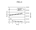
Fig. 4 is a figure showing W/Lg dependency of access resistance Ron and reverse gate current-Igd of each of the conventional structure and the structure according toEmbodiment 1. -
Fig. 5 is a set of figures showing a manufacturing method implemented up to the formation of a buffer layer, a channel layer, a spacer layer, a barrier layer, an insulating film layer, a source electrode, and a drain electrode on a substrate. -
Fig. 6 is a set of figures showing a manufacturing method for forming a gate electrode after the manufacturing method shown inFig. 5 , inEmbodiment 1. -
Fig. 7 is a schematic sectional view showing an example of a structure of a high electron mobility transistor having a nitride semiconductor used therein (GaN HEMT) according toEmbodiment 2. -
Fig. 8 is a schematic sectional view showing an example of a structure of a high electron mobility transistor having a nitride semiconductor used therein (GaN HEMT) according toEmbodiment 3. -
Fig. 9 is a set of figures showing a manufacturing method for forming a gate electrode after the manufacturing method shown inFig. 5 , inEmbodiment 3. - Hereinafter, embodiments of the present invention will be described with reference to the figures.
-
Fig. 2 is a schematic sectional view showing an example of a structure of a high electron mobility transistor having a nitride semiconductor used therein (GaN HEMT) according toEmbodiment 1 of the present invention. Configurations similar to those described in a conventional view (Fig. 1 ) are followed by the same reference numerals, and redundant description will be omitted.Embodiment 1 described below is different from the conventional view (Fig. 1 ) in that there is a portion where anAlN spacer layer 4 is not present. - In
Fig. 2 , Lg10 denotes a horizontal length of a gate electrode 9, and W11 denotes a horizontal length of the portion where thespacer layer 4 is not present. Additionally, Lsd12 denotes a horizontal length between asource electrode 7 and adrain electrode 8. An element isolation region, wirings and the like are actually present, but these are not related to operation of the present invention, and therefore illustration and description thereof will be omitted. - Incidentally, although the GaN HEMT of
Embodiment 1 is utilized as a single amplifier, the present invention is also applicable to a transistor that configures a MMIC (monolithic microwave integrated circuit). - As a
substrate 1, a sapphire, SiC (silicon carbide), Si (silicon), or GaN substrate, or the like is used. Particularly, while a semi-insulating SiC substrate having excellent thermal conductivity is generally utilized, a conventional Si substrate is also often utilized as a semiconductor substrate since the cost is low. - A
buffer layer 2 is a layer inserted between thesubstrate 1 and achannel layer 3, and various structures of AlN, AlGaN, GaN/InGaN, AlN/AlGaN, and a superlattice thereof are used in order to improve the crystalline of thechannel layer 3, and to confine electrons in the channel. - The
channel layer 3 is a layer through which electrons (current) necessary for transistor operation run. As thetypical channel layer 3, GaN is used, InGaN (indium gallium nitride), AlGaN, or a multilayer structure thereof can be also used. - The
spacer layer 4 is inserted between thechannel layer 3 and abarrier layer 5. Thespacer layer 4 is present on the whole surface including thesource electrode 7 and the drain electrode 8 (the whole surface including the vicinity directly below the gate electrode 9) in the conventional structure (Fig. 1 ), but in the structure ofEmbodiment 1 theAlN spacer layer 4 is not present only in a region directly below the gate electrode 9 and in a vicinity of the region. The lateral position of the midpoint of Lg10 coincides with the lateral position of the midpoint of W11. Thisspacer layer 4 is not limited to AlN, and any layer that is larger in polarization than thebarrier layer 5 such as InGaN and AlGaN may be employed. - The
barrier layer 5 forms a two-dimensional electron gas in thechannel layer 3, and therefore is provided above thechannel layer 3, and is a layer containing at least one of In (indium), Al (aluminum) and Ga (gallium), and N (nitrogen). As thisbarrier layer 5, an AlGaN single layer is often used. In addition to this, an advantageous effect of the present invention is obtained when thebarrier layer 5 is constituted by a combination of a plurality of AlGaN matters having different compositions, thicknesses, and impurity concentrations, or a combination of AlGaN and GaN or AlN. - An interface in contact with the
channel layer 3 and theAlN spacer layer 4 is formed by a heterojunction having a wider band gap than thechannel layer 3. Any structure from thesubstrate 1 to thechannel layer 3 is applicable to the present invention. - The
insulating film layer 6 on thebarrier layer 5 serves as a film for suppressing the number of traps on the surface of thebarrier layer 5. A portion where theinsulating film layer 6 is present may be an insulating film containing, as a material, Si that serves as a donor, such as SiN (silicon nitride) and SiO (silicon oxide). When Si is contained, it serves as a donor and supplies electrons to thebarrier layer 5, and the number of traps on the surface of thebarrier layer 5 can be reduced. - The
source electrode 7 and thedrain electrode 8 each are an electrode that extracts a current (electrons) in thechannel layer 3 to the outside of the HEMT. Therefore, thesource electrode 7 and thedrain electrode 8 are formed such that resistance between the electrodes and the two-dimensional electron gas is reduced as much as possible. Thesource electrode 7 and thedrain electrode 8 are formed so as to be in contact with thebarrier layer 5 inFig. 2 , but may be formed so as to be directly in contact with the two-dimensional electron gas (2DEG). Additionally, an n+ region may be formed below thesource electrode 7 and thedrain electrode 8. - The gate electrode 9 is formed so as to contain metal that is in Schottky contact with the
barrier layer 5, and 2DEG concentration below the gate electrode 9 is controlled, thereby implementing a transistor operation. The gate electrode 9 has a gate field plate structure (GFP structure) such that its part protrudes onto the insulatingfilm layer 6. The GFP structure serves as the relaxation of electric field concentration on the surface of thebarrier layer 5. - How a gate leakage current is reduced and reliability is ensured as compared to the conventional structure, and how an effect of reducing access resistance is kept to the same degree as the conventional structure in the structure of the transistor according to
Embodiment 1 are explained below. - As shown in
Fig. 1 , in the conventional structure, anAlN spacer layer 4 is provided over the whole surface between asource electrode 7 and adrain electrode 8. TheAlN spacer layer 4 is larger in polarization than abarrier layer 5, and therefore two-dimensional electron gas concentration in achannel layer 3 can be greater due to the insertion of theAlN spacer layer 4, in comparison with a case where only thebarrier layer 5 is present. - Therefore, it is possible to reduce access resistance that is present between the
source electrode 7 and thedrain electrode 8. On the other hand, when the polarization is increased, an electric field that is concentrated on a gate electrode end is particularly increased. Increase in the electric field in the gate electrode end increases a tunnel current through which electrons runs from a gate electrode 9 toward thebarrier layer 5, and therefore a reverse gate leakage current during OFF-operation increases. The increase in the reverse gate leakage current can be a factor for deteriorating the reliability of the GaN HEMT. - In the structure of the transistor according to
Embodiment 1 of the present invention, as shown inFig. 2 , an electric field in the gate electrode end is reduced by deleting theAlN spacer layer 4 in the region directly below the gate electrode 9 and in the vicinity of the region, which causes the increase in the electric field at the gate electrode end, whereby it is possible to reduce a reverse gate leakage current. Additionally, the length W11 of a portion in which theAlN spacer layer 4 is deleted is sufficiently smaller than the Lsd12 between thesource electrode 7 and thedrain electrode 8, and therefore even when theAlN spacer layer 4 is deleted, it is considered that the effect of reducing the access resistance is maintained at a level substantially identical to that of the conventional structure. - The aforementioned principle is validated by device simulation. In the GaN HEMT having the conventional structure shown in
Fig. 1 , and the GaN HEMT having the structure of theEmbodiment 1 of the present invention shown inFig. 2 , electric fields of portions located below the surface of thebarrier layer 5 by 0.5 nm at a gate voltage of -5 V and at a drain voltage of 30 V were calculated. Thechannel layer 3 was formed of GaN, thespacer layer 4 was formed of AlN, thebarrier layer 5 was formed of AlGaN (Al composition: 0.23). Additionally, the thickness of thechannel layer 3 was set to 1.2 µm, thespacer layer 4 was set to 1 nm, and the thickness of thebarrier layer 5 was set to 20 nm. - In addition, the ratio of the length W11 of the portion in which the
AlN spacer layer 4 is deleted to the gate length Lg10 (W/Lg) in the structure ofEmbodiment 1 of the present invention was set to "2". The polarization of a portion in which theAlN spacer layer 4 is present was set to an average value of the polarization of theAlGaN barrier layer 5 and the polarization of theAlN spacer layer 4, which was 5.27E - 12 cm-3, and the polarization of the portion in which theAlN spacer layer 4 is not present is set to the polarization of theAlGaN barrier layer 5, namely 8.85E - 12 cm-3. -
Fig. 3 is a diagram showing electric fields in gate electrode ends located below the surface of thebarrier layer 5 by 0.5 nm, with respect to the lateral distances (positions from the center of the horizontal direction). As shown inFig. 3 , in the structure ofEmbodiment 1, it is found that an electric field in the vicinity of the gate electrode can be reduced as compared to the conventional structure. -
Fig. 4 is a figure showing W/Lg dependency of access resistance Ron and reverse gate leakage current-Igd of each of the conventional structure and the structure according toEmbodiment 1. Since W = 0 is established in the conventional structure, a value in a case of horizontal axis W/Lg = 0 inFig. 4 shows access resistance Ron in the conventional structure and a reverse gate leakage current -Igd in a case of -Vgd = 100 V. - Then, in the structure according to the
Embodiment 1 of the present invention, as shown inFig. 4 , it is found that the reverse current -Igd is significantly reduced until W/Lg reaches 2, but the reverse current -Igd is gradually saturated when W/Lg becomes larger than 2 (when W doubles Lg). - Further, the access resistance Ron increases, when W/Lg increases. This is because, when W/Lg increases, the length of the portion in which the
AlN spacer layer 4 is present to Lsd12 is reduced, and therefore a two-dimensional electron gas increase effect by the AlN spacer is lowered. When W/Lg is 2, that is, when the horizontal length W11 of the portion in which thespacer layer 4 is not present is twice the horizontal length Lg10 of the gate electrode 9, the portion in which theAlN spacer layer 4 is deleted is the region directly below the gate electrode 9 and the vicinity of the region, and therefore it can be said that the reverse gate leakage current -Igd can be significantly reduced while the increase of the access resistance Ron is suppressed. - Thus far, the structure and its operation in
Embodiment 1 of the present invention are described, and its effectiveness is validated by calculation. Next, a method for manufacturing the GaN HEMT inEmbodiment 1 will be specifically described with reference toFig. 5 andFig. 6 .
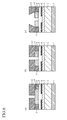
Fig. 5 shows a set of figures showing a manufacturing method up to the formation of thebuffer layer 2, thechannel layer 3, thespacer layer 4, thebarrier layer 5, the insulatingfilm layer 6, thesource electrode 7, and thedrain electrode 8 on thesubstrate 1. In addition,Fig. 6 is a set of figures showing a subsequent manufacturing method for forming the gate electrode 9. - As shown in
Fig. 5(a) , thebuffer layer 2, thechannel layer 3, and thespacer layer 4 are first formed on thesubstrate 1. For these, a MOCVD (metal organic chemical vapor deposition), and/or a MBE (molecular beam epitaxy) can be used. Thespacer layer 4 is not limited to AlN, and any material that is larger in polarization than thebarrier layer 5 may be employed. Such a manufacturing method up to the formation of thespacer layer 4 on thechannel layer 3 is the same as that of the conventional one. - Next, as shown in
Fig. 5(b) , a pattern having an opening in a region in which theAlN spacer layer 4 located in the vicinity of and directly below the gate electrode 9 is removed by photoengraving (photolithography) is formed with a resist 13. That is, the resist 13 is patterned on thespacer layer 4 except the portion in which thespacer layer 4 is to be removed. - Then, while the patterned resist 13 is used as a mask, the
AlN spacer layer 4 in the region to be directly below the gate electrode 9 is removed by etching, and thereafter, the patterned resist 13 is removed. - Next, as shown in
Fig. 5(c) , thebarrier layer 5 is regrown and formed on top of thechannel layer 3 and theAlN spacer layer 4. As this method, the MOCVD can be used. - Further, as shown in
Fig. 5(d) , the insulatingfilm layer 6 is formed on thebarrier layer 5. Although the material of the insulatingfilm layer 6 is typically SiN and SiO, any other materials may be employed as long as the insulatingfilm layer 6 is an insulating film containing Si. - Then, as shown in
Fig. 5(e) , in order to form thesource electrode 7 and thedrain electrode 8, the insulatingfilm layer 6 at portions corresponding to the positions at which thesource electrode 7 or thedrain electrode 8 are formed through a mask such as resist or SiO is removed. Thereafter, metal formation of Ti/Al/Ni/Au, Ti/Al, or the like is performed, and a heat treatment is preformed, whereby thesource electrode 7 and thedrain electrode 8 can be formed. In this process, a heat treatment can also be added thereto by implanting a dopant such as Si ion thereto. - Next, as shown in
Fig. 6(a) , a pattern having an opening in a region to form the gate electrode by photoengraving is formed with a resist 13. That is, the resist 13 is patterned again (re-patterned) on the insulatingfilm layer 6, thesource electrode 7, and thedrain electrode 8 except a portion in which the gate electrode 9 is formed. - Then, as shown in
Fig. 6(b) , after the insulatingfilm layer 6 in the region to form the gate electrode 9 is removed by etching using the re-patterned resist 13 as a mask, the re-patterned resist 13 is removed. - Next, as shown in
Fig. 6(c) , a pattern having a larger opening than the region etched inFig. 6(b) is formed with a resist 13 such that gate electrode 9 is formed also on the insulatingfilm layer 6 by photoengraving. That is, the resist 13 having the larger opening than the region in which the insulatingfilm layer 6 is removed by etching is finally patterned. - Thereafter, the gate electrode 9 is formed on the region in which the insulating
film layer 6 is removed by etching, and the insulatingfilm layer 6, and the finally patterned resist is removed. Specifically, metal having Schottky characteristics is deposited (EB (electron beam) vapor deposition or sputtering can be used), the resist 13 is removed (lifted off), whereby it is possible to form the structure as shown inFig. 2 . Finally, a protective film, wiring, via hole wiring, capacity, resistance, or the like is produced as needed, but illustration and description thereof will be omitted here. - As described above, according to
Embodiment 1, the AlN spacer layer is not present in the region directly below the gate electrode and in the vicinity of the region, and therefore the electric field at the gate electrode end is smaller than that of the transistor having the conventional structure, and the gate leakage current is reduced and reliability is secured. Additionally, the length of the portion in which the AlN spacer layer is not present is sufficiently smaller than the distance between the source electrode and the drain electrode, and therefore reduction in access resistance by the AlN spacer layer can be kept to the same degree as the conventional structure, and increase in access resistance can be suppressed. -
Fig. 7 is a schematic sectional view showing an example of a structure of a high electron mobility transistor having a nitride semiconductor used therein (GaN HEMT) according toEmbodiment 2 of the present invention. Note that components similar to those described in the conventional view (Fig. 1 ) andEmbodiment 1 are denoted by the same reference numerals, and redundant description thereof will be omitted. A structure of a gate electrode 9 ofEmbodiment 2 described below is different from that ofEmbodiment 1 in that the gate electrode 9 on the insulatingfilm layer 6 has a two-tiered structure. - In this way, the gate electrode 9 is configured to be two-tiered, whereby the number of edges increases, and therefore an advantageous effect of dispersing an electric field that is concentrated at a gate electrode end is enhanced. Therefore, a larger electric field reduction than the case of
Embodiment 1 becomes possible, a reverse gate leakage current is reduced, and furthermore, reliability is improved. - Also in the GaN HEMT of
Embodiment 2, a manufacturing method up to the formation of abuffer layer 2, achannel layer 3, aspacer layer 4, abarrier layer 5, the insulatingfilm layer 6, asource electrode 7, and adrain electrode 8 on asubstrate 1 is the same as the method described inEmbodiment 1 with reference toFig. 6 . - Next, as shown in
Fig. 6(a) , the formation of a pattern having an opening on a region that becomes the gate electrode by photoengraving, with a resist 13 is the same as that ofEmbodiment 1. - In this connection, in a case where the structure shown in
Fig. 7 is formed, two kinds of insulating films whose etching rates of wet etching are different need to be formed when the insulatingfilm layer 6 is formed. An insulating film whose etching rate is low of the two kinds of insulating film is disposed in a lower layer, and an insulating film whose etching rate is high is disposed in an upper layer, thereby forming a double-layer structure. As such a method for forming the double-layer structure, there are various methods such as cat-CVD (catalytic chemical vapor deposition), plasma CVD, and sputtering. - In this way, in order to form the insulating
film layer 6 so as to have the double-layer structure in which the etching rates are different, as shown inFig. 6(b) , after the insulatingfilm layer 6 in a region to form the gate electrode is etched, only the upper layer is wet-etched before the resist 13 is removed. The etching rate of the upper layer of the two layers of the insulatingfilm layer 6 is high, and therefore etching portions of the side surfaces can be configured to be two-tiered, and the insulatingfilm layer 6 having the double-layer structure inEmbodiment 2 can be formed. - Thereafter, after the resist 13 is removed, a pattern having a larger opening than the region etched in
Fig. 6(b) is formed with a resist 13 such that the gate electrode 9 is formed also on the insulatingfilm layer 6 by photoengraving, as shown inFig. 6(c) . - Then, metal having Schottky characteristics is deposited (EB (electron beam) vapor deposition or sputtering can be used), the resist 13 is removed (lifted off), whereby it is possible to form the structure as shown in
Fig. 7 . Finally, a protective film, wiring, via hole wiring, capacity, resistance, or the like is produced as needed, but illustration and description thereof will be omitted. - As described above, according to
Embodiment 2, the gate electrode has the two-tiered structure, whereby the number of edges increases, and the advantageous effect of dispersing the electric field that is concentrated at the gate electrode end is enhanced. Therefore, larger electric field reduction as compared to the transistor ofEmbodiment 1 becomes possible, a reverse gate leakage current is reduced, and furthermore, reliability is improved. -
Fig. 8 is a schematic sectional view showing an example of a structure of a high electron mobility transistor having a nitride semiconductor used therein (GaN HEMT) according toEmbodiment 3 of the present invention. Note that components similar to those described in the conventional view (Fig. 1 ) and Embodiments 1 and 2 are denoted by the same reference numerals, and redundant description thereof will be omitted. A structure of a gate electrode 9 ofEmbodiment 3 described below is different from that ofEmbodiment 1 in that the gate electrode 9 on an insulatingfilm layer 6 has an inclined structure. - In this way, the gate electrode 9 is inclined, whereby an electric field is averaged, and therefore it is possible to reduce an electric field that is concentrated at a gate electrode end. Therefore, electric field reduction can be implemented at a greater level than that of the case of
Embodiment 1, a reverse gate leakage current is reduced, and furthermore, reliability is improved. - Also in the GaN HEMT of
Embodiment 3, a manufacturing method up to the formation of abuffer layer 2, achannel layer 3, aspacer layer 4, abarrier layer 5, the insulatingfilm layer 6, asource electrode 7, and adrain electrode 8 on asubstrate 1 is the same as the method described inEmbodiment 1 with reference toFig. 5 . -
Fig. 9 is a set of figures showing a manufacturing method for forming the gate electrode 9 after the manufacturing method shown inFig. 5 , inEmbodiment 3. - As shown in
Fig. 9(a) , a pattern having an opening on a region to form the gate electrode by photoengraving is formed with a resist 13. - Then, as shown in
Fig. 9(b) , after side surfaces of an etching portion are inclined depending on an etching condition at this time, and the insulatingfilm layer 6 in the region that becomes the gate electrode is removed by etching, the resist 13 is removed. - Thereafter, as shown in
Fig. 6(c) , a pattern having a larger opening than the region etched inFig. 9(b) is formed with a resist 13 such that the gate electrode 9 is formed also on the insulatingfilm layer 6 by photoengraving. - Then, metal having Schottky characteristics is deposited (EB (electron beam) vapor deposition or sputtering can be used), the resist 13 is removed (lifted off), whereby it is possible to form the structure as shown in
Fig. 8 . Finally, a protective film, wiring, via hole wiring, capacity, resistance, or the like is produced as needed, but illustration and description thereof will be omitted. - As described above, according to
Embodiment 3, the side surfaces of the gate electrode are inclined, whereby an electric field is averaged, and it is possible to reduce the electric field that is concentrated at the gate electrode end. Therefore, larger electric field reduction as compared to the transistor ofEmbodiment 1 is possible, a reverse gate leakage current is reduced, and furthermore, reliability is improved. - Incidentally, the present invention can be implemented by free combination of the respective embodiments, modification of arbitrary components of the respective embodiments, or omission of arbitrary components of the respective embodiments, within the scope of the invention.
- A transistor having a nitride semiconductor used therein of the present invention, and a method for manufacturing a transistor having a nitride semiconductor used therein are applicable to an amplifier or a power switch circuit.
-
- 1: SUBSTRATE
- 2: BUFFER LAYER
- 3: CHANNEL LAYER
- 4: SPACER LAYER
- 5: BARRIER LAYER
- 6: INSULATING FILM LAYER
- 7: SOURCE ELECTRODE
- 8: DRAIN ELECTRODE
- 9: GATE ELECTRODE
- 10: LENGTH OF GATE ELECTRODE 9 (Lg)
- 11: LENGTH OF PORTION WHERE
SPACER LAYER 4 IS NOT PRESENT (W) - 12: LENGTH BETWEEN
SOURCE ELECTRODE 7 AND DRAIN ELECTRODE 8 (Lsd) - 13: RESIST.
Claims (6)
- A transistor having a nitride semiconductor used therein, comprising: a channel layer through which electrons run; a barrier layer that forms a two-dimensional electron gas in the channel layer and that is provided above the channel layer and contains at least one of indium, aluminum and gallium, and nitrogen; and a gate electrode, a source electrode, and a drain electrode that are arranged on the barrier layer,
the transistor further comprising
a spacer layer that is inserted between the barrier layer and the channel layer, and that is larger in polarization than the barrier layer, wherein
the spacer layer is not present only in a region directly below the gate electrode and in a vicinity of the region. - The transistor according to claim 1, wherein the spacer layer is formed of aluminum nitride.
- The transistor according to claim 1, wherein a horizontal length of a portion where the spacer layer is not present is twice a horizontal length of the gate electrode.
- The transistor according to claim 1, wherein the gate electrode has a two-tiered structure.
- The transistor according to claim 1, wherein a side surface of the gate electrode is inclined.
- A method for manufacturing a transistor having a nitride semiconductor used therein, the transistor including: a channel layer through which electrons run; a barrier layer that forms a two-dimensional electron gas in the channel layer and that is provided above the channel layer and contains at least one of indium, aluminum and gallium, and nitrogen; and a gate electrode, a source electrode, and a drain electrode that are arranged on the barrier layer,
the method comprising:a step of forming a spacer layer that is larger in polarization than the barrier layer, on the channel layer;a step of patterning a resist on the spacer layer except a portion where the spacer layer is removed;a step of removing by etching the spacer layer in a region to be directly below the gate electrode using the patterned resist as a mask;a step of removing the patterned resist;a step of forming the barrier layer on top of the channel layer and the spacer layer;a step of forming an insulating film layer on the barrier layer;a step of removing the insulating film layer corresponding to positions to be formed by the source electrode and the drain electrode, and then forming the source electrode and the drain electrode;a step of re-patterning a resist on the insulating film layer, the source electrode, and the drain electrode except a portion where the gate electrode is formed;a step of removing by etching the insulating film layer in a region to form the gate electrode using the re-patterned resist as a mask;a step of removing the re-patterned resist;a step of finally patterning a resist having a larger opening than a region where the insulating film layer is removed by etching;a step of forming the gate electrode on the region where the insulating film layer is removed by etching, and on the insulating film layer; anda step of removing the finally patterned resist.
Applications Claiming Priority (1)
| Application Number | Priority Date | Filing Date | Title |
|---|---|---|---|
| PCT/JP2012/082660 WO2014097369A1 (en) | 2012-12-17 | 2012-12-17 | Transistor having nitride semiconductor used therein and method for manufacturing transistor having nitride semiconductor used therein |
Publications (3)
| Publication Number | Publication Date |
|---|---|
| EP2933827A1 true EP2933827A1 (en) | 2015-10-21 |
| EP2933827A4 EP2933827A4 (en) | 2016-10-26 |
| EP2933827B1 EP2933827B1 (en) | 2021-09-15 |
Family
ID=50977758
Family Applications (1)
| Application Number | Title | Priority Date | Filing Date |
|---|---|---|---|
| EP12890237.6A Active EP2933827B1 (en) | 2012-12-17 | 2012-12-17 | Transistor having nitride semiconductor used therein and method for manufacturing transistor having nitride semiconductor used therein |
Country Status (4)
| Country | Link |
|---|---|
| US (1) | US9570599B2 (en) |
| EP (1) | EP2933827B1 (en) |
| JP (1) | JP5744346B2 (en) |
| WO (1) | WO2014097369A1 (en) |
Families Citing this family (4)
| Publication number | Priority date | Publication date | Assignee | Title |
|---|---|---|---|---|
| US9761438B1 (en) * | 2014-05-08 | 2017-09-12 | Hrl Laboratories, Llc | Method for manufacturing a semiconductor structure having a passivated III-nitride layer |
| US9780176B2 (en) | 2015-11-05 | 2017-10-03 | Electronics And Telecommunications Research Institute | High reliability field effect power device and manufacturing method thereof |
| US10608102B2 (en) * | 2017-09-29 | 2020-03-31 | Electronics And Telecommunications Research Institute | Semiconductor device having a drain electrode contacting an epi material inside a through-hole and method of manufacturing the same |
| US12581701B2 (en) * | 2021-10-18 | 2026-03-17 | Globalfoundries U.S. Inc. | Device with dual isolation structure |
Family Cites Families (10)
| Publication number | Priority date | Publication date | Assignee | Title |
|---|---|---|---|---|
| JP3372470B2 (en) | 1998-01-20 | 2003-02-04 | シャープ株式会社 | Nitride III-V compound semiconductor device |
| US7030428B2 (en) * | 2001-12-03 | 2006-04-18 | Cree, Inc. | Strain balanced nitride heterojunction transistors |
| JP4865189B2 (en) * | 2002-02-21 | 2012-02-01 | 古河電気工業株式会社 | GaN-based field effect transistor |
| JP2006286698A (en) | 2005-03-31 | 2006-10-19 | Furukawa Electric Co Ltd:The | Electronic device and power converter |
| JP2008306130A (en) * | 2007-06-11 | 2008-12-18 | Sanken Electric Co Ltd | Field effect semiconductor device and method for manufacturing the same |
| JP5348364B2 (en) * | 2007-08-27 | 2013-11-20 | サンケン電気株式会社 | Heterojunction field effect semiconductor device |
| JP2009099691A (en) | 2007-10-15 | 2009-05-07 | Sanken Electric Co Ltd | Method of manufacturing field-effect semiconductor device |
| JP5339718B2 (en) * | 2007-12-20 | 2013-11-13 | 三菱電機株式会社 | Heterojunction field effect transistor and method of manufacturing the same |
| JP4794656B2 (en) * | 2009-06-11 | 2011-10-19 | シャープ株式会社 | Semiconductor device |
| WO2010151721A1 (en) * | 2009-06-25 | 2010-12-29 | The Government Of The United States Of America, As Represented By The Secretary Of The Navy | Transistor with enhanced channel charge inducing material layer and threshold voltage control |
-
2012
- 2012-12-17 WO PCT/JP2012/082660 patent/WO2014097369A1/en not_active Ceased
- 2012-12-17 EP EP12890237.6A patent/EP2933827B1/en active Active
- 2012-12-17 JP JP2014552768A patent/JP5744346B2/en not_active Expired - Fee Related
- 2012-12-17 US US14/427,960 patent/US9570599B2/en active Active
Also Published As
| Publication number | Publication date |
|---|---|
| EP2933827A4 (en) | 2016-10-26 |
| JP5744346B2 (en) | 2015-07-08 |
| WO2014097369A1 (en) | 2014-06-26 |
| JPWO2014097369A1 (en) | 2017-01-12 |
| EP2933827B1 (en) | 2021-09-15 |
| US20150249150A1 (en) | 2015-09-03 |
| US9570599B2 (en) | 2017-02-14 |
Similar Documents
| Publication | Publication Date | Title |
|---|---|---|
| EP1665358B1 (en) | Fabrication of single or multiple gate field plates | |
| JP5564815B2 (en) | Semiconductor device and manufacturing method of semiconductor device | |
| US8330167B2 (en) | GaN-based field effect transistor and method of manufacturing the same | |
| JP5707786B2 (en) | Compound semiconductor device and manufacturing method thereof | |
| KR101357477B1 (en) | Compound semiconductor device, and method for manufacturing the same | |
| US10283632B2 (en) | Nitride semiconductor device and manufacturing method thereof | |
| EP2955755B1 (en) | Nitride high-voltage component and manufacturing method therefor | |
| CN103887334B (en) | GaN high electron mobility transistor and GaN diode | |
| EP3549173B1 (en) | High electron mobility transistor and method for manufacturing high electron mobility transistor | |
| JPWO2006080109A1 (en) | Semiconductor device having MIS structure and manufacturing method thereof | |
| JP2010192633A (en) | METHOD FOR MANUFACTURING GaN-BASED FIELD-EFFECT TRANSISTOR | |
| US10312175B1 (en) | Diamond air bridge for thermal management of high power devices | |
| JP6199147B2 (en) | Field effect type compound semiconductor device and manufacturing method thereof | |
| JP6905197B2 (en) | Compound semiconductor device and its manufacturing method | |
| US12336254B2 (en) | Semiconductor device with conductive elements formed over dielectric layers and method of fabrication therefor | |
| CN103715243A (en) | Compound semiconductor device and manufacturing method thereof | |
| JP2014017423A (en) | Compound semiconductor device and method for manufacturing the same | |
| CN103700700A (en) | Compound semiconductor device and method of manufacturing the same | |
| US10373833B2 (en) | Semiconductor device and method for manufacturing the same | |
| CN106257686A (en) | Semiconductor device and manufacture method thereof | |
| US9570599B2 (en) | Transistor having nitride semiconductor used therein and method for manufacturing transistor having nitride semiconductor used therein | |
| WO2007007589A1 (en) | Field effect transistor and method for manufacturing same | |
| EP3405979B1 (en) | Semiconductor device, electronic part, electronic apparatus, and method for fabricating semiconductor device | |
| WO2007041595A2 (en) | Iii-nitride semiconductor fabrication | |
| JP2016086108A (en) | Compound semiconductor device |
Legal Events
| Date | Code | Title | Description |
|---|---|---|---|
| PUAI | Public reference made under article 153(3) epc to a published international application that has entered the european phase |
Free format text: ORIGINAL CODE: 0009012 |
|
| 17P | Request for examination filed |
Effective date: 20150226 |
|
| AK | Designated contracting states |
Kind code of ref document: A1 Designated state(s): AL AT BE BG CH CY CZ DE DK EE ES FI FR GB GR HR HU IE IS IT LI LT LU LV MC MK MT NL NO PL PT RO RS SE SI SK SM TR |
|
| AX | Request for extension of the european patent |
Extension state: BA ME |
|
| DAX | Request for extension of the european patent (deleted) | ||
| A4 | Supplementary search report drawn up and despatched |
Effective date: 20160928 |
|
| RIC1 | Information provided on ipc code assigned before grant |
Ipc: H01L 29/423 20060101ALN20160922BHEP Ipc: H01L 21/338 20060101ALI20160922BHEP Ipc: H01L 29/20 20060101ALN20160922BHEP Ipc: H01L 29/778 20060101AFI20160922BHEP Ipc: H01L 29/10 20060101ALI20160922BHEP |
|
| STAA | Information on the status of an ep patent application or granted ep patent |
Free format text: STATUS: EXAMINATION IS IN PROGRESS |
|
| 17Q | First examination report despatched |
Effective date: 20170627 |
|
| REG | Reference to a national code |
Ref country code: DE Ref legal event code: R079 Ref document number: 602012076715 Country of ref document: DE Free format text: PREVIOUS MAIN CLASS: H01L0021338000 Ipc: H01L0029778000 |
|
| GRAP | Despatch of communication of intention to grant a patent |
Free format text: ORIGINAL CODE: EPIDOSNIGR1 |
|
| STAA | Information on the status of an ep patent application or granted ep patent |
Free format text: STATUS: GRANT OF PATENT IS INTENDED |
|
| RIC1 | Information provided on ipc code assigned before grant |
Ipc: H01L 29/423 20060101ALN20210310BHEP Ipc: H01L 29/20 20060101ALN20210310BHEP Ipc: H01L 29/10 20060101ALI20210310BHEP Ipc: H01L 21/338 20060101ALI20210310BHEP Ipc: H01L 29/778 20060101AFI20210310BHEP |
|
| RIC1 | Information provided on ipc code assigned before grant |
Ipc: H01L 29/423 20060101ALN20210325BHEP Ipc: H01L 29/20 20060101ALN20210325BHEP Ipc: H01L 29/10 20060101ALI20210325BHEP Ipc: H01L 21/338 20060101ALI20210325BHEP Ipc: H01L 29/778 20060101AFI20210325BHEP |
|
| INTG | Intention to grant announced |
Effective date: 20210409 |
|
| GRAS | Grant fee paid |
Free format text: ORIGINAL CODE: EPIDOSNIGR3 |
|
| GRAA | (expected) grant |
Free format text: ORIGINAL CODE: 0009210 |
|
| STAA | Information on the status of an ep patent application or granted ep patent |
Free format text: STATUS: THE PATENT HAS BEEN GRANTED |
|
| AK | Designated contracting states |
Kind code of ref document: B1 Designated state(s): AL AT BE BG CH CY CZ DE DK EE ES FI FR GB GR HR HU IE IS IT LI LT LU LV MC MK MT NL NO PL PT RO RS SE SI SK SM TR |
|
| REG | Reference to a national code |
Ref country code: CH Ref legal event code: EP Ref country code: GB Ref legal event code: FG4D |
|
| REG | Reference to a national code |
Ref country code: DE Ref legal event code: R096 Ref document number: 602012076715 Country of ref document: DE |
|
| REG | Reference to a national code |
Ref country code: IE Ref legal event code: FG4D |
|
| REG | Reference to a national code |
Ref country code: AT Ref legal event code: REF Ref document number: 1431199 Country of ref document: AT Kind code of ref document: T Effective date: 20211015 |
|
| REG | Reference to a national code |
Ref country code: LT Ref legal event code: MG9D |
|
| REG | Reference to a national code |
Ref country code: NL Ref legal event code: MP Effective date: 20210915 |
|
| PG25 | Lapsed in a contracting state [announced via postgrant information from national office to epo] |
Ref country code: RS Free format text: LAPSE BECAUSE OF FAILURE TO SUBMIT A TRANSLATION OF THE DESCRIPTION OR TO PAY THE FEE WITHIN THE PRESCRIBED TIME-LIMIT Effective date: 20210915 Ref country code: NO Free format text: LAPSE BECAUSE OF FAILURE TO SUBMIT A TRANSLATION OF THE DESCRIPTION OR TO PAY THE FEE WITHIN THE PRESCRIBED TIME-LIMIT Effective date: 20211215 Ref country code: FI Free format text: LAPSE BECAUSE OF FAILURE TO SUBMIT A TRANSLATION OF THE DESCRIPTION OR TO PAY THE FEE WITHIN THE PRESCRIBED TIME-LIMIT Effective date: 20210915 Ref country code: BG Free format text: LAPSE BECAUSE OF FAILURE TO SUBMIT A TRANSLATION OF THE DESCRIPTION OR TO PAY THE FEE WITHIN THE PRESCRIBED TIME-LIMIT Effective date: 20211215 Ref country code: LT Free format text: LAPSE BECAUSE OF FAILURE TO SUBMIT A TRANSLATION OF THE DESCRIPTION OR TO PAY THE FEE WITHIN THE PRESCRIBED TIME-LIMIT Effective date: 20210915 Ref country code: HR Free format text: LAPSE BECAUSE OF FAILURE TO SUBMIT A TRANSLATION OF THE DESCRIPTION OR TO PAY THE FEE WITHIN THE PRESCRIBED TIME-LIMIT Effective date: 20210915 Ref country code: SE Free format text: LAPSE BECAUSE OF FAILURE TO SUBMIT A TRANSLATION OF THE DESCRIPTION OR TO PAY THE FEE WITHIN THE PRESCRIBED TIME-LIMIT Effective date: 20210915 |
|
| REG | Reference to a national code |
Ref country code: AT Ref legal event code: MK05 Ref document number: 1431199 Country of ref document: AT Kind code of ref document: T Effective date: 20210915 |
|
| PG25 | Lapsed in a contracting state [announced via postgrant information from national office to epo] |
Ref country code: LV Free format text: LAPSE BECAUSE OF FAILURE TO SUBMIT A TRANSLATION OF THE DESCRIPTION OR TO PAY THE FEE WITHIN THE PRESCRIBED TIME-LIMIT Effective date: 20210915 Ref country code: GR Free format text: LAPSE BECAUSE OF FAILURE TO SUBMIT A TRANSLATION OF THE DESCRIPTION OR TO PAY THE FEE WITHIN THE PRESCRIBED TIME-LIMIT Effective date: 20211216 |
|
| PG25 | Lapsed in a contracting state [announced via postgrant information from national office to epo] |
Ref country code: AT Free format text: LAPSE BECAUSE OF FAILURE TO SUBMIT A TRANSLATION OF THE DESCRIPTION OR TO PAY THE FEE WITHIN THE PRESCRIBED TIME-LIMIT Effective date: 20210915 |
|
| PG25 | Lapsed in a contracting state [announced via postgrant information from national office to epo] |
Ref country code: IS Free format text: LAPSE BECAUSE OF FAILURE TO SUBMIT A TRANSLATION OF THE DESCRIPTION OR TO PAY THE FEE WITHIN THE PRESCRIBED TIME-LIMIT Effective date: 20220115 Ref country code: SM Free format text: LAPSE BECAUSE OF FAILURE TO SUBMIT A TRANSLATION OF THE DESCRIPTION OR TO PAY THE FEE WITHIN THE PRESCRIBED TIME-LIMIT Effective date: 20210915 Ref country code: SK Free format text: LAPSE BECAUSE OF FAILURE TO SUBMIT A TRANSLATION OF THE DESCRIPTION OR TO PAY THE FEE WITHIN THE PRESCRIBED TIME-LIMIT Effective date: 20210915 Ref country code: RO Free format text: LAPSE BECAUSE OF FAILURE TO SUBMIT A TRANSLATION OF THE DESCRIPTION OR TO PAY THE FEE WITHIN THE PRESCRIBED TIME-LIMIT Effective date: 20210915 Ref country code: PT Free format text: LAPSE BECAUSE OF FAILURE TO SUBMIT A TRANSLATION OF THE DESCRIPTION OR TO PAY THE FEE WITHIN THE PRESCRIBED TIME-LIMIT Effective date: 20220117 Ref country code: PL Free format text: LAPSE BECAUSE OF FAILURE TO SUBMIT A TRANSLATION OF THE DESCRIPTION OR TO PAY THE FEE WITHIN THE PRESCRIBED TIME-LIMIT Effective date: 20210915 Ref country code: NL Free format text: LAPSE BECAUSE OF FAILURE TO SUBMIT A TRANSLATION OF THE DESCRIPTION OR TO PAY THE FEE WITHIN THE PRESCRIBED TIME-LIMIT Effective date: 20210915 Ref country code: ES Free format text: LAPSE BECAUSE OF FAILURE TO SUBMIT A TRANSLATION OF THE DESCRIPTION OR TO PAY THE FEE WITHIN THE PRESCRIBED TIME-LIMIT Effective date: 20210915 Ref country code: EE Free format text: LAPSE BECAUSE OF FAILURE TO SUBMIT A TRANSLATION OF THE DESCRIPTION OR TO PAY THE FEE WITHIN THE PRESCRIBED TIME-LIMIT Effective date: 20210915 Ref country code: CZ Free format text: LAPSE BECAUSE OF FAILURE TO SUBMIT A TRANSLATION OF THE DESCRIPTION OR TO PAY THE FEE WITHIN THE PRESCRIBED TIME-LIMIT Effective date: 20210915 Ref country code: AL Free format text: LAPSE BECAUSE OF FAILURE TO SUBMIT A TRANSLATION OF THE DESCRIPTION OR TO PAY THE FEE WITHIN THE PRESCRIBED TIME-LIMIT Effective date: 20210915 |
|
| REG | Reference to a national code |
Ref country code: DE Ref legal event code: R097 Ref document number: 602012076715 Country of ref document: DE |
|
| PLBE | No opposition filed within time limit |
Free format text: ORIGINAL CODE: 0009261 |
|
| STAA | Information on the status of an ep patent application or granted ep patent |
Free format text: STATUS: NO OPPOSITION FILED WITHIN TIME LIMIT |
|
| PG25 | Lapsed in a contracting state [announced via postgrant information from national office to epo] |
Ref country code: MC Free format text: LAPSE BECAUSE OF FAILURE TO SUBMIT A TRANSLATION OF THE DESCRIPTION OR TO PAY THE FEE WITHIN THE PRESCRIBED TIME-LIMIT Effective date: 20210915 Ref country code: DK Free format text: LAPSE BECAUSE OF FAILURE TO SUBMIT A TRANSLATION OF THE DESCRIPTION OR TO PAY THE FEE WITHIN THE PRESCRIBED TIME-LIMIT Effective date: 20210915 |
|
| REG | Reference to a national code |
Ref country code: CH Ref legal event code: PL |
|
| 26N | No opposition filed |
Effective date: 20220616 |
|
| PG25 | Lapsed in a contracting state [announced via postgrant information from national office to epo] |
Ref country code: SI Free format text: LAPSE BECAUSE OF FAILURE TO SUBMIT A TRANSLATION OF THE DESCRIPTION OR TO PAY THE FEE WITHIN THE PRESCRIBED TIME-LIMIT Effective date: 20210915 |
|
| REG | Reference to a national code |
Ref country code: BE Ref legal event code: MM Effective date: 20211231 |
|
| PG25 | Lapsed in a contracting state [announced via postgrant information from national office to epo] |
Ref country code: LU Free format text: LAPSE BECAUSE OF NON-PAYMENT OF DUE FEES Effective date: 20211217 Ref country code: IE Free format text: LAPSE BECAUSE OF NON-PAYMENT OF DUE FEES Effective date: 20211217 |
|
| PG25 | Lapsed in a contracting state [announced via postgrant information from national office to epo] |
Ref country code: BE Free format text: LAPSE BECAUSE OF NON-PAYMENT OF DUE FEES Effective date: 20211231 |
|
| PG25 | Lapsed in a contracting state [announced via postgrant information from national office to epo] |
Ref country code: LI Free format text: LAPSE BECAUSE OF NON-PAYMENT OF DUE FEES Effective date: 20211231 Ref country code: CH Free format text: LAPSE BECAUSE OF NON-PAYMENT OF DUE FEES Effective date: 20211231 |
|
| PG25 | Lapsed in a contracting state [announced via postgrant information from national office to epo] |
Ref country code: IT Free format text: LAPSE BECAUSE OF FAILURE TO SUBMIT A TRANSLATION OF THE DESCRIPTION OR TO PAY THE FEE WITHIN THE PRESCRIBED TIME-LIMIT Effective date: 20210915 |
|
| PG25 | Lapsed in a contracting state [announced via postgrant information from national office to epo] |
Ref country code: HU Free format text: LAPSE BECAUSE OF FAILURE TO SUBMIT A TRANSLATION OF THE DESCRIPTION OR TO PAY THE FEE WITHIN THE PRESCRIBED TIME-LIMIT; INVALID AB INITIO Effective date: 20121217 Ref country code: CY Free format text: LAPSE BECAUSE OF FAILURE TO SUBMIT A TRANSLATION OF THE DESCRIPTION OR TO PAY THE FEE WITHIN THE PRESCRIBED TIME-LIMIT Effective date: 20210915 |
|
| P01 | Opt-out of the competence of the unified patent court (upc) registered |
Effective date: 20230512 |
|
| REG | Reference to a national code |
Ref country code: DE Ref legal event code: R084 Ref document number: 602012076715 Country of ref document: DE |
|
| PG25 | Lapsed in a contracting state [announced via postgrant information from national office to epo] |
Ref country code: MK Free format text: LAPSE BECAUSE OF FAILURE TO SUBMIT A TRANSLATION OF THE DESCRIPTION OR TO PAY THE FEE WITHIN THE PRESCRIBED TIME-LIMIT Effective date: 20210915 |
|
| REG | Reference to a national code |
Ref country code: GB Ref legal event code: 746 Effective date: 20240605 |
|
| PG25 | Lapsed in a contracting state [announced via postgrant information from national office to epo] |
Ref country code: TR Free format text: LAPSE BECAUSE OF FAILURE TO SUBMIT A TRANSLATION OF THE DESCRIPTION OR TO PAY THE FEE WITHIN THE PRESCRIBED TIME-LIMIT Effective date: 20210915 |
|
| PG25 | Lapsed in a contracting state [announced via postgrant information from national office to epo] |
Ref country code: MT Free format text: LAPSE BECAUSE OF FAILURE TO SUBMIT A TRANSLATION OF THE DESCRIPTION OR TO PAY THE FEE WITHIN THE PRESCRIBED TIME-LIMIT Effective date: 20210915 |
|
| REG | Reference to a national code |
Ref country code: DE Ref legal event code: R079 Ref document number: 602012076715 Country of ref document: DE Free format text: PREVIOUS MAIN CLASS: H01L0029778000 Ipc: H10D0030470000 |
|
| PGFP | Annual fee paid to national office [announced via postgrant information from national office to epo] |
Ref country code: DE Payment date: 20251028 Year of fee payment: 14 |
|
| PGFP | Annual fee paid to national office [announced via postgrant information from national office to epo] |
Ref country code: GB Payment date: 20251030 Year of fee payment: 14 |
|
| PGFP | Annual fee paid to national office [announced via postgrant information from national office to epo] |
Ref country code: FR Payment date: 20251117 Year of fee payment: 14 |