EP2931007B1 - Microwave processing device - Google Patents
Microwave processing device Download PDFInfo
- Publication number
- EP2931007B1 EP2931007B1 EP13860191.9A EP13860191A EP2931007B1 EP 2931007 B1 EP2931007 B1 EP 2931007B1 EP 13860191 A EP13860191 A EP 13860191A EP 2931007 B1 EP2931007 B1 EP 2931007B1
- Authority
- EP
- European Patent Office
- Prior art keywords
- periodic structure
- structure body
- impedance
- processing device
- matching part
- Prior art date
- Legal status (The legal status is an assumption and is not a legal conclusion. Google has not performed a legal analysis and makes no representation as to the accuracy of the status listed.)
- Active
Links
- 230000000737 periodic effect Effects 0.000 claims description 106
- 230000005540 biological transmission Effects 0.000 claims description 27
- 239000004020 conductor Substances 0.000 claims description 17
- 238000010438 heat treatment Methods 0.000 description 9
- 238000010276 construction Methods 0.000 description 2
- 238000010411 cooking Methods 0.000 description 2
- 230000000694 effects Effects 0.000 description 2
- 230000005684 electric field Effects 0.000 description 2
- 239000000463 material Substances 0.000 description 2
- 238000012986 modification Methods 0.000 description 2
- 230000004048 modification Effects 0.000 description 2
- 230000001105 regulatory effect Effects 0.000 description 2
- 239000012141 concentrate Substances 0.000 description 1
- 238000001816 cooling Methods 0.000 description 1
- 238000000034 method Methods 0.000 description 1
- 239000004065 semiconductor Substances 0.000 description 1
- 239000011800 void material Substances 0.000 description 1
Images


Classifications
-
- H—ELECTRICITY
- H03—ELECTRONIC CIRCUITRY
- H03H—IMPEDANCE NETWORKS, e.g. RESONANT CIRCUITS; RESONATORS
- H03H7/00—Multiple-port networks comprising only passive electrical elements as network components
- H03H7/38—Impedance-matching networks
-
- H—ELECTRICITY
- H05—ELECTRIC TECHNIQUES NOT OTHERWISE PROVIDED FOR
- H05B—ELECTRIC HEATING; ELECTRIC LIGHT SOURCES NOT OTHERWISE PROVIDED FOR; CIRCUIT ARRANGEMENTS FOR ELECTRIC LIGHT SOURCES, IN GENERAL
- H05B6/00—Heating by electric, magnetic or electromagnetic fields
- H05B6/64—Heating using microwaves
- H05B6/70—Feed lines
-
- H—ELECTRICITY
- H05—ELECTRIC TECHNIQUES NOT OTHERWISE PROVIDED FOR
- H05B—ELECTRIC HEATING; ELECTRIC LIGHT SOURCES NOT OTHERWISE PROVIDED FOR; CIRCUIT ARRANGEMENTS FOR ELECTRIC LIGHT SOURCES, IN GENERAL
- H05B6/00—Heating by electric, magnetic or electromagnetic fields
- H05B6/64—Heating using microwaves
- H05B6/6408—Supports or covers specially adapted for use in microwave heating apparatus
-
- H—ELECTRICITY
- H05—ELECTRIC TECHNIQUES NOT OTHERWISE PROVIDED FOR
- H05B—ELECTRIC HEATING; ELECTRIC LIGHT SOURCES NOT OTHERWISE PROVIDED FOR; CIRCUIT ARRANGEMENTS FOR ELECTRIC LIGHT SOURCES, IN GENERAL
- H05B6/00—Heating by electric, magnetic or electromagnetic fields
- H05B6/64—Heating using microwaves
- H05B6/647—Aspects related to microwave heating combined with other heating techniques
- H05B6/6491—Aspects related to microwave heating combined with other heating techniques combined with the use of susceptors
- H05B6/6494—Aspects related to microwave heating combined with other heating techniques combined with the use of susceptors for cooking
-
- H—ELECTRICITY
- H05—ELECTRIC TECHNIQUES NOT OTHERWISE PROVIDED FOR
- H05B—ELECTRIC HEATING; ELECTRIC LIGHT SOURCES NOT OTHERWISE PROVIDED FOR; CIRCUIT ARRANGEMENTS FOR ELECTRIC LIGHT SOURCES, IN GENERAL
- H05B6/00—Heating by electric, magnetic or electromagnetic fields
- H05B6/64—Heating using microwaves
- H05B6/66—Circuits
- H05B6/662—Aspects related to the boost transformer of the microwave heating apparatus
-
- H—ELECTRICITY
- H05—ELECTRIC TECHNIQUES NOT OTHERWISE PROVIDED FOR
- H05B—ELECTRIC HEATING; ELECTRIC LIGHT SOURCES NOT OTHERWISE PROVIDED FOR; CIRCUIT ARRANGEMENTS FOR ELECTRIC LIGHT SOURCES, IN GENERAL
- H05B6/00—Heating by electric, magnetic or electromagnetic fields
- H05B6/64—Heating using microwaves
- H05B6/66—Circuits
- H05B6/664—Aspects related to the power supply of the microwave heating apparatus
-
- H—ELECTRICITY
- H05—ELECTRIC TECHNIQUES NOT OTHERWISE PROVIDED FOR
- H05B—ELECTRIC HEATING; ELECTRIC LIGHT SOURCES NOT OTHERWISE PROVIDED FOR; CIRCUIT ARRANGEMENTS FOR ELECTRIC LIGHT SOURCES, IN GENERAL
- H05B6/00—Heating by electric, magnetic or electromagnetic fields
- H05B6/64—Heating using microwaves
- H05B6/70—Feed lines
- H05B6/702—Feed lines using coaxial cables
Definitions
- the present invention relates to a microwave processing device having a periodic structure body which forms a surface-wave transmission line to transmit surface waves of microwaves.
- a conventional microwave processing device of this kind is provided with a coaxial cable and a periodic structure body.
- the coaxial cable supplies microwave energy therethrough
- the periodic structure body is supplied with the microwave energy from the coaxial cable and has an interdigital tape line formed therein (see, for example, Patent Document 1).
- the microwave processing device of Patent Document 1 has a resonant hole defined in an end of the interdigital tape line. In this configuration, an object to be heated is uniformly heated by microwave heating from the resonant hole, while browning the object using microwaves produced in the interdigital tape line.
- microwaves are emitted and transmitted through an interdigital tape line formed by a periodic structure body (see, for example, Patent Document 2). Even a thick object to be heated is efficiently microwave-heated by emitting and transmitting the microwaves through the interdigital tape line.
- GB 2 081 559 discloses a microwave processing system according to the preamble portion of claim 1.
- the present invention has been developed to solve the above-described conventional problem and is intended to provide a microwave processing device capable of efficiently transmitting microwave power to a periodic structure body having a surface-wave transmission line.
- a microwave processing device includes: a periodic structure body which forms a surface-wave transmission line to transmit surface waves of microwaves; an oscillator which generates microwave power; and a transmitting part which transmits the microwave power generated by the oscillator to the periodic structure body, wherein a matching part is provided at a connecting portion between the periodic structure body and the transmitting part, and an impedance of the matching part is set to a value between an impedance of the periodic structure body and an impedance of the transmitting part.
- the microwave processing device of the present invention can efficiently transmit microwave power to a periodic structure body having a surface-wave transmission line.
- a first invention is a microwave processing device including: a periodic structure body which forms a surface-wave transmission line to transmit surface waves of microwaves; an oscillator which generates microwave power; and a transmitting part which transmits the microwave power generated by the oscillator to the periodic structure body, wherein a matching part is provided at a connecting portion between the periodic structure body and the transmitting part, and an impedance of the matching part is set to a value between an impedance of the periodic structure body and an impedance of the transmitting part.
- This configuration allows the matching part to achieve impedance matching between the transmitting part and the periodic structure body to reduce reflection of microwaves that may occur at the connecting portion between the transmitting part and the periodic structure body, thus making it possible to efficiently transmit the microwave power from the transmitting part to the periodic structure body.
- a second invention is a microwave processing device of the first invention, wherein the matching part forms a microstrip line in which at least a portion of the periodic structure body acts as a ground surface. This configuration can further simplify and downsize the matching part.
- a third invention is a microwave processing device of the first invention, wherein the matching part has an impedance-changing portion that is positioned such that reflection waves of microwaves created at the impedance-changing portion at least partially cancel reflection waves of microwaves created at the connecting portion between the periodic structure body and the matching part.
- This configuration at least partially cancels the reflection of the microwaves created at the connecting portion between the transmitting part and the periodic structure body, thereby transmitting the microwaves efficiently from the transmitting part to the periodic structure body.
- a fourth invention is a microwave processing device of the third invention, wherein changing of a shape of the matching part forms the impedance-changing portion of the matching part.
- the microwaves can be transmitted efficiently from the transmitting part to the periodic structure body.
- a fifth invention is a microwave processing device of the third invention, wherein the matching part forms a microstrip line having a dielectric body in which at least a portion of the periodic structure body acts as a ground surface, and wherein the dielectric body of the microstrip line has a dielectric-constant changing portion, which forms the impedance-changing portion of the matching part.
- the microwaves can be transmitted efficiently from the transmitting part to the periodic structure body.
- a sixth invention is a microwave processing device of the first invention, wherein the periodic structure body comprises a first metallic plate having a first comb-shaped portion and a second metallic plate having a second comb-shaped portion positioned to face the first comb-shaped portion, wherein the surface-wave transmission line is an interdigital line between the first and second comb-shaped portions, wherein the transmitting part comprises a coaxial cable which has a central conductor and a casing to cover the central conductor, and wherein the central conductor of the coaxial cable is connected to the first comb-shaped portion of the periodic structure via the matching part, and the casing of the coaxial cable is connected to the second metallic plate of the periodic structure body.
- This configuration can reduce a thickness of the periodic structure body, thereby reducing the size of the microwave processing device.
- a seventh invention is a microwave processing device of the first invention, wherein the periodic structure body comprises a plurality of metallic plates aligned parallel to one another at regular intervals, and one of the plurality of metallic plates is spaced from a supporting body that supports other metallic plates, wherein the transmitting part comprises a coaxial cable which has a central conductor and a casing to cover the central conductor, and wherein the central conductor is connected via the matching part to the metallic plate spaced from the supporting body, and the casing is connected to the supporting body.
- the microwaves can be transmitted efficiently from the transmitting part to the periodic structure body.
- a eighth invention is a microwave processing device of any one the first invention to the seventh invention, further comprising an object table which is disposed adjacent to the surface-wave transmission line to place an object to be heated thereon, wherein the periodic structure body is disposed with respect to the object table on a side opposite to a side where the object to be heated is placed, and wherein at least one of the matching part and the transmitting part is disposed with respect to the periodic structure body on a side opposite to a side where the object to be heated and the object table are placed.
- This configuration can make efficient use of a space that is not used for cooking, thus making it possible to reduce the size of the microwave processing device.
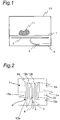
- Fig. 1 is a schematic cross-sectional view of a microwave processing device according to a first embodiment of the present invention.
- the microwave processing device is provided with an object table 1, a periodic structure body 2, an oscillator 3, and a transmitting part 4.
- the object table 1 is to place an object 11 to be heated thereon.
- the periodic structure body 2 is disposed adjacent to the object table 1.
- the oscillator 3 generates microwave power.
- the transmitting part 4 connects the periodic structure body 2 and the oscillator 3 with each other.
- the oscillator 3 for generating microwave power includes a magnetron and/or semiconductors, for example, and the microwave power generated by the oscillator 3 is transmitted to the periodic structure body 2 via the transmitting part 4.
- the periodic structure body 2 is a structure in which substantially the same slits, structures or the like are arrayed at regular intervals to concentrate microwaves, which has been transmitted by the transmitting part 4, in a near space.
- the object 11 to be heated is placed on the object table 1 adjacent to the periodic structure body 2 and will be strongly heated by the microwaves concentrated by the periodic structure body 2, thereby making it possible to brown a surface of the object 11 to be heated.
- the above-described components of the microwave processing device such as the object table 1, the periodic structure body 2 and the like are disposed within a heating chamber 10 of the microwave processing device, but they need not to be always disposed within the heating chamber 10 as long as the microwave processing device has a construction that causes no risk of radio-waves leakage, electric shock or the like.
- Fig. 2 is a bottom plan view of the periodic structure body 2 of the microwave processing device according to the first embodiment.
- the periodic structure body 2 is formed by a pair of thin metallic plates 2a, 2b having a slit formed therein so as to periodically make U-turns.
- the pair of metallic plates 2a, 2b are integrally formed with each other, and the metallic plate 2a occupies an upper half of the periodic structure body 2 shown in Fig. 2 and the metallic plate 2b occupies a lower half of the periodic structure body 2.
- the slit, which periodically makes U-turns in the periodic structure body 2 forms a surface-wave transmission line 9.
- the metallic plates 2a, 2b have a pair of comb-shaped portions 13a, 13b facing each other, respectively.
- the comb-shaped portion 13a of the metallic plate 2a is made up of three metallic plates extending downward in Fig. 2
- the comb-shaped portion 13b of the metallic plate 2b is made up of two metallic plates extending upward in Fig. 2 .
- the surface-wave transmission line 9 formed as a space between the comb-shaped portion 13a and the comb-shaped portion 13b is an interdigital line.
- ending terminals 9a of the surface-wave transmission line 9 are short-circuited, they are not limited to such a case and may be opened.
- Fig. 3 is an enlarged cross-sectional view of the microwave processing device according to the first embodiment.
- the transmitting part 4 is a coaxial cable having a central conductor 6 and a casing 12 to cover the central conductor 6.
- a matching circuit (a matching part) 5 is provided between the central conductor 6 of the transmitting part 4 and the comb-shaped portion 13a of the metallic plate 2a. That is, the central conductor 6 of the transmitting part 4 is connected to the comb-shaped portion 13a of the metallic plate 2a via the matching circuit 5.
- the casing 12 of the transmitting part 4 is connected to a portion of the metallic plate 2b that faces the comb-shaped portion 13a connected to the matching circuit 5 (see Fig. 2 ).
- microwave power is supplied from the transmitting part 4 to the periodic structure body 2, thereby creating an electric field in the surface-wave transmission line 9.
- the surface-wave transmission line 9 acts as a slow-wave circuit by appropriately setting a length, width, interval, or the like of the slit.
- microwaves supplied to the surface-wave transmission line 9 propagate as surface waves having microwave power that reduces in an exponential fashion in a direction perpendicular to a plane including the surface-wave transmission line 9.
- an impedance (for example, 50 ⁇ ) of the transmitting part 4 is smaller than an impedance (for example, 150 ⁇ ) of the periodic structure body 2, and the former is not equal to the latter. Accordingly, if the transmitting part 4 is directly connected to the periodic structure body 2 without the matching circuit 5, large reflection of microwaves may occur at a connecting portion between the transmitting part 4 and the periodic structure body 2 due to their impedance mismatching. The microwave reflection may cause not only a reduction in transmission efficiency of microwave power but also failure of the oscillator 3 or the transmitting part 4. The microwave reflection may also cause emission of microwaves into the heating chamber 10.
- the microwave processing device is provided with the matching circuit 5 at the connecting portion between the periodic structure body 2 and the transmitting part 4, i.e., at the impedance mismatching part.
- the impedance of the matching circuit 5 is set to a value (for example, 100 ⁇ ) between the impedance of the periodic structure body 2 and the impedance of the transmitting part 4.
- the use of the matching circuit 5 to achieve the impedance matching can suppress generation of reflection waves 14 of the microwaves (see Fig. 3 ) or the emission of the microwaves, thus making it possible to enhance the transmission efficiency of microwave power. That is, the microwave power can be efficiently transmitted from the transmitting part 4 to the periodic structure body 2.
- a temperature rise or failure of the oscillator 3 or the transmitting part 4 can be inhibited by suppressing the generation of the reflection waves 14 of the microwaves or the emission of the microwaves, thus making it possible to reduce a size of a cooling structure for the oscillator 3 or the transmitting part 4 and enhance reliability of the microwave processing device.
- the matching circuit 5 is formed by a metallic plate.
- This matching circuit 5 forms a microstrip line in which the periodic structure body 2 (at least a portion of the periodic structure body 2) connected to the casing 12 of the transmitting part 4 acts as a ground surface.
- a dielectric body in the microstrip line is air existing between the periodic structure body 2 and the matching circuit 5.
- the impedance of the matching circuit 5 is defined by a width of the metallic plate forming the matching circuit 5, a distance between the periodic structure body 2 acting as the ground surface and the matching circuit 5, a material of the dielectric body, and the like.
- setting the impedance of the matching circuit 5 to the value between the impedance of the transmitting part 4 and the impedance of the periodic structure body 2 can make a stepwise impedance change between the periodic structure body 2 and the transmitting part 4, thereby making it possible to suppress the generation of the reflection waves 14 of the microwaves or the emission of the microwaves.
- the impedance of the matching circuit 5 is set to an average value of the impedance of the transmitting part 4 and the impedance of the periodic structure body 2, the generation of the reflection waves 14 of the microwaves or the emission of the microwaves can be further suppressed.
- the present invention is not limited to such a case and the impedance of the matching circuit 5 may be set to a value between the impedance of the transmitting part 4 and the impedance of the periodic structure body 2.
- the impedance from the transmitting part 4 to the periodic structure body 2 may be smoothed by changing the width of the metallic plate or the distance between the metallic plate and the ground surface in the matching circuit 5 to become continuous, for example, thereby making it possible to maximally suppress the generation of the reflection waves 14 of the microwaves or the emission of the microwaves.
- the matching circuit 5 and the transmitting part 4 are placed in a space below the periodic structure body 2, the space being not used in cooking the object 11 to be heated. That is, the periodic structure body 2 is placed with respect to the object table 1 on a side (lower side in Fig. 3 ) opposite to a side where the object 11 to be heated is placed, while the matching circuit 5 and the transmitting part 4 are placed with respect to the periodic structure body 2 on a side (lower side in Fig. 3 ) opposite to a side where the object 11 to be heated and the object table 1 are placed.
- This configuration can effectively make use of the void space below the object table 1 and reduce the size of the microwave processing device.
- the microwave processing device is provided with a periodic structure body 2 having a surface-wave transmission line 9 through which surface waves produced by microwaves are transmitted, an oscillator 3 for generating microwave power, and a transmitting part 4 for transmitting the microwave power generated by the oscillator 3 to the periodic structure body 2.
- a matching part 5 is provided at a connecting portion between the periodic structure body 2 and the transmitting part 4, and the impedance of the matching part 5 is set to a value between the impedance of the periodic structure body 2 and the impedance of the transmitting part 4.
- the presence of the matching circuit 5 at the connecting portion between the periodic structure body 2 and the transmitting part 4 can achieve impedance matching at the connecting portion where impedance mismatching may occur, thereby making it possible to suppress the reflection waves 14 of the microwaves generated at the connecting portion and to more efficiently transmit the microwave power from the transmitting part 4 to the periodic structure body 2. Accordingly, not only can the object 11 be efficiently browned by the surface waves of the microwaves, but the size of the microwave processing device can be also reduced.
- Fig. 4 is a bottom plan view of a matching circuit 15 of a microwave processing device according to a first variation of the first embodiment.
- Fig. 5 is a cross-sectional view of the matching circuit 15 of the microwave processing device according to the first variation.
- the first variation shown in Fig. 4 and Fig. 5 differs from the first embodiment shown in Fig. 1 to Fig. 3 only in shape of matching circuit, and the other configurations of the microwave processing device are the same.
- the matching circuit 15 formed by a metallic plate has a tab 17 of a different width formed at an intermediate portion in a longitudinal direction thereof (a horizontal direction in Fig. 4 and Fig. 5 ).
- the tab 17 protrudes in a width direction at the intermediate portion of the matching circuit 15 to form an impedance-changing portion (that is, the tab 17) in the longitudinal direction of the matching circuit 15.
- reflection waves 18 of microwaves are created at the impedance-changing portion formed by the tab 17 at the intermediate portion of the matching circuit 15.
- a position and a shape of the tab 17 are regulated so that the reflection waves 18 of the microwaves created by the tab 17 may have an opposite phase to that of the reflection waves 14 of the microwaves created at the connecting portion between the periodic structure body 2 and the transmitting part 4.
- the reflection waves 14 of the microwaves created at the connecting portion between the periodic structure body 2 and the transmitting part 4 are at least partially cancelled by the reflection waves 18, thereby making it possible to suppress the generation of the reflection waves 14 of the microwaves or the emission of the microwaves and to more efficiently transmit the microwave power from the transmitting part 4 to the periodic structure body 2.
- Fig. 6 is a cross-sectional view of a matching circuit 25 of a microwave processing device according to a second variation of the first embodiment.
- a microstrip line in which the periodic structure body 2 (at least a portion thereof) acts as a ground surface, is provided with a dielectric body 28 different from air at a location between the matching circuit 25 and the periodic structure body 2.
- another dielectric body 28a having a different dielectric constant is provided at an intermediate portion of the dielectric body 28 in a longitudinal direction thereof.
- the dielectric body 28a has an impedance different from that of the other portions of the dielectric body 28. That is, the dielectric body 28a forms an impedance-changing portion in the matching circuit 25.
- reflection waves of the microwaves transmitted from the transmitting part 4 are created.
- materials, positions, shapes and the like of the dielectric bodies 28, 28a are regulated so that the reflection waves of the microwaves created by the impedance-changing portion may have a opposite phase to that of the reflection waves of microwaves created at the connecting portion between the periodic structure body 2 and the transmitting part 4.
- the reflection waves of the microwaves created at the connecting portion between the periodic structure body 2 and the transmitting part 4 are at least partially cancelled, thereby making it possible to suppress the generation of the reflection waves of the microwaves or the emission of the microwaves and to more efficiently transmit the microwave power from the transmitting part 4 to the periodic structure body 2.
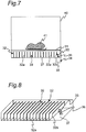
- a microwave processing device according to a second embodiment of the present invention is explained hereinafter with reference to Fig. 7 and Fig. 8 .
- the second embodiment differs from the first embodiment mainly in configuration of periodic structure body forming surface-wave transmission line.
- a periodic structure body 32 of the microwave processing device is made up of a plurality of metallic plates 32a, 32b aligned parallel to one another at regular intervals within a heating chamber 40.
- the plurality of metallic plates 32a are supported from below by a supporting body 37 and only one metallic plate 32b is spaced from the supporting body 37.
- the metallic plate 32b spaced from the supporting body 37 is provided with a matching circuit 35.
- the matching circuit 35 is connected to a central conductor 36 of a transmitting part 34.
- a casing 38 of the transmitting part 34 is connected to the supporting body 37.
- microwave power is transmitted from the transmitting part 34 to the periodic structure body 32 via the matching circuit 35 to create an electric field in a surface-wave transmission line 39 formed between the metallic plates 32a, 32b of the periodic structure body 32.
- surface waves can be produced by microwaves. The surface waves act to heat an object 41 to be heated placed on an object table 31 so as to brown it.
- the impedance of the matching circuit 35 is set to a value between the impedance of the periodic structure body 32 (in particular, the metallic plate 32b) and the impedance of the transmitting part 34.
- the use of the matching circuit 35 at a connecting portion between the periodic structure body 32 and the transmitting part 34 can achieve impedance matching at the connecting portion where impedance mismatching may occur, thereby making it possible to suppress reflection waves of microwaves that may be created at the connecting portion and to more efficiently transmit the microwave power from the transmitting part 34 to the periodic structure body 32. Accordingly, not only can the object 41 be efficiently browned by the surface waves of the microwaves, but the size of the microwave processing device can be also reduced.
- the present invention is not limited to the configurations referred to above, but is practicable in various configurations.
- the metallic plate 2a and the metallic plate 2b have been described as being integrally formed with each other in the periodic structure body 2, but not limited to such a case, the metallic plate 2a and the metallic plate 2b may be formed separately, for example.
- the transmitting part 4 has been described as being a coaxial cable, but not limited to such a case, the transmitting part 4 may be a microstrip line or a strip transmission line, for example.
- the tab 17 has been described as an increase in width at the intermediate portion of the matching circuit 5 to form the impedance-changing portion, but the present invention is not limited to such a case.
- the impedance-changing portion may be provided, for example, by reducing the width of the matching circuit 5 or by changing the thickness of the matching circuit 5, or by using any other method to change the shape of the matching circuit 5.
- the components of the microwave processing device have been described as being disposed within the heating chamber 10, but the present invention is not limited to such a case.
- the components of the microwave processing device may be disposed in an open space instead of within the heating chamber 10 as long as the microwave processing device may have a construction that causes no risk of radio-waves leakage, electric shock or the like.
- the microwave processing device has a surface-wave transmission line formed by a periodic structure body to transmit surface waves produced by microwaves to efficiently transmit microwave power to the periodic structure body. Accordingly, the microwave processing device according to the present invention is applicable to a heating device as represented by a microwave oven that makes use of dielectric heating, a garbage disposer, a stove, a hot plate or the like.
Landscapes
- Physics & Mathematics (AREA)
- Electromagnetism (AREA)
- Engineering & Computer Science (AREA)
- Power Engineering (AREA)
- Constitution Of High-Frequency Heating (AREA)
- Plasma Technology (AREA)
- Waveguide Aerials (AREA)
Description
- The present invention relates to a microwave processing device having a periodic structure body which forms a surface-wave transmission line to transmit surface waves of microwaves.
- A conventional microwave processing device of this kind is provided with a coaxial cable and a periodic structure body. The coaxial cable supplies microwave energy therethrough, and the periodic structure body is supplied with the microwave energy from the coaxial cable and has an interdigital tape line formed therein (see, for example, Patent Document 1). The microwave processing device of
Patent Document 1 has a resonant hole defined in an end of the interdigital tape line. In this configuration, an object to be heated is uniformly heated by microwave heating from the resonant hole, while browning the object using microwaves produced in the interdigital tape line. - In another microwave processing device, microwaves are emitted and transmitted through an interdigital tape line formed by a periodic structure body (see, for example, Patent Document 2). Even a thick object to be heated is efficiently microwave-heated by emitting and transmitting the microwaves through the interdigital tape line.
-
GB 2 081 559claim 1. -
- Patent Document 1: Japanese Laid-Open Patent Publication No.
S61-237393 - Patent Document 2: Japanese Patent Publication No.
H04-61476 - In the above-described conventional configurations, however, when microwave power is transmitted from a transmitting part such as a coaxial cable to the periodic structure body having the surface-wave transmission line such as the interdigital tape line, more efficient transmission of the microwave power to the periodic structure body is required.
- The present invention has been developed to solve the above-described conventional problem and is intended to provide a microwave processing device capable of efficiently transmitting microwave power to a periodic structure body having a surface-wave transmission line.
- In solving the above-described conventional problem, a microwave processing device includes: a periodic structure body which forms a surface-wave transmission line to transmit surface waves of microwaves; an oscillator which generates microwave power; and a transmitting part which transmits the microwave power generated by the oscillator to the periodic structure body, wherein a matching part is provided at a connecting portion between the periodic structure body and the transmitting part, and an impedance of the matching part is set to a value between an impedance of the periodic structure body and an impedance of the transmitting part.
- The microwave processing device of the present invention can efficiently transmit microwave power to a periodic structure body having a surface-wave transmission line.
- These aspects and features of the present invention will become apparent from the following description of preferred embodiments thereof with reference to the accompanying drawings.
-
Fig. 1 is a schematic cross-sectional view of a microwave processing device according to a first embodiment of the present invention. -
Fig. 2 is a bottom plan view of a periodic structure body of the microwave processing device according to the first embodiment. -
Fig. 3 is a cross-sectional view of the microwave processing device according to the first embodiment. -
Fig. 4 is a bottom plan view of a matching circuit of a microwave processing device according to a first variation of the first embodiment. -
Fig. 5 is a cross-sectional view of the matching circuit of the microwave processing device according to the first variation of the first embodiment. -
Fig. 6 is a cross-sectional view of a matching circuit of a microwave processing device according to a second variation of the first embodiment. -
Fig. 7 is a cross-sectionai view of a microwave processing device according to a second embodiment of the present invention. -
Fig. 8 is a perspective view of a periodic structure body of the microwave processing device according to the second embodiment. - A first invention is a microwave processing device including: a periodic structure body which forms a surface-wave transmission line to transmit surface waves of microwaves; an oscillator which generates microwave power; and a transmitting part which transmits the microwave power generated by the oscillator to the periodic structure body, wherein a matching part is provided at a connecting portion between the periodic structure body and the transmitting part, and an impedance of the matching part is set to a value between an impedance of the periodic structure body and an impedance of the transmitting part. This configuration allows the matching part to achieve impedance matching between the transmitting part and the periodic structure body to reduce reflection of microwaves that may occur at the connecting portion between the transmitting part and the periodic structure body, thus making it possible to efficiently transmit the microwave power from the transmitting part to the periodic structure body.
- A second invention is a microwave processing device of the first invention, wherein the matching part forms a microstrip line in which at least a portion of the periodic structure body acts as a ground surface. This configuration can further simplify and downsize the matching part.
- A third invention is a microwave processing device of the first invention, wherein the matching part has an impedance-changing portion that is positioned such that reflection waves of microwaves created at the impedance-changing portion at least partially cancel reflection waves of microwaves created at the connecting portion between the periodic structure body and the matching part. This configuration at least partially cancels the reflection of the microwaves created at the connecting portion between the transmitting part and the periodic structure body, thereby transmitting the microwaves efficiently from the transmitting part to the periodic structure body.
- A fourth invention is a microwave processing device of the third invention, wherein changing of a shape of the matching part forms the impedance-changing portion of the matching part. Thus, the microwaves can be transmitted efficiently from the transmitting part to the periodic structure body.
- A fifth invention is a microwave processing device of the third invention, wherein the matching part forms a microstrip line having a dielectric body in which at least a portion of the periodic structure body acts as a ground surface, and wherein the dielectric body of the microstrip line has a dielectric-constant changing portion, which forms the impedance-changing portion of the matching part. Thus, the microwaves can be transmitted efficiently from the transmitting part to the periodic structure body.
- A sixth invention is a microwave processing device of the first invention, wherein the periodic structure body comprises a first metallic plate having a first comb-shaped portion and a second metallic plate having a second comb-shaped portion positioned to face the first comb-shaped portion, wherein the surface-wave transmission line is an interdigital line between the first and second comb-shaped portions, wherein the transmitting part comprises a coaxial cable which has a central conductor and a casing to cover the central conductor, and wherein the central conductor of the coaxial cable is connected to the first comb-shaped portion of the periodic structure via the matching part, and the casing of the coaxial cable is connected to the second metallic plate of the periodic structure body. This configuration can reduce a thickness of the periodic structure body, thereby reducing the size of the microwave processing device.
- A seventh invention is a microwave processing device of the first invention, wherein the periodic structure body comprises a plurality of metallic plates aligned parallel to one another at regular intervals, and one of the plurality of metallic plates is spaced from a supporting body that supports other metallic plates, wherein the transmitting part comprises a coaxial cable which has a central conductor and a casing to cover the central conductor, and wherein the central conductor is connected via the matching part to the metallic plate spaced from the supporting body, and the casing is connected to the supporting body. Thus, the microwaves can be transmitted efficiently from the transmitting part to the periodic structure body.
- A eighth invention is a microwave processing device of any one the first invention to the seventh invention, further comprising an object table which is disposed adjacent to the surface-wave transmission line to place an object to be heated thereon, wherein the periodic structure body is disposed with respect to the object table on a side opposite to a side where the object to be heated is placed, and wherein at least one of the matching part and the transmitting part is disposed with respect to the periodic structure body on a side opposite to a side where the object to be heated and the object table are placed. This configuration can make efficient use of a space that is not used for cooking, thus making it possible to reduce the size of the microwave processing device.
- First and second embodiments of the present invention are described hereinafter with reference to the drawings, but the present invention is not limited by the first and second embodiments.
-
Fig. 1 is a schematic cross-sectional view of a microwave processing device according to a first embodiment of the present invention. - As shown in
Fig. 1 , the microwave processing device is provided with an object table 1, aperiodic structure body 2, anoscillator 3, and a transmittingpart 4. The object table 1 is to place anobject 11 to be heated thereon. Theperiodic structure body 2 is disposed adjacent to the object table 1. Theoscillator 3 generates microwave power. The transmittingpart 4 connects theperiodic structure body 2 and theoscillator 3 with each other. Theoscillator 3 for generating microwave power includes a magnetron and/or semiconductors, for example, and the microwave power generated by theoscillator 3 is transmitted to theperiodic structure body 2 via the transmittingpart 4. Theperiodic structure body 2 is a structure in which substantially the same slits, structures or the like are arrayed at regular intervals to concentrate microwaves, which has been transmitted by the transmittingpart 4, in a near space. - The
object 11 to be heated is placed on the object table 1 adjacent to theperiodic structure body 2 and will be strongly heated by the microwaves concentrated by theperiodic structure body 2, thereby making it possible to brown a surface of theobject 11 to be heated. - The above-described components of the microwave processing device such as the object table 1, the
periodic structure body 2 and the like are disposed within aheating chamber 10 of the microwave processing device, but they need not to be always disposed within theheating chamber 10 as long as the microwave processing device has a construction that causes no risk of radio-waves leakage, electric shock or the like. -
Fig. 2 is a bottom plan view of theperiodic structure body 2 of the microwave processing device according to the first embodiment. - As shown in
Fig. 2 , theperiodic structure body 2 is formed by a pair of thinmetallic plates metallic plates metallic plate 2a occupies an upper half of theperiodic structure body 2 shown inFig. 2 and themetallic plate 2b occupies a lower half of theperiodic structure body 2. The slit, which periodically makes U-turns in theperiodic structure body 2, forms a surface-wave transmission line 9. As shown inFig. 2 , themetallic plates portions portion 13a of themetallic plate 2a is made up of three metallic plates extending downward inFig. 2 , and the comb-shapedportion 13b of themetallic plate 2b is made up of two metallic plates extending upward inFig. 2 . The surface-wave transmission line 9 formed as a space between the comb-shapedportion 13a and the comb-shapedportion 13b is an interdigital line. Although in the firstembodiment ending terminals 9a of the surface-wave transmission line 9 are short-circuited, they are not limited to such a case and may be opened. -
Fig. 3 is an enlarged cross-sectional view of the microwave processing device according to the first embodiment. - As shown in
Fig. 3 , the transmittingpart 4 according to the first embodiment is a coaxial cable having acentral conductor 6 and acasing 12 to cover thecentral conductor 6. As shown inFig. 2 andFig. 3 , a matching circuit (a matching part) 5 is provided between thecentral conductor 6 of the transmittingpart 4 and the comb-shapedportion 13a of themetallic plate 2a. That is, thecentral conductor 6 of the transmittingpart 4 is connected to the comb-shapedportion 13a of themetallic plate 2a via thematching circuit 5. Thecasing 12 of the transmittingpart 4 is connected to a portion of themetallic plate 2b that faces the comb-shapedportion 13a connected to the matching circuit 5 (seeFig. 2 ). In such a connecting relation between theperiodic structure body 2 and the transmittingpart 4, microwave power is supplied from the transmittingpart 4 to theperiodic structure body 2, thereby creating an electric field in the surface-wave transmission line 9. The surface-wave transmission line 9 acts as a slow-wave circuit by appropriately setting a length, width, interval, or the like of the slit. Thus, microwaves supplied to the surface-wave transmission line 9 propagate as surface waves having microwave power that reduces in an exponential fashion in a direction perpendicular to a plane including the surface-wave transmission line 9. - In most cases, an impedance (for example, 50 Ω) of the transmitting
part 4 is smaller than an impedance (for example, 150 Ω) of theperiodic structure body 2, and the former is not equal to the latter. Accordingly, if the transmittingpart 4 is directly connected to theperiodic structure body 2 without thematching circuit 5, large reflection of microwaves may occur at a connecting portion between the transmittingpart 4 and theperiodic structure body 2 due to their impedance mismatching. The microwave reflection may cause not only a reduction in transmission efficiency of microwave power but also failure of theoscillator 3 or the transmittingpart 4. The microwave reflection may also cause emission of microwaves into theheating chamber 10. - For this reason, the microwave processing device according to the first embodiment is provided with the
matching circuit 5 at the connecting portion between theperiodic structure body 2 and the transmittingpart 4, i.e., at the impedance mismatching part. Further, the impedance of thematching circuit 5 is set to a value (for example, 100 Ω) between the impedance of theperiodic structure body 2 and the impedance of the transmittingpart 4. The use of thematching circuit 5 to achieve the impedance matching can suppress generation of reflection waves 14 of the microwaves (seeFig. 3 ) or the emission of the microwaves, thus making it possible to enhance the transmission efficiency of microwave power. That is, the microwave power can be efficiently transmitted from the transmittingpart 4 to theperiodic structure body 2. - Also, a temperature rise or failure of the
oscillator 3 or the transmittingpart 4 can be inhibited by suppressing the generation of the reflection waves 14 of the microwaves or the emission of the microwaves, thus making it possible to reduce a size of a cooling structure for theoscillator 3 or the transmittingpart 4 and enhance reliability of the microwave processing device. - The
matching circuit 5 according to the first embodiment is formed by a metallic plate. Thismatching circuit 5 forms a microstrip line in which the periodic structure body 2 (at least a portion of the periodic structure body 2) connected to thecasing 12 of the transmittingpart 4 acts as a ground surface. A dielectric body in the microstrip line is air existing between theperiodic structure body 2 and thematching circuit 5. The impedance of thematching circuit 5 is defined by a width of the metallic plate forming thematching circuit 5, a distance between theperiodic structure body 2 acting as the ground surface and thematching circuit 5, a material of the dielectric body, and the like. As described above, in the first embodiment, setting the impedance of thematching circuit 5 to the value between the impedance of the transmittingpart 4 and the impedance of theperiodic structure body 2 can make a stepwise impedance change between theperiodic structure body 2 and the transmittingpart 4, thereby making it possible to suppress the generation of the reflection waves 14 of the microwaves or the emission of the microwaves. - If the impedance of the
matching circuit 5 is set to an average value of the impedance of the transmittingpart 4 and the impedance of theperiodic structure body 2, the generation of the reflection waves 14 of the microwaves or the emission of the microwaves can be further suppressed. However, the present invention is not limited to such a case and the impedance of thematching circuit 5 may be set to a value between the impedance of the transmittingpart 4 and the impedance of theperiodic structure body 2. Alternatively, the impedance from the transmittingpart 4 to theperiodic structure body 2 may be smoothed by changing the width of the metallic plate or the distance between the metallic plate and the ground surface in thematching circuit 5 to become continuous, for example, thereby making it possible to maximally suppress the generation of the reflection waves 14 of the microwaves or the emission of the microwaves. - Also, in the first embodiment, the
matching circuit 5 and the transmittingpart 4 are placed in a space below theperiodic structure body 2, the space being not used in cooking theobject 11 to be heated. That is, theperiodic structure body 2 is placed with respect to the object table 1 on a side (lower side inFig. 3 ) opposite to a side where theobject 11 to be heated is placed, while thematching circuit 5 and the transmittingpart 4 are placed with respect to theperiodic structure body 2 on a side (lower side inFig. 3 ) opposite to a side where theobject 11 to be heated and the object table 1 are placed. This configuration can effectively make use of the void space below the object table 1 and reduce the size of the microwave processing device. - As just described, the microwave processing device according to the first embodiment is provided with a
periodic structure body 2 having a surface-wave transmission line 9 through which surface waves produced by microwaves are transmitted, anoscillator 3 for generating microwave power, and a transmittingpart 4 for transmitting the microwave power generated by theoscillator 3 to theperiodic structure body 2. Amatching part 5 is provided at a connecting portion between theperiodic structure body 2 and the transmittingpart 4, and the impedance of thematching part 5 is set to a value between the impedance of theperiodic structure body 2 and the impedance of the transmittingpart 4. The presence of thematching circuit 5 at the connecting portion between theperiodic structure body 2 and the transmittingpart 4 can achieve impedance matching at the connecting portion where impedance mismatching may occur, thereby making it possible to suppress the reflection waves 14 of the microwaves generated at the connecting portion and to more efficiently transmit the microwave power from the transmittingpart 4 to theperiodic structure body 2. Accordingly, not only can theobject 11 be efficiently browned by the surface waves of the microwaves, but the size of the microwave processing device can be also reduced. -
Fig. 4 is a bottom plan view of amatching circuit 15 of a microwave processing device according to a first variation of the first embodiment.Fig. 5 is a cross-sectional view of the matchingcircuit 15 of the microwave processing device according to the first variation. The first variation shown inFig. 4 andFig. 5 differs from the first embodiment shown inFig. 1 to Fig. 3 only in shape of matching circuit, and the other configurations of the microwave processing device are the same. - In the first variation, as shown in
Fig. 4 andFig. 5 , the matchingcircuit 15 formed by a metallic plate has atab 17 of a different width formed at an intermediate portion in a longitudinal direction thereof (a horizontal direction inFig. 4 andFig. 5 ). Thetab 17 protrudes in a width direction at the intermediate portion of the matchingcircuit 15 to form an impedance-changing portion (that is, the tab 17) in the longitudinal direction of the matchingcircuit 15. - As shown in
Fig. 5 , reflection waves 18 of microwaves are created at the impedance-changing portion formed by thetab 17 at the intermediate portion of the matchingcircuit 15. In the first variation, a position and a shape of thetab 17 are regulated so that the reflection waves 18 of the microwaves created by thetab 17 may have an opposite phase to that of the reflection waves 14 of the microwaves created at the connecting portion between theperiodic structure body 2 and the transmittingpart 4. Thus, the reflection waves 14 of the microwaves created at the connecting portion between theperiodic structure body 2 and the transmittingpart 4 are at least partially cancelled by the reflection waves 18, thereby making it possible to suppress the generation of the reflection waves 14 of the microwaves or the emission of the microwaves and to more efficiently transmit the microwave power from the transmittingpart 4 to theperiodic structure body 2. -
Fig. 6 is a cross-sectional view of amatching circuit 25 of a microwave processing device according to a second variation of the first embodiment. In the second variation shown inFig. 6 , a microstrip line, in which the periodic structure body 2 (at least a portion thereof) acts as a ground surface, is provided with adielectric body 28 different from air at a location between the matchingcircuit 25 and theperiodic structure body 2. Also, in the second variation, anotherdielectric body 28a having a different dielectric constant is provided at an intermediate portion of thedielectric body 28 in a longitudinal direction thereof. Thedielectric body 28a has an impedance different from that of the other portions of thedielectric body 28. That is, thedielectric body 28a forms an impedance-changing portion in thematching circuit 25. - In the impedance-changing portion formed by the
dielectric body 28a, reflection waves of the microwaves transmitted from the transmittingpart 4 are created. In the second variation, as in the first variation, materials, positions, shapes and the like of thedielectric bodies periodic structure body 2 and the transmittingpart 4. Thus, the reflection waves of the microwaves created at the connecting portion between theperiodic structure body 2 and the transmittingpart 4 are at least partially cancelled, thereby making it possible to suppress the generation of the reflection waves of the microwaves or the emission of the microwaves and to more efficiently transmit the microwave power from the transmittingpart 4 to theperiodic structure body 2. - A microwave processing device according to a second embodiment of the present invention is explained hereinafter with reference to
Fig. 7 and Fig. 8 . The second embodiment differs from the first embodiment mainly in configuration of periodic structure body forming surface-wave transmission line. - A
periodic structure body 32 of the microwave processing device according to the second embodiment is made up of a plurality ofmetallic plates heating chamber 40. The plurality ofmetallic plates 32a are supported from below by a supportingbody 37 and only onemetallic plate 32b is spaced from the supportingbody 37. Themetallic plate 32b spaced from the supportingbody 37 is provided with amatching circuit 35. The matchingcircuit 35 is connected to acentral conductor 36 of a transmittingpart 34. Acasing 38 of the transmittingpart 34 is connected to the supportingbody 37. - In such a configuration also, microwave power is transmitted from the transmitting
part 34 to theperiodic structure body 32 via thematching circuit 35 to create an electric field in a surface-wave transmission line 39 formed between themetallic plates periodic structure body 32. Accordingly, in the surface-wave transmission line 39, surface waves can be produced by microwaves. The surface waves act to heat anobject 41 to be heated placed on an object table 31 so as to brown it. - In the second embodiment also, as in the first embodiment, the impedance of the matching
circuit 35 is set to a value between the impedance of the periodic structure body 32 (in particular, themetallic plate 32b) and the impedance of the transmittingpart 34. The use of the matchingcircuit 35 at a connecting portion between theperiodic structure body 32 and the transmittingpart 34 can achieve impedance matching at the connecting portion where impedance mismatching may occur, thereby making it possible to suppress reflection waves of microwaves that may be created at the connecting portion and to more efficiently transmit the microwave power from the transmittingpart 34 to theperiodic structure body 32. Accordingly, not only can theobject 41 be efficiently browned by the surface waves of the microwaves, but the size of the microwave processing device can be also reduced. - It is to be noted that the present invention is not limited to the configurations referred to above, but is practicable in various configurations. For example, in the first embodiment, the
metallic plate 2a and themetallic plate 2b have been described as being integrally formed with each other in theperiodic structure body 2, but not limited to such a case, themetallic plate 2a and themetallic plate 2b may be formed separately, for example. - Also, in the first and second embodiments the transmitting
part 4 has been described as being a coaxial cable, but not limited to such a case, the transmittingpart 4 may be a microstrip line or a strip transmission line, for example. - Further, in the first variation of the first embodiment the
tab 17 has been described as an increase in width at the intermediate portion of thematching circuit 5 to form the impedance-changing portion, but the present invention is not limited to such a case. The impedance-changing portion may be provided, for example, by reducing the width of thematching circuit 5 or by changing the thickness of thematching circuit 5, or by using any other method to change the shape of thematching circuit 5. - Also, in the first and second embodiments the components of the microwave processing device have been described as being disposed within the
heating chamber 10, but the present invention is not limited to such a case. The components of the microwave processing device may be disposed in an open space instead of within theheating chamber 10 as long as the microwave processing device may have a construction that causes no risk of radio-waves leakage, electric shock or the like. - Any combination of the various embodiments referred to above can produce respective effects.
- As described above, the microwave processing device according to the present invention has a surface-wave transmission line formed by a periodic structure body to transmit surface waves produced by microwaves to efficiently transmit microwave power to the periodic structure body. Accordingly, the microwave processing device according to the present invention is applicable to a heating device as represented by a microwave oven that makes use of dielectric heating, a garbage disposer, a stove, a hot plate or the like.
- Although the present invention has been fully described by way of preferred embodiments with reference to the accompanying drawings, it is to be noted here that various changes and modifications will be apparent to those skilled in the art. Therefore, unless such changes and modifications otherwise depart from the scope of the present invention as set forth in the appended claims, they should be construed as being included therein.
- The contents of a specification, drawings and claims of a Japanese patent application No.
2012-267919 filed December 7, 2012
Claims (6)
- A microwave processing device comprising:a periodic structure body (2) which forms a surface-wave transmission line (9) to transmit surface waves of microwaves;an oscillator (3) which generates microwave power; anda transmitting part (4) which transmits the microwave power generated by the oscillator (3) to the periodic structure body (2), whereina matching part (5, 15, 25) is provided at a connecting portion between the periodic structure body (2) and the transmitting part (4), and an impedance of the matching part (5, 15, 25) is set to a value between an impedance of the periodic structure body (2) and an impedance of the transmitting part (4), whereinthe matching part (5, 15, 25) has an impedance-changing portion that is positioned such that reflection waves (18) of microwaves created at the impedance-changing portion at least partially cancel reflection waves (14) of microwaves created at the connecting portion between the periodic structure body (2) and the matching part (5, 15, 25);wherein changing of a shape of the matching part (5, 15, 25) forms the impedance-changing portion of the matching part (5, 15, 25); andcharacterized in that the matching part (5, 15, 25) is formed by a metallic plate having a tab (17) of a different width in comparison with the width of the rest of the matching part (5, 15, 25) formed at an intermediate portion in a longitudinal direction thereof.
- The microwave processing device according to claim 1, wherein the matching part (5, 15, 25) forms a microstrip line in which at least a portion of the periodic structure body (2) acts as a ground surface.
- The microwave processing device according to claim 1, wherein the matching part (5, 15, 25) forms a microstrip line having a dielectric body (28) in which at least a portion of the periodic structure body (2) acts as a ground surface, and wherein
the dielectric body (28) of the microstrip line has a dielectric-constant changing portion, which forms the impedance-changing portion of the matching part (5, 15, 25). - The microwave processing device according to claim 1, wherein the periodic structure body (2) comprises a first metallic plate (2b) having a first comb-shaped portion (13a) and a second metallic plate (2a) having a second comb-shaped portion (13b) positioned to face the first comb-shaped portion (13a), wherein
the surface-wave transmission line (9) is an interdigital line between the first and second comb-shaped portions (13a, 13b), wherein
the transmitting part (4) comprises a coaxial cable which has a central conductor (6) and a casing (12) to cover the central conductor (6), and wherein
the central conductor (6) of the coaxial cable is connected to the first comb-shaped portion (13a) of the periodic structure (2) via the matching part (5, 15, 25), and the casing (12) of the coaxial cable is connected to the second metallic plate (2b) of the periodic structure body (2). - The microwave processing device according to claim 1, wherein the periodic structure body (2) comprises a plurality of metallic plates (32a, 32b) aligned parallel to one another at regular intervals, and one (32b) of the plurality of metallic plates (32a, 32b) is spaced from a supporting body (37) that supports other metallic plates (32a), wherein
the transmitting part (4) comprises a coaxial cable which has a central conductor (6) and a casing (12) to cover the central conductor (6), and wherein
the central conductor (6) is connected via the matching part (5, 15, 25) to the metallic plate (32b) spaced from the supporting body (37), and the casing (38) is connected to the supporting body (37). - The microwave processing device according to any one of claims 1 to 5, further comprising an object table (1) which is disposed adjacent to the surface-wave transmission line (9) to place an object (11) to be heated thereon, wherein
the periodic structure body (2) is disposed with respect to the object table (1) on a side opposite to a side where the object (11) to be heated is placed, and wherein
at least one of the matching part (5, 15, 25) and the transmitting part (4) is disposed with respect to the periodic structure body (2) on a side opposite to a side where the object (11) to be heated and the object table (1) are placed.
Applications Claiming Priority (2)
| Application Number | Priority Date | Filing Date | Title |
|---|---|---|---|
| JP2012267919 | 2012-12-07 | ||
| PCT/JP2013/007200 WO2014087666A1 (en) | 2012-12-07 | 2013-12-06 | Microwave processing device |
Publications (3)
| Publication Number | Publication Date |
|---|---|
| EP2931007A1 EP2931007A1 (en) | 2015-10-14 |
| EP2931007A4 EP2931007A4 (en) | 2015-12-23 |
| EP2931007B1 true EP2931007B1 (en) | 2019-02-06 |
Family
ID=50883106
Family Applications (1)
| Application Number | Title | Priority Date | Filing Date |
|---|---|---|---|
| EP13860191.9A Active EP2931007B1 (en) | 2012-12-07 | 2013-12-06 | Microwave processing device |
Country Status (5)
| Country | Link |
|---|---|
| US (1) | US9876481B2 (en) |
| EP (1) | EP2931007B1 (en) |
| JP (1) | JP6288461B2 (en) |
| CN (1) | CN104604331B (en) |
| WO (1) | WO2014087666A1 (en) |
Families Citing this family (12)
| Publication number | Priority date | Publication date | Assignee | Title |
|---|---|---|---|---|
| EP3177109A1 (en) * | 2015-12-04 | 2017-06-07 | Electrolux Appliances Aktiebolag | Microwave oven |
| EP3481150B1 (en) * | 2016-06-30 | 2022-02-23 | Panasonic Intellectual Property Management Co., Ltd. | High-frequency heating device |
| CN109076656B (en) * | 2016-08-22 | 2020-12-08 | 松下知识产权经营株式会社 | High frequency heating device |
| JP6715515B2 (en) * | 2016-08-22 | 2020-07-01 | パナソニックIpマネジメント株式会社 | High frequency heating device |
| JP6967708B2 (en) * | 2016-08-22 | 2021-11-17 | パナソニックIpマネジメント株式会社 | High frequency heating device |
| SG10201913381PA (en) * | 2017-05-23 | 2020-03-30 | Microwave Chemical Co Ltd | Treatment apparatus |
| US10161667B1 (en) * | 2017-11-15 | 2018-12-25 | Haier Us Appliance Solutions, Inc. | Refrigerator appliance having a defrost chamber |
| WO2019194098A1 (en) * | 2018-04-06 | 2019-10-10 | パナソニックIpマネジメント株式会社 | High-frequency heating device |
| CN108924984A (en) * | 2018-08-21 | 2018-11-30 | 电子科技大学 | A kind of surface wave heating device for heat foods |
| JP7178556B2 (en) * | 2019-03-27 | 2022-11-28 | パナソニックIpマネジメント株式会社 | High frequency heating device |
| CN114062796B (en) * | 2020-08-04 | 2023-11-14 | 青岛海尔电冰箱有限公司 | Detection device for electromagnetic wave generation system |
| JP2023148648A (en) * | 2022-03-30 | 2023-10-13 | パナソニックIpマネジメント株式会社 | High frequency heating device |
Family Cites Families (15)
| Publication number | Priority date | Publication date | Assignee | Title |
|---|---|---|---|---|
| JPS5112130B2 (en) | 1972-06-08 | 1976-04-16 | ||
| JPS5111242A (en) * | 1974-07-17 | 1976-01-29 | Matsushita Electric Industrial Co Ltd | |
| JPS51128038A (en) * | 1975-04-30 | 1976-11-08 | Matsushita Electric Ind Co Ltd | High-frequency heating apparatus |
| US4121078A (en) | 1975-04-30 | 1978-10-17 | Matsushita Electric Industrial Co., Ltd. | Microwave heating apparatus |
| JPS51148842A (en) * | 1975-06-16 | 1976-12-21 | Matsushita Electric Ind Co Ltd | High frequency hea ting apparatus |
| US4399341A (en) * | 1980-08-06 | 1983-08-16 | Sanyo Electric Co., Ltd. | Microwave heating apparatus |
| JPS57189492A (en) * | 1981-05-19 | 1982-11-20 | Sanyo Electric Co | Microwave heater |
| JPS61237393A (en) * | 1985-04-11 | 1986-10-22 | 松下電器産業株式会社 | High frequency heating device |
| JPS61243692A (en) * | 1985-04-19 | 1986-10-29 | 松下電器産業株式会社 | High frequency heating device |
| JPS61259490A (en) | 1985-05-14 | 1986-11-17 | 松下電器産業株式会社 | High frequency heating device |
| JPS628493A (en) * | 1985-07-02 | 1987-01-16 | 松下電器産業株式会社 | High frequency heating device |
| US4695693A (en) | 1986-10-02 | 1987-09-22 | General Electric Company | Triangular antenna array for microwave oven |
| JPH0461476A (en) | 1990-06-29 | 1992-02-27 | Casio Comput Co Ltd | Picture processor |
| EP2230881B1 (en) * | 2009-03-20 | 2018-11-28 | Whirlpool Corporation | Microwave heating device |
| US10361487B2 (en) * | 2011-07-29 | 2019-07-23 | University Of Saskatchewan | Polymer-based resonator antennas |
-
2013
- 2013-12-06 WO PCT/JP2013/007200 patent/WO2014087666A1/en not_active Ceased
- 2013-12-06 JP JP2014550937A patent/JP6288461B2/en active Active
- 2013-12-06 EP EP13860191.9A patent/EP2931007B1/en active Active
- 2013-12-06 CN CN201380046100.1A patent/CN104604331B/en active Active
- 2013-12-06 US US14/426,034 patent/US9876481B2/en active Active
Non-Patent Citations (1)
| Title |
|---|
| None * |
Also Published As
| Publication number | Publication date |
|---|---|
| JP6288461B2 (en) | 2018-03-07 |
| CN104604331A (en) | 2015-05-06 |
| CN104604331B (en) | 2017-04-05 |
| EP2931007A4 (en) | 2015-12-23 |
| US9876481B2 (en) | 2018-01-23 |
| WO2014087666A1 (en) | 2014-06-12 |
| US20150288342A1 (en) | 2015-10-08 |
| JPWO2014087666A1 (en) | 2017-01-05 |
| EP2931007A1 (en) | 2015-10-14 |
Similar Documents
| Publication | Publication Date | Title |
|---|---|---|
| EP2931007B1 (en) | Microwave processing device | |
| US10356855B2 (en) | Microwave heating apparatus | |
| EP3111724B1 (en) | Microwave oven having a physically adjustable waveguide dynamically displaced by a movement control means | |
| US9179506B2 (en) | Door choke and cooking apparatus including the same | |
| CN103080656B (en) | Cooking equipment | |
| CN106642232A (en) | Microwave oven | |
| CN106545899B (en) | Rectangular waveguide component and microwave oven with same | |
| CN105509109B (en) | Micro-wave oven | |
| EP3384731B1 (en) | Microwave oven | |
| CN103650637A (en) | Microwave heating device | |
| CN106231711B (en) | The antenna module and micro-wave oven of micro-wave oven | |
| CN110056915A (en) | Cooking apparatus | |
| CN105491702B (en) | Antennas and microwave ovens for microwave heating equipment | |
| CN110741731B (en) | Microwave cooking appliance with patch antenna | |
| JP6715515B2 (en) | High frequency heating device | |
| EP3481149A1 (en) | High-frequency heating device | |
| JPH11135251A (en) | microwave | |
| CN221197474U (en) | Cooking utensil | |
| CN117676945A (en) | Microwave heating apparatus | |
| JPS6346551B2 (en) | ||
| JP6861332B2 (en) | High frequency heating device | |
| CN113365380A (en) | Structural member for radiation heating, assembly and heating equipment | |
| CN121310330A (en) | An excitation structure and a microwave oven | |
| CN102384513A (en) | Protective cover of roasting pipe | |
| CN112556294B (en) | Heating device and refrigerator including same |
Legal Events
| Date | Code | Title | Description |
|---|---|---|---|
| PUAI | Public reference made under article 153(3) epc to a published international application that has entered the european phase |
Free format text: ORIGINAL CODE: 0009012 |
|
| 17P | Request for examination filed |
Effective date: 20150609 |
|
| AK | Designated contracting states |
Kind code of ref document: A1 Designated state(s): AL AT BE BG CH CY CZ DE DK EE ES FI FR GB GR HR HU IE IS IT LI LT LU LV MC MK MT NL NO PL PT RO RS SE SI SK SM TR |
|
| AX | Request for extension of the european patent |
Extension state: BA ME |
|
| RA4 | Supplementary search report drawn up and despatched (corrected) |
Effective date: 20151120 |
|
| RIC1 | Information provided on ipc code assigned before grant |
Ipc: H05B 6/74 20060101ALI20151116BHEP Ipc: H05B 6/70 20060101AFI20151116BHEP |
|
| DAX | Request for extension of the european patent (deleted) | ||
| GRAP | Despatch of communication of intention to grant a patent |
Free format text: ORIGINAL CODE: EPIDOSNIGR1 |
|
| STAA | Information on the status of an ep patent application or granted ep patent |
Free format text: STATUS: GRANT OF PATENT IS INTENDED |
|
| INTG | Intention to grant announced |
Effective date: 20180710 |
|
| GRAS | Grant fee paid |
Free format text: ORIGINAL CODE: EPIDOSNIGR3 |
|
| GRAA | (expected) grant |
Free format text: ORIGINAL CODE: 0009210 |
|
| STAA | Information on the status of an ep patent application or granted ep patent |
Free format text: STATUS: THE PATENT HAS BEEN GRANTED |
|
| AK | Designated contracting states |
Kind code of ref document: B1 Designated state(s): AL AT BE BG CH CY CZ DE DK EE ES FI FR GB GR HR HU IE IS IT LI LT LU LV MC MK MT NL NO PL PT RO RS SE SI SK SM TR |
|
| REG | Reference to a national code |
Ref country code: GB Ref legal event code: FG4D |
|
| REG | Reference to a national code |
Ref country code: CH Ref legal event code: EP Ref country code: AT Ref legal event code: REF Ref document number: 1095674 Country of ref document: AT Kind code of ref document: T Effective date: 20190215 |
|
| REG | Reference to a national code |
Ref country code: IE Ref legal event code: FG4D |
|
| REG | Reference to a national code |
Ref country code: DE Ref legal event code: R096 Ref document number: 602013050616 Country of ref document: DE |
|
| REG | Reference to a national code |
Ref country code: NL Ref legal event code: MP Effective date: 20190206 |
|
| REG | Reference to a national code |
Ref country code: LT Ref legal event code: MG4D |
|
| PG25 | Lapsed in a contracting state [announced via postgrant information from national office to epo] |
Ref country code: PT Free format text: LAPSE BECAUSE OF FAILURE TO SUBMIT A TRANSLATION OF THE DESCRIPTION OR TO PAY THE FEE WITHIN THE PRESCRIBED TIME-LIMIT Effective date: 20190606 Ref country code: FI Free format text: LAPSE BECAUSE OF FAILURE TO SUBMIT A TRANSLATION OF THE DESCRIPTION OR TO PAY THE FEE WITHIN THE PRESCRIBED TIME-LIMIT Effective date: 20190206 Ref country code: LT Free format text: LAPSE BECAUSE OF FAILURE TO SUBMIT A TRANSLATION OF THE DESCRIPTION OR TO PAY THE FEE WITHIN THE PRESCRIBED TIME-LIMIT Effective date: 20190206 Ref country code: NL Free format text: LAPSE BECAUSE OF FAILURE TO SUBMIT A TRANSLATION OF THE DESCRIPTION OR TO PAY THE FEE WITHIN THE PRESCRIBED TIME-LIMIT Effective date: 20190206 Ref country code: SE Free format text: LAPSE BECAUSE OF FAILURE TO SUBMIT A TRANSLATION OF THE DESCRIPTION OR TO PAY THE FEE WITHIN THE PRESCRIBED TIME-LIMIT Effective date: 20190206 Ref country code: NO Free format text: LAPSE BECAUSE OF FAILURE TO SUBMIT A TRANSLATION OF THE DESCRIPTION OR TO PAY THE FEE WITHIN THE PRESCRIBED TIME-LIMIT Effective date: 20190506 |
|
| REG | Reference to a national code |
Ref country code: AT Ref legal event code: MK05 Ref document number: 1095674 Country of ref document: AT Kind code of ref document: T Effective date: 20190206 |
|
| PG25 | Lapsed in a contracting state [announced via postgrant information from national office to epo] |
Ref country code: HR Free format text: LAPSE BECAUSE OF FAILURE TO SUBMIT A TRANSLATION OF THE DESCRIPTION OR TO PAY THE FEE WITHIN THE PRESCRIBED TIME-LIMIT Effective date: 20190206 Ref country code: RS Free format text: LAPSE BECAUSE OF FAILURE TO SUBMIT A TRANSLATION OF THE DESCRIPTION OR TO PAY THE FEE WITHIN THE PRESCRIBED TIME-LIMIT Effective date: 20190206 Ref country code: LV Free format text: LAPSE BECAUSE OF FAILURE TO SUBMIT A TRANSLATION OF THE DESCRIPTION OR TO PAY THE FEE WITHIN THE PRESCRIBED TIME-LIMIT Effective date: 20190206 Ref country code: GR Free format text: LAPSE BECAUSE OF FAILURE TO SUBMIT A TRANSLATION OF THE DESCRIPTION OR TO PAY THE FEE WITHIN THE PRESCRIBED TIME-LIMIT Effective date: 20190507 Ref country code: IS Free format text: LAPSE BECAUSE OF FAILURE TO SUBMIT A TRANSLATION OF THE DESCRIPTION OR TO PAY THE FEE WITHIN THE PRESCRIBED TIME-LIMIT Effective date: 20190606 Ref country code: BG Free format text: LAPSE BECAUSE OF FAILURE TO SUBMIT A TRANSLATION OF THE DESCRIPTION OR TO PAY THE FEE WITHIN THE PRESCRIBED TIME-LIMIT Effective date: 20190506 |
|
| PG25 | Lapsed in a contracting state [announced via postgrant information from national office to epo] |
Ref country code: EE Free format text: LAPSE BECAUSE OF FAILURE TO SUBMIT A TRANSLATION OF THE DESCRIPTION OR TO PAY THE FEE WITHIN THE PRESCRIBED TIME-LIMIT Effective date: 20190206 Ref country code: DK Free format text: LAPSE BECAUSE OF FAILURE TO SUBMIT A TRANSLATION OF THE DESCRIPTION OR TO PAY THE FEE WITHIN THE PRESCRIBED TIME-LIMIT Effective date: 20190206 Ref country code: IT Free format text: LAPSE BECAUSE OF FAILURE TO SUBMIT A TRANSLATION OF THE DESCRIPTION OR TO PAY THE FEE WITHIN THE PRESCRIBED TIME-LIMIT Effective date: 20190206 Ref country code: CZ Free format text: LAPSE BECAUSE OF FAILURE TO SUBMIT A TRANSLATION OF THE DESCRIPTION OR TO PAY THE FEE WITHIN THE PRESCRIBED TIME-LIMIT Effective date: 20190206 Ref country code: RO Free format text: LAPSE BECAUSE OF FAILURE TO SUBMIT A TRANSLATION OF THE DESCRIPTION OR TO PAY THE FEE WITHIN THE PRESCRIBED TIME-LIMIT Effective date: 20190206 Ref country code: AL Free format text: LAPSE BECAUSE OF FAILURE TO SUBMIT A TRANSLATION OF THE DESCRIPTION OR TO PAY THE FEE WITHIN THE PRESCRIBED TIME-LIMIT Effective date: 20190206 Ref country code: ES Free format text: LAPSE BECAUSE OF FAILURE TO SUBMIT A TRANSLATION OF THE DESCRIPTION OR TO PAY THE FEE WITHIN THE PRESCRIBED TIME-LIMIT Effective date: 20190206 Ref country code: SK Free format text: LAPSE BECAUSE OF FAILURE TO SUBMIT A TRANSLATION OF THE DESCRIPTION OR TO PAY THE FEE WITHIN THE PRESCRIBED TIME-LIMIT Effective date: 20190206 |
|
| REG | Reference to a national code |
Ref country code: DE Ref legal event code: R097 Ref document number: 602013050616 Country of ref document: DE |
|
| PG25 | Lapsed in a contracting state [announced via postgrant information from national office to epo] |
Ref country code: PL Free format text: LAPSE BECAUSE OF FAILURE TO SUBMIT A TRANSLATION OF THE DESCRIPTION OR TO PAY THE FEE WITHIN THE PRESCRIBED TIME-LIMIT Effective date: 20190206 Ref country code: SM Free format text: LAPSE BECAUSE OF FAILURE TO SUBMIT A TRANSLATION OF THE DESCRIPTION OR TO PAY THE FEE WITHIN THE PRESCRIBED TIME-LIMIT Effective date: 20190206 |
|
| PLBE | No opposition filed within time limit |
Free format text: ORIGINAL CODE: 0009261 |
|
| STAA | Information on the status of an ep patent application or granted ep patent |
Free format text: STATUS: NO OPPOSITION FILED WITHIN TIME LIMIT |
|
| PG25 | Lapsed in a contracting state [announced via postgrant information from national office to epo] |
Ref country code: AT Free format text: LAPSE BECAUSE OF FAILURE TO SUBMIT A TRANSLATION OF THE DESCRIPTION OR TO PAY THE FEE WITHIN THE PRESCRIBED TIME-LIMIT Effective date: 20190206 |
|
| 26N | No opposition filed |
Effective date: 20191107 |
|
| PG25 | Lapsed in a contracting state [announced via postgrant information from national office to epo] |
Ref country code: SI Free format text: LAPSE BECAUSE OF FAILURE TO SUBMIT A TRANSLATION OF THE DESCRIPTION OR TO PAY THE FEE WITHIN THE PRESCRIBED TIME-LIMIT Effective date: 20190206 |
|
| PG25 | Lapsed in a contracting state [announced via postgrant information from national office to epo] |
Ref country code: TR Free format text: LAPSE BECAUSE OF FAILURE TO SUBMIT A TRANSLATION OF THE DESCRIPTION OR TO PAY THE FEE WITHIN THE PRESCRIBED TIME-LIMIT Effective date: 20190206 |
|
| REG | Reference to a national code |
Ref country code: CH Ref legal event code: PL |
|
| REG | Reference to a national code |
Ref country code: BE Ref legal event code: MM Effective date: 20191231 |
|
| PG25 | Lapsed in a contracting state [announced via postgrant information from national office to epo] |
Ref country code: MC Free format text: LAPSE BECAUSE OF FAILURE TO SUBMIT A TRANSLATION OF THE DESCRIPTION OR TO PAY THE FEE WITHIN THE PRESCRIBED TIME-LIMIT Effective date: 20190206 |
|
| PG25 | Lapsed in a contracting state [announced via postgrant information from national office to epo] |
Ref country code: IE Free format text: LAPSE BECAUSE OF NON-PAYMENT OF DUE FEES Effective date: 20191206 Ref country code: FR Free format text: LAPSE BECAUSE OF NON-PAYMENT OF DUE FEES Effective date: 20191231 Ref country code: LU Free format text: LAPSE BECAUSE OF NON-PAYMENT OF DUE FEES Effective date: 20191206 |
|
| PG25 | Lapsed in a contracting state [announced via postgrant information from national office to epo] |
Ref country code: BE Free format text: LAPSE BECAUSE OF NON-PAYMENT OF DUE FEES Effective date: 20191231 Ref country code: LI Free format text: LAPSE BECAUSE OF NON-PAYMENT OF DUE FEES Effective date: 20191231 Ref country code: CH Free format text: LAPSE BECAUSE OF NON-PAYMENT OF DUE FEES Effective date: 20191231 |
|
| PG25 | Lapsed in a contracting state [announced via postgrant information from national office to epo] |
Ref country code: CY Free format text: LAPSE BECAUSE OF FAILURE TO SUBMIT A TRANSLATION OF THE DESCRIPTION OR TO PAY THE FEE WITHIN THE PRESCRIBED TIME-LIMIT Effective date: 20190206 |
|
| PG25 | Lapsed in a contracting state [announced via postgrant information from national office to epo] |
Ref country code: HU Free format text: LAPSE BECAUSE OF FAILURE TO SUBMIT A TRANSLATION OF THE DESCRIPTION OR TO PAY THE FEE WITHIN THE PRESCRIBED TIME-LIMIT; INVALID AB INITIO Effective date: 20131206 Ref country code: MT Free format text: LAPSE BECAUSE OF FAILURE TO SUBMIT A TRANSLATION OF THE DESCRIPTION OR TO PAY THE FEE WITHIN THE PRESCRIBED TIME-LIMIT Effective date: 20190206 |
|
| PG25 | Lapsed in a contracting state [announced via postgrant information from national office to epo] |
Ref country code: MK Free format text: LAPSE BECAUSE OF FAILURE TO SUBMIT A TRANSLATION OF THE DESCRIPTION OR TO PAY THE FEE WITHIN THE PRESCRIBED TIME-LIMIT Effective date: 20190206 |
|
| PGFP | Annual fee paid to national office [announced via postgrant information from national office to epo] |
Ref country code: DE Payment date: 20241210 Year of fee payment: 12 |
|
| PGFP | Annual fee paid to national office [announced via postgrant information from national office to epo] |
Ref country code: GB Payment date: 20241224 Year of fee payment: 12 |