EP2929552B1 - Verdrahtungsanordnungen und verfahren zur formung von rinnen in verdrahtungsanordnungen - Google Patents
Verdrahtungsanordnungen und verfahren zur formung von rinnen in verdrahtungsanordnungen Download PDFInfo
- Publication number
- EP2929552B1 EP2929552B1 EP13861100.9A EP13861100A EP2929552B1 EP 2929552 B1 EP2929552 B1 EP 2929552B1 EP 13861100 A EP13861100 A EP 13861100A EP 2929552 B1 EP2929552 B1 EP 2929552B1
- Authority
- EP
- European Patent Office
- Prior art keywords
- conductor
- groove
- turn
- axis
- along
- Prior art date
- Legal status (The legal status is an assumption and is not a legal conclusion. Google has not performed a legal analysis and makes no representation as to the accuracy of the status listed.)
- Active
Links
- 238000000034 method Methods 0.000 title claims description 85
- 238000000429 assembly Methods 0.000 title description 8
- 230000000712 assembly Effects 0.000 title description 8
- 239000004020 conductor Substances 0.000 claims description 501
- 238000004804 winding Methods 0.000 claims description 191
- 238000009826 distribution Methods 0.000 claims description 40
- 230000005405 multipole Effects 0.000 claims description 30
- 238000005457 optimization Methods 0.000 claims description 7
- 230000002829 reductive effect Effects 0.000 claims description 5
- 239000010410 layer Substances 0.000 description 372
- 230000007704 transition Effects 0.000 description 147
- 239000000463 material Substances 0.000 description 112
- 239000002243 precursor Substances 0.000 description 65
- 239000002887 superconductor Substances 0.000 description 60
- 230000006870 function Effects 0.000 description 47
- 229910052751 metal Inorganic materials 0.000 description 37
- 239000002184 metal Substances 0.000 description 37
- 229910020073 MgB2 Inorganic materials 0.000 description 35
- RYGMFSIKBFXOCR-UHFFFAOYSA-N Copper Chemical compound [Cu] RYGMFSIKBFXOCR-UHFFFAOYSA-N 0.000 description 34
- 230000008569 process Effects 0.000 description 33
- 238000004519 manufacturing process Methods 0.000 description 31
- 230000004888 barrier function Effects 0.000 description 28
- 238000013461 design Methods 0.000 description 28
- 239000011229 interlayer Substances 0.000 description 28
- 230000000694 effects Effects 0.000 description 26
- 229910052802 copper Inorganic materials 0.000 description 25
- 239000010949 copper Substances 0.000 description 25
- 238000005520 cutting process Methods 0.000 description 24
- 239000002245 particle Substances 0.000 description 19
- 230000015572 biosynthetic process Effects 0.000 description 18
- 239000000203 mixture Substances 0.000 description 18
- 125000006850 spacer group Chemical group 0.000 description 13
- 230000000087 stabilizing effect Effects 0.000 description 13
- 239000000919 ceramic Substances 0.000 description 11
- 230000036961 partial effect Effects 0.000 description 11
- 239000000843 powder Substances 0.000 description 11
- 238000011065 in-situ storage Methods 0.000 description 9
- XEEYBQQBJWHFJM-UHFFFAOYSA-N Iron Chemical compound [Fe] XEEYBQQBJWHFJM-UHFFFAOYSA-N 0.000 description 8
- 238000005452 bending Methods 0.000 description 7
- 239000012212 insulator Substances 0.000 description 7
- 229910021521 yttrium barium copper oxide Inorganic materials 0.000 description 7
- 229910010293 ceramic material Inorganic materials 0.000 description 6
- 238000006243 chemical reaction Methods 0.000 description 6
- 238000001816 cooling Methods 0.000 description 6
- 239000003822 epoxy resin Substances 0.000 description 6
- 238000005470 impregnation Methods 0.000 description 6
- 229910052758 niobium Inorganic materials 0.000 description 6
- 239000010955 niobium Substances 0.000 description 6
- GUCVJGMIXFAOAE-UHFFFAOYSA-N niobium atom Chemical compound [Nb] GUCVJGMIXFAOAE-UHFFFAOYSA-N 0.000 description 6
- 229920000647 polyepoxide Polymers 0.000 description 6
- 230000002194 synthesizing effect Effects 0.000 description 6
- 230000002411 adverse Effects 0.000 description 5
- 229910052796 boron Inorganic materials 0.000 description 5
- 239000002131 composite material Substances 0.000 description 5
- 238000010952 in-situ formation Methods 0.000 description 5
- 238000003754 machining Methods 0.000 description 5
- 229910052749 magnesium Inorganic materials 0.000 description 5
- 239000011777 magnesium Substances 0.000 description 5
- 238000009877 rendering Methods 0.000 description 5
- 239000011347 resin Substances 0.000 description 5
- 229920005989 resin Polymers 0.000 description 5
- VYPSYNLAJGMNEJ-UHFFFAOYSA-N Silicium dioxide Chemical compound O=[Si]=O VYPSYNLAJGMNEJ-UHFFFAOYSA-N 0.000 description 4
- 230000008901 benefit Effects 0.000 description 4
- 239000000470 constituent Substances 0.000 description 4
- 239000000835 fiber Substances 0.000 description 4
- 239000011152 fibreglass Substances 0.000 description 4
- 230000001965 increasing effect Effects 0.000 description 4
- 229910052742 iron Inorganic materials 0.000 description 4
- 238000002955 isolation Methods 0.000 description 4
- 230000000670 limiting effect Effects 0.000 description 4
- 239000007788 liquid Substances 0.000 description 4
- 238000007747 plating Methods 0.000 description 4
- 229910052814 silicon oxide Inorganic materials 0.000 description 4
- ZOXJGFHDIHLPTG-UHFFFAOYSA-N Boron Chemical compound [B] ZOXJGFHDIHLPTG-UHFFFAOYSA-N 0.000 description 3
- FYYHWMGAXLPEAU-UHFFFAOYSA-N Magnesium Chemical compound [Mg] FYYHWMGAXLPEAU-UHFFFAOYSA-N 0.000 description 3
- 238000013459 approach Methods 0.000 description 3
- 238000000151 deposition Methods 0.000 description 3
- 238000005516 engineering process Methods 0.000 description 3
- 239000004744 fabric Substances 0.000 description 3
- 238000010438 heat treatment Methods 0.000 description 3
- 238000003780 insertion Methods 0.000 description 3
- 230000037431 insertion Effects 0.000 description 3
- 230000003287 optical effect Effects 0.000 description 3
- 239000000126 substance Substances 0.000 description 3
- 238000003786 synthesis reaction Methods 0.000 description 3
- 239000012707 chemical precursor Substances 0.000 description 2
- 238000005056 compaction Methods 0.000 description 2
- 239000000805 composite resin Substances 0.000 description 2
- 230000006835 compression Effects 0.000 description 2
- 238000007906 compression Methods 0.000 description 2
- 230000008878 coupling Effects 0.000 description 2
- 238000010168 coupling process Methods 0.000 description 2
- 238000005859 coupling reaction Methods 0.000 description 2
- 239000013078 crystal Substances 0.000 description 2
- 230000007423 decrease Effects 0.000 description 2
- 230000008021 deposition Effects 0.000 description 2
- 239000012467 final product Substances 0.000 description 2
- 239000003365 glass fiber Substances 0.000 description 2
- 230000006872 improvement Effects 0.000 description 2
- 238000010348 incorporation Methods 0.000 description 2
- 230000003993 interaction Effects 0.000 description 2
- 230000005415 magnetization Effects 0.000 description 2
- 238000012545 processing Methods 0.000 description 2
- 238000000926 separation method Methods 0.000 description 2
- 238000004513 sizing Methods 0.000 description 2
- 239000002002 slurry Substances 0.000 description 2
- 239000007787 solid Substances 0.000 description 2
- 239000003381 stabilizer Substances 0.000 description 2
- 239000000758 substrate Substances 0.000 description 2
- 238000005019 vapor deposition process Methods 0.000 description 2
- 238000009756 wet lay-up Methods 0.000 description 2
- OKTJSMMVPCPJKN-UHFFFAOYSA-N Carbon Chemical compound [C] OKTJSMMVPCPJKN-UHFFFAOYSA-N 0.000 description 1
- 229910052770 Uranium Inorganic materials 0.000 description 1
- 239000000654 additive Substances 0.000 description 1
- 230000000996 additive effect Effects 0.000 description 1
- 229910052782 aluminium Inorganic materials 0.000 description 1
- XAGFODPZIPBFFR-UHFFFAOYSA-N aluminium Chemical compound [Al] XAGFODPZIPBFFR-UHFFFAOYSA-N 0.000 description 1
- QYHKLBKLFBZGAI-UHFFFAOYSA-N boron magnesium Chemical compound [B].[Mg] QYHKLBKLFBZGAI-UHFFFAOYSA-N 0.000 description 1
- 230000008859 change Effects 0.000 description 1
- 238000012512 characterization method Methods 0.000 description 1
- 238000005229 chemical vapour deposition Methods 0.000 description 1
- 238000005253 cladding Methods 0.000 description 1
- 239000011248 coating agent Substances 0.000 description 1
- 238000000576 coating method Methods 0.000 description 1
- 238000004891 communication Methods 0.000 description 1
- 230000000052 comparative effect Effects 0.000 description 1
- 150000001875 compounds Chemical class 0.000 description 1
- 238000010276 construction Methods 0.000 description 1
- 239000000112 cooling gas Substances 0.000 description 1
- 239000000110 cooling liquid Substances 0.000 description 1
- 238000012937 correction Methods 0.000 description 1
- 230000001934 delay Effects 0.000 description 1
- 230000001419 dependent effect Effects 0.000 description 1
- 230000001627 detrimental effect Effects 0.000 description 1
- -1 e.g. Substances 0.000 description 1
- 230000003028 elevating effect Effects 0.000 description 1
- 230000005284 excitation Effects 0.000 description 1
- 239000002657 fibrous material Substances 0.000 description 1
- 239000012530 fluid Substances 0.000 description 1
- 239000011521 glass Substances 0.000 description 1
- 229910021389 graphene Inorganic materials 0.000 description 1
- 230000020169 heat generation Effects 0.000 description 1
- 238000002347 injection Methods 0.000 description 1
- 239000007924 injection Substances 0.000 description 1
- 238000004949 mass spectrometry Methods 0.000 description 1
- 238000005259 measurement Methods 0.000 description 1
- 238000001465 metallisation Methods 0.000 description 1
- 238000012986 modification Methods 0.000 description 1
- 230000004048 modification Effects 0.000 description 1
- 238000000465 moulding Methods 0.000 description 1
- 239000002086 nanomaterial Substances 0.000 description 1
- 239000002105 nanoparticle Substances 0.000 description 1
- 230000000149 penetrating effect Effects 0.000 description 1
- 230000035515 penetration Effects 0.000 description 1
- 230000002250 progressing effect Effects 0.000 description 1
- 229910052761 rare earth metal Inorganic materials 0.000 description 1
- 150000002910 rare earth metals Chemical class 0.000 description 1
- 230000000717 retained effect Effects 0.000 description 1
- 229920006395 saturated elastomer Polymers 0.000 description 1
- 238000007789 sealing Methods 0.000 description 1
- 229910052709 silver Inorganic materials 0.000 description 1
- 239000004332 silver Substances 0.000 description 1
- 239000002356 single layer Substances 0.000 description 1
- 230000006641 stabilisation Effects 0.000 description 1
- 238000011105 stabilization Methods 0.000 description 1
- 238000003860 storage Methods 0.000 description 1
- 230000002459 sustained effect Effects 0.000 description 1
- 230000009897 systematic effect Effects 0.000 description 1
- 238000012546 transfer Methods 0.000 description 1
- 230000007306 turnover Effects 0.000 description 1
- 238000001771 vacuum deposition Methods 0.000 description 1
- 238000007740 vapor deposition Methods 0.000 description 1
- 239000011800 void material Substances 0.000 description 1
- 239000003039 volatile agent Substances 0.000 description 1
Images


Classifications
-
- H—ELECTRICITY
- H01—ELECTRIC ELEMENTS
- H01F—MAGNETS; INDUCTANCES; TRANSFORMERS; SELECTION OF MATERIALS FOR THEIR MAGNETIC PROPERTIES
- H01F7/00—Magnets
- H01F7/06—Electromagnets; Actuators including electromagnets
- H01F7/20—Electromagnets; Actuators including electromagnets without armatures
-
- H—ELECTRICITY
- H05—ELECTRIC TECHNIQUES NOT OTHERWISE PROVIDED FOR
- H05H—PLASMA TECHNIQUE; PRODUCTION OF ACCELERATED ELECTRICALLY-CHARGED PARTICLES OR OF NEUTRONS; PRODUCTION OR ACCELERATION OF NEUTRAL MOLECULAR OR ATOMIC BEAMS
- H05H7/00—Details of devices of the types covered by groups H05H9/00, H05H11/00, H05H13/00
- H05H7/04—Magnet systems, e.g. undulators, wigglers; Energisation thereof
-
- B—PERFORMING OPERATIONS; TRANSPORTING
- B65—CONVEYING; PACKING; STORING; HANDLING THIN OR FILAMENTARY MATERIAL
- B65H—HANDLING THIN OR FILAMENTARY MATERIAL, e.g. SHEETS, WEBS, CABLES
- B65H39/00—Associating, collating, or gathering articles or webs
- B65H39/16—Associating two or more webs
-
- H—ELECTRICITY
- H01—ELECTRIC ELEMENTS
- H01F—MAGNETS; INDUCTANCES; TRANSFORMERS; SELECTION OF MATERIALS FOR THEIR MAGNETIC PROPERTIES
- H01F27/00—Details of transformers or inductances, in general
- H01F27/28—Coils; Windings; Conductive connections
- H01F27/29—Terminals; Tapping arrangements for signal inductances
-
- H—ELECTRICITY
- H01—ELECTRIC ELEMENTS
- H01F—MAGNETS; INDUCTANCES; TRANSFORMERS; SELECTION OF MATERIALS FOR THEIR MAGNETIC PROPERTIES
- H01F41/00—Apparatus or processes specially adapted for manufacturing or assembling magnets, inductances or transformers; Apparatus or processes specially adapted for manufacturing materials characterised by their magnetic properties
- H01F41/02—Apparatus or processes specially adapted for manufacturing or assembling magnets, inductances or transformers; Apparatus or processes specially adapted for manufacturing materials characterised by their magnetic properties for manufacturing cores, coils, or magnets
- H01F41/04—Apparatus or processes specially adapted for manufacturing or assembling magnets, inductances or transformers; Apparatus or processes specially adapted for manufacturing materials characterised by their magnetic properties for manufacturing cores, coils, or magnets for manufacturing coils
- H01F41/048—Superconductive coils
-
- H—ELECTRICITY
- H01—ELECTRIC ELEMENTS
- H01F—MAGNETS; INDUCTANCES; TRANSFORMERS; SELECTION OF MATERIALS FOR THEIR MAGNETIC PROPERTIES
- H01F6/00—Superconducting magnets; Superconducting coils
- H01F6/06—Coils, e.g. winding, insulating, terminating or casing arrangements therefor
-
- H—ELECTRICITY
- H01—ELECTRIC ELEMENTS
- H01F—MAGNETS; INDUCTANCES; TRANSFORMERS; SELECTION OF MATERIALS FOR THEIR MAGNETIC PROPERTIES
- H01F7/00—Magnets
- H01F7/06—Electromagnets; Actuators including electromagnets
- H01F7/20—Electromagnets; Actuators including electromagnets without armatures
- H01F7/202—Electromagnets for high magnetic field strength
-
- H—ELECTRICITY
- H01—ELECTRIC ELEMENTS
- H01F—MAGNETS; INDUCTANCES; TRANSFORMERS; SELECTION OF MATERIALS FOR THEIR MAGNETIC PROPERTIES
- H01F41/00—Apparatus or processes specially adapted for manufacturing or assembling magnets, inductances or transformers; Apparatus or processes specially adapted for manufacturing materials characterised by their magnetic properties
- H01F41/02—Apparatus or processes specially adapted for manufacturing or assembling magnets, inductances or transformers; Apparatus or processes specially adapted for manufacturing materials characterised by their magnetic properties for manufacturing cores, coils, or magnets
- H01F41/04—Apparatus or processes specially adapted for manufacturing or assembling magnets, inductances or transformers; Apparatus or processes specially adapted for manufacturing materials characterised by their magnetic properties for manufacturing cores, coils, or magnets for manufacturing coils
- H01F41/06—Coil winding
- H01F41/071—Winding coils of special form
- H01F2041/0711—Winding saddle or deflection coils
-
- Y—GENERAL TAGGING OF NEW TECHNOLOGICAL DEVELOPMENTS; GENERAL TAGGING OF CROSS-SECTIONAL TECHNOLOGIES SPANNING OVER SEVERAL SECTIONS OF THE IPC; TECHNICAL SUBJECTS COVERED BY FORMER USPC CROSS-REFERENCE ART COLLECTIONS [XRACs] AND DIGESTS
- Y10—TECHNICAL SUBJECTS COVERED BY FORMER USPC
- Y10T—TECHNICAL SUBJECTS COVERED BY FORMER US CLASSIFICATION
- Y10T29/00—Metal working
- Y10T29/49—Method of mechanical manufacture
- Y10T29/49002—Electrical device making
- Y10T29/49016—Antenna or wave energy "plumbing" making
-
- Y—GENERAL TAGGING OF NEW TECHNOLOGICAL DEVELOPMENTS; GENERAL TAGGING OF CROSS-SECTIONAL TECHNOLOGIES SPANNING OVER SEVERAL SECTIONS OF THE IPC; TECHNICAL SUBJECTS COVERED BY FORMER USPC CROSS-REFERENCE ART COLLECTIONS [XRACs] AND DIGESTS
- Y10—TECHNICAL SUBJECTS COVERED BY FORMER USPC
- Y10T—TECHNICAL SUBJECTS COVERED BY FORMER US CLASSIFICATION
- Y10T29/00—Metal working
- Y10T29/49—Method of mechanical manufacture
- Y10T29/49002—Electrical device making
- Y10T29/4902—Electromagnet, transformer or inductor
- Y10T29/49021—Magnetic recording reproducing transducer [e.g., tape head, core, etc.]
Definitions
- This application relates to wiring assemblies and methods of forming wiring assemblies and systems including wiring assemblies which, when conducting current, generate a magnetic field or which, in the presence of a magnetic field, induce a voltage.
- Numerous magnet applications require provision of a magnetic field on the inside or the outside of a cylindrical structure with a varied number of magnetic poles. Examples of such applications are use of magnets for charged particle beam optics such as used in particle accelerator applications, particle storage rings, beam lines for the transport of charged particle beams from one location to another, and spectrometers to spread charged particle beams in accord with particle mass. Magnets of various multipole orders are needed for charged particle beam optics. In such charged particle beam applications dipole magnets are needed for steering the particle beam, quadrupoles are needed for focusing the beam, and higher-order multipole magnets provide the optical equivalent of chromatic corrections.
- any field errors i.e., deviations from the ideal field strength distribution for a given application
- field uniformity is a limiting factor in the ability to separate particles of differing masses.
- the invention is based on recognition that optimal performance of magnets in charged particle beam systems is dependent on creation of optimal and practical conductor winding configurations and achievement of mechanical tolerances to which the fabricated systems conform to the predefined configurations.
- magnetic fields of modest strength e.g., less than 2 Tesla
- the shapes of the iron poles which are magnetized with current-carrying windings are highly determinative of the field quality. That is, with field uniformity almost completely defined by the shape of the iron poles, precision in the placement of the current-carrying winding is of much less importance.
- beam optics for high particle energy applications require very strong magnetic fields to control the particle beam. This can best be achieved with superconducting, current-carrying windings, eliminating the requirement for iron which, due to its non-linear magnetization and saturation, would have detrimental effects on field uniformity.
- the current-carrying winding configurations used for charged particle beam optics are typically of cylindrical shape, with the windings surrounding an evacuated tube, also of cylindrical shape, that contains the particle beam.
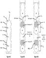
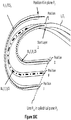
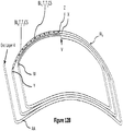
- the field-generating winding configurations for such applications in most cases, consist of multiple saddle shaped layers of winding. Each layer comprises multiple turns of winding as shown in Figures 1A and 1B .
- the shape of the saddle coil winding closely matches the shape of the cylindrical beam tube.
- Such saddle-shaped winding configurations for generating magnetic fields with a given pole number are typically produced by winding the conductor over itself and around a central island.
- the present invention is based, in part, on recognition that definition of the winding configuration in a saddle coil magnet (i.e., the conductor path) and accuracy of conductor placement in the winding configuration are critical to acquiring satisfactory or optimal field uniformity, especially in the case of superconducting windings.
- Other applications of magnetic fields, which are unrelated to charged particle beam optics, also have potential for improved performance based on improved field uniformity.
- improvements can be realized based on definition of more optimal winding configurations and positioning of the coil conductors to substantially conform to defined configurations in order to produce magnetic fields with acceptable high field uniformity.
- a feature of the invention is that performance of superconducting electrical machines, which provide unmatched power density, can be improved based on more optimal definition of wiring configurations to improve the quality of the magnetic fields.
- the field uniformity is largely determined by the accuracy of and stability in placement of the coils.
- a series of conductor assemblies are provided of the type which, when conducting current, generates a magnetic field or which, in the presence of a changing magnetic field, induces a voltage.
- a conductor having a spiral configuration is positioned along a path in a cylindrical plane.
- the conductor extends along an axis central to the cylindrical plane, and positions along the path vary in azimuthal angle.
- the azimuthal angle of each position is measurable in a plane orthogonal to the axis and relative to a reference point in the plane orthogonal to the axis.
- the configuration comprises a continuous series of connected turns, T n , for which n is an integer ranging from one to N.
- Each turn, T n includes a first arc, a second arc and first and second straight segments connected to one another by the first arc.
- the second arc connects the turn, T n , to an adjoining turn, T n+1 or T n-1 .
- each of the first and second straight segments in a turn T n is spaced apart from an adjacent parallel segment in an adjoining turn T n+1 or T n-1 .
- the azimuthal angle of each position is measurable in a plane orthogonal to the axis and relative to a reference point in the plane orthogonal to the axis, and the configuration comprises a continuous series of connected turns, T n .
- Each turn, T n includes a first arc, a second arc and first and second parallel segments connected to one another by the first arc.
- the second arc connects each turn, T n , to an adjoining turn, T n+1 or T n-1 .
- a second groove may be formed in the support body, also centered about the axis and spaced away from the first groove, such that at least the first spiral configuration is positioned in the first groove and at least one additional spiral configuration is positioned in the second groove.
- a conductor assembly in another set of embodiments, includes a body having a first channel formed therein defining a first path extending along a first cylindrical plane and along a direction parallel to an axis central to the cylindrical plane.
- the first channel is in a configuration comprising a continuous series of connected turns, GT j , providing a first spiral pattern.
- a length of conductor comprises two or more electrically connected segments each positioned in the first channel, with a first segment of the conductor positioned in the first cylindrical plane.
- the first segment provides a first layer of the conductor closest to the axis.
- Each of the other segments provides an additional layer, with each additional layer positioned over another layer.
- the body of the conductor assembly may include a second channel formed therein defining a second path extending along a second cylindrical plane and along a direction parallel to an axis central to the cylindrical plane, with the second channel in a configuration comprising a continuous series of connected turns, GT j , providing a second spiral pattern wherein the length of conductor extends from the first spiral pattern into the second spiral pattern with another segment of the conductor positioned in the second channel.
- a segment of the conductor positioned in the second channel may be positioned as a first layer of the conductor in the second channel, with the assembly including one or more additional segments of the conductor in the second channel with each segment in the second channel providing an additional layer of the conductor positioned over another layer of the conductor.
- Each layer of the conductor may be positioned in a different concentric plane about the axis, and the conductor may be a splice-free wire comprising each of the segments.
- the body may be insulative, such as the type formed of a fiberglass resin composite material or may be a laminate structure comprising a metal body having an insulative layer formed thereon, or a metal body which receives insulated conductor to provide a helical wiring configuration.
- a conductor assembly is also provided in which a conductor having a spiral configuration is positioned along a path in a cylindrical plane and extends along an axis central to the cylindrical plane, with positions along the path varying in azimuthal angle, ⁇ n .
- the azimuthal angle of each position is measurable in a plane orthogonal to the axis and relative to a reference point in the plane orthogonal to the axis.
- the configuration comprises a continuous series of connected turns, T n , for which n is an integer ranging from one to N.
- Each turn, T n includes a first arc and a first straight segment.
- the configuration includes a spacing between at least one turn, T n , and an adjacent turn T n+1 or T n-1 . For a given value of n:
- a body has a first channel formed therein defining a first path extending along a first cylindrical plane and along a direction parallel to an axis central to the cylindrical plane (with positions along the path varying in azimuthal angle based on position along the axis) where the first channel is in a configuration comprising a continuous series of connected turns, GT j , providing a first spiral pattern.
- the configuration comprises a continuous series of connected groove turns, GT j , for which j is an integer ranging from one to N.
- Each turn, GT j includes a first arc, a second arc and first and second straight segments connected to one another by the first arc.
- the second arc connects the turn, GT j to an adjoining turn, GT j+1 or GT j-1 .
- a related method for constructing a conductor assembly of the type which, when conducting current, generates a magnetic field or which, in the presence of a changing magnetic field, induces a voltage includes providing a conductor having a spiral configuration, positioned along a path in a first cylindrical plane, which conductor extends along an axis central to the cylindrical plane, with positions along the path varying in azimuthal angle.
- the azimuthal angle of each position is measurable in a plane orthogonal to the axis and relative to a reference point in the plane orthogonal to the axis.
- the configuration comprises a first plurality of N turns, T n , connected to one another in a continuous series in the first cylindrical plane, with each turn, T n , including first and second coil ends which are each a portion of a turn not parallel with the axis.
- the step of providing the conductor having a spiral configuration includes providing, as a portion of the second end turn in the first of the turns, a segment which extends to an adjoining turn which segment continues the spiral configuration from the first of the turns to the adjoining turn.
- the step of providing a conductor having a spiral configuration includes positioning the path of the conductor to extend along the axis in a second cylindrical plane concentric with the first cylindrical plane, and the configuration further includes a second plurality of turns connected to one another in a continuous series in the second cylindrical plane, with positions in the second cylindrical plane varying in azimuthal angle.
- a segment is provided which extends from the first of the turns to one of the turns in the second cylindrical plane. This segment connects portions of the spiral configuration in the first cylindrical plane with portions of the spiral configuration in the second cylindrical plane.
- a length of conductor extends in a continuous spiral pattern in a first cylindrical plane extending along a central axis to create a saddle coil shape.
- the pattern comprises N turns, T n , with each turn having a fixed position in the same cylindrical plane, each turn including a pair of straight segments parallel to one another.
- the open shapes are spiral turns created by modifying the lengths of straight sections in closed shapes or by modifying the curvature imparted by the shape function F(x), with respect to position along the axis. This imparts a spiral shape that connects with a straight section in a portion of an adjacent conductor shape in the set of open shapes.
- a conductor is provided in a spiral configuration, positioned along a path in a first cylindrical plane, which conductor extends along an axis central to the cylindrical plane, positions along the path varying in azimuthal angle.
- the azimuthal angle of each position is measured in a plane orthogonal to the axis and relative to a reference point in the plane orthogonal to the axis.
- the configuration comprises a first plurality of N turns, T n , connected to one another in a continuous series in the first cylindrical plane, each turn, T n , including first and second coil ends which are each a portion of a turn not parallel with the axis.
- a method for constructing a conductor assembly of the type which, when conducting current, generates a magnetic field or which, in the presence of a changing magnetic field, induces a voltage
- the method includes inserting multiple layers of the conductor in the channel to conform each layer of the conductor to the spiral configuration, with each layer of the conductor positioned along a path in a different one of multiple concentric cylindrical planes, which paths extend along an axis central to the cylindrical planes, positions along the paths varying in azimuthal angle.
- Each layer in the configuration comprises a plurality of N turns, T n , connected to one another in a continuous series in the first cylindrical plane.
- Each turn, T n includes first and second coil ends which are each a portion of a turn not parallel with the axis, and, for a given value of n, each of the turns T n is spaced apart from an adjacent turn T n +1 or T n -1 .
- Paths are defined for straight portions of the channel or for curved portions of the channel, which result in path segments which deviate from ideal channel path segments, into which one or more segments of conductor turns in one or more conductor layers are placed.
- multipole content which would otherwise be present in a field generated by the spiral configuration, relative to a pure multipole field of order m (which would theoretically be generated by a configuration having an ideal cos(m ⁇ ) current distribution), is reduced by applying a numerical optimization technique which modifies the shapes of turns to more closely conform the field pattern generated by the spiral configuration to the pure multipole field of order m.
- the numerical optimization technique may modify the shapes of turns to more closely conform the field generated by the spiral configuration to the multipole field which would theoretically be generated by a configuration having an ideal cos(m ⁇ ) current distribution.
- a conductor assembly which comprises a body member having a series of spaced-apart, concentric channels formed therein, with each channel formed in a different one of multiple concentric cylindrical planes formed about a central axis.
- a conductor is positioned in each of the channels with multiple layers of the winding stacked in each channel.
- the conductor may be formed in a saddle coil spiral configuration.
- a series of concentric channels is formed about an axis of a body member, with each channel passing through a different cylindrical plane and extending in a radial direction away from the axis.
- Multiple layers of conductor are placed within each of the channels with each layer positioned in a different concentric cylindrical plane.
- the winding may be a continuous, splice-free element.
- a configuration is provided for a conductive winding of the type which, when conducting current, generates a magnetic field or which, in the presence of a changing magnetic field, induces a voltage.
- a conductor having a spiral shape comprising turns, T n is positioned along a path in a first cylindrical plane. The conductor extends along an axis central to the cylindrical plane, with positions along the path varying in azimuthal angle.
- Each turn, T n includes a first arc, a second arc and first and second straight segments.
- the first segment of the conductor in the first turn is an arc.
- the second segment of the conductor in the second turn may be an arc.
- the first segment of the conductor in the first turn may be a straight segment and the second segment of the conductor in the second turn may be a straight segment.
- a spiral channel is formed in a body comprising a continuous series of connected channel turns, GT n , positioned along a path in a first cylindrical plane, which channel extends along an axis central to the cylindrical plane, with positions along the path varying in azimuthal angle.
- Each turn, GT n includes a first arc, a second arc and first and second straight segments.
- a first turn GT n and a second turn GT n+1 or GT n-1 adjoin one another in the series.
- the third segment provides a path for a conductive segment to provide electrical connection between conductor in the first and second segments.
- the first segment of the channel in the first turn or in the second turn may be an arc or a straight segment.
- a conductor In another configuration for a conductive winding of the type which, when conducting current, generates a magnetic field or which, in the presence of a changing magnetic field, induces a voltage, a conductor has a spiral pattern comprising a first continuous series of connected turns positioned along a path in a first cylindrical plane, and at least a second continuous series of connected turns positioned along a path in a second cylindrical plane.
- the conductor extends along an axis central to the cylindrical plane, with positions along the path varying in azimuthal angle.
- Each turn includes a first arc, a second arc and first and second straight segments.
- the azimuthal angle of each position is measurable in a plane orthogonal to the axis and relative to a reference point in the plane orthogonal to the axis.
- the third segment provides electrical connection between the first and second segments.
- the first segment of the conductor in the first turn or in the second turn may be an arc or a straight segment.
- a spiral channel formed in a body includes a first continuous series of connected channel turns positioned along a path in a first cylindrical plane, and at least a second continuous series of connected channel turns positioned along a path in a second cylindrical plane, which channel extends along an axis central to the cylindrical plane. Positions along the path vary in azimuthal angle.
- Each channel turn includes a first arc, a second arc and first and second straight segments. The azimuthal angle of each position is measured in a plane orthogonal to the axis and relative to a reference point in the plane orthogonal to the axis.
- the first segment of the channel in the first turn or the second turn may be an arc or a straight segment.
- a method of fabricating a spiral winding structure includes defining a spiral shaped channel about an axis in a body to provide a path.
- a conductive material is conformed to the path of the spiral shaped channel, wherein m is an integer greater than zero, ⁇ n is an angle measured in a plane orthogonal to the axis and relative to a reference point in the plane orthogonal to the axis, x is a position along the axis, and F(x) varies in value along each arc between zero and one.
- a structure includes at least first and second layers positioned about one another and two or more conductor portions, each conductor portion positioned along a different one of the layers, the first of the conductor portions in a first cylindrical plane centered about an axis and the second of the conductor portions in a second cylindrical plane also centered about the axis, with the second plane a greater distance from the axis than the first cylindrical plane, wherein at least the first and second conductor portions are segments in a continuous conductive path extending from along the first of the layers to along at least the second of the layers.
- the conductive path is arranged so that when conducting current a magnetic field can be generated or so that when, in the presence of a changing magnetic field, a voltage is induced.
- the first and second conductor portions each have a spiral configuration positioned along the path in one of the cylindrical planes and each extend along the axis, with positions along the path varying in azimuthal angle.
- Each conductor portion comprises a continuous series of connected turns, T n , for which n is an integer ranging from one to N.
- Each turn, T n includes a first arc, a second arc and first and second straight segments connected to one another by the first arc.
- the second arc connects the turn, T n , to an adjoining turn, T n+1 or T n-1 .
- the first and second conductor portions are each positioned in a groove formed in one of the first and second layers which groove defines positions of each conductor portion along the path.
- each of the first and second straight segments in a turn T n may be spaced apart from an adjacent straight segment in an adjoining turn T n+1 or T n-1 .
- a configuration for a conductive winding includes a length of conductor and a spiral channel in which two or more layers of the conductor are positioned, one layer over another layer, the channel including a first series of N connected channel turns formed in a portion of a body, the turns positioned along a path so that the channel extends along an axis, the channel having a depth extending in a radial direction with respect to the axis to contain the two or more layers.
- the configuration may include J layers of conductor in the channel each electrically connected in series to another layer in the channel to provide one conductor having J*N turns.
- Each of the layers of conductor may be positioned in a different one of multiple concentric cylindrical planes about the axis.
- the conductor may be continuous and splice free.
- the configuration may include a second spiral channel in which two or more additional layers of the conductor are positioned, one layer over another layer, the second channel including a second series of connected channel turns formed in another portion of the body in a cylindrical plane positioned radially outward from the first series of connected channel turns with respect to the axis, the second channel having a depth extending in a radial direction with respect to the axis to contain the additional layers.
- the body in which the channel is formed may be a layer of insulative material or a layer of conductive material.
- a method of forming a conductive winding includes forming a spiral channel in a portion of a body in which two or more layers of conductor are to be positioned, one layer over another layer.
- the channel includes a first series of connected channel turns, with the turns positioned along a path so that the channel extends along an axis.
- the channel has having a depth extending in a radial direction with respect to the axis to contain the two or more layers, the turns each comprising a straight section of the channel path and a curved section of the channel path, wherein the straight sections are formed with parallel channel walls by cutting into the body with a saw blade.
- a length of conductor is positioned in the channel by laying one portion of the length over another portion of the conductor length to provide one conductive layer over another conductive layer.
- the step of cutting into the body with a saw blade may provide a cut in a single path or a single pass to define the entire depth of the channel instead of requiring multiple paths of a cutting tool to machine the full depth of the channel to accommodate two or more layers of the conductor.
- a method for securing multiple layers of conductor in a single channel is provided.
- a channel is formed in a spiral configuration comprising a series of channel turns with the channel having a restricted opening of a first dimension smaller than a thickness dimension of the conductor.
- a first portion of the conductor is pushed through the restricted channel opening with application of a force so that the channel receives the conductor to create a first level of conductor turns in the channel turns.
- a second portion of the conductor is also pushed through the restricted channel opening with application of a force so that the channel receives a portion of the conductor to create a second level of conductor turns in the channel turns.
- the step of pushing the first portion of the conductor through the restricted channel opening may expand or deform the dimension of the channel opening, allowing a portion of each conductor turn to be pushed through the opening, after which the dimension of the opening may revert from an expanded dimension to a size which is substantially the same as the first dimension.
- the thickness dimension of the conductor may be the smallest dimension of the conductor and the difference between the first dimension of the restricted opening and the thickness dimension of the conductor may be between seven and nine percent.
- a channel is formed in a spiral configuration comprising a series of channel turns with the channel having a restricted opening of a first dimension smaller than a thickness dimension of the conductor by providing a first cut to a body to create a first width for an opening in the channel through which portions of the conductor are received into the channel.
- the thickness dimension may be the smallest dimension of the conductor.
- a second cut is made to create a second width in the channel larger than the first width. The first cut and the second cut may each be created with a tool and each may be created with a different tool.
- the first cut may create the majority of the depth of the channel to receive multiple layers of conductor with one layer stacked over another layer. Also, the first cut may provide a uniform width along a path defined by multiple ones of the channel turns, and the second cut may create a second width in the channel larger than the first width without altering the width of the opening.
- a channel which has a spiral configuration comprising a series of channel turns with the channel having a restricted opening of a first dimension smaller than a thickness dimension of the conductor by providing a first cut to a body to create an initial opening. At least a portion of the channel with the initial opening has a first width and a portion of the interior of the channel also has the first width.
- the initial opening is covered with a layer of removable material and a second cut creates the restricted opening through the layer of removable material.
- the restricted opening has the second width which is smaller than the first width.
- the first cut and the second cut may each be each created with a different tool, and the first cut may create the majority of the depth of the channel to receive multiple layers of conductor with one layer stacked over another layer.
- the first cut may provide a uniform channel width along a path defined by multiple ones of the channel turns, and the second cut may provide a uniform width to the restricted opening along a path defined by multiple ones of the channel turns.
- a conductive winding is also of the type which, when conducting current, generates a magnetic field or which, in the presence of a changing magnetic field, induces a voltage.
- This configuration includes a length of conductor and a spiral channel which accommodates two or more layers of the conductor for positioning therein, with one layer positioned over another layer.
- the channel includes a series of connected channel turns formed in a portion of a body, with the turns positioned along a path so that the channel extends along an axis, the channel having a depth extending in a radial direction with respect to the axis to contain the two or more layers.
- the channel includes a series of shaped repository openings along walls of the channel.
- Each repository opening is positioned a different radial distance from the axis to provide a series of repository positions, with one or more of the repository positions positioned over another one of the repository positions.
- Each repository opening is of a dimension smaller than a thickness dimension of the conductor to restrict passage of the conductor into an adjoining repository position such that a force must be applied to push the conductor through the repository opening and into the repository position.
- each repository opening is positioned in a different one of several cylindrical planes concentrically positioned about the axis.
- the conductor may be a splice-free continuous length, with a different portion of the conductor occupying a different repository position to provide a series of winding turns in each of several cylindrical planes concentrically positioned about the axis.
- one or more of the repository spacers is formed in the channel walls.
- a spiral channel is created in a portion of a body, which channel accommodates two or more layers of conductor for positioning therein, one layer over another layer.
- the channel includes a series of connected channel turns formed in a portion of the body, and the turns are positioned along a path so that the channel extends along an axis.
- the channel has a depth extending in a radial direction with respect to the axis to contain the two or more layers, and the channel includes a series of shaped repository openings along walls of the channel, with each repository opening formed a different radial distance from the axis to provide a series of repository positions, with one or more of the repository positions positioned over another one of the repository positions.
- Each repository opening is of a dimension smaller than a thickness dimension of the conductor to restrict passage of the conductor into an adjoining repository position such that a force must be applied to push the conductor through the repository opening and into the repository position.
- Segments of the conductor are sequentially passed through one or more of the repository openings to place each segment in one repository position to create a multi-level helical winding path in a single groove.
- By sequentially passing segments of the conductor through the repository openings it is possible to position different levels of conductor segments in different spaced-apart cylindrical planes positioned about the axis.
- a space is provided between a first repository position and a second repository position. The space provides for heat exchange to serve as a cooling channel for conductor in the first and second repository positions.
- shaped repository openings are created along walls of the groove, which openings define repository positions for different layers of conductor placed in the groove and constrain movement of the conductor.
- a space is provided between a first repository position and a second repository position, and at least two segments of conductor are passed through one or more of the repository openings to position a first segment in the first repository position and to position a second segment in the second repository position.
- a space between the first repository position and the second repository position is retained without containing another segment of conductor positioned between the first and second segments.
- the space may provide for heat exchange and serve as a cooling channel for conductor in the first and second repository positions.
- the space may be formed in the shape of a repository opening and be positioned between the first repository opening and the second repository opening.
- a wiring assembly is configured as a series of spaced-apart spiral configurations of conductor with each configuration positioned in a different one of multiple cylindrical planes each centered about a common axis.
- Each spiral configuration includes a plurality of conductor turns.
- the step of configuring the wiring assembly includes positioning segments of the conductor to provide turn-to-turn transitions which connect turns in the same plane to form a multi-turn helical geometry in each plane.
- Conductor segments also extend out of the cylindrical planes to conductively connect pairs of spiral configurations of conductor in the adjoining cylindrical planes to form one continuous multi-level winding configuration.
- the step of positioning segments of the conductor to provide turn-to-turn transitions within each multi-turn helical geometry only positions each of extended conductor segments within the cylindrical plane in which the multi-turn helical geometry is disposed.
- the step of providing the turn-to-turn transitions to connect turns in each plane may form a multi-turn helical geometry in each plane.
- a wiring assembly according to the invention includes a series of spaced-apart spiral configurations of conductor with each configuration positioned in a different one of multiple cylindrical planes each centered about a common axis.
- Each spiral configuration comprises a plurality of conductor turns, wherein the conductor includes
- a wiring assembly of the type which, when conducting current, generates a magnetic field or which, in the presence of a changing magnetic field, induces a voltage is formed with a series of spaced-apart spiral configurations of conductor each positioned along a common cylindrical plane centered about an axis with each configuration having multiple layers of winding.
- a series of conductor segments provide electrical connections between one or more pairs of the spaced apart configurations. Layout of one or more pairs of the conductor segments which effect the connections measurably offset magnetic field magnitudes of order m generated by each conductor segment when the segments are conducting current.
- a winding configuration in an assembly of the type which, when conducting current, generates a magnetic field or which, in the presence of a changing magnetic field, induces a voltage, includes multiple layers of conductor where each layer is a helically shaped, comprising a conductive material formed along a different cylindrical plane. Each of the cylindrical planes is centered about a common axis wherein the conductive material in each layer is electrically connected to conductive material in the other layers to provide a multi-layer helical winding configuration.
- the winding configuration is in the shape of a saddle coil.
- Each helically shaped layer may comprise a series of connected turns of the conductive material and the turns may be spaced apart from one another.
- the winding configuration may be in the shape of a multilayer saddle coil and each helically shaped layer may comprise a segment of conductor machined or otherwise patterned into a layer of conductive turns of a saddle coil geometry, and contact surfaces of conductor segments in adjacent ones of concentric coil rows may come into direct contact with one another to effect current flow from layer to layer.
- Concentric coil rows may be laminate structures comprising a conductive material deposited thereon.
- Such laminated concentric coil rows may be cylindrically shaped bodies each comprising m spaced-apart winding configurations with each winding configuration approximating a cos(m ⁇ ) current density relationship as a function of position along each winding configuration, where m is an integer value greater than zero and ⁇ is an azimuthal angle measured about the axis.
- Each winding configurations may have a conductive material deposited thereon and patterned to form a helically shaped layer.
- a method for forming a superconductor in a channel having a spiral path comprising.
- Chemical precursor material for synthesizing the superconductor is placed in a tube.
- the tube containing the chemical precursor materials is placed in the channel.
- the precursor material is chemically reacted in the tube after the tube is placed in the groove to synthesize the superconductor in situ.
- the tube may comprise a combination of a barrier metal and a stabilizing metal.
- the superconductor is MgB2
- the tube comprises copper and a surface along the inside of the tube is plated with niobium.
- a method for fabricating a superconducting assembly which forms a superconducting material in situ during fabrication of a winding configuration.
- the assembly may, when conducting current, generate a magnetic field or, in the presence of a changing magnetic field, induce a voltage.
- precursor materials for synthesizing the superconducting material are mixed together in stoichiometric proportions.
- a plurality of channels are created in a support structure with each channel positioned along a different cylindrical plane but centered about a common axis, Each channel comprises multiple helically shaped turns connected to one another.
- the mixed precursor materials are placed in each of the channels and reacted to synthesize the superconductor in the channels.
- the superconductor material in each channel of helically shaped layer is electrically connected to superconductor material in another of the channels to provide a multi-layer helical winding configuration.
- Multiple ones of the channels containing the precursor material may be sequentially formed in different cylindrical planes about the axis and then simultaneously heated to create a series of concentric channels each filled with one or more superconductive segments of wire.
- the step of sequentially forming the channels may include:
- each of the channels as a groove in a layer of material, each groove having an opening into which the precursor material is placed; and after placing the precursor material in the groove, covering the opening with another layer of material which closes the opening and provides further material in which another channel can be formed.
- the precursor for synthesizing the superconducting material are mixed in stoichiometric proportions.
- a plurality of ports is created with each port positioned along a different cylindrical plane but centered about a common axis, with each channel comprising multiple helically shaped turns connected to one another.
- the mixed precursor materials are placed in each of the channels by causing the mixed precursor materials to flow into each port with a carrier liquid.
- the carrier liquid is allowed to evaporate so that the precursor materials build up along walls of the ports.
- the support structure is heated to chemically synthesize the superconductor material in the ports.
- the synthesized superconducting material may comprise MgB 2 .
- Another method for fabricating a superconducting assembly forms superconducting material in situ during fabrication of a winding configuration.
- An open channel is formed in a support structure followed by sequentially forming in the channel (i) a metal layer (e.g., copper) along a channel wall, (ii) a barrier layer (e.g., niobium) over the metal layer, and a first mixture of precursor materials in stoichiometric proportions over the barrier layer.
- the precursor materials are then heated to chemically synthesize a first layer of superconductor material in the channel.
- the mixture of precursor materials may be repeatedly injected, dried and compacted in the channel.
- the step of forming in the channel the mixture of precursor materials may include injecting a slurry containing the precursor materials in the channel.
- the method may also include forming over the first mixture of precursor materials an insulative layer, and then the repeating the steps of forming in the channel (i) a metal layer along a channel wall, (ii) a barrier layer over the metal layer, and a mixture of precursor materials in stoichiometric proportions over the barrier layer, followed by heating the precursor materials to form a second layer of superconductor material in the channel which is electrically isolated from the first layer of superconductive material.
- the method may include that step of sealing the channel with silicon oxide or ceramic material before progressing to next level.
- channels or ports may be formed with variable cross sections and the area in cross section of the superconductor material may be increased along curved portions of turns in helical wiring configurations to limit maximum current density or avoid reaching critical field levels when the assembly carries current through the superconducting material.
- Portions of support structures on which wiring configurations are formed may be insulative and incorporate ceramic or glass fiber material in a resin composite to modify the temperature characteristics or mechanical properties of the support structure.
- a configuration for a superconducting winding of the type which, when conducting current, generates a magnetic field or which, in the presence of a changing magnetic field, induces a voltage, includes a spiral channel which accommodates two or more layers of the superconductor material for positioning therein, one layer over another layer.
- the channel includes a series of connected channel turns formed in a portion of a body. The turns are positioned along a path so that the channel extends along an axis, the channel having a depth extending in a radial direction with respect to the axis to contain the two or more layers.
- the channel includes a series of shaped repository openings along walls of the channel, and each repository opening is positioned a different radial distance from the axis to provide a series of repository positions.
- One or more of the repository positions is positioned over another one of the repository positions, and each repository opening is of a dimension smaller than a thickness dimension of the conductor to be passed therethrough to restrict passage of each conductor into an adjoining repository position such that a force must be applied to push the conductor through the repository opening and into the repository position.
- the configuration includes
- the first segment of copper conductor may be a body of copper wire inserted into the first repository position, or deposited copper formed in the first repository position.
- the current density distribution in any cross section perpendicular to the central axis of symmetry of the coil system is a function of the azimuth angle ⁇ which function substantially follows a cos(m ⁇ ) current density distribution where m is a multiple order, i.e., an integer greater than zero. This will yield a substantially pure multipole field.
- a central axis of symmetry for windings in a saddle coil magnet is referred to herein as an X axis as commonly understood in a cylindrical coordinate system, or in a Cartesian coordinate system comprising three orthogonal axes X, Y and Z.
- the angle ⁇ is the azimuthal angle measured in a plane transverse to the X-axis.
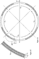
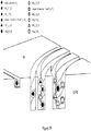
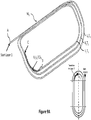
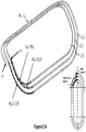
- An exemplary configuration of a quadrupole coil magnet 10 according to the invention is shown in Figure 2 , consisting of four interconnected saddle coil windings SC 1 , SC 2 , SC 3 and SC 4 , formed on a cylindrically shaped body 12 that surrounds a cylindrical aperture.
- the four saddle coil windings are formed along an exposed surface 20 of the cylindrically shaped body 12 and are symmetrically disposed about the X-axis, which is centrally positioned within the aperture. That is, the four saddle coil windings are spaced ninety degrees apart on center along the surface 20.
- the current density distribution has to be substantially proportional to the cosine of m times the azimuth angle, i.e., cos(m ⁇ ).
- designs for the winding of conductor around a central island have not been suitable for generating an optimum field uniformity, i.e., substantially in accord with a cos(m ⁇ )distribution.
- Embodiments of the invention introduce multiple spacers between individual turns of the coil winding to enable a controlled placement of a coil winding in substantial accord with an ideal cos(m ⁇ ) and thereby improve the current density distribution for superior field uniformity distribution over the full length of the coil.
- Double-helix coils as described in U.S. Patent No. 6,921,042 and U.S. Patent No. 7,864,019 , produce almost perfect cos(m ⁇ ) current density distributions over the central part of the winding configuration.
- double-helix windings do not produce pure multipole fields, since the coil ends do not obey the required cos(m ⁇ ) current density distribution.
- Coil turns that produce pure cos(m ⁇ ) current density distributions can be modeled.
- features of the invention are based on a recognition that conventional saddle coil layout and fabrication techniques are not well-suited for constructing saddle coil winding turns which are stable during operation and which sufficiently conform to these analytics.
- Embodiments of the invention are in recognition that the precision with which coil winding turns are positioned is highly determinative of whether fields can be generated with pure cos(m ⁇ ) current density distributions. According to one series of such embodiments it is possible to fabricate saddle coil configurations that satisfactorily replicate pure cos(m ⁇ ) current density distributions with the aid of multiple, discrete spacer elements positioned between adjacent winding turns over the full length of the coil.
- the spacer elements must be relatively complex and must vary, both in shape and thickness, in order to satisfactorily accommodate non-linear variations in coil position along the entire major axis of the saddle coil winding.
- continuous body material functions as a variably dimensioned continuous series of discrete spacers which securely define the paths of winding turns according to spacings between adjacent winding turns as required for the cos(m ⁇ ) current density distributions.
- the body material retains designated positioning of wiring turn conductor 14 under large Lorentz forces experienced during coil operation.
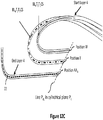
- conductor turns, T j , in each layer, L i are formed in a groove, and stacks of layers, L i , can be formed in the same groove.
- Multiple grooves, each comprising a stack of layers, L i are concentrically formed about a common axis, X.
- the described embodiment includes an arbitrary number of concentrically formed grooves, G. Specific reference to each of two illustrated grooves, G, is made by identifying the groove closest to axis, X, as groove G 1 , and the groove farthest from the axis, X, as groove G 2 .
- the turns, T j , of conductor 14 within each layer L i are each formed in a turn, GT j , of the groove, G.
- Stacks of conductor turns T j (each being a turn in a sequence of adjoining layers, e.g., L i , L i+1 , L i+2 , L i+3 ) can be formed or placed, one turn over another, in the same groove as illustrated in Figure 3B .
- the indexing of turns continues an alternating pattern of numbering which begins with the first turn T 1 at the outside of the spiral pattern in the third layer, and begins with the first turn T 1 at the inside of a spiral pattern in the fourth layer, and the alternating sequence continues for additional layers formed thereover.
- the outermost turn at the outside of the spiral groove pattern is always referred to as the groove turn GT 1 and the innermost turn at the inside of the spiral groove pattern is referred to as the groove turn GT n .
- the groove turns GT j are formed in a winding pattern that substantially meets the requirement of pure cos(m ⁇ ) current density as a function of azimuth angle ⁇ .
- the following methodology provides paths along the groove turns to which conductor winding configurations conform in multipole magnets of arbitrary order, n, (such as the quadrupole magnet 10) to yield almost perfectly pure cos(m ⁇ ) current density distributions over the entire length (where length is measured along the direction of the axis, X)of each saddle coil winding, i.e., including the end regions.
- the combination of this methodology with methods of assembly, such as illustrated for the magnet 10, enables fabrication of magnets with small aspect ratios and high field uniformities.
- a multipole saddle coil magnet of order n is generated with n identical saddle coil windings, SC k , symmetrically arranged around the circumference of the cylindrically shaped body 12 as shown for the quadrupole magnet 10 in Figures 2 and 3 .
- SC k saddle coil windings
- Equation 1 defines the angular distribution of those lines about the surface of the cylindrically shaped body on which a saddle coil is formed and which yield the cos(m ⁇ ) current density distribution.
- the length of these lines is arbitrary.
- Equation (1) can be solved for ⁇ n to obtain the azimuth angle of each turn in each layer W i .
- the four saddle coils W i of the quadrupole magnet 10 each spans an angular interval of 90 degrees along the circumference of the cylindrically shaped body 12 with the turn-to-turn spacing again defined by equation (1).
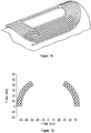
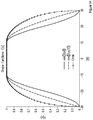
- Equation (2) Given these boundary conditions for the shape function, the values provided by equation (2) provide continuity between curved portions of the wiring path defined by the shape function and portions of the wiring path parallel with the axis, X, these being consistent with the cos(m ⁇ ) current density distribution. Examples of shape functions, F(x) are shown in Figure 14 . With reference to Equations (1) and (2) it is to be understood that any characterization of a turn, T n , or a spiral pattern constructed according to the invention as conforming to these equations refers to a conformity within reasonable fabrication tolerances.
- FIG. 2 An exemplary configuration of a quadrupole coil magnet 10 according to the invention is shown in Figure 2 , consisting of four interconnected saddle coil windings SC 1 , SC 2 , SC 3 and SC 4 formed on a cylindrically shaped body 12 that surrounds a cylindrical aperture.
- the four saddle coil windings are formed along an exposed surface 20 of the cylindrically shaped body 12 and are symmetrically disposed about the X-axis, which is centrally positioned within the aperture. That is, the four saddle coil windings are spaced ninety degrees apart on center along the surface 20.
- the groove paths and winding configurations obtainable according to Equation (1) and Equation (2) correspond to closed shapes. Accordingly, they do not describe the spiral nature of the conductor segments W i comprising multiple interconnected turns T j formed in the groove turns GT j in saddle coils according to the invention.
- Figure 18 illustrates a series of exemplary closed shapes 58 of conductor according to Equation (2). Modifications of the shapes 58 shown in Figure 18 can be computed numerically in a variety of ways to impart spiral shapes for the conductor 14 according to the invention. For example, the shape function can be spatially shifted while the length of a straight section of each turn GT j is shortened or lengthened to preserve continuity in the path function.
- the term turn, coil turn, or wiring turn refers to a conductor turn.
- a conductor turn may be a partial or a complete revolution of a conductor 14, e.g., wire, positioned in a spiral pattern along a cylindrical plane.
- a layer, L i comprises all turns formed along one cylindrical plane of a single saddle coil, or comprises all turns of multiple saddle coils formed about the same axis, i.e., along a cylindrically shaped plane defined by a fixed radial distance from a central axis of symmetry.
- the turns in a layer form one or more helical-like patterns typical of a saddle coil design.
- a dipole design may include two saddle coils, e.g., two distinct helical-like patterns, formed in the same cylindrical plane, with respect to the fixed radial distance from the central axis of symmetry.
- every portion of every turn in a winding layer precisely follow a path to effect a pure cos(m ⁇ ) current density distribution, or be entirely within a cylindrical plane.
- deviation from an ideal path may be required.
- wiring may be necessary for wiring to extend between different layers (i.e., between different cylindrical planes) as is the case when a multi-layer coil is fabricated with a single, continuous conductor 14. It may also be necessary for the wiring to depart from an ideal path in order to extend between ideal path portions of adjoining turns in the same layer.
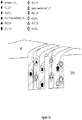
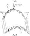
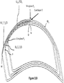
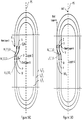
- Figure 3A is a perspective view of a quadrupole magnet during a stage of fabrication in which each of four saddle coils are built up with multiple layers of helical-like coil patterns formed one over another.
- the helical-like patterns can include asymmetries as may be required to achieve an ideal, or substantially ideal, cos(m ⁇ ) current density distribution.
- each saddle coil in the magnet of Figure 3A is formed in multiple layers, L i , of winding turns.
- each layer of the groove, G 1 comprises fifty two helical turns and each layer of the groove, G 2 , comprises fifty four helical turns.
- Each layer, L i is formed along a different one of several concentric cylindrical planes.
- each of the layers, L i in each saddle coil can, as shown in Figure 3A , be formed in a layer of insulative material by cutting a groove in the layer of insulative material.
- multiple adjoining layers of wire turns are placed one over another in one continuous groove, G.
- Multiple such grooves, G, each containing multiple adjoining layers of helical wire turns, are formed, one over another, with each groove formed in a different layer, or sublayer, of the insulative material.
- the grooves, G are each formed in a separate level or layer of insulative material. With the groove are formed to such depth that turns of four different layers, L 1 , L 2 , L 3 and L 4 , of the helically wound wire are stacked, one over another, the layers of helical turns create a multi-level winding with one continuous wire element having a substantially circular cross section of substantially constant radius.
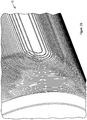
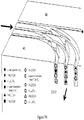
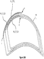
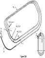
- the partial view of Figure 3B is a view in cross section of the four layers placed in one groove of the saddle coil of the magnet shown in Figure 3A .
- the view of Figure 3B is taken along a plane orthogonal to the central axis about which the saddle coil magnet is formed. The orthogonal plane passes through a straight portion of the helical turns of the coil.
- Figure 3B The exemplary view of Figure 3B is taken within a region of the saddle coil indicated by a circle in Figure 3A to illustrate eleven winding turns positioned in each of the four layers L i of conductor segments W i in the groove G1.
- the groove, G 1 contains two hundred and eight winding turns among four layers of the winding in the saddle coil SC 1 of the magnet 10.
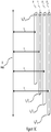
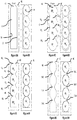
- Figure 3C is a simplified view in cross section along the path of a straight portion of a groove formed in the region enclosed by the circle, C, illustrating relative positions of four concentric cylindrical planes, P i (i.e., P 1 , P 2 , P 3 and P 4 ). All of the cylindrical planes, P i , are concentrically centered about a common axis, X. Each of the four planes passes through one groove. G, and each in the sequence of consecutive layers L 1 , L 2 , L 3 and L 4 of helical turns extends along a different one of the cylindrical planes. For example, layer L 1 extends along the plane P 1 and, generally, layer L i extends along a plane P i .
- the axis, X extends in a Cartesian (i.e., flat) plane (not illustrated) and along a straight line.
- the radial distance between each of the cylindrical planes P i and the axis, X, is R i .
- the view of Figure 3C is taken along the Cartesian plane in which the axis, X, extends, and through the four cylindrical planes P i .
- the plane also passes through straight portions of adjoining turns of the groove, G 1 , to illustrate relative positioning of stacked segments in each of the helical wire turns, T j , positioned in the groove, G 1 .
- Each turn is in a different one of the four layers, L i , of fifty two helically wound wire turns.
- Each of the illustrated stacked segments of a wire turn, T j is positioned at a different radial distance from the central axis, X.
- transitions between turns, T i , in adjacent layers, L i , L i+1 , and transitions between turns, T j , in the same layer, L i can be effected with two types of transition conductor segments TCS:
- the Bridge intraLayer T ransition C onductor S egments, IL i TCS, are portions of a wire conductor segment, W i , which extend between adjoining turns T j and T j+1 in a layer L i .
- the two types of transition conductor segments, TCS are portions of several wire conductor segments, W i , which form part of one continuous conductor 14 in the entire saddle coil winding of the quadrupole magnet shown in Figures 3 .
- each transition conductor segment TCS is positioned in a transition groove segment, TGS, which extends between two positions along the groove, G, in order to route wire formed in one turn in the groove, G, to a next turn formed in the same groove.
- transition groove segments, TGS carry the transition conductor segments (TCS) (i) between turns T j ,T j+1 within each layer, L i , of the conductor winding; or (ii) between adjoining layers, e.g., L i , L i+1 , of the conductor winding.
- transition groove segments, TGS which carry the transition conductor segments between turns within the same layer L i are referred to as Bridge Transition Groove Segments BL i T j T j+1 TGS.
- Groove segments, TGS, which carry conductor 14 between adjoining conductor layers Li,Li+i in a groove, G, are referred to as InterLayer Transition Groove Segments IL i L i+1 TGS.
- the transition conductor segments TCS are each routed along one of two types of transition groove segments to:
- the Bridge intraLayer Transition Conductor Segments BL j T j T j+1 CS are positioned in Bridge Transition Groove Segments BL i T j T j+1 TGS and the interlayer transition conductor segments IL i L i+1 TCS are positioned in Interlayer Transition Groove Segments, IL i L i+1 TGS.
- a transition groove segment, TGS can define a segment of the conductor winding path which substantially conforms with a desired cos(m ⁇ ) function to support an overall desired cos(m ⁇ ) current density distribution for the entire saddle coil winding.
- the transition groove segment, TGS may substantially depart from the winding path which conforms with a desired cos(m ⁇ ) function but adverse effects may be tolerable or negligible.
- Bridge intraLayer Transition Conductor Segments are portions of turns which connect adjoining turns, T j , in the same layer L i .
- a Bridge intraLayer Transition Conductor Segment, BL i T j T j+1 CS is routed along a Bridge Transition Groove Segment, BL i T j T j+1 GTS, which extends between positions on different groove turns, GT j , in the same groove, G.
- Each Bridge intraLayer Transition Conductor Segment BL i T j T j+1 CS is positioned in a Bridge Transition Groove Segment, BL i T j T j+1 TGS, to carry conductor 14 from turn to turn within the layer Li and provide electrical continuity between adjoining turns in the layer L i of conductor winding.
- the Bridge Transition Groove Segments provide paths along which portions of conductor 14 (i.e., the Bridge Intralayer Transition Conductor Segments, BL i T j T j+1 CS), are placed to transition the conductor 14 within one layer, L i , between different groove turns, GT j , in the same groove, G.
- each Bridge Transition Groove Segment BL i T j Tj +1 GTS, extends between a first position in one groove turn GT j and a second position in an adjoining groove turn, i.e., GT j+1 or GT j-1 , of the same groove.
- Interlayer Transition Conductor Segments are each positioned in an InterLayer Transition Groove Segment, IL i L i+1 TGS j , (i.e., where optional inclusion of subscript j denotes the groove turn GT j from which the Interlayer Transition Groove Segment extends to a next level L i .
- Such transitions between layers may be had by providing a path in an InterLayer Transition Groove Segment, IL i L i+1 TGS, which, as the path progresses, increases in radial distance from the distance R i (i.e., from the axis, X) associated with one cylindrically shaped plane, P i , to a radial distance R i+1 (i.e., also from the axis, X) associated with the next cylindrically shaped plane P i+1 .
- InterLayer Transition Conductor Segment IL i L i+1 TCS in an InterLayer Transition Groove Segment, IL i L i+1 TGS j , enables the conductor 14 to extend in a direction away from the axis, X, and between one cylindrically shaped plane P i and a next cylindrically shaped plane P i+1 such that the conductor wire may then continue, extending along the plane P i+1 in the layer L i+1 , directly over other portions of conductor winding positioned in the plane P i , i.e., in the underlying layer, L i .
- the turns, T j , of conductor 14 within each layer L i are each shown formed in a turn, GT j , of the groove, G.
- GT j the groove turn
- the majority, or the entirety, of each groove turn GT j , in which conductor is placed substantially conforms to a path which complies with the same cos(m ⁇ ) function required for conductor 14 placed therein to generate a current density distribution which substantially conforms to a cos(m ⁇ ) function.
- the conductor winding comprises a series of turns T j , wherein the majority or the entirety of each conductor turn conforms to a path within a groove turn which constrains the conductor 14 to generate a current density distribution substantially in accord with a predefined cos(m ⁇ ) function.
- a series of helical wire turns, T j each extend along the groove to form a spiral conductor winding in a layer, Li, at a distance R i from the axis, X.
- a first segment W 1 of the conductor extends in and along the groove to form the first layer, L 1 , comprising a series of helical conductor turns T j at a distance R 1 from the axis, X.
- a second segment W 2 of the conductor extends over the first segment W 1 , in and along the groove to form the second layer, L 2 , of helical turns at a distance R 2 from the axis, X.
- a third segment W 3 of the conductor extends over the first and second segments W 1 , and W 2 in and along the groove to form the third layer, L 3 , of helical turns at a distance R 3 from the axis, X.
- a fourth wire segment W 4 of the conductor extends over the first, second and third segments W 1 , W 2 and W 3 in and along the groove to form the fourth layer, L 4 , of helical turns at a distance R 4 from the axis, X.
- each of the layers which comprises an InterLayer Transition Conductor Segment IL i L i+1 TCS j
- the majority of the conductor in each layer is in a cylindrical plane and distanced from the axis, X, such that R 1 ⁇ R 2 ⁇ R 3 ⁇ R 4 .
- a stack of helical wire turns, T j each associated with a different layer L i , is positioned in a groove, G. See Figure 3C which illustrates segments of the turns, T j , which may be in spaced apart relation or may be in contact with adjacent wire turns T j .
- the wire segments are electrically insulated from one another.
- helical wire turns, T j of different layers in a single groove, to create a stack of conductor segments W i , e.g., segments of wire
- the conductor 14 is preformed (i.e., pre-manufactured) wire that must be securely placed in a series of groove turns.
- the preformed wire is placed so that the majority of each turn substantially conforms to a cos(m ⁇ ) function and remains stable in accord with the function during operation of the saddle coil magnet.
- the groove, G for containing a stack of helical conductor turns, T j , can sequentially receive each conductor segment, W i , to form the stack of turns, T j in the groove.
- the wire conductor segment, W i , of each layer, L i is securely positioned to stay in the groove, e.g., without movement of the wire out of the groove during fabrication and without unacceptable movement of the conductor 14 during operation of the coil magnet.
- a groove, G is machined in the surface 40 of a cylindrically shaped layer or sublayer 42 of insulative material centered about the axis X (shown in Figure 3C ).
- the insulative material may, for example, be an epoxy resin composite material, but the material may be ceramic or other insulative material.
- the groove, G is illustrated as having parallel walls 50, 52, rendering the general shape of the groove rectangular, but the actual shape of the groove will depending on the cutting process.
- a suitable grove extends from the surface 40 inward toward the axis, X, of the cylindrical planes P i (see Figure 3C ), but numerous features can be incorporated within the groove to accommodate different types of conductor 14 and to enhance stability or desired positioning of the conductor.
- the conductor segments W i of wire used to place helical turns T j of conductor 14 in the groove, G may have a circular shape in cross section. That is, at any point along the length of the helical winding, when viewed in a plane transverse to the direction along which the conductor segments W i extend, the shape of the wire is circular, having a characteristic diameter, D.
- the groove has a restricted opening 46 along the surface 40.
- the restricted opening 46 is somewhat smaller than the diameter D.
- the width of the opening maybe 0.74 mm.
- Figure 8B illustrates the groove design of Figure 8A with four conductor segments W i inserted therein.
- the shape of the conductor segments may vary and may, for example, be rectangular, elliptical or in the form of a ribbon.
- the size of the adjoining groove opening reverts from the expanded dimension substantially back to the original dimension. That is, the reversion from the expanded dimension results in a restricted opening size suitable for containing the wire during and after completion of subsequent fabrication steps.
- the difference between the size of the opening 46 and the diameter of the wire may be on the order of seven to nine percent.
- the opening With a circular shaped wire having a diameter in cross section of 0.8 mm, the opening may be in the range of 0.735 to 0.745 mm, e.g., 0.74 mm or 92.5 percent of the wire diameter. More generally, the difference between the size of the opening 46 i and the wire diameter may be in the range of 85 percent to 95 percent of the wire diameter.
- the difference between the size of the opening 46 and the smallest dimension of the wire may be on the order of seven to nine percent.
- the design of the groove, G can vary and may be specific to the size or shape of the wire being inserted as well as whether the wire is insulated. If the wire is not insulated, the shape of the groove can be designed to provide electrical separation of adjacent turns T j stacked in the groove.
- Figure 8C illustrates a groove as it may appear after being formed with a cutting tool
- Figure 8D illustrates placement of conductor segments in repository positions, RP i , of the groove to secure the conductor in place.
- a groove is initially formed with a first rotating cutting tool which provides the opening 46, having a first width, along the surface 40, while also forming interior surfaces, i.e., a major portion, of the groove with a substantially rectangular shape, also of the first width.
- the first cutting tool may initially penetrate the surface 40 in a downward direction (i.e., toward the axis, X) perpendicular to the surface, thereby cutting into the cylindrically shaped layer of insulative material to a predetermined depth.
- the first cutting tool then progresses along the surface 40 to cut the groove, G, along the cylindrical planes P i and thereby extend the initially formed opening along a groove path to define the groove turns GT j .
- a second rotating cutting tool having a slightly larger blade diameter than that of the groove opening 46 of the first width, enters the already formed groove to redefine major portions of the groove to a second width without altering the opening 46.
- the opening 46 retains the first width dimension while major portions of the groove, are expanded so that distances between opposing walls of the groove correspond to a second width. This resizing of the major portions of the groove to widen the width of the groove can be effected with a side entry into portions of the groove.
- the tool After the blade of the second cutting tool enters the groove from one position along the surface 40 of the groove, the tool is then moved through the groove to remove additional insulative material from the inside of the groove without cutting into or otherwise affecting the size of the opening 46. Consequently, interior portions of the initially formed groove are enlarged while not enlarging the opening 46 relative to the first width.
- the opening 46 remains as formed with the first cutting tool, while the interior of the groove is expanded to a second width larger than that of the first width, the second width being suitable for movement of the wire within the groove for purposes of placing and securing each coil turn T j within a corresponding groove turn GT j .
- a CNC machine instead of performing the step to widen the interior of the groove to a rectangular-like shape having a uniform second width, except, perhaps, at the bottom of the groove, a CNC machine can be programmed to pass a smaller cutting tool through the groove multiple times at a series of depth positions to define each in a series of variable width shaped repository positions.
- the smaller cutting tool is patterned to yield a series of circular profiles as the variable width shaped positions when widening the groove. That is, with each pass of the smaller cutting tool through the groove, each pass being at a different groove depth relative to the surface 40, the depth of the smaller tool within in the groove defines a shaped wire repository position RP i at a different radial distance R i from the axis, X, to receive a corresponding wire conductor segment, W i , for placement therein.
- Each repository position RP i occupies a position in a stacked sequence within the groove, G, such that the first and lower-most repository position RP 1 is a distance R 1 from the axis, X, the second repository position RP 2 in the sequence is a distance R 2 from the axis, X, the third repository position RP 3 in the sequence is a distance R 3 from the axis, X, and the fourth repository position RP 4 in the sequence is a distance R 4 from the axis, X.
- R 1 ⁇ R 2 ⁇ R 3 ⁇ R 4 is a distance R 1 from the axis, X.
- each wire conductor segment, W i can be locked into one in a stack of shaped repository positions, RP i , of varying width formed within the groove, G.
- Each wire conductor segment, W i is positioned a desired distance R i from the axis, X.
- Each wire conductor segment, W i also follows along a path in the groove which conforms to a cos(m ⁇ ) distribution, to yield a sufficiently pure multipole field.
- the cutting tool may be patterned to simultaneously cut all of the shaped positions in a single pass of the cutting tool through the groove.
- each segment of wire W i can be securely locked in place to facilitate assembly of each layer L i , and to further assure stability during operation of the saddle coil.
- Figures 8D and 8F which each illustrate four layers of conductor segments W 1 , W 2 , W 3 , W 4 positioned in the four repository positions RP i of the groove, G.
- each repository position, RP i in the groove, G is bounded by a repository opening 46i fashioned like the single restricted groove opening 46 shown in Figure 8A .
- Each conductor segment W i enters the groove by being pushed through an uppermost opening (e.g., opening 46 4 shown in Figure 8B ) from along the surface 40. See, also, Figures 8G and 8H , further discussed herein, which illustrate a design where shapes of spaced apart repository openings facilitate secure positioning of insulated wire used to form the conductor segments W i . Stabilization is further achieved by removal of gaseous pockets from the groove after the insertion of the conductor segments W i . By way of example, removal of the pockets can be effected by vacuum impregnation with an epoxy resin that is part of a wet lay-up applied as an overlay. The magnet may be placed in a vacuum bag to facilitate movement of the resin to fill voids. The operation may be performed in an autoclave which elevates temperature and pressure to effect curing while the vacuum is sustained in the bag.
- each repository opening 46 i occupies a position along a different one of the repository positions, RP i , in the stacked sequence of repository positions, such that a lower-most and first repository position opening 46 1 provides entry into the first repository position, RP 1 , a second repository position opening 46 2 provides entry into the second repository position, RP 2 , a third repository position opening 46 3 provides entry into the third repository position, RP 3 , and a fourth and upper-most repository position opening 46 4 along the surface 40 provides entry into the upper-most and fourth repository position, RP 4 .
- the four repository openings are in a stacked sequence such that during assembly the segment of wire W 1 is pushed through all four of the repository openings 46i and placed in the lower-most repository position, RP 1 .
- the segment of wire W 2 is pushed through three of the repository openings 46 2 , 46 3 and 46 4 and is placed in the second repository position, RP 2 ;
- the segment of wire W 3 is pushed through two of the repository openings46 3 and 46 4 and is placed in the third repository position, RP 3 ;
- the segment of wire W 4 is pushed through the repository opening 46 4 and placed in the fourth repository position, RP 4 . See Figures 8D and 8F .
- Each of the repository openings 46i is defined by one of the restrictive repository spacers RSi that has been machined within the groove for controlling movement of each conductor segment W i and each segment of wire W i can be securely locked within a different RP 3 repository position.
- the conductors can be bonded in the grooves. This can be achieved by a wet wound winding process and/or vacuum impregnation.
- each wire conductor segment, W i is pushed through a restricted opening as described for the opening 46 in Figure 8A . That is, each repository opening 46i is a restricted opening with respect to the diameter of the wire being inserted there through, being slightly smaller than the wire diameter.
- each restricted repository opening 46i is a restricted opening with respect to the diameter of the wire being inserted there through, being slightly smaller than the wire diameter.
- each turn, T j of the conductor segment, W i , into the groove to follow the helical winding path of each groove turn GT j .
- the individual portions of each wire turn, T j are pushed against edges of the groove which border the restricted opening 46i of each repository position RP i .
- Application of the force temporarily expands or deforms the dimension of the opening 46i, allowing the portions of each turn, T j , to be pushed through the opening 46i in order to receive portions of the wire into the groove.
- the size of the adjoining restricted opening reverts from the expanded dimension substantially back to the original dimension.
- the difference between the size of the opening 46i and the diameter of the wire may be on the order of seven to nine percent.
- the width of the opening may be in the range of 0.735 to 0.745 mm. More specifically, a wire diameter of 0.8 mm, the opening may be 0.74 mm or 92.5 percent of the wire diameter.
- the restricted repository openings 46i are all the same size as the opening 46 illustrated in Figure 8A , and the wire conductor segment, W 1 , passes through all four openings 46 1 , 46 2 , 46 3 and 46 4 in order to occupy the lowest shaped position (i.e., the repository position, RP 4 ) as the lowest wire in the stack of helical windings to create the layer L 1 .
- the wire W 4 only passes through the upper most opening 46 1 (along the surface 40).
- the groove design of Figures 8C and 8E may be further modified to accommodate cooling channels or to accommodate spaced-apart (e.g., uninsulated) wire conductor segments W i .
- neck openings 56A through 56C are formed to provide a spacer function between adjacent wires, W i .
- the neck openings extend in the radial direction, i.e., in directions parallel with lines extending from the axis, X, and through the groove, G.
- the neck openings 56A through 56C are deformable as in the example designs shown in Figures 8A through 8F for the openings 46 and 46 1 through 46 4 , but for a given wire diameter the width of the neck openings may differ from that of the restricted repository openings 46i of Figures 8C and 8E in order to provide ability of the material about the neck openings to undergo deformation to accommodate the wire diameter and then resiliently return to an original width.
- each conductor segment W i may be pushed through one or more of the neck openings and then be locked within a shaped position of varying width to form a layer L i which is spaced apart from each adjacent layer. See Figure 8H .
- the spaces between layers L i may be used as cooling channels through which cooling liquid or gas may circulate to remove heat from the saddle coil.
- the design of the groove, G can be created by first cutting the entire groove to a nominal second width required for the conductor placement, e.g., with the above-referenced second tool. At this stage, the groove opening 46 is not smaller than the width along interior portions of the groove. Next, the opening 46 and the adjoining surface 40 are covered with a thin overwrap layer of uncured epoxy resin impregnated glass tape.
- This overwrap does not have to cover the entire length of the groove, but can be limited to a few sections, mainly near bends or arcs in the path which the groove follows, as this is where the conductor may have a tendency to not stay well positioned in the groove during the winding process.
- the material can be cut on a CNC machine to re-create the groove opening with a small cutter or router bit, e.g., with the above-referenced first tool, the opening having the above-referenced first width for a restricted opening 46 while the interior of the groove continues to be of a second width, e.g., created with the above-referenced second cutting tool, so that the second width is larger than the first width.
- Figures 4A through 4D are unrolled views of a fabrication sequence for constructing saddle coils according to the invention with four conductor segments, W i , each configured as a layer, L i , with i ranging from 1 through 4.
- W i conductor segments
- L i layer
- i ranging from 1 through 4.
- a transition section of winding wire and a crossing section of winding wire are each provided to initiate and continue placement of the winding wire of a subsequent layer over a winding wire of a previous layer so that each of the second, third and fourth segments of the continuous winding wire can be positioned over a prior placed segment of the continuous winding wire.
- Figures 4A through 4D illustrate principles of a generic fabrication sequence applied to an exemplary one of multiple (e.g., four) saddle coils SC k formed about the axis, X.
- the exemplary saddle coil SC k is formed about a Cartesian (i.e., flat) plane of symmetry, PS, which passes through the axis, X.
- the generic fabrication sequence can be applied to form each of four saddle coil layers L i of conductor in one groove, G, in saddle coil windings such as shown in Figure 3B .
- each layer, L i is formed with a conductor segment, W i , configured as a series of layers, L i , each comprising only three helical turns, each being formed in or about a cylindrically shaped plane P i centered about the axis X.
- the principles can readily be applied the layers L i of the saddle coil shown in Figures 3 as well as saddle coils comprising an arbitrary and large number layers (e.g., i > 4) and turns (e.g., T j > 100) in each layer.
- the four layers of conductor are placed, one over another, in a groove, G, similar to the groove shown in Figure 8A or Figure 8C , as illustrated for one saddle coil winding of the quadrupole magnet shown in Figures 3B .
- a first length of the continuous winding wire is placed in the groove, G, to follow a helical (i.e., helical-like) path in or along one of multiple concentric cylindrically shaped planes in accord with a path defined by the groove.
- a helical i.e., helical-like
- Reference in this description to positions, e.g., positions Q and V shown in Figure 4C is with regard to positions along the paths defined by a groove, G, irrespective of whether the position resides in a particular cylindrical plane P i or layer L i formed in the groove.
- position is not limited to a single point, or a set of points in a single cylindrical plane, but can comprehend a series of points located at the same position along the trajectory of a path defined by the groove.
- a series of points that lay one over another in different cylindrical planes centrally positioned about the axis, X may be referred to as being at the same position along the groove, G.
- the third turn of the second layer is designated L 2 T 3 .
- placement starts at a position A and extends from the outside of the helical-like winding configuration (i.e., an outer-most turn in an outer region of the saddle coil) and winds inward in a spiral manner (e.g., in a clockwise direction) to complete three exemplary helical turns of the first layer L 1 , e.g., L 1 T 1 , L 1 T 2 , L 1 T 3 .
- the first turn L 1 T 1 is referred to as a turn but is not a complete 360° turn because it begins at the position A 1 instead of a point A' in the Cartesian plane of symmetry, PS.
- the first and second helical turns L 1 T 1 , L 1 T 2 and the majority of the third helical turn, L 1 T 3 are positioned in the cylindrical plane P 1 about which the layer L 1 is primarily formed.
- the majority of the layer L 1 is formed at a radial distance R 1 from the central axis, X.
- the third helical turn, L 1 T 3 which is the inner-most turn of the first layer L 1 , includes an InterLayer Transition Conductor Segment IL 1 L 2 TCS 3 (where S 3 designates that the segment is in the third turn of the layer L 1 ) that extends along the third turn from a position B and toward (e.g., up to) a position C.
- the segment IL 1 L 2 TCS 3 is indicated in the figures with a thickened line width relative to other portions of the third helical turn L 1 T 3 .
- the unrolled view of Figure 6A illustrates a view of the groove, G, along the path of the conductor segment W 1 , starting at the position A and spiraling inward.
- the coil layer segment W 1 is inserted in three turns GT 1 , GT 2 and GT 3 of the groove, G, primarily along the plane P 1 . That is, for an embodiment of the groove according to Figures 8B and 8C , the view of Figure 6A is taken through the repository position, RP 1 , of the groove, and along the first and second groove turns GT 1 , GT 2 as well as along the majority of the third groove turn, GT 3 , i.e., in the cylindrical plane P 1 about which the layer L 1 is primarily formed.
- Figure 6A also illustrates a segment of the groove, IL 1 L 2 TGS, referred to as an interlayer transition groove segment, in the third groove turn, GT 3 , that extends from the position B to the position C.
- the interlayer transition groove segment, L 1 L 2 TGS is indicated in Figure 6A with a thickened line width relative to other portions of the third groove turn GT 3 .
- a feature of the interlayer transition groove segment, L 1 L 2 TGS, is that it defines the path along which the interlayer transition conductor segment IL 1 L 2 TCS 3 extends from within the plane P 1 and up to the plane P 2 as shown in Figures 9 .
- the Interlayer Transition Conductor Segment IL 1 L 2 TCS 3 extends out of the cylindrical plane P 1 and up to the cylindrical plane P 2 to transition the helical wiring path from the conductor segment W 1 along the layer L 1 in order to begin a first turn L 2 T 1 of the conductor segment W 2 along the plane P 2 for the layer L 2 . Transitions of the Interlayer Transition Conductor Segment IL 1 L 2 TCS 3 out of the plane P 1 and toward the plane P 2 are further shown in the full and partial perspective views of conductor segment W 1 of Figures 9A- 9C .
- the perspective view of Figure 9B illustrates the rise in the segment IL 1 L 2 TCS 3 from the position B in the plane P 1 and toward the position C which is in the plane P 2 .
- FIG. 9C illustrates the position C along a line P 1L in the cylindrical plane P 1 .
- the winding process continues at the position C by placing the next portion in the continuous saddle coil winding, the conductor segment W 2 of the second helical layer L 2 , in the same groove, G, and over the first wire segment W 1 of the first layer L 1 . That is, placement of the segment W 2 of the second layer L 2 over the segment W 1 begins at position C and continues along a spiral path which winds outward from the inside of the helical-like winding configuration (e.g., continuing in a clockwise direction) to complete three exemplary helical turns of the second layer, e.g., L 2 T 1 , L 2 T 2 , L 2 T 3 .
- the first and second helical turns L 2 T 1 , L 2 T 2 and the majority of the third helical turn, L 2 T 3 , are positioned in the cylindrical plane P 2 about which the layer L 2 is formed, i.e., a radial distance R 2 from the central axis, X.
- the first and second helical turns L 2 T 1 , L 2 T 2 include a Bridge intraLayer Transition Conductor Segment BL 2 T 1 T 2 CS which follows a transition path defined by an intralayer bridge transition groove segment BL 2 T 1 T 2 TGS shown in Figure 6B .
- the Bridge intraLayer Transition Conductor Segment BL 2 T 1 T 2 CS is indicated in the figures with a thickened line width relative to other portions of the first and second helical turns L 2 T 1 and L 2 T 2 .
- the Bridge intraLayer Transition Conductor Segment BL 2 T 1 T 2 CS in the plane P 2 is also shown in the perspective views of Figures 10A - 10C .
- the Bridge Transition Groove Segment BL 2 T 1 T 2 TGS connects portions of the turns L 2 T 1 and L 2 T 2 in the groove, G, which each substantially conforms to a cos(m ⁇ ) function.
- the bridge transition groove segment BL 2 T 1 T 2 TGS extends between a point D of turn L 2 T 1 (in plane P 2 ) in the groove, G, and a point E of the turn L 2 T 2 (also in plane P 2 ) in the groove, G.
- This bridge transition groove segment BL 2 T 1 T 2 TGS is shown in Figure 6B .
- the Bridge Intralayer Transition Conductor Segment BL 2 T 1 T 2 CS thus follows a path which departs from the path of the groove turn GT 3 , which substantially conforms to a cos(m ⁇ ) function. That is, each of the groove turns GT1, GT2 and GT3 define a path which is consistent with a cos(m ⁇ ) function while the bridge transition groove segment BL 2 T 1 T 2 TGS departs therefrom in order to define a path for the Bridge intraLayer Transition Conductor Segment BL 2 T 1 T 2 CS which effects conductive connection between the two points D and E in the groove, G.
- the conductor segment BL 2 T 1 T 2 CS lies in the cylindrical plane P2 and is placed in intralayer bridge transition groove segment BL 2 T 1 T 2 TGS.
- the second and third helical turns L 2 T 2 , L 2 T 3 include a Bridge intraLayer Transition Conductor Segment BL 2 T 2 T 3 CS which follows a transition path defined by an intralayer Bridge Transition Groove Segment BL 2 T 2 T 3 TGS.
- the Bridge intraLayer Transition Conductor Segment BL 2 T 2 T 3 CS is indicated in the figures with a thickened line width relative to other portions of the first and second helical turns L 2 T 2 and L 2 T 3 .
- the Bridge intraLayer Transition Conductor Segment BL 2 T 2 T 3 CS in the plane P 2 is also shown in the perspective views of Figures 10A - 10C .
- the Bridge Transition Groove Segment BL 2 T 2 T 3 TGS provides a path which connects portions of the turns L 2 T 2 and L 2 T 3 which substantially conform to a cos(m ⁇ ) function.
- the Bridge Transition Groove Segment BL 2 T 2 T 3 TGS extends between a point F of turn L 2 T 2 (in plane P 2 ) in the groove, G, and a point H of the turn L 2 T 3 (also in plane P 2 ) in the groove, G, departing from this cos(m ⁇ ) relationship to define a path for the Bridge intraLayer Transition Conductor Segment BL 2 T 2 T 3 CS which effects conductive connection between the two points F and H in the groove, G.
- the Bridge intraLayer Transition Conductor Segment BL 2 T 2 T 3 CS thus follows a path which departs from a path which substantially conforms to the cos(m ⁇ ) function to effect conductive connection between the two points F and H.
- the conductor segment BL 2 T 2 T 3 CS lies in the cylindrical plane P2 and is placed in intralayer Bridge Transition Groove Segment BL 2 T 2 T 3 TGS.
- the Bridge Transition Groove Segment BL 2 T 2 T 3 TGS is shown in Figure 6B .
- the third helical turn, L 2 T 3 i.e., the outer-most turn of the second layer L 2 , includes an Interlayer Transition Conductor Segment, IL 2 L 3 TCS 3 , (where S 3 designates that the segment is in the third turn of the layer L 2 ) that extends between a position J and a position K.
- S 3 designates that the segment is in the third turn of the layer L 2
- the position K appears coincident with the position H in Figure 4B
- the position K is in the plane P 3 while the position H is in the plane P 2 .
- the Interlayer Transition Conductor segment, IL 2 L 3 TCS 3 is indicated in the figures with a thickened line width relative to other portions of the third helical turn L 2 T 3 .
- the InterLayer Transition Conductor Segment IL 2 L 3 TCS 3 extends out of the cylindrical plane P 2 and up to the cylindrical plane P 3 to transition the helical wiring path from the conductor segment W 2 along the layer L 2 in order to begin a first turn L 3 T 1 of the conductor segment W 3 along the plane P 3 for the layer L 3 . Transition of the segment IL 2 L 3 TCS 3 out of the plane P 2 and toward the plane P 3 is further shown in the perspective views of Figures 10A - 10C . Once the outer-most turn, e.g., T 3 , of the layer L 2 is placed in the groove, placement of the conductor segment W 2 of the continuous saddle coil winding wire extends up to the position K, rendering the second layer L 2 complete.
- FIG. 10A and 10B also illustrate the Bridge intraLayer Transition Conductor Segments BL 2 T 1 T 2 CS and BL 2 T 2 T 3 CS.
- the partial perspective view of Figure 10C illustrates the Bridge intraLayer segments BL 2 T 1 T 2 CS and BL 2 T 2 T 3 CS and the InterLayer Transition Conductor Segment IL 2 L 3 TCS 3 in relation to one another.
- Figure 10C also illustrates the positions D, F and J on the same line P 2L in the cylindrical plane P2 as well as position K in the cylindrical plane P 3 .
- the winding process continues through the position K by placing the next portion in the continuous saddle coil winding, which is the conductor segment W 3 of the third helical layer L 3 , in the same groove, G, and over the second wire segment W 2 of the second layer L 2 .
- Placement of the segment W 3 of the third layer L 3 over the segment W 2 begins at position K and continues along a spiral path which winds inward from the outside of the helical-like winding configuration (e.g., continuing in a clockwise direction) to complete three exemplary helical turns of the third layer: L 3 T 1 , L 3 T 2 , L 3 T 3 .
- the first and second helical turns L 3 T 1 , L 3 T 2 and the majority of the third helical turn, L 3 T 3 are positioned in the cylindrical plane P 3 about which the layer L 3 is primarily formed, i.e., a radial distance R 3 from the central axis, X.
- the first and second helical turns L 3 T 1 , L 3 T 2 include a first Bridge intraLayer Transition Conductor Segment BL 3 T 1 T 2 CS which follows a transition path defined by an intralayer Bridge Transition Groove Segment BL 3 T 1 T 2 TGS shown in Figure 6C .
- the Bridge intraLayer Transition Conductor Segment BL 3 T 1 T 2 CS is indicated in the figures with a thickened line width relative to other portions of the first and second helical turns L 3 T 1 and L 3 T 2 .
- the Bridge intraLayer Transition Conductor Segment BL 3 T 1 T 2 CS positioned in the plane P 3 , is also shown in the perspective views of Figures 11A - 11C .
- the Bridge Transition Groove Segment, BL 3 T 1 T 2 TGS provides a path which connects portions of the turns L 3 T 1 and L 3 T 2 in the groove, G.
- the turns L 3 T 1 and L 3 T 2 each follow a path that substantially conforms to a cos(m ⁇ ) function.
- the Bridge Transition Groove Segment, BL 3 T 1 T 2 TGS extends between a point M of turn L 3 T 1 (in plane P 3 ) in the groove, G, and a point N of the turn L 3 T 2 (also in plane P 3 ) in the groove, G.
- This Bridge Transition Groove Segment, BL 3 T 1 T 2 TGS is shown in Figure 6B .
- the Bridge intraLayer Transition Conductor Segment BL 3 T 1 T 2 CS thus follows a path which departs from the path of the groove turn GT 1 , which substantially conforms to a cos(m ⁇ ) function. That is, the bridge transition groove segment defines a path for the Bridge intraLayer Transition Conductor Segment BL 3 T 1 T 2 CS which departs from the cos(m ⁇ ) relationship to effect conductive connection between the two points M and N in the groove, G.
- the Bridge intraLayer Transition Conductor Segment BL 3 T 1 T 2 CS lies in the cylindrical plane P 3 and is placed in the intralayer Bridge Transition Groove Segment BL 3 T 1 T 2 TGS shown in Figure 6C .
- the second and third helical turns L 3 T 2 , L 3 T 3 include a Bridge intraLayer Transition Conductor Segment BL 3 T 2 T 3 CS which follows a transition path defined by an intralayer Bridge Transition Groove Segment BL 3 T 2 T 3 TGS.
- the Bridge intraLayer Transition Conductor Segment BL 3 T 2 T 3 CS is indicated in Figure 4C with a thickened line width relative to other portions of the second and third helical turns L 3 T 2 and L 3 T 3 .
- the Bridge intraLayer Transition Conductor Segment BL 3 T 2 T 3 CS positioned in the plane P 3 , is also shown in the perspective views of Figures 11A - 11C .
- the Bridge Transition Groove Segment BL 3 T 2 T 3 TGS connects portions of the turns L 3 T 2 and L 2 T 3 which substantially conform to a cos(m ⁇ ) function.
- the Bridge Transition Groove Segment BL 3 T 2 T 3 TGS extends between a point P of turn L 3 T 2 (in plane P 3 ) in the groove, G, and a point Q of the turn L 3 T 3 (also in plane P 3 ) in the groove, G, departing from this cos(m ⁇ ) relationship to define a path for the Bridge intraLayer Transition Conductor Segment BL 3 T 2 T 3 CS which effects conductive connection between the two points P and Q in the groove, G.
- the Bridge intraLayer Transition Conductor Segment BL 3 T 2 T 3 CS thus follows a path which departs from a path which substantially conforms to the cos(m ⁇ ) function to effect the conductive connection between the points P and Q.
- the conductor segment BL 3 T 2 T 3 CS lies in the cylindrical plane P 3 and is placed in intralayer Bridge Transition Groove Segment BL 3 T 2 T 3 TGS.
- the third helical turn, L 2 T 3 which is the inner-most turn of the third layer L 3 , includes a Bridge intraLayer Transition Conductor Segment BL 3 L 4 TCS 3 (where S 3 designates that the segment is in the third turn of the layer L 3 ) that extends between a position U in the plane P 3 and a position V in the plane P 4 . Although the positions V and Q appear coincident in Figure 8C , the positions are in different planes.
- the Bridge intraLayer Transition Conductor Segment BL 3 L 4 TCS 3 is indicated in the figures with a thickened line width relative to other portions of the third helical turn L 3 T 3 .
- the InterLayer Transition Conductor Segment IL 3 L 4 TCS 3 extends out of the cylindrical plane P 3 and up to the cylindrical plane P 4 to transition the helical wiring path from the conductor segment W 3 along the layer L 3 in order to begin a first turn L 4 T 1 of the conductor segment W 4 along the plane P 4 for the layer L 4 .
- Transition of the InterLayer Transition Conductor Segment IL 3 L 4 TCS 3 out of the plane P 3 and toward the plane P 4 is further shown in the perspective views of Figures 11A - 11C .
- FIG. 11A and 11B also illustrate the Bridge intraLayer Transition Conductor Segments BL 3 T 1 T 2 CS and BL 3 T 2 T 3 CS.
- the partial perspective view of Figure 10C illustrates the Bridge intraLayer Transition Conductor Segments BL 3 T 1 T 2 CS and BL 3 T 2 T 3 CS and the InterLayer Transition Conductor Segment, IL 3 L 4 TCS 3 , in relation to one another.
- Figure 10C also illustrates the positions M, P and U on the same line P 3L in the cylindrical plane P 3 as well as position V in the cylindrical plane P 4 .
- the winding process continues at the position V by next placing the next portion in the continuous saddle coil winding, which is the conductor segment W 4 of the fourth helical layer L 4 , in the same groove, G, and over the third wire segment W 3 of the third layer L 3 .
- Placement of the segment W 4 of the fourth layer L 4 over the segment W 3 begins at the position V and continues along a spiral path which winds outward from the inside of the helical-like winding configuration, e.g., continuing in a clockwise direction, to complete three exemplary helical turns of the third layer: L 4 T 1 , L 4 T 2 , L 4 T 3 .
- the first and second helical turns L 4 T 1 , L 4 T 2 and the majority of the third helical turn, L 4 T 3 , are positioned in the cylindrical plane P 4 about which the layer L 4 is primarily formed, i.e., a radial distance R 4 from the central axis, X.
- the first and second helical turns L 4 T 1 , L 4 T 2 include a Bridge intraLayer Transition Conductor Segment BL 4 T 1 T 2 CS which follows a transition path defined by an intralayer Bridge Transition Groove Segment BL 4 T 1 T 2 TGS shown in Figure 6D .
- the Bridge intraLayer Transition Conductor Segment BL 4 T 1 T 2 CS is indicated in the figures with a thickened line width relative to other portions of the first and second helical turns L 4 T 1 and L 4 T 2 .
- the Bridge intraLayer Transition Conductor Segment BL 4 T 1 T 2 CS positioned in the plane P 4 , is also shown in the perspective views of Figures 12A - 12C .
- the Bridge Transition Groove Segment BL 4 T 1 T 2 TGS connects portions of the turns L 4 T 1 and L 4 T 2 in the groove, G, which each substantially conforms to a cos(m ⁇ ) function.
- the Bridge Transition Groove Segment BL 4 T 1 T 2 TGS extends between a point W of turn L 4 T 1 (in plane P 4 ) in the groove, G, and a point X of the turn L 4 T 2 (also in plane P 4 ) in the groove, G. See Figure 6D .
- the Bridge intraLayer Transition Conductor Segment BL 4 T 1 T 2 CS follows a path which departs from a path of the groove turn GT 3 , which substantially conforms to a cos(m ⁇ ) function.
- the groove turn, GT 3 defines a path consistent with a cos(m ⁇ ) function while the Bridge Transition Groove Segment BL 4 T 1 T 2 TGS departs therefrom in order to define a path for the Bridge intraLayer Transition Conductor Segment BL 4 T 1 T 2 CS which effects conductive connection between the two points W and X in the groove, G.
- the Bridge intraLayer Transition Conductor Segment BL 4 T 1 T 2 CS lies in the cylindrical plane P 4 and is placed in the intralayer Bridge Transition Groove Segment BL 4 T 1 T 2 TGS.
- the second and third helical turns L 4 T 2 , L 4 T 3 include a Bridge intraLayer Transition Conductor Segment BL 4 T 2 T 3 CS which follows a transition path defined by an intralayer Bridge Transition Groove Segment BL 4 T 2 T 3 TGS.
- the Bridge intraLayer Transition Conductor Segment BL 4 T 2 T 3 CS is indicated in the figures with a thickened line width relative to other portions of the first and second helical turns L 4 T 2 and L 4 T 3 .
- the Bridge intraLayer Transition Conductor Segment BL 4 T 2 T 3 CS in the plane P 4 is also shown in the perspective views of Figures 12A - 12C .
- the Bridge Transition Groove Segment BL 4 T 2 T 3 TGS provides a path which connects portions of the turns L 4 T 2 and L 4 T 3 in the groove, G, which substantially conform to a cos(m ⁇ ) function.
- the Bridge Transition Groove Segment BL 4 T 2 T 3 TGS extends between the point W of turn L 4 T 2 (in plane P 4 ) in the groove, G, and a point X of the turn L 4 T 3 (also in plane P 4 ) in the groove, G, departing from this cos(m ⁇ ) relationship to define a path for the Bridge intraLayer Transition Conductor Segment BL 4 T 2 T 3 CS which effects conductive connection between the two points W and X in the groove, G.
- the Bridge intraLayer Transition Conductor Segment BL 4 T 2 T 3 CS thus follows a path which departs from a path which substantially conforms to the cos(m ⁇ ) function to effect conductive connection between the points W and X.
- the Bridge intraLayer Transition Conductor Segment BL 4 T 2 T 3 CS lies in the cylindrical plane P 4 and is placed in the intralayer Bridge Transition Groove Segment BL 4 T 2 T 3 TGS.
- the Bridge Transition Groove Segment BL 4 T 2 T 3 TGS is shown in Figure 6D .
- the third helical turn, L 4 T 3 which is the outer-most turn of the fourth layer L 4 , could include an Interlayer Transition Conductor Segment IL 4 L 5 TCS 3 (where S 3 designates that the segment is in the third turn of the layer L 2 ) if the illustrated saddle coil were to include a fifth layer Ls of conductor segment W 5 in a fifth cylindrical plane P 5 .
- the turn L 4 T 3 is the last turn in the saddle coil SC 1 before the conductor is routed to another saddle coil in the magnet 10.
- the turn L 4 T 3 is shown in the figures as a partial turn ending at point AA 1 (i.e., ending at the point AA 1 instead of a point AA' in the Cartesian plane of symmetry, PS).
- an inter-saddle coil conductor segment 22 extends from the saddle coil SC 1 to provide connection to the saddle coil SC 2 .
- an inter-saddle coil conductor segment 22 connects each of the saddle coils, one to another, to continue the winding process of the entire magnet 10 with each other saddle coil SC k in the magnet 10 being wound, substantially or identically, in accord with the process described for the coil SC 1 .
- the winding configuration of a dipole magnet consists of two saddle coils, while a quadrupole magnet comprises four saddle coils.
- each of the saddle coils has to be identical and excited with currents of the same strength. Otherwise, the symmetry required for high field uniformity would not exist. It is therefore suitable to configure all of the saddle coils in series to operate each with a common excitation current.
- Embodiments of the invention include electrical interconnections between the saddle coils of a magnet of given multipole order where the paths of current flowing through these inter saddle coil interconnections are configured in relation to one another to offset the magnetic fields generated by each current path and thereby further limit adverse effects on overall field uniformity.
- This concept can be applied to multipole configurations of arbitrary order.
- layout of pairs of conductor segments which effect the connections is configured to measurably offset, e.g., cancel or mitigate, adverse magnetic field components generated by each conductor segment in the pair when the segment is conducting current.
- the conductor routing scheme shown in Figures 13A and 13B further minimizes field errors for the quadrupole magnet 10 by limiting ( i.e., offsetting or substantially canceling) undesired field contributions, generated by inter-saddle coil conductor segments 22.
- Figure 13A provides an unrolled view of the magnet 10 illustrating all four saddle coils SC k .
- Figure 13B schematically illustrates an axial view of the routing scheme.
- An input lead, INL is connected to an input terminal of the magnet 10 to carry a current input I IN provided from an external power supply (not shown) to the point A 1 in the saddle coil SC 1 . See Figure 4A .
- a first inter-saddle coil conductor segment 22 A extends from position AA 1 of layer L 4 of the first saddle coil SC 1 , clockwise approximately 180 degrees about the cylindrically shaped surface 40 to connect with the first layer L 1 of the second saddle coil SC 2 at a point A 2 in the first turn of a conductor segment W 1 , (i.e., in a manner as shown for point A 1 in the saddle coil SC 1 in Figure 4A ).
- the current flows through the segment 22 A is in a clockwise direction about the cylindrically shaped surface 40.
- a second inter-saddle coil conductor segment 22 B extends clockwise from position AA 2 at the end of the third turn T 3 of layer L 4 of the second saddle coil SC 2 , approximately 270 degrees about the cylindrically shaped surface 40, past the saddle coil SC 1 , to connect with the first layer L 1 of the third saddle coil SC 3 at a point A 3 in the first turn of a conductor segment W 1 , (i.e., also in a manner as shown for point A 1 in the saddle coil SC 1 in Figure 4A ).
- the current flow through the segment 22 B is also in a clockwise direction about the cylindrically shaped surface 40.
- a third inter-saddle coil conductor segment 22c extends counterclockwise from position AA 3 at the end of the third turn T 3 of layer L 4 of the third saddle coil SC 3 , approximately 180 degrees about the cylindrically shaped surface 40, past the saddle coil SC 1 , to connect with the first layer L 1 of the fourth saddle coil SC 4 at a point A 4 in the first turn of a conductor segment W 1 , (i.e., also in a manner as shown for point A 1 in the saddle coil SC 1 in Figure 4A ).
- a current output lead, OUTL is connected to an output terminal of the magnet 10 to carry an output current I OUT from the position AA 4 at the end of the third turn T 3 in the layer L 4 on the fourth saddle coil SC 4 back to the external power supply.
- the current carrying inter-saddle coil conductor segments 22 are routed about the cylindrical surface 40 so that, at substantially all azimuthal angles, two interconnecting wires are positioned alongside one another to carry currents in opposite directions.
- the currents running clockwise and the currents running counter clockwise are substantially parallel with one another. Since the fields generated by parallel currents running in opposite directions cancel, collectively the net field resulting from the combination of these interconnections has a minimized influence on overall field uniformity of the quadrupole magnet.
- the general scheme of providing saddle coil interconnections, in which currents in opposing directions substantially cancel the resulting net magnetic field can be applied to any multi-pole order magnet, including a dipole magnet.
- layout of one or more pairs of the conductor segments measurably offsets the magnetic field contribution of order m generated by each conductor segment when the segments are conducting current.
- the measurement may be made at a position along the axis.
- the first and second conductor segments are positioned in sufficient proximity of one another that the magnitude of the net field contribution of order m resulting from the combined contributions of the first and second segments is less than the sum of the magnitudes of the individual field contributions of order m generated by each segment.
- a Direct Helix coil may be formed from a tube-like structure comprising conductor material.
- the entire Direct Helix coil structure may be formed of conductor, or only portions (e.g., layers) may be conductor.
- the tubular structure may predominantly comprise an insulative material with one or more layers of conductor formed over an outer or inner surface of the structure.
- each layer of conductor in each of the four saddle coil windings shown in Figure 2A may be machined or otherwise patterned into a conductor segment of the saddle coil according to the geometry illustrated in the figures with at least one conductor segment or layer of turns T i for each saddle coil row, i.e., Direct Helix coil.
- contact surfaces of conductor segments in adjacent ones of the concentric coil rows may come into direct contact with one another to effect current flow from layer to layer.
- the conductor which forms the Direct Helix coils may be a normal conductor such as copper or one of several varieties of superconducting material or nano materials such as graphene.
- a superconductor such as YBCO may be deposited along the surfaces (e.g., along inner and outer surfaces or along all surfaces) of a hollow tubular structure before or after tooling to create the coil pattern for each layer of conductor.
- the tubular structure on which the deposition is performed may be primarily a normal conductor such as copper or aluminum body where the conductive metal serves as a stabilizer.
- a laminate structure comprising the YBCO conductor is deposited thereon by, for example, a vacuum deposition technique.
- Sublayers which facilitate formation of the YBCO conductor may be formed directly on the metal.
- the sublayers may typically include a barrier metal such as silver, over which YBCO, or another other rare earth composition (REBCO), is deposited.
- numerous other sublayers may be deposited on the barrier metal prior to deposition of the YBCO to enhance epitaxial growth of the YBCO layer.
- a magnet also comprising one or more saddle coil windings, includes, for each saddle coil, one or more grooves or channels, each formed along a cylindrical plane.
- a superconductor is placed, or formed in each groove.
- MgB 2 conductor may be formed in each groove with a reaction process in the temperature range of 600° C to 950° C.
- a superconductor saddle coil structure comprising a series of grooves formed in a ceramic material
- concentric cylindrical surfaces are sequentially formed about the body 12 with the grooves formed along each sequentially formed concentric cylindrical surface 40.
- the precursor material for MgB 2 is placed in each groove to form one of the layers L i .
- there is an in situ powder in tube (PIT) formation of MgB 2 where a precursor mixture 60, comprising magnesium and boron powders, is formed in a metal tube 62 of sufficient length to provide a conductive segment W i . See Figure 19A .
- the tube After placing the unreacted mixture in the metal tube 62, the tube may be pressed, flattened or extruded to a smaller diameter in order to apply pressure which compresses the precursor constituents.
- the tube is then inserted in each groove during the sequential process of forming the series of concentric cylindrical surfaces in the body 12 with the grooves formed therein.
- the precursor constituents After insertion of the tubes into the grooves the precursor constituents are reacted to form MgB2 superconductor 64. See Figure 19B .
- Embodiments based on PIT formation may be subject to a constraint wherein performance of the superconductor is limited by the curvature, thereby limiting the groove curvature.
- assembly may be effected by providing the metal formation tube out of an acceptable stabilizing metal which, as needed, is plated on the inside surface with a barrier metal 66.
- a copper tube may be plated with niobium prior to insertion of the magnesium and boron powders.
- MgB 2 precursor constituents are mixed together in stoichiometric proportions but, in lieu of PIT formation, the precursor mixture is inserted directly into each groove without use of a tube. Introducing nano-sized artificial pinning centers in the magnesium boron powder mixture will significantly increase the current carrying capacity in applied magnetic fields of these conductors.
- Several concentric insulative layers are sequentially formed about the body 12,each over a prior formed insulative layer with a groove formed in each insulative layer. The mixture is then heated to a temperature in the range of 600° C to 950° C to form a well-connected, superconducting MgB 2 central filament inside the groove.
- superconductor embodiments according to the invention are not limited to those in which the cylindrically shaped body 12 is a ceramic material or embodiments where grooves are formed within exposed surfaces of an insulative body.
- Other insulative materials which can be tooled and which are stable at a temperature in the range of 600° C to 950° C can be suitable for synthesizing MgB 2 superconductor in a preformed channel such as a groove or a port.
- each groove is formed with a spiral geometry as described for the embodiment shown in Figures 2 and 3 .
- the opening in which the conductor is placed is referred to as a groove
- the term "groove” refers to an opening which may be in the form of an open trench having vertical or canted walls and which is subsequently covered or coated with an additional insulative layer.
- the opening may be a closed passageway or port formed by various known techniques including molding processes which define channels with material that is subsequently etched to form a flow path or cavity.
- the MgB 2 precursor may be dissolved in a volatile carrier liquid which permits the MgB 2 to be injected into a port or groove. When the carrier liquid evaporates the MgB 2 is formed as a coating along a surface of the port or groove. The material is then heated to a reaction temperature.
- the injection, followed by the removal of volatiles from the precursor and the subsequent reaction to form the MgB 2 can all be performed in a pressure chamber or in a vacuum, which may facilitate compaction of powder crystals.
- Other forms of compaction may be applied.
- the wall of a port having a circular shape in cross section may be plated with a first layer of metal having a relatively high coefficient of thermal expansion.
- the first metal layer may be a stabilizing layer or a stabilizing layer may be formed, e.g., plated, over the first layer of metal, followed by plating thereover with a barrier metal.
- the MgB 2 precursor is placed in the port. If the majority of the volume of the port is filled with the first metal, having a relatively high coefficient of thermal expansion, when the body is heated there can be significant thermal expansion of the first metal layer, compressing the precursor material into a smaller volume to assure sufficient contact of grains against one another during the synthesis reaction.
- the port may not be completely filled with the metal system while still assuring sufficient contact of grains against one another during the synthesis reaction, e.g., with use of a pressure chamber. Consequently, with the metal structure formed against the wall of the port, a void may exist along the center of the port, providing a cooling passageway through which a fluid may pass. Further, by varying the area in cross section of the port as a function of position along the path of the spiral structure, it becomes possible to selectively deposit a higher volume of superconductor material along portions of the path to reduce the current density during operation of the winding assembly, thereby elevating the amount of current which can pass through the winding without exceeding the critical current density.
- ports can extend between the cylindrical planes to provide continuous, i.e., splice-free, connections between windings in different planes.
- the spiral groove geometry can be created by tooling, or by formation of the body 12 in a mold, or with other known techniques for creating a groove pattern or passageway that will receive the metal system and the precursor material to create a spiral pattern of superconductor.
- this approach it becomes possible to provide a spiral pattern of conductor turns comprising multiple levels of superconductor, each as a winding layer, L i , in a groove.
- the material can be reinforced with ceramic or glass fibers, and the temperature characteristics of the body material may be controlled as needed, e.g., by limiting the reaction temperature or by using rapid thermal processing. Incorporation of the fibers can enhance the mechanical robustness of the coil support structure.
- the assembly process for superconducting embodiments of the invention can incorporate many steps substantially identical to those described for a manufacturing process which results in normal conducting magnets.
- the process may advantageously include in situ formation of the superconductor in a groove formed of insulative material that withstands necessary elevated temperature processing.
- the groove is wrapped with an over-layer of tensioned cloth (e.g., fiberglass matt) impregnated with a ceramic putty.
- tensioned cloth e.g., fiberglass matt
- a resin can be applied in a process by which vacuum impregnation is performed to completely fill any voids in the groove.
- the over-layer covering each groove is hardened.
- the over-layer is of sufficient thickness to cover the underlying groove and to machine therein another concentric groove in which an additional superconductor segment W i is placed.
- the process may be repeated to create a series of concentric grooves each filled with one or more superconductor segments of wire.
- Figures 8I, 8J and 8K are views in cross section of a groove, G 60 , illustrating an exemplary superconductor saddle coil design during stages of fabrication. At least two layers L i of conductor segments are formed in the one groove G 60 . Each layer comprises a copper wire segment and a layer of in situ formed MgB 2 positioned over and against the copper wire segment. The copper wire segment is coated with a barrier metal.
- the groove G 60 shown in Figure 8I , without any conductor positioned therein, includes four repository positions 66A, 66B, 66C and 66D for configuring the two layers L i of superconductor in a saddle coil winding, but this is only exemplary.
- the groove could be configured to accommodate a single layer L i or more than two layers L i .
- adjoining repository positions are paired, e.g., (66A, 66B) or (66C, 66D), to define individual layers L i , where a normal, stabilizing wire conductor is positioned in electrical contact with a superconductor in each layer Li.
- the lowest most opening 66A and the next opening 66B each receive a member in a pair of conductors which are in electrical contact with one another.
- a normal conducting material e.g., a copper wire 68
- the overlying adjacent repository opening 66B receives precursor material 70 for in situ formation of the MgB 2 superconductor.
- a normal conducting material such as a copper wire 68 is positioned in the next lowest-most repository opening 66C as a superconducting stabilizing wire and the overlying adjacent repository opening 66D receives the precursor material 70 for in situ formation of the MgB 2 superconductor. See Figure 8J .
- the copper wire 68 is used as the stabilizing normal conducting material in repository openings 66A and 66C, it can be clad with a barrier metal, before being placed in the groove, to prevent reaction between the copper and a constituent of the precursor powder used to form the MgB 2 .
- the suitable barrier metal may be plated on the copper. Niobium may be used to form the chemical barrier.
- An exemplary range of the barrier layer thickness is 0.1 micron to 0.5 micron.
- the groove design of Figures 8I - 8K incorporates a neck opening 74 formed between the pairs of adjoining repository openings (66A, 66B) or (66C, 66D), i.e., between the openings 66B and 66C, to provide a spacer function between the precursor material 70 in the repository opening 66B and copper wire 68 in repository opening 66C.
- the neck opening 74 extends in the radial direction, i.e., in directions parallel with lines extending from the axis, X, and through the groove, G 60 .
- grooves according to the invention may have two or more pairs of adjoining repository positions.
- a normal conductor placed in one of the two positions is in electrical communication with the superconductor material placed in the other of the two openings, while each such pair of repository positions is spatially and electrically isolated from each adjoining pair of repository positions by a neck opening.
- the neck opening can assure electrical isolation between a superconductor formed in one of a first pair of repository openings, e.g., (66A, 66B) and a normal conductor placed in one of another adjacent pair of repository openings, e.g., (66C, 66D).
- the neck opening may be filled with insulator, e.g., such as a low temperature deposited silicon oxide, or a ceramic based material, which facilitates electrical isolation between conductors in different pairs of repository openings.
- the groove is wrapped with an over-layer of fiber material impregnated with ceramic putty which is then hardened.
- a second groove for containing a next group of winding layers L i is machined in the outer surface of the over-layer to again provide one or more pairs of repository openings.
- the repository openings of the second groove are filled with the cladded normal conducting wire 68 and the precursor 70 for creating the superconductor as described for the first groove; and the exposed surface is wrapped with an over-layer comprising a tensioned cloth (e.g., fiberglass matt) impregnated with a ceramic putty.
- a tensioned cloth e.g., fiberglass matt
- a resin can be applied in a process by which vacuum impregnation is performed to completely fill any voids in the groove.
- the overlayer is cured the process sequence may continue in a like manner to form additional overlayers with grooves into which cladded normal conducting wire 68 and precursor 70 are inserted.
- the structure is heated to provide multiple layers L i of conductor segment for a superconductor saddle coil.
- the groove G 60 includes three restricted repository openings 76i similar to the openings 46i shown for the design of Figures 8C - 8F and which are all the same size as the opening 46 illustrated in Figure 8A .
- a first superconducting stabilizing wire 68 passes through all two uppermost openings 76 3 and 76 2 , the neck opening 74 and a third opening 76 1 for placement in the repository position 66A.
- a second superconducting stabilizing wire 68 passes through the two uppermost openings 76 3 and 76 2 for placement in the repository position 66C.
- the repository openings 76i and the neck opening 74 of the groove G 60 may be deformable as described for openings in other example designs shown in Figures 8A through 8F but for a given wire diameter the width of the neck opening 74 may differ from that of the restricted repository positions 46i of Figures 8C and 8E in consideration the material properties, e.g., stiffness, resulting in lesser deformation occurring about the openings when wire 68 is inserted into the groove.
- the material may still permitting some bending to accommodate a given wire diameter, with the deformed material about the openings resiliently rebounding to return the associated opening to an original width.
- an insulative material chosen for this application e.g., a ceramic material, while having desired thermal properties may have unsuitable bending properties which preclude deformation of material about the openings in order to first accommodate the relatively large wire diameter and then resiliently return to an original width.
- each repository position formed in the groove can be clad with a thin copper layer over which the barrier layer is formed. Subsequently the precursor material is deposited into the copper clad repository positions. Electrical isolation between conductor material of different layers formed in the same groove can be achieved by depositing or otherwise placing an insulative material over the precursor material and between different layers of conductor formed along walls of the repository positions.
- the repository positions can thus be filled with normal conductor and superconductor precursor material in a sequential manner.
- the lowest opening is first clad with copper, then clad with the barrier layer and then the precursor material is deposited therein. After an electrical isolating material is formed over the precursor material and over exposed copper cladding (i.e., along walls of unfilled repository positions), the next lowest repository positions is then clad with copper, which is clad with another barrier layer. Then the precursor material is placed over the barrier layer. The process sequence continues for each additional repository positions in a direction toward the exposed surface 40 of the body 12.
- Figures 15A - 15D illustrate an alternate coil structure design and method for fabricating such coil structures with MgB 2 superconductor to create the magnet 10.
- the fabrication begins with formation of a groove or trench-like structure Gso formed in an exposed cylindrical surface 40 of the predominantly ceramic body 12.
- the groove Gso includes a bottom portion 90 and canted sidewalls 92 extending to the surface 40.
- the groove may be formed with a cutting tool. In other embodiments, including those where the body 12 may be formed of different material, the groove may be chemically etched.
- a layer 98 of copper is formed along the interior of the groove, covering the bottom portion 90 and the side walls 92.
- the thickness of the copper layer 98 is a design choice based on desired performance characteristics.
- a barrier layer 100 which may be niobium.
- the thickness of the barrier layer is sufficient to assure there is no interaction between components of the precursor and copper atoms. Thickness of the barrier layer is kept small to reduce resistance when current passes from the MgB 2 into the copper, while still being of sufficient thickness to function as a chemical barrier.
- a possible thickness range for the barrier layer is 0.1 micron to 0.5 micron.
- the layers 98 and 100 may be formed in the groove with a plating technique or by vapor deposition. Once the metal deposition is completed excess metal may be removed from the surface 40.
- a precursor 102 comprising a stoichiometric mixture of Mg and B is placed in the groove Gso.
- the precursor 102 may be inserted within the groove in a powder form or may be injected as a slurry which is then dried and compacted.
- the precursor 102 may be injected, dried and compacted multiple times to build up a desired volume and to improve the electrical characteristics of the final product.
- a layer 106 of insulator is formed over all exposed surfaces of the groove, e.g., by a low temperature vapor deposition process.
- the insulator layer 106 may be a deposited silicon oxide (e.g., formed by chemical vapor deposition) or may comprise ceramic material. This completes formation of a first layer comprising a precursor 102 and stabilizing layer 90 in the groove.
- a second layer, comprising a precursor and a stabilizing layer is formed in the groove as illustrated in Figure 15C . The above process sequence is repeated to first deposit an additional layer 110 of copper over the insulator layer 106.
- barrier layer 112 e.g., niobium, according to a plating or vapor deposition process
- the precursor layer 114 may be injected, dried and compacted multiple times to improve the electrical characteristics of the final product.
- a second layer 116 of insulative material is deposited or otherwise applied to fill the trench-like groove to or above the surface 40.
- the insulative material of the layer 116 may be a ceramic putty or a deposited silicon oxide.
- each layer L i comprises a MgB 2 conductor 120 in electrical contact with a stabilizer conductor 98 or 110.
- coil windings of MgB 2 superconductor manufactured with the wind-and-react technology have limitations in bending radii or acceptable performance.
- the PIT process compacts wire after being filled in a metal tube, if the wire is wound into a coil before reacting the precursor, bending of the tube can lessen the extent to which there is contact between crystals. This may be because bending creates compression along the inside curve of the bend and expansion along the outside curve of the bend, creating gaps along the outside curve of the bend.
- a feature of the invention is placement of the precursor in a path having a pre-existing (i.e., pre-defined) radii of curvature instead of creating a curved path after placing the precursor along a straight path, e.g., along a straight tube. To the extent the precursor is compressed before reacting the powder mixture, the compression is performed after imparting radii of curvature.
- MgB 2 synthesis into coil manufacturing processes according to the invention enables very small and fully scalable bending radii since the wiring configuration is established with the precursor material according to the path of the groove in which it is placed, i.e., prior to formation of MgB 2 .
- ideal or nearly ideal fields can be generated with saddle coil magnets.
- YBCO paste can be inserted in the groove G 60 in lieu of MgB 2 .
- Photolithographic and etch processes can be applied to create these geometries in grooves or, more simply, in patterned layers, that can be built up over one another to generate desired configurations of substantially pure fields.
- Still another feature of the invention is an ability to increase the current carrying capacity in the coil ends of a superconductor winding and thereby improve the ability to operate at high currents without the field enhancement effects causing the field to exceed critical level. Recognizing that the peak field along a saddle coil winding is always highest about the coil ends, the area in cross section of the current carrying superconductor can be increased to reduce the current density in portions of coil turns along the coil ends. This can be effected in embodiments where MgB 2 is formed in a groove or port by increasing the cross sectional area of the groove or port. Consequently, a greater volume of precursor can be placed in portions of the groove path along the coil ends.
- Figure 20A is a plan view of a conductor 14 having a relatively small area in cross section along a straight portion 66 of the conductor 14 and a relatively large area in cross section along a curved portion 68 of the conductor 14.
- Figure 20B is a plan view of a channel 80 in which the superconductor material is formed in situ, the channel having a relatively small area in cross section along a straight portion 82 and a relatively large area in cross section along a curved portion 84.
- a process for substrate coil manufacturing has been described which incorporates a composite type structure that can have one level of grooves or multiple levels of grooves.
- fabrication may begin with formation of the composite "base" structure using a wet layup process which includes a conventional fiber mat (e.g., fiberglass cloth) and an epoxy resin.
- the shaped structure is cured and machined to form a smooth base surface corresponding to the surface 40 identified in the figures.
- a groove is then machined into the surface of the structure to define the path for one or more layers of coil conductor positioned in the groove.
- the groove can be formed to a depth by which the groove holds multiple conductor layers, each layer comprising multiple conductor coil turns.
- a next step involves application of another wet composite layup (e.g., comprising a fiber mat, applied under tension, and an epoxy resin) which encapsulates the multiple conductor layers formed in the groove.
- another wet composite layup e.g., comprising a fiber mat, applied under tension, and an epoxy resin
- vacuum impregnation process may be applied to fill voids in the groove with resin.
- Multiple layers of composite are wrapped about the structure to provide another layer of material of sufficient thickness to both wrap the previous layer and form a base substrate for a next set of coil grooves. Once the wrapping is complete, the entire magnet is vacuum impregnated and cured at room temperature or under heat.
- An Autoclave vessel can be used to perform these steps, this enabling provision of pressure during the curing and impregnation process.
- a feature of the process is assurance that satisfactory stability is imparted to the one or several layers of conductor in the groove. This is especially pertinent when the conductor placed in the groove is a superconductor for which there should be no movement under Lorentz forces.
Landscapes
- Engineering & Computer Science (AREA)
- Power Engineering (AREA)
- Physics & Mathematics (AREA)
- Electromagnetism (AREA)
- Manufacturing & Machinery (AREA)
- Optics & Photonics (AREA)
- Plasma & Fusion (AREA)
- Spectroscopy & Molecular Physics (AREA)
- Coils Of Transformers For General Uses (AREA)
- Magnetic Resonance Imaging Apparatus (AREA)
- Shielding Devices Or Components To Electric Or Magnetic Fields (AREA)
Claims (14)
- Leiteranordnung des Typs, der beim Leiten von Strom ein Magnetfeld erzeugt oder der bei Vorhandensein eines sich ändernden Magnetfelds eine Spannung induziert, umfassend:
einen Leiter (14) mit einer spiralförmigen Auslegung, der entlang eines Pfades in einer zylindrischen Ebene angeordnet ist, und einen Trägerkörper (12) mit Nuten oder Kanälen (G), die darin zum Aufnehmen des Leiters (14) ausgebildet sind, wobei der Leiter (14) sich entlang einer Achse (X) mittig zu der zylindrischen Ebene erstreckt, wobei Positionen entlang des Pfades in einem Azimutalwinkel variieren, wobei:der Azimutalwinkel jeder Position in einer Ebene senkrecht zu der Achse (X) und relativ zu einem Bezugspunkt in der Ebene senkrecht zu der Achse (X) messbar ist,die Auslegung eine durchgehende Reihe von verbundenen Windungen, Tn, umfasst, wobei n eine Ganzzahl in einem Bereich von Eins bis N ist,jede Windung, Tn, einen ersten Bogen, einen zweiten Bogen und erste und zweite gerade Segmente umfasst, die durch den ersten Bogen miteinander verbunden sind,der zweite Bogen die Windung, Tn, mit einer angrenzenden Windung, Tn+1 oder Tn-1, verbindetfür einen gegebenen Wert von n, jedes der ersten und zweiten geraden Segmente in einer Windung Tn von einem angrenzenden geraden Segment in einer angrenzenden Windung Tn+1 oder Tn-1 beabstandet ist, und dadurch gekennzeichnet, dassfür jedes gerade Segment in jeder Windung, Tn, der Azimutalwinkel, θ n, die Position des geraden Segments derart definiert, dass alle Positionen entlang eines Großteils der Länge jedes geraden Segments in jeder Windung, Tn, folgender Beziehung entsprechen wobei m eine Ganzzahl größer als 0 ist.
 - Leiteranordnung nach Anspruch 1, wobei jeder erste Bogen folgender Beziehung entspricht

- Leiteranordnung nach Anspruch 1, wobei einige der Positionen entlang des Pfads eines ersten Bogens in einer der Windungen folgender Beziehung entspricht

- Leiteranordnung nach Anspruch 2, wobei jeder zweite Bogen folgender Beziehung entspricht

- Leiteranordnung nach Anspruch 1, wobei die gesamte Länge entlang jedes geraden Segments in jeder Windung, Tn, folgender Beziehung entspricht

- Leiteranordnung nach Anspruch 1, ferner umfassend eine oder mehrere zusätzliche spiralförmige Auslegungen jeweils in einer unterschiedlichen zylindrischen Ebene konzentrisch um die Achse positioniert, wobei ein Leiter (14) in jeder spiralförmigen Auslegung von einem Leiter (14) in jeder anderen spiralförmigen Auslegung beabstandet ist.
- Leiteranordnung nach Anspruch 1, ferner umfassend eine oder mehrere zusätzliche spiralförmige Auslegungen, die sich jeweils entlang eines Pfades in einer unterschiedlichen zylindrischen Ebene erstrecken, die konzentrisch um die Achse positioniert ist, jeweils mit Positionen entlang des Pfades, die in einem Azimutalwinkel entlang der Achse variieren, wobei für jede zusätzliche Auslegung:der Azimutalwinkel jeder Position in einer Ebene senkrecht zu der Achse und relativ zu einem Bezugspunkt in der Ebene senkrecht zu der Achse messbar ist,die Auslegung eine durchgehende Reihe von verbundenen Windungen, Tn, umfasst,jede Windung, Tn, einen ersten Bogen, einen zweiten Bogen und erste und zweite gerade Segmente umfasst, die durch den ersten Bogen miteinander verbunden sind, undder zweite Bogen jede Windung, Tn, mit einer angrenzenden Windung, Tn+1 oder Tn-1, verbindet.
- Leiteranordnung nach Anspruch 7, wobei für jede zusätzliche Auslegung von verbundenen Windungen, Tn,
n eine Ganzzahl in einem Bereich von Eins bis N ist, und
der Azimutalwinkel, θ n, folgende Beziehung definiert

- Leiteranordnung nach Anspruch 1, wobei die spiralförmige Auslegung eine erste spiralförmige Auslegung ist, wobei die Windung ferner eine oder mehrere zusätzliche Auslegungen umfasst, die sich jeweils entlang eines Pfades in einer unterschiedlichen zylindrischen Ebene erstrecken, die konzentrisch um die Achse (X) positioniert ist, wobei der Trägerkörper (12) eine Nut (G) aufweist, die darin ausgebildet und um die Achse (X) mittig angeordnet ist, wobei die erste spiralförmige Auslegung und mindestens eine zusätzliche spiralförmige Auslegung in der Nut (G) positioniert sind.
- Leiteranordnung nach Anspruch 1, wobei die spiralförmige Auslegung eine erste spiralförmige Auslegung ist, wobei die Windung ferner eine oder mehrere zusätzliche Auslegungen umfasst, die sich jeweils entlang eines Pfades in einer unterschiedlichen zylindrischen Ebene erstrecken, die konzentrisch um die Achse (X) positioniert ist, wobei der Trägerkörper (12) aufweist:eine erste Nut, die darin ausgebildet und um die Achse (X) mittig angeordnet ist, undeine zweite Nut, die darin ausgebildet und um die Achse (X) mittig angeordnet und von der ersten Nut beabstandet ist,wobei mindestens die erste spiralförmige Auslegung in der ersten Nut positioniert ist und mindestens eine zusätzliche spiralförmige Auslegung in der zweiten Nut positioniert ist.
- Verfahren zum Herstellen einer Leiteranordnung nach einem der Ansprüche 1-10 und des Typs, der beim Leiten von Strom ein Magnetfeld erzeugt oder der bei Vorhandensein eines sich ändernden Magnetfelds eine Spannung induziert, wobei ein Kanal in der Anordnung eine spiralförmige Auslegung für eine Multipolfeldauslegung der Ordnung m aufweist, wobei das Verfahren umfasst:
Einsetzen mehrerer Lagen des Leiters in den Kanal (G), um jede Lage des Leiters (14) der spiralförmigen Auslegung anzupassen, wobei jede Lage des Leiters (14) entlang eines Pfades in einer unterschiedlichen von mehreren konzentrischen zylindrischen Ebenen positioniert ist, wobei sich die Pfade entlang einer Achse (X) mittig zu den zylindrischen Ebenen erstrecken, wobei Positionen entlang der Pfade in einem Azimutalwinkel variieren, wobei:der Azimutalwinkel jeder Position in einer Ebene senkrecht zu der Achse und relativ zu einem Bezugspunkt in der Ebene senkrecht zu der Achse (X) messbar ist,jede Lage in der Auslegung mehrere von N Windungen, Tn, umfasst, die in einer durchgehenden Reihe in der ersten zylindrischen Ebene miteinander verbunden sind, wobei jede Windung, Tn, erste und zweite Spulenenden aufweist, die jeweils ein Abschnitt einer Windung sind, der nicht parallel mit der Achse (X) ist, undfür einen gegebenen Wert von n, jede der Windungen Tn von einer angrenzenden Windung Tn+1 oder Tn-1 beabstandet ist; undDefinieren von Pfaden in dem Kanal für gerade Abschnitte des Kanals oder für gebogene Abschnitte des Kanals, was in Pfadsegmenten resultiert, die von idealen Kanalpfadsegmenten abweichen, in die ein oder mehrere Segmente von Leiterwindungen in einer oder mehreren Leiterlagen platziert werden und dadurch gekennzeichnet, dassfür jedes gerade Segment in jeder Windung, Tn, der Azimutalwinkel, θ n, die Position des geraden Segments derart definiert, dass alle Positionen entlang eines Großteils der Länge jedes geraden Segments in jeder Windung, Tn, folgender Beziehung entsprechen wobei m eine Ganzzahl größer als 0 ist und n eine Ganzzahl in einem Bereich von Eins bis N ist.
 - Verfahren nach Anspruch 11, wobei, für mindestens eine Windung, Tn, die Positionen entlang eines Großteils der Länge der Windung folgender Beziehung entsprechen

- Verfahren nach Anspruch 12, wobei ein Multipolgehalt, der ansonsten in einem durch die spiralförmige Auslegung erzeugten Feld vorhanden wäre, in Relation zu einem reinen Multipolfeld der Ordnung m, das theoretisch durch eine Auslegung mit einer idealen Stromverteilung cos(nθ) erzeugt würde, durch Anwenden einer numerischen Optimierungstechnik reduziert wird, die die Formen von Windungen modifiziert, um das durch die spiralförmige Auslegung erzeugte Feldmuster enger an das reine Multipolfeld der Ordnung m anzupassen.
- Verfahren nach Anspruch 13, wobei ein Multipolgehalt, der ansonsten in einem durch die spiralförmige Auslegung erzeugten Feld aufgrund von Pfadsegmenten, die von idealen Kanalpfadsegmenten abweichen, vorhanden wäre, in Relation zu einem Multipolfeld, das theoretisch durch eine Auslegung mit einer idealen Stromverteilung cos(mθ) erzeugt würde, durch Anwenden einer numerischen Optimierungstechnik reduziert wird, die die Formen von Windungen modifiziert, um das durch die spiralförmige Auslegung erzeugte Feld enger an das Multipolfeld anzupassen, das theoretisch durch eine Auslegung mit einer idealen Stromverteilung cos(mθ) erzeugt würde.
Applications Claiming Priority (2)
| Application Number | Priority Date | Filing Date | Title |
|---|---|---|---|
| US201261734116P | 2012-12-06 | 2012-12-06 | |
| PCT/US2013/073749 WO2014089540A2 (en) | 2012-12-06 | 2013-12-06 | Wiring assemblies and methods of forming channels in wiring assemblies |
Publications (3)
| Publication Number | Publication Date |
|---|---|
| EP2929552A2 EP2929552A2 (de) | 2015-10-14 |
| EP2929552A4 EP2929552A4 (de) | 2016-08-03 |
| EP2929552B1 true EP2929552B1 (de) | 2020-07-22 |
Family
ID=50884150
Family Applications (1)
| Application Number | Title | Priority Date | Filing Date |
|---|---|---|---|
| EP13861100.9A Active EP2929552B1 (de) | 2012-12-06 | 2013-12-06 | Verdrahtungsanordnungen und verfahren zur formung von rinnen in verdrahtungsanordnungen |
Country Status (3)
| Country | Link |
|---|---|
| US (2) | US9831021B2 (de) |
| EP (1) | EP2929552B1 (de) |
| WO (1) | WO2014089540A2 (de) |
Families Citing this family (22)
| Publication number | Priority date | Publication date | Assignee | Title |
|---|---|---|---|---|
| WO2014089540A2 (en) * | 2012-12-06 | 2014-06-12 | Advanced Magnet Lab, Inc. | Wiring assemblies and methods of forming channels in wiring assemblies |
| DE102015200213B4 (de) * | 2015-01-09 | 2020-10-29 | Helmholtz-Zentrum Dresden - Rossendorf E.V. | Elektromagnet zur Führung von Teilchenstrahlen zur Strahlentherapie |
| US9793036B2 (en) * | 2015-02-13 | 2017-10-17 | Particle Beam Lasers, Inc. | Low temperature superconductor and aligned high temperature superconductor magnetic dipole system and method for producing high magnetic fields |
| GB201515978D0 (en) | 2015-09-09 | 2015-10-21 | Tokamak Energy Ltd | HTS magnet sections |
| WO2017087541A1 (en) | 2015-11-16 | 2017-05-26 | Alexey Radovinsky | Ironless, actively-shielded, variable field magnet for medical gantries |
| CN107527713A (zh) * | 2017-10-25 | 2017-12-29 | 德清明宇电子科技有限公司 | 一种多间距磁环壳及磁环组件 |
| US20200279681A1 (en) | 2018-12-27 | 2020-09-03 | Massachusetts Institute Of Technology | Variable-width, spiral-grooved, stacked-plate superconducting magnets and electrically conductive terminal blocks and related construction techniques |
| JP7763162B2 (ja) * | 2019-08-28 | 2025-10-31 | コメット テクノロジーズ ユーエスエー インコーポレイテッド | 高出力低周波数コイル |
| DE102019215019A1 (de) * | 2019-09-30 | 2021-04-01 | Rolls-Royce Deutschland Ltd & Co Kg | Verfahren zur Fertigung einer isolierten supraleitenden Spule, isolierte supraleitende Spule, elektrische Maschine und hybridelektrisches Luftfahrzeug |
| US11664143B2 (en) * | 2020-04-06 | 2023-05-30 | Fermi Research Alliance, Llc | Conductor on molded barrel magnet assembly and associated systems and methods |
| CN111554467B (zh) * | 2020-05-18 | 2024-09-24 | 中国科学院近代物理研究所 | 一种矢量磁体结构 |
| CN111477423B (zh) * | 2020-05-18 | 2025-09-16 | 中国科学院近代物理研究所 | 一种dct超导磁体结构 |
| CA3174303A1 (en) * | 2020-05-20 | 2021-11-25 | Brian LABOMBARD | Mirrored winding pack for stacked-plate superconducting magnets |
| CA3174309A1 (en) | 2020-05-20 | 2021-11-25 | Alexey Radovinsky | Techniques for distributing forces in high field magnets and related systems and methods |
| EP3961661B1 (de) * | 2020-08-31 | 2022-09-28 | Bruker Switzerland AG | Verstärkung einer supraleitenden magnetspule |
| CN112038036B (zh) * | 2020-09-14 | 2024-07-16 | 核工业西南物理研究院 | 一种聚变堆环向场高温超导磁体线圈及绕制方法 |
| EP4233079A4 (de) * | 2020-10-21 | 2024-09-11 | The Texas A&M University System | Konforme wicklung und stromteilung in einem dipolmagnet mit supraleiterband |
| US11675036B2 (en) * | 2021-03-17 | 2023-06-13 | Shanghai United Imaging Healthcare Co., Ltd. | Shimming device for a magnetic resonance imaging system |
| JP7557784B2 (ja) * | 2021-03-23 | 2024-09-30 | 東芝エネルギーシステムズ株式会社 | 超電導コイル装置、超電導加速器および粒子線治療装置 |
| US12512292B2 (en) | 2022-01-26 | 2025-12-30 | Uchicago Argonne, Llc | Compact 2D scanner magnet with double-helix coils |
| US12354789B1 (en) * | 2022-02-25 | 2025-07-08 | The United States Of America, As Represented By The Secretary Of The Navy | Methods for manufacturing saddle coils |
| CN116130200A (zh) * | 2023-02-06 | 2023-05-16 | 毕奥唐图(北京)装备技术开发有限公司 | 一种磁控线圈及晶体制造设备 |
Family Cites Families (15)
| Publication number | Priority date | Publication date | Assignee | Title |
|---|---|---|---|---|
| DE1665555C3 (de) * | 1966-02-18 | 1975-02-27 | Siemens Ag, 1000 Berlin Und 8000 Muenchen | Supraleiter mit einer Isolation an der Oberfläche |
| US3423706A (en) * | 1966-10-28 | 1969-01-21 | Atomic Energy Commission | Multipole magnet having a sequentially shim stepped coil configuration |
| US3626341A (en) * | 1969-07-22 | 1971-12-07 | Air Reduction | Electromagnet structure |
| GB1329412A (en) * | 1969-09-18 | 1973-09-05 | Science Res Council | Electrical coils for generating magnetic fields |
| EP0235809B1 (de) * | 1986-03-05 | 1992-12-09 | Sumitomo Electric Industries Limited | Supraleitende Dipolmagnete und Verfahren zu deren Herstellung |
| IT1191299B (it) * | 1986-03-20 | 1988-02-24 | Enea | Dispositivo per generare simultaneamente un intenso campo magnetico toroidale e un intenso campo magnetico poloidale quasi-stazionari nel tempo |
| US6921042B1 (en) * | 2001-09-24 | 2005-07-26 | Carl L. Goodzeit | Concentric tilted double-helix dipoles and higher-order multipole magnets |
| US8001672B2 (en) | 2007-10-02 | 2011-08-23 | Advanced Magnet Lab, Inc | Methods of fabricating a conductor assembly having a curvilinear arcuate shape |
| US7889042B2 (en) * | 2008-02-18 | 2011-02-15 | Advanced Magnet Lab, Inc. | Helical coil design and process for direct fabrication from a conductive layer |
| US7864019B2 (en) | 2008-04-03 | 2011-01-04 | Advanced Magnet Lab, Inc. | Wiring assembly and method of forming a channel in a wiring assembly for receiving conductor |
| US7798441B2 (en) * | 2008-04-03 | 2010-09-21 | Advanced Magnet Lab, Inc. | Structure for a wiring assembly and method suitable for forming multiple coil rows with splice free conductor |
| US7915990B2 (en) * | 2008-04-03 | 2011-03-29 | Advanced Magnet Lab, Inc. | Wiring assembly and method for positioning conductor in a channel having a flat surface portion |
| US7990247B2 (en) * | 2008-05-22 | 2011-08-02 | Advanced Magnet Lab, Inc | Coil magnets with constant or variable phase shifts |
| US7776655B2 (en) * | 2008-12-10 | 2010-08-17 | Stats Chippac, Ltd. | Semiconductor device and method of forming conductive pillars in recessed region of peripheral area around the device for electrical interconnection to other devices |
| WO2014089540A2 (en) * | 2012-12-06 | 2014-06-12 | Advanced Magnet Lab, Inc. | Wiring assemblies and methods of forming channels in wiring assemblies |
-
2013
- 2013-12-06 WO PCT/US2013/073749 patent/WO2014089540A2/en not_active Ceased
- 2013-12-06 US US14/650,303 patent/US9831021B2/en not_active Expired - Fee Related
- 2013-12-06 EP EP13861100.9A patent/EP2929552B1/de active Active
-
2017
- 2017-11-27 US US15/823,427 patent/US10453597B2/en not_active Expired - Fee Related
Non-Patent Citations (1)
| Title |
|---|
| None * |
Also Published As
| Publication number | Publication date |
|---|---|
| EP2929552A2 (de) | 2015-10-14 |
| US20180158586A1 (en) | 2018-06-07 |
| US10453597B2 (en) | 2019-10-22 |
| US9831021B2 (en) | 2017-11-28 |
| EP2929552A4 (de) | 2016-08-03 |
| WO2014089540A3 (en) | 2014-09-12 |
| US20150318102A1 (en) | 2015-11-05 |
| WO2014089540A2 (en) | 2014-06-12 |
Similar Documents
| Publication | Publication Date | Title |
|---|---|---|
| US10453597B2 (en) | Method for forming saddle coil and other conductor assemblies | |
| US8040012B2 (en) | Electrical machinery incorporating double helix coil designs for superconducting and resistive windings | |
| US6894418B2 (en) | Nested stator coils for permanent magnet machines | |
| AU2019219419B2 (en) | Electromagnetic devices | |
| CN101855682B (zh) | 导体组件和导体组件的制造方法 | |
| US20090206974A1 (en) | Helical Coil Design and Process For Direct Fabrication From A Conductive Layer | |
| US20150076951A1 (en) | Electric machine construction | |
| CA1134422A (en) | Dynamoelectric machine stator having articulated amorphous metal components | |
| US7798441B2 (en) | Structure for a wiring assembly and method suitable for forming multiple coil rows with splice free conductor | |
| US10002696B2 (en) | Wiring assembly and method of forming a channel in a wiring assembly for receiving conductor and providing separate regions of conductor contact with the channel | |
| US7915990B2 (en) | Wiring assembly and method for positioning conductor in a channel having a flat surface portion | |
| US20090251270A1 (en) | Wiring Assembly And Method of Forming A Channel In A Wiring Assembly For Receiving Conductor | |
| EP2281295B1 (de) | Verdrahtungsbaugruppe und verfahren zum konstruieren von leiterbaugruppen | |
| CN115516745B (zh) | 用于形成功率转换系统的载流部件的多相电磁垫的生产方法和装置 | |
| Daum | Correction Magnets | |
| Israel | Industrial Series Fabrication Of 255 Superconducting Dipole correction magnets For The Hera Proton Storage Ring, By Holec, Ridderkerk, The netherlands |
Legal Events
| Date | Code | Title | Description |
|---|---|---|---|
| PUAI | Public reference made under article 153(3) epc to a published international application that has entered the european phase |
Free format text: ORIGINAL CODE: 0009012 |
|
| 17P | Request for examination filed |
Effective date: 20150703 |
|
| AK | Designated contracting states |
Kind code of ref document: A2 Designated state(s): AL AT BE BG CH CY CZ DE DK EE ES FI FR GB GR HR HU IE IS IT LI LT LU LV MC MK MT NL NO PL PT RO RS SE SI SK SM TR |
|
| AX | Request for extension of the european patent |
Extension state: BA ME |
|
| DAX | Request for extension of the european patent (deleted) | ||
| A4 | Supplementary search report drawn up and despatched |
Effective date: 20160701 |
|
| RIC1 | Information provided on ipc code assigned before grant |
Ipc: H01F 41/071 20160101ALN20160627BHEP Ipc: H01F 6/06 20060101ALI20160627BHEP Ipc: H01F 7/20 20060101ALI20160627BHEP Ipc: H01F 41/04 20060101ALI20160627BHEP Ipc: H01F 27/30 20060101AFI20160627BHEP |
|
| RIC1 | Information provided on ipc code assigned before grant |
Ipc: H01F 7/20 20060101ALI20190509BHEP Ipc: H01F 41/04 20060101ALI20190509BHEP Ipc: H01F 6/06 20060101ALI20190509BHEP Ipc: H01F 41/071 20160101ALN20190509BHEP Ipc: H01F 27/30 20060101AFI20190509BHEP |
|
| RIC1 | Information provided on ipc code assigned before grant |
Ipc: H01F 6/06 20060101ALI20190517BHEP Ipc: H01F 27/30 20060101AFI20190517BHEP Ipc: H01F 41/071 20160101ALN20190517BHEP Ipc: H01F 41/04 20060101ALI20190517BHEP Ipc: H01F 7/20 20060101ALI20190517BHEP |
|
| GRAP | Despatch of communication of intention to grant a patent |
Free format text: ORIGINAL CODE: EPIDOSNIGR1 |
|
| STAA | Information on the status of an ep patent application or granted ep patent |
Free format text: STATUS: GRANT OF PATENT IS INTENDED |
|
| INTG | Intention to grant announced |
Effective date: 20190702 |
|
| GRAS | Grant fee paid |
Free format text: ORIGINAL CODE: EPIDOSNIGR3 |
|
| GRAA | (expected) grant |
Free format text: ORIGINAL CODE: 0009210 |
|
| STAA | Information on the status of an ep patent application or granted ep patent |
Free format text: STATUS: THE PATENT HAS BEEN GRANTED |
|
| AK | Designated contracting states |
Kind code of ref document: B1 Designated state(s): AL AT BE BG CH CY CZ DE DK EE ES FI FR GB GR HR HU IE IS IT LI LT LU LV MC MK MT NL NO PL PT RO RS SE SI SK SM TR |
|
| REG | Reference to a national code |
Ref country code: GB Ref legal event code: FG4D |
|
| REG | Reference to a national code |
Ref country code: CH Ref legal event code: EP |
|
| REG | Reference to a national code |
Ref country code: DE Ref legal event code: R096 Ref document number: 602013071001 Country of ref document: DE |
|
| REG | Reference to a national code |
Ref country code: AT Ref legal event code: REF Ref document number: 1294184 Country of ref document: AT Kind code of ref document: T Effective date: 20200815 |
|
| REG | Reference to a national code |
Ref country code: IE Ref legal event code: FG4D |
|
| REG | Reference to a national code |
Ref country code: CH Ref legal event code: PCOW Free format text: NEW ADDRESS: 1604 S, HARBOR CITY BLVD., MELBOURNE, FL 32901 (US) |
|
| REG | Reference to a national code |
Ref country code: LT Ref legal event code: MG4D |
|
| REG | Reference to a national code |
Ref country code: AT Ref legal event code: MK05 Ref document number: 1294184 Country of ref document: AT Kind code of ref document: T Effective date: 20200722 |
|
| PG25 | Lapsed in a contracting state [announced via postgrant information from national office to epo] |
Ref country code: SE Free format text: LAPSE BECAUSE OF FAILURE TO SUBMIT A TRANSLATION OF THE DESCRIPTION OR TO PAY THE FEE WITHIN THE PRESCRIBED TIME-LIMIT Effective date: 20200722 Ref country code: HR Free format text: LAPSE BECAUSE OF FAILURE TO SUBMIT A TRANSLATION OF THE DESCRIPTION OR TO PAY THE FEE WITHIN THE PRESCRIBED TIME-LIMIT Effective date: 20200722 Ref country code: ES Free format text: LAPSE BECAUSE OF FAILURE TO SUBMIT A TRANSLATION OF THE DESCRIPTION OR TO PAY THE FEE WITHIN THE PRESCRIBED TIME-LIMIT Effective date: 20200722 Ref country code: NO Free format text: LAPSE BECAUSE OF FAILURE TO SUBMIT A TRANSLATION OF THE DESCRIPTION OR TO PAY THE FEE WITHIN THE PRESCRIBED TIME-LIMIT Effective date: 20201022 Ref country code: GR Free format text: LAPSE BECAUSE OF FAILURE TO SUBMIT A TRANSLATION OF THE DESCRIPTION OR TO PAY THE FEE WITHIN THE PRESCRIBED TIME-LIMIT Effective date: 20201023 Ref country code: BG Free format text: LAPSE BECAUSE OF FAILURE TO SUBMIT A TRANSLATION OF THE DESCRIPTION OR TO PAY THE FEE WITHIN THE PRESCRIBED TIME-LIMIT Effective date: 20201022 Ref country code: AT Free format text: LAPSE BECAUSE OF FAILURE TO SUBMIT A TRANSLATION OF THE DESCRIPTION OR TO PAY THE FEE WITHIN THE PRESCRIBED TIME-LIMIT Effective date: 20200722 Ref country code: PT Free format text: LAPSE BECAUSE OF FAILURE TO SUBMIT A TRANSLATION OF THE DESCRIPTION OR TO PAY THE FEE WITHIN THE PRESCRIBED TIME-LIMIT Effective date: 20201123 Ref country code: LT Free format text: LAPSE BECAUSE OF FAILURE TO SUBMIT A TRANSLATION OF THE DESCRIPTION OR TO PAY THE FEE WITHIN THE PRESCRIBED TIME-LIMIT Effective date: 20200722 Ref country code: FI Free format text: LAPSE BECAUSE OF FAILURE TO SUBMIT A TRANSLATION OF THE DESCRIPTION OR TO PAY THE FEE WITHIN THE PRESCRIBED TIME-LIMIT Effective date: 20200722 |
|
| PG25 | Lapsed in a contracting state [announced via postgrant information from national office to epo] |
Ref country code: IS Free format text: LAPSE BECAUSE OF FAILURE TO SUBMIT A TRANSLATION OF THE DESCRIPTION OR TO PAY THE FEE WITHIN THE PRESCRIBED TIME-LIMIT Effective date: 20201122 Ref country code: LV Free format text: LAPSE BECAUSE OF FAILURE TO SUBMIT A TRANSLATION OF THE DESCRIPTION OR TO PAY THE FEE WITHIN THE PRESCRIBED TIME-LIMIT Effective date: 20200722 Ref country code: RS Free format text: LAPSE BECAUSE OF FAILURE TO SUBMIT A TRANSLATION OF THE DESCRIPTION OR TO PAY THE FEE WITHIN THE PRESCRIBED TIME-LIMIT Effective date: 20200722 Ref country code: PL Free format text: LAPSE BECAUSE OF FAILURE TO SUBMIT A TRANSLATION OF THE DESCRIPTION OR TO PAY THE FEE WITHIN THE PRESCRIBED TIME-LIMIT Effective date: 20200722 |
|
| PG25 | Lapsed in a contracting state [announced via postgrant information from national office to epo] |
Ref country code: NL Free format text: LAPSE BECAUSE OF FAILURE TO SUBMIT A TRANSLATION OF THE DESCRIPTION OR TO PAY THE FEE WITHIN THE PRESCRIBED TIME-LIMIT Effective date: 20200722 |
|
| REG | Reference to a national code |
Ref country code: DE Ref legal event code: R097 Ref document number: 602013071001 Country of ref document: DE |
|
| PG25 | Lapsed in a contracting state [announced via postgrant information from national office to epo] |
Ref country code: IT Free format text: LAPSE BECAUSE OF FAILURE TO SUBMIT A TRANSLATION OF THE DESCRIPTION OR TO PAY THE FEE WITHIN THE PRESCRIBED TIME-LIMIT Effective date: 20200722 Ref country code: CZ Free format text: LAPSE BECAUSE OF FAILURE TO SUBMIT A TRANSLATION OF THE DESCRIPTION OR TO PAY THE FEE WITHIN THE PRESCRIBED TIME-LIMIT Effective date: 20200722 Ref country code: EE Free format text: LAPSE BECAUSE OF FAILURE TO SUBMIT A TRANSLATION OF THE DESCRIPTION OR TO PAY THE FEE WITHIN THE PRESCRIBED TIME-LIMIT Effective date: 20200722 Ref country code: DK Free format text: LAPSE BECAUSE OF FAILURE TO SUBMIT A TRANSLATION OF THE DESCRIPTION OR TO PAY THE FEE WITHIN THE PRESCRIBED TIME-LIMIT Effective date: 20200722 Ref country code: SM Free format text: LAPSE BECAUSE OF FAILURE TO SUBMIT A TRANSLATION OF THE DESCRIPTION OR TO PAY THE FEE WITHIN THE PRESCRIBED TIME-LIMIT Effective date: 20200722 Ref country code: RO Free format text: LAPSE BECAUSE OF FAILURE TO SUBMIT A TRANSLATION OF THE DESCRIPTION OR TO PAY THE FEE WITHIN THE PRESCRIBED TIME-LIMIT Effective date: 20200722 |
|
| PLBE | No opposition filed within time limit |
Free format text: ORIGINAL CODE: 0009261 |
|
| STAA | Information on the status of an ep patent application or granted ep patent |
Free format text: STATUS: NO OPPOSITION FILED WITHIN TIME LIMIT |
|
| PG25 | Lapsed in a contracting state [announced via postgrant information from national office to epo] |
Ref country code: AL Free format text: LAPSE BECAUSE OF FAILURE TO SUBMIT A TRANSLATION OF THE DESCRIPTION OR TO PAY THE FEE WITHIN THE PRESCRIBED TIME-LIMIT Effective date: 20200722 |
|
| 26N | No opposition filed |
Effective date: 20210423 |
|
| PG25 | Lapsed in a contracting state [announced via postgrant information from national office to epo] |
Ref country code: SK Free format text: LAPSE BECAUSE OF FAILURE TO SUBMIT A TRANSLATION OF THE DESCRIPTION OR TO PAY THE FEE WITHIN THE PRESCRIBED TIME-LIMIT Effective date: 20200722 |
|
| GBPC | Gb: european patent ceased through non-payment of renewal fee |
Effective date: 20201206 |
|
| PG25 | Lapsed in a contracting state [announced via postgrant information from national office to epo] |
Ref country code: MC Free format text: LAPSE BECAUSE OF FAILURE TO SUBMIT A TRANSLATION OF THE DESCRIPTION OR TO PAY THE FEE WITHIN THE PRESCRIBED TIME-LIMIT Effective date: 20200722 Ref country code: SI Free format text: LAPSE BECAUSE OF FAILURE TO SUBMIT A TRANSLATION OF THE DESCRIPTION OR TO PAY THE FEE WITHIN THE PRESCRIBED TIME-LIMIT Effective date: 20200722 |
|
| REG | Reference to a national code |
Ref country code: BE Ref legal event code: MM Effective date: 20201231 |
|
| REG | Reference to a national code |
Ref country code: NL Ref legal event code: MP Effective date: 20200722 |
|
| PG25 | Lapsed in a contracting state [announced via postgrant information from national office to epo] |
Ref country code: FR Free format text: LAPSE BECAUSE OF NON-PAYMENT OF DUE FEES Effective date: 20201231 Ref country code: LU Free format text: LAPSE BECAUSE OF NON-PAYMENT OF DUE FEES Effective date: 20201206 Ref country code: IE Free format text: LAPSE BECAUSE OF NON-PAYMENT OF DUE FEES Effective date: 20201206 |
|
| PG25 | Lapsed in a contracting state [announced via postgrant information from national office to epo] |
Ref country code: GB Free format text: LAPSE BECAUSE OF NON-PAYMENT OF DUE FEES Effective date: 20201206 |
|
| PG25 | Lapsed in a contracting state [announced via postgrant information from national office to epo] |
Ref country code: IS Free format text: LAPSE BECAUSE OF FAILURE TO SUBMIT A TRANSLATION OF THE DESCRIPTION OR TO PAY THE FEE WITHIN THE PRESCRIBED TIME-LIMIT Effective date: 20201122 Ref country code: TR Free format text: LAPSE BECAUSE OF FAILURE TO SUBMIT A TRANSLATION OF THE DESCRIPTION OR TO PAY THE FEE WITHIN THE PRESCRIBED TIME-LIMIT Effective date: 20200722 Ref country code: MT Free format text: LAPSE BECAUSE OF FAILURE TO SUBMIT A TRANSLATION OF THE DESCRIPTION OR TO PAY THE FEE WITHIN THE PRESCRIBED TIME-LIMIT Effective date: 20200722 Ref country code: CY Free format text: LAPSE BECAUSE OF FAILURE TO SUBMIT A TRANSLATION OF THE DESCRIPTION OR TO PAY THE FEE WITHIN THE PRESCRIBED TIME-LIMIT Effective date: 20200722 |
|
| PG25 | Lapsed in a contracting state [announced via postgrant information from national office to epo] |
Ref country code: MK Free format text: LAPSE BECAUSE OF FAILURE TO SUBMIT A TRANSLATION OF THE DESCRIPTION OR TO PAY THE FEE WITHIN THE PRESCRIBED TIME-LIMIT Effective date: 20200722 |
|
| PG25 | Lapsed in a contracting state [announced via postgrant information from national office to epo] |
Ref country code: BE Free format text: LAPSE BECAUSE OF NON-PAYMENT OF DUE FEES Effective date: 20201231 |
|
| PGFP | Annual fee paid to national office [announced via postgrant information from national office to epo] |
Ref country code: CH Payment date: 20230220 Year of fee payment: 10 |
|
| PGFP | Annual fee paid to national office [announced via postgrant information from national office to epo] |
Ref country code: DE Payment date: 20230118 Year of fee payment: 10 |
|
| REG | Reference to a national code |
Ref country code: DE Ref legal event code: R119 Ref document number: 602013071001 Country of ref document: DE |
|
| REG | Reference to a national code |
Ref country code: CH Ref legal event code: PL |
|
| PG25 | Lapsed in a contracting state [announced via postgrant information from national office to epo] |
Ref country code: DE Free format text: LAPSE BECAUSE OF NON-PAYMENT OF DUE FEES Effective date: 20240702 |
|
| PG25 | Lapsed in a contracting state [announced via postgrant information from national office to epo] |
Ref country code: CH Free format text: LAPSE BECAUSE OF NON-PAYMENT OF DUE FEES Effective date: 20231231 |
|
| PG25 | Lapsed in a contracting state [announced via postgrant information from national office to epo] |
Ref country code: DE Free format text: LAPSE BECAUSE OF NON-PAYMENT OF DUE FEES Effective date: 20240702 Ref country code: CH Free format text: LAPSE BECAUSE OF NON-PAYMENT OF DUE FEES Effective date: 20231231 |