EP2928066A1 - A high efficiency commutation circuit - Google Patents
A high efficiency commutation circuit Download PDFInfo
- Publication number
- EP2928066A1 EP2928066A1 EP14162538.4A EP14162538A EP2928066A1 EP 2928066 A1 EP2928066 A1 EP 2928066A1 EP 14162538 A EP14162538 A EP 14162538A EP 2928066 A1 EP2928066 A1 EP 2928066A1
- Authority
- EP
- European Patent Office
- Prior art keywords
- current
- coil
- switch
- capacitor
- commutation
- Prior art date
- Legal status (The legal status is an assumption and is not a legal conclusion. Google has not performed a legal analysis and makes no representation as to the accuracy of the status listed.)
- Withdrawn
Links
Images


Classifications
-
- H—ELECTRICITY
- H02—GENERATION; CONVERSION OR DISTRIBUTION OF ELECTRIC POWER
- H02P—CONTROL OR REGULATION OF ELECTRIC MOTORS, ELECTRIC GENERATORS OR DYNAMO-ELECTRIC CONVERTERS; CONTROLLING TRANSFORMERS, REACTORS OR CHOKE COILS
- H02P6/00—Arrangements for controlling synchronous motors or other dynamo-electric motors using electronic commutation dependent on the rotor position; Electronic commutators therefor
- H02P6/14—Electronic commutators
- H02P6/15—Controlling commutation time
-
- H—ELECTRICITY
- H02—GENERATION; CONVERSION OR DISTRIBUTION OF ELECTRIC POWER
- H02P—CONTROL OR REGULATION OF ELECTRIC MOTORS, ELECTRIC GENERATORS OR DYNAMO-ELECTRIC CONVERTERS; CONTROLLING TRANSFORMERS, REACTORS OR CHOKE COILS
- H02P6/00—Arrangements for controlling synchronous motors or other dynamo-electric motors using electronic commutation dependent on the rotor position; Electronic commutators therefor
- H02P6/26—Arrangements for controlling single phase motors
Definitions
- the present invention relates to a circuit for consecutively reversing a current direction in a coil.
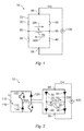
- a conventional commutation circuit 10 comprises an H bridge 20 with four main switches 30, 40, 50, 60.
- a coil 70 in which the current direction is to be reversed is connected between a first output terminal 80 and a second output terminal 85 of the H bridge 20.
- a first input terminal 90 and a second input terminal 95 of the H bridge 20 are connected to a current source 100 which provides a constant cell current I DC .
- the four main switches are operated appropriately to make the coil current I L flow in a desired direction in the coil. For example, according to figure 1 a first main switch 30 and a second main switch 40 are closed, and the coil current I L flows from left to right in the figure (positive direction 290). In order to reverse the coil current I L to flow from right to left (negative direction 300), a third main switch 50 and a fourth main switch 60 are closed, and the first and the second main switches 30, 40 are opened.
- the main switches are typically realized as semiconductor devices. Since the commutation circuit topology of figure 1 requires that all the main switches can be actively opened, the respective semiconductor devices need to be of turn-off type i.e. of a type that can be actively turned off. In addition, the semiconductor devices need to have a reverse blocking capability. Examples of such semiconductor devices are symmetrical GTOs and reverse blocking IGBTs.
- thyristors are not turn-off type semiconductor devices. Therefore, thyristors would not work as main switches in the topology according to figure 1 since a thyristor is only turned off when current through it becomes zero or close to zero. However, thyristors have low losses and they are cheap in comparison with the turn-off type semiconductor devices. It would therefore be desirable to enable the use of thyristors as main switches in an H bridge of a commutation circuit.
- WO2012/062376 discloses a commutation circuit for reversing a coil current in a coil of an electrical machine.
- the commutation circuit comprises a capacitor arranged to form a resonant circuit with the coil.
- the main switches in the H bridges disclosed in WO2012/062376 need to be of turn-off type in order for the commutation to work as described.
- One object of the invention is to provide a commutation circuit which enables the use of thyristors as main switches in an H bridge.
- a further object of the invention is to provide a commutation circuit with low losses irrespective of what kind of switches are used as main switches in the H bridge.
- the invention is based on the realization that by generating an appropriate bypass current with help of a voltage source, a switch current through a desired main switch in a leading state can be decreased and eventually brought to zero.
- Zero switch current in its turn enables the use of thyristors as main switches as it results in the thyristors to be turned off automatically.
- decreased switch current at the switching moment reduces switching losses even in different types of switches such as GTOs and IGBTs.
- a commutation circuit comprising a coil connected to an H bridge, the H bridge comprising four main switches for reversing polarity and a resulting coil current in the coil.
- the commutation circuit further comprises a voltage source configured to generate a bypass current, and at least one auxiliary switch for controlling the bypass current to thereby decrease a switch current through at least one of the main switches.
- the voltage source is configured to generate a bypass current to thereby bring the switch current to zero.
- Zero switch current results in thyristors to be turned off automatically in a reliable way.
- the voltage source comprises a capacitor.
- a capacitor By means of a capacitor the required voltage can be provided in a simple way.
- the coil current at least partially results from a cell current generated by a current source, and the cell current is furthermore used to pre-charge the capacitor.
- the cell current is used to pre-charge the capacitor no additional pre-charge circuit is needed.
- At least one of the main switches comprises a thyristor.
- a thyristor is a preferred main switch type in a commutation circuit as thyristors are simple, cheap, and have low losses.
- all the main switches are thyristors.
- all the auxiliary switches are thyristors.
- the voltage source is connected in parallel with at least one of the main switches.
- the voltage source is connected in series with the coil.
- an electrical machine comprises a commutation circuit according to any of the embodiments disclosed hereinbefore.
- a method for reversing a current direction in a coil comprising the steps of: providing a coil connected to an H bridge, the H bridge comprising four main switches; and generating a bypass current and controlling it to thereby decrease a switch current through at least one of the main switches.
- All embodiments of the invention disclosed herein comprise a sub-circuit corresponding to that shown in figure 1 , the only difference being that at least some of the main switches 30, 40, 50, 60 according to the disclosed embodiments of the invention are realized as thyristors.
- the sub-circuit comprising an H bridge 20 with four main switches 30, 40, 50, 60, a coil 70 connected to output terminals 80, 85 of the H bridge 20 and a current source 100 connected to input terminals 90, 95 of the H bridge 20 will be termed as a "cell".
- a commutation circuit 10 in addition to the cell comprising four main switches 30, 40, 50, 60 in the form of thyristors, comprises a voltage source in the form of a capacitor 110 connected in parallel with the H bridge 20 via a first diode 120 and a second diode 130.
- the capacitor 110 has a first terminal 115 and a second terminal 116.
- the capacitor 110 can furthermore be connected anti-parallel with the H bridge 20 by turning on a first auxiliary switch 140 and a second auxiliary switch 150.
- the first and second auxiliary switches 140, 150 are IGBTs each provided with an anti-parallel diode.
- the cell current I DC flows through the first main switch 30, the coil 70 and the second main switch 40, the coil current I L in the coil 70 flowing in a positive direction 290 and being equal with the cell current I DC .
- the capacitor 110 has been charged via the first diode 120 to have a positive polarity on the first terminal 115.
- the objective of the commutation is to reverse the coil current I L to flow through the third and fourth main switches 50, 60 and in a negative direction 300 in the coil 70.
- the first and second auxiliary switches 140, 150 are turned on, and the capacitor 110 is thereby connected anti-parallel with the H bridge 20.
- a capacitor current I C starts to increase, and the coil current I L starts to decrease.
- the capacitor 110 shall be dimensioned large enough to bring the coil current I L to zero, and when this occurs the first and second main switches 30, 40 are turned off automatically as their switch currents (a current through a switch) becomes zero.
- the first and second auxiliary switches 140, 150 are turned off, and the first input terminal 90 is thereby again brought into contact with the first terminal 115 via the diode 120, while the output terminal 95 is brought into contact with the second terminal 116 via the diode 130.
- the capacitor 110 starts to recharge positive polarity on the first terminal 115, and the third and fourth main switches 50, 60 are turned on.
- the turning on of the third and fourth main switches 50, 60 can be delayed in order to control the amount of energy on the capacitor 110 at the end of the commutation.
- the recharging of the capacitor 110 continues after the turning on of the third and fourth main switches 50, 60, and eventually the energy stored on the capacitor 110 becomes sufficient for the next commutation.
- the voltage source in the form of a capacitor 110 is connected either between the first output terminal 80 and the second input terminal 95 or between the second output terminal 85 and the second input terminal 95, depending on the states of a third auxiliary switch 160, a fourth auxiliary switch 170, a fifth auxiliary switch 180 and a sixth auxiliary switch 190. All the main switches 30, 40, 50, 60 and the auxiliary switches 160, 170, 180, 190 are thyristors.
- the coil current I L flows in a positive direction 290 and is equal with the cell current I DC .
- the capacitor 110 is pre-charged by means of a pre-charge circuit 200 to have a positive polarity on the first terminal 115.
- the objective of the commutation is to reverse the coil current I L to flow in a negative direction 300.
- the third main switch 50 and the third auxiliary switch 160 are turned on.
- the first main switch 30 is automatically turned off as a negative voltage is applied over it and the switch current is brought to zero, and the cell is short circuited through the third and second main switches 50, 40.
- the capacitor 110 now forms a resonance circuit together with the coil 70, and due to the pre-charge of the capacitor 110 the coil current I L slightly increases before decreasing to zero as the voltage over the capacitor 110 changes polarity and eventually stores all the energy of the resonance circuit.
- the fourth auxiliary switch 170 is turned on to allow the resonance to continue, and the coil current I L starts to increase in the negative direction 300 and eventually becomes equal with the cell current I DC .
- the second main switch 40 is automatically turned off, and as soon as the voltage over the capacitor 110 changes polarity the fourth main switch 60 is turned on.
- the objective of the commutation is now reached, and the capacitor 110 needs to be pre-charged with the same polarity as initially before a next commutation can be carried out.
- the commutation just described was carried out by connecting the capacitor 110 between the first output terminal 80 and the second input terminal 95.
- a next commutation is carried out in a corresponding manner, the only difference being that the capacitor 110 is now connected between the second output terminal 85 and the second input terminal 95 by appropriately operating the fifth and sixth auxiliary switches 180, 190.
- the commutation circuit 10 comprises a voltage source in the form of a combination of a first capacitor 110 and a second capacitor 111.
- the first capacitor 110 is pre-charged using the cell current I DC (for example by turning on a tenth auxiliary switch 240 and the second main switch 40) to have a positive polarity on a first terminal 115 and a negative one on a second terminal 116.
- the second capacitor 111 comprises a third terminal 117 and a fourth terminal 118, and it is not pre-charged.
- the first capacitor 110 needs to be dimensioned to contain sufficient amount of energy to turn off a single thyristor while the second capacitor 111 needs to be dimensioned to store somewhat more energy than the coil 70 at cell current I DC .
- the first capacitor 110 is therefore typically much smaller than the second capacitor 111.
- the commutation circuit 10 of figure 4 further comprises a seventh auxiliary switch 210, an eighth auxiliary switch 220 and a ninth auxiliary switch 230. All the main switches 30, 40, 50, 60 and the auxiliary switches 210, 220, 230, 240 are thyristors.
- the coil current I L flows in a positive direction 290 and is equal with the cell current I DC .
- the objective of a first commutation is to reverse the coil current I L to flow in a negative direction 300.
- the seventh auxiliary switch 210 is turned on.
- the positively pre-charged first terminal 115 is brought into contact with the second input terminal 95, and the second main switch 40 is automatically turned off as a negative voltage is applied over it and the switch current is brought to zero.
- the discharge of the first capacitor 110 continues until it changes polarity, at which instant the eighth auxiliary switch 220 is turned on.
- the cell current I DC continues to charge the first and the second capacitors 110, 111 in parallel. The duration of this charging can be controlled such that an appropriate amount of energy is available in the first capacitor 110 for completing the commutation.
- the fourth main switch 60 is turned on, and resonance between the coil 70 and the first and second capacitors 110, 111 begins.
- the coil current I L decreases to zero as the first and second capacitors 110, 111 eventually store all the energy of the resonance circuit, and the seventh and eighth auxiliary switches 210, 220 turn off automatically.
- the fourth terminal 118 and the second terminal 116 both retain a positive polarity at the end of this process, which polarity of the second terminal 116 will be utilized during a subsequent second commutation.
- the ninth auxiliary switch 230 is turned on, and the coil current I L starts to increase in the negative direction 300 and eventually becomes equal with the cell current I DC .
- the first main switch 30 is automatically turned off, and the cell current I DC continues to charge the second capacitor 111 with a positive polarity on the third terminal 117.
- the third main switch 50 is turned on, which results in the ninth auxiliary switch 230 being automatically turned off. The objective of the first commutation is now reached, and the second commutation can be carried out when desired.
- the voltage stored in the first capacitor 110 has a positive polarity on the second terminal 116, while the voltage stored in the second capacitor 111 is close to zero.
- the objective of the second commutation is to reverse the coil current I L again to flow in the positive direction 290.
- the tenth auxiliary switch 240 is turned on.
- the positive polarity on the second terminal 116 applies a negative voltage over the third main switch 50 which automatically turns off as the switch current is brought to zero.
- the discharge of the first capacitor 110 continues until it changes polarity, at which instant the ninth auxiliary switch 230 is turned on causing the cell current I DC to charge the first and second capacitors 110, 111 in parallel.
- the duration of this charging can be controlled such that an appropriate amount of energy is available in the first capacitor 110 for completing the commutation.
- the first main switch 30 is turned on, and the first and second capacitors 110, 111 now form a resonance circuit together with the coil 70.
- the ninth and tenth auxiliary switches 230, 240 turn off automatically as the coil current I L reaches zero.
- the first capacitor 110 is thereby left with a positive polarity on the first terminal 115, and the second capacitor 111 with a positive polarity on the third terminal 117.
- the cell at this phase is short circuited through the first and fourth main switches 30, 60, and the coil current I L is zero.
- the eighth auxiliary switch 220 is turned on.
- the coil current I L starts to increase in the positive direction 290 and eventually becomes equal with the cell current I DC .
- the fourth main switch 60 is automatically turned off, and as soon as the voltage over the second capacitor 111 changes polarity the second main switch 40 is turned on. This causes the eighth auxiliary switch 220 to be automatically turned off.
- the objective of the second commutation is now reached, and a next commutation can be carried out when desired as the first capacitor 110 is already pre-charged with the same polarity as initially.
- a great advantage of the embodiment according to figure 4 in comparison with that of figure 3 is that a separate pre-charge circuit 200 is not needed. Instead, the commutation circuit 10 of figure 4 utilizes the cell current I DC for pre-charging the first and second capacitors 110, 111.
- the commutation circuit 10 comprises a voltage source in the form of a capacitor 110 connected either between the second output terminal 85 and the second input terminal 95 or between the second output terminal 85 and the first input terminal 90, depending on the states of an eleventh auxiliary switch 250 and a twelfth auxiliary switch 260. All the main switches 30, 40, 50, 60 and both auxiliary switches 250, 260 are thyristors.
- the coil current I L flows in a positive direction 290 and is equal with the cell current I DC .
- the capacitor 110 is pre-charged by means of a pre-charge circuit 200 to have a positive polarity on the first terminal 115.
- the pre-charge energy needs to be just enough to turn off a single thyristor. Because according to the embodiment of figure 5 the capacitor 110 needs to be dimensioned to store somewhat more energy than the coil 70 at cell current I DC , the pre-charged energy is only a fraction of the capacitor's 110 capacitance.
- the objective of the commutation is to reverse the coil current I L to flow in a negative direction 300.
- the eleventh auxiliary switch 250 is turned on.
- the second main switch 40 is automatically turned off as a negative voltage is applied over it and the switch current is brought to zero, and the coil current I L starts charging the capacitor 110 with a positive polarity on the second terminal 116.
- This charging of the capacitor 110 is allowed to continue to store a desired amount of energy in the capacitor 110.
- the fourth main switch 60 is turned on, and the cell is thus short circuited through the first and fourth main switches 30, 60.
- the capacitor 110 now forms a resonance circuit together with the coil 70, and the coil current I L decreases to zero as the capacitor 110 eventually stores all the energy of the resonance circuit.
- the eleventh auxiliary switch 250 is automatically turned off.
- the capacitor 110 should contain enough energy to carry through the following phases of the commutation i.e. somewhat more than the energy of the coil 70 at cell current I DC .
- the twelfth auxiliary switch 260 is turned on, and a resonance circuit between the capacitor 110 and the coil 70 is again formed.
- the coil current I L starts to increase in the negative direction 300 and eventually becomes equal with the cell current I DC .
- the first main switch 30 is automatically turned off, and as soon as the voltage over the capacitor 110 changes polarity the third main switch 50 is turned on and the twelfth auxiliary switch 260 is automatically turned off.
- the objective of the commutation is now reached, and a next commutation can be carried out in a corresponding manner as the commutation just described.
- the capacitor 110 needs to be pre-charged with an opposite polarity than initially before the next commutation can be carried out, and the next commutation is initiated by turning on the twelfth auxiliary switch 260.
- the commutation circuit 10 comprises a voltage source in the form of a capacitor 110 connected in series with the coil 70.
- a thirteenth auxiliary switch 270 and a fourteenth auxiliary switch 280 are connected in parallel with the capacitor 110, the two auxiliary switches 270, 280 being anti-parallel in relation to each other.
- the first and third main switches 30, 50 and both auxiliary switches 270, 280 are GTOs, and the second and fourth main switches 40, 60 are thyristors.
- the coil current I L flows in a positive direction 290 and is equal with the cell current I DC .
- the thirteenth auxiliary switch 270 is turned on and the capacitor 110 is thus bypassed and has a zero voltage.
- the objective of the commutation is to reverse the coil current I L to flow in a negative direction 300.
- the thirteenth auxiliary switch 270 is turned off, and the fourth main switch 60 is simultaneously turned on.
- the cell is short circuited through the first and fourth main switches 30, 60.
- the capacitor 110 now forms a resonance circuit together with the coil 70, and the coil current I L decreases to zero as the capacitor 110 eventually stores all the energy of the resonance circuit. As this occurs the second main switch 40 is automatically turned off.
- the third main switch 50 is turned on, and a resonance circuit between the capacitor 110 and the coil 70 is again formed.
- the coil current I L starts to increase in the negative direction 300 and eventually becomes close to equal with the cell current I DC .
- the coil current I L in the negative direction 300 could indeed become equal with the cell current I DC
- the coil current I L in the negative direction 300 could become high enough to automatically turn off the first main switch 30 should it be a thyristor.
- the first main switch 30 is a GTO, and it is actively turned off as soon as the voltage over the capacitor 110 changes polarity and the switch current through the first main switch 30 becomes close to zero.
- the fourteenth auxiliary switch 280 is turned on simultaneously with the turning off of the first main switch 30. This will bypass the capacitor 110 now that the coil current I L flows in the negative direction 300.
- the objective of the commutation is now reached, and the commutation circuit 10 is at a state that is identical with the initial state except the fact that the coil current I L flows in the negative direction 300.
- a next commutation can now be carried out in a corresponding manner as the commutation just described.
- FIG. 6 an alternative mode of operating the commutation circuit 10 is suggested.
- the thirteenth auxiliary switch 270 is turned off first.
- the cell current I DC will now charge the capacitor 110 with extra energy which can be utilized later for compensating losses within the circuit.
- the fourth main switch 60 is turned on and the following commutation phases occur as described hereinbefore.
- the advantage of charging the capacitor 110 with extra energy is that the capacitor 110 now contains enough energy to increase the coil current I L to be equal with the cell current I DC .
- the first main switch 30 in the form of a GTO can be replaced with a thyristor and the commutation will still succeed.
- the commutation circuits 10 described herein can be utilized in controlling coil currents I L in coils of an electrical machine, such as a transformer, an electrical motor or a generator.
- an electrical machine such as a transformer, an electrical motor or a generator.
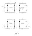
- FIG. 7 shows four positions to which the voltage source (here in the form of a capacitor 110) can be connected in relation to the H bridge 20 at different phases of the commutation.
- the current source 100 may be replaced with any suitable source that generates current to the coil 70, such as a voltage source in series with an inductance. Such source shall in the context of the present invention be considered as a current source 100.
- any current generated by a voltage source shall be considered as a bypass current if it results in a decrease of a switch current through at least one of the main switches 30, 40, 50, 60, even if the respective current not necessarily bypasses the respective switch.
Landscapes
- Engineering & Computer Science (AREA)
- Power Engineering (AREA)
- Inverter Devices (AREA)
- Driving Mechanisms And Operating Circuits Of Arc-Extinguishing High-Tension Switches (AREA)
Abstract
A commutation circuit (10) comprises a coil (70) connected to an H bridge (20), the H bridge (20) comprising four main switches (30, 40, 50, 60) for reversing polarity and a resulting coil current (IL) in the coil (70). The commutation circuit (10) further comprises a voltage source (110, 111) configured to generate a bypass current, and at least one auxiliary switch (140, 150, 160, 170, 180, 190, 210, 220, 230, 240, 250, 260, 270, 280) for controlling the bypass current to thereby decrease a switch current through at least one of the main switches (30, 40, 50, 60). By generating an appropriate bypass current with help of a voltage source (110, 111), a switch current through a desired main switch (30, 40, 50, 60) in a leading state can be decreased and eventually brought to zero. Zero current in its turn enables the use of thyristors as main switches (30, 40, 50, 60) as it results in the thyristors to be turned off automatically. Furthermore, decreased switch current at the switching moment reduces switching losses even in different types of switches such as GTOs and IGBTs.
Description
- The present invention relates to a circuit for consecutively reversing a current direction in a coil.
- Referring to
figure 1 , aconventional commutation circuit 10 comprises anH bridge 20 with fourmain switches coil 70 in which the current direction is to be reversed is connected between afirst output terminal 80 and asecond output terminal 85 of theH bridge 20. Afirst input terminal 90 and asecond input terminal 95 of theH bridge 20 are connected to acurrent source 100 which provides a constant cell current IDC. The four main switches are operated appropriately to make the coil current IL flow in a desired direction in the coil. For example, according tofigure 1 a firstmain switch 30 and a secondmain switch 40 are closed, and the coil current IL flows from left to right in the figure (positive direction 290). In order to reverse the coil current IL to flow from right to left (negative direction 300), a thirdmain switch 50 and a fourthmain switch 60 are closed, and the first and the secondmain switches - The main switches are typically realized as semiconductor devices. Since the commutation circuit topology of
figure 1 requires that all the main switches can be actively opened, the respective semiconductor devices need to be of turn-off type i.e. of a type that can be actively turned off. In addition, the semiconductor devices need to have a reverse blocking capability. Examples of such semiconductor devices are symmetrical GTOs and reverse blocking IGBTs. On the other hand, thyristors are not turn-off type semiconductor devices. Therefore, thyristors would not work as main switches in the topology according tofigure 1 since a thyristor is only turned off when current through it becomes zero or close to zero. However, thyristors have low losses and they are cheap in comparison with the turn-off type semiconductor devices. It would therefore be desirable to enable the use of thyristors as main switches in an H bridge of a commutation circuit. -
WO2012/062376 discloses a commutation circuit for reversing a coil current in a coil of an electrical machine. The commutation circuit comprises a capacitor arranged to form a resonant circuit with the coil. The main switches in the H bridges disclosed inWO2012/062376 need to be of turn-off type in order for the commutation to work as described. - One object of the invention is to provide a commutation circuit which enables the use of thyristors as main switches in an H bridge. A further object of the invention is to provide a commutation circuit with low losses irrespective of what kind of switches are used as main switches in the H bridge.
- These objects are achieved by the device according to appended claim 1 and the method according to appended claim 11.
- The invention is based on the realization that by generating an appropriate bypass current with help of a voltage source, a switch current through a desired main switch in a leading state can be decreased and eventually brought to zero. Zero switch current in its turn enables the use of thyristors as main switches as it results in the thyristors to be turned off automatically. Furthermore, decreased switch current at the switching moment reduces switching losses even in different types of switches such as GTOs and IGBTs.
- According to a first aspect of the invention, there is provided a commutation circuit comprising a coil connected to an H bridge, the H bridge comprising four main switches for reversing polarity and a resulting coil current in the coil. The commutation circuit further comprises a voltage source configured to generate a bypass current, and at least one auxiliary switch for controlling the bypass current to thereby decrease a switch current through at least one of the main switches. The ability to controllably decrease switch currents through the main switches reduces switching losses, and provided that the switch currents are reduces sufficiently also enables the use of thyristors as main switches.
- According to one embodiment of the invention, the voltage source is configured to generate a bypass current to thereby bring the switch current to zero. Zero switch current results in thyristors to be turned off automatically in a reliable way.
- According to one embodiment of the invention, the voltage source comprises a capacitor. By means of a capacitor the required voltage can be provided in a simple way.
- According to one embodiment of the invention, the coil current at least partially results from a cell current generated by a current source, and the cell current is furthermore used to pre-charge the capacitor. When the cell current is used to pre-charge the capacitor no additional pre-charge circuit is needed.
- According to one embodiment of the invention, at least one of the main switches comprises a thyristor. A thyristor is a preferred main switch type in a commutation circuit as thyristors are simple, cheap, and have low losses.
- According to one embodiment of the invention, all the main switches are thyristors.
- According to one embodiment of the invention, all the auxiliary switches are thyristors.
- According to one embodiment of the invention, the voltage source is connected in parallel with at least one of the main switches.
- According to one embodiment of the invention, the voltage source is connected in series with the coil.
- According to one embodiment of the invention, an electrical machine comprises a commutation circuit according to any of the embodiments disclosed hereinbefore.
- According to a second aspect of the invention, there is provided a method for reversing a current direction in a coil, the method comprising the steps of: providing a coil connected to an H bridge, the H bridge comprising four main switches; and generating a bypass current and controlling it to thereby decrease a switch current through at least one of the main switches.
- The invention will be explained in greater detail with reference to the accompanying drawings, wherein
- figure 1
- shows a conventional commutation circuit,
- figure 2
- shows a commutation circuit according to one embodiment of the invention,
- figure 3
- shows a commutation circuit according to one embodiment of the invention,
- figure 4
- shows a commutation circuit according to one embodiment of the invention,
- figure 5
- shows a commutation circuit according to one embodiment of the invention,
- figure 6
- shows a commutation circuit according to one embodiment of the invention, and
- figure 7
- shows four positions to which a voltage source can be connected in relation to an H bridge at different phases of a commutation.
- All embodiments of the invention disclosed herein comprise a sub-circuit corresponding to that shown in
figure 1 , the only difference being that at least some of themain switches H bridge 20 with fourmain switches coil 70 connected tooutput terminals H bridge 20 and acurrent source 100 connected toinput terminals H bridge 20 will be termed as a "cell". - Referring to
figure 2 , in addition to the cell comprising fourmain switches commutation circuit 10 according to one embodiment of the invention comprises a voltage source in the form of acapacitor 110 connected in parallel with theH bridge 20 via afirst diode 120 and asecond diode 130. Thecapacitor 110 has afirst terminal 115 and asecond terminal 116. Thecapacitor 110 can furthermore be connected anti-parallel with theH bridge 20 by turning on a firstauxiliary switch 140 and a secondauxiliary switch 150. According to the embodiment offigure 2 the first and secondauxiliary switches - At an initial state of the
commutation circuit 10 the cell current IDC flows through the firstmain switch 30, thecoil 70 and the secondmain switch 40, the coil current IL in thecoil 70 flowing in apositive direction 290 and being equal with the cell current IDC. Thecapacitor 110 has been charged via thefirst diode 120 to have a positive polarity on thefirst terminal 115. The objective of the commutation is to reverse the coil current IL to flow through the third and fourthmain switches negative direction 300 in thecoil 70. At a first phase of the commutation the first and secondauxiliary switches capacitor 110 is thereby connected anti-parallel with theH bridge 20. As a consequence, a capacitor current IC starts to increase, and the coil current IL starts to decrease. Thecapacitor 110 shall be dimensioned large enough to bring the coil current IL to zero, and when this occurs the first and secondmain switches - At a second phase of the commutation the first and second
auxiliary switches first input terminal 90 is thereby again brought into contact with thefirst terminal 115 via thediode 120, while theoutput terminal 95 is brought into contact with thesecond terminal 116 via thediode 130. Thecapacitor 110 starts to recharge positive polarity on thefirst terminal 115, and the third and fourthmain switches main switches capacitor 110 at the end of the commutation. The recharging of thecapacitor 110 continues after the turning on of the third and fourthmain switches capacitor 110 becomes sufficient for the next commutation. The objective of the commutation is now reached, and thecommutation circuit 10 is at a state that is identical with the initial state except the fact that the coil current IL flows in thenegative direction 300. A next commutation can now be carried out in a corresponding manner as the commutation just described. - Referring to
figure 3 , according to one embodiment of the invention the voltage source in the form of acapacitor 110 is connected either between thefirst output terminal 80 and thesecond input terminal 95 or between thesecond output terminal 85 and thesecond input terminal 95, depending on the states of a thirdauxiliary switch 160, a fourthauxiliary switch 170, a fifthauxiliary switch 180 and a sixthauxiliary switch 190. All themain switches auxiliary switches - At an initial state of the
commutation circuit 10 the coil current IL flows in apositive direction 290 and is equal with the cell current IDC. Thecapacitor 110 is pre-charged by means of apre-charge circuit 200 to have a positive polarity on thefirst terminal 115. The objective of the commutation is to reverse the coil current IL to flow in anegative direction 300. At a first phase of the commutation the thirdmain switch 50 and the thirdauxiliary switch 160 are turned on. As a consequence, the firstmain switch 30 is automatically turned off as a negative voltage is applied over it and the switch current is brought to zero, and the cell is short circuited through the third and secondmain switches - The
capacitor 110 now forms a resonance circuit together with thecoil 70, and due to the pre-charge of thecapacitor 110 the coil current IL slightly increases before decreasing to zero as the voltage over thecapacitor 110 changes polarity and eventually stores all the energy of the resonance circuit. The fourthauxiliary switch 170 is turned on to allow the resonance to continue, and the coil current IL starts to increase in thenegative direction 300 and eventually becomes equal with the cell current IDC. As this occurs the secondmain switch 40 is automatically turned off, and as soon as the voltage over thecapacitor 110 changes polarity the fourthmain switch 60 is turned on. - The objective of the commutation is now reached, and the
capacitor 110 needs to be pre-charged with the same polarity as initially before a next commutation can be carried out. The commutation just described was carried out by connecting thecapacitor 110 between thefirst output terminal 80 and thesecond input terminal 95. A next commutation is carried out in a corresponding manner, the only difference being that thecapacitor 110 is now connected between thesecond output terminal 85 and thesecond input terminal 95 by appropriately operating the fifth and sixthauxiliary switches - Referring to
figure 4 , according to one embodiment of the invention thecommutation circuit 10 comprises a voltage source in the form of a combination of afirst capacitor 110 and asecond capacitor 111. Thefirst capacitor 110 is pre-charged using the cell current IDC (for example by turning on a tenthauxiliary switch 240 and the second main switch 40) to have a positive polarity on afirst terminal 115 and a negative one on asecond terminal 116. Thesecond capacitor 111 comprises athird terminal 117 and afourth terminal 118, and it is not pre-charged. Thefirst capacitor 110 needs to be dimensioned to contain sufficient amount of energy to turn off a single thyristor while thesecond capacitor 111 needs to be dimensioned to store somewhat more energy than thecoil 70 at cell current IDC. Thefirst capacitor 110 is therefore typically much smaller than thesecond capacitor 111. Thecommutation circuit 10 offigure 4 further comprises a seventhauxiliary switch 210, an eighthauxiliary switch 220 and a ninthauxiliary switch 230. All themain switches auxiliary switches - At an initial state of the
commutation circuit 10 the coil current IL flows in apositive direction 290 and is equal with the cell current IDC. The objective of a first commutation is to reverse the coil current IL to flow in anegative direction 300. At a first phase of the first commutation the seventhauxiliary switch 210 is turned on. As a consequence, the positively pre-chargedfirst terminal 115 is brought into contact with thesecond input terminal 95, and the secondmain switch 40 is automatically turned off as a negative voltage is applied over it and the switch current is brought to zero. The discharge of thefirst capacitor 110 continues until it changes polarity, at which instant the eighthauxiliary switch 220 is turned on. The cell current IDC continues to charge the first and thesecond capacitors first capacitor 110 for completing the commutation. - At a second phase of the first commutation the fourth
main switch 60 is turned on, and resonance between thecoil 70 and the first andsecond capacitors second capacitors auxiliary switches fourth terminal 118 and thesecond terminal 116 both retain a positive polarity at the end of this process, which polarity of thesecond terminal 116 will be utilized during a subsequent second commutation. - At a third phase of the first commutation the ninth
auxiliary switch 230 is turned on, and the coil current IL starts to increase in thenegative direction 300 and eventually becomes equal with the cell current IDC. As this occurs the firstmain switch 30 is automatically turned off, and the cell current IDC continues to charge thesecond capacitor 111 with a positive polarity on thethird terminal 117. As soon as the voltage over thesecond capacitor 111 changes polarity the thirdmain switch 50 is turned on, which results in the ninthauxiliary switch 230 being automatically turned off. The objective of the first commutation is now reached, and the second commutation can be carried out when desired. The voltage stored in thefirst capacitor 110 has a positive polarity on thesecond terminal 116, while the voltage stored in thesecond capacitor 111 is close to zero. The objective of the second commutation is to reverse the coil current IL again to flow in thepositive direction 290. - At a first phase of the second commutation the tenth
auxiliary switch 240 is turned on. The positive polarity on thesecond terminal 116 applies a negative voltage over the thirdmain switch 50 which automatically turns off as the switch current is brought to zero. The discharge of thefirst capacitor 110 continues until it changes polarity, at which instant the ninthauxiliary switch 230 is turned on causing the cell current IDC to charge the first andsecond capacitors first capacitor 110 for completing the commutation. - At a second phase of the second commutation the first
main switch 30 is turned on, and the first andsecond capacitors coil 70. The ninth and tenthauxiliary switches first capacitor 110 is thereby left with a positive polarity on thefirst terminal 115, and thesecond capacitor 111 with a positive polarity on thethird terminal 117. The cell at this phase is short circuited through the first and fourthmain switches - At a third phase of the second commutation the eighth
auxiliary switch 220 is turned on. The coil current IL starts to increase in thepositive direction 290 and eventually becomes equal with the cell current IDC. As this occurs the fourthmain switch 60 is automatically turned off, and as soon as the voltage over thesecond capacitor 111 changes polarity the secondmain switch 40 is turned on. This causes the eighthauxiliary switch 220 to be automatically turned off. The objective of the second commutation is now reached, and a next commutation can be carried out when desired as thefirst capacitor 110 is already pre-charged with the same polarity as initially. - A great advantage of the embodiment according to
figure 4 in comparison with that offigure 3 is that a separatepre-charge circuit 200 is not needed. Instead, thecommutation circuit 10 offigure 4 utilizes the cell current IDC for pre-charging the first andsecond capacitors - Referring to
figure 5 , according to one embodiment of the invention thecommutation circuit 10 comprises a voltage source in the form of acapacitor 110 connected either between thesecond output terminal 85 and thesecond input terminal 95 or between thesecond output terminal 85 and thefirst input terminal 90, depending on the states of an eleventhauxiliary switch 250 and a twelfthauxiliary switch 260. All themain switches auxiliary switches - At an initial state of the
commutation circuit 10 the coil current IL flows in apositive direction 290 and is equal with the cell current IDC. Thecapacitor 110 is pre-charged by means of apre-charge circuit 200 to have a positive polarity on thefirst terminal 115. The pre-charge energy needs to be just enough to turn off a single thyristor. Because according to the embodiment offigure 5 thecapacitor 110 needs to be dimensioned to store somewhat more energy than thecoil 70 at cell current IDC, the pre-charged energy is only a fraction of the capacitor's 110 capacitance. The objective of the commutation is to reverse the coil current IL to flow in anegative direction 300. - At a first phase of the commutation the eleventh
auxiliary switch 250 is turned on. As a consequence, the secondmain switch 40 is automatically turned off as a negative voltage is applied over it and the switch current is brought to zero, and the coil current IL starts charging thecapacitor 110 with a positive polarity on thesecond terminal 116. This charging of thecapacitor 110 is allowed to continue to store a desired amount of energy in thecapacitor 110. At a second phase of the commutation the fourthmain switch 60 is turned on, and the cell is thus short circuited through the first and fourthmain switches capacitor 110 now forms a resonance circuit together with thecoil 70, and the coil current IL decreases to zero as thecapacitor 110 eventually stores all the energy of the resonance circuit. As this occurs the eleventhauxiliary switch 250 is automatically turned off. At this moment thecapacitor 110 should contain enough energy to carry through the following phases of the commutation i.e. somewhat more than the energy of thecoil 70 at cell current IDC. - At a third phase of the commutation the twelfth
auxiliary switch 260 is turned on, and a resonance circuit between thecapacitor 110 and thecoil 70 is again formed. The coil current IL starts to increase in thenegative direction 300 and eventually becomes equal with the cell current IDC. As this occurs the firstmain switch 30 is automatically turned off, and as soon as the voltage over thecapacitor 110 changes polarity the thirdmain switch 50 is turned on and the twelfthauxiliary switch 260 is automatically turned off. The objective of the commutation is now reached, and a next commutation can be carried out in a corresponding manner as the commutation just described. Thecapacitor 110 needs to be pre-charged with an opposite polarity than initially before the next commutation can be carried out, and the next commutation is initiated by turning on the twelfthauxiliary switch 260. - Referring to
figure 6 , according to one embodiment of the invention thecommutation circuit 10 comprises a voltage source in the form of acapacitor 110 connected in series with thecoil 70. A thirteenthauxiliary switch 270 and a fourteenthauxiliary switch 280 are connected in parallel with thecapacitor 110, the twoauxiliary switches main switches auxiliary switches main switches - At an initial state of the
commutation circuit 10 the coil current IL flows in apositive direction 290 and is equal with the cell current IDC. The thirteenthauxiliary switch 270 is turned on and thecapacitor 110 is thus bypassed and has a zero voltage. The objective of the commutation is to reverse the coil current IL to flow in anegative direction 300. - At a first phase of the commutation the thirteenth
auxiliary switch 270 is turned off, and the fourthmain switch 60 is simultaneously turned on. As a consequence, the cell is short circuited through the first and fourthmain switches capacitor 110 now forms a resonance circuit together with thecoil 70, and the coil current IL decreases to zero as thecapacitor 110 eventually stores all the energy of the resonance circuit. As this occurs the secondmain switch 40 is automatically turned off. - At a second phase of the commutation the third
main switch 50 is turned on, and a resonance circuit between thecapacitor 110 and thecoil 70 is again formed. The coil current IL starts to increase in thenegative direction 300 and eventually becomes close to equal with the cell current IDC. In a lossless circuit the coil current IL in thenegative direction 300 could indeed become equal with the cell current IDC, and in a circuit with low losses the coil current IL in thenegative direction 300 could become high enough to automatically turn off the firstmain switch 30 should it be a thyristor. However, according to the embodiment offigure 6 the firstmain switch 30 is a GTO, and it is actively turned off as soon as the voltage over thecapacitor 110 changes polarity and the switch current through the firstmain switch 30 becomes close to zero. - At a third phase of the commutation the fourteenth
auxiliary switch 280 is turned on simultaneously with the turning off of the firstmain switch 30. This will bypass thecapacitor 110 now that the coil current IL flows in thenegative direction 300. The objective of the commutation is now reached, and thecommutation circuit 10 is at a state that is identical with the initial state except the fact that the coil current IL flows in thenegative direction 300. A next commutation can now be carried out in a corresponding manner as the commutation just described. - Further referring to
figure 6 , an alternative mode of operating thecommutation circuit 10 is suggested. Instead of simultaneously turning off the thirteenthauxiliary switch 270 and turning on the fourthmain switch 60 at the first phase of the commutation, the thirteenthauxiliary switch 270 is turned off first. The cell current IDC will now charge thecapacitor 110 with extra energy which can be utilized later for compensating losses within the circuit. After an appropriate delay the fourthmain switch 60 is turned on and the following commutation phases occur as described hereinbefore. The advantage of charging thecapacitor 110 with extra energy is that thecapacitor 110 now contains enough energy to increase the coil current IL to be equal with the cell current IDC. Consequently, the firstmain switch 30 in the form of a GTO can be replaced with a thyristor and the commutation will still succeed. The same applies to the thirdmain switch 50 when a corresponding delay is introduced when turning on the secondmain switch 40 during commutation in an opposite direction. - The
commutation circuits 10 described herein can be utilized in controlling coil currents IL in coils of an electrical machine, such as a transformer, an electrical motor or a generator. In such applications the voltage generated by an electromotive force (emf) between the first andsecond output terminals H bridge 20, as well as losses (electrical energy transformed into heat or mechanical energy), shall be taken into consideration when dimensioning the components and when operating therespective commutation circuit 10. - The invention is not limited to the embodiments shown above, but the person skilled in the art may modify them in a plurality of ways within the scope of the invention as defined by the claims. Thus, numerous other topologies than those disclosed above can be utilized to achieve the technical effect of the invention i.e. to decrease a switch current through a desired
main switch Figure 7 shows four positions to which the voltage source (here in the form of a capacitor 110) can be connected in relation to theH bridge 20 at different phases of the commutation. Furthermore, thecurrent source 100 may be replaced with any suitable source that generates current to thecoil 70, such as a voltage source in series with an inductance. Such source shall in the context of the present invention be considered as acurrent source 100. - In order for the commutation to work as described when using the disclosed topologies it needs to be assumed that the capacitors, the switches, eventual pre-charge circuits and other components are appropriately dimensioned and that the switches are appropriately controlled. Instead of using capacitors as voltage sources according to the embodiments shown above any other suitable voltage sources can be used. Furthermore, any current generated by a voltage source shall be considered as a bypass current if it results in a decrease of a switch current through at least one of the
main switches main switch commutation circuits 10 where none of themain switches
Claims (14)
- A commutation circuit (10) comprising:a coil (70) connected to an H bridge (20), the H bridge (20) comprising four main switches (30, 40, 50, 60) for reversing polarity and a resulting coil current (IL) in the coil (70),characterized in that the commutation circuit (10) further comprises a voltage source (110, 111) configured to generate a bypass current, and at least one auxiliary switch (140, 150, 160, 170, 180, 190, 210, 220, 230, 240, 250, 260, 270, 280) for controlling the bypass current to thereby decrease a switch current through at least one of the main switches (30, 40, 50, 60).
- A commutation circuit (10) according to claim 1, wherein the voltage source (110, 111) is configured to generate a bypass current to thereby bring the switch current to zero.
- A commutation circuit (10) according to any of the preceding claims, wherein the voltage source comprises a capacitor (110, 111).
- A commutation circuit (10) according to claim 3, wherein the coil current (IL) at least partially results from a cell current (IDC) generated by a current source (100), and the cell current (IDC) is furthermore used to pre-charge the capacitor (110, 111).
- A commutation circuit (10) according to any of the preceding claims, wherein at least one of the main switches (30, 40, 50, 60) comprises a thyristor.
- A commutation circuit (10) according to any of the preceding claims, wherein all the main switches (30, 40, 50, 60) are thyristors.
- A commutation circuit (10) according to any of the preceding claims, wherein all the auxiliary switches (140, 150, 160, 170, 180, 190, 210, 220, 230, 240, 250, 260) are thyristors.
- A commutation circuit (10) according to any of the preceding claims, wherein the voltage source (110, 111) is connected in parallel with at least one of the main switches (30, 40, 50, 60).
- A commutation circuit (10) according to any of the preceding claims, wherein the voltage source (110, 111) is connected in series with the coil (70).
- An electrical machine comprising a commutation circuit (10) according to any of the preceding claims.
- A method for reversing a current direction in a coil (70), the method comprising the steps of:- providing a coil (70) connected to an H bridge (20), the H bridge (20) comprising four main switches (30, 40, 50, 60); and- generating a bypass current and controlling it to thereby decrease a switch current through at least one of the main switches (30, 40, 50, 60).
- A method according to claim 11, wherein the bypass current is configured to bring the switch current to zero.
- A method according to any of claims 11 to 12, wherein the bypass current is generated by means of a capacitor (110, 111).
- A method according to claim 13, wherein the method further comprises the steps of:- providing a current source (100) for feeding the coil (70) with a cell current (IDC) ; and- pre-charging the capacitor (110, 111) with the cell current (IDC) .
Priority Applications (5)
| Application Number | Priority Date | Filing Date | Title |
|---|---|---|---|
| EP14162538.4A EP2928066A1 (en) | 2014-03-31 | 2014-03-31 | A high efficiency commutation circuit |
| CN201580015225.7A CN106134067B (en) | 2014-03-31 | 2015-03-31 | High-efficiency reversing circuit |
| PCT/EP2015/056942 WO2015150349A1 (en) | 2014-03-31 | 2015-03-31 | A high efficiency commutation circuit |
| US15/122,854 US10840833B2 (en) | 2014-03-31 | 2015-03-31 | High efficiency commutation circuit |
| EP15713727.4A EP3127232A1 (en) | 2014-03-31 | 2015-03-31 | A high efficiency commutation circuit |
Applications Claiming Priority (1)
| Application Number | Priority Date | Filing Date | Title |
|---|---|---|---|
| EP14162538.4A EP2928066A1 (en) | 2014-03-31 | 2014-03-31 | A high efficiency commutation circuit |
Publications (1)
| Publication Number | Publication Date |
|---|---|
| EP2928066A1 true EP2928066A1 (en) | 2015-10-07 |
Family
ID=50391060
Family Applications (2)
| Application Number | Title | Priority Date | Filing Date |
|---|---|---|---|
| EP14162538.4A Withdrawn EP2928066A1 (en) | 2014-03-31 | 2014-03-31 | A high efficiency commutation circuit |
| EP15713727.4A Pending EP3127232A1 (en) | 2014-03-31 | 2015-03-31 | A high efficiency commutation circuit |
Family Applications After (1)
| Application Number | Title | Priority Date | Filing Date |
|---|---|---|---|
| EP15713727.4A Pending EP3127232A1 (en) | 2014-03-31 | 2015-03-31 | A high efficiency commutation circuit |
Country Status (4)
| Country | Link |
|---|---|
| US (1) | US10840833B2 (en) |
| EP (2) | EP2928066A1 (en) |
| CN (1) | CN106134067B (en) |
| WO (1) | WO2015150349A1 (en) |
Families Citing this family (2)
| Publication number | Priority date | Publication date | Assignee | Title |
|---|---|---|---|---|
| EP3327911B1 (en) * | 2016-11-23 | 2020-10-21 | Maschinenfabrik Reinhausen GmbH | Method for controlling a switch module based on thyristor switching elements |
| US20180285241A1 (en) * | 2017-03-28 | 2018-10-04 | Carnegie Mellon University | Energy-interference-free debugger for intermittent energy-harvesting systems |
Citations (8)
| Publication number | Priority date | Publication date | Assignee | Title |
|---|---|---|---|---|
| DE3130102A1 (en) * | 1980-09-29 | 1982-05-06 | VEB Elektromotorenwerk Hartha, DDR 7302 Hartha | Electronic off-commutation of the stator windings of electronically commutated motors |
| DE3725515A1 (en) * | 1987-07-29 | 1989-02-09 | Licentia Gmbh | Extinguishing thyristors of railway or industrial power converter - using self-commutating rectifier across AC voltage terminals of main rectifier |
| JPH1169876A (en) * | 1997-08-08 | 1999-03-09 | Mitsubishi Electric Corp | Magnetic field controller |
| JP2002209383A (en) * | 2000-11-07 | 2002-07-26 | Matsushita Electric Ind Co Ltd | Switching power supply device |
| WO2003015245A1 (en) * | 2001-08-06 | 2003-02-20 | Black & Decker, Inc. | Excitation circuit and control method for flux switching motor |
| US20040135529A1 (en) * | 2002-10-30 | 2004-07-15 | Sanyo Electric Co., Ltd. | Single phase motor unit, method of driving single phase motor and integrated circuit |
| GB2431528A (en) * | 2005-10-18 | 2007-04-25 | Alstom Power Conversion Ltd | Electronic commutator circuits |
| WO2012062376A1 (en) | 2010-11-12 | 2012-05-18 | Abb Research Ltd | A rotating electrical machine and corresponding method |
Family Cites Families (9)
| Publication number | Priority date | Publication date | Assignee | Title |
|---|---|---|---|---|
| US6943510B2 (en) * | 2001-08-06 | 2005-09-13 | Black & Decker Inc. | Excitation circuit and control method for flux switching motor |
| US7173467B2 (en) * | 2005-03-31 | 2007-02-06 | Chang Gung University | Modified high-efficiency phase shift modulation method |
| GB2433360B (en) * | 2005-12-17 | 2010-09-29 | Alstom Power Conversion Ltd | Electronic commutator circuits |
| TWI394362B (en) * | 2009-09-11 | 2013-04-21 | Anpec Electronics Corp | Method of driving dc motor and related circuit for avoiding reverse current |
| GB0916190D0 (en) * | 2009-09-15 | 2009-10-28 | Imp Innovations Ltd | Method and apparatus for performing on-load mechanical switching operations |
| US8884562B1 (en) * | 2011-11-23 | 2014-11-11 | The Boeing Company | Current control in brushless DC motors |
| CN102684525B (en) * | 2012-02-15 | 2016-03-09 | 华为技术有限公司 | The control method of inverter circuit and inverter circuit |
| ES2790632T3 (en) * | 2012-08-28 | 2020-10-28 | Ge Energy Power Conversion Technology Ltd | DC electrical machines |
| US9362846B2 (en) * | 2014-02-25 | 2016-06-07 | Futurewei Technologies, Inc. | Soft switching inverter with auxiliary switch facilitating zero voltage switching |
-
2014
- 2014-03-31 EP EP14162538.4A patent/EP2928066A1/en not_active Withdrawn
-
2015
- 2015-03-31 WO PCT/EP2015/056942 patent/WO2015150349A1/en active Application Filing
- 2015-03-31 CN CN201580015225.7A patent/CN106134067B/en active Active
- 2015-03-31 US US15/122,854 patent/US10840833B2/en active Active
- 2015-03-31 EP EP15713727.4A patent/EP3127232A1/en active Pending
Patent Citations (9)
| Publication number | Priority date | Publication date | Assignee | Title |
|---|---|---|---|---|
| DE3130102A1 (en) * | 1980-09-29 | 1982-05-06 | VEB Elektromotorenwerk Hartha, DDR 7302 Hartha | Electronic off-commutation of the stator windings of electronically commutated motors |
| DE3725515A1 (en) * | 1987-07-29 | 1989-02-09 | Licentia Gmbh | Extinguishing thyristors of railway or industrial power converter - using self-commutating rectifier across AC voltage terminals of main rectifier |
| JPH1169876A (en) * | 1997-08-08 | 1999-03-09 | Mitsubishi Electric Corp | Magnetic field controller |
| JP2002209383A (en) * | 2000-11-07 | 2002-07-26 | Matsushita Electric Ind Co Ltd | Switching power supply device |
| WO2003015245A1 (en) * | 2001-08-06 | 2003-02-20 | Black & Decker, Inc. | Excitation circuit and control method for flux switching motor |
| US20040135529A1 (en) * | 2002-10-30 | 2004-07-15 | Sanyo Electric Co., Ltd. | Single phase motor unit, method of driving single phase motor and integrated circuit |
| GB2431528A (en) * | 2005-10-18 | 2007-04-25 | Alstom Power Conversion Ltd | Electronic commutator circuits |
| WO2012062376A1 (en) | 2010-11-12 | 2012-05-18 | Abb Research Ltd | A rotating electrical machine and corresponding method |
| US20130241368A1 (en) * | 2010-11-12 | 2013-09-19 | Yujing Liu | Rotating Electrical Machine And Corresponding Method |
Also Published As
| Publication number | Publication date |
|---|---|
| US20170099019A1 (en) | 2017-04-06 |
| WO2015150349A1 (en) | 2015-10-08 |
| CN106134067A (en) | 2016-11-16 |
| EP3127232A1 (en) | 2017-02-08 |
| CN106134067B (en) | 2020-04-03 |
| US10840833B2 (en) | 2020-11-17 |
Similar Documents
| Publication | Publication Date | Title |
|---|---|---|
| CN110036559B (en) | High-power charge pump with inductive element | |
| US9559541B2 (en) | Modular multilevel converter and charging circuit therefor | |
| EP2871760B1 (en) | Resistorless precharging | |
| EP2797216A1 (en) | DC/DC converter with auxiliary converter | |
| US10491103B2 (en) | Step-up converter, corresponding inverter and method of operation | |
| JP6342063B2 (en) | Power converter | |
| CN107872164A (en) | Non-firm power unit on demand for modular multilevel electric power converter | |
| US9906148B2 (en) | Method for controlling a full-bridge DC-dc converter | |
| US11472305B2 (en) | Charging circuit for a vehicle-side electrical energy store | |
| JP2015154506A (en) | DC-DC converter | |
| JP2017118806A (en) | Power conversion device and control method | |
| JP2004260991A (en) | Ac power supply regenerating magnetic energy | |
| US10840833B2 (en) | High efficiency commutation circuit | |
| JP5805118B2 (en) | Power converter | |
| JP2011151950A (en) | Motor control apparatus and motor control method | |
| KR101464668B1 (en) | Energy recovery apparatus for driving piezo | |
| JP2015149714A (en) | Mosfet switching circuit, and method for high-speed switching of mosfet switch | |
| US9812988B2 (en) | Method for controlling an inverter, and inverter | |
| EP2936669B1 (en) | Method for driving inverters, and inverter adapted to reduce switching losses | |
| JP2010104076A (en) | Power converter circuit | |
| EP4429092A1 (en) | A modular power converter and a ups | |
| KR102167974B1 (en) | Method and device for operating an inductive element | |
| JP5975345B2 (en) | Power supply for electromagnet | |
| CN117978133B (en) | Heavy frequency pulse current source generating device | |
| RU57532U1 (en) | AUTONOMOUS HIGH VOLTAGE COMPLEX |
Legal Events
| Date | Code | Title | Description |
|---|---|---|---|
| PUAI | Public reference made under article 153(3) epc to a published international application that has entered the european phase |
Free format text: ORIGINAL CODE: 0009012 |
|
| AK | Designated contracting states |
Kind code of ref document: A1 Designated state(s): AL AT BE BG CH CY CZ DE DK EE ES FI FR GB GR HR HU IE IS IT LI LT LU LV MC MK MT NL NO PL PT RO RS SE SI SK SM TR |
|
| AX | Request for extension of the european patent |
Extension state: BA ME |
|
| STAA | Information on the status of an ep patent application or granted ep patent |
Free format text: STATUS: THE APPLICATION IS DEEMED TO BE WITHDRAWN |
|
| 18D | Application deemed to be withdrawn |
Effective date: 20160408 |