EP2926895A1 - Light irradiation device, light irradiation module and printing device - Google Patents
Light irradiation device, light irradiation module and printing device Download PDFInfo
- Publication number
- EP2926895A1 EP2926895A1 EP13859410.6A EP13859410A EP2926895A1 EP 2926895 A1 EP2926895 A1 EP 2926895A1 EP 13859410 A EP13859410 A EP 13859410A EP 2926895 A1 EP2926895 A1 EP 2926895A1
- Authority
- EP
- European Patent Office
- Prior art keywords
- light
- emitting element
- lenses
- light irradiation
- element groups
- Prior art date
- Legal status (The legal status is an assumption and is not a legal conclusion. Google has not performed a legal analysis and makes no representation as to the accuracy of the status listed.)
- Granted
Links
Images


Classifications
-
- B—PERFORMING OPERATIONS; TRANSPORTING
- B41—PRINTING; LINING MACHINES; TYPEWRITERS; STAMPS
- B41F—PRINTING MACHINES OR PRESSES
- B41F23/00—Devices for treating the surfaces of sheets, webs, or other articles in connection with printing
- B41F23/04—Devices for treating the surfaces of sheets, webs, or other articles in connection with printing by heat drying, by cooling, by applying powders
-
- B—PERFORMING OPERATIONS; TRANSPORTING
- B01—PHYSICAL OR CHEMICAL PROCESSES OR APPARATUS IN GENERAL
- B01J—CHEMICAL OR PHYSICAL PROCESSES, e.g. CATALYSIS OR COLLOID CHEMISTRY; THEIR RELEVANT APPARATUS
- B01J19/00—Chemical, physical or physico-chemical processes in general; Their relevant apparatus
- B01J19/08—Processes employing the direct application of electric or wave energy, or particle radiation; Apparatus therefor
- B01J19/12—Processes employing the direct application of electric or wave energy, or particle radiation; Apparatus therefor employing electromagnetic waves
-
- B—PERFORMING OPERATIONS; TRANSPORTING
- B41—PRINTING; LINING MACHINES; TYPEWRITERS; STAMPS
- B41F—PRINTING MACHINES OR PRESSES
- B41F23/00—Devices for treating the surfaces of sheets, webs, or other articles in connection with printing
- B41F23/04—Devices for treating the surfaces of sheets, webs, or other articles in connection with printing by heat drying, by cooling, by applying powders
- B41F23/044—Drying sheets, e.g. between two printing stations
- B41F23/045—Drying sheets, e.g. between two printing stations by radiation
- B41F23/0453—Drying sheets, e.g. between two printing stations by radiation by ultraviolet dryers
-
- B—PERFORMING OPERATIONS; TRANSPORTING
- B41—PRINTING; LINING MACHINES; TYPEWRITERS; STAMPS
- B41J—TYPEWRITERS; SELECTIVE PRINTING MECHANISMS, i.e. MECHANISMS PRINTING OTHERWISE THAN FROM A FORME; CORRECTION OF TYPOGRAPHICAL ERRORS
- B41J11/00—Devices or arrangements of selective printing mechanisms, e.g. ink-jet printers or thermal printers, for supporting or handling copy material in sheet or web form
- B41J11/0015—Devices or arrangements of selective printing mechanisms, e.g. ink-jet printers or thermal printers, for supporting or handling copy material in sheet or web form for treating before, during or after printing or for uniform coating or laminating the copy material before or after printing
- B41J11/002—Curing or drying the ink on the copy materials, e.g. by heating or irradiating
- B41J11/0021—Curing or drying the ink on the copy materials, e.g. by heating or irradiating using irradiation
-
- B—PERFORMING OPERATIONS; TRANSPORTING
- B41—PRINTING; LINING MACHINES; TYPEWRITERS; STAMPS
- B41J—TYPEWRITERS; SELECTIVE PRINTING MECHANISMS, i.e. MECHANISMS PRINTING OTHERWISE THAN FROM A FORME; CORRECTION OF TYPOGRAPHICAL ERRORS
- B41J11/00—Devices or arrangements of selective printing mechanisms, e.g. ink-jet printers or thermal printers, for supporting or handling copy material in sheet or web form
- B41J11/0015—Devices or arrangements of selective printing mechanisms, e.g. ink-jet printers or thermal printers, for supporting or handling copy material in sheet or web form for treating before, during or after printing or for uniform coating or laminating the copy material before or after printing
- B41J11/002—Curing or drying the ink on the copy materials, e.g. by heating or irradiating
- B41J11/0021—Curing or drying the ink on the copy materials, e.g. by heating or irradiating using irradiation
- B41J11/00214—Curing or drying the ink on the copy materials, e.g. by heating or irradiating using irradiation using UV radiation
-
- B—PERFORMING OPERATIONS; TRANSPORTING
- B41—PRINTING; LINING MACHINES; TYPEWRITERS; STAMPS
- B41J—TYPEWRITERS; SELECTIVE PRINTING MECHANISMS, i.e. MECHANISMS PRINTING OTHERWISE THAN FROM A FORME; CORRECTION OF TYPOGRAPHICAL ERRORS
- B41J2/00—Typewriters or selective printing mechanisms characterised by the printing or marking process for which they are designed
- B41J2/005—Typewriters or selective printing mechanisms characterised by the printing or marking process for which they are designed characterised by bringing liquid or particles selectively into contact with a printing material
- B41J2/01—Ink jet
-
- B—PERFORMING OPERATIONS; TRANSPORTING
- B41—PRINTING; LINING MACHINES; TYPEWRITERS; STAMPS
- B41J—TYPEWRITERS; SELECTIVE PRINTING MECHANISMS, i.e. MECHANISMS PRINTING OTHERWISE THAN FROM A FORME; CORRECTION OF TYPOGRAPHICAL ERRORS
- B41J2/00—Typewriters or selective printing mechanisms characterised by the printing or marking process for which they are designed
- B41J2/435—Typewriters or selective printing mechanisms characterised by the printing or marking process for which they are designed characterised by selective application of radiation to a printing material or impression-transfer material
-
- F—MECHANICAL ENGINEERING; LIGHTING; HEATING; WEAPONS; BLASTING
- F21—LIGHTING
- F21V—FUNCTIONAL FEATURES OR DETAILS OF LIGHTING DEVICES OR SYSTEMS THEREOF; STRUCTURAL COMBINATIONS OF LIGHTING DEVICES WITH OTHER ARTICLES, NOT OTHERWISE PROVIDED FOR
- F21V5/00—Refractors for light sources
- F21V5/04—Refractors for light sources of lens shape
-
- G—PHYSICS
- G02—OPTICS
- G02B—OPTICAL ELEMENTS, SYSTEMS OR APPARATUS
- G02B19/00—Condensers, e.g. light collectors or similar non-imaging optics
- G02B19/0004—Condensers, e.g. light collectors or similar non-imaging optics characterised by the optical means employed
- G02B19/0009—Condensers, e.g. light collectors or similar non-imaging optics characterised by the optical means employed having refractive surfaces only
-
- G—PHYSICS
- G02—OPTICS
- G02B—OPTICAL ELEMENTS, SYSTEMS OR APPARATUS
- G02B19/00—Condensers, e.g. light collectors or similar non-imaging optics
- G02B19/0004—Condensers, e.g. light collectors or similar non-imaging optics characterised by the optical means employed
- G02B19/0019—Condensers, e.g. light collectors or similar non-imaging optics characterised by the optical means employed having reflective surfaces only (e.g. louvre systems, systems with multiple planar reflectors)
-
- G—PHYSICS
- G02—OPTICS
- G02B—OPTICAL ELEMENTS, SYSTEMS OR APPARATUS
- G02B19/00—Condensers, e.g. light collectors or similar non-imaging optics
- G02B19/0033—Condensers, e.g. light collectors or similar non-imaging optics characterised by the use
- G02B19/0047—Condensers, e.g. light collectors or similar non-imaging optics characterised by the use for use with a light source
- G02B19/0061—Condensers, e.g. light collectors or similar non-imaging optics characterised by the use for use with a light source the light source comprising a LED
- G02B19/0066—Condensers, e.g. light collectors or similar non-imaging optics characterised by the use for use with a light source the light source comprising a LED in the form of an LED array
-
- H—ELECTRICITY
- H10—SEMICONDUCTOR DEVICES; ELECTRIC SOLID-STATE DEVICES NOT OTHERWISE PROVIDED FOR
- H10H—INORGANIC LIGHT-EMITTING SEMICONDUCTOR DEVICES HAVING POTENTIAL BARRIERS
- H10H20/00—Individual inorganic light-emitting semiconductor devices having potential barriers, e.g. light-emitting diodes [LED]
- H10H20/80—Constructional details
- H10H20/85—Packages
- H10H20/855—Optical field-shaping means, e.g. lenses
-
- H—ELECTRICITY
- H10—SEMICONDUCTOR DEVICES; ELECTRIC SOLID-STATE DEVICES NOT OTHERWISE PROVIDED FOR
- H10W—GENERIC PACKAGES, INTERCONNECTIONS, CONNECTORS OR OTHER CONSTRUCTIONAL DETAILS OF DEVICES COVERED BY CLASS H10
- H10W72/00—Interconnections or connectors in packages
- H10W72/50—Bond wires
- H10W72/551—Materials of bond wires
- H10W72/552—Materials of bond wires comprising metals or metalloids, e.g. silver
- H10W72/5522—Materials of bond wires comprising metals or metalloids, e.g. silver comprising gold [Au]
-
- H—ELECTRICITY
- H10—SEMICONDUCTOR DEVICES; ELECTRIC SOLID-STATE DEVICES NOT OTHERWISE PROVIDED FOR
- H10W—GENERIC PACKAGES, INTERCONNECTIONS, CONNECTORS OR OTHER CONSTRUCTIONAL DETAILS OF DEVICES COVERED BY CLASS H10
- H10W72/00—Interconnections or connectors in packages
- H10W72/851—Dispositions of multiple connectors or interconnections
- H10W72/874—On different surfaces
- H10W72/884—Die-attach connectors and bond wires
Definitions
- the present invention relates to a light irradiation device used for curing an ultraviolet curable resin or paint, a light irradiation module, and a printing apparatus.
- Ultraviolet irradiation apparatuses have hitherto been used for general purposes, including fluorescence reaction observations in the fields of medicine, biotechnology, and so forth, disinfection, the adhesion of electronic components, and the curing of an ultraviolet curable resin and ink.
- a high-pressure mercury lamp, a metal halide lamp, or the like is used as a lamp light source of an ultraviolet irradiation apparatus for use in the curing of an ultraviolet curable resin used for the adhesion of a miniaturized component in the field of electronic components, the curing of an ultraviolet curable ink used in the field of printing, or like purposes.
- an ultraviolet light-emitting element has been adopted for use as a lamp light source because of its longer service life, greater energy efficiency, and capability of suppression of ozone generation.
- An ultraviolet light-emitting element has a relatively low irradiance, and therefore, for example, as described in Japanese Unexamined Patent Publication JP-A 2003-124528 , a device constructed by mounting a plurality of light-emitting elements on a single substrate is commonly used. Thus, ultraviolet irradiation energy required for curing an ultraviolet curable ink can be secured.
- An object of the invention is to provide a light irradiation device which is capable of exhibiting high ultraviolet irradiation intensity per unit area even in a device constructed by mounting a plurality of light-emitting elements on a single substrate; a light irradiation module; and a printing apparatus.
- the invention provides a light irradiation device for applying light to a target object under relative movement, comprising: a base; a plurality of light-emitting element groups, each of groups having a plurality of light-emitting elements, the plurality of light-emitting elements being arranged in a matrix form on an upper surface of the base; and a plurality of lenses configured to cover the respective light-emitting element groups, the plurality of lenses radiating light emitted from the light-emitting element groups outwardly.
- the plurality of light-emitting element groups include: a plurality of first light-emitting element groups located on an upstream side in a movement direction in which the target object is moved relative to the light irradiation device; and a plurality of second light-emitting element groups located on a downstream side in the movement direction.
- the plurality of lenses include: a plurality of first lenses which cover the respective first light-emitting element groups; and a plurality of second lenses which cover the respective second light-emitting element groups.
- An optical axis of light emitted through each of the plurality of first lenses is inclined toward the downstream side in the movement direction with respect to a normal to the upper surface of the base.
- An optical axis of light emitted through each of the plurality of second lenses is inclined toward the upstream side in the movement direction with respect to a normal to the upper surface of the base.
- the invention provides a light irradiation module, comprising: a heat-dissipating member; and a plurality of the above-mentioned light irradiation devices disposed on the heat-dissipating member.
- the invention provides a printing apparatus comprising: a printing part configured to print on a recording medium; and the above-mentioned light irradiation module which applies light to a recording medium printed.
- the light irradiation device According to the light irradiation device according to the invention, it is possible to increase the intensity of light per unit area in a device constructed by mounting a plurality of light-emitting elements on a single substrate.
- a light irradiation device of the present embodiment acts as an ultraviolet-producing light source which is incorporated into a printing apparatus, such as an offset printer or ink-jet printer using an ultraviolet curable ink, for applying ultraviolet light to a target object (recording medium) under relative movement after adhesion of an ultraviolet curable ink in order to cure the ultraviolet curable ink adherent to the object.
- a printing apparatus such as an offset printer or ink-jet printer using an ultraviolet curable ink
- a light irradiation device 1 comprises: a base 10 having a plurality of openings 12 formed in one main surface 11a thereof; a plurality of connection pads 13 disposed inside each of the openings 12; a plurality of light-emitting elements 20 disposed inside each of the openings 12 of the base 10 so as to be electrically connected to the connection pads 13; a plurality of sealing materials 30 filled in the respective openings 12 to cover the light-emitting elements 20; and a plurality of lenses 17 provided in correspondence to the openings 12, respectively.
- the base 10 comprises: a stacked body 40 in which a first insulating layer 41 and a second insulating layer 42 are laminated; and electrical wiring 50 for providing connection between separate light-emitting elements 20.
- the base 10 is rectangular-shaped as seen in a plan view from above one main surface 11a, and, the plurality of light-emitting elements 20 are supported within the opening 12 formed in the one main surface 11a.
- a plurality of (in this embodiment, three) light-emitting elements 20 are placed inside each of the openings 12, thereby constituting a light-emitting element group 20A.
- These light-emitting element groups 20A of the present embodiment include: a plurality of first light-emitting element groups 20Aa located on an upstream side in a direction of object movement; and a plurality of second light-emitting element groups 20Ab located on a downstream side in the direction of object movement.
- the first insulating layer 41 is made of ceramics such as an aluminum oxide sintered body, an aluminum nitride sintered body, a mullite sintered body, or glass ceramics, or a resin such as epoxy resin or a liquid crystal polymer (LCP).
- ceramics such as an aluminum oxide sintered body, an aluminum nitride sintered body, a mullite sintered body, or glass ceramics, or a resin such as epoxy resin or a liquid crystal polymer (LCP).
- the electrical wiring 50 is formed, in a predetermined pattern, from an electrically conductive material such for example as tungsten(W), molybdenum (Mo), manganese (Mn), or copper (Cu), and acts as feeder wiring for supplying electric current to the light-emitting element 20 or electric current from the light-emitting element 20.
- an electrically conductive material such for example as tungsten(W), molybdenum (Mo), manganese (Mn), or copper (Cu)
- the second insulating layer 42 laminated on the first insulating layer 41 has the openings 12 formed so as to pass therethrough.
- Each of the openings 12 has an inner peripheral surface 14 inclined so that a hole diameter becomes larger gradually from a light-emitting element 20-placement surface to one main surface 11a of the base 10, and, as seen in a plan view, a shape of the opening 12 is defined by a circle, for example. Note that the opening shape is not limited to the circular shape, but may be of a rectangular shape.
- Such an opening 12 acts as a reflection plate in which light emitted from the light-emitting element 20 is reflected upwardly by the inner peripheral surface 14 for enhancement in light extraction efficiency.
- the second insulating layer 42 may be formed of a porous ceramic material which exhibits a relatively good reflectivity to light in the ultraviolet range, for example, an aluminum oxide sintered body, a zirconium oxide sintered body, or an aluminum nitride sintered body.
- a metal-made reflection film may be provided on the inner peripheral surface 14 of the opening 12.
- the openings 12 are arranged in a matrix form over the entire area of the upper surface, or equivalently one main surface 11a of the base 10. In the present embodiment, the openings 12 are placed in a rectangular lattice arrangement.
- the openings may be placed in a staggered arrangement, that is; they are placed in zigzag form in plural rows, so that the light-emitting elements 20, namely the light-emitting element groups 20A can be arranged more densely.
- staggered arrangement is used herein for the same meaning as an arrangement such that the openings are located at lattice points of a slanting lattice.
- the light-emitting element group 20A composed of plural light-emitting elements 20 is placed inside the opening 12, wherefore the arrangement of the openings 12 is construed as being equivalent to the arrangement of the light-emitting element groups 20A.
- the light-emitting element group 20A is placed inside the opening 12, but, the opening 12 does not necessarily have to be provided, and therefore, a plurality of light-emitting elements 20 may be placed simply on the first insulating layer 41.
- the second insulating layer 42 may be formed on the first insulating layer 41 as a thin layer which serves the purpose of providing protection for the electrical wiring 50.
- the base 10 comprising the stacked body 40 composed of the first insulating layer 41 and the second insulating layer 42 thus far described is, in a case where the first insulating layer 41 and the second insulating layer 42 are made of ceramics or the like, produced by following procedural steps as set forth hereunder.
- a plurality of ceramic green sheets produced in a usual manner are prepared.
- a hole which serves as the opening 12 is formed in an assigned ceramic green sheet by means of punching or otherwise.
- a metal paste which constitutes the electrical wiring 50 is printed onto the green sheets (not shown in the drawing), the green sheets are laminated together so that the printed metal paste can be interposed between the green sheets.
- Exemplary of the metal paste constituting the electrical wiring 50 is a paste containing a metal material such for example as tungsten(W), molybdenum (Mo), manganese (Mn), or copper (Cu).
- the resultant laminate is fired, that is; the green sheets and the metal pastes are fired all together, whereupon the base 10 having the electrical wiring 50 and the opening 12 can be formed.
- the following method can be considered as a way to produce the base 10.
- precursor sheets of a thermosetting resin are prepared.
- a metal-made lead terminal which constitutes the electrical wiring 50 is placed between the precursor sheets, and the a plurality of precursor sheets are laminated together so that the lead terminal can be buried in the precursor sheets.
- the material constituting the lead terminal is a metal material such for example as copper (Cu), silver (Ag), aluminum (Al), an iron (Fe)-nickel (Ni)-cobalt (Co) alloy, or an iron (Fe)-nickel (Ni) alloy.
- a plurality of connection pads 13 electrically connected to a plurality of light-emitting elements 20; the plurality of light-emitting elements 20 connected to the connection pads 13 via joining materials 15 such as solder, gold (Au) wires, aluminum (Al) wires, or the like; and a sealing material 30 for sealing the plurality of light-emitting elements 20.
- connection pad 13 is constructed of a metal layer made of a metal material such for example as tungsten(W), molybdenum (Mo), manganese (Mn), or copper (Cu). Note that, for example, a nickel (Ni) layer, a palladium (Pd) layer, or a gold (Au) layer may additionally be laminated on the metal layer on an as needed basis.
- a connection pad 13 is connected to the light-emitting element 20 via the joining material 15 such as solder, a gold (Au) wire, an aluminum (Al) wire, or the like.
- the light-emitting element 20 is constructed of a light-emitting diode obtained by laminating an n-type semiconductor layer and a p-type semiconductor layer made of a semiconductor material such as gallium arsenide (GaAs) or gallium nitride (GaN) on an element substrate 21 such as a sapphire substrate, or an organic EL element having an organic material-made semiconductor layer.
- a semiconductor material such as gallium arsenide (GaAs) or gallium nitride (GaN) on an element substrate 21 such as a sapphire substrate, or an organic EL element having an organic material-made semiconductor layer.
- the light-emitting element 20 comprises: a semiconductor layer 22 having a light-emitting layer; and element electrodes 23 and 24 made of a metal material such as silver (Ag), which are connected to the connection pad 13 placed on the base 10 via the joining material 15, and, the light-emitting element 20 is connected to the base 10 by means of wire bonding.
- the light-emitting element 20 emits light having a predetermined wavelength at a predetermined luminance.
- the element substrate 21 may be omitted.
- the connection between the element electrode 23, 24 of the light-emitting element 20 and the connection pad 13 may be effected by means of customary flip-chip bonding technique using solder as the joining material 15.
- the present embodiment adopts a LED which serves as the light-emitting element 20 for emitting UV light exhibiting a light emission spectrum whose peak wavelength falls in the range of, for example, 280 to 440 nm. That is, in the present embodiment, a UV-LED element is adopted for use as the light-emitting element 20. Note that the light-emitting element 20 is formed by means of commonly-used thin-film forming technique.
- the light-emitting element 20 is sealed by the aforementioned sealing material 30.
- An insulating material such as a light-transmittable resin material is used as the sealing material 30, and, by sealing the light-emitting element 20 successfully, it is possible to prevent intrusion of moisture from outside, as well as to absorb external impact, and thereby provide protection for the light-emitting element 20.
- Such a sealing material 30 can be formed by, after the light-emitting element 20 is mounted on the base 10, charging a precursor of a silicone resin or the like into the opening 12, and subsequently curing the resin.
- the lens 17 is disposed on the above-mentioned sealing material 30, via a second adhesive 70, so as to cover the light-emitting element group 20A.
- a plano-convex lens is used as the optical lens 17.
- the optical lens 17 of the present embodiment is so configured that one main surface is convexly curved, whereas the other main surface is made flat, that is; the optical lens 17 is so shaped that its cross-sectional area becomes smaller gradually from the other main surface to one main surface.
- the optical lens 17 which is made for example of silicone, has the capability of condensing light emitted from the light-emitting element group 20A.
- the material constituting the optical lens include, in addition to silicone as mentioned above, plastics such as a thermosetting resin such as urethane resin or epoxy resin, and a thermoplastic resin such as polycarbonate resin or acryl resin; sapphire; and inorganic glass.
- the lenses 17 include: a plurality of first lenses 17a located on the upstream side in the direction of object movement; and a plurality of second lenses 17b located on the downstream side in the direction of object movement.
- the first lenses 17a are configured to cover the respective first light-emitting element groups 20Aa
- the second lenses 17b are configured to cover the respective second light-emitting element groups 20Ab.
- the first light-emitting element groups 20Aa and the second light-emitting element groups 20Ab are placed in a rectangular lattice arrangement, it follows that an arrangement interval in the direction of object movement between the plurality of first lenses 17a and an arrangement interval in the direction of object movement between the plurality of second lenses 17b are equal to each other, as well as an arrangement interval in a direction perpendicular to the direction of object movement between the plurality of first lenses 17a and an arrangement interval in the direction perpendicular to the direction of object movement between the plurality of second lenses 17b are equal to each other.
- a center of each of the plurality of first lenses 17a as seen in a plan view is located at the downstream side in the direction of object direction with respect to a center of the respective first light-emitting element group 20Aa as seen in a plan view, and, a center of each of the plurality of second lenses 17b as seen in a plan view is located at the upstream side in the direction of object movement with respect to a center of the respective second light-emitting element group 20Ab as seen in a plan view.
- the term "center of each of the first light-emitting element group 20Aa and the second light-emitting element group 20Ab" refers to the centroid of the plan view showing the plurality of light-emitting elements 20 provided in the first light-emitting element group 20Aa.
- the centroid is determined by dividing geometrical moment of area in a given point by total cross-sectional area.
- a method for determining the centroid will be described specifically with reference to FIG. 4 .
- FIG. 4 schematically shows three light-emitting elements 20 of the first light-emitting element group 20Aa of the present embodiment.
- the upper left-hand corner of the light-emitting element 20 located in the upper left part of FIG. 4 is defined as an origin O.
- the cross-sectional areas of the upper-left light-emitting element 20, the lower-central light-emitting element 20, and the upper-right light-emitting element 20 shown in FIG. 4 are defined as S1, S2, and S3, respectively, and that the distances between the centers of these light-emitting elements 20 and x axis (in the case shown in FIG.
- the center of each of the first lens 17a and the second lens 17b refers to the center of the bottom surface of each lens.
- the optical axis of light emitted from the light-emitting element group 20Aa through the first lens 17a is inclined toward the downstream side in the direction of object movement with respect to the normal to the upper surface of the base 10 (one main surface 11a), and also, by arranging the second light-emitting element group 20Ab and the second lens 17b in that way, the optical axis of light emitted from the light-emitting element group 20Ab through the second lens 17b is inclined toward the upstream side in the direction of object movement with respect to the normal to the upper surface of the base 10 (one main surface 11a).
- the intensity of light per unit area emitted from the light irradiation device 1 can be increased on a target object.
- FIG. 5 schematically shows light intensity per unit area of the light irradiation device 1 in the direction of object movement.
- a solid line indicates the intensity of light per unit area as found in the case where the first light-emitting element group 20Aa and the first lens 17a, as well as the second light-emitting element group 20Ab and the second lens 17b, are arranged in a manner as practiced in the present embodiment, whereas a broken line indicates the intensity of light per unit area as found in a case where the center of the first light-emitting element group 20Aa is brought into coincidence with the center of the first lens 17a, and the center of the second light-emitting element group 20Ab is brought into coincidence with the center of the second lens 17b.
- the area of a region enclosed by the horizontal axis and the solid line and the area of a region enclosed by the horizontal axis and the broken line each represent integral light energy, and, the former region and the latter region, while being equal to each other in respect of integral light energy, differ from each other in respect of the maximum value of light intensity per unit area. That is, the light irradiation device 1 of the present embodiment is capable of enhancement in light intensity per unit area.
- the term "light intensity per unit area” refers to the intensity of light per unit area on a target object, and it may advisably be measured by a heretofore known method, namely by setting the light-receiving section of an ultraviolet meter on a target object.
- the intensity of light per unit area is also called “irradiance", and a unit of irradiance is W/cm 2 , for example.
- the optical axis of light emitted from the first light-emitting element group 20Aa through the first lens 17a and the optical axis of light emitted from the second light-emitting element group 20Ab through the second lens 17b are identically inclined with respect to the normal to the upper surface of the base 10 (one main surface 11a).
- Further enhancement of light intensity per unit area can be achieved by making a degree of inclination of the optical axis of light emitted from the first light-emitting element group 20Aa through the first lens 17a with respect to the normal to the upper surface of the base 10 (one main surface 11a) smaller gradually from the upstream side to the downstream side in the direction of object movement, and making a degree of inclination of the optical axis of light emitted from the second light-emitting element group 20Ab through the second lens 17b with respect to the normal to the upper surface of the base 10 (one main surface 11a) smaller gradually from the downstream side to the upstream side in the direction of object movement.
- a light irradiation module 2 of the present embodiment comprises; a heat-dissipating member 110; and the light irradiation device 1 placed on the heat-dissipating member 110.
- the light irradiation device 1 is placed on the main surface of the heat-dissipating member 110, via an adhesive 120 such as silicone resin or epoxy resin.
- the heat-dissipating member 110 acts as a support for the light irradiation device 1, and also as a heat dissipator for dissipating heat liberated from the light irradiation device 1 to the outside.
- a material having high heat conductivity for example, metal materials, ceramics, and resin materials of various types are desirable for use.
- the heat-dissipating member 110 is made of copper.
- the light irradiation module 2 of the present embodiment it is possible to afford the above-mentioned advantageous effects produced by the light irradiation device 1.
- a printing apparatus 200 of the present embodiment comprises: a conveying part 210 for conveying a recording medium 250; a printing part 220 which acts as a printing mechanism for printing on the recording medium 250 under conveyance; the above-mentioned light irradiation device 1 for applying ultraviolet light to the recording medium 250 printed; and a control system 230 for controlling emission of light from the light irradiation device 1.
- the recording medium 250 is equivalent to the target object thus far described.
- the conveying part 210 which is intended to convey the recording medium 250 in a manner such that is passes through the printing part 220 and the light irradiation device 1 sequentially in the order named, comprises: a placement table 211; and conveying rollers 212, taken as a pair, set face to face with each other while being rotatably supported.
- the recording medium 250 supported by the placement table 211 is fed to a space between the paired conveying rollers 212, and, upon rotation of the conveying rollers 212, the recording medium 250 is conveyed in a conveyance direction.
- the printing part 220 has the capability of adhering a photosensitive material to the recording medium 250 which is being conveyed via the conveying part 210.
- the printing part 220 discharges droplets containing the photosensitive material to the recording medium 250, thereby adhering the photosensitive material to the recording medium 250.
- an ultraviolet curable ink is adopted for use as the photosensitive material.
- the photosensitive material include, in addition to the ultraviolet curable ink, a photoresist and a photocurable resin.
- line-type printing part is adopted for use as the printing part 220.
- the printing part 220 has a plurality of discharge holes 220a linearly arranged in a main scanning direction, so that the ultraviolet curable ink can be discharged from these discharge holes 220a.
- the printing part 220 is configured to print on the recording medium by discharging the ink through the discharge holes 220a for adhesion of the ink to the recording medium 250 which is being conveyed in a direction perpendicular to the array of the discharge holes 220a (a sub scanning direction).
- the line-type printing part exemplifies the printing mechanism in the present embodiment
- serial-type printing part for example, serial-type printing part, or a line-type or serial-type spraying head (for example, ink-jet head) may be adopted instead.
- the printing mechanism an electrostatic head in which static electricity is caused to accumulate in the recording medium 250 for adhesion of a photosensitive material to the recording medium 250 under the static electricity, or an immersion device in which the recording medium 250 is immersed in a photosensitive material in liquid form for adhesion of the photosensitive material to the recording medium 250.
- a brush coater, a brush, a roller, and the like can be adopted for use as the printing mechanism.
- the light irradiation device 1 performs the function of exposing the photosensitive material adherent to the recording medium 250 which is being conveyed via the conveying part 210 to light.
- the light irradiation device 1 is located at the downstream side in the conveyance direction with respect to the printing part 220.
- the light-emitting element 20 performs the function of exposing the photosensitive material adherent to the recording medium 250 to light.
- the control system 230 performs the function of controlling emission of light from the light irradiation device 1.
- a memory of the control system 230 there is stored information indicative of characteristics of light which allows ink droplets discharged from the printing part 220 to cure in a relatively satisfactory manner.
- Specific examples of the information stored in the memory include wavelength distribution characteristics and numerical values representing light emission intensity (emission intensity in each wavelength range) suited to curing the discharge of ink droplets.
- the printing apparatus 200 of the present embodiment is also capable of making adjustment to the magnitude of driving current which is inputted to a plurality of light-emitting elements 20 on the basis of the information stored in the control system 230.
- the conveying part 210 conveys the recording medium 250 in the conveyance direction.
- the printing part 220 discharges an ultraviolet curable ink to the recording medium 250 under conveyance for adhesion of the ultraviolet curable ink to the surface of the recording medium 250.
- the ultraviolet curable ink which is caused to adhere to the recording medium 250 may be applied to either the entire area or part of the area of the recording medium 250, or may be applied in a predetermined adherent pattern to the recording medium 250.
- the ultraviolet curable ink adherent to the recording medium 250 is cured under irradiation of ultraviolet rays emitted from the light irradiation device 1.
- the printing apparatus 200 of the present embodiment it is possible to afford the above-mentioned advantageous effects produced by the light irradiation device 1.
- a plurality of third light-emitting element groups 20Ac and a plurality of third lenses 17c corresponding thereto may additionally be disposed between the plurality of first light-emitting element groups 20Aa and the plurality of second light-emitting element groups 20Ab.
- an optical axis of light emitted through each of the plurality of third lenses 17c runs in a direction along the normal to the upper surface of the base 10 (one main surface 11a). That is, in a plan view, the center of each of the plurality of third lenses 17c is located at the center of its respective third light-emitting element group 20Ac.
- further enhancement in light intensity per unit area can be achieved.
- the third light-emitting element group 20Ac is composed of four light-emitting elements 20, that is; the number of the light-emitting elements 20 constituting the third light-emitting element group 20Ac is greater than the number of the light-emitting elements 20 constituting each of the first light-emitting element group 20Aa and the second light-emitting element group 20Ab.
- the first light-emitting element group 20Aa, the second light-emitting element group 20Ab, and the third light-emitting element group 20Ac are equal in the number of constituent light-emitting elements 20, higher light intensity per unit area can be attained.
- the number of the light-emitting elements 20 constituting the third light-emitting element group 20Ac is greater than the number of the light-emitting elements 20 constituting each of the first light-emitting element group 20Aa and the second light-emitting element group 20Ab, on the contrary, the third light-emitting element group 20Ac may have a fewer number of light-emitting elements 20 than those of the first and second light-emitting element groups in so far as a necessary level of light intensity per unit area can be attained.
- the first light-emitting element group 20Aa, the second light-emitting element group 20Ab, and the third light-emitting element group 20Ac do not necessarily have to be equal in the number of constituent light-emitting elements 20, and thus, the number of the light-emitting elements 20 can be adjusted on an as needed basis.
- a plurality of light irradiation devices 1 constituting the light irradiation modules 2 may be arranged both in the direction of object movement and in a width direction perpendicular to the direction of object movement.
- four light irradiation devices 1 are arranged in the width direction, and two light irradiation devices 1 are arranged in the direction of object movement.
- the light irradiation devices 1 are configured by light irradiation devices 1A located on the upstream side in the direction of object movement and light irradiation devices 1B located on the downstream side in the direction of object movement.
- the light irradiation device 1A is composed of the first light-emitting element groups 20Aa, and the light irradiation device 1B is composed of the second light-emitting element groups 20Ab.
- the light irradiation module 2 thereby constructed is capable of affording the same effects as achieved in the light irradiation device 1.
- the printing apparatus 200 of the present embodiment may be built as, for example, a so-called offset printer in which a roller supported by a shaft thereof is rotated so that a recording medium can be conveyed along a surface of the roller. Also in this case, the same effects can be attained.
- the light irradiation device 1 can find applications also in devices for curing various types of photocurable resins, for example, a specific-purpose curing device for curing a photocurable resin spin-coated to the surface of a target object.
- the light irradiation device 1 may be used as an irradiation light source provided in an exposure device.
- the light irradiation module 2 can be applied to the printing apparatus 200 instead of the light irradiation device 1.
Landscapes
- Physics & Mathematics (AREA)
- General Health & Medical Sciences (AREA)
- Toxicology (AREA)
- Health & Medical Sciences (AREA)
- Engineering & Computer Science (AREA)
- General Physics & Mathematics (AREA)
- Optics & Photonics (AREA)
- Mechanical Engineering (AREA)
- Chemical & Material Sciences (AREA)
- General Engineering & Computer Science (AREA)
- Electromagnetism (AREA)
- Organic Chemistry (AREA)
- Chemical Kinetics & Catalysis (AREA)
- Led Device Packages (AREA)
- Ink Jet (AREA)
- Accessory Devices And Overall Control Thereof (AREA)
- Microscoopes, Condenser (AREA)
- Physical Or Chemical Processes And Apparatus (AREA)
Abstract
Description
- The present invention relates to a light irradiation device used for curing an ultraviolet curable resin or paint, a light irradiation module, and a printing apparatus.
- Ultraviolet irradiation apparatuses have hitherto been used for general purposes, including fluorescence reaction observations in the fields of medicine, biotechnology, and so forth, disinfection, the adhesion of electronic components, and the curing of an ultraviolet curable resin and ink. In particular, a high-pressure mercury lamp, a metal halide lamp, or the like is used as a lamp light source of an ultraviolet irradiation apparatus for use in the curing of an ultraviolet curable resin used for the adhesion of a miniaturized component in the field of electronic components, the curing of an ultraviolet curable ink used in the field of printing, or like purposes.
- In recent years, from the viewpoint of lessening the burden on the environment, an ultraviolet light-emitting element has been adopted for use as a lamp light source because of its longer service life, greater energy efficiency, and capability of suppression of ozone generation.
- An ultraviolet light-emitting element has a relatively low irradiance, and therefore, for example, as described in Japanese Unexamined Patent Publication
JP-A 2003-124528 - In such a device, however, although it is possible to secure the ultraviolet irradiation energy for irradiation in terms of integrated quantity, the intensity of ultraviolet irradiation per unit area is not high, which may cause insufficient curing.
- An object of the invention is to provide a light irradiation device which is capable of exhibiting high ultraviolet irradiation intensity per unit area even in a device constructed by mounting a plurality of light-emitting elements on a single substrate; a light irradiation module; and a printing apparatus.
- The invention provides a light irradiation device for applying light to a target object under relative movement, comprising: a base; a plurality of light-emitting element groups, each of groups having a plurality of light-emitting elements, the plurality of light-emitting elements being arranged in a matrix form on an upper surface of the base; and a plurality of lenses configured to cover the respective light-emitting element groups, the plurality of lenses radiating light emitted from the light-emitting element groups outwardly. The plurality of light-emitting element groups include: a plurality of first light-emitting element groups located on an upstream side in a movement direction in which the target object is moved relative to the light irradiation device; and a plurality of second light-emitting element groups located on a downstream side in the movement direction. The plurality of lenses include: a plurality of first lenses which cover the respective first light-emitting element groups; and a plurality of second lenses which cover the respective second light-emitting element groups. An optical axis of light emitted through each of the plurality of first lenses is inclined toward the downstream side in the movement direction with respect to a normal to the upper surface of the base. An optical axis of light emitted through each of the plurality of second lenses is inclined toward the upstream side in the movement direction with respect to a normal to the upper surface of the base.
- The invention provides a light irradiation module, comprising: a heat-dissipating member; and a plurality of the above-mentioned light irradiation devices disposed on the heat-dissipating member.
- The invention provides a printing apparatus comprising: a printing part configured to print on a recording medium; and the above-mentioned light irradiation module which applies light to a recording medium printed.
- According to the light irradiation device according to the invention, it is possible to increase the intensity of light per unit area in a device constructed by mounting a plurality of light-emitting elements on a single substrate.
-
-
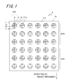
FIG. 1 is a plan view showing one embodiment of a light irradiation device; -
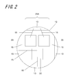
FIG. 2 is a plan view of the main part of the light irradiation device shown inFIG. 1 ; -
FIG. 3 is a sectional view of the light irradiation device taken along theline 1I-1I shown inFIG. 1 ; -
FIG. 4 is a view for explaining a method for centroid determination; -
FIG. 5 is a view for explaining a difference of light intensity per unit area; -
FIG. 6 is a sectional view showing the main part of a light irradiation module employing the light irradiation device shown inFIG. 1 ; -
FIG. 7 is a top view of a printing apparatus employing the light irradiation device shown inFIG. 1 ; -
FIG. 8 is a side view of the printing apparatus shown inFIG. 7 ; -
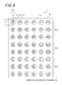
FIG. 9 is a view for explaining a first modified example of the light irradiation device shown inFIG. 1 ; and -
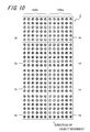
FIG. 10 is a view for explaining a second modified example of the light irradiation module shown inFIG. 6 . - Hereinafter, embodiments of a light irradiation device, a light irradiation module, and a printing apparatus according to the invention will be described with reference to drawings. It is noted that the following forms of the invention are given as illustrative only of embodiments of the invention, and thus the application of the invention is not limited to the embodiments as set forth herein.
- A light irradiation device of the present embodiment acts as an ultraviolet-producing light source which is incorporated into a printing apparatus, such as an offset printer or ink-jet printer using an ultraviolet curable ink, for applying ultraviolet light to a target object (recording medium) under relative movement after adhesion of an ultraviolet curable ink in order to cure the ultraviolet curable ink adherent to the object.
- As shown in
FIGS. 1 to 3 , alight irradiation device 1 comprises: abase 10 having a plurality ofopenings 12 formed in onemain surface 11a thereof; a plurality ofconnection pads 13 disposed inside each of theopenings 12; a plurality of light-emittingelements 20 disposed inside each of theopenings 12 of thebase 10 so as to be electrically connected to theconnection pads 13; a plurality ofsealing materials 30 filled in therespective openings 12 to cover the light-emittingelements 20; and a plurality oflenses 17 provided in correspondence to theopenings 12, respectively. - The
base 10 comprises: astacked body 40 in which a firstinsulating layer 41 and a secondinsulating layer 42 are laminated; andelectrical wiring 50 for providing connection between separate light-emitting elements 20. Thebase 10 is rectangular-shaped as seen in a plan view from above onemain surface 11a, and, the plurality of light-emittingelements 20 are supported within theopening 12 formed in the onemain surface 11a. - A plurality of (in this embodiment, three) light-emitting
elements 20 are placed inside each of theopenings 12, thereby constituting a light-emittingelement group 20A. These light-emitting element groups 20A of the present embodiment include: a plurality of first light-emitting element groups 20Aa located on an upstream side in a direction of object movement; and a plurality of second light-emitting element groups 20Ab located on a downstream side in the direction of object movement. - For example, the first insulating
layer 41 is made of ceramics such as an aluminum oxide sintered body, an aluminum nitride sintered body, a mullite sintered body, or glass ceramics, or a resin such as epoxy resin or a liquid crystal polymer (LCP). - The
electrical wiring 50 is formed, in a predetermined pattern, from an electrically conductive material such for example as tungsten(W), molybdenum (Mo), manganese (Mn), or copper (Cu), and acts as feeder wiring for supplying electric current to the light-emittingelement 20 or electric current from the light-emittingelement 20. - The second
insulating layer 42 laminated on the first insulatinglayer 41 has theopenings 12 formed so as to pass therethrough. - Each of the
openings 12 has an innerperipheral surface 14 inclined so that a hole diameter becomes larger gradually from a light-emitting element 20-placement surface to onemain surface 11a of thebase 10, and, as seen in a plan view, a shape of theopening 12 is defined by a circle, for example. Note that the opening shape is not limited to the circular shape, but may be of a rectangular shape. - Such an opening 12 acts as a reflection plate in which light emitted from the light-emitting
element 20 is reflected upwardly by the innerperipheral surface 14 for enhancement in light extraction efficiency. - In order to increase the light extraction efficiency, the second
insulating layer 42 may be formed of a porous ceramic material which exhibits a relatively good reflectivity to light in the ultraviolet range, for example, an aluminum oxide sintered body, a zirconium oxide sintered body, or an aluminum nitride sintered body. Moreover, from the viewpoint of increasing the light extraction efficiency, a metal-made reflection film may be provided on the innerperipheral surface 14 of theopening 12. - The
openings 12 are arranged in a matrix form over the entire area of the upper surface, or equivalently onemain surface 11a of thebase 10. In the present embodiment, theopenings 12 are placed in a rectangular lattice arrangement. - When it is desired to increase the intensity of light per unit area, for example, the openings may be placed in a staggered arrangement, that is; they are placed in zigzag form in plural rows, so that the light-emitting
elements 20, namely the light-emittingelement groups 20A can be arranged more densely. The term "staggered arrangement" is used herein for the same meaning as an arrangement such that the openings are located at lattice points of a slanting lattice. Moreover, the light-emittingelement group 20A composed of plural light-emittingelements 20 is placed inside theopening 12, wherefore the arrangement of theopenings 12 is construed as being equivalent to the arrangement of the light-emittingelement groups 20A. - In the present embodiment, the light-
emitting element group 20A is placed inside theopening 12, but, theopening 12 does not necessarily have to be provided, and therefore, a plurality of light-emittingelements 20 may be placed simply on the firstinsulating layer 41. Moreover, the secondinsulating layer 42 may be formed on the firstinsulating layer 41 as a thin layer which serves the purpose of providing protection for theelectrical wiring 50. - The
base 10 comprising thestacked body 40 composed of the first insulatinglayer 41 and the secondinsulating layer 42 thus far described is, in a case where the firstinsulating layer 41 and the secondinsulating layer 42 are made of ceramics or the like, produced by following procedural steps as set forth hereunder. - At first, a plurality of ceramic green sheets produced in a usual manner are prepared. A hole which serves as the
opening 12 is formed in an assigned ceramic green sheet by means of punching or otherwise. Next, after a metal paste which constitutes theelectrical wiring 50 is printed onto the green sheets (not shown in the drawing), the green sheets are laminated together so that the printed metal paste can be interposed between the green sheets. Exemplary of the metal paste constituting theelectrical wiring 50 is a paste containing a metal material such for example as tungsten(W), molybdenum (Mo), manganese (Mn), or copper (Cu). Next, the resultant laminate is fired, that is; the green sheets and the metal pastes are fired all together, whereupon thebase 10 having theelectrical wiring 50 and theopening 12 can be formed. - Moreover, in a case where the first
insulating layer 41 and the secondinsulating layer 42 are made of resin, for example, the following method can be considered as a way to produce thebase 10. - At first, precursor sheets of a thermosetting resin are prepared. Next, a metal-made lead terminal which constitutes the
electrical wiring 50 is placed between the precursor sheets, and the a plurality of precursor sheets are laminated together so that the lead terminal can be buried in the precursor sheets. Exemplary of the material constituting the lead terminal is a metal material such for example as copper (Cu), silver (Ag), aluminum (Al), an iron (Fe)-nickel (Ni)-cobalt (Co) alloy, or an iron (Fe)-nickel (Ni) alloy. After a hole which serves as theopening 12 is formed in the precursor sheets by means of lasering, etching, or otherwise, the precursor sheets are cured under heat, whereupon the production of thebase 10 is completed. In a case where theopening 12 is formed by means of lasering, the formation of theopening 12 may be carried out after curing the precursor sheets under heat. - Meanwhile, inside the
opening 12 of thebase 10, there are provided: a plurality ofconnection pads 13 electrically connected to a plurality of light-emittingelements 20; the plurality of light-emittingelements 20 connected to theconnection pads 13 via joiningmaterials 15 such as solder, gold (Au) wires, aluminum (Al) wires, or the like; and a sealingmaterial 30 for sealing the plurality of light-emittingelements 20. - The
connection pad 13 is constructed of a metal layer made of a metal material such for example as tungsten(W), molybdenum (Mo), manganese (Mn), or copper (Cu). Note that, for example, a nickel (Ni) layer, a palladium (Pd) layer, or a gold (Au) layer may additionally be laminated on the metal layer on an as needed basis. Such aconnection pad 13 is connected to the light-emittingelement 20 via the joiningmaterial 15 such as solder, a gold (Au) wire, an aluminum (Al) wire, or the like. - Moreover, for example, the light-emitting
element 20 is constructed of a light-emitting diode obtained by laminating an n-type semiconductor layer and a p-type semiconductor layer made of a semiconductor material such as gallium arsenide (GaAs) or gallium nitride (GaN) on anelement substrate 21 such as a sapphire substrate, or an organic EL element having an organic material-made semiconductor layer. - The light-emitting
element 20 comprises: asemiconductor layer 22 having a light-emitting layer; andelement electrodes connection pad 13 placed on thebase 10 via the joiningmaterial 15, and, the light-emittingelement 20 is connected to thebase 10 by means of wire bonding. In response to an electric current flowing between theelement electrodes element 20 emits light having a predetermined wavelength at a predetermined luminance. Note that theelement substrate 21 may be omitted. Moreover, the connection between theelement electrode element 20 and theconnection pad 13 may be effected by means of customary flip-chip bonding technique using solder as the joiningmaterial 15. - The present embodiment adopts a LED which serves as the light-emitting
element 20 for emitting UV light exhibiting a light emission spectrum whose peak wavelength falls in the range of, for example, 280 to 440 nm. That is, in the present embodiment, a UV-LED element is adopted for use as the light-emittingelement 20. Note that the light-emittingelement 20 is formed by means of commonly-used thin-film forming technique. - The light-emitting
element 20 is sealed by theaforementioned sealing material 30. - An insulating material such as a light-transmittable resin material is used as the sealing
material 30, and, by sealing the light-emittingelement 20 successfully, it is possible to prevent intrusion of moisture from outside, as well as to absorb external impact, and thereby provide protection for the light-emittingelement 20. - Moreover, the use of a material having a refractive index which falls in between the refractive index of the
element substrate 21 constituting the light-emitting element 20 (in the case of using a sapphire substrate, the refractive index is 1.7) and the refractive index of air (about 1.0), for example, the use of a silicone resin (refractive index: about 1.4) as the sealingmaterial 30 makes it possible to increase the efficiency of extraction of light from the light-emittingelement 20. - Such a sealing
material 30 can be formed by, after the light-emittingelement 20 is mounted on thebase 10, charging a precursor of a silicone resin or the like into theopening 12, and subsequently curing the resin. - The
lens 17 is disposed on the above-mentionedsealing material 30, via asecond adhesive 70, so as to cover the light-emittingelement group 20A. In thelight irradiation device 1 of the present embodiment, a plano-convex lens is used as theoptical lens 17. Thus, theoptical lens 17 of the present embodiment is so configured that one main surface is convexly curved, whereas the other main surface is made flat, that is; theoptical lens 17 is so shaped that its cross-sectional area becomes smaller gradually from the other main surface to one main surface. - The
optical lens 17, which is made for example of silicone, has the capability of condensing light emitted from the light-emittingelement group 20A. Examples of the material constituting the optical lens include, in addition to silicone as mentioned above, plastics such as a thermosetting resin such as urethane resin or epoxy resin, and a thermoplastic resin such as polycarbonate resin or acryl resin; sapphire; and inorganic glass. - Moreover, the
lenses 17 include: a plurality of first lenses 17a located on the upstream side in the direction of object movement; and a plurality of second lenses 17b located on the downstream side in the direction of object movement. The first lenses 17a are configured to cover the respective first light-emitting element groups 20Aa, and the second lenses 17b are configured to cover the respective second light-emitting element groups 20Ab. Hence, in the present embodiment, since the first light-emitting element groups 20Aa and the second light-emitting element groups 20Ab are placed in a rectangular lattice arrangement, it follows that an arrangement interval in the direction of object movement between the plurality of first lenses 17a and an arrangement interval in the direction of object movement between the plurality of second lenses 17b are equal to each other, as well as an arrangement interval in a direction perpendicular to the direction of object movement between the plurality of first lenses 17a and an arrangement interval in the direction perpendicular to the direction of object movement between the plurality of second lenses 17b are equal to each other. In this construction, it is possible to place the plurality of first lenses 17a and the plurality of second lenses 17b densely in a compact arrangement, and thereby conduce to downsizing of thelight irradiation device 1. - A center of each of the plurality of first lenses 17a as seen in a plan view is located at the downstream side in the direction of object direction with respect to a center of the respective first light-emitting element group 20Aa as seen in a plan view, and, a center of each of the plurality of second lenses 17b as seen in a plan view is located at the upstream side in the direction of object movement with respect to a center of the respective second light-emitting element group 20Ab as seen in a plan view.
- As employed herein, the term "center of each of the first light-emitting element group 20Aa and the second light-emitting element group 20Ab" refers to the centroid of the plan view showing the plurality of light-emitting
elements 20 provided in the first light-emitting element group 20Aa. The centroid is determined by dividing geometrical moment of area in a given point by total cross-sectional area. - A method for determining the centroid will be described specifically with reference to
FIG. 4 . -
FIG. 4 schematically shows three light-emittingelements 20 of the first light-emitting element group 20Aa of the present embodiment. The upper left-hand corner of the light-emittingelement 20 located in the upper left part ofFIG. 4 is defined as an origin O. Given that the cross-sectional areas of the upper-left light-emittingelement 20, the lower-central light-emittingelement 20, and the upper-right light-emittingelement 20 shown inFIG. 4 are defined as S1, S2, and S3, respectively, and that the distances between the centers of these light-emittingelements 20 and x axis (in the case shown inFIG. 4 , the center coincides with the intersection point of diagonal lines drawn in each light-emitting element 20) are defined as y1, y2, and y1, respectively, then a moment about the x axis with respect to the origin O is expressed as: y1 × S1 + y2 × S2 + y1 × S3. This moment is geometrical moment of area, and, a y-coordinate of the centroid yG is derived by dividing the geometrical moment of area by the total area expressed as: S1 + S2 + S3. That is, the following equation holds: yG = (y1 × S1 + y2 × S2 + y1 × S3)/(S1 + S2 + S3). - Similarly, given that the distances between the centers of the light-emitting
elements 20 and y axis are defined as x1, x2, and x3, respectively, then a moment about the y axis with respect to the origin O is expressed as: x1 × S1 + x2 × S2 + x3 × S3. An x-coordinate of the centroid xG is derived by dividing the moment by the total area expressed as: S1 + S2 + S3. That is, the following equation holds: xG = (x1 × S1 + x2 × S2 + x3 × S3)/(S1 + S2 + S3). - Moreover, the center of each of the first lens 17a and the second lens 17b refers to the center of the bottom surface of each lens.
- By arranging the first light-emitting element group 20Aa and the first lens 17a in that way, the optical axis of light emitted from the light-emitting element group 20Aa through the first lens 17a is inclined toward the downstream side in the direction of object movement with respect to the normal to the upper surface of the base 10 (one
main surface 11a), and also, by arranging the second light-emitting element group 20Ab and the second lens 17b in that way, the optical axis of light emitted from the light-emitting element group 20Ab through the second lens 17b is inclined toward the upstream side in the direction of object movement with respect to the normal to the upper surface of the base 10 (onemain surface 11a). As a result, the intensity of light per unit area emitted from thelight irradiation device 1 can be increased on a target object. -
FIG. 5 schematically shows light intensity per unit area of thelight irradiation device 1 in the direction of object movement. A solid line indicates the intensity of light per unit area as found in the case where the first light-emitting element group 20Aa and the first lens 17a, as well as the second light-emitting element group 20Ab and the second lens 17b, are arranged in a manner as practiced in the present embodiment, whereas a broken line indicates the intensity of light per unit area as found in a case where the center of the first light-emitting element group 20Aa is brought into coincidence with the center of the first lens 17a, and the center of the second light-emitting element group 20Ab is brought into coincidence with the center of the second lens 17b. - The area of a region enclosed by the horizontal axis and the solid line and the area of a region enclosed by the horizontal axis and the broken line each represent integral light energy, and, the former region and the latter region, while being equal to each other in respect of integral light energy, differ from each other in respect of the maximum value of light intensity per unit area. That is, the
light irradiation device 1 of the present embodiment is capable of enhancement in light intensity per unit area. - As employed herein, the term "light intensity per unit area" refers to the intensity of light per unit area on a target object, and it may advisably be measured by a heretofore known method, namely by setting the light-receiving section of an ultraviolet meter on a target object. The intensity of light per unit area is also called "irradiance", and a unit of irradiance is W/cm2, for example.
- In the present embodiment, the optical axis of light emitted from the first light-emitting element group 20Aa through the first lens 17a and the optical axis of light emitted from the second light-emitting element group 20Ab through the second lens 17b are identically inclined with respect to the normal to the upper surface of the base 10 (one
main surface 11a). - Further enhancement of light intensity per unit area can be achieved by making a degree of inclination of the optical axis of light emitted from the first light-emitting element group 20Aa through the first lens 17a with respect to the normal to the upper surface of the base 10 (one
main surface 11a) smaller gradually from the upstream side to the downstream side in the direction of object movement, and making a degree of inclination of the optical axis of light emitted from the second light-emitting element group 20Ab through the second lens 17b with respect to the normal to the upper surface of the base 10 (onemain surface 11a) smaller gradually from the downstream side to the upstream side in the direction of object movement. - As shown in
FIG. 6 , alight irradiation module 2 of the present embodiment comprises; a heat-dissipatingmember 110; and thelight irradiation device 1 placed on the heat-dissipatingmember 110. Thelight irradiation device 1 is placed on the main surface of the heat-dissipatingmember 110, via an adhesive 120 such as silicone resin or epoxy resin. - The heat-dissipating
member 110 acts as a support for thelight irradiation device 1, and also as a heat dissipator for dissipating heat liberated from thelight irradiation device 1 to the outside. As the material constituting the heat-dissipatingmember 110, a material having high heat conductivity, for example, metal materials, ceramics, and resin materials of various types are desirable for use. In the present embodiment, the heat-dissipatingmember 110 is made of copper. - According to the
light irradiation module 2 of the present embodiment, it is possible to afford the above-mentioned advantageous effects produced by thelight irradiation device 1. - As shown in
FIGS. 7 and 8 , aprinting apparatus 200 of the present embodiment comprises: a conveyingpart 210 for conveying arecording medium 250; aprinting part 220 which acts as a printing mechanism for printing on therecording medium 250 under conveyance; the above-mentionedlight irradiation device 1 for applying ultraviolet light to therecording medium 250 printed; and acontrol system 230 for controlling emission of light from thelight irradiation device 1. Therecording medium 250 is equivalent to the target object thus far described. - The conveying
part 210, which is intended to convey therecording medium 250 in a manner such that is passes through theprinting part 220 and thelight irradiation device 1 sequentially in the order named, comprises: a placement table 211; and conveyingrollers 212, taken as a pair, set face to face with each other while being rotatably supported. In the conveyingpart 210, therecording medium 250 supported by the placement table 211 is fed to a space between the paired conveyingrollers 212, and, upon rotation of the conveyingrollers 212, therecording medium 250 is conveyed in a conveyance direction. - The
printing part 220 has the capability of adhering a photosensitive material to therecording medium 250 which is being conveyed via the conveyingpart 210. Theprinting part 220 discharges droplets containing the photosensitive material to therecording medium 250, thereby adhering the photosensitive material to therecording medium 250. In the present embodiment, an ultraviolet curable ink is adopted for use as the photosensitive material. Examples of the photosensitive material include, in addition to the ultraviolet curable ink, a photoresist and a photocurable resin. - In the present embodiment, line-type printing part is adopted for use as the
printing part 220. Theprinting part 220 has a plurality ofdischarge holes 220a linearly arranged in a main scanning direction, so that the ultraviolet curable ink can be discharged from thesedischarge holes 220a. Theprinting part 220 is configured to print on the recording medium by discharging the ink through the discharge holes 220a for adhesion of the ink to therecording medium 250 which is being conveyed in a direction perpendicular to the array of the discharge holes 220a (a sub scanning direction). - Although the line-type printing part exemplifies the printing mechanism in the present embodiment, for example, serial-type printing part, or a line-type or serial-type spraying head (for example, ink-jet head) may be adopted instead. It is also possible to adopt, as the printing mechanism, an electrostatic head in which static electricity is caused to accumulate in the
recording medium 250 for adhesion of a photosensitive material to therecording medium 250 under the static electricity, or an immersion device in which therecording medium 250 is immersed in a photosensitive material in liquid form for adhesion of the photosensitive material to therecording medium 250. Moreover, a brush coater, a brush, a roller, and the like can be adopted for use as the printing mechanism. - In the
printing apparatus 200, thelight irradiation device 1 performs the function of exposing the photosensitive material adherent to therecording medium 250 which is being conveyed via the conveyingpart 210 to light. Thelight irradiation device 1 is located at the downstream side in the conveyance direction with respect to theprinting part 220. Moreover, in theprinting apparatus 200, the light-emittingelement 20 performs the function of exposing the photosensitive material adherent to therecording medium 250 to light. - The
control system 230 performs the function of controlling emission of light from thelight irradiation device 1. In a memory of thecontrol system 230, there is stored information indicative of characteristics of light which allows ink droplets discharged from theprinting part 220 to cure in a relatively satisfactory manner. Specific examples of the information stored in the memory include wavelength distribution characteristics and numerical values representing light emission intensity (emission intensity in each wavelength range) suited to curing the discharge of ink droplets. By virtue of thiscontrol system 230, theprinting apparatus 200 of the present embodiment is also capable of making adjustment to the magnitude of driving current which is inputted to a plurality of light-emittingelements 20 on the basis of the information stored in thecontrol system 230. Thus, according to theprinting apparatus 200 of the present embodiment, it is possible to achieve irradiation of light with adequate ultraviolet irradiation energy conforming to the characteristics of an ink in use, and thereby cure ink droplets with light of relatively low energy. - In the
printing apparatus 200, the conveyingpart 210 conveys therecording medium 250 in the conveyance direction. Theprinting part 220 discharges an ultraviolet curable ink to therecording medium 250 under conveyance for adhesion of the ultraviolet curable ink to the surface of therecording medium 250. At this time, the ultraviolet curable ink which is caused to adhere to therecording medium 250 may be applied to either the entire area or part of the area of therecording medium 250, or may be applied in a predetermined adherent pattern to therecording medium 250. In thisprinting apparatus 200, the ultraviolet curable ink adherent to therecording medium 250 is cured under irradiation of ultraviolet rays emitted from thelight irradiation device 1. - According to the
printing apparatus 200 of the present embodiment, it is possible to afford the above-mentioned advantageous effects produced by thelight irradiation device 1. - Although specific embodiments of the invention have been shown herein, it will be understood that the invention is not so limited, and thus many changes and modifications are possible without departing from the scope of the invention.
- For example, as in a first modified example shown in
FIG. 9 , a plurality of third light-emitting element groups 20Ac and a plurality of third lenses 17c corresponding thereto may additionally be disposed between the plurality of first light-emitting element groups 20Aa and the plurality of second light-emitting element groups 20Ab. In this case, an optical axis of light emitted through each of the plurality of third lenses 17c runs in a direction along the normal to the upper surface of the base 10 (onemain surface 11a). That is, in a plan view, the center of each of the plurality of third lenses 17c is located at the center of its respective third light-emitting element group 20Ac. In this construction, further enhancement in light intensity per unit area can be achieved. - In the first modified example, the third light-emitting element group 20Ac is composed of four light-emitting
elements 20, that is; the number of the light-emittingelements 20 constituting the third light-emitting element group 20Ac is greater than the number of the light-emittingelements 20 constituting each of the first light-emitting element group 20Aa and the second light-emitting element group 20Ab. In this construction, as compared with a case where the first light-emitting element group 20Aa, the second light-emitting element group 20Ab, and the third light-emitting element group 20Ac are equal in the number of constituent light-emittingelements 20, higher light intensity per unit area can be attained. - Although, in the first modified example, the number of the light-emitting
elements 20 constituting the third light-emitting element group 20Ac is greater than the number of the light-emittingelements 20 constituting each of the first light-emitting element group 20Aa and the second light-emitting element group 20Ab, on the contrary, the third light-emitting element group 20Ac may have a fewer number of light-emittingelements 20 than those of the first and second light-emitting element groups in so far as a necessary level of light intensity per unit area can be attained. As a matter of course, the first light-emitting element group 20Aa, the second light-emitting element group 20Ab, and the third light-emitting element group 20Ac do not necessarily have to be equal in the number of constituent light-emittingelements 20, and thus, the number of the light-emittingelements 20 can be adjusted on an as needed basis. - Moreover, for example, as in a second modified example of the
light irradiation module 2 of the present embodiment as shown inFIG. 10 , a plurality oflight irradiation devices 1 constituting thelight irradiation modules 2 may be arranged both in the direction of object movement and in a width direction perpendicular to the direction of object movement. In the second modified example, fourlight irradiation devices 1 are arranged in the width direction, and twolight irradiation devices 1 are arranged in the direction of object movement. In this case, thelight irradiation devices 1 are configured bylight irradiation devices 1A located on the upstream side in the direction of object movement andlight irradiation devices 1B located on the downstream side in the direction of object movement. Thelight irradiation device 1A is composed of the first light-emitting element groups 20Aa, and thelight irradiation device 1B is composed of the second light-emitting element groups 20Ab. Thelight irradiation module 2 thereby constructed is capable of affording the same effects as achieved in thelight irradiation device 1. - Moreover, the
printing apparatus 200 of the present embodiment may be built as, for example, a so-called offset printer in which a roller supported by a shaft thereof is rotated so that a recording medium can be conveyed along a surface of the roller. Also in this case, the same effects can be attained. - Although the above-mentioned embodiment is exemplified by a construction implemented by applying the
light irradiation device 1 to theprinting apparatus 200 employing the ink-jet head 220, thelight irradiation device 1 can find applications also in devices for curing various types of photocurable resins, for example, a specific-purpose curing device for curing a photocurable resin spin-coated to the surface of a target object. Moreover, thelight irradiation device 1 may be used as an irradiation light source provided in an exposure device. - It is obviously needless to say that the
light irradiation module 2 can be applied to theprinting apparatus 200 instead of thelight irradiation device 1. -
- 1: Light irradiation device
- 2: Light irradiation module
- 10: Base
- 11a: One main surface
- 12: Opening
- 13: Connection pad
- 14: Inner peripheral surface
- 15: Joining material
- 17: Lens
- 17a: First lens
- 17b: Second lens
- 17: Lens adhesive
- 20: Light-emitting element
- 20A: Light-emitting element group
- 20Aa: First light-emitting element group
- 20Ab: Second light-emitting element group
- 21: Element substrate
- 22: Semiconductor layer
- 23, 24: Element electrode
- 30: Sealing material
- 40: Stacked body
- 41: First insulating layer
- 42: Second insulating layer
- 50: Electrical wiring
- 110: Heat-dissipating member
- 120: Adhesive
- 200: Printing apparatus
- 210: Conveying part
- 211: Placement table
- 212: Conveying roller
- 220: Printing part
- 220a: Discharge hole
- 230: Control system
- 250: Recording medium
Claims (9)
- A light irradiation device for applying light to a target object under relative movement, comprising:a base;a plurality of light-emitting element groups, each of groups having a plurality of light-emitting elements, the plurality of light-emitting elements being arranged in a matrix form on an upper surface of the base; anda plurality of lenses configured to cover the light-emitting element groups, respectively, the plurality of lenses radiating light emitted from the light-emitting element groups outwardly, whereinthe plurality of light-emitting element groups comprise
a plurality of first light-emitting element groups located on an upstream side in a movement direction in which the target object is moved relative to the light irradiation device, and
a plurality of second light-emitting element groups located on a downstream side in the movement direction,the plurality of lenses comprise
a plurality of first lenses which cover the plurality of first light-emitting element groups, respectively, and
a plurality of second lenses which cover the plurality of second light-emitting element groups, respectively,an optical axis of light emitted through each of the plurality of first lenses is inclined toward the downstream side in the movement direction with respect to a normal to the upper surface of the base, andan optical axis of light emitted through each of the plurality of second lenses is inclined toward the upstream side in the movement direction with respect to a normal to the upper surface of the base. - The light irradiation device according to claim 1,
wherein a center of each of the plurality of first lenses as seen in a plan view is located at the downstream side in the movement direction with respect to a center of the first light-emitting element group corresponding to the each of the plurality of first lenses as seen in a plan view, and
a center of each of the plurality of second lenses as seen in a plan view is located at the upstream side in the movement direction with respect to a center of the second light-emitting element group corresponding to the each of the plurality of second lenses as seen in a plan view. - The light irradiation device according to claim 1 or 2,
wherein an arrangement interval in the movement direction between the plurality of first lenses and an arrangement interval in the movement direction between the plurality of second lenses are equal to each other. - The light irradiation device according to any one of claims 1 to 3,
wherein a degree of inclination of the optical axis of light emitted through each of the plurality of first lenses with respect to the normal to the upper surface of the base becomes smaller gradually from the upstream side to the downstream side in the movement direction, and
a degree of inclination of the optical axis of light emitted through each of the plurality of second lenses with respect to the normal to the upper surface of the base becomes smaller gradually from the downstream side to the upstream side in the movement direction. - The light irradiation device according to any one of claims 1 to 4, further comprising:a plurality of third light-emitting element groups and a plurality of third lenses corresponding to the plurality of third light-emitting element groups, respectively, the plurality of third light-emitting element groups and the plurality of third lenses being disposed between the plurality of first light-emitting element groups and the plurality of second light-emitting element groups,wherein an optical axis of light emitted through each of the plurality of third lenses runs in a direction along the normal to the upper surface of the base.
- The light irradiation device according to claim 5,
wherein a center of each of the plurality of third lenses as seen in a plan view is located at a center of the third light-emitting element group corresponding to the each of the plurality of third lenses as seen in a plan view. - The light irradiation device according to claim 5 or 6,
wherein an arrangement interval in the movement direction between the plurality of first lenses, an arrangement interval in the movement direction between the plurality of second lenses, and an arrangement interval in the movement direction between the plurality of third lenses are equal to one another. - A light irradiation module, comprising:a heat-dissipating member; anda plurality of light irradiation devices according to any one of claims 1 to 6, the plurality of light irradiation devices being disposed on the heat-dissipating member.
- A printing apparatus, comprising:a printing part configured to print on a recording medium; andthe light irradiation module according to claim 7, the light irradiation module applying light to a recording medium printed.
Applications Claiming Priority (2)
| Application Number | Priority Date | Filing Date | Title |
|---|---|---|---|
| JP2012260500 | 2012-11-29 | ||
| PCT/JP2013/081530 WO2014084143A1 (en) | 2012-11-29 | 2013-11-22 | Light irradiation device, light irradiation module and printing device |
Publications (3)
| Publication Number | Publication Date |
|---|---|
| EP2926895A1 true EP2926895A1 (en) | 2015-10-07 |
| EP2926895A4 EP2926895A4 (en) | 2016-07-27 |
| EP2926895B1 EP2926895B1 (en) | 2020-04-01 |
Family
ID=50827781
Family Applications (1)
| Application Number | Title | Priority Date | Filing Date |
|---|---|---|---|
| EP13859410.6A Active EP2926895B1 (en) | 2012-11-29 | 2013-11-22 | Light irradiation device, light irradiation module and printing device |
Country Status (4)
| Country | Link |
|---|---|
| US (1) | US9487019B2 (en) |
| EP (1) | EP2926895B1 (en) |
| JP (1) | JPWO2014084143A1 (en) |
| WO (1) | WO2014084143A1 (en) |
Families Citing this family (3)
| Publication number | Priority date | Publication date | Assignee | Title |
|---|---|---|---|---|
| CN104190344B (en) * | 2014-07-25 | 2016-01-13 | 北京泊菲莱科技有限公司 | Light irradiation multi-sample parallel reaction device |
| JP2016137475A (en) * | 2015-01-29 | 2016-08-04 | 京セラ株式会社 | Light irradiation apparatus, and printing apparatus |
| JP6517721B2 (en) * | 2016-03-18 | 2019-05-22 | Hoya Candeo Optronics株式会社 | Light irradiation device |
Family Cites Families (13)
| Publication number | Priority date | Publication date | Assignee | Title |
|---|---|---|---|---|
| JPH08116041A (en) * | 1994-10-13 | 1996-05-07 | Olympus Optical Co Ltd | Manufacture of solid-state image sensing device |
| JPH09164717A (en) * | 1995-12-15 | 1997-06-24 | Stanley Electric Co Ltd | Head for optical printer |
| CN1464953A (en) | 2001-08-09 | 2003-12-31 | 松下电器产业株式会社 | LED lighting device and card type LED lighting source |
| JP3989794B2 (en) | 2001-08-09 | 2007-10-10 | 松下電器産業株式会社 | LED illumination device and LED illumination light source |
| US8251689B2 (en) * | 2005-09-20 | 2012-08-28 | Summit Business Products, Inc. | Ultraviolet light-emitting diode device |
| JP4816367B2 (en) * | 2006-09-27 | 2011-11-16 | ウシオ電機株式会社 | Light irradiator and inkjet printer |
| US7959282B2 (en) | 2007-12-20 | 2011-06-14 | Summit Business Products, Inc. | Concentrated energy source |
| JP5421799B2 (en) * | 2010-01-18 | 2014-02-19 | パナソニック株式会社 | LED unit |
| JP5473673B2 (en) * | 2010-02-26 | 2014-04-16 | 京セラ株式会社 | Light emitting element array and printing apparatus |
| JP2011204397A (en) * | 2010-03-24 | 2011-10-13 | Sony Corp | Lighting system |
| US9012938B2 (en) * | 2010-04-09 | 2015-04-21 | Cree, Inc. | High reflective substrate of light emitting devices with improved light output |
| JP5582967B2 (en) * | 2010-10-27 | 2014-09-03 | 京セラ株式会社 | Light irradiation apparatus, light irradiation module, and printing apparatus |
| JP2012114384A (en) * | 2010-11-29 | 2012-06-14 | Kyocera Corp | Light irradiation device and printing device |
-
2013
- 2013-11-22 WO PCT/JP2013/081530 patent/WO2014084143A1/en not_active Ceased
- 2013-11-22 JP JP2014550163A patent/JPWO2014084143A1/en active Pending
- 2013-11-22 EP EP13859410.6A patent/EP2926895B1/en active Active
- 2013-11-22 US US14/647,326 patent/US9487019B2/en not_active Expired - Fee Related
Also Published As
| Publication number | Publication date |
|---|---|
| JPWO2014084143A1 (en) | 2017-01-05 |
| EP2926895B1 (en) | 2020-04-01 |
| WO2014084143A1 (en) | 2014-06-05 |
| EP2926895A4 (en) | 2016-07-27 |
| US20150314614A1 (en) | 2015-11-05 |
| US9487019B2 (en) | 2016-11-08 |
Similar Documents
| Publication | Publication Date | Title |
|---|---|---|
| US9004667B2 (en) | Light irradiation device, light irradiation module, and printing apparatus | |
| JP5826115B2 (en) | Light irradiation device, light irradiation module, and printing apparatus | |
| JP6325271B2 (en) | Light irradiation apparatus and printing apparatus | |
| JP2012091123A (en) | Light irradiation device, light irradiation module, and printing device | |
| JP2014165333A (en) | Light emission device, light emission module and printer | |
| JP2014090055A (en) | Light irradiation module and printer | |
| US9561643B2 (en) | Light irradiation apparatus and printing apparatus | |
| EP2926895B1 (en) | Light irradiation device, light irradiation module and printing device | |
| JP2012049453A (en) | Light irradiation device, light irradiation module and printer | |
| EP3370269B1 (en) | Light irradiation device and light irradiation system | |
| JP5766008B2 (en) | Light irradiation module, light irradiation apparatus and printing apparatus | |
| JP2012114384A (en) | Light irradiation device and printing device | |
| JP2012245750A (en) | Light irradiation module and printing device | |
| JP5675506B2 (en) | Light irradiation device, light irradiation module, and printing apparatus | |
| JP5586327B2 (en) | Surface-emitting type irradiation device, surface-emitting type irradiation module, and printing apparatus | |
| JP5902568B2 (en) | Light irradiation device and printing apparatus | |
| WO2016158808A1 (en) | Light irradiation device and printing device | |
| JP2013171911A (en) | Light radiation module and printing device | |
| JP5848092B2 (en) | Light irradiation apparatus and printing apparatus | |
| JP2012071509A (en) | Light irradiation device, light irradiation module, and printer | |
| JP2013074226A (en) | Light irradiation module and printer | |
| JP2012205984A (en) | Light irradiation module and printing device | |
| JP6342955B2 (en) | Light irradiation apparatus and printing apparatus | |
| JP2014192403A (en) | Light irradiation device, light irradiation module and printer | |
| JP2015012119A (en) | Light irradiation device, light irradiation module, and printing apparatus |
Legal Events
| Date | Code | Title | Description |
|---|---|---|---|
| PUAI | Public reference made under article 153(3) epc to a published international application that has entered the european phase |
Free format text: ORIGINAL CODE: 0009012 |
|
| 17P | Request for examination filed |
Effective date: 20150526 |
|
| AK | Designated contracting states |
Kind code of ref document: A1 Designated state(s): AL AT BE BG CH CY CZ DE DK EE ES FI FR GB GR HR HU IE IS IT LI LT LU LV MC MK MT NL NO PL PT RO RS SE SI SK SM TR |
|
| AX | Request for extension of the european patent |
Extension state: BA ME |
|
| DAX | Request for extension of the european patent (deleted) | ||
| RA4 | Supplementary search report drawn up and despatched (corrected) |
Effective date: 20160624 |
|
| RIC1 | Information provided on ipc code assigned before grant |
Ipc: G02B 19/00 20060101ALI20160620BHEP Ipc: B41J 2/01 20060101ALI20160620BHEP Ipc: F21S 2/00 20160101ALI20160620BHEP Ipc: B41J 11/00 20060101ALN20160620BHEP Ipc: F21V 5/04 20060101ALI20160620BHEP Ipc: G02B 3/00 20060101ALI20160620BHEP Ipc: H01L 33/58 20100101ALN20160620BHEP Ipc: F21V 5/00 20150101ALI20160620BHEP Ipc: B41F 23/04 20060101ALI20160620BHEP Ipc: B01J 19/12 20060101AFI20160620BHEP Ipc: C08J 3/28 20060101ALI20160620BHEP |
|
| RIC1 | Information provided on ipc code assigned before grant |
Ipc: B01J 19/12 20060101AFI20190918BHEP Ipc: F21S 2/00 20160101ALI20190918BHEP Ipc: G02B 19/00 20060101ALI20190918BHEP Ipc: F21V 5/00 20180101ALI20190918BHEP Ipc: B41J 2/01 20060101ALI20190918BHEP Ipc: H01L 33/58 20100101ALN20190918BHEP Ipc: C08J 3/28 20060101ALI20190918BHEP Ipc: F21V 5/04 20060101ALI20190918BHEP Ipc: B41J 11/00 20060101ALN20190918BHEP Ipc: G02B 3/00 20060101ALI20190918BHEP Ipc: B41F 23/04 20060101ALI20190918BHEP |
|
| RIC1 | Information provided on ipc code assigned before grant |
Ipc: G02B 3/00 20060101ALI20190923BHEP Ipc: B01J 19/12 20060101AFI20190923BHEP Ipc: F21V 5/00 20180101ALI20190923BHEP Ipc: C08J 3/28 20060101ALI20190923BHEP Ipc: F21V 5/04 20060101ALI20190923BHEP Ipc: G02B 19/00 20060101ALI20190923BHEP Ipc: H01L 33/58 20100101ALN20190923BHEP Ipc: B41F 23/04 20060101ALI20190923BHEP Ipc: B41J 11/00 20060101ALN20190923BHEP Ipc: B41J 2/01 20060101ALI20190923BHEP Ipc: F21S 2/00 20160101ALI20190923BHEP |
|
| GRAP | Despatch of communication of intention to grant a patent |
Free format text: ORIGINAL CODE: EPIDOSNIGR1 |
|
| STAA | Information on the status of an ep patent application or granted ep patent |
Free format text: STATUS: GRANT OF PATENT IS INTENDED |
|
| INTG | Intention to grant announced |
Effective date: 20191108 |
|
| GRAS | Grant fee paid |
Free format text: ORIGINAL CODE: EPIDOSNIGR3 |
|
| GRAA | (expected) grant |
Free format text: ORIGINAL CODE: 0009210 |
|
| STAA | Information on the status of an ep patent application or granted ep patent |
Free format text: STATUS: THE PATENT HAS BEEN GRANTED |
|
| AK | Designated contracting states |
Kind code of ref document: B1 Designated state(s): AL AT BE BG CH CY CZ DE DK EE ES FI FR GB GR HR HU IE IS IT LI LT LU LV MC MK MT NL NO PL PT RO RS SE SI SK SM TR |
|
| REG | Reference to a national code |
Ref country code: GB Ref legal event code: FG4D |
|
| REG | Reference to a national code |
Ref country code: AT Ref legal event code: REF Ref document number: 1250652 Country of ref document: AT Kind code of ref document: T Effective date: 20200415 Ref country code: CH Ref legal event code: EP |
|
| REG | Reference to a national code |
Ref country code: DE Ref legal event code: R096 Ref document number: 602013067536 Country of ref document: DE |
|
| REG | Reference to a national code |
Ref country code: IE Ref legal event code: FG4D |
|
| PG25 | Lapsed in a contracting state [announced via postgrant information from national office to epo] |
Ref country code: BG Free format text: LAPSE BECAUSE OF FAILURE TO SUBMIT A TRANSLATION OF THE DESCRIPTION OR TO PAY THE FEE WITHIN THE PRESCRIBED TIME-LIMIT Effective date: 20200701 |
|
| REG | Reference to a national code |
Ref country code: NL Ref legal event code: MP Effective date: 20200401 |
|
| REG | Reference to a national code |
Ref country code: LT Ref legal event code: MG4D |
|
| PG25 | Lapsed in a contracting state [announced via postgrant information from national office to epo] |
Ref country code: FI Free format text: LAPSE BECAUSE OF FAILURE TO SUBMIT A TRANSLATION OF THE DESCRIPTION OR TO PAY THE FEE WITHIN THE PRESCRIBED TIME-LIMIT Effective date: 20200401 Ref country code: IS Free format text: LAPSE BECAUSE OF FAILURE TO SUBMIT A TRANSLATION OF THE DESCRIPTION OR TO PAY THE FEE WITHIN THE PRESCRIBED TIME-LIMIT Effective date: 20200801 Ref country code: SE Free format text: LAPSE BECAUSE OF FAILURE TO SUBMIT A TRANSLATION OF THE DESCRIPTION OR TO PAY THE FEE WITHIN THE PRESCRIBED TIME-LIMIT Effective date: 20200401 Ref country code: NO Free format text: LAPSE BECAUSE OF FAILURE TO SUBMIT A TRANSLATION OF THE DESCRIPTION OR TO PAY THE FEE WITHIN THE PRESCRIBED TIME-LIMIT Effective date: 20200701 Ref country code: GR Free format text: LAPSE BECAUSE OF FAILURE TO SUBMIT A TRANSLATION OF THE DESCRIPTION OR TO PAY THE FEE WITHIN THE PRESCRIBED TIME-LIMIT Effective date: 20200702 Ref country code: PT Free format text: LAPSE BECAUSE OF FAILURE TO SUBMIT A TRANSLATION OF THE DESCRIPTION OR TO PAY THE FEE WITHIN THE PRESCRIBED TIME-LIMIT Effective date: 20200817 Ref country code: LT Free format text: LAPSE BECAUSE OF FAILURE TO SUBMIT A TRANSLATION OF THE DESCRIPTION OR TO PAY THE FEE WITHIN THE PRESCRIBED TIME-LIMIT Effective date: 20200401 Ref country code: CZ Free format text: LAPSE BECAUSE OF FAILURE TO SUBMIT A TRANSLATION OF THE DESCRIPTION OR TO PAY THE FEE WITHIN THE PRESCRIBED TIME-LIMIT Effective date: 20200401 Ref country code: NL Free format text: LAPSE BECAUSE OF FAILURE TO SUBMIT A TRANSLATION OF THE DESCRIPTION OR TO PAY THE FEE WITHIN THE PRESCRIBED TIME-LIMIT Effective date: 20200401 |
|
| REG | Reference to a national code |
Ref country code: AT Ref legal event code: MK05 Ref document number: 1250652 Country of ref document: AT Kind code of ref document: T Effective date: 20200401 |
|
| PG25 | Lapsed in a contracting state [announced via postgrant information from national office to epo] |
Ref country code: RS Free format text: LAPSE BECAUSE OF FAILURE TO SUBMIT A TRANSLATION OF THE DESCRIPTION OR TO PAY THE FEE WITHIN THE PRESCRIBED TIME-LIMIT Effective date: 20200401 Ref country code: LV Free format text: LAPSE BECAUSE OF FAILURE TO SUBMIT A TRANSLATION OF THE DESCRIPTION OR TO PAY THE FEE WITHIN THE PRESCRIBED TIME-LIMIT Effective date: 20200401 Ref country code: HR Free format text: LAPSE BECAUSE OF FAILURE TO SUBMIT A TRANSLATION OF THE DESCRIPTION OR TO PAY THE FEE WITHIN THE PRESCRIBED TIME-LIMIT Effective date: 20200401 |
|
| PG25 | Lapsed in a contracting state [announced via postgrant information from national office to epo] |
Ref country code: AL Free format text: LAPSE BECAUSE OF FAILURE TO SUBMIT A TRANSLATION OF THE DESCRIPTION OR TO PAY THE FEE WITHIN THE PRESCRIBED TIME-LIMIT Effective date: 20200401 |
|
| REG | Reference to a national code |
Ref country code: DE Ref legal event code: R097 Ref document number: 602013067536 Country of ref document: DE |
|
| PG25 | Lapsed in a contracting state [announced via postgrant information from national office to epo] |
Ref country code: DK Free format text: LAPSE BECAUSE OF FAILURE TO SUBMIT A TRANSLATION OF THE DESCRIPTION OR TO PAY THE FEE WITHIN THE PRESCRIBED TIME-LIMIT Effective date: 20200401 Ref country code: AT Free format text: LAPSE BECAUSE OF FAILURE TO SUBMIT A TRANSLATION OF THE DESCRIPTION OR TO PAY THE FEE WITHIN THE PRESCRIBED TIME-LIMIT Effective date: 20200401 Ref country code: IT Free format text: LAPSE BECAUSE OF FAILURE TO SUBMIT A TRANSLATION OF THE DESCRIPTION OR TO PAY THE FEE WITHIN THE PRESCRIBED TIME-LIMIT Effective date: 20200401 Ref country code: ES Free format text: LAPSE BECAUSE OF FAILURE TO SUBMIT A TRANSLATION OF THE DESCRIPTION OR TO PAY THE FEE WITHIN THE PRESCRIBED TIME-LIMIT Effective date: 20200401 Ref country code: RO Free format text: LAPSE BECAUSE OF FAILURE TO SUBMIT A TRANSLATION OF THE DESCRIPTION OR TO PAY THE FEE WITHIN THE PRESCRIBED TIME-LIMIT Effective date: 20200401 Ref country code: EE Free format text: LAPSE BECAUSE OF FAILURE TO SUBMIT A TRANSLATION OF THE DESCRIPTION OR TO PAY THE FEE WITHIN THE PRESCRIBED TIME-LIMIT Effective date: 20200401 Ref country code: SM Free format text: LAPSE BECAUSE OF FAILURE TO SUBMIT A TRANSLATION OF THE DESCRIPTION OR TO PAY THE FEE WITHIN THE PRESCRIBED TIME-LIMIT Effective date: 20200401 |
|
| PLBE | No opposition filed within time limit |
Free format text: ORIGINAL CODE: 0009261 |
|
| STAA | Information on the status of an ep patent application or granted ep patent |
Free format text: STATUS: NO OPPOSITION FILED WITHIN TIME LIMIT |
|
| PG25 | Lapsed in a contracting state [announced via postgrant information from national office to epo] |
Ref country code: SK Free format text: LAPSE BECAUSE OF FAILURE TO SUBMIT A TRANSLATION OF THE DESCRIPTION OR TO PAY THE FEE WITHIN THE PRESCRIBED TIME-LIMIT Effective date: 20200401 Ref country code: PL Free format text: LAPSE BECAUSE OF FAILURE TO SUBMIT A TRANSLATION OF THE DESCRIPTION OR TO PAY THE FEE WITHIN THE PRESCRIBED TIME-LIMIT Effective date: 20200401 |
|
| 26N | No opposition filed |
Effective date: 20210112 |
|
| PG25 | Lapsed in a contracting state [announced via postgrant information from national office to epo] |
Ref country code: SI Free format text: LAPSE BECAUSE OF FAILURE TO SUBMIT A TRANSLATION OF THE DESCRIPTION OR TO PAY THE FEE WITHIN THE PRESCRIBED TIME-LIMIT Effective date: 20200401 |
|
| PG25 | Lapsed in a contracting state [announced via postgrant information from national office to epo] |
Ref country code: MC Free format text: LAPSE BECAUSE OF FAILURE TO SUBMIT A TRANSLATION OF THE DESCRIPTION OR TO PAY THE FEE WITHIN THE PRESCRIBED TIME-LIMIT Effective date: 20200401 |
|
| REG | Reference to a national code |
Ref country code: CH Ref legal event code: PL |
|
| GBPC | Gb: european patent ceased through non-payment of renewal fee |
Effective date: 20201122 |
|
| PG25 | Lapsed in a contracting state [announced via postgrant information from national office to epo] |
Ref country code: LU Free format text: LAPSE BECAUSE OF NON-PAYMENT OF DUE FEES Effective date: 20201122 |
|
| REG | Reference to a national code |
Ref country code: BE Ref legal event code: MM Effective date: 20201130 |
|
| PG25 | Lapsed in a contracting state [announced via postgrant information from national office to epo] |
Ref country code: CH Free format text: LAPSE BECAUSE OF NON-PAYMENT OF DUE FEES Effective date: 20201130 Ref country code: LI Free format text: LAPSE BECAUSE OF NON-PAYMENT OF DUE FEES Effective date: 20201130 |
|
| PG25 | Lapsed in a contracting state [announced via postgrant information from national office to epo] |
Ref country code: FR Free format text: LAPSE BECAUSE OF NON-PAYMENT OF DUE FEES Effective date: 20201130 Ref country code: IE Free format text: LAPSE BECAUSE OF NON-PAYMENT OF DUE FEES Effective date: 20201122 |
|
| PG25 | Lapsed in a contracting state [announced via postgrant information from national office to epo] |
Ref country code: GB Free format text: LAPSE BECAUSE OF NON-PAYMENT OF DUE FEES Effective date: 20201122 |
|
| PG25 | Lapsed in a contracting state [announced via postgrant information from national office to epo] |
Ref country code: TR Free format text: LAPSE BECAUSE OF FAILURE TO SUBMIT A TRANSLATION OF THE DESCRIPTION OR TO PAY THE FEE WITHIN THE PRESCRIBED TIME-LIMIT Effective date: 20200401 Ref country code: MT Free format text: LAPSE BECAUSE OF FAILURE TO SUBMIT A TRANSLATION OF THE DESCRIPTION OR TO PAY THE FEE WITHIN THE PRESCRIBED TIME-LIMIT Effective date: 20200401 Ref country code: CY Free format text: LAPSE BECAUSE OF FAILURE TO SUBMIT A TRANSLATION OF THE DESCRIPTION OR TO PAY THE FEE WITHIN THE PRESCRIBED TIME-LIMIT Effective date: 20200401 |
|
| PG25 | Lapsed in a contracting state [announced via postgrant information from national office to epo] |
Ref country code: MK Free format text: LAPSE BECAUSE OF FAILURE TO SUBMIT A TRANSLATION OF THE DESCRIPTION OR TO PAY THE FEE WITHIN THE PRESCRIBED TIME-LIMIT Effective date: 20200401 |
|
| PG25 | Lapsed in a contracting state [announced via postgrant information from national office to epo] |
Ref country code: BE Free format text: LAPSE BECAUSE OF NON-PAYMENT OF DUE FEES Effective date: 20201130 |
|
| PGFP | Annual fee paid to national office [announced via postgrant information from national office to epo] |
Ref country code: DE Payment date: 20220930 Year of fee payment: 10 |
|
| P01 | Opt-out of the competence of the unified patent court (upc) registered |
Effective date: 20230508 |
|
| REG | Reference to a national code |
Ref country code: DE Ref legal event code: R119 Ref document number: 602013067536 Country of ref document: DE |
|
| PG25 | Lapsed in a contracting state [announced via postgrant information from national office to epo] |
Ref country code: DE Free format text: LAPSE BECAUSE OF NON-PAYMENT OF DUE FEES Effective date: 20240601 |
|
| PG25 | Lapsed in a contracting state [announced via postgrant information from national office to epo] |
Ref country code: DE Free format text: LAPSE BECAUSE OF NON-PAYMENT OF DUE FEES Effective date: 20240601 |
|
| PG25 | Lapsed in a contracting state [announced via postgrant information from national office to epo] |
Ref country code: IS Free format text: LAPSE BECAUSE OF NON-PAYMENT OF DUE FEES Effective date: 20200801 |