EP2924499A1 - High aperture ratio display panel with adjusted thickness and profile of its scan and data lines - Google Patents
High aperture ratio display panel with adjusted thickness and profile of its scan and data lines Download PDFInfo
- Publication number
- EP2924499A1 EP2924499A1 EP14171152.3A EP14171152A EP2924499A1 EP 2924499 A1 EP2924499 A1 EP 2924499A1 EP 14171152 A EP14171152 A EP 14171152A EP 2924499 A1 EP2924499 A1 EP 2924499A1
- Authority
- EP
- European Patent Office
- Prior art keywords
- conductive line
- angle
- thickness
- display panel
- line
- Prior art date
- Legal status (The legal status is an assumption and is not a legal conclusion. Google has not performed a legal analysis and makes no representation as to the accuracy of the status listed.)
- Withdrawn
Links
Images



Classifications
-
- G—PHYSICS
- G02—OPTICS
- G02F—OPTICAL DEVICES OR ARRANGEMENTS FOR THE CONTROL OF LIGHT BY MODIFICATION OF THE OPTICAL PROPERTIES OF THE MEDIA OF THE ELEMENTS INVOLVED THEREIN; NON-LINEAR OPTICS; FREQUENCY-CHANGING OF LIGHT; OPTICAL LOGIC ELEMENTS; OPTICAL ANALOGUE/DIGITAL CONVERTERS
- G02F1/00—Devices or arrangements for the control of the intensity, colour, phase, polarisation or direction of light arriving from an independent light source, e.g. switching, gating or modulating; Non-linear optics
- G02F1/01—Devices or arrangements for the control of the intensity, colour, phase, polarisation or direction of light arriving from an independent light source, e.g. switching, gating or modulating; Non-linear optics for the control of the intensity, phase, polarisation or colour
- G02F1/13—Devices or arrangements for the control of the intensity, colour, phase, polarisation or direction of light arriving from an independent light source, e.g. switching, gating or modulating; Non-linear optics for the control of the intensity, phase, polarisation or colour based on liquid crystals, e.g. single liquid crystal display cells
- G02F1/133—Constructional arrangements; Operation of liquid crystal cells; Circuit arrangements
- G02F1/136—Liquid crystal cells structurally associated with a semi-conducting layer or substrate, e.g. cells forming part of an integrated circuit
- G02F1/1362—Active matrix addressed cells
-
- G—PHYSICS
- G02—OPTICS
- G02F—OPTICAL DEVICES OR ARRANGEMENTS FOR THE CONTROL OF LIGHT BY MODIFICATION OF THE OPTICAL PROPERTIES OF THE MEDIA OF THE ELEMENTS INVOLVED THEREIN; NON-LINEAR OPTICS; FREQUENCY-CHANGING OF LIGHT; OPTICAL LOGIC ELEMENTS; OPTICAL ANALOGUE/DIGITAL CONVERTERS
- G02F1/00—Devices or arrangements for the control of the intensity, colour, phase, polarisation or direction of light arriving from an independent light source, e.g. switching, gating or modulating; Non-linear optics
- G02F1/01—Devices or arrangements for the control of the intensity, colour, phase, polarisation or direction of light arriving from an independent light source, e.g. switching, gating or modulating; Non-linear optics for the control of the intensity, phase, polarisation or colour
- G02F1/13—Devices or arrangements for the control of the intensity, colour, phase, polarisation or direction of light arriving from an independent light source, e.g. switching, gating or modulating; Non-linear optics for the control of the intensity, phase, polarisation or colour based on liquid crystals, e.g. single liquid crystal display cells
- G02F1/133—Constructional arrangements; Operation of liquid crystal cells; Circuit arrangements
- G02F1/136—Liquid crystal cells structurally associated with a semi-conducting layer or substrate, e.g. cells forming part of an integrated circuit
- G02F1/1362—Active matrix addressed cells
- G02F1/136286—Wiring, e.g. gate line, drain line
-
- H—ELECTRICITY
- H10—SEMICONDUCTOR DEVICES; ELECTRIC SOLID-STATE DEVICES NOT OTHERWISE PROVIDED FOR
- H10D—INORGANIC ELECTRIC SEMICONDUCTOR DEVICES
- H10D86/00—Integrated devices formed in or on insulating or conducting substrates, e.g. formed in silicon-on-insulator [SOI] substrates or on stainless steel or glass substrates
- H10D86/40—Integrated devices formed in or on insulating or conducting substrates, e.g. formed in silicon-on-insulator [SOI] substrates or on stainless steel or glass substrates characterised by multiple TFTs
- H10D86/60—Integrated devices formed in or on insulating or conducting substrates, e.g. formed in silicon-on-insulator [SOI] substrates or on stainless steel or glass substrates characterised by multiple TFTs wherein the TFTs are in active matrices
-
- G—PHYSICS
- G02—OPTICS
- G02F—OPTICAL DEVICES OR ARRANGEMENTS FOR THE CONTROL OF LIGHT BY MODIFICATION OF THE OPTICAL PROPERTIES OF THE MEDIA OF THE ELEMENTS INVOLVED THEREIN; NON-LINEAR OPTICS; FREQUENCY-CHANGING OF LIGHT; OPTICAL LOGIC ELEMENTS; OPTICAL ANALOGUE/DIGITAL CONVERTERS
- G02F1/00—Devices or arrangements for the control of the intensity, colour, phase, polarisation or direction of light arriving from an independent light source, e.g. switching, gating or modulating; Non-linear optics
- G02F1/01—Devices or arrangements for the control of the intensity, colour, phase, polarisation or direction of light arriving from an independent light source, e.g. switching, gating or modulating; Non-linear optics for the control of the intensity, phase, polarisation or colour
- G02F1/13—Devices or arrangements for the control of the intensity, colour, phase, polarisation or direction of light arriving from an independent light source, e.g. switching, gating or modulating; Non-linear optics for the control of the intensity, phase, polarisation or colour based on liquid crystals, e.g. single liquid crystal display cells
- G02F1/133—Constructional arrangements; Operation of liquid crystal cells; Circuit arrangements
- G02F1/1333—Constructional arrangements; Manufacturing methods
- G02F1/1343—Electrodes
-
- G—PHYSICS
- G02—OPTICS
- G02F—OPTICAL DEVICES OR ARRANGEMENTS FOR THE CONTROL OF LIGHT BY MODIFICATION OF THE OPTICAL PROPERTIES OF THE MEDIA OF THE ELEMENTS INVOLVED THEREIN; NON-LINEAR OPTICS; FREQUENCY-CHANGING OF LIGHT; OPTICAL LOGIC ELEMENTS; OPTICAL ANALOGUE/DIGITAL CONVERTERS
- G02F1/00—Devices or arrangements for the control of the intensity, colour, phase, polarisation or direction of light arriving from an independent light source, e.g. switching, gating or modulating; Non-linear optics
- G02F1/01—Devices or arrangements for the control of the intensity, colour, phase, polarisation or direction of light arriving from an independent light source, e.g. switching, gating or modulating; Non-linear optics for the control of the intensity, phase, polarisation or colour
- G02F1/13—Devices or arrangements for the control of the intensity, colour, phase, polarisation or direction of light arriving from an independent light source, e.g. switching, gating or modulating; Non-linear optics for the control of the intensity, phase, polarisation or colour based on liquid crystals, e.g. single liquid crystal display cells
- G02F1/133—Constructional arrangements; Operation of liquid crystal cells; Circuit arrangements
- G02F1/136—Liquid crystal cells structurally associated with a semi-conducting layer or substrate, e.g. cells forming part of an integrated circuit
- G02F1/1362—Active matrix addressed cells
- G02F1/1368—Active matrix addressed cells in which the switching element is a three-electrode device
-
- H—ELECTRICITY
- H10—SEMICONDUCTOR DEVICES; ELECTRIC SOLID-STATE DEVICES NOT OTHERWISE PROVIDED FOR
- H10D—INORGANIC ELECTRIC SEMICONDUCTOR DEVICES
- H10D86/00—Integrated devices formed in or on insulating or conducting substrates, e.g. formed in silicon-on-insulator [SOI] substrates or on stainless steel or glass substrates
- H10D86/40—Integrated devices formed in or on insulating or conducting substrates, e.g. formed in silicon-on-insulator [SOI] substrates or on stainless steel or glass substrates characterised by multiple TFTs
- H10D86/441—Interconnections, e.g. scanning lines
-
- G—PHYSICS
- G02—OPTICS
- G02F—OPTICAL DEVICES OR ARRANGEMENTS FOR THE CONTROL OF LIGHT BY MODIFICATION OF THE OPTICAL PROPERTIES OF THE MEDIA OF THE ELEMENTS INVOLVED THEREIN; NON-LINEAR OPTICS; FREQUENCY-CHANGING OF LIGHT; OPTICAL LOGIC ELEMENTS; OPTICAL ANALOGUE/DIGITAL CONVERTERS
- G02F1/00—Devices or arrangements for the control of the intensity, colour, phase, polarisation or direction of light arriving from an independent light source, e.g. switching, gating or modulating; Non-linear optics
- G02F1/01—Devices or arrangements for the control of the intensity, colour, phase, polarisation or direction of light arriving from an independent light source, e.g. switching, gating or modulating; Non-linear optics for the control of the intensity, phase, polarisation or colour
- G02F1/13—Devices or arrangements for the control of the intensity, colour, phase, polarisation or direction of light arriving from an independent light source, e.g. switching, gating or modulating; Non-linear optics for the control of the intensity, phase, polarisation or colour based on liquid crystals, e.g. single liquid crystal display cells
- G02F1/133—Constructional arrangements; Operation of liquid crystal cells; Circuit arrangements
- G02F1/136—Liquid crystal cells structurally associated with a semi-conducting layer or substrate, e.g. cells forming part of an integrated circuit
- G02F1/1362—Active matrix addressed cells
- G02F1/136286—Wiring, e.g. gate line, drain line
- G02F1/136295—Materials; Compositions; Manufacture processes
-
- G—PHYSICS
- G02—OPTICS
- G02F—OPTICAL DEVICES OR ARRANGEMENTS FOR THE CONTROL OF LIGHT BY MODIFICATION OF THE OPTICAL PROPERTIES OF THE MEDIA OF THE ELEMENTS INVOLVED THEREIN; NON-LINEAR OPTICS; FREQUENCY-CHANGING OF LIGHT; OPTICAL LOGIC ELEMENTS; OPTICAL ANALOGUE/DIGITAL CONVERTERS
- G02F2201/00—Constructional arrangements not provided for in groups G02F1/00 - G02F7/00
- G02F2201/40—Arrangements for improving the aperture ratio
Definitions
- the present invention relates to a display panel and, more particularly, to a display panel in which the decay of transmitted signals in circuits can be reduced.
- the currently used conductive lines including scan lines or data lines with identical widths may cause aperture ratio decreased.
- reducing the widths of the conductive lines is one means to accomplish the demand for high PPI and high aperture ratio.
- the widths of the conductive lines are too small, the small conductive lines may be peeled off during the manufacturing process, and the resistance thereof may be increased, resulting in the decay of the transmitted signals.
- An object of the present invention is to provide a display panel, in which the resistance and the decay of transmitted signals in circuits can be reduced by adjusting the thickness or the profile of conductive lines in a display region of the display panel.
- the display panel of the present invention comprises: a substrate with a first surface; a first thin film transistor unit and a second thin film transistor unit respectively disposed on the first surface of the substrate; a first conductive line with a first inclined surface, disposed on the first surface of the substrate and electrically connecting to the first thin film transistor unit; and a second conductive line with a second inclined surface, disposed on the first surface of the substrate and electrically connecting to the second thin film transistor unit, wherein an angle included between the first surface and the first inclined surface or an extension surface thereof of the first conductive line is defined as a first angle, an angle included between the first surface and the second inclined surface or an extension thereof of the second conductive line is defined as a second angle, and the first angle is different from the second angle.
- the first conductive line and the second conductively can respectively a scan line or a data line.
- the first conductive line may be a scan line
- the second conductive line may be a data line.
- the second angle is larger than the first angle.
- the display panel of the present invention may further comprise: a third conductive line and a fourth conductive line respectively disposed on the first surface of the substrate and respectively comprising a third inclined surface and a fourth inclined surface, wherein the first conductive line and the third conductive line are respectively disposed along a first direction, the second conductive line and the fourth conductive line are respectively disposed along a second direction, the first direction intersects the second direction, an angle included between the first surface and the third inclined surface or an extension surface thereof of the third conductive line is defined as a third angle, an angle included between the first surface and the fourth inclined surface or an extension surface thereof of the fourth conductive line is defined as a fourth angle, and the first angle is different from the third angle or the fourth angle.
- first conductive line and the third conductive line may be respectively a scan line
- second conductive line and the fourth conductive line may be respectively a data line.
- an angle variation between the second angle and the fourth angle is smaller than that between the first angle and the third angle.
- each the first conductive line, the second conductive line, the third conductive line and the fourth conductive line can be respectively a scan line or a data line.
- the first conductive line and the third conductive line are respectively the scan lines
- the second conductive line and the fourth conductive line are respectively the data lines.
- ⁇ 11, ⁇ 12, ⁇ 21 and ⁇ 22 satisfy the following equation (III): ⁇ ⁇ 11 - ⁇ ⁇ 12 / ⁇ ⁇ 11 ⁇ ⁇ ⁇ 21 - ⁇ ⁇ 22 / ⁇ ⁇ 21
- the present invention further provides another display panel, comprising: a substrate; a first thin film transistor unit and a second thin film transistor unit respectively disposed on the substrate; a first conductive line disposed on the substrate and electrically connecting to the first thin film transistor unit; and a second conductive line disposed on the substrate and electrically connecting to the second thin film transistor unit, wherein a thickness of the first conductive line is defined as a first thickness, a thickness of the second conductive line is defined as a second thickness, and the first thickness is different from the second thickness.
- the first conductive line and the second conductively can respectively a scan line or a data line.
- the first conductive line may be a scan line
- the second conductive line may be a data line.
- the second thickness is larger than the first thickness.
- the display panel of the present invention may further comprise: a third conductive line and a fourth conductive line respectively disposed on the substrate, wherein the first conductive line and the third conductive line are respectively disposed along a first direction, the second conductive line and the fourth conductive line are respectively disposed along a second direction, the first direction intersects the second direction, a thickness of the third conductive line is defined as a third thickness, a thickness of the fourth conductive line is defined as a fourth thickness, and the first thickness is different from the third thickness or the fourth thickness.
- the first conductive line and the third conductive line are respectively the scan lines
- the second conductive line and the fourth conductive line are respectively the data lines.
- a thickness variation between the second thickness and the fourth thickness is larger than that between the first thickness and the third thickness.
- each the first conductive line, the second conductive line, the third conductive line and the fourth conductive line can be respectively a scan line or a data line.
- the first conductive line and the third conductive line are respectively the scan lines
- the second conductive line and the fourth conductive line are respectively the data lines.
- M11, M12, M21 and M22 satisfy the following equation (VI): M ⁇ 11 - M ⁇ 12 / M ⁇ 11 ⁇ M ⁇ 21 - M ⁇ 22 / M ⁇ 21
- the present invention further provides a display panel, in which the thicknesses of the conductive lines and the angles included between the first surface of the substrate and the inclined surfaces or the extensions thereof of the conductive lines simultaneously satisfy the aforementioned features.
- the term “inclined surface” indicates a side surface connecting to an upper surface and a bottom surface of the conductive line, in which the upper surface and the bottom surface thereof are substantially parallel to the first surface of the substrate.
- both the terms “thickness” and “angle included between a first surface and an inclined surface or an extension thereof” indicate the thickness and the angle included between the first surface and the inclined surface or the extension thereof of a cross-section of the conductive line, in which the cross-section is a cross-section vertical to a length direction of the conductive line.
- FIG. 1 is a perspective view of a liquid display panel of the present embodiment.
- the display panel of the present embodiment comprises: a thin film transistor (TFT) substrate 1, a color filter (CF) substrate 2, plural spacers 3, a liquid crystal layer 4 and a sealant 5.
- TFT substrate 1 and the CF substrate 2 are opposite to each other, the spacers 3 and the liquid crystal layer 4 are disposed therebetween, and the TFT substrate 1 and the CF substrate 2 are assembled to each other with the sealant 5.
- TFT thin film transistor
- CF color filter
- FIG. 2 is a perspective view of the TFT substrate of the present embodiment.
- the TFT substrate of the present embodiment comprises: a first substrate (not shown in the figure), wherein plural conductive lines including scan lines 121, 122 and data lines 131, 132, a first thin film transistor (TFT) unit 141, second TFT units 142, 143, a pixel electrode 15 and a capacitor electrode 17 are disposed thereon.
- TFT thin film transistor
- two adjacent scan lines 121, 122 and two adjacent data lines 131, 132 define a pixel unit, which comprises a TFT unit (i.e.
- the first TFT unit 141 a pixel electrode 15 and a capacitor electrode 17, and the pixel electrode 15 is located between two adjacent scan lines 121, 122 and two adjacent data lines 131, 132.
- the scan lines 121, 122 and the data lines 131, 132 of the liquid crystal panel of the present embodiment are illustrated below.
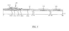
- FIG. 3 is a cross-sectional view of the TFT substrate along the A1-A1', B1-B1' and C-C' lines of FIG. 2 according to Embodiment 1 of the present invention.
- a gate electrode 1411 and a scan line 121 are firstly formed on the substrate 11, an insulating layer 1412 (also called as a gate insulating layer) is formed on the substrate 11, the gate electrode 1411 and the scan line 121, and then a semiconductor layer 1413 is formed on the gate electrode 1411.
- a source electrode 1414 and a drain electrode 1415 is formed on the semiconductor layer 1413, a data line 131 is simultaneously formed on the insulating layer 1412, and thus the data line 131, the scan line 121, and a first TFT unit 141 are obtained. Then, a protection layer 1416 and a pixel electrode 15 are sequentially laminated to obtain the TFT substrate of the present embodiment.
- the gate electrode 1411, the scan line 121, the source electrode 1414, the drain electrode 1415, and the data line 131 can be prepared with any conductive material generally used in the art, such as metals, alloys, metal oxides, metal oxynitrides, or other electrode materials generally used in the art.
- those units are prepared with metals, but the present invention is not limited thereto.
- the gate electrode 1411, the scan line 121, the source electrode 1414, the drain electrode 1415, and the data line 131 of the present embodiment are not limited to have a single layered structure prepared with only one material, and can have a composite structure with several laminated layers formed with different materials.
- the gate electrode 1411 and the scan line 121 respectively have a composite structure with a Ti layer and a Cu layer sequentially laminated from the side ofthe substrate 11; and the source electrode 1414, the drain electrode 1415, and the data line 131 respectively have a composite structure with a Mo layer, an A1 layer and another Mo layer sequentially laminated from the side of the substrate 11.
- the structures and the materials for the aforementioned units are not limited thereto.
- FIGs. 4A and 4B are respectively a cross-sectional view of a scan line on a thin film transistor substrate along the A1-A1' line and the A2-A2' line of FIG. 2 ; and FIGs. 5A and 5B are respectively a cross-sectional view of a data line on a thin film transistor substrate along the B1-B1' line and the B2-B2' line of FIG. 2 .
- the scan lines 121, 122 respectively electrically connect to the first TFT unit 141 and the second TFT unit 142, and are substantially arranged in parallel along a first direction Y.
- the scan lines 121, 122 respectively have an inclined surface 121', 122'.
- the data lines 131, 132 respectively electrically connect to the first TFT unit 141 and the second TFT unit 143, and are substantially arranged in parallel along a second direction X.
- the data lines 131, 132 respectively have an inclined surface 131', 132'.
- different scan lines 121, 122 have different thicknesses. More specifically, in the present embodiment, as shown in FIGs. 4A and 4B , the thickness M11 of the scan line 121 (the first thickness of the first conductive line) electrically connecting to the first TFT unit 141 is different from the thickness M12 of the scan line 122 (the third thickness of the second conductive line) electrically connecting to the second TFT unit 142.
- the thickness variation between M11 and M12 satisfy the equation:
- / M11 5-20%.
- different data lines 131, 132 have different thicknesses. More specifically, in the present embodiment, as shown in FIGs. 5A and 5B , the thickness M21 of the data line 131 (the second thickness of the second conductive line) electrically connecting to the first TFT unit 141 is different from the thickness M22 of the data line 132 (the fourth thickness of the fourth conductive line) electrically connecting to the second TFT unit 143.
- the thickness variation between M21 and M22 satisfy the equation:
- / M21 5-50%.
- the thickness variation between the thickness M21 of the data line 131 (the second thickness of the second conductive line) and the thickness M22 of the data line 132 (the fourth thickness of the fourth conductive line) is different from that between the thickness M11 of the scan line 121 (the first thickness of the first conductive line) and the thickness M12 of the scan line 122 (the third thickness of the third conductive line), which means that M11, M12, M21 and M22 satisfy the following equation (VI): M ⁇ 11 - M ⁇ 12
- the thickness variation between the thicknesses M21, M22 of the data lines 131 (the second thickness of the second conductive line) and the data line 132 (the fourth thickness of the fourth conductive line) is larger than that between the thicknesses M11, M12 of the scan line 121 (the first
- plural conductive lines such as the scan lines 121, 122 and the data lines 131, 132 are designed to have identical or different thicknesses.
- the increased widths of the conductive lines including the scan lines and the data lines can decrease resistance, but the increased widths thereof result in the reduced aperture ratio, which cannot meet the requirement for high PPI resolution.
- the thicknesses of the conductive lines are increased in the region with larger load during signal transmission to accomplish the purpose of reducing resistance to decrease the decay of the transmitted signals as well as to maintain high aperture ratio.
- the thicknesses M21, M22 of the data lines 131, 132 are larger than the thicknesses M11, M12 of the scan lines 121, 122.
- the increased widths of the scan lines can increase conductive area to reduce the resistance, but the increased widths of the data lines result in the aperture ratio decreased.
- the thicknesses of the data lines are increased to accomplish the purpose of reducing the width of the data lines to maintain high aperture ratio and prevent the transmitted signal decay.
- the thicknesses of partial scan lines are respectively 0.56 ⁇ m, 0.571 ⁇ m, 0.571 ⁇ m, 0.571 ⁇ m, 0.571 ⁇ m, 0.571 ⁇ m, 0.582 ⁇ m, 0.582 ⁇ m and 0.582 ⁇ m, in which the differences between the thicknesses of the aforementioned scan lines are located in a range from 0.01 ⁇ m to 0.02 ⁇ m.
- the thicknesses of partial data lines are respectively 0.615 ⁇ m, 0.681 ⁇ m, 0.637 ⁇ m, 0.593 ⁇ m, 0.626 ⁇ m, 0.626 ⁇ m, 0.648 ⁇ m, 0.692 ⁇ m and 0.659 ⁇ m, in which the differences between the thicknesses of the aforementioned data lines are located in a range from 0.02 ⁇ m to 0.1 ⁇ m.
- the thicknesses of the other scan lines and data lines in the display panel of the present embodiment are not limited to the aforementioned values, as long as the thicknesses thereof comply with the aforementioned requirements; and therefore the purpose of maintaining aperture ratio, reducing resistance, and reducing transmitted signal decay can be accomplished.
- the angles ⁇ 11 and ⁇ 12 included between the first surface 11' of the substrate 11 and the inclined surfaces 121', 122' of the scan lines 121, 122 are different from each other.
- the angle ⁇ 11 of the scan line 121 (the first angle of the first conductive line) electrically connected to the first TFT unit 141 is different from the angle ⁇ 12 of the scan line 122 (the third angle of the third conductive line) electrically connected to the first TFT unit 142.
- the angle variation between ⁇ 11 and ⁇ 12 satisfy the equation:
- / ⁇ 11 1-60%.
- the angles ⁇ 21 and ⁇ 22 included between the first surface 11' of the substrate 11 and the extension surfaces of the inclined surfaces 131', 132' of the data lines 131, 132 are different from each other.
- the angle ⁇ 21 included between the first surface 11' of the substrate 11 and the extension surface of the inclined surface 131' of the data line 131 and “the angle ⁇ 22 included between the first surface 11' of the first substrate 11 and the extension surface of the inclined surface 132' of the data line 132" are respectively called “the angle ⁇ 21” and "the angle ⁇ 22" for short.
- the angle ⁇ 21 of the data line 131 (the second angle of the second conductive line) electrically connected to the first TFT unit 141 is different from the angle ⁇ 22 of the data line 132 (the fourth angle of the fourth conductive line) electrically connected to the first TFT unit 143.
- the angle variation between ⁇ 21 and ⁇ 22 satisfy the equation:
- / ⁇ 21 5-20%.
- the angle variation between the angle ⁇ 21 of the data line 131 (the second angle of the second conductive line) and the angle ⁇ 22 of the data line 132 (the fourth angle of the fourth conductive line) is different from that between the angle ⁇ 11 of the scan line 121 (the first angle of the first conductive line) and the angle ⁇ 12 of the scan line 122 (the third angle of the third conductive line), which means ⁇ 11, ⁇ 12, ⁇ 21 and ⁇ 22 satisfy the following equation (III): ⁇ ⁇ 11 - ⁇ ⁇ 12 / ⁇ ⁇ 11 ⁇ ⁇ ⁇ 21 - ⁇ ⁇ 22 / ⁇ ⁇ 21
- the angle variation between the angles ⁇ 21, ⁇ 22 of the data line 131 (the second angle of the second conductive line) and the data line 132 (the fourth angle of the fourth conductive line) is smaller than that between the angles ⁇ 11,
- plural conductive lines such as the scan lines 121, 122 and the data lines 131, 132 are designed to have identical or different included angles.
- the thicknesses of the plural conductive lines can be varied as described above, the included angles thereof can also be varied to obtain different resistances when the thicknesses thereof cannot be easily controlled during the manufacturing process thereof.
- the angles ⁇ 21, ⁇ 22 of the data lines 131, 132 are designed to be larger than the angles ⁇ 11, ⁇ 12 of the scan lines 121, 122.
- the included angles of partial scan lines are respectively 30.96°, 34.99°, 21.91°, 42.84°, 20.72°, 40.76°, 36.25°, 47.34° and 40.56°, in which the differences between the angles of the aforementioned scan lines are located in a range from 1° to 26°.
- the included angles of partial data lines are respectively 64.3°, 69.4° and 77°, in which the differences between the angles of the aforementioned data lines are located in a range from 5° to 12°.
- angles of the other scan lines and data lines in the display panel of the present embodiment are not limited to the aforementioned values, as long as the angles thereof comply with the aforementioned requirements; and therefore the purpose of maintaining aperture ratio, reducing resistance, and reducing transmitted signal decay can be accomplished.
- the thicknesses and the angles of the data lines and the scan lines can be controlled through any conventional patterned process used in the art, such as the process by controlling the etching conditions, and the process with half-tone masks.
- the structure and the preparation process of the display panel of the present embodiment are the same as those illustrated in Embodiment 1, and the requirements for the thicknesses and the included angles of the scan lines and the data lines on the TFT substrate are also the same as those illustrated in Embodiment 1, except for the following differences.
- the gate electrode 1411, the scan line 121, the source electrode 1414, the drain electrode 1415, and the data line 131 respectively have a composite structure with a Ti layer and a Cu layer sequentially laminated from the side of the substrate 11.
- the structures and the materials for aforementioned units are not limited thereto.
- the thicknesses of partial scan lines are respectively 0.465 ⁇ m, 0.482 ⁇ m, 0.454 ⁇ m, 0.448 ⁇ m, 0.465 ⁇ m, 0.442 ⁇ m, 0.431 ⁇ m, 0.459 ⁇ m and 0.482 ⁇ m, in which the differences between the thicknesses of the aforementioned scan lines are located in a range from 0.01 ⁇ m to 0.05 ⁇ m.
- the thicknesses of partial data lines are respectively 0.478 ⁇ m, 0.469 ⁇ m, 0.496 ⁇ m, 0.532 ⁇ m, 0.514 ⁇ m, 0.496 ⁇ m, 0.487 ⁇ m, 0.46 ⁇ m and 0.469 ⁇ m, in which the differences between the thicknesses of the aforementioned data lines are located in a range from 0.01 ⁇ m to 0.07 ⁇ m.
- the thicknesses of the other scan lines and data lines in the display panel of the present embodiment are not limited to the aforementioned values
- the included angles of partial scan lines are respectively 34.42°, 27.8°, 24.83°, 27.76°, 19.83°, 25.46°, 18.25°, 40.79° and 27.51°, in which the differences between the angles of the aforementioned scan lines are located in a range from 2° to 22°.
- the included angles of partial data lines are respectively 65.56°, 56.73°, 60.95°, 62.1°, 61.26°, 55.92°, 60.26°, 60.8 and 54.16°, in which the differences between the angles of the aforementioned data lines are located in a range from 2° to 11°.
- the angles of the other scan lines and data lines in the display panel of the present embodiment are not limited to the aforementioned values.
- Embodiments 1 and 2 only the liquid crystal panels assembled with the conventional TFT substrate and the CF substrate are illustrated.
- other display panels known in the art such as color on array (COA) display panels, organic light emitting diode (OLED) display panels, plasma display panels and the like can equipped with the aforementioned TFT substrates as illustrated in Embodiments 1 and 2 to accomplish the purpose of maintaining aperture ratio, reducing resistance, and reducing transmitted signal decay can be accomplished.
- COA color on array
- OLED organic light emitting diode
- plasma display panels and the like can equipped with the aforementioned TFT substrates as illustrated in Embodiments 1 and 2 to accomplish the purpose of maintaining aperture ratio, reducing resistance, and reducing transmitted signal decay can be accomplished.
- the display panel provided by the present invention can be applied to any electronic devices such as a mobile phone, a notebook, a camera, a video camera, a music player, a navigation system, or a television.
Landscapes
- Physics & Mathematics (AREA)
- Nonlinear Science (AREA)
- Mathematical Physics (AREA)
- Chemical & Material Sciences (AREA)
- Crystallography & Structural Chemistry (AREA)
- General Physics & Mathematics (AREA)
- Optics & Photonics (AREA)
- Engineering & Computer Science (AREA)
- Microelectronics & Electronic Packaging (AREA)
- Devices For Indicating Variable Information By Combining Individual Elements (AREA)
- Liquid Crystal (AREA)
Abstract
A display panel is disclosed, which comprises: a substrate (11) with a first surface (11'), a first thin film transistor unit (141) and a second thin film transistor unit (142) disposed on the first surface (11') of the substrate (11); a conductive scan line (121) with a first inclined surface (121') disposed on the first surface (11') of the substrate (11) and electrically connected to the first thin film transistor unit (141); a conductive data line (131) with a second inclined surface (131') disposed on the first surface (11') of the substrate (11) and electrically connected to the second thin film transistor unit (142), wherein the angle (theta11) included between the first surface (11') and the first inclined surface (121') or an extension thereof defines a first angle (theta11), the angle (theta21) included between the first surface (11') and the second inclined surface (131') or an extension thereof defines a second angle (theta21), and the first angle (theta11) is different from the second angle (theta21).
Description
- This application claims the benefits of the Taiwan Patent Application Serial Number
103111664, filed on March 28, 2014 - The present invention relates to a display panel and, more particularly, to a display panel in which the decay of transmitted signals in circuits can be reduced.
- As the techniques of display panel progress, the demands for the commercial display panels with high resolutions increase. Hence, many manufacturers actively developed high-level display panels. In particular, as the developments of 4K2K panels and mobile devices such as mobile phones and tablets with high PPI (pixels per inch), the display panels with more pixels in per unit area is the trend for the next generation.
- However, in order to meet the requirement for high PPI, the currently used conductive lines including scan lines or data lines with identical widths may cause aperture ratio decreased. Hence, reducing the widths of the conductive lines is one means to accomplish the demand for high PPI and high aperture ratio. However, when the widths of the conductive lines are too small, the small conductive lines may be peeled off during the manufacturing process, and the resistance thereof may be increased, resulting in the decay of the transmitted signals.
- Therefore, it is desirable to provide a display panel without the aforementioned problems to apply to the display panel with high PPI.
- An object of the present invention is to provide a display panel, in which the resistance and the decay of transmitted signals in circuits can be reduced by adjusting the thickness or the profile of conductive lines in a display region of the display panel.
- To achieve the object, the display panel of the present invention comprises: a substrate with a first surface; a first thin film transistor unit and a second thin film transistor unit respectively disposed on the first surface of the substrate; a first conductive line with a first inclined surface, disposed on the first surface of the substrate and electrically connecting to the first thin film transistor unit; and a second conductive line with a second inclined surface, disposed on the first surface of the substrate and electrically connecting to the second thin film transistor unit, wherein an angle included between the first surface and the first inclined surface or an extension surface thereof of the first conductive line is defined as a first angle, an angle included between the first surface and the second inclined surface or an extension thereof of the second conductive line is defined as a second angle, and the first angle is different from the second angle.
- Herein, the first conductive line and the second conductively can respectively a scan line or a data line. In one aspect of the present invention, the first conductive line may be a scan line, and the second conductive line may be a data line. In this case, the second angle is larger than the first angle.
- In addition, the display panel of the present invention may further comprise: a third conductive line and a fourth conductive line respectively disposed on the first surface of the substrate and respectively comprising a third inclined surface and a fourth inclined surface, wherein the first conductive line and the third conductive line are respectively disposed along a first direction, the second conductive line and the fourth conductive line are respectively disposed along a second direction, the first direction intersects the second direction, an angle included between the first surface and the third inclined surface or an extension surface thereof of the third conductive line is defined as a third angle, an angle included between the first surface and the fourth inclined surface or an extension surface thereof of the fourth conductive line is defined as a fourth angle, and the first angle is different from the third angle or the fourth angle. Herein the first conductive line and the third conductive line may be respectively a scan line, and the second conductive line and the fourth conductive line may be respectively a data line. In this case, an angle variation between the second angle and the fourth angle is smaller than that between the first angle and the third angle.
- In the display panel of the present invention, each the first conductive line, the second conductive line, the third conductive line and the fourth conductive line can be respectively a scan line or a data line. In one aspect of the present invention, the first conductive line and the third conductive line are respectively the scan lines, and the second conductive line and the fourth conductive line are respectively the data lines.
- In one aspect of the present invention, the first angle and the third angle respectively are θ11 and θ12, which satisfy the following equation (I):

- In addition, the second angle and the fourth angle respectively are θ21 and θ22, which satisfy the following equation (II):

- Furthermore, θ11, θ12, θ21 and θ22 satisfy the following equation (III):

- The present invention further provides another display panel, comprising: a substrate; a first thin film transistor unit and a second thin film transistor unit respectively disposed on the substrate; a first conductive line disposed on the substrate and electrically connecting to the first thin film transistor unit; and a second conductive line disposed on the substrate and electrically connecting to the second thin film transistor unit, wherein a thickness of the first conductive line is defined as a first thickness, a thickness of the second conductive line is defined as a second thickness, and the first thickness is different from the second thickness.
- Herein, the first conductive line and the second conductively can respectively a scan line or a data line. In one aspect of the present invention, the first conductive line may be a scan line, and the second conductive line may be a data line. In this case, the second thickness is larger than the first thickness.
- In addition, the display panel of the present invention may further comprise: a third conductive line and a fourth conductive line respectively disposed on the substrate, wherein the first conductive line and the third conductive line are respectively disposed along a first direction, the second conductive line and the fourth conductive line are respectively disposed along a second direction, the first direction intersects the second direction, a thickness of the third conductive line is defined as a third thickness, a thickness of the fourth conductive line is defined as a fourth thickness, and the first thickness is different from the third thickness or the fourth thickness. Herein, the first conductive line and the third conductive line are respectively the scan lines, and the second conductive line and the fourth conductive line are respectively the data lines. In this case, a thickness variation between the second thickness and the fourth thickness is larger than that between the first thickness and the third thickness.
- In the display panel of the present invention, each the first conductive line, the second conductive line, the third conductive line and the fourth conductive line can be respectively a scan line or a data line. In one aspect of the present invention, the first conductive line and the third conductive line are respectively the scan lines, and the second conductive line and the fourth conductive line are respectively the data lines.
- In one aspect of the present invention, the first thickness and the third thickness respectively are M11 and M12, which satisfy the following equation (IV):

- In addition, the second thickness and the fourth thickness respectively are M21 and M22, which satisfy the following equation (V):

- Furthermore, M11, M12, M21 and M22 satisfy the following equation (VI):

- The present invention further provides a display panel, in which the thicknesses of the conductive lines and the angles included between the first surface of the substrate and the inclined surfaces or the extensions thereof of the conductive lines simultaneously satisfy the aforementioned features.
- In the present invention, the term "inclined surface" indicates a side surface connecting to an upper surface and a bottom surface of the conductive line, in which the upper surface and the bottom surface thereof are substantially parallel to the first surface of the substrate. In addition, in the present invention, both the terms "thickness" and "angle included between a first surface and an inclined surface or an extension thereof" indicate the thickness and the angle included between the first surface and the inclined surface or the extension thereof of a cross-section of the conductive line, in which the cross-section is a cross-section vertical to a length direction of the conductive line.
- Other objects, advantages, and novel features of the invention will become more apparent from the following detailed description when taken in conjunction with the accompanying drawings.
-
-
FIG. 1 is a perspective view of a liquid display panel according to Embodiment 1 of the present invention; -
FIG. 2 is a perspective view of a thin film transistor substrate according to Embodiment 1 of the present invention; -
FIG. 3 is a cross-sectional view of a thin film transistor substrate according to Embodiment 1 of the present invention; -
FIG. 4A is a cross-sectional view of a scan line on a thin film transistor substrate along the A1-A1' line ofFIG. 2 according to Embodiment 1 of the present invention; -
FIG. 4B is a cross-sectional view of a scan line on a thin film transistor substrate along the A2-A2' line ofFIG. 2 according to Embodiment 1 of the present invention; -
FIG. 5A is a cross-sectional view of a data line on a thin film transistor substrate along the B1-B1' line ofFIG. 2 according to Embodiment 1 of the present invention; and -
FIG. 5B is a cross-sectional view of a data line on a thin film transistor substrate along the B2-B2' line ofFIG. 2 according to Embodiment 1 of the present invention. - The present invention has been described in an illustrative manner, and it is to be understood that the terminology used is intended to be in the nature of description rather than of limitation. Many modifications and variations of the present invention are possible in light of the above teachings. Therefore, it is to be understood that within the scope of the appended claims, the invention may be practiced otherwise than as specifically described.
-
FIG. 1 is a perspective view of a liquid display panel of the present embodiment. The display panel of the present embodiment comprises: a thin film transistor (TFT) substrate 1, a color filter (CF)substrate 2,plural spacers 3, aliquid crystal layer 4 and a sealant 5. Herein, the TFT substrate 1 and theCF substrate 2 are opposite to each other, thespacers 3 and theliquid crystal layer 4 are disposed therebetween, and the TFT substrate 1 and theCF substrate 2 are assembled to each other with the sealant 5. Hereinafter, detail structures of units disposed on the TFT substrate 1 of the liquid display panel of the present embodiment are illustrated below. -
FIG. 2 is a perspective view of the TFT substrate of the present embodiment. The TFT substrate of the present embodiment comprises: a first substrate (not shown in the figure), wherein plural conductive lines includingscan lines data lines unit 141,second TFT units pixel electrode 15 and acapacitor electrode 17 are disposed thereon. Herein, twoadjacent scan lines adjacent data lines pixel electrode 15 and acapacitor electrode 17, and thepixel electrode 15 is located between twoadjacent scan lines adjacent data lines scan lines data lines -
FIG. 3 is a cross-sectional view of the TFT substrate along the A1-A1', B1-B1' and C-C' lines ofFIG. 2 according to Embodiment 1 of the present invention. Herein, only thefirst TFT unit 141 is exemplified, and the other TFT units can be manufactured through the same process. During the manufacturing process for the TFT substrate of the present embodiment, agate electrode 1411 and ascan line 121 are firstly formed on thesubstrate 11, an insulating layer 1412 (also called as a gate insulating layer) is formed on thesubstrate 11, thegate electrode 1411 and thescan line 121, and then asemiconductor layer 1413 is formed on thegate electrode 1411. Next, asource electrode 1414 and adrain electrode 1415 is formed on thesemiconductor layer 1413, adata line 131 is simultaneously formed on the insulatinglayer 1412, and thus thedata line 131, thescan line 121, and afirst TFT unit 141 are obtained. Then, aprotection layer 1416 and apixel electrode 15 are sequentially laminated to obtain the TFT substrate of the present embodiment. Herein, thegate electrode 1411, thescan line 121, thesource electrode 1414, thedrain electrode 1415, and thedata line 131 can be prepared with any conductive material generally used in the art, such as metals, alloys, metal oxides, metal oxynitrides, or other electrode materials generally used in the art. Preferably, those units are prepared with metals, but the present invention is not limited thereto. Thegate electrode 1411, thescan line 121, thesource electrode 1414, thedrain electrode 1415, and thedata line 131 of the present embodiment are not limited to have a single layered structure prepared with only one material, and can have a composite structure with several laminated layers formed with different materials. In the present embodiment, thegate electrode 1411 and thescan line 121 respectively have a composite structure with a Ti layer and a Cu layer sequentially laminated from the side ofthesubstrate 11; and thesource electrode 1414, thedrain electrode 1415, and thedata line 131 respectively have a composite structure with a Mo layer, an A1 layer and another Mo layer sequentially laminated from the side of thesubstrate 11. However, in other embodiment, the structures and the materials for the aforementioned units are not limited thereto. -
FIGs. 4A and 4B are respectively a cross-sectional view of a scan line on a thin film transistor substrate along the A1-A1' line and the A2-A2' line ofFIG. 2 ; andFIGs. 5A and 5B are respectively a cross-sectional view of a data line on a thin film transistor substrate along the B1-B1' line and the B2-B2' line ofFIG. 2 . In order to describe the designs of the data lines and the scan lines, other units disposed thereon are not shown in the figures. As shown inFIG. 2 , thescan lines first TFT unit 141 and thesecond TFT unit 142, and are substantially arranged in parallel along a first direction Y. Also, as shown inFIGs. 4A and 4B , thescan lines FIG. 2 , thedata lines first TFT unit 141 and thesecond TFT unit 143, and are substantially arranged in parallel along a second direction X. Also, as shown inFIGs. 5A and 5B , thedata lines - In the present embodiment, as shown in
FIGs. 2 ,4A and 4B ,different scan lines FIGs. 4A and 4B , the thickness M11 of the scan line 121 (the first thickness of the first conductive line) electrically connecting to thefirst TFT unit 141 is different from the thickness M12 of the scan line 122 (the third thickness of the second conductive line) electrically connecting to thesecond TFT unit 142. Preferably, the thickness variation between M11 and M12 satisfy the equation: |M11-M12| / M11 = 5-20%. - In addition, in the present embodiment, as shown in
FIGs. 2 ,5A and 5B ,different data lines FIGs. 5A and 5B , the thickness M21 of the data line 131 (the second thickness of the second conductive line) electrically connecting to thefirst TFT unit 141 is different from the thickness M22 of the data line 132 (the fourth thickness of the fourth conductive line) electrically connecting to thesecond TFT unit 143. Preferably, the thickness variation between M21 and M22 satisfy the equation: |M21-M22| / M21 = 5-50%. - Furthermore, in the present embodiment, as shown in
FIGs. 2 ,4A, 4B, 5A and 5B , the thickness variation between the thickness M21 of the data line 131 (the second thickness of the second conductive line) and the thickness M22 of the data line 132 (the fourth thickness of the fourth conductive line) is different from that between the thickness M11 of the scan line 121 (the first thickness of the first conductive line) and the thickness M12 of the scan line 122 (the third thickness of the third conductive line), which means that M11, M12, M21 and M22 satisfy the following equation (VI):
Preferably, the thickness variation between the thicknesses M21, M22 of the data lines 131 (the second thickness of the second conductive line) and the data line 132 (the fourth thickness of the fourth conductive line) is larger than that between the thicknesses M11, M12 of the scan line 121 (the first thickness of the first conductive line) and the scan line 122 (the third thickness of the third conductive line), i.e. |M11-M12| / M11 < |M21-M22| / M21. - In the present embodiment, as shown in
FIGs. 2 ,4A, 4B, 5A and 5B , plural conductive lines such as thescan lines data lines data lines scan lines - In the display panel of the present embodiment, the thicknesses of partial scan lines are respectively 0.56 µm, 0.571 µm, 0.571 µm, 0.571 µm, 0.571 µm, 0.571 µm, 0.582 µm, 0.582 µm and 0.582 µm, in which the differences between the thicknesses of the aforementioned scan lines are located in a range from 0.01 µm to 0.02 µm. In addition, the thicknesses of partial data lines are respectively 0.615 µm, 0.681 µm, 0.637 µm, 0.593 µm, 0.626 µm, 0.626 µm, 0.648 µm, 0.692 µm and 0.659 µm, in which the differences between the thicknesses of the aforementioned data lines are located in a range from 0.02 µm to 0.1 µm. However, the thicknesses of the other scan lines and data lines in the display panel of the present embodiment are not limited to the aforementioned values, as long as the thicknesses thereof comply with the aforementioned requirements; and therefore the purpose of maintaining aperture ratio, reducing resistance, and reducing transmitted signal decay can be accomplished.
- Furthermore, in the present embodiment, as shown in
FIGs. 2 ,4A and 4B , the angles θ11 and θ12 included between the first surface 11' of thesubstrate 11 and the inclined surfaces 121', 122' of thescan lines substrate 11 and theinclined surface 121 of thescans line 121" and "the angle θ12 included between the first surface 11' of thesubstrate 11 and the inclined surface 122' of thescans line 122" are respectively called "the angle θ11" and "the angle θ12" for short. More specifically, in the present embodiment, the angle θ11 of the scan line 121 (the first angle of the first conductive line) electrically connected to thefirst TFT unit 141 is different from the angle θ12 of the scan line 122 (the third angle of the third conductive line) electrically connected to thefirst TFT unit 142. Preferably, the angle variation between θ11 and θ12 satisfy the equation: |θ11-θ12| /θ11 = 1-60%. - In addition, in the present embodiment, as shown in
FIGs. 2 ,5A and 5B , the angles θ21 and θ22 included between the first surface 11' of thesubstrate 11 and the extension surfaces of the inclined surfaces 131', 132' of thedata lines substrate 11 and the extension surface of the inclined surface 131' of thedata line 131" and "the angle θ22 included between the first surface 11' of thefirst substrate 11 and the extension surface of the inclined surface 132' of thedata line 132" are respectively called "the angle θ21" and "the angle θ22" for short. More specifically, in the present embodiment, the angle θ21 of the data line 131 (the second angle of the second conductive line) electrically connected to thefirst TFT unit 141 is different from the angle θ22 of the data line 132 (the fourth angle of the fourth conductive line) electrically connected to thefirst TFT unit 143. Preferably, the angle variation between θ21 and θ22 satisfy the equation: |θ21-θ22| / θ21 = 5-20%. - Furthermore, in the present embodiment, as shown in
FIGs. 2 ,4A, 4B, 5A and 5B , the angle variation between the angle θ21 of the data line 131 (the second angle of the second conductive line) and the angle θ22 of the data line 132 (the fourth angle of the fourth conductive line) is different from that between the angle θ11 of the scan line 121 (the first angle of the first conductive line) and the angle θ12 of the scan line 122 (the third angle of the third conductive line), which meansθ11, θ12, θ21 and θ22 satisfy the following equation (III):
Preferably, the angle variation between the angles θ21, θ22 of the data line 131 (the second angle of the second conductive line) and the data line 132 (the fourth angle of the fourth conductive line) is smaller than that between the angles θ11, θ12 of the scan line 121 (the first angle of the first conductive line) and the scan line 122 (the third angle of the third conductive line), i.e. |θ11-θ12| / θ11 > |θ21-θ22| / θ21. - In the present embodiment, as shown in
FIGs. 2 ,4A, 4B, 5A and 5B , plural conductive lines such as thescan lines data lines data lines scan lines data lines scan lines - In the display panel of the present invention, the included angles of partial scan lines are respectively 30.96°, 34.99°, 21.91°, 42.84°, 20.72°, 40.76°, 36.25°, 47.34° and 40.56°, in which the differences between the angles of the aforementioned scan lines are located in a range from 1° to 26°. In addition, the included angles of partial data lines are respectively 64.3°, 69.4° and 77°, in which the differences between the angles of the aforementioned data lines are located in a range from 5° to 12°. However, the angles of the other scan lines and data lines in the display panel of the present embodiment are not limited to the aforementioned values, as long as the angles thereof comply with the aforementioned requirements; and therefore the purpose of maintaining aperture ratio, reducing resistance, and reducing transmitted signal decay can be accomplished.
- In the present invention, the thicknesses and the angles of the data lines and the scan lines can be controlled through any conventional patterned process used in the art, such as the process by controlling the etching conditions, and the process with half-tone masks.
- The structure and the preparation process of the display panel of the present embodiment are the same as those illustrated in Embodiment 1, and the requirements for the thicknesses and the included angles of the scan lines and the data lines on the TFT substrate are also the same as those illustrated in Embodiment 1, except for the following differences.
- In the present embodiment, the
gate electrode 1411, thescan line 121, thesource electrode 1414, thedrain electrode 1415, and thedata line 131 respectively have a composite structure with a Ti layer and a Cu layer sequentially laminated from the side of thesubstrate 11. However, in other embodiment of the present invention, the structures and the materials for aforementioned units are not limited thereto. - In addition, in the display panel of the present embodiment, the thicknesses of partial scan lines are respectively 0.465 µm, 0.482 µm, 0.454 µm, 0.448 µm, 0.465 µm, 0.442 µm, 0.431 µm, 0.459 µm and 0.482 µm, in which the differences between the thicknesses of the aforementioned scan lines are located in a range from 0.01 µm to 0.05 µm. In addition, the thicknesses of partial data lines are respectively 0.478 µm, 0.469 µm, 0.496 µm, 0.532 µm, 0.514 µm, 0.496 µm, 0.487 µm, 0.46 µm and 0.469 µm, in which the differences between the thicknesses of the aforementioned data lines are located in a range from 0.01 µm to 0.07 µm. However, the thicknesses of the other scan lines and data lines in the display panel of the present embodiment are not limited to the aforementioned values
- Furthermore, in the display panel of the present embodiment, the included angles of partial scan lines are respectively 34.42°, 27.8°, 24.83°, 27.76°, 19.83°, 25.46°, 18.25°, 40.79° and 27.51°, in which the differences between the angles of the aforementioned scan lines are located in a range from 2° to 22°. In addition, the included angles of partial data lines are respectively 65.56°, 56.73°, 60.95°, 62.1°, 61.26°, 55.92°, 60.26°, 60.8 and 54.16°, in which the differences between the angles of the aforementioned data lines are located in a range from 2° to 11°. However, the angles of the other scan lines and data lines in the display panel of the present embodiment are not limited to the aforementioned values.
- In the aforementioned Embodiments 1 and 2, only the liquid crystal panels assembled with the conventional TFT substrate and the CF substrate are illustrated. However, other display panels known in the art such as color on array (COA) display panels, organic light emitting diode (OLED) display panels, plasma display panels and the like can equipped with the aforementioned TFT substrates as illustrated in
Embodiments 1 and 2 to accomplish the purpose of maintaining aperture ratio, reducing resistance, and reducing transmitted signal decay can be accomplished. - Furthermore, the display panel provided by the present invention can be applied to any electronic devices such as a mobile phone, a notebook, a camera, a video camera, a music player, a navigation system, or a television.
- Although the present invention has been explained in relation to its preferred embodiment, it is to be understood that many other possible modifications and variations can be made without departing from the spirit and scope of the invention as hereinafter claimed.
Claims (15)
- A display panel, comprising:a substrate (11) with a first surface (11');a first thin film transistor unit (141) and a second thin film transistor unit (142) respectively disposed on the first surface of the substrate;a first conductive line (121) with a first inclined surface (121'), disposed on the first surface (11') of the substrate and electrically connecting to the first thin film transistor unit (141); anda second conductive line (131) with a second inclined surface (122'), disposed on the first surface (11') of the substrate and electrically connecting to the second thin film transistor unit (142),wherein an angle (θ11) included between the first surface (11') and the first inclined surface (121') or an extension surface thereof of the first conductive line is defined as a first angle, an angle (θ21) included between the first surface (11') and the second inclined surface (122') or an extension thereof of the second conductive line is defined as a second angle, and the first angle (θ11) is different from the second angle (θ21).
- The display panel as claimed in claim 1, wherein the first conductive line is a scan line (121), and the second conductive line is a data line (131).
- The display panel as claimed in claim 2, wherein the second angle is greater than the first angle.
- The display panel as claimed in one of the preceding claims, further comprising:a third conductive line (122) and a fourth conductive line (132) respectively disposed on the first surface of the substrate and respectively comprising a third inclined surface and a fourth inclined surface,wherein the first conductive line and the third conductive line are respectively disposed along a first direction, the second conductive line and the fourth conductive line are respectively disposed along a second direction, the first direction intersects the second direction,an angle (θ12) included between the first surface and the third inclined surface or an extension surface thereof of the third conductive line is defined as a third angle,an angle (θ22) included between the first surface and the fourth inclined surface or an extension surface thereof of the fourth conductive line is defined as a fourth angle, and the first angle is different from the third angle or the fourth angle.
- The display panel as claimed in claim 4, wherein an angle variation between the second angle and the fourth angle is smaller than that between the first angle and the third angle.
- The display panel as claimed in claim 4, wherein the first angle and the third angle respectively are θ11 and θ12, which satisfy the following equation (I): |θ11-θ12| / θ11 = 1-60% (I).
- The display panel as claimed in claim 4, wherein the second angle and the fourth angle respectively are θ21 and θ22, which satisfy the following equation (II):

- The display panel as claimed in one of the preceding claims, wherein a thickness of the first conductive line is different from that of the second conductive line.
- A display panel, comprising:a substrate;a first thin film transistor unit and a second thin film transistor unit respectively disposed on the substrate;a first conductive line disposed on the substrate and electrically connecting to the first thin film transistor unit; anda second conductive line disposed on the substrate and electrically connecting to the second thin film transistor unit,wherein a thickness of the first conductive line is defined as a first thickness, a thickness of the second conductive line is defined as a second thickness, and the first thickness is different from the second thickness.
- The display panel as claimed in claim 9, wherein the first conductive line is a scan line, and the second conductive line is a data line.
- The display panel as claimed in claim 10, wherein the second thickness is larger than the first thickness.
- The display panel as claimed in one of the claims 9 to 11, further comprising: a third conductive line and a fourth conductive line respectively disposed on the substrate, wherein the first conductive line and the third conductive line are respectively disposed along a first direction, the second conductive line and the fourth conductive line are respectively disposed along a second direction, the first direction intersects the second direction, a thickness of the third conductive line is defined as a third thickness, a thickness of the fourth conductive line is defined as a fourth thickness, and the first thicknesses is different from the third thickness or the fourth thickness.
- The display panel as claimed in claim 12, wherein a thickness variation between the second thicknesses and the fourth thickness is larger than that between the first thicknesses and the third thickness.
- The display panel as claimed in claim 12, wherein the first thicknesses and the third thickness respectively are M11 and M12, which satisfy the following equation (IV):

- The display panel as claimed in claim 12, wherein the second thicknesses and the fourth thickness respectively are M21 and M22, which satisfy the following equation (V):

Applications Claiming Priority (1)
| Application Number | Priority Date | Filing Date | Title |
|---|---|---|---|
| TW103111664A TWI528074B (en) | 2014-03-28 | 2014-03-28 | Display panel |
Publications (1)
| Publication Number | Publication Date |
|---|---|
| EP2924499A1 true EP2924499A1 (en) | 2015-09-30 |
Family
ID=50842194
Family Applications (1)
| Application Number | Title | Priority Date | Filing Date |
|---|---|---|---|
| EP14171152.3A Withdrawn EP2924499A1 (en) | 2014-03-28 | 2014-06-04 | High aperture ratio display panel with adjusted thickness and profile of its scan and data lines |
Country Status (6)
| Country | Link |
|---|---|
| US (2) | US9620528B2 (en) |
| EP (1) | EP2924499A1 (en) |
| JP (1) | JP3196528U (en) |
| KR (1) | KR20150112748A (en) |
| CN (2) | CN110068971B (en) |
| TW (1) | TWI528074B (en) |
Families Citing this family (4)
| Publication number | Priority date | Publication date | Assignee | Title |
|---|---|---|---|---|
| TWI528074B (en) | 2014-03-28 | 2016-04-01 | 群創光電股份有限公司 | Display panel |
| CN105807524B (en) * | 2016-05-30 | 2019-04-16 | 京东方科技集团股份有限公司 | Array substrate, display panel and display device |
| CN208637462U (en) * | 2018-08-29 | 2019-03-22 | 京东方科技集团股份有限公司 | A kind of encapsulating structure of display device, display device |
| CN111583849A (en) * | 2020-05-19 | 2020-08-25 | 深圳市华星光电半导体显示技术有限公司 | Display panel and display device |
Citations (2)
| Publication number | Priority date | Publication date | Assignee | Title |
|---|---|---|---|---|
| JPH1090702A (en) * | 1996-09-18 | 1998-04-10 | Toshiba Corp | Liquid crystal display |
| US20010040648A1 (en) * | 2000-05-12 | 2001-11-15 | Hitachi Ltd. | Liquid crystal display device and fabrication method thereof |
Family Cites Families (27)
| Publication number | Priority date | Publication date | Assignee | Title |
|---|---|---|---|---|
| US5663525A (en) | 1995-03-20 | 1997-09-02 | Newman; James R. | Electrical meter box for service lateral and method of using same |
| US6008874A (en) * | 1995-03-27 | 1999-12-28 | Sanyo Electric Co., Ltd. | Active matrix liquid crystal display having alignment film with inclined surface |
| US6208394B1 (en) * | 1997-11-27 | 2001-03-27 | Sharp Kabushiki Kaisha | LCD device and method for fabricating the same having color filters and a resinous insulating black matrix on opposite sides of a counter electrode on the same substrate |
| JP4627843B2 (en) * | 1999-07-22 | 2011-02-09 | 株式会社半導体エネルギー研究所 | Semiconductor device |
| KR100798761B1 (en) * | 1999-09-07 | 2008-01-29 | 가부시키가이샤 히타치세이사쿠쇼 | LCD Display |
| US7023021B2 (en) * | 2000-02-22 | 2006-04-04 | Semiconductor Energy Laboratory Co., Ltd. | Semiconductor device and method of manufacturing the same |
| US6580475B2 (en) * | 2000-04-27 | 2003-06-17 | Semiconductor Energy Laboratory Co., Ltd. | Semiconductor device and method of fabricating the same |
| JP3750055B2 (en) * | 2001-02-28 | 2006-03-01 | 株式会社日立製作所 | Liquid crystal display |
| KR100404161B1 (en) * | 2001-05-03 | 2003-11-03 | 엘지.필립스 엘시디 주식회사 | Transmissive Liquid Crystal Display Device having Hologram Diffuser |
| JP2005164854A (en) * | 2003-12-01 | 2005-06-23 | Nec Lcd Technologies Ltd | Liquid crystal display |
| JP2006293343A (en) * | 2005-03-17 | 2006-10-26 | Hitachi Displays Ltd | Liquid crystal display device and display device |
| US7595506B2 (en) * | 2005-03-17 | 2009-09-29 | Hitachi Displays, Ltd. | Liquid crystal display device and display device |
| JP4702067B2 (en) * | 2006-01-16 | 2011-06-15 | セイコーエプソン株式会社 | ELECTRO-OPTICAL DEVICE, ELECTRONIC DEVICE, AND PROJECTOR |
| TWI381230B (en) * | 2008-01-31 | 2013-01-01 | Hannstar Display Corp | Pixel structure of liquid crystal display |
| CN101232029B (en) * | 2008-02-25 | 2014-02-05 | 友达光电股份有限公司 | Liquid crystal display panel and semiconductor array basal plate |
| KR101479998B1 (en) * | 2008-08-12 | 2015-01-09 | 삼성디스플레이 주식회사 | Thin film transistor display panel and manufacturing method thereof |
| KR101448000B1 (en) * | 2008-08-26 | 2014-10-14 | 삼성디스플레이 주식회사 | Thin film transistor substrate and manufacturing method thereof |
| KR20100078433A (en) | 2008-12-30 | 2010-07-08 | 주식회사 동부하이텍 | Modeling structure for simulation of trapezoidal metal line |
| KR101595818B1 (en) * | 2009-08-26 | 2016-02-22 | 삼성디스플레이 주식회사 | Thin film transistor array panel and manufacturing the same |
| KR101628989B1 (en) * | 2009-09-07 | 2016-06-10 | 삼성디스플레이 주식회사 | Liquid crystal display and fabrication method of the same |
| TWI400540B (en) * | 2009-09-11 | 2013-07-01 | 瀚宇彩晶股份有限公司 | Pixel structure of liquid crystal display panel |
| US8270178B2 (en) * | 2010-03-22 | 2012-09-18 | Au Optronics Corporation | Active device array substrate |
| WO2013011602A1 (en) | 2011-07-19 | 2013-01-24 | パナソニック株式会社 | Display device and method for manufacturing display device |
| KR101914168B1 (en) * | 2011-08-10 | 2018-11-02 | 삼성디스플레이 주식회사 | Display substrate and method of manufacturing thereof |
| CN102709241A (en) | 2012-05-11 | 2012-10-03 | 北京京东方光电科技有限公司 | Thin film transistor array substrate and preparation method and display device |
| CN103454818A (en) * | 2012-05-30 | 2013-12-18 | 群康科技(深圳)有限公司 | Conductive structure applied to panel and manufacturing method of conductive structure |
| TWI528074B (en) | 2014-03-28 | 2016-04-01 | 群創光電股份有限公司 | Display panel |
-
2014
- 2014-03-28 TW TW103111664A patent/TWI528074B/en active
- 2014-06-04 EP EP14171152.3A patent/EP2924499A1/en not_active Withdrawn
- 2014-11-19 CN CN201910110929.2A patent/CN110068971B/en active Active
- 2014-11-19 CN CN201410664896.3A patent/CN104952878B/en active Active
- 2014-12-15 US US14/571,258 patent/US9620528B2/en active Active
- 2014-12-24 JP JP2014006805U patent/JP3196528U/en not_active Expired - Lifetime
- 2014-12-29 KR KR1020140191851A patent/KR20150112748A/en not_active Ceased
-
2017
- 2017-02-27 US US15/444,014 patent/US10211234B2/en active Active
Patent Citations (2)
| Publication number | Priority date | Publication date | Assignee | Title |
|---|---|---|---|---|
| JPH1090702A (en) * | 1996-09-18 | 1998-04-10 | Toshiba Corp | Liquid crystal display |
| US20010040648A1 (en) * | 2000-05-12 | 2001-11-15 | Hitachi Ltd. | Liquid crystal display device and fabrication method thereof |
Also Published As
| Publication number | Publication date |
|---|---|
| JP3196528U (en) | 2015-03-19 |
| CN104952878A (en) | 2015-09-30 |
| TWI528074B (en) | 2016-04-01 |
| US10211234B2 (en) | 2019-02-19 |
| US9620528B2 (en) | 2017-04-11 |
| US20170170201A1 (en) | 2017-06-15 |
| CN110068971A (en) | 2019-07-30 |
| KR20150112748A (en) | 2015-10-07 |
| TW201537261A (en) | 2015-10-01 |
| CN104952878B (en) | 2019-03-08 |
| CN110068971B (en) | 2022-09-20 |
| US20150279858A1 (en) | 2015-10-01 |
Similar Documents
| Publication | Publication Date | Title |
|---|---|---|
| US9329444B2 (en) | Liquid crystal display device | |
| CN105655391B (en) | Tft array substrate and preparation method thereof | |
| CN109585458B (en) | Thin film transistor substrate | |
| US9897877B2 (en) | Thin film transistor array substrate and liquid crystal display panel using same | |
| US11036322B2 (en) | Array substrate and method of manufacturing same | |
| WO2016086539A1 (en) | Liquid crystal panel and manufacturing method therefor | |
| US10211234B2 (en) | Display panel | |
| US20170110478A1 (en) | Array substrate, electro-static discharge method thereof and display device | |
| KR20120107269A (en) | Liquid crystal display device and method for fabricating the same | |
| US20160202564A1 (en) | Display device | |
| US20110254006A1 (en) | Display device and manufacturing method thereof | |
| US20100259715A1 (en) | Active matrix substrate, method for manufacturing same, and liquid crystal display apparatus | |
| US9923067B2 (en) | Thin-film transistor and method for fabricating the same, array substrate and method for fabricating the same, and display device | |
| US7053977B2 (en) | Laser repair structure of liquid crystal display device and method thereof | |
| CN103985671A (en) | Array substrate manufacturing method, array substrate and display device | |
| US20200365106A1 (en) | Bootstrap capacitor of gate driver on array circuit, gate driver on array circuit and display panel | |
| US7800704B2 (en) | Liquid crystal display comprising intersecting common lines | |
| US7514713B2 (en) | Liquid crystal display panel | |
| JP4757550B2 (en) | Display device and manufacturing method thereof | |
| US20170343875A1 (en) | Display device | |
| TWI522716B (en) | Thin film transistor substrate and display device | |
| US8330162B2 (en) | Pixel structure and the method of forming the same | |
| US9786693B2 (en) | Thin film transistor substrate | |
| US9490269B2 (en) | Display device | |
| CN100414422C (en) | Liquid crystal display panel |
Legal Events
| Date | Code | Title | Description |
|---|---|---|---|
| PUAI | Public reference made under article 153(3) epc to a published international application that has entered the european phase |
Free format text: ORIGINAL CODE: 0009012 |
|
| AK | Designated contracting states |
Kind code of ref document: A1 Designated state(s): AL AT BE BG CH CY CZ DE DK EE ES FI FR GB GR HR HU IE IS IT LI LT LU LV MC MK MT NL NO PL PT RO RS SE SI SK SM TR |
|
| AX | Request for extension of the european patent |
Extension state: BA ME |
|
| STAA | Information on the status of an ep patent application or granted ep patent |
Free format text: STATUS: THE APPLICATION IS DEEMED TO BE WITHDRAWN |
|
| 18D | Application deemed to be withdrawn |
Effective date: 20160331 |