EP2923752B1 - Plasma electrode device and method for manufacturing the same - Google Patents
Plasma electrode device and method for manufacturing the same Download PDFInfo
- Publication number
- EP2923752B1 EP2923752B1 EP15152460.0A EP15152460A EP2923752B1 EP 2923752 B1 EP2923752 B1 EP 2923752B1 EP 15152460 A EP15152460 A EP 15152460A EP 2923752 B1 EP2923752 B1 EP 2923752B1
- Authority
- EP
- European Patent Office
- Prior art keywords
- substrate
- electrode
- insulator
- discharge
- discharge electrode
- Prior art date
- Legal status (The legal status is an assumption and is not a legal conclusion. Google has not performed a legal analysis and makes no representation as to the accuracy of the status listed.)
- Active
Links
Images



Classifications
-
- H—ELECTRICITY
- H01—ELECTRIC ELEMENTS
- H01J—ELECTRIC DISCHARGE TUBES OR DISCHARGE LAMPS
- H01J37/00—Discharge tubes with provision for introducing objects or material to be exposed to the discharge, e.g. for the purpose of examination or processing thereof
- H01J37/32—Gas-filled discharge tubes
- H01J37/32009—Arrangements for generation of plasma specially adapted for examination or treatment of objects, e.g. plasma sources
- H01J37/32055—Arc discharge
-
- A—HUMAN NECESSITIES
- A61—MEDICAL OR VETERINARY SCIENCE; HYGIENE
- A61L—METHODS OR APPARATUS FOR STERILISING MATERIALS OR OBJECTS IN GENERAL; DISINFECTION, STERILISATION OR DEODORISATION OF AIR; CHEMICAL ASPECTS OF BANDAGES, DRESSINGS, ABSORBENT PADS OR SURGICAL ARTICLES; MATERIALS FOR BANDAGES, DRESSINGS, ABSORBENT PADS OR SURGICAL ARTICLES
- A61L2/00—Disinfection or sterilisation of materials or objects, in general; Accessories therefor
- A61L2/02—Disinfection or sterilisation of materials or objects, in general; Accessories therefor using physical processes
- A61L2/08—Radiation
- A61L2/088—Radiation using photocatalysts or photosensitisers
-
- A—HUMAN NECESSITIES
- A61—MEDICAL OR VETERINARY SCIENCE; HYGIENE
- A61L—METHODS OR APPARATUS FOR STERILISING MATERIALS OR OBJECTS IN GENERAL; DISINFECTION, STERILISATION OR DEODORISATION OF AIR; CHEMICAL ASPECTS OF BANDAGES, DRESSINGS, ABSORBENT PADS OR SURGICAL ARTICLES; MATERIALS FOR BANDAGES, DRESSINGS, ABSORBENT PADS OR SURGICAL ARTICLES
- A61L9/00—Disinfection, sterilisation or deodorisation of air
- A61L9/16—Disinfection, sterilisation or deodorisation of air using physical phenomena
- A61L9/22—Ionisation
-
- B—PERFORMING OPERATIONS; TRANSPORTING
- B01—PHYSICAL OR CHEMICAL PROCESSES OR APPARATUS IN GENERAL
- B01D—SEPARATION
- B01D53/00—Separation of gases or vapours; Recovering vapours of volatile solvents from gases; Chemical or biological purification of waste gases, e.g. engine exhaust gases, smoke, fumes, flue gases, aerosols
- B01D53/32—Separation of gases or vapours; Recovering vapours of volatile solvents from gases; Chemical or biological purification of waste gases, e.g. engine exhaust gases, smoke, fumes, flue gases, aerosols by electrical effects other than those provided for in group B01D61/00
- B01D53/323—Separation of gases or vapours; Recovering vapours of volatile solvents from gases; Chemical or biological purification of waste gases, e.g. engine exhaust gases, smoke, fumes, flue gases, aerosols by electrical effects other than those provided for in group B01D61/00 by electrostatic effects or by high-voltage electric fields
-
- B—PERFORMING OPERATIONS; TRANSPORTING
- B01—PHYSICAL OR CHEMICAL PROCESSES OR APPARATUS IN GENERAL
- B01J—CHEMICAL OR PHYSICAL PROCESSES, e.g. CATALYSIS OR COLLOID CHEMISTRY; THEIR RELEVANT APPARATUS
- B01J19/00—Chemical, physical or physico-chemical processes in general; Their relevant apparatus
- B01J19/08—Processes employing the direct application of electric or wave energy, or particle radiation; Apparatus therefor
- B01J19/12—Processes employing the direct application of electric or wave energy, or particle radiation; Apparatus therefor employing electromagnetic waves
- B01J19/122—Incoherent waves
- B01J19/127—Sunlight; Visible light
-
- B—PERFORMING OPERATIONS; TRANSPORTING
- B03—SEPARATION OF SOLID MATERIALS USING LIQUIDS OR USING PNEUMATIC TABLES OR JIGS; MAGNETIC OR ELECTROSTATIC SEPARATION OF SOLID MATERIALS FROM SOLID MATERIALS OR FLUIDS; SEPARATION BY HIGH-VOLTAGE ELECTRIC FIELDS
- B03C—MAGNETIC OR ELECTROSTATIC SEPARATION OF SOLID MATERIALS FROM SOLID MATERIALS OR FLUIDS; SEPARATION BY HIGH-VOLTAGE ELECTRIC FIELDS
- B03C3/00—Separating dispersed particles from gases or vapour, e.g. air, by electrostatic effect
- B03C3/32—Transportable units, e.g. for cleaning room air
-
- B—PERFORMING OPERATIONS; TRANSPORTING
- B03—SEPARATION OF SOLID MATERIALS USING LIQUIDS OR USING PNEUMATIC TABLES OR JIGS; MAGNETIC OR ELECTROSTATIC SEPARATION OF SOLID MATERIALS FROM SOLID MATERIALS OR FLUIDS; SEPARATION BY HIGH-VOLTAGE ELECTRIC FIELDS
- B03C—MAGNETIC OR ELECTROSTATIC SEPARATION OF SOLID MATERIALS FROM SOLID MATERIALS OR FLUIDS; SEPARATION BY HIGH-VOLTAGE ELECTRIC FIELDS
- B03C3/00—Separating dispersed particles from gases or vapour, e.g. air, by electrostatic effect
- B03C3/34—Constructional details or accessories or operation thereof
- B03C3/40—Electrode constructions
-
- H—ELECTRICITY
- H01—ELECTRIC ELEMENTS
- H01J—ELECTRIC DISCHARGE TUBES OR DISCHARGE LAMPS
- H01J37/00—Discharge tubes with provision for introducing objects or material to be exposed to the discharge, e.g. for the purpose of examination or processing thereof
- H01J37/32—Gas-filled discharge tubes
- H01J37/32431—Constructional details of the reactor
- H01J37/3244—Gas supply means
-
- H—ELECTRICITY
- H05—ELECTRIC TECHNIQUES NOT OTHERWISE PROVIDED FOR
- H05H—PLASMA TECHNIQUE; PRODUCTION OF ACCELERATED ELECTRICALLY-CHARGED PARTICLES OR OF NEUTRONS; PRODUCTION OR ACCELERATION OF NEUTRAL MOLECULAR OR ATOMIC BEAMS
- H05H1/00—Generating plasma; Handling plasma
- H05H1/24—Generating plasma
- H05H1/2406—Generating plasma using dielectric barrier discharges, i.e. with a dielectric interposed between the electrodes
- H05H1/2418—Generating plasma using dielectric barrier discharges, i.e. with a dielectric interposed between the electrodes the electrodes being embedded in the dielectric
-
- B—PERFORMING OPERATIONS; TRANSPORTING
- B01—PHYSICAL OR CHEMICAL PROCESSES OR APPARATUS IN GENERAL
- B01D—SEPARATION
- B01D2257/00—Components to be removed
- B01D2257/50—Carbon oxides
- B01D2257/504—Carbon dioxide
-
- B—PERFORMING OPERATIONS; TRANSPORTING
- B01—PHYSICAL OR CHEMICAL PROCESSES OR APPARATUS IN GENERAL
- B01D—SEPARATION
- B01D2257/00—Components to be removed
- B01D2257/70—Organic compounds not provided for in groups B01D2257/00 - B01D2257/602
- B01D2257/708—Volatile organic compounds V.O.C.'s
-
- B—PERFORMING OPERATIONS; TRANSPORTING
- B01—PHYSICAL OR CHEMICAL PROCESSES OR APPARATUS IN GENERAL
- B01D—SEPARATION
- B01D2257/00—Components to be removed
- B01D2257/91—Bacteria; Microorganisms
-
- B—PERFORMING OPERATIONS; TRANSPORTING
- B01—PHYSICAL OR CHEMICAL PROCESSES OR APPARATUS IN GENERAL
- B01D—SEPARATION
- B01D2259/00—Type of treatment
- B01D2259/45—Gas separation or purification devices adapted for specific applications
- B01D2259/4508—Gas separation or purification devices adapted for specific applications for cleaning air in buildings
-
- B—PERFORMING OPERATIONS; TRANSPORTING
- B01—PHYSICAL OR CHEMICAL PROCESSES OR APPARATUS IN GENERAL
- B01D—SEPARATION
- B01D2259/00—Type of treatment
- B01D2259/80—Employing electric, magnetic, electromagnetic or wave energy, or particle radiation
- B01D2259/818—Employing electrical discharges or the generation of a plasma
-
- B—PERFORMING OPERATIONS; TRANSPORTING
- B01—PHYSICAL OR CHEMICAL PROCESSES OR APPARATUS IN GENERAL
- B01D—SEPARATION
- B01D53/00—Separation of gases or vapours; Recovering vapours of volatile solvents from gases; Chemical or biological purification of waste gases, e.g. engine exhaust gases, smoke, fumes, flue gases, aerosols
- B01D53/34—Chemical or biological purification of waste gases
- B01D53/74—General processes for purification of waste gases; Apparatus or devices specially adapted therefor
- B01D53/86—Catalytic processes
- B01D53/8671—Removing components of defined structure not provided for in B01D53/8603 - B01D53/8668
- B01D53/8675—Ozone
-
- B—PERFORMING OPERATIONS; TRANSPORTING
- B01—PHYSICAL OR CHEMICAL PROCESSES OR APPARATUS IN GENERAL
- B01J—CHEMICAL OR PHYSICAL PROCESSES, e.g. CATALYSIS OR COLLOID CHEMISTRY; THEIR RELEVANT APPARATUS
- B01J2219/00—Chemical, physical or physico-chemical processes in general; Their relevant apparatus
- B01J2219/08—Processes employing the direct application of electric or wave energy, or particle radiation; Apparatus therefor
- B01J2219/0894—Processes carried out in the presence of a plasma
-
- B—PERFORMING OPERATIONS; TRANSPORTING
- B01—PHYSICAL OR CHEMICAL PROCESSES OR APPARATUS IN GENERAL
- B01J—CHEMICAL OR PHYSICAL PROCESSES, e.g. CATALYSIS OR COLLOID CHEMISTRY; THEIR RELEVANT APPARATUS
- B01J2219/00—Chemical, physical or physico-chemical processes in general; Their relevant apparatus
- B01J2219/08—Processes employing the direct application of electric or wave energy, or particle radiation; Apparatus therefor
- B01J2219/12—Processes employing electromagnetic waves
- B01J2219/1203—Incoherent waves
-
- F—MECHANICAL ENGINEERING; LIGHTING; HEATING; WEAPONS; BLASTING
- F24—HEATING; RANGES; VENTILATING
- F24F—AIR-CONDITIONING; AIR-HUMIDIFICATION; VENTILATION; USE OF AIR CURRENTS FOR SCREENING
- F24F8/00—Treatment, e.g. purification, of air supplied to human living or working spaces otherwise than by heating, cooling, humidifying or drying
- F24F8/10—Treatment, e.g. purification, of air supplied to human living or working spaces otherwise than by heating, cooling, humidifying or drying by separation, e.g. by filtering
- F24F8/192—Treatment, e.g. purification, of air supplied to human living or working spaces otherwise than by heating, cooling, humidifying or drying by separation, e.g. by filtering by electrical means, e.g. by applying electrostatic fields or high voltages
-
- Y—GENERAL TAGGING OF NEW TECHNOLOGICAL DEVELOPMENTS; GENERAL TAGGING OF CROSS-SECTIONAL TECHNOLOGIES SPANNING OVER SEVERAL SECTIONS OF THE IPC; TECHNICAL SUBJECTS COVERED BY FORMER USPC CROSS-REFERENCE ART COLLECTIONS [XRACs] AND DIGESTS
- Y02—TECHNOLOGIES OR APPLICATIONS FOR MITIGATION OR ADAPTATION AGAINST CLIMATE CHANGE
- Y02A—TECHNOLOGIES FOR ADAPTATION TO CLIMATE CHANGE
- Y02A50/00—TECHNOLOGIES FOR ADAPTATION TO CLIMATE CHANGE in human health protection, e.g. against extreme weather
- Y02A50/20—Air quality improvement or preservation, e.g. vehicle emission control or emission reduction by using catalytic converters
Definitions
- the present disclosure relates to a plasma electrode device.
- indoor pollutants may be stuck to or discharged from the home appliances.
- the indoor pollutants may cause unpleasant smells and have a negative influence on user's health.
- home appliances such as air conditioners, dehumidifiers, air cleaners, refrigerators, and washing machines, which use air containing moisture or water, contamination due to dust or microorganisms may occur inside or outside the home appliances.
- the indoor pollutants may be classified into (1) particulate pollutants such as fine dust and asbestos, (2) gaseous pollutants such as carbon dioxide, formaldehyde, and volatile organic compounds (VOC), and (3) biological pollutants such as virus, fungi, and bacteria.
- particulate pollutants such as fine dust and asbestos
- gaseous pollutants such as carbon dioxide, formaldehyde, and volatile organic compounds (VOC)
- VOC volatile organic compounds
- biological pollutants such as virus, fungi, and bacteria.
- Surface discharge plasma chemical processing may be used to remove such indoor pollutants.
- high intensity plasma is generated on a device surface by high frequency discharge using ceramics to generate a large amount of OH radicals, and then the pollutants are removed by the OH radicals and ozone in the plasma.
- the air cleaning device includes a discharge electrode provided on a top surface of two sheet of insulating dielectrics that are attached to each other, a ground electrode interposed between the two sheet of insulating dielectrics, and a coating layer sealing the discharge electrode to prevent the discharge electrode from being directly exposed to the air.
- each of the insulating dielectrics may be coated with an insulating material.
- the insulating material includes ceramics.
- the surface of the electrode has to be uniformly coated to generate uniform discharge.
- the plasma electrode device according to the related art may generate an insufficient amount of ions, and thus it may be difficult to remove effectively pollutants. Further, a large amount of ozone that is harmful to humans may be generated during the plasma discharge.
- JP 2010 033867 A is directed to provide a dielectric structure capable of reducing pressure loss of a treatment fluid, and capable of efficiently removing particulate implurity in the treatment fluid.
- US 2005/118079 A1 relates to a method and an apparatus for gas treatment, which can be performed using non-equilibrium plasma caused by use of discharge electrodes with a relatively low cost.
- Embodiments provide a plasma electrode device that is capable of removing pollutants.
- a plasma electrode device includes: a first substrate including a first substrate main body having a first flow hole through which air flows and a first discharge electrode disposed on one surface of the first substrate main body; and a second substrate disposed on one side of the first substrate, the second substrate including a second flow hole through which air flows and a second discharge electrode acting with the first substrate, wherein the first substrate main body includes: a ground electrode acting with the first or second discharge electrode to perform plasma discharge; and a first insulator coupled to the ground electrode.
- the first insulator may be disposed to surround the ground electrode.
- the first insulator may include: a first base on which the ground electrode is seated; a first side surface part extending from each of both sides of the first base to surround a side surface of the ground electrode; and a first top surface part extending from the first side surface part to cover a top surface of the ground electrode.
- the second substrate may include a second insulator surrounding the second discharge electrode.
- the second insulator may include: a second base on which the second discharge electrode is seated; a second side surface part extending from each of both sides of the second base to surround a side surface of the second discharge electrode; and a second top surface part extending from the second side surface part to cover a top surface of the second discharge electrode.
- a distance formation part may be disposed between the first and second substrates to allow the second substrate to be spaced a predetermined distance (d) from the first substrate.
- the predetermined distance (d) may have a value of several micrometers ( ⁇ m).
- the first or second insulator may be formed of an epoxy resin.
- a photocatalyst activated by visible light to decompose a pollutant or reduce ozone may be disposed between the first insulator and the first discharge electrode.
- the photocatalyst may include silver phosphate (Ag3PO4), titanium dioxide (TiO2), and inorganic binder.
- the first flow hole may be provided in plurality, and the second flow hole may have the same number as the plurality of flow holes to communicate with the first flow holes.
- the first discharge electrode may include: a discharge electrode to which electric power is applied; a pattern frame surrounding the first flow hole and having a preset shape; and at least one discharge needle provided on the pattern frame.
- the first flow hole may be provided in plurality, and the pattern frame may be disposed to surround a portion of the plurality of first flow holes.
- a method for manufacturing a plasma electrode device include: manufacturing a first substrate, wherein the manufacturing of the first substrate includes: disposing a ground electrode on a bottom surface part of a first insulator; covering the ground electrode by using side and top surface parts of the first insulator; disposing a photocatalyst on the first insulator; and disposing a first discharge electrode on the photocatalyst.
- the method may further include: manufacturing a second substrate; and spacing the second substrate apart from the first substrate by a distance corresponding to a distance formation part, wherein the manufacturing of the second substrate may include: disposing a second discharge electrode on a bottom surface part of a second insulator; and covering side and top surfaces of the second discharge electrode, which are exposed to the outside, with side and top surface parts of the second insulator.
- a plasma electrode device includes: a first substrate provided with a first substrate main body including a ground electrode and a photocatalyst and a first discharge electrode disposed on one surface of the first substrate main body; a first insulator provided on the first substrate main body to surround the ground electrode; a second substrate disposed on one side of the first substrate, the second substrate including a second substrate main body provided with a second discharge electrode acting with the ground electrode; a second insulator provided on the second substrate main body to surround the second discharge electrode; and a distance formation part spacing the first substrate apart from the second substrate.
- the first substrate may further include a first substrate main body having a plurality of first flow holes through which air flows, and the first discharge electrode may be disposed on one surface of the first substrate main body.
- the first discharge electrode may include: a discharge electrode to which electric power is applied; a pattern frame disposed outside the first flow holes, and the pattern frame having a closed shape; and at least one discharge needle protruding from an outer circumferential surface of the pattern frame.
- the pattern frame may have one of circular, oval, and polygonal shapes.
- a plurality of second flow holes may be defined in the second substrate main body to correspond to the plurality of first flow holes.
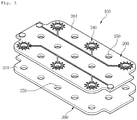
- Fig. 1 is a perspective view of a plasma electrode device according to an embodiment
- Fig. 2 is an enlarged view of a portion "A" of Fig. 1
- Fig. 3 is an exploded perspective view of the plasma electrode device according to the embodiment.
- a plasma electrode device 100 includes first and second substrates 200 and 300 facing each other.
- the second substrate 300 may be disposed below the first substrate 200 and have the same size and shape as the first substrate 200.
- the first and second substrates 200 and 300 may be referred to as an "upper plate” and a “lower plate”, respectively.
- a distance formation part 400 is interposed between the first and second substrates 200 and 300 such that the first and second substrates 200 and 300 are spaced a predetermined distance (d) apart from each other.
- the predetermined distance (d) may have a value of several micrometers ( ⁇ m).
- the first substrate 200 includes a first substrate main body 201 having an approximately rectangular plate shape and at least one first flow hole 250 passing through the first substrate main body 201 to guide an air flow.
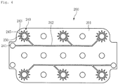
- the first flow hole 250 may be provided in plurality. For example, a total of fifteen first flow holes 250 may be provided as illustrated in Fig. 4 .
- the first substrate 200 includes a first discharge electrode 240 provided with a pattern frame 243 (see Fig. 4 ) disposed to surround at least a portion of the plurality of first flow holes 250.
- the pattern frame 243 may be configured to surround a portion of the plurality of first flow holes 250.
- the pattern frame 243 may be configured to surround six first flow holes 250 of the fifteen first flow holes 250.
- the second substrate 300 includes a second substrate main body 301 having an approximately rectangular plate shape and at least one second flow hole 350 passing through the second substrate main body 301 to guide an air flow.
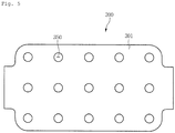
- the second flow hole 350 may be provided in plurality. For example, like the first flow hole 250, a total of fifteen second flow holes 350 may be provided as illustrated in Fig. 5 .
- the plurality of second flow holes 350 may be positioned below the first flow holes 250 to communicate with the first flow holes 250, respectively.
- air passing through the first and second flow holes 250 and 350 may be oxidized or decomposed.
- Fig. 4 is a plan view of the first substrate according to the embodiment
- Fig. 5 is a plan view of the second substrate according to the embodiment
- Fig. 6 is a cross-sectional view taken along line I-I' of Fig. 1 .
- the first substrate 200 includes the first substrate main body 201 in which the plurality of first flow holes 250 are defined and the first discharge electrode 240 provided on one surface of the first substrate main body 201.
- the first substrate main body 201 includes a ground electrode 210, a first insulator 220 surrounding the ground electrode 210, and a photocatalyst 230 provided on at least one surface of the first insulator 220.
- the first discharge electrode 240 includes a discharge electrode 241 to which electric power is applied, the pattern frame 243 surrounding at least one portion of plurality of first flow holes 250, and at least one discharge needle 245 provided on the pattern frame 243.
- the pattern frame 243 may be provided in plurality and has a closed shape surrounding the first flow hole 250.
- the pattern frame may have a shape such as a circular, oval, or polygonal shape.
- the discharge needle 245 protrudes from an outer circumferential surface of the pattern frame 243.
- the first discharge electrode 240 includes a connection line 242 extending from the discharge electrode 241 to the plurality of pattern frames 243.
- the connection line 242 may be branched from the discharge electrode 241 toward the pattern frames 243.
- Metal oxide paste may be printed on the first discharge electrode 240.
- a metallic material of the metal oxide paste may be selected from the group consisting of tungsten, iron, copper, platinum, and silver.
- the metallic material may be silver (Ag).
- silver oxide paste may be printed on the first discharge electrode 240. Since the silver oxide paste has a low resistance of about 10 ⁇ to about 20 ⁇ , the discharge may easily occur due to the low resistance to generate uniform discharge on the entire electrode. In addition, the silver oxide paste may reduce an amount of ozone by discharge.
- the second substrate 300 includes the second substrate main body 301 in which the plurality of second flow holes 350 are defined.
- the second substrate main body 301 includes a second discharge electrode 310 and a second insulator 320 surrounding the second discharge electrode 310.
- the constitutions of the first and second substrate main bodies 201 and 301 will be described below in detail.
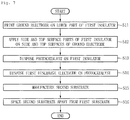
- Fig. 7 is a flowchart illustrating a method of manufacturing a plasma electrode device according to an embodiment.
- the first substrate main body 201 of the first substrate 200 includes the ground electrode 210 acting with the first or second discharge electrode 240 or 310 to generate plasma discharge and the first insulator 220 surrounding the ground electrode 210 to prevent the ground electrode 210 from being exposed to the outside.
- the ground electrode 210 may be provided as a metal plate, for example formed of copper (Cu), and the first insulator 220 may be formed of an epoxy resin. The first insulator 220 may be disposed to surround both side surfaces and top and bottom surfaces of the ground electrode 210.
- Cu copper
- the first insulator 220 may be disposed to surround both side surfaces and top and bottom surfaces of the ground electrode 210.
- the first insulator 220 includes a bottom surface part 221 on which the ground electrode 210 is seated, side surface parts 222 extending upward from each of both sides of the bottom surface part 221, and an top surface part 223 covering an upper side of the side surface part 222.
- An outer surface of the ground electrode 210 is completely surrounded by the bottom, side, and top surface parts 221, 222, and 223 of the first insulator 220.
- ground electrode 210 and the first insulator 220 A method of manufacturing the ground electrode 210 and the first insulator 220 will be described below in brief.
- the ground electrode 210 is masked on the bottom surface part 221 of the first insulator 220.
- the bottom surface part 221 is formed of an epoxy resin and may be understood as a base on which the ground electrode 210 is disposed (S11).
- ground electrode 210 When the ground electrode 210 is marked, a lower surface of the ground electrode 210 is covered by the first insulator 220, and side and top surfaces of the ground electrode 210 are exposed to the outside.
- the side and top surface parts 222 and 223 of the first insulator 220 are coated on the side and top surfaces of the ground electrode 210 exposed to the outside.
- the coated side and top surface parts 222 and 223 may be formed of the same epoxy resin as the bottom surface part 221 (S12).
- the photocatalyst 230 which reacts with or is activated by visible light, is disposed on the first insulator 220 (S13). In other words, the photocatalyst 230 is interposed between the first insulator 220 and the first discharge electrode 240.
- the photocatalyst 230 may easily decompose various harmful substances, perform antibacterial and germicidal functions, and reduce ozone.
- the visible light is understood as light emitted from an external light source disposed outside the plasma electrode device 100.
- the visible light may include natural light or light emitted from a lighting source existing in a predetermined space.
- the photocatalyst 230 includes a variety of compositions.
- the compositions may include silver phosphate (Ag 3 PO 4 ), titanium dioxide (TiO 2 ) and inorganic binder.
- the photocatalyst 230 may include about 20 parts to about 50 parts by weight of silver phosphate (Ag 3 PO 4 ), about 5 parts to about 40 parts by weight of titanium dioxide (TiO 2 ), and about 10 parts to about 40 parts by weight of inorganic binder.
- the titanium dioxide (TiO 2 ) may exhibit high activity under ultraviolet radiation and be stable chemically without being eroded by acidic, alkaline, and an organic solvent.
- the silver phosphate may undergo catalytic activity reaction by light energy of visible light in a wavelength band of about 385 nm or more, an average wavelength of which is about 500 nm.
- the titanium dioxide is mixed with the silver phosphate so that the photocatalyst is effectively activated by the visible light.
- the silver phosphate may have a synergy effect of decomposing organic matters (microorganisms and stinking components) through simultaneous activation with titanium dioxide in a low-energy region (in the visible-light wavelength region), in addition to antibacterial performance itself against bacteria, fungi, and the like.
- the inorganic binder includes a poly-silicate compound.
- the poly-silicate compound may consist of colloidal silica (SiO 2 ) and metal alkoxide.
- the inorganic binder may additionally include other components.
- the other components may be selected by those skilled in the art in consideration of characteristics of a finally produced coating composition.
- the other components may include a stabilizer, an acid catalyst, a curing agent, a metallic additive, and the like.
- the stabilizer may be selected from the group consisting of acetylacetone, ethyl acetoacetate, iron acetylacetone, alkanolamine, and combinations thereof.
- the inorganic binder may include about 0.1 parts to about 0.5 parts by weight of the stabilizer.
- the acid catalyst may be selected from the group consisting of a phosphoric acid metal catalyst, a hydrochloric acid metal catalyst, a nitric acid metal catalyst, a phosphoric-hydrochloric acid composite metal catalyst, and a combination thereof.
- the inorganic binder may include about 0.01 parts to about 0.5 parts by weight of the acid catalyst.
- the curing agent may be selected from the group consisting of aliphatic polyamine, acrylonitrile modified amine, polyamide, amidoamine, dicyandiamide, amide resin, isocyanate, melamine, and a combination thereof.
- the inorganic binder may include about 0.05 parts to about 1 part by weight of the curing agent.
- the metallic additive may include an aluminum compound.
- the aluminum compound may be prepared by mixing aluminum isopropoxide with aluminum chloride.
- the inorganic binder may include about 0.05 parts to about 0.5 parts by weight of the metallic additive.
- the photocatalyst 230 may be prepared in a liquid state in which the plurality of compositions are mixed with a predetermined solvent and coupled to the top surface part 223 of the first insulator 220.
- the photocatalyst 230 may be coupled to the top surface part 223 by the coating.
- the coating may be performed through, for example, dip coating, spray coating, screen printing, or the like.
- a drying temperature may vary according to characteristics of a coating base material, for example, the drying process may be performed at a temperature of about 148°C to about 152°C for about 9 minutes to about 11 minutes.
- the photocatalyst 230 may be produced in a liquid state and coated on the first insulator 220. Therefore, the photocatalyst 230 may be easily coupled to the surface of the insulator 220 (an adhesive force being secured).
- the photocatalyst 230 having the above-described components When the photocatalyst 230 having the above-described components is provided on the top surface part 223, water (H 2 O) or oxygen (O 2 ) may be converted into reactive oxygen species (ROS) by the catalysis of the photocatalyst 230.
- the reactive oxygen species include hydroxyl radical (OH - ), hydrogen peroxide (H 2 O 2 ), and the like.
- the reactive oxygen species may perform strong germicidal (oxidation) and deodorization actions.
- the reactive oxygen species may decompose gas pollutants, such as toluene and ammonia, as well as biological pollutants, such as bacteria or fungi composed of organic matter, into water harmless to the humans and carbon dioxide. Therefore, the photocatalyst 230 may prevent creation of pollutants resulting from air or moisture, that is, accumulation of dust or propagation of microorganisms.
- the first discharge electrode 240 may be disposed on the photocatalyst 230. As described above, the first discharge electrode 240 may be printed with a metal oxide paste on the top surface of the photocatalyst 230 (S14). The first substrate 200 may be completely manufactured through the operations S11 to S14.
- the first discharge electrode 240 may be understood as an electrode for generating ions.
- the second substrate 300 may be manufactured.
- the second substrate 300 is disposed to be spaced downward from the first substrate 200.
- the second substrate main body 301 of the second substrate 300 includes the second discharge electrode 310 acting with the ground electrode 210 to perform plasma discharge and the second insulator 320 surrounding the second discharge electrode 310 to prevent the second discharge electrode 310 from being exposed to the outside.
- the second discharge electrode 310 may be formed of metal, for example, copper (Cu), and the second insulator 320 may be formed of an epoxy resin.
- the second insulator 320 includes a bottom surface part 321 on which the second discharge electrode 310 is disposed, a side surface part 322 extending upward from each of both sides of the bottom surface part 321, and a top surface part 323 covering an upper side of the side surface part.
- An outer surface of the second discharge electrode 310 is completely surrounded by the lower, side, and top surface parts of the second insulator 320.
- the second discharge electrode 310 is masked on the bottom surface part 321 of the second insulator 320.
- the bottom surface part 321 is formed of an epoxy resin and may be understood as a base on which the second discharge electrode 310 is disposed.
- the side and top surface parts 322 and 323 of the second insulator 320 are coated on the side and top surfaces of the second discharge electrode 310 exposed to the outside.
- the coated side and top surface parts 322 and 323 may be formed of the same epoxy resin as the bottom surface part 321.
- the photocatalyst 230 which reacts with or is activated by visible light, is disposed on the second insulator 320.
- the second substrate 300 including the second discharge electrode 310 and the second insulator 320 which are manufactured in the above-described method may be disposed to be spaced a distance corresponding to the distance formation part 400 downward from the first substrate 200 (S15 and S16).
- the lower, side, and top surface parts 221, 222, and 223 of the first insulator 220 may be referred to as a first base, a first side surface part, and a first top surface part, respectively.
- the lower, side, and top surface parts 321, 322, and 323 may be referred to as a second base, a second side surface part, and a second top surface part, respectively.
- the second discharge electrode 310 is disposed to be spaced a distance corresponding to the distance formation part 400 from the ground electrode 210 and thus understood as a "surface discharge electrode" for generating radical ions.
- the plasma electrode device can generate a large amount of ions by the plasma discharge of the ground electrode and the first discharge electrode, resulting in easily removing pollutants or smells resulting from a predetermined place.
- the plasma electrode device can generate a large amount of radicals by the plasma discharge (surface discharge) of the ground electrode and the second discharge electrode to easily remove smells in the air.
- the photocatalyst in the plasma electrode device can easily decompose the harmful substances, perform the antibacterial and germicidal functions, and reduce the ozone.
- the plasma electrode device includes the first substrate provided with the first discharge electrode and the ground electrode and the second substrate provided with the second discharge electrode to generate a large amount of ions through the interaction between the first discharge electrode and the ground electrode and a large amount of radicals through the interaction between the second discharge electrode and the ground electrode.
- the pollutants or smells resulting from a predetermined place can be easily removed using the large amount of ions, and smells in the air can be easily removed using the large amount of radicals.
- the insulator formed of an epoxy resin is disposed to surround the electrode provided as the metal plate, thereby easily generating the plasma discharge.
- the plasma electrode device includes the photocatalyst reacting with the visible light to easily decompose the various harmful substances, perform the antibacterial and germicidal functions, and reduce the ozone.
Landscapes
- Chemical & Material Sciences (AREA)
- Engineering & Computer Science (AREA)
- Health & Medical Sciences (AREA)
- Physics & Mathematics (AREA)
- Analytical Chemistry (AREA)
- Chemical Kinetics & Catalysis (AREA)
- Plasma & Fusion (AREA)
- General Health & Medical Sciences (AREA)
- Public Health (AREA)
- Veterinary Medicine (AREA)
- Animal Behavior & Ethology (AREA)
- Epidemiology (AREA)
- Life Sciences & Earth Sciences (AREA)
- General Chemical & Material Sciences (AREA)
- Oil, Petroleum & Natural Gas (AREA)
- Organic Chemistry (AREA)
- Toxicology (AREA)
- Electromagnetism (AREA)
- Environmental & Geological Engineering (AREA)
- Biomedical Technology (AREA)
- Spectroscopy & Molecular Physics (AREA)
- Combustion & Propulsion (AREA)
- Mechanical Engineering (AREA)
- General Engineering & Computer Science (AREA)
- Disinfection, Sterilisation Or Deodorisation Of Air (AREA)
- Physical Or Chemical Processes And Apparatus (AREA)
Description
- The present disclosure relates to a plasma electrode device.
- Recently, constructed buildings receive minimum external air and are sealed off from the outside for energy saving, and thus air pollution therein becomes more serious. Accordingly, mandatory regulations for indoor pollutants are being increasingly reinforced.
- Meanwhile, during operations of home appliances installed at home or offices, indoor pollutants may be stuck to or discharged from the home appliances. The indoor pollutants may cause unpleasant smells and have a negative influence on user's health. For example, in the case of home appliances, such as air conditioners, dehumidifiers, air cleaners, refrigerators, and washing machines, which use air containing moisture or water, contamination due to dust or microorganisms may occur inside or outside the home appliances.
- More specifically, the indoor pollutants may be classified into (1) particulate pollutants such as fine dust and asbestos, (2) gaseous pollutants such as carbon dioxide, formaldehyde, and volatile organic compounds (VOC), and (3) biological pollutants such as virus, fungi, and bacteria.
- Surface discharge plasma chemical processing may be used to remove such indoor pollutants. In general, in the surface discharge plasma chemical processing, high intensity plasma is generated on a device surface by high frequency discharge using ceramics to generate a large amount of OH radicals, and then the pollutants are removed by the OH radicals and ozone in the plasma.
- One example of the following technique (hereinafter, referred to as "the related art") is disclosed in Korean Patent No.
10-0657476 (issued on December 7, 2006 - The air cleaning device according to the related art includes a discharge electrode provided on a top surface of two sheet of insulating dielectrics that are attached to each other, a ground electrode interposed between the two sheet of insulating dielectrics, and a coating layer sealing the discharge electrode to prevent the discharge electrode from being directly exposed to the air. Here, each of the insulating dielectrics may be coated with an insulating material. For example, the insulating material includes ceramics.
- When the insulating dielectric is coated with the insulating material or includes the coating layer, the surface of the electrode has to be uniformly coated to generate uniform discharge. However, in the case of the plasma electrode device according to the related art, it is very difficult to form the coating having a uniform thickness, and uneven patterns beyond an allowable range are formed on the surface in the coating process.
- In addition, the plasma electrode device according to the related art may generate an insufficient amount of ions, and thus it may be difficult to remove effectively pollutants. Further, a large amount of ozone that is harmful to humans may be generated during the plasma discharge.
-
JP 2010 033867 A US 2005/118079 A1 relates to a method and an apparatus for gas treatment, which can be performed using non-equilibrium plasma caused by use of discharge electrodes with a relatively low cost. - Embodiments provide a plasma electrode device that is capable of removing pollutants.
- In one embodiment, a plasma electrode device includes: a first substrate including a first substrate main body having a first flow hole through which air flows and a first discharge electrode disposed on one surface of the first substrate main body; and a second substrate disposed on one side of the first substrate, the second substrate including a second flow hole through which air flows and a second discharge electrode acting with the first substrate, wherein the first substrate main body includes: a ground electrode acting with the first or second discharge electrode to perform plasma discharge; and a first insulator coupled to the ground electrode.
- The first insulator may be disposed to surround the ground electrode.
- The first insulator may include: a first base on which the ground electrode is seated; a first side surface part extending from each of both sides of the first base to surround a side surface of the ground electrode; and a first top surface part extending from the first side surface part to cover a top surface of the ground electrode.
- The second substrate may include a second insulator surrounding the second discharge electrode.
- The second insulator may include: a second base on which the second discharge electrode is seated; a second side surface part extending from each of both sides of the second base to surround a side surface of the second discharge electrode; and a second top surface part extending from the second side surface part to cover a top surface of the second discharge electrode.
- A distance formation part may be disposed between the first and second substrates to allow the second substrate to be spaced a predetermined distance (d) from the first substrate.
- The predetermined distance (d) may have a value of several micrometers (µm).
- The first or second insulator may be formed of an epoxy resin.
- A photocatalyst activated by visible light to decompose a pollutant or reduce ozone may be disposed between the first insulator and the first discharge electrode.
- The photocatalyst may include silver phosphate (Ag3PO4), titanium dioxide (TiO2), and inorganic binder.
- The first flow hole may be provided in plurality, and the second flow hole may have the same number as the plurality of flow holes to communicate with the first flow holes.
- The first discharge electrode may include: a discharge electrode to which electric power is applied; a pattern frame surrounding the first flow hole and having a preset shape; and at least one discharge needle provided on the pattern frame.
- The first flow hole may be provided in plurality, and the pattern frame may be disposed to surround a portion of the plurality of first flow holes.
- In another embodiment, a method for manufacturing a plasma electrode device include: manufacturing a first substrate, wherein the manufacturing of the first substrate includes: disposing a ground electrode on a bottom surface part of a first insulator; covering the ground electrode by using side and top surface parts of the first insulator; disposing a photocatalyst on the first insulator; and disposing a first discharge electrode on the photocatalyst.
- The method may further include: manufacturing a second substrate; and spacing the second substrate apart from the first substrate by a distance corresponding to a distance formation part, wherein the manufacturing of the second substrate may include: disposing a second discharge electrode on a bottom surface part of a second insulator; and covering side and top surfaces of the second discharge electrode, which are exposed to the outside, with side and top surface parts of the second insulator.
- In further another embodiment, a plasma electrode device includes: a first substrate provided with a first substrate main body including a ground electrode and a photocatalyst and a first discharge electrode disposed on one surface of the first substrate main body; a first insulator provided on the first substrate main body to surround the ground electrode; a second substrate disposed on one side of the first substrate, the second substrate including a second substrate main body provided with a second discharge electrode acting with the ground electrode; a second insulator provided on the second substrate main body to surround the second discharge electrode; and a distance formation part spacing the first substrate apart from the second substrate.
- The first substrate may further include a first substrate main body having a plurality of first flow holes through which air flows, and the first discharge electrode may be disposed on one surface of the first substrate main body.
- The first discharge electrode may include: a discharge electrode to which electric power is applied; a pattern frame disposed outside the first flow holes, and the pattern frame having a closed shape; and at least one discharge needle protruding from an outer circumferential surface of the pattern frame.
- The pattern frame may have one of circular, oval, and polygonal shapes.
- A plurality of second flow holes may be defined in the second substrate main body to correspond to the plurality of first flow holes.
- The details of one or more embodiments are set forth in the accompanying drawings and the description below. Other features will be apparent from the description and drawings, and from the claims.
-
-
Fig. 1 is a perspective view of a plasma electrode device according to an embodiment. -
Fig. 2 is an enlarged view of a portion "A" ofFig. 1 . -
Fig. 3 is an exploded perspective view of the plasma electrode device according to the embodiment. -
Fig. 4 is a plan view of a first substrate according to an embodiment. -
Fig. 5 is a plan view of a second substrate according to an embodiment. -
Fig. 6 is a cross-sectional view taken along line I-I' ofFig. 1 . -
Fig. 7 is a flowchart illustrating a method of manufacturing a plasma electrode device according to an embodiment. - Hereinafter, exemplary embodiments will be described with reference to the accompanying drawings. However, the spirit of the present disclosure is not limited to the disclosed embodiments, and those skilled in the art that understands the spirit of the present disclosure will be able to readily propose other embodiments without departing from the scope of the present disclosure.
-
Fig. 1 is a perspective view of a plasma electrode device according to an embodiment,Fig. 2 is an enlarged view of a portion "A" ofFig. 1 , andFig. 3 is an exploded perspective view of the plasma electrode device according to the embodiment. - Referring to
Figs. 1 to 3 , aplasma electrode device 100 according to an embodiment includes first andsecond substrates second substrate 300 may be disposed below thefirst substrate 200 and have the same size and shape as thefirst substrate 200. The first andsecond substrates - In detail, a
distance formation part 400 is interposed between the first andsecond substrates second substrates - The
first substrate 200 includes a first substratemain body 201 having an approximately rectangular plate shape and at least onefirst flow hole 250 passing through the first substratemain body 201 to guide an air flow. Thefirst flow hole 250 may be provided in plurality. For example, a total of fifteenfirst flow holes 250 may be provided as illustrated inFig. 4 . - The
first substrate 200 includes afirst discharge electrode 240 provided with a pattern frame 243 (seeFig. 4 ) disposed to surround at least a portion of the plurality offirst flow holes 250. Thepattern frame 243 may be configured to surround a portion of the plurality of first flow holes 250. For example, thepattern frame 243 may be configured to surround six first flow holes 250 of the fifteen first flow holes 250. - The
second substrate 300 includes a second substratemain body 301 having an approximately rectangular plate shape and at least onesecond flow hole 350 passing through the second substratemain body 301 to guide an air flow. Thesecond flow hole 350 may be provided in plurality. For example, like thefirst flow hole 250, a total of fifteen second flow holes 350 may be provided as illustrated inFig. 5 . The plurality of second flow holes 350 may be positioned below the first flow holes 250 to communicate with the first flow holes 250, respectively. - When the
plasma electrode device 100 operates to generate plasma discharge, air passing through the first and second flow holes 250 and 350 may be oxidized or decomposed. -
Fig. 4 is a plan view of the first substrate according to the embodiment,Fig. 5 is a plan view of the second substrate according to the embodiment, andFig. 6 is a cross-sectional view taken along line I-I' ofFig. 1 . - Referring to
Figs. 4 and6 , thefirst substrate 200 according to the embodiment includes the first substratemain body 201 in which the plurality of first flow holes 250 are defined and thefirst discharge electrode 240 provided on one surface of the first substratemain body 201. - The first substrate
main body 201 includes aground electrode 210, afirst insulator 220 surrounding theground electrode 210, and aphotocatalyst 230 provided on at least one surface of thefirst insulator 220. - The
first discharge electrode 240 includes adischarge electrode 241 to which electric power is applied, thepattern frame 243 surrounding at least one portion of plurality of first flow holes 250, and at least onedischarge needle 245 provided on thepattern frame 243. - The
pattern frame 243 may be provided in plurality and has a closed shape surrounding thefirst flow hole 250. For example, the pattern frame may have a shape such as a circular, oval, or polygonal shape. Thedischarge needle 245 protrudes from an outer circumferential surface of thepattern frame 243. - The
first discharge electrode 240 includes aconnection line 242 extending from thedischarge electrode 241 to the plurality of pattern frames 243. Theconnection line 242 may be branched from thedischarge electrode 241 toward the pattern frames 243. - Metal oxide paste may be printed on the
first discharge electrode 240. A metallic material of the metal oxide paste may be selected from the group consisting of tungsten, iron, copper, platinum, and silver. For example, the metallic material may be silver (Ag). - For example, silver oxide paste may be printed on the
first discharge electrode 240. Since the silver oxide paste has a low resistance of about 10 Ω to about 20 Ω, the discharge may easily occur due to the low resistance to generate uniform discharge on the entire electrode. In addition, the silver oxide paste may reduce an amount of ozone by discharge. - Referring to
Fig.5 , thesecond substrate 300 according to the embodiment includes the second substratemain body 301 in which the plurality of second flow holes 350 are defined. The second substratemain body 301 includes asecond discharge electrode 310 and asecond insulator 320 surrounding thesecond discharge electrode 310. The constitutions of the first and second substratemain bodies -
Fig. 7 is a flowchart illustrating a method of manufacturing a plasma electrode device according to an embodiment. - Referring to
Figs. 6 and7 , the first substratemain body 201 of thefirst substrate 200 according to the embodiment includes theground electrode 210 acting with the first orsecond discharge electrode first insulator 220 surrounding theground electrode 210 to prevent theground electrode 210 from being exposed to the outside. - The
ground electrode 210 may be provided as a metal plate, for example formed of copper (Cu), and thefirst insulator 220 may be formed of an epoxy resin. Thefirst insulator 220 may be disposed to surround both side surfaces and top and bottom surfaces of theground electrode 210. - In detail, the
first insulator 220 includes abottom surface part 221 on which theground electrode 210 is seated,side surface parts 222 extending upward from each of both sides of thebottom surface part 221, and antop surface part 223 covering an upper side of theside surface part 222. An outer surface of theground electrode 210 is completely surrounded by the bottom, side, andtop surface parts first insulator 220. - A method of manufacturing the
ground electrode 210 and thefirst insulator 220 will be described below in brief. - The
ground electrode 210 is masked on thebottom surface part 221 of thefirst insulator 220. Here, thebottom surface part 221 is formed of an epoxy resin and may be understood as a base on which theground electrode 210 is disposed (S11). - When the
ground electrode 210 is marked, a lower surface of theground electrode 210 is covered by thefirst insulator 220, and side and top surfaces of theground electrode 210 are exposed to the outside. - The side and
top surface parts first insulator 220 are coated on the side and top surfaces of theground electrode 210 exposed to the outside. In this case, the coated side andtop surface parts - The
photocatalyst 230, which reacts with or is activated by visible light, is disposed on the first insulator 220 (S13). In other words, thephotocatalyst 230 is interposed between thefirst insulator 220 and thefirst discharge electrode 240. Thephotocatalyst 230 may easily decompose various harmful substances, perform antibacterial and germicidal functions, and reduce ozone. - The visible light is understood as light emitted from an external light source disposed outside the
plasma electrode device 100. For example, the visible light may include natural light or light emitted from a lighting source existing in a predetermined space. - The
photocatalyst 230 includes a variety of compositions. In detail, the compositions may include silver phosphate (Ag3PO4), titanium dioxide (TiO2) and inorganic binder. For example, thephotocatalyst 230 may include about 20 parts to about 50 parts by weight of silver phosphate (Ag3PO4), about 5 parts to about 40 parts by weight of titanium dioxide (TiO2), and about 10 parts to about 40 parts by weight of inorganic binder. - The titanium dioxide (TiO2) may exhibit high activity under ultraviolet radiation and be stable chemically without being eroded by acidic, alkaline, and an organic solvent.
- The silver phosphate (Ag3PO4) may undergo catalytic activity reaction by light energy of visible light in a wavelength band of about 385 nm or more, an average wavelength of which is about 500 nm. The titanium dioxide is mixed with the silver phosphate so that the photocatalyst is effectively activated by the visible light. In addition, the silver phosphate may have a synergy effect of decomposing organic matters (microorganisms and stinking components) through simultaneous activation with titanium dioxide in a low-energy region (in the visible-light wavelength region), in addition to antibacterial performance itself against bacteria, fungi, and the like.
- The inorganic binder includes a poly-silicate compound. The poly-silicate compound may consist of colloidal silica (SiO2) and metal alkoxide. In addition, the inorganic binder may additionally include other components. The other components may be selected by those skilled in the art in consideration of characteristics of a finally produced coating composition. For example, the other components may include a stabilizer, an acid catalyst, a curing agent, a metallic additive, and the like.
- The stabilizer may be selected from the group consisting of acetylacetone, ethyl acetoacetate, iron acetylacetone, alkanolamine, and combinations thereof. The inorganic binder may include about 0.1 parts to about 0.5 parts by weight of the stabilizer.
- The acid catalyst may be selected from the group consisting of a phosphoric acid metal catalyst, a hydrochloric acid metal catalyst, a nitric acid metal catalyst, a phosphoric-hydrochloric acid composite metal catalyst, and a combination thereof. The inorganic binder may include about 0.01 parts to about 0.5 parts by weight of the acid catalyst.
- The curing agent may be selected from the group consisting of aliphatic polyamine, acrylonitrile modified amine, polyamide, amidoamine, dicyandiamide, amide resin, isocyanate, melamine, and a combination thereof. The inorganic binder may include about 0.05 parts to about 1 part by weight of the curing agent.
- The metallic additive may include an aluminum compound. The aluminum compound may be prepared by mixing aluminum isopropoxide with aluminum chloride. The inorganic binder may include about 0.05 parts to about 0.5 parts by weight of the metallic additive.
- The
photocatalyst 230 may be prepared in a liquid state in which the plurality of compositions are mixed with a predetermined solvent and coupled to thetop surface part 223 of thefirst insulator 220. - For example, the
photocatalyst 230 may be coupled to thetop surface part 223 by the coating. The coating may be performed through, for example, dip coating, spray coating, screen printing, or the like. In the case of the dip coating, a drying temperature may vary according to characteristics of a coating base material, for example, the drying process may be performed at a temperature of about 148°C to about 152°C for about 9 minutes to about 11 minutes. As described above, thephotocatalyst 230 may be produced in a liquid state and coated on thefirst insulator 220. Therefore, thephotocatalyst 230 may be easily coupled to the surface of the insulator 220 (an adhesive force being secured). - When the
photocatalyst 230 having the above-described components is provided on thetop surface part 223, water (H2O) or oxygen (O2) may be converted into reactive oxygen species (ROS) by the catalysis of thephotocatalyst 230. The reactive oxygen species include hydroxyl radical (OH-), hydrogen peroxide (H2O2), and the like. - The reactive oxygen species may perform strong germicidal (oxidation) and deodorization actions. In detail, the reactive oxygen species may decompose gas pollutants, such as toluene and ammonia, as well as biological pollutants, such as bacteria or fungi composed of organic matter, into water harmless to the humans and carbon dioxide. Therefore, the
photocatalyst 230 may prevent creation of pollutants resulting from air or moisture, that is, accumulation of dust or propagation of microorganisms. - The
first discharge electrode 240 may be disposed on thephotocatalyst 230. As described above, thefirst discharge electrode 240 may be printed with a metal oxide paste on the top surface of the photocatalyst 230 (S14). Thefirst substrate 200 may be completely manufactured through the operations S11 to S14. - An operation of the above-described
first substrate 200 will be described below in brief. - When a high voltage greater than a threshold voltage is applied to the
first discharge electrode 240 provided with thepattern frame 243, a discharge phenomenon occurs around theground electrode 210 and thefirst discharge electrode 240 due to high electric fields. - Free electrons passing around the
ground electrode 210 and thefirst discharge electrode 240 are accelerated by the electric fields and collide with neutral molecules (oxygen and nitrogen) in the air to ionize the molecules, thereby generating a large amount of ions. In this case, the air may be air passing through the first flow holes 250. Thefirst discharge electrode 240 may be understood as an electrode for generating ions. - After the manufacturing of the
first substrate 200, thesecond substrate 300 may be manufactured. Thesecond substrate 300 is disposed to be spaced downward from thefirst substrate 200. - In detail, the second substrate
main body 301 of thesecond substrate 300 includes thesecond discharge electrode 310 acting with theground electrode 210 to perform plasma discharge and thesecond insulator 320 surrounding thesecond discharge electrode 310 to prevent thesecond discharge electrode 310 from being exposed to the outside. - The
second discharge electrode 310 may be formed of metal, for example, copper (Cu), and thesecond insulator 320 may be formed of an epoxy resin. - The
second insulator 320 includes abottom surface part 321 on which thesecond discharge electrode 310 is disposed, aside surface part 322 extending upward from each of both sides of thebottom surface part 321, and atop surface part 323 covering an upper side of the side surface part. An outer surface of thesecond discharge electrode 310 is completely surrounded by the lower, side, and top surface parts of thesecond insulator 320. - A method of manufacturing the
second discharge electrode 310 and thesecond insulator 320 will be described below in brief. - The
second discharge electrode 310 is masked on thebottom surface part 321 of thesecond insulator 320. Here, thebottom surface part 321 is formed of an epoxy resin and may be understood as a base on which thesecond discharge electrode 310 is disposed. - The side and
top surface parts second insulator 320 are coated on the side and top surfaces of thesecond discharge electrode 310 exposed to the outside. In this case, the coated side andtop surface parts bottom surface part 321. - The
photocatalyst 230, which reacts with or is activated by visible light, is disposed on thesecond insulator 320. - The
second substrate 300 including thesecond discharge electrode 310 and thesecond insulator 320 which are manufactured in the above-described method may be disposed to be spaced a distance corresponding to thedistance formation part 400 downward from the first substrate 200 (S15 and S16). - The lower, side, and
top surface parts first insulator 220 may be referred to as a first base, a first side surface part, and a first top surface part, respectively. Also, the lower, side, andtop surface parts - An operation of the
second substrate 300 including the above-described constitutions andground electrode 210 will be described below in brief. - When a high voltage greater than a threshold voltage is applied to the
second discharge electrode 310, dielectric breakdown occurs between theground electrode 210 and thesecond discharge electrode 310, and a discharge phenomenon takes place due to high electric fields, thereby forming a high intensity plasma region. - Free electrons passing around the plasma region are accelerated by the electric field to react with air, and as a result, a large amount of OH radical is generated. In this case, the air may be air passing through the
second flow hole 350. Thesecond discharge electrode 310 is disposed to be spaced a distance corresponding to thedistance formation part 400 from theground electrode 210 and thus understood as a "surface discharge electrode" for generating radical ions. - In summary, the plasma electrode device according to the embodiment can generate a large amount of ions by the plasma discharge of the ground electrode and the first discharge electrode, resulting in easily removing pollutants or smells resulting from a predetermined place.
- In addition, the plasma electrode device can generate a large amount of radicals by the plasma discharge (surface discharge) of the ground electrode and the second discharge electrode to easily remove smells in the air.
- Further, the photocatalyst in the plasma electrode device can easily decompose the harmful substances, perform the antibacterial and germicidal functions, and reduce the ozone.
- According to the embodiments, the plasma electrode device includes the first substrate provided with the first discharge electrode and the ground electrode and the second substrate provided with the second discharge electrode to generate a large amount of ions through the interaction between the first discharge electrode and the ground electrode and a large amount of radicals through the interaction between the second discharge electrode and the ground electrode.
- In addition, the pollutants or smells resulting from a predetermined place can be easily removed using the large amount of ions, and smells in the air can be easily removed using the large amount of radicals.
- Further, the insulator formed of an epoxy resin is disposed to surround the electrode provided as the metal plate, thereby easily generating the plasma discharge.
- Furthermore, the plasma electrode device includes the photocatalyst reacting with the visible light to easily decompose the various harmful substances, perform the antibacterial and germicidal functions, and reduce the ozone.
- Although embodiments have been described with reference to a number of illustrative embodiments thereof, it should be understood that numerous other modifications and embodiments can be devised by those skilled in the art that will fall within the scope of the principles of this disclosure. More particularly, various variations and modifications are possible in the component parts and/or arrangements of the subject combination arrangement within the scope of the disclosure, the drawings and the appended claims. The invention is defined by the appended claims. In addition to variations and modifications in the component parts and/or arrangements, alternative uses will also be apparent to those skilled in the art.
Claims (13)
- A plasma electrode device (100) comprising:a first substrate (200) comprising a first substrate main body (201) having a first flow hole (250) through which air is flowable and a first discharge electrode (240) disposed on a surface of the first substrate main body (201); anda second substrate (300) disposed on one side of the first substrate (200), the second substrate (300) comprising a second flow hole (350) through which air is flowable and a second discharge electrode (310) acting with the first substrate (200),characterized in that the first substrate main body (201) comprises:a ground electrode (210) acting with the first or second discharge electrode (240, 310) for generating plasma discharge; anda first insulator (220) coupled to the ground electrode (210) to surround the ground electrode (210), wherein the first insulator (220) comprises:a first base on which the ground electrode (210) is seated;a first side surface part extending from each of both sides of the first base to surround a side surface of the ground electrode (210); anda first top surface part extending from the first side surface part to cover a top surface of the ground electrode (210).
- The plasma electrode device (100) according to claim 1, wherein the second substrate (300) comprises a second insulator (320) surrounding the second discharge electrode (310).
- The plasma electrode device (100) according to claim 2, wherein the second insulator (320) comprises:a second base on which the second discharge electrode (310) is seated;a second side surface part extending from each of both sides of the second base to surround a side surface of the second discharge electrode (310); anda second top surface part extending from the second side surface part to cover a top surface of the second discharge electrode (310).
- The plasma electrode device (100) according to any one of claims 1 to 3, further comprising a distance formation part disposed between the first and second substrates (200, 300) to allow the second substrate (300) to be spaced a predetermined distance (d) from the first substrate (200).
- The plasma electrode device (100) according to claim 4, wherein the predetermined distance (d) has a value of several micrometers (µm).
- The plasma electrode device (100) according to any one of claims 2 to 5, wherein the first or second insulator (220, 320) is formed of an epoxy resin.
- The plasma electrode device (100) according to any one of claims 1 to 6, further comprising a photocatalyst (230) disposed between the first insulator (220) and the first discharge electrode (240) and activated by visible light for decomposing a pollutant or reduce ozone.
- The plasma electrode device (100) according to claim 7, wherein the photocatalyst (230) comprises silver phosphate (Ag3PO4), titanium dioxide (TiO2), and inorganic binder.
- The plasma electrode device (100) according to any one of claims 1 to 8, wherein the first flow hole (250) is provided in plurality, and
the second flow hole (350) has the same number as the plurality of the first flow holes (250) to communicate with the first flow holes (250). - The plasma electrode device (100) according to any one of claims 1 to 9, wherein the first discharge electrode (240) comprises:a discharge electrode (241) to which electric power is applied;a pattern frame (243) surrounding the first flow hole (250) and having a preset shape; andat least one discharge needle (245) provided on the pattern frame (243).
- The plasma electrode device (100) according to claim 10, wherein the first flow hole (250) is provided in plurality, and
the pattern frame (243) is disposed to surround a portion of the plurality of first flow holes (250). - A method for manufacturing a plasma electrode device (100), comprising:manufacturing a first substrate (200),wherein the manufacturing of the first substrate (200) comprises:disposing (S11) a ground electrode (210) on a bottom surface part (221) of a first insulator (220);covering (S12) the ground electrode (210) by using side and top surface parts of the first insulator (220);disposing (S13) a photocatalyst (230) on the first insulator (220); anddisposing (S14) a first discharge electrode (240) on the photocatalyst (230).
- The method according to claim 12, further comprising:manufacturing (S15) a second substrate (300); andspacing (S16) the second substrate (300) apart from the first substrate (200) by a distance corresponding to a distance formation part (400),wherein the manufacturing of the second substrate (300) comprises:disposing a second discharge electrode (310) on a bottom surface part of a second insulator (320); andcovering side and top surfaces of the second discharge electrode (310), which are exposed to the outside, with side and top surface parts of the second insulator (320).
Applications Claiming Priority (1)
| Application Number | Priority Date | Filing Date | Title |
|---|---|---|---|
| KR1020140034441A KR102186432B1 (en) | 2014-03-25 | 2014-03-25 | A plasma electrode device |
Publications (2)
| Publication Number | Publication Date |
|---|---|
| EP2923752A1 EP2923752A1 (en) | 2015-09-30 |
| EP2923752B1 true EP2923752B1 (en) | 2020-09-30 |
Family
ID=52394173
Family Applications (1)
| Application Number | Title | Priority Date | Filing Date |
|---|---|---|---|
| EP15152460.0A Active EP2923752B1 (en) | 2014-03-25 | 2015-01-26 | Plasma electrode device and method for manufacturing the same |
Country Status (4)
| Country | Link |
|---|---|
| US (1) | US9646806B2 (en) |
| EP (1) | EP2923752B1 (en) |
| KR (1) | KR102186432B1 (en) |
| CN (1) | CN104955258B (en) |
Families Citing this family (24)
| Publication number | Priority date | Publication date | Assignee | Title |
|---|---|---|---|---|
| KR102186432B1 (en) | 2014-03-25 | 2020-12-03 | 엘지전자 주식회사 | A plasma electrode device |
| KR102259353B1 (en) | 2014-07-16 | 2021-06-02 | 엘지전자 주식회사 | Sterilized apparatus |
| KR101666621B1 (en) * | 2015-10-22 | 2016-10-17 | 주식회사 에코셋 | Double dielectric barrier discharge plasma reactor, purification apparatus including the same, and purification method using the same |
| CN105232144B (en) * | 2015-11-18 | 2017-07-21 | 南京亿高微波系统工程有限公司 | A kind of plasma kinetic system and its control method for ent surgery |
| KR20170068232A (en) * | 2015-12-09 | 2017-06-19 | 엘지전자 주식회사 | Plasma electrode device, method of manufacturing the same and air conditioner |
| KR101632158B1 (en) * | 2015-12-28 | 2016-06-21 | 광운대학교 산학협력단 | Sterilizer for vehicle or room with plasma |
| US10980911B2 (en) | 2016-01-21 | 2021-04-20 | Global Plasma Solutions, Inc. | Flexible ion generator device |
| US11283245B2 (en) | 2016-08-08 | 2022-03-22 | Global Plasma Solutions, Inc. | Modular ion generator device |
| KR102053339B1 (en) * | 2016-12-22 | 2019-12-09 | 주식회사 디웍스 | Plasma Emitting Type Skin Treating Apparatus |
| US10337240B2 (en) * | 2017-03-13 | 2019-07-02 | Hall Labs Llc | Window blinds with capacitor in slats to charge slats and clean the air |
| KR101942658B1 (en) * | 2017-09-04 | 2019-01-25 | 광운대학교 산학협력단 | Fine Dust Trap With Plasma Discharge Source For Charging Particles |
| WO2019066113A1 (en) | 2017-09-29 | 2019-04-04 | 한국기계연구원 | Flexible active species generator and use thereof |
| KR102197548B1 (en) * | 2017-09-29 | 2021-01-07 | 한국재료연구원 | Flexible active species generator and use thereof |
| CA3091418A1 (en) | 2018-02-12 | 2019-08-15 | Global Plasma Solutions, Inc | Self cleaning ion generator device |
| KR102091668B1 (en) * | 2018-09-14 | 2020-03-20 | 주식회사 유니솔렉 | Ion generating apparatus |
| CN111163578B (en) * | 2018-11-08 | 2022-09-09 | 中国石油化工股份有限公司 | Electrode sheet, electrode plate, electrode block and plasma generator |
| KR102212654B1 (en) * | 2018-12-10 | 2021-02-04 | 엘지전자 주식회사 | Plasma sterilizing module and air purifier including for the same |
| US11581709B2 (en) | 2019-06-07 | 2023-02-14 | Global Plasma Solutions, Inc. | Self-cleaning ion generator device |
| KR102773933B1 (en) * | 2019-11-14 | 2025-03-05 | 한국재료연구원 | Plasma generating apparatus arranged as slant type |
| US12069793B2 (en) | 2020-04-09 | 2024-08-20 | Chiscan Holdings Pte. Ltd. | Treatment of infectious diseases using non-thermal plasma |
| US11975339B2 (en) | 2020-09-18 | 2024-05-07 | Shannon Smith-Crowley | Direct air carbon capture system |
| CN116753545B (en) * | 2023-07-10 | 2026-02-17 | 深圳市华焰天下科技有限公司 | Electric range |
| KR102869329B1 (en) * | 2023-09-18 | 2025-10-17 | 이원주 | Cold Atmospheric Plasma Device Capable of Controlling Ozone Concentration And Method of Operating the Same |
| CN121514046A (en) * | 2024-08-12 | 2026-02-13 | 广东美的环境电器制造有限公司 | Filters, filtration devices and fans |
Family Cites Families (42)
| Publication number | Priority date | Publication date | Assignee | Title |
|---|---|---|---|---|
| JPS60108B2 (en) | 1974-07-10 | 1985-01-05 | 太平洋セメント株式会社 | Electric discharge coating equipment |
| JP2001137643A (en) * | 1999-11-11 | 2001-05-22 | Canon Inc | Gas decomposition equipment |
| KR100430345B1 (en) * | 2000-11-28 | 2004-05-04 | (주)에스이 플라즈마 | Apparatus for generating low temperature plasama at atmospheric pressure |
| TW493193B (en) | 2001-05-30 | 2002-07-01 | Acer Display Tech Inc | AC plasma display panel |
| EG23455A (en) | 2001-08-01 | 2005-09-28 | Sharp Kk | Ion generator and electric apparatus and their uses in an air condition. |
| JP2004162899A (en) | 2002-09-27 | 2004-06-10 | Bando Chem Ind Ltd | Friction transmission belt |
| KR100498401B1 (en) | 2003-01-07 | 2005-07-01 | 엘지전자 주식회사 | Plasma air cleaner |
| KR100625425B1 (en) | 2003-06-05 | 2006-09-15 | 다이킨 고교 가부시키가이샤 | Discharge device and air purifier |
| EP1642311A2 (en) | 2003-06-26 | 2006-04-05 | Koninklijke Philips Electronics N.V. | Micro-electromechanical device and module and method of manufacturing same |
| US20050118079A1 (en) * | 2003-10-24 | 2005-06-02 | Kunimasa Muroi | Method and apparatus for gas treatment using non-equilibrium plasma |
| JP2005144445A (en) * | 2003-10-24 | 2005-06-09 | Yamaha Corp | Gas processing method using non-equilibrium plasma, discharge electrode, and gas processing apparatus including the same |
| KR100606828B1 (en) | 2004-07-02 | 2006-08-01 | 엘지전자 주식회사 | Air Cleaner of Air Conditioner |
| KR100606721B1 (en) | 2004-07-06 | 2006-08-01 | 엘지전자 주식회사 | Air Cleaner of Air Conditioner |
| KR100657476B1 (en) | 2004-09-14 | 2006-12-13 | 엘지전자 주식회사 | Creeping discharge type air purifier |
| JP4608630B2 (en) | 2005-02-21 | 2011-01-12 | 独立行政法人産業技術総合研究所 | Ion generator and static eliminator |
| JP3840579B2 (en) | 2005-02-25 | 2006-11-01 | ダイキン工業株式会社 | Air conditioner |
| FR2892950B1 (en) | 2005-11-07 | 2008-02-15 | Ahlstrom Res And Services Sa | Combined treatment of gaseous effluents by cold plasma and photocatalysis |
| CA2640870A1 (en) | 2005-12-17 | 2007-06-21 | Airinspace B.V. | Air purification devices |
| JP4561710B2 (en) | 2006-01-19 | 2010-10-13 | ダイキン工業株式会社 | Deodorizing function regeneration device |
| CN2930194Y (en) * | 2006-07-18 | 2007-08-01 | 万京林 | Glow discharge low temperature plasma device |
| US8003058B2 (en) | 2006-08-09 | 2011-08-23 | Airinspace B.V. | Air purification devices |
| US20080179286A1 (en) | 2007-01-29 | 2008-07-31 | Igor Murokh | Dielectric plasma chamber apparatus and method with exterior electrodes |
| US8110831B2 (en) | 2007-02-23 | 2012-02-07 | Panasonic Corporation | Display device having a polycrystal phosphor layer sandwiched between the first and second electrodes |
| JP2009253313A (en) | 2008-04-01 | 2009-10-29 | Panasonic Corp | Plasma display device |
| JP5078792B2 (en) * | 2008-07-29 | 2012-11-21 | 京セラ株式会社 | Dielectric structure, electric discharge device, fluid reforming device, and reaction system using dielectric structure |
| US8641127B2 (en) | 2008-09-25 | 2014-02-04 | Honda Motor Co., Ltd. | Plasma spoiler |
| US7887119B2 (en) | 2008-09-25 | 2011-02-15 | Honda Motor Co., Ltd. | Front fascia plasma-induced drag reduction device |
| CN201306203Y (en) * | 2008-12-02 | 2009-09-09 | 江苏大学 | Honeycomb-shaped medium blocking discharging low-temperature plasma generator |
| JP5891341B2 (en) * | 2009-01-13 | 2016-03-23 | ヘルスセンシング株式会社 | Plasma generating apparatus and method |
| CN102577629B (en) * | 2009-09-15 | 2015-04-29 | 三菱电机株式会社 | Plasma generation device |
| KR101062372B1 (en) * | 2009-12-23 | 2011-09-05 | 주식회사 케이씨텍 | Plasma electrode for atmospheric pressure plasma processing apparatus and method of forming the same |
| CN101920031B (en) | 2009-12-31 | 2013-04-17 | 周云正 | Plasma air sterilization and purification device and air sterilization and purification method thereof |
| WO2012005386A1 (en) * | 2010-07-05 | 2012-01-12 | 아이앤비에어 주식회사 | 3-dimensional multi-stage ionizer and tornado ion accelerator |
| JP5584776B2 (en) | 2010-10-27 | 2014-09-03 | 京セラ株式会社 | Ion wind generator and ion wind generator |
| CN102059106B (en) * | 2010-11-22 | 2012-07-04 | 大连理工大学 | Flat type dielectric barrier discharge active carbon regeneration reactor amplifying method |
| CN102896113A (en) * | 2011-07-26 | 2013-01-30 | 中国科学院微电子研究所 | A new double-dielectric barrier atmospheric pressure plasma free radical cleaning spray gun |
| US9452236B2 (en) * | 2011-12-08 | 2016-09-27 | Samsung Electronics Co., Ltd. | Plasma generating apparatus |
| US8934512B2 (en) | 2011-12-08 | 2015-01-13 | Binoptics Corporation | Edge-emitting etched-facet lasers |
| KR101904939B1 (en) * | 2011-12-15 | 2018-10-08 | 엘지전자 주식회사 | Electrode structure for ion generation, method for production same and ion generator using same |
| CN202666618U (en) * | 2012-03-23 | 2013-01-16 | 湖南工业大学 | Compound air purifying device |
| JP6243626B2 (en) | 2012-05-14 | 2017-12-06 | マイクロプラズマ株式会社 | Low voltage plasma generation electrode |
| KR102186432B1 (en) | 2014-03-25 | 2020-12-03 | 엘지전자 주식회사 | A plasma electrode device |
-
2014
- 2014-03-25 KR KR1020140034441A patent/KR102186432B1/en active Active
-
2015
- 2015-01-22 CN CN201510032591.5A patent/CN104955258B/en active Active
- 2015-01-26 EP EP15152460.0A patent/EP2923752B1/en active Active
- 2015-03-17 US US14/660,126 patent/US9646806B2/en active Active
Non-Patent Citations (1)
| Title |
|---|
| None * |
Also Published As
| Publication number | Publication date |
|---|---|
| KR102186432B1 (en) | 2020-12-03 |
| US20150279622A1 (en) | 2015-10-01 |
| US9646806B2 (en) | 2017-05-09 |
| KR20150111064A (en) | 2015-10-05 |
| CN104955258A (en) | 2015-09-30 |
| EP2923752A1 (en) | 2015-09-30 |
| CN104955258B (en) | 2017-07-21 |
Similar Documents
| Publication | Publication Date | Title |
|---|---|---|
| US9646806B2 (en) | Plasma electrode device and method for manufacturing the same | |
| KR102431589B1 (en) | Sterilized apparatus | |
| KR20160009261A (en) | A plasma electrode device | |
| JP5697075B2 (en) | Air cleaner | |
| CN104206026B (en) | plasma generator | |
| AU745172B2 (en) | Electrostatic precipitator | |
| CN104756334B (en) | Dielectric barrier discharge type plasma generating electrode structure provided with conductor protrusions on the electrode | |
| KR20170068232A (en) | Plasma electrode device, method of manufacturing the same and air conditioner | |
| KR101407444B1 (en) | Decomposition/elimination method using a photocatalytic material | |
| CN103492064A (en) | Plasma generator, and plasma generating method | |
| KR100483417B1 (en) | Air Purification System | |
| KR101059885B1 (en) | Catalyst Complex for Oxidation of Volatile Organic Compounds | |
| KR20030092205A (en) | Pollution gas disposer using low temp plasma and optic fiber catalyst filter | |
| KR101554274B1 (en) | Ozone removing filter and apparatus having the same | |
| JP2007029896A (en) | Plasma reactor, gas processing equipment | |
| KR20160025528A (en) | Method for treating soil-contaminating water using photocatalytic material | |
| KR20220103410A (en) | Manufacturing method of carbon filter coated with electrical catalyst and method of removing volatile organic compounds using the same | |
| CN216799377U (en) | Plasma air cleaner for sterilization | |
| KR100654277B1 (en) | Plasma discharge element | |
| CN211586029U (en) | Comprehensive waste gas treatment equipment | |
| KR20030010848A (en) | Method for making activated carbon filter coated with photocatalyst | |
| KR200396608Y1 (en) | Plasma discharge device | |
| JP2007029827A (en) | Discharge-type photocatalytic reactor and discharge-type photocatalytic material | |
| Urashima et al. | Treatment of odour gas by superimposed corona torch reactor and absorbant filter hybrid system | |
| KR20190072106A (en) | (Manufacturing method of photo-catalyst carbonized board of visible light responding type |
Legal Events
| Date | Code | Title | Description |
|---|---|---|---|
| PUAI | Public reference made under article 153(3) epc to a published international application that has entered the european phase |
Free format text: ORIGINAL CODE: 0009012 |
|
| 17P | Request for examination filed |
Effective date: 20150226 |
|
| AK | Designated contracting states |
Kind code of ref document: A1 Designated state(s): AL AT BE BG CH CY CZ DE DK EE ES FI FR GB GR HR HU IE IS IT LI LT LU LV MC MK MT NL NO PL PT RO RS SE SI SK SM TR |
|
| AX | Request for extension of the european patent |
Extension state: BA ME |
|
| RBV | Designated contracting states (corrected) |
Designated state(s): AL AT BE BG CH CY CZ DE DK EE ES FI FR GB GR HR HU IE IS IT LI LT LU LV MC MK MT NL NO PL PT RO RS SE SI SK SM TR |
|
| REG | Reference to a national code |
Ref country code: DE Ref legal event code: R079 Ref document number: 602015059717 Country of ref document: DE Free format text: PREVIOUS MAIN CLASS: B01D0053320000 Ipc: A61L0009220000 |
|
| GRAP | Despatch of communication of intention to grant a patent |
Free format text: ORIGINAL CODE: EPIDOSNIGR1 |
|
| STAA | Information on the status of an ep patent application or granted ep patent |
Free format text: STATUS: GRANT OF PATENT IS INTENDED |
|
| RIC1 | Information provided on ipc code assigned before grant |
Ipc: F24F 3/16 20060101ALI20200402BHEP Ipc: B01D 53/32 20060101ALI20200402BHEP Ipc: A61L 9/22 20060101AFI20200402BHEP Ipc: B01D 53/86 20060101ALI20200402BHEP Ipc: H01J 37/32 20060101ALI20200402BHEP |
|
| INTG | Intention to grant announced |
Effective date: 20200420 |
|
| GRAS | Grant fee paid |
Free format text: ORIGINAL CODE: EPIDOSNIGR3 |
|
| GRAA | (expected) grant |
Free format text: ORIGINAL CODE: 0009210 |
|
| STAA | Information on the status of an ep patent application or granted ep patent |
Free format text: STATUS: THE PATENT HAS BEEN GRANTED |
|
| AK | Designated contracting states |
Kind code of ref document: B1 Designated state(s): AL AT BE BG CH CY CZ DE DK EE ES FI FR GB GR HR HU IE IS IT LI LT LU LV MC MK MT NL NO PL PT RO RS SE SI SK SM TR |
|
| REG | Reference to a national code |
Ref country code: GB Ref legal event code: FG4D Ref country code: CH Ref legal event code: EP |
|
| REG | Reference to a national code |
Ref country code: AT Ref legal event code: REF Ref document number: 1318120 Country of ref document: AT Kind code of ref document: T Effective date: 20201015 |
|
| REG | Reference to a national code |
Ref country code: DE Ref legal event code: R096 Ref document number: 602015059717 Country of ref document: DE |
|
| REG | Reference to a national code |
Ref country code: IE Ref legal event code: FG4D |
|
| PG25 | Lapsed in a contracting state [announced via postgrant information from national office to epo] |
Ref country code: NO Free format text: LAPSE BECAUSE OF FAILURE TO SUBMIT A TRANSLATION OF THE DESCRIPTION OR TO PAY THE FEE WITHIN THE PRESCRIBED TIME-LIMIT Effective date: 20201230 Ref country code: FI Free format text: LAPSE BECAUSE OF FAILURE TO SUBMIT A TRANSLATION OF THE DESCRIPTION OR TO PAY THE FEE WITHIN THE PRESCRIBED TIME-LIMIT Effective date: 20200930 Ref country code: GR Free format text: LAPSE BECAUSE OF FAILURE TO SUBMIT A TRANSLATION OF THE DESCRIPTION OR TO PAY THE FEE WITHIN THE PRESCRIBED TIME-LIMIT Effective date: 20201231 Ref country code: SE Free format text: LAPSE BECAUSE OF FAILURE TO SUBMIT A TRANSLATION OF THE DESCRIPTION OR TO PAY THE FEE WITHIN THE PRESCRIBED TIME-LIMIT Effective date: 20200930 Ref country code: BG Free format text: LAPSE BECAUSE OF FAILURE TO SUBMIT A TRANSLATION OF THE DESCRIPTION OR TO PAY THE FEE WITHIN THE PRESCRIBED TIME-LIMIT Effective date: 20201230 Ref country code: HR Free format text: LAPSE BECAUSE OF FAILURE TO SUBMIT A TRANSLATION OF THE DESCRIPTION OR TO PAY THE FEE WITHIN THE PRESCRIBED TIME-LIMIT Effective date: 20200930 |
|
| REG | Reference to a national code |
Ref country code: AT Ref legal event code: MK05 Ref document number: 1318120 Country of ref document: AT Kind code of ref document: T Effective date: 20200930 |
|
| PG25 | Lapsed in a contracting state [announced via postgrant information from national office to epo] |
Ref country code: LV Free format text: LAPSE BECAUSE OF FAILURE TO SUBMIT A TRANSLATION OF THE DESCRIPTION OR TO PAY THE FEE WITHIN THE PRESCRIBED TIME-LIMIT Effective date: 20200930 Ref country code: RS Free format text: LAPSE BECAUSE OF FAILURE TO SUBMIT A TRANSLATION OF THE DESCRIPTION OR TO PAY THE FEE WITHIN THE PRESCRIBED TIME-LIMIT Effective date: 20200930 |
|
| REG | Reference to a national code |
Ref country code: NL Ref legal event code: MP Effective date: 20200930 |
|
| REG | Reference to a national code |
Ref country code: LT Ref legal event code: MG4D |
|
| PG25 | Lapsed in a contracting state [announced via postgrant information from national office to epo] |
Ref country code: EE Free format text: LAPSE BECAUSE OF FAILURE TO SUBMIT A TRANSLATION OF THE DESCRIPTION OR TO PAY THE FEE WITHIN THE PRESCRIBED TIME-LIMIT Effective date: 20200930 Ref country code: RO Free format text: LAPSE BECAUSE OF FAILURE TO SUBMIT A TRANSLATION OF THE DESCRIPTION OR TO PAY THE FEE WITHIN THE PRESCRIBED TIME-LIMIT Effective date: 20200930 Ref country code: SM Free format text: LAPSE BECAUSE OF FAILURE TO SUBMIT A TRANSLATION OF THE DESCRIPTION OR TO PAY THE FEE WITHIN THE PRESCRIBED TIME-LIMIT Effective date: 20200930 Ref country code: LT Free format text: LAPSE BECAUSE OF FAILURE TO SUBMIT A TRANSLATION OF THE DESCRIPTION OR TO PAY THE FEE WITHIN THE PRESCRIBED TIME-LIMIT Effective date: 20200930 Ref country code: NL Free format text: LAPSE BECAUSE OF FAILURE TO SUBMIT A TRANSLATION OF THE DESCRIPTION OR TO PAY THE FEE WITHIN THE PRESCRIBED TIME-LIMIT Effective date: 20200930 Ref country code: PT Free format text: LAPSE BECAUSE OF FAILURE TO SUBMIT A TRANSLATION OF THE DESCRIPTION OR TO PAY THE FEE WITHIN THE PRESCRIBED TIME-LIMIT Effective date: 20210201 Ref country code: CZ Free format text: LAPSE BECAUSE OF FAILURE TO SUBMIT A TRANSLATION OF THE DESCRIPTION OR TO PAY THE FEE WITHIN THE PRESCRIBED TIME-LIMIT Effective date: 20200930 |
|
| PG25 | Lapsed in a contracting state [announced via postgrant information from national office to epo] |
Ref country code: ES Free format text: LAPSE BECAUSE OF FAILURE TO SUBMIT A TRANSLATION OF THE DESCRIPTION OR TO PAY THE FEE WITHIN THE PRESCRIBED TIME-LIMIT Effective date: 20200930 Ref country code: AL Free format text: LAPSE BECAUSE OF FAILURE TO SUBMIT A TRANSLATION OF THE DESCRIPTION OR TO PAY THE FEE WITHIN THE PRESCRIBED TIME-LIMIT Effective date: 20200930 Ref country code: AT Free format text: LAPSE BECAUSE OF FAILURE TO SUBMIT A TRANSLATION OF THE DESCRIPTION OR TO PAY THE FEE WITHIN THE PRESCRIBED TIME-LIMIT Effective date: 20200930 Ref country code: IS Free format text: LAPSE BECAUSE OF FAILURE TO SUBMIT A TRANSLATION OF THE DESCRIPTION OR TO PAY THE FEE WITHIN THE PRESCRIBED TIME-LIMIT Effective date: 20210130 Ref country code: PL Free format text: LAPSE BECAUSE OF FAILURE TO SUBMIT A TRANSLATION OF THE DESCRIPTION OR TO PAY THE FEE WITHIN THE PRESCRIBED TIME-LIMIT Effective date: 20200930 |
|
| PG25 | Lapsed in a contracting state [announced via postgrant information from national office to epo] |
Ref country code: SK Free format text: LAPSE BECAUSE OF FAILURE TO SUBMIT A TRANSLATION OF THE DESCRIPTION OR TO PAY THE FEE WITHIN THE PRESCRIBED TIME-LIMIT Effective date: 20200930 |
|
| REG | Reference to a national code |
Ref country code: DE Ref legal event code: R097 Ref document number: 602015059717 Country of ref document: DE |
|
| PLBE | No opposition filed within time limit |
Free format text: ORIGINAL CODE: 0009261 |
|
| STAA | Information on the status of an ep patent application or granted ep patent |
Free format text: STATUS: NO OPPOSITION FILED WITHIN TIME LIMIT |
|
| PG25 | Lapsed in a contracting state [announced via postgrant information from national office to epo] |
Ref country code: DK Free format text: LAPSE BECAUSE OF FAILURE TO SUBMIT A TRANSLATION OF THE DESCRIPTION OR TO PAY THE FEE WITHIN THE PRESCRIBED TIME-LIMIT Effective date: 20200930 Ref country code: MC Free format text: LAPSE BECAUSE OF FAILURE TO SUBMIT A TRANSLATION OF THE DESCRIPTION OR TO PAY THE FEE WITHIN THE PRESCRIBED TIME-LIMIT Effective date: 20200930 |
|
| REG | Reference to a national code |
Ref country code: CH Ref legal event code: PL |
|
| 26N | No opposition filed |
Effective date: 20210701 |
|
| GBPC | Gb: european patent ceased through non-payment of renewal fee |
Effective date: 20210126 |
|
| PG25 | Lapsed in a contracting state [announced via postgrant information from national office to epo] |
Ref country code: LU Free format text: LAPSE BECAUSE OF NON-PAYMENT OF DUE FEES Effective date: 20210126 |
|
| REG | Reference to a national code |
Ref country code: BE Ref legal event code: MM Effective date: 20210131 |
|
| PG25 | Lapsed in a contracting state [announced via postgrant information from national office to epo] |
Ref country code: IT Free format text: LAPSE BECAUSE OF FAILURE TO SUBMIT A TRANSLATION OF THE DESCRIPTION OR TO PAY THE FEE WITHIN THE PRESCRIBED TIME-LIMIT Effective date: 20200930 Ref country code: FR Free format text: LAPSE BECAUSE OF NON-PAYMENT OF DUE FEES Effective date: 20210131 |
|
| PG25 | Lapsed in a contracting state [announced via postgrant information from national office to epo] |
Ref country code: SI Free format text: LAPSE BECAUSE OF FAILURE TO SUBMIT A TRANSLATION OF THE DESCRIPTION OR TO PAY THE FEE WITHIN THE PRESCRIBED TIME-LIMIT Effective date: 20200930 Ref country code: GB Free format text: LAPSE BECAUSE OF NON-PAYMENT OF DUE FEES Effective date: 20210126 Ref country code: CH Free format text: LAPSE BECAUSE OF NON-PAYMENT OF DUE FEES Effective date: 20210131 Ref country code: LI Free format text: LAPSE BECAUSE OF NON-PAYMENT OF DUE FEES Effective date: 20210131 |
|
| PG25 | Lapsed in a contracting state [announced via postgrant information from national office to epo] |
Ref country code: IE Free format text: LAPSE BECAUSE OF NON-PAYMENT OF DUE FEES Effective date: 20210126 |
|
| PG25 | Lapsed in a contracting state [announced via postgrant information from national office to epo] |
Ref country code: IS Free format text: LAPSE BECAUSE OF FAILURE TO SUBMIT A TRANSLATION OF THE DESCRIPTION OR TO PAY THE FEE WITHIN THE PRESCRIBED TIME-LIMIT Effective date: 20210130 |
|
| PG25 | Lapsed in a contracting state [announced via postgrant information from national office to epo] |
Ref country code: BE Free format text: LAPSE BECAUSE OF NON-PAYMENT OF DUE FEES Effective date: 20210131 |
|
| PG25 | Lapsed in a contracting state [announced via postgrant information from national office to epo] |
Ref country code: HU Free format text: LAPSE BECAUSE OF FAILURE TO SUBMIT A TRANSLATION OF THE DESCRIPTION OR TO PAY THE FEE WITHIN THE PRESCRIBED TIME-LIMIT; INVALID AB INITIO Effective date: 20150126 |
|
| PG25 | Lapsed in a contracting state [announced via postgrant information from national office to epo] |
Ref country code: CY Free format text: LAPSE BECAUSE OF FAILURE TO SUBMIT A TRANSLATION OF THE DESCRIPTION OR TO PAY THE FEE WITHIN THE PRESCRIBED TIME-LIMIT Effective date: 20200930 |
|
| PG25 | Lapsed in a contracting state [announced via postgrant information from national office to epo] |
Ref country code: MK Free format text: LAPSE BECAUSE OF FAILURE TO SUBMIT A TRANSLATION OF THE DESCRIPTION OR TO PAY THE FEE WITHIN THE PRESCRIBED TIME-LIMIT Effective date: 20200930 |
|
| PG25 | Lapsed in a contracting state [announced via postgrant information from national office to epo] |
Ref country code: MT Free format text: LAPSE BECAUSE OF FAILURE TO SUBMIT A TRANSLATION OF THE DESCRIPTION OR TO PAY THE FEE WITHIN THE PRESCRIBED TIME-LIMIT Effective date: 20200930 |
|
| PG25 | Lapsed in a contracting state [announced via postgrant information from national office to epo] |
Ref country code: TR Free format text: LAPSE BECAUSE OF FAILURE TO SUBMIT A TRANSLATION OF THE DESCRIPTION OR TO PAY THE FEE WITHIN THE PRESCRIBED TIME-LIMIT Effective date: 20200930 |
|
| PGFP | Annual fee paid to national office [announced via postgrant information from national office to epo] |
Ref country code: DE Payment date: 20251208 Year of fee payment: 12 |