EP2921914A1 - Light diffraction layer laminated sheet and method for producing card - Google Patents
Light diffraction layer laminated sheet and method for producing card Download PDFInfo
- Publication number
- EP2921914A1 EP2921914A1 EP13854849.0A EP13854849A EP2921914A1 EP 2921914 A1 EP2921914 A1 EP 2921914A1 EP 13854849 A EP13854849 A EP 13854849A EP 2921914 A1 EP2921914 A1 EP 2921914A1
- Authority
- EP
- European Patent Office
- Prior art keywords
- layer
- light diffraction
- card
- hologram
- laminated
- Prior art date
- Legal status (The legal status is an assumption and is not a legal conclusion. Google has not performed a legal analysis and makes no representation as to the accuracy of the status listed.)
- Granted
Links
- 238000004519 manufacturing process Methods 0.000 title claims abstract description 16
- 239000000463 material Substances 0.000 claims abstract description 104
- 239000010410 layer Substances 0.000 claims description 237
- 239000000758 substrate Substances 0.000 claims description 66
- 239000012790 adhesive layer Substances 0.000 claims description 21
- 238000007639 printing Methods 0.000 claims description 16
- 238000010030 laminating Methods 0.000 claims description 12
- 238000000034 method Methods 0.000 claims description 9
- 239000000853 adhesive Substances 0.000 claims description 5
- 230000001070 adhesive effect Effects 0.000 claims description 5
- 229920001169 thermoplastic Polymers 0.000 claims description 5
- 239000004416 thermosoftening plastic Substances 0.000 claims description 5
- 229920005992 thermoplastic resin Polymers 0.000 claims description 4
- 239000004417 polycarbonate Substances 0.000 description 25
- 230000007704 transition Effects 0.000 description 22
- 230000000694 effects Effects 0.000 description 9
- 229920005989 resin Polymers 0.000 description 6
- 239000011347 resin Substances 0.000 description 6
- 238000007789 sealing Methods 0.000 description 6
- 239000000470 constituent Substances 0.000 description 3
- 238000005516 engineering process Methods 0.000 description 3
- 239000011888 foil Substances 0.000 description 3
- 229920005644 polyethylene terephthalate glycol copolymer Polymers 0.000 description 3
- 229920000642 polymer Polymers 0.000 description 2
- 238000004080 punching Methods 0.000 description 2
- 238000003466 welding Methods 0.000 description 2
- 210000003323 beak Anatomy 0.000 description 1
- 239000007795 chemical reaction product Substances 0.000 description 1
- 238000010438 heat treatment Methods 0.000 description 1
- 229920000515 polycarbonate Polymers 0.000 description 1
- 229920001225 polyester resin Polymers 0.000 description 1
- 239000004645 polyester resin Substances 0.000 description 1
- 238000003860 storage Methods 0.000 description 1
- 230000000007 visual effect Effects 0.000 description 1
Images


Classifications
-
- G—PHYSICS
- G03—PHOTOGRAPHY; CINEMATOGRAPHY; ANALOGOUS TECHNIQUES USING WAVES OTHER THAN OPTICAL WAVES; ELECTROGRAPHY; HOLOGRAPHY
- G03H—HOLOGRAPHIC PROCESSES OR APPARATUS
- G03H1/00—Holographic processes or apparatus using light, infrared or ultraviolet waves for obtaining holograms or for obtaining an image from them; Details peculiar thereto
- G03H1/02—Details of features involved during the holographic process; Replication of holograms without interference recording
- G03H1/0252—Laminate comprising a hologram layer
-
- B—PERFORMING OPERATIONS; TRANSPORTING
- B32—LAYERED PRODUCTS
- B32B—LAYERED PRODUCTS, i.e. PRODUCTS BUILT-UP OF STRATA OF FLAT OR NON-FLAT, e.g. CELLULAR OR HONEYCOMB, FORM
- B32B27/00—Layered products comprising a layer of synthetic resin
- B32B27/06—Layered products comprising a layer of synthetic resin as the main or only constituent of a layer, which is next to another layer of the same or of a different material
- B32B27/08—Layered products comprising a layer of synthetic resin as the main or only constituent of a layer, which is next to another layer of the same or of a different material of synthetic resin
-
- B—PERFORMING OPERATIONS; TRANSPORTING
- B32—LAYERED PRODUCTS
- B32B—LAYERED PRODUCTS, i.e. PRODUCTS BUILT-UP OF STRATA OF FLAT OR NON-FLAT, e.g. CELLULAR OR HONEYCOMB, FORM
- B32B27/00—Layered products comprising a layer of synthetic resin
- B32B27/30—Layered products comprising a layer of synthetic resin comprising vinyl (co)polymers; comprising acrylic (co)polymers
- B32B27/304—Layered products comprising a layer of synthetic resin comprising vinyl (co)polymers; comprising acrylic (co)polymers comprising vinyl halide (co)polymers, e.g. PVC, PVDC, PVF, PVDF
-
- B—PERFORMING OPERATIONS; TRANSPORTING
- B32—LAYERED PRODUCTS
- B32B—LAYERED PRODUCTS, i.e. PRODUCTS BUILT-UP OF STRATA OF FLAT OR NON-FLAT, e.g. CELLULAR OR HONEYCOMB, FORM
- B32B27/00—Layered products comprising a layer of synthetic resin
- B32B27/36—Layered products comprising a layer of synthetic resin comprising polyesters
- B32B27/365—Layered products comprising a layer of synthetic resin comprising polyesters comprising polycarbonates
-
- B—PERFORMING OPERATIONS; TRANSPORTING
- B32—LAYERED PRODUCTS
- B32B—LAYERED PRODUCTS, i.e. PRODUCTS BUILT-UP OF STRATA OF FLAT OR NON-FLAT, e.g. CELLULAR OR HONEYCOMB, FORM
- B32B3/00—Layered products comprising a layer with external or internal discontinuities or unevennesses, or a layer of non-planar shape; Layered products comprising a layer having particular features of form
- B32B3/02—Layered products comprising a layer with external or internal discontinuities or unevennesses, or a layer of non-planar shape; Layered products comprising a layer having particular features of form characterised by features of form at particular places, e.g. in edge regions
- B32B3/04—Layered products comprising a layer with external or internal discontinuities or unevennesses, or a layer of non-planar shape; Layered products comprising a layer having particular features of form characterised by features of form at particular places, e.g. in edge regions characterised by at least one layer folded at the edge, e.g. over another layer ; characterised by at least one layer enveloping or enclosing a material
-
- B—PERFORMING OPERATIONS; TRANSPORTING
- B32—LAYERED PRODUCTS
- B32B—LAYERED PRODUCTS, i.e. PRODUCTS BUILT-UP OF STRATA OF FLAT OR NON-FLAT, e.g. CELLULAR OR HONEYCOMB, FORM
- B32B5/00—Layered products characterised by the non- homogeneity or physical structure, i.e. comprising a fibrous, filamentary, particulate or foam layer; Layered products characterised by having a layer differing constitutionally or physically in different parts
- B32B5/14—Layered products characterised by the non- homogeneity or physical structure, i.e. comprising a fibrous, filamentary, particulate or foam layer; Layered products characterised by having a layer differing constitutionally or physically in different parts characterised by a layer differing constitutionally or physically in different parts, e.g. denser near its faces
- B32B5/142—Variation across the area of the layer
-
- B—PERFORMING OPERATIONS; TRANSPORTING
- B32—LAYERED PRODUCTS
- B32B—LAYERED PRODUCTS, i.e. PRODUCTS BUILT-UP OF STRATA OF FLAT OR NON-FLAT, e.g. CELLULAR OR HONEYCOMB, FORM
- B32B7/00—Layered products characterised by the relation between layers; Layered products characterised by the relative orientation of features between layers, or by the relative values of a measurable parameter between layers, i.e. products comprising layers having different physical, chemical or physicochemical properties; Layered products characterised by the interconnection of layers
- B32B7/04—Interconnection of layers
- B32B7/05—Interconnection of layers the layers not being connected over the whole surface, e.g. discontinuous connection or patterned connection
-
- B—PERFORMING OPERATIONS; TRANSPORTING
- B32—LAYERED PRODUCTS
- B32B—LAYERED PRODUCTS, i.e. PRODUCTS BUILT-UP OF STRATA OF FLAT OR NON-FLAT, e.g. CELLULAR OR HONEYCOMB, FORM
- B32B7/00—Layered products characterised by the relation between layers; Layered products characterised by the relative orientation of features between layers, or by the relative values of a measurable parameter between layers, i.e. products comprising layers having different physical, chemical or physicochemical properties; Layered products characterised by the interconnection of layers
- B32B7/04—Interconnection of layers
- B32B7/12—Interconnection of layers using interposed adhesives or interposed materials with bonding properties
-
- B—PERFORMING OPERATIONS; TRANSPORTING
- B42—BOOKBINDING; ALBUMS; FILES; SPECIAL PRINTED MATTER
- B42D—BOOKS; BOOK COVERS; LOOSE LEAVES; PRINTED MATTER CHARACTERISED BY IDENTIFICATION OR SECURITY FEATURES; PRINTED MATTER OF SPECIAL FORMAT OR STYLE NOT OTHERWISE PROVIDED FOR; DEVICES FOR USE THEREWITH AND NOT OTHERWISE PROVIDED FOR; MOVABLE-STRIP WRITING OR READING APPARATUS
- B42D25/00—Information-bearing cards or sheet-like structures characterised by identification or security features; Manufacture thereof
- B42D25/20—Information-bearing cards or sheet-like structures characterised by identification or security features; Manufacture thereof characterised by a particular use or purpose
- B42D25/29—Securities; Bank notes
-
- B—PERFORMING OPERATIONS; TRANSPORTING
- B42—BOOKBINDING; ALBUMS; FILES; SPECIAL PRINTED MATTER
- B42D—BOOKS; BOOK COVERS; LOOSE LEAVES; PRINTED MATTER CHARACTERISED BY IDENTIFICATION OR SECURITY FEATURES; PRINTED MATTER OF SPECIAL FORMAT OR STYLE NOT OTHERWISE PROVIDED FOR; DEVICES FOR USE THEREWITH AND NOT OTHERWISE PROVIDED FOR; MOVABLE-STRIP WRITING OR READING APPARATUS
- B42D25/00—Information-bearing cards or sheet-like structures characterised by identification or security features; Manufacture thereof
- B42D25/30—Identification or security features, e.g. for preventing forgery
- B42D25/324—Reliefs
-
- B—PERFORMING OPERATIONS; TRANSPORTING
- B42—BOOKBINDING; ALBUMS; FILES; SPECIAL PRINTED MATTER
- B42D—BOOKS; BOOK COVERS; LOOSE LEAVES; PRINTED MATTER CHARACTERISED BY IDENTIFICATION OR SECURITY FEATURES; PRINTED MATTER OF SPECIAL FORMAT OR STYLE NOT OTHERWISE PROVIDED FOR; DEVICES FOR USE THEREWITH AND NOT OTHERWISE PROVIDED FOR; MOVABLE-STRIP WRITING OR READING APPARATUS
- B42D25/00—Information-bearing cards or sheet-like structures characterised by identification or security features; Manufacture thereof
- B42D25/30—Identification or security features, e.g. for preventing forgery
- B42D25/328—Diffraction gratings; Holograms
-
- B—PERFORMING OPERATIONS; TRANSPORTING
- B42—BOOKBINDING; ALBUMS; FILES; SPECIAL PRINTED MATTER
- B42D—BOOKS; BOOK COVERS; LOOSE LEAVES; PRINTED MATTER CHARACTERISED BY IDENTIFICATION OR SECURITY FEATURES; PRINTED MATTER OF SPECIAL FORMAT OR STYLE NOT OTHERWISE PROVIDED FOR; DEVICES FOR USE THEREWITH AND NOT OTHERWISE PROVIDED FOR; MOVABLE-STRIP WRITING OR READING APPARATUS
- B42D25/00—Information-bearing cards or sheet-like structures characterised by identification or security features; Manufacture thereof
- B42D25/30—Identification or security features, e.g. for preventing forgery
- B42D25/351—Translucent or partly translucent parts, e.g. windows
-
- B—PERFORMING OPERATIONS; TRANSPORTING
- B42—BOOKBINDING; ALBUMS; FILES; SPECIAL PRINTED MATTER
- B42D—BOOKS; BOOK COVERS; LOOSE LEAVES; PRINTED MATTER CHARACTERISED BY IDENTIFICATION OR SECURITY FEATURES; PRINTED MATTER OF SPECIAL FORMAT OR STYLE NOT OTHERWISE PROVIDED FOR; DEVICES FOR USE THEREWITH AND NOT OTHERWISE PROVIDED FOR; MOVABLE-STRIP WRITING OR READING APPARATUS
- B42D25/00—Information-bearing cards or sheet-like structures characterised by identification or security features; Manufacture thereof
- B42D25/30—Identification or security features, e.g. for preventing forgery
- B42D25/36—Identification or security features, e.g. for preventing forgery comprising special materials
- B42D25/369—Magnetised or magnetisable materials
-
- B—PERFORMING OPERATIONS; TRANSPORTING
- B42—BOOKBINDING; ALBUMS; FILES; SPECIAL PRINTED MATTER
- B42D—BOOKS; BOOK COVERS; LOOSE LEAVES; PRINTED MATTER CHARACTERISED BY IDENTIFICATION OR SECURITY FEATURES; PRINTED MATTER OF SPECIAL FORMAT OR STYLE NOT OTHERWISE PROVIDED FOR; DEVICES FOR USE THEREWITH AND NOT OTHERWISE PROVIDED FOR; MOVABLE-STRIP WRITING OR READING APPARATUS
- B42D25/00—Information-bearing cards or sheet-like structures characterised by identification or security features; Manufacture thereof
- B42D25/40—Manufacture
- B42D25/45—Associating two or more layers
- B42D25/455—Associating two or more layers using heat
-
- B—PERFORMING OPERATIONS; TRANSPORTING
- B42—BOOKBINDING; ALBUMS; FILES; SPECIAL PRINTED MATTER
- B42D—BOOKS; BOOK COVERS; LOOSE LEAVES; PRINTED MATTER CHARACTERISED BY IDENTIFICATION OR SECURITY FEATURES; PRINTED MATTER OF SPECIAL FORMAT OR STYLE NOT OTHERWISE PROVIDED FOR; DEVICES FOR USE THEREWITH AND NOT OTHERWISE PROVIDED FOR; MOVABLE-STRIP WRITING OR READING APPARATUS
- B42D25/00—Information-bearing cards or sheet-like structures characterised by identification or security features; Manufacture thereof
- B42D25/40—Manufacture
- B42D25/45—Associating two or more layers
- B42D25/46—Associating two or more layers using pressure
-
- B—PERFORMING OPERATIONS; TRANSPORTING
- B42—BOOKBINDING; ALBUMS; FILES; SPECIAL PRINTED MATTER
- B42D—BOOKS; BOOK COVERS; LOOSE LEAVES; PRINTED MATTER CHARACTERISED BY IDENTIFICATION OR SECURITY FEATURES; PRINTED MATTER OF SPECIAL FORMAT OR STYLE NOT OTHERWISE PROVIDED FOR; DEVICES FOR USE THEREWITH AND NOT OTHERWISE PROVIDED FOR; MOVABLE-STRIP WRITING OR READING APPARATUS
- B42D25/00—Information-bearing cards or sheet-like structures characterised by identification or security features; Manufacture thereof
- B42D25/40—Manufacture
- B42D25/45—Associating two or more layers
- B42D25/465—Associating two or more layers using chemicals or adhesives
- B42D25/47—Associating two or more layers using chemicals or adhesives using adhesives
-
- B—PERFORMING OPERATIONS; TRANSPORTING
- B42—BOOKBINDING; ALBUMS; FILES; SPECIAL PRINTED MATTER
- B42D—BOOKS; BOOK COVERS; LOOSE LEAVES; PRINTED MATTER CHARACTERISED BY IDENTIFICATION OR SECURITY FEATURES; PRINTED MATTER OF SPECIAL FORMAT OR STYLE NOT OTHERWISE PROVIDED FOR; DEVICES FOR USE THEREWITH AND NOT OTHERWISE PROVIDED FOR; MOVABLE-STRIP WRITING OR READING APPARATUS
- B42D25/00—Information-bearing cards or sheet-like structures characterised by identification or security features; Manufacture thereof
- B42D25/40—Manufacture
- B42D25/475—Cutting cards
-
- G—PHYSICS
- G02—OPTICS
- G02B—OPTICAL ELEMENTS, SYSTEMS OR APPARATUS
- G02B5/00—Optical elements other than lenses
- G02B5/18—Diffraction gratings
-
- G—PHYSICS
- G03—PHOTOGRAPHY; CINEMATOGRAPHY; ANALOGOUS TECHNIQUES USING WAVES OTHER THAN OPTICAL WAVES; ELECTROGRAPHY; HOLOGRAPHY
- G03H—HOLOGRAPHIC PROCESSES OR APPARATUS
- G03H1/00—Holographic processes or apparatus using light, infrared or ultraviolet waves for obtaining holograms or for obtaining an image from them; Details peculiar thereto
- G03H1/0005—Adaptation of holography to specific applications
- G03H1/0011—Adaptation of holography to specific applications for security or authentication
-
- B—PERFORMING OPERATIONS; TRANSPORTING
- B32—LAYERED PRODUCTS
- B32B—LAYERED PRODUCTS, i.e. PRODUCTS BUILT-UP OF STRATA OF FLAT OR NON-FLAT, e.g. CELLULAR OR HONEYCOMB, FORM
- B32B2307/00—Properties of the layers or laminate
- B32B2307/30—Properties of the layers or laminate having particular thermal properties
- B32B2307/31—Heat sealable
-
- B—PERFORMING OPERATIONS; TRANSPORTING
- B32—LAYERED PRODUCTS
- B32B—LAYERED PRODUCTS, i.e. PRODUCTS BUILT-UP OF STRATA OF FLAT OR NON-FLAT, e.g. CELLULAR OR HONEYCOMB, FORM
- B32B2307/00—Properties of the layers or laminate
- B32B2307/40—Properties of the layers or laminate having particular optical properties
- B32B2307/402—Coloured
- B32B2307/4023—Coloured on the layer surface, e.g. ink
-
- B—PERFORMING OPERATIONS; TRANSPORTING
- B32—LAYERED PRODUCTS
- B32B—LAYERED PRODUCTS, i.e. PRODUCTS BUILT-UP OF STRATA OF FLAT OR NON-FLAT, e.g. CELLULAR OR HONEYCOMB, FORM
- B32B2307/00—Properties of the layers or laminate
- B32B2307/40—Properties of the layers or laminate having particular optical properties
- B32B2307/406—Bright, glossy, shiny surface
-
- B—PERFORMING OPERATIONS; TRANSPORTING
- B32—LAYERED PRODUCTS
- B32B—LAYERED PRODUCTS, i.e. PRODUCTS BUILT-UP OF STRATA OF FLAT OR NON-FLAT, e.g. CELLULAR OR HONEYCOMB, FORM
- B32B2307/00—Properties of the layers or laminate
- B32B2307/40—Properties of the layers or laminate having particular optical properties
- B32B2307/408—Matt, dull surface
-
- B—PERFORMING OPERATIONS; TRANSPORTING
- B32—LAYERED PRODUCTS
- B32B—LAYERED PRODUCTS, i.e. PRODUCTS BUILT-UP OF STRATA OF FLAT OR NON-FLAT, e.g. CELLULAR OR HONEYCOMB, FORM
- B32B2307/00—Properties of the layers or laminate
- B32B2307/40—Properties of the layers or laminate having particular optical properties
- B32B2307/412—Transparent
-
- B—PERFORMING OPERATIONS; TRANSPORTING
- B32—LAYERED PRODUCTS
- B32B—LAYERED PRODUCTS, i.e. PRODUCTS BUILT-UP OF STRATA OF FLAT OR NON-FLAT, e.g. CELLULAR OR HONEYCOMB, FORM
- B32B2307/00—Properties of the layers or laminate
- B32B2307/40—Properties of the layers or laminate having particular optical properties
- B32B2307/414—Translucent
-
- B—PERFORMING OPERATIONS; TRANSPORTING
- B32—LAYERED PRODUCTS
- B32B—LAYERED PRODUCTS, i.e. PRODUCTS BUILT-UP OF STRATA OF FLAT OR NON-FLAT, e.g. CELLULAR OR HONEYCOMB, FORM
- B32B2307/00—Properties of the layers or laminate
- B32B2307/70—Other properties
- B32B2307/75—Printability
-
- B—PERFORMING OPERATIONS; TRANSPORTING
- B32—LAYERED PRODUCTS
- B32B—LAYERED PRODUCTS, i.e. PRODUCTS BUILT-UP OF STRATA OF FLAT OR NON-FLAT, e.g. CELLULAR OR HONEYCOMB, FORM
- B32B2425/00—Cards, e.g. identity cards, credit cards
-
- B42D2033/16—
Definitions
- the present invention relates to a light diffraction layer laminated sheet and a method for producing a card.
- Patent Document 1 Japanese Unexamined Patent Application, Publication No. 2002-32724
- An object of the present invention is to provide a light diffraction layer laminated sheet by which a card having a light diffraction structure can be easily produced, and a card.
- a light diffraction layer laminated sheet (20, 20A, 220, 220A, 320, 320A) is provided, which is laminated on an upper side of a card substrate (10, 10A, 410, 410A) to form a part of a laminated structure of a card.
- the light diffraction layer laminated sheet includes: a transparent sheet layer (20, 20A, 220, 220A, 320, 320A); a light diffraction layer (22) configured to have an outer shape smaller than an outer shape of the transparent sheet layer and to be laminated onto an upper side which is one surface side of the transparent sheet layer; and a lower adhesive layer (21) that bonds the transparent sheet layer and the light diffraction layer together.
- the light diffraction layer laminated sheet according to the first aspect which further includes: a print sheet layer (30, 30A), which has been undergone printing, configured to be laminated onto the light diffraction layer (22); and an upper adhesive layer (23, 224) that is provided on the light diffraction layer, such that the light diffraction layer and the print sheet layer are bonded together.
- the light diffraction layer laminated sheet according to the second aspect wherein the lower adhesive layer (21) and the upper adhesive layer (23, 224) are thermoplastic members, respectively and the upper adhesive layer is configured to have a higher temperature at which adhesiveness thereof appears than a temperature of the lower adhesive layer at which adhesiveness thereof appears.
- the light diffraction layer laminated sheet according to the second or third aspect is provided, wherein the upper adhesive layer (23) includes a thermoplastic resin sheet, and the lower adhesive layer (21) includes a thermoplastic adhesive.
- the light diffraction layer laminated sheet according to the first aspect is provided, which further includes a print layer (331) that is directly printed immediately on the light diffraction layer (22).
- the light diffraction layer laminated sheet according to any one of the first to fifth aspect is provided, wherein the light diffraction layer (22) includes a Lippmann-type hologram.
- a method for producing a card using the light diffraction layer laminated sheet according to any one of the second to fourth aspect in which the card (1, 301, 401) is produced through a multi-face layout.
- the method includes steps of: laminating a light diffraction layer laminated sheet material (20A, 220A, 320A), which is laminated with a plurality of light diffraction layers (22), on a substrate sheet material (10A) forming a plurality of card substrates (10, 410); and laminating a print sheet material (30A) forming a plurality of print sheet layers (30) onto the light diffraction layer laminated sheet material.
- a method for producing a card using the light diffraction layer laminated sheet according to the fifth aspect in which the card (301) is produced through a multi-face layout.
- the method includes steps of: laminating a light diffraction layer laminated sheet material (30A), which is laminated with a plurality of light diffraction layers (22), onto a substrate sheet material (10A) forming a plurality of card substrates (10); and directly printing immediately on the light diffraction layer (22).
- the present invention it is possible to provide a light diffraction layer laminated sheet by which a card having a light diffraction structure can be easily produced, and a card.
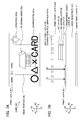
- Fig. 1A and Fig. 1B are a top view and a cross-sectional view of a card 1 of a first embodiment, respectively.
- Fig. 1A is a top view of the card 1 (a view illustrating a front 1a of the card when viewed in the normal direction).
- Fig. 1B is a cross-sectional view of the card 1.
- a horizontal direction X, a longitudinal direction Y, and a vertical direction Z (thickness direction) of the card 1 are described for convenience with reference to the state illustrated in Figs. 1A and 1B , but each direction of the card 1 can be appropriately determined depending on the arrangement.
- a lower side Z1 (lower surface side) of Fig. 1B becomes an upper side
- an upper side Z2 (upper surface side) of Fig. 1B becomes a lower side.
- a configuration of the card in the vertical direction Z in the drawings is illustrated in an exaggerated way to clarify the configuration.
- the card 1 is used as, for example, a cash card of a bank.
- the card 1 includes a card substrate 10, a lower print layer 12, a transparent sheet layer 20, an HS (heat seal) layer 21 (lower adhesive layer), a hologram layer 22 (light diffraction layer), a PC layer 23 (upper adhesive layer), a print sheet layer 30, a magnetic stripe 30a, and an upper print layer 31.
- the transparent sheet layer 20, the HS layer 21, the hologram layer 22, the PC layer 23, the print sheet layer 30, and the upper print layer 31 are laminated in this order from a lower side Z1 to an upper side Z2 (one side) of the card substrate 10.
- the card substrate 10 is a base member of the card 1.
- the card substrate 10 is formed of a resin sheet material such as PET, PET-G, PVC, or PC.
- An outer shape of the card substrate 10 is equal to an outer shape of the card 1.
- a color of an upper surface of the card substrate 10 is black.
- a black may be a color of the card substrate 10 itself or may be a color which is printed on a substrate, the color of which is other than black.
- the lower print layer 12 is provided on a lower surface of the card substrate 10.
- precautions for using the card are printed on the lower print layer 12.
- the transparent sheet layer 20 is a transparent layer on which the hologram layer 22 is provided.
- the card substrate 10 is formed of a resin sheet material such as PET, PET-G, PVC, or PC.
- An outer shape of the transparent sheet layer 20 is equal to the outer shape of the card substrate 10.
- the HS layer 21 is an adhesive layer that bonds the transparent sheet layer 20 and the hologram layer 22 together.
- the HS layer 21 is formed of a thermoplastic adhesive (polyester resin or the like). Since the transparent sheet layer 20 and the hologram layer 22 are bonded each other, the hologram layer 22 will beak if an attempt to peel it off is made. In this manner, even if the hologram layer 22 is illegally peeled off, the peeling will be easily found out, so it is possible to increase the security of the card 1.
- the hologram layer 22 is a light diffraction layer for preventing forgery of the card 1.
- the hologram layer 22 is a layer having a Lippmann type hologram.
- the hologram layer 22 has translucency.
- a hologram image 22a of a building is recorded in the hologram layer 22.
- the Lippmann-type hologram layer 22 is configured by applying a special polymer layer on a film (not illustrated), such as a PET substrate, to form an interference pattern due to changes in refractive index inside the polymer layer.
- the hologram layer 22 reproduces a hologram image via a diffraction phenomenon when light is incident on the interference pattern.
- the hologram layer 22 excels in the presentation of a stereoscopic effect in up and down and left and right directions, and the sense of depth. Accordingly, the hologram layer 22 brings the stereoscopic effect closer to a real object. Since the materials used and production process are unique, forgery of the hologram layer 22 is extremely difficult. Accordingly, the hologram layer 22 is more tolerant of being tampered than an emboss-type hologram, for example.
- An outer shape of the hologram layer 22 is smaller than the outer shape of the card substrate 10, that is, smaller than an outer shape of the transparent sheet layer 20. That is, the hologram layer 22 is laminated only on a partial region of the card substrate 10. The reason for the partial region is to make the expensive hologram layer 22 smaller, resulting in reduced cost.
- the PC layer 23, which is provided on the hologram layer 22, is a layer which bonds the hologram layer 22 and the print sheet layer 30 together.
- An outer shape of the PC layer 23 is equal to the outer shape of the hologram layer 22.
- the PC layer 23 is a thermoplastic resin sheet of PC (polycarbonate) in the embodiments.
- PC polycarbonate
- the type of resin is not limited to PC and may include PET, for example.
- a temperature of the appearance of adhesiveness of the PC layer 23 is higher than that of the HS layer 21.
- the print sheet layer 30 is formed of a resin sheet material such as PET, PET-G, or PVC.
- An upper surface of the print sheet layer 30 may have a mirror-like finish or a matte finish.
- An outer shape of the print sheet layer 30 is similar to the outer shape of the card substrate 10.
- the magnetic stripe 30a is provided on the upper surface of the print sheet layer 30. Information relating to a bank account number or the like is recorded in the magnetic stripe 30a. This information can be read using a reader (not illustrated).
- the magnetic stripe 30a is disposed outside a transition portion 31c (to be described below) of the upper print layer 31.
- the upper print layer 31 is a layer printed in a black color as a background similar to that of the card substrate 10.
- the upper print layer 31 is printed with characters 31a indicating the name of a bank, graphics 31b, or other necessary information (not illustrated).
- the upper print layer 31 has the transition portion 31c.
- the transition portion 31c is a portion of gradation printing in which the color density drops progressively towards inside the gradation printing.
- An outer edge portion 31d of the transition portion 31c is positioned more inside than an edge portion 22b of the hologram layer 22.
- the color density of the transition portion 31c becomes progressively lower, starting from 100% at the outer edge portion 31d to 0% at an inner edge portion 31e.
- a region 31f positioned more outside than the transition portion 31c of the upper print layer 31 has a color density equal or substantially equal to a color density of the card substrate 10.
- a portion positioned more inside than the inner edge portion 31e of the transition portion 31c serves as a window portion 31g.
- the transparent print sheet layer 30 is completely exposed in the window portion 31g. In this manner, an entirety of the hologram image 22a of the hologram layer 22 is visually recognizable through the window portion 31g.
- the upper print layer 31 may alternatively be provided on a lower surface of the print sheet layer 30 if necessary.
- the region 31f positioned more outside than the transition portion 31c of the upper print layer 31 has the color density equal or substantially equal to a color density of the card substrate 10.
- the edge portion 22b of the hologram layer 22 is shielded and hidden by the upper print layer 31 (see an arrow A).
- the card substrate 10 and the upper print layer 31 have a black color or its family, which absorbs light, the edge portion 22b of the hologram layer 22 is hardly recognizable visually.
- the upper print layer 31 and the card substrate 10 have a black color of a similar color family. In this manner, the upper print layer 31 and the card substrate 10 are visually recognized as a single seamless part.
- the hologram image 22a can be confirmed inside the window portion 31g. Since the hologram is a transparent hologram, the color of the card substrate 10 is visually recognized at regions (an external region 22c outside the building, an internal portion 22e inside the building other than a line 22d, and the like) other than the hologram image 22a of the hologram layer 22. In addition, as described above, the upper print layer 31 and the card substrate 10 are visually recognized seamlessly as a single part.
- the circumference of the hologram image 22a is seen to have a wider range of black background surface than the hologram layer 22.
- the hologram image 22a emerges from a black background, and so the hologram image 22a is seen more three-dimensionally.
- the background of the upper print layer 31 is printed in black, the internal part of the card is hidden outside the transition portion 31c.
- the graphic 31b or the like printed on the upper print layer 31 is seen outside the transition portion 31c.
- the magnetic stripe 30a is also hidden.
- the character 31a which is printed to traverse the window portion 31g, is visually recognizable across the window portion 31g, the transition portion 31c, and the outside of the transition portion 31c.
- the character 31a indicating a bank is seen overlapped with the hologram image 22a inside the window portion 31g.
- Fig. 2 is a cross-sectional view of a substrate sheet material 10A, a hologram laminated sheet material 20A, and a print sheet material 30A according to the first embodiment.
- Fig. 3 is a top view of the substrate sheet material 10A, the hologram laminated sheet material 20A, and the print sheet material 30A according to the first embodiment.
- the substrate sheet material 10A, the hologram laminated sheet material 20A, and the print sheet material 30A are sheet materials of multi-face layout having been produced in a previous step prior to a main step.
- Fig. 3 illustrates an example of multi-face layout which is arranged in two rows and five columns.
- the following processes are performed on the sheet material (card substrate 10) obtained by performing black printing on a black resin sheet or a resin sheet of a color other than black.
- a transfer foil provided on the PET is transferred onto a lower side Z1 of the sheet material.
- the substrate sheet material 10A provided with the lower print layer 12 is produced.
- the hologram layer 22 is produced, the PC layer 23 is laminated onto the upper side Z2 of the hologram layer 22, and the HS layer 21 is laminated onto the lower side Z1 of the hologram layer 22.
- the hologram layer 22 laminated in the above step (1) is laminated onto the upper side Z2 of the transparent sheet material (transparent sheet layer 20) by heat sealing (application of heat and pressure).
- a temperature of the heat sealing is set within a temperature range in which the adhesiveness of the HS layer 21 appears but the adhesiveness of the PC layer 23 does not appear.
- the pressurizing plate and the hologram layer 22 do not come in directly contact with each other and thus the hologram layer 22 can be protected.
- the hologram laminated sheet material 20A is produced in which the HS layer 21, the hologram layer 22, and PC layer 23 are laminated onto the upper side Z2 of the sheet material.
- the magnetic stripe 30a is laminated onto an upper surface of the transparent sheet material (print sheet layer 30).
- a transfer foil (upper print layer 31) provided on PET is transferred to an upper surface of the sheet material provided with the magnetic stripe 30a laminated in the above step (1).
- the print sheet material 30A is produced in which the magnetic stripe 30a and the upper print layer 31 are laminated.
- the substrate sheet material 10A, the hologram laminated sheet material 20A, and the print sheet material 30A are processed as follows.
- the substrate sheet material 10A and the hologram laminated sheet material 20A are laminated to each other using thermal welding while being heated and pressurized. These layers may alternatively be bonded each other using an adhesive or the like.
- the print sheet material 30A is then laminated through thermal welding while being heated and pressurized onto the upper side Z2 of the hologram laminated sheet material 20A laminated in the above step (1).
- These layers may alternatively be bonded each other using an adhesive or the like.
- the PC layer 23 is softened by a heat-sealing process, such that the hologram laminated sheet material 20A and the print sheet material 30A are bonded each other. In this case, since the PC layer 23 is softened, it is possible to prevent the hologram from suffering from damage due to the application of a pressure.
- the PC layer 23 is a thermoplastic resin sheet, it is possible to use the PC layer 23 as not only an adhesive layer but also a protection for the hologram layer 22 against the damage due to the application of a pressure.
- the laminated sheet materials 10A, 20A, and 30A are divided into separate pieces with an outer shape of the card by punching.
- the hologram laminated sheet material 20A since the hologram laminated sheet material 20A has been produced in advance in a separate step, it is possible to produce easily the card 1 embedded with the Lippmann hologram by laminating the sheet materials 10A, 20A, and 30A.
- All of steps of producing the card may be performed at a single factory. However, it may be alternatively possible that the previous steps of producing the substrate sheet material 10A, the hologram laminated sheet material 20A, and the print sheet material 30A are performed at a different factory, such that the previous steps and the main step are performed at different factories.
- the hologram laminated sheet material 20A having the hologram layer 22 is produced at a factory having the required technology; the substrate sheet material 10A and the print sheet material 30A are produced at a different factory from the hologram laminated sheet material 20A; and the main step is also performed at a different factory from the hologram laminated sheet material 20A.
- the separate step of producing the hologram laminated sheet material 20A facilitates the production of the card 1 of the present embodiment, which has a Lippmann hologram for which a high technique is required.
- the upper print layer 31 and the card substrate 10 of black have been described as an example, but are not limited thereto.
- the upper print layer 31 and the card substrate 10 may alternatively have any color of a similar color family.
- the color of the card substrate 10 or the upper print layer 31 does not matter as long as the upper print layer 31 has an effect of hiding the edge portion 22b of the hologram layer.
- Fig. 4 is a cross-sectional view (corresponding to Fig. 2 ) of a substrate sheet material 10A, a hologram laminated sheet material 220A, and a print sheet material 30A according to the second embodiment.
- the hologram laminated sheet material 220A is configured so that a PET layer 223 and an HS layer 224 (upper adhesive layer) instead of the PC layer 23 (see Fig. 1B ) are laminated from a lower side Z1 in this order.
- the HS layer 224 bonds the hologram laminated sheet material 20A and the print sheet material 30A by a heat-sealing process. Accordingly, for the same reason as in the first embodiment, a temperature of the appearance of adhesiveness of the HS layer 224 is higher than a temperature of the appearance of adhesiveness of the HS layer 21. That is for creating a condition under which the adhesiveness of the HS layer 21 appears, but the adhesiveness of the HS layer 224 does not appear, when the hologram layer 22 is laminated onto the transparent sheet layer 20 by heat sealing.
- the PET layer 223 can prevent a hologram from suffering from the damage due to the application of a pressure.
- the card of the second embodiment has the same effect as that of the first embodiment.
- Fig. 5A and Fig. 5B are a top view and a cross-sectional view of a card 301 of the third embodiment.
- Fig. 6 is a cross-sectional view of a substrate sheet material 10A and a hologram laminated sheet material 320A of the card 301 according to the third embodiment.
- the card 301 is configured so that a PC layer 23 (see Fig. 1B ) or the like is not provided on a hologram layer 22 and an upper print layer 331 is directly provided on the hologram layer 22.
- a magnetic stripe 30a is provided on a transparent sheet layer 20.
- the hologram laminated sheet material 320A has a simple configuration, accordingly.
- the upper print layer 331 is provided using foil transfer or through a step of printing, such as silk printing.
- the step of printing may be performed at a time of producing the hologram laminated sheet material 320A of the previous step or may be performed in the main step. That is, the hologram laminated sheet material 320A provided previously with the upper print layer 331 may be delivered to a factory in which the main step is performed, or the upper print layer 331 may be provided when each of the sheet materials 10A and 220A is laminated after the delivery at the factory.
- the card 301 of the present embodiment is configured in such a manner that the upper print layer 331 is directly provided on the hologram laminated sheet material 320A.
- the card 301 is configured so that the PC layer 23 (see Fig. 1B ) is provided on the hologram layer 22, similarly with the first embodiment.
- the hologram it is possible to protect the hologram and suppress the damage of the hologram in the steps of heating and applying a pressure, for example, at the time of the production.
- Fig. 7A and Fig. 7B are a top view and a cross-sectional view of a card 401 of the fourth embodiment.
- a card substrate 410 differs from that of the first embodiment in that a print layer 411 is provided.
- Fig. 7A and Fig. 7B illustrate an example in which a name of a card owner is printed on the print layer 411. It is not limited thereto, but it may be alternatively possible that a finer background, micro-printing or the like is provided thereon. Although the description is not presented, the print layer 411 is provided through printing on a substrate sheet material 10A at the time of producing the substrate sheet material 10A (see Fig. 2 ). The card substrate 410 may have any color in place of black.
- An upper print layer 431 is not provided with a transition portion 31c and is printed with only a character 431a, a graphic 431b and the like necessary for the transparent sheet material. That is, a transparent surface is exposed at background regions except for the character 431a and the graphic 431b. Accordingly, the card substrate 410 is visually recognizable (see an arrow C), and an edge portion 22b of a hologram layer 22 is also visually recognizable.
- the card 401 of the fourth embodiment which is configured so that an upper surface of the card substrate 410 and the print layer 411 on the card substrate 410 are visually recognizable, differs from the other embodiments described above.
- the card 401 is suitable for a certificate or the like.
- the configuration of the fourth embodiment is also applicable to the second and third embodiments.
- the present invention is not limited to the above-described embodiments, and may be modified into various forms like the following modified example.
- the modified example will also be included in the technical scope of the present invention.
- the effect of the embodiments is merely the preferred effect obtained from the present invention, and the effect of the present invention is not limited to the effect described in the embodiments.
- the above-described embodiments and the following modified example may be used while being appropriately combined with each other, but a detailed description thereof will not be provided.
Landscapes
- Engineering & Computer Science (AREA)
- Manufacturing & Machinery (AREA)
- Physics & Mathematics (AREA)
- General Physics & Mathematics (AREA)
- Computer Security & Cryptography (AREA)
- Chemical Kinetics & Catalysis (AREA)
- Health & Medical Sciences (AREA)
- Chemical & Material Sciences (AREA)
- Optics & Photonics (AREA)
- General Chemical & Material Sciences (AREA)
- General Health & Medical Sciences (AREA)
- Toxicology (AREA)
- Business, Economics & Management (AREA)
- Accounting & Taxation (AREA)
- Finance (AREA)
- Credit Cards Or The Like (AREA)
- Holo Graphy (AREA)
- Diffracting Gratings Or Hologram Optical Elements (AREA)
Abstract
Description
- The present invention relates to a light diffraction layer laminated sheet and a method for producing a card.
- Hitherto, a card has been known of in which a light diffraction structure is built, such as a hologram (for example, see Patent Document 1).
- However, a high manufacturing technical level was required for existing light diffraction structures, and there were a limited number of manufacturers. Furthermore, when the light diffraction structure is a Lippmann hologram, a higher manufacturing technical level was required and there were a less number of manufacturers.
Patent Document 1: Japanese Unexamined Patent Application, Publication No.2002-32724 - An object of the present invention is to provide a light diffraction layer laminated sheet by which a card having a light diffraction structure can be easily produced, and a card.
- The present invention solves the above-described problems with the following means. Reference numerals corresponding to those of an embodiment of the present invention are given for the sake of better understanding, but it should be noted that the present invention is not limited thereto. Also, the constituents indicated by the reference numerals may be appropriately improved, and at least some of these constituents may be replaced by the other constituents.
- In a first aspect of the invention, a light diffraction layer laminated sheet (20, 20A, 220, 220A, 320, 320A) is provided, which is laminated on an upper side of a card substrate (10, 10A, 410, 410A) to form a part of a laminated structure of a card. The light diffraction layer laminated sheet includes: a transparent sheet layer (20, 20A, 220, 220A, 320, 320A); a light diffraction layer (22) configured to have an outer shape smaller than an outer shape of the transparent sheet layer and to be laminated onto an upper side which is one surface side of the transparent sheet layer; and a lower adhesive layer (21) that bonds the transparent sheet layer and the light diffraction layer together.
- In a second aspect of the invention, the light diffraction layer laminated sheet according to the first aspect is provided, which further includes: a print sheet layer (30, 30A), which has been undergone printing, configured to be laminated onto the light diffraction layer (22); and an upper adhesive layer (23, 224) that is provided on the light diffraction layer, such that the light diffraction layer and the print sheet layer are bonded together.
- In a third aspect of the present invention, the light diffraction layer laminated sheet according to the second aspect is provided, wherein the lower adhesive layer (21) and the upper adhesive layer (23, 224) are thermoplastic members, respectively and the upper adhesive layer is configured to have a higher temperature at which adhesiveness thereof appears than a temperature of the lower adhesive layer at which adhesiveness thereof appears.
- In a fourth aspect of the present invention, the light diffraction layer laminated sheet according to the second or third aspect is provided, wherein the upper adhesive layer (23) includes a thermoplastic resin sheet, and the lower adhesive layer (21) includes a thermoplastic adhesive.
- In a fifth aspect of the present invention, the light diffraction layer laminated sheet according to the first aspect is provided, which further includes a print layer (331) that is directly printed immediately on the light diffraction layer (22).
- In a sixth aspect of the present invention, the light diffraction layer laminated sheet according to any one of the first to fifth aspect is provided, wherein the light diffraction layer (22) includes a Lippmann-type hologram.
- In a seventh aspect of the present invention, a method for producing a card using the light diffraction layer laminated sheet according to any one of the second to fourth aspect is provided, in which the card (1, 301, 401) is produced through a multi-face layout. The method includes steps of: laminating a light diffraction layer laminated sheet material (20A, 220A, 320A), which is laminated with a plurality of light diffraction layers (22), on a substrate sheet material (10A) forming a plurality of card substrates (10, 410); and laminating a print sheet material (30A) forming a plurality of print sheet layers (30) onto the light diffraction layer laminated sheet material.
- In an eighth aspect of the present invention, a method for producing a card using the light diffraction layer laminated sheet according to the fifth aspect is provided, in which the card (301) is produced through a multi-face layout. The method includes steps of: laminating a light diffraction layer laminated sheet material (30A), which is laminated with a plurality of light diffraction layers (22), onto a substrate sheet material (10A) forming a plurality of card substrates (10); and directly printing immediately on the light diffraction layer (22).
- According to the present invention, it is possible to provide a light diffraction layer laminated sheet by which a card having a light diffraction structure can be easily produced, and a card.
-
-
Fig. 1A and Fig. 1B are a top view and a cross-sectional view of a card 1 according to a first embodiment, respectively. -
Fig. 2 is a cross-sectional view of a substrate sheet material 10A, a hologram laminated sheet material 20A, and aprint sheet material 30A according to the first embodiment. -
Fig. 3 is a top view of the substrate sheet material 10A, the hologram laminated sheet material 20A, and theprint sheet material 30A according to the first embodiment. -
Fig. 4 is a cross-sectional view of a substrate sheet material 10A, a hologram laminated sheet material 220A, and aprint sheet material 30A according to a second embodiment. -
Fig. 5A and Fig. 5B are a top view and a cross-sectional view of acard 301 according to a third embodiment, respectively. -
Fig. 6 is a cross-sectional view of a substrate sheet material 10A and a hologram laminatedsheet material 320A of thecard 301 according to the third embodiment. -
Fig. 7A and Fig. 7B are a top view and a cross-sectional view of acard 401 according to a fourth embodiment, respectively. - Hereinafter, embodiments of the present invention will be described with reference to the drawings.
-
Fig. 1A and Fig. 1B are a top view and a cross-sectional view of a card 1 of a first embodiment, respectively. -
Fig. 1A is a top view of the card 1 (a view illustrating afront 1a of the card when viewed in the normal direction). -
Fig. 1B is a cross-sectional view of the card 1. - In the embodiments, a horizontal direction X, a longitudinal direction Y, and a vertical direction Z (thickness direction) of the card 1 are described for convenience with reference to the state illustrated in
Figs. 1A and 1B , but each direction of the card 1 can be appropriately determined depending on the arrangement. For example, when the front and the rear of the card 1 are arranged inversely to the state ofFig. 1B , in the vertical direction Z of the card 1, a lower side Z1 (lower surface side) ofFig. 1B becomes an upper side and an upper side Z2 (upper surface side) ofFig. 1B becomes a lower side. In addition, a configuration of the card in the vertical direction Z in the drawings is illustrated in an exaggerated way to clarify the configuration. - The card 1 is used as, for example, a cash card of a bank.
- The card 1 includes a
card substrate 10, alower print layer 12, a transparent sheet layer 20, an HS (heat seal) layer 21 (lower adhesive layer), a hologram layer 22 (light diffraction layer), a PC layer 23 (upper adhesive layer), a print sheet layer 30, amagnetic stripe 30a, and anupper print layer 31. The transparent sheet layer 20, theHS layer 21, thehologram layer 22, thePC layer 23, the print sheet layer 30, and theupper print layer 31 are laminated in this order from a lower side Z1 to an upper side Z2 (one side) of thecard substrate 10. - The
card substrate 10 is a base member of the card 1. Thecard substrate 10 is formed of a resin sheet material such as PET, PET-G, PVC, or PC. An outer shape of thecard substrate 10 is equal to an outer shape of the card 1. - A color of an upper surface of the
card substrate 10 is black. A black may be a color of thecard substrate 10 itself or may be a color which is printed on a substrate, the color of which is other than black. - The
lower print layer 12 is provided on a lower surface of thecard substrate 10. - For example, precautions for using the card are printed on the
lower print layer 12. - The transparent sheet layer 20 is a transparent layer on which the
hologram layer 22 is provided. Thecard substrate 10 is formed of a resin sheet material such as PET, PET-G, PVC, or PC. An outer shape of the transparent sheet layer 20 is equal to the outer shape of thecard substrate 10. - The
HS layer 21 is an adhesive layer that bonds the transparent sheet layer 20 and thehologram layer 22 together. TheHS layer 21 is formed of a thermoplastic adhesive (polyester resin or the like). Since the transparent sheet layer 20 and thehologram layer 22 are bonded each other, thehologram layer 22 will beak if an attempt to peel it off is made. In this manner, even if thehologram layer 22 is illegally peeled off, the peeling will be easily found out, so it is possible to increase the security of the card 1. - The
hologram layer 22 is a light diffraction layer for preventing forgery of the card 1. Thehologram layer 22 is a layer having a Lippmann type hologram. Thehologram layer 22 has translucency. Ahologram image 22a of a building is recorded in thehologram layer 22. - The Lippmann-
type hologram layer 22 is configured by applying a special polymer layer on a film (not illustrated), such as a PET substrate, to form an interference pattern due to changes in refractive index inside the polymer layer. Thehologram layer 22 reproduces a hologram image via a diffraction phenomenon when light is incident on the interference pattern. Thehologram layer 22 excels in the presentation of a stereoscopic effect in up and down and left and right directions, and the sense of depth. Accordingly, thehologram layer 22 brings the stereoscopic effect closer to a real object. Since the materials used and production process are unique, forgery of thehologram layer 22 is extremely difficult. Accordingly, thehologram layer 22 is more tolerant of being tampered than an emboss-type hologram, for example. - An outer shape of the
hologram layer 22 is smaller than the outer shape of thecard substrate 10, that is, smaller than an outer shape of the transparent sheet layer 20. That is, thehologram layer 22 is laminated only on a partial region of thecard substrate 10. The reason for the partial region is to make theexpensive hologram layer 22 smaller, resulting in reduced cost. - The
PC layer 23, which is provided on thehologram layer 22, is a layer which bonds thehologram layer 22 and the print sheet layer 30 together. An outer shape of thePC layer 23 is equal to the outer shape of thehologram layer 22. ThePC layer 23 is a thermoplastic resin sheet of PC (polycarbonate) in the embodiments. However, the type of resin is not limited to PC and may include PET, for example. - A temperature of the appearance of adhesiveness of the
PC layer 23 is higher than that of theHS layer 21. - The print sheet layer 30 is formed of a resin sheet material such as PET, PET-G, or PVC. An upper surface of the print sheet layer 30 may have a mirror-like finish or a matte finish. An outer shape of the print sheet layer 30 is similar to the outer shape of the
card substrate 10. - The
magnetic stripe 30a is provided on the upper surface of the print sheet layer 30. Information relating to a bank account number or the like is recorded in themagnetic stripe 30a. This information can be read using a reader (not illustrated). - As illustrated in
Fig. 1A , themagnetic stripe 30a is disposed outside atransition portion 31c (to be described below) of theupper print layer 31. - The
upper print layer 31 is a layer printed in a black color as a background similar to that of thecard substrate 10. - In addition, the
upper print layer 31 is printed withcharacters 31a indicating the name of a bank,graphics 31b, or other necessary information (not illustrated). - The
upper print layer 31 has thetransition portion 31c. - The
transition portion 31c is a portion of gradation printing in which the color density drops progressively towards inside the gradation printing. Anouter edge portion 31d of thetransition portion 31c is positioned more inside than anedge portion 22b of thehologram layer 22. - The color density of the
transition portion 31c becomes progressively lower, starting from 100% at theouter edge portion 31d to 0% at aninner edge portion 31e. Aregion 31f positioned more outside than thetransition portion 31c of theupper print layer 31 has a color density equal or substantially equal to a color density of thecard substrate 10. - A portion positioned more inside than the
inner edge portion 31e of thetransition portion 31c serves as awindow portion 31g. - The transparent print sheet layer 30 is completely exposed in the
window portion 31g. In this manner, an entirety of thehologram image 22a of thehologram layer 22 is visually recognizable through thewindow portion 31g. - The
upper print layer 31 may alternatively be provided on a lower surface of the print sheet layer 30 if necessary. - Next, how the card 1 is seen from the upper side Z2 will be described.
- As described above, the
region 31f positioned more outside than thetransition portion 31c of theupper print layer 31 has the color density equal or substantially equal to a color density of thecard substrate 10. In this manner, theedge portion 22b of thehologram layer 22 is shielded and hidden by the upper print layer 31 (see an arrow A). Moreover, since thecard substrate 10 and theupper print layer 31 have a black color or its family, which absorbs light, theedge portion 22b of thehologram layer 22 is hardly recognizable visually. - Only the color of the
upper print layer 31 is visually recognized at theouter edge portion 31d of thetransition portion 31c. Since thehologram layer 22 is transparent, thecard substrate 10 becomes visually recognizable as a horizontal location moves inside from theouter edge portion 31d. Then, only the color of thecard substrate 10 is visually recognizable at theinner edge portion 31e of thetransition portion 31c (see an arrow B). Moreover, theupper print layer 31 and thecard substrate 10 have a black color of a similar color family. In this manner, theupper print layer 31 and thecard substrate 10 are visually recognized as a single seamless part. - Since the
upper print layer 31 is not formed on the print sheet layer 30, thehologram image 22a can be confirmed inside thewindow portion 31g. Since the hologram is a transparent hologram, the color of thecard substrate 10 is visually recognized at regions (anexternal region 22c outside the building, aninternal portion 22e inside the building other than aline 22d, and the like) other than thehologram image 22a of thehologram layer 22. In addition, as described above, theupper print layer 31 and thecard substrate 10 are visually recognized seamlessly as a single part. - For this reason, the circumference of the
hologram image 22a is seen to have a wider range of black background surface than thehologram layer 22. - In this manner, the
hologram image 22a emerges from a black background, and so thehologram image 22a is seen more three-dimensionally. - The visual effect described above has been already confirmed by the production of test samples.
- Since the background of the
upper print layer 31 is printed in black, the internal part of the card is hidden outside thetransition portion 31c. In addition, the graphic 31b or the like printed on theupper print layer 31 is seen outside thetransition portion 31c. Themagnetic stripe 30a is also hidden. - In this connection, the
character 31a, which is printed to traverse thewindow portion 31g, is visually recognizable across thewindow portion 31g, thetransition portion 31c, and the outside of thetransition portion 31c. In this case, thecharacter 31a indicating a bank is seen overlapped with thehologram image 22a inside thewindow portion 31g. - A method for producing a card 1 will be described below.
-
Fig. 2 is a cross-sectional view of a substrate sheet material 10A, a hologram laminated sheet material 20A, and aprint sheet material 30A according to the first embodiment. -
Fig. 3 is a top view of the substrate sheet material 10A, the hologram laminated sheet material 20A, and theprint sheet material 30A according to the first embodiment. - The substrate sheet material 10A, the hologram laminated sheet material 20A, and the
print sheet material 30A are sheet materials of multi-face layout having been produced in a previous step prior to a main step.Fig. 3 illustrates an example of multi-face layout which is arranged in two rows and five columns. - First, a method for producing each of the substrate sheet material 10A, the hologram laminated sheet material 20A, and the
print sheet material 30A will be described. It should be noted that the order of the following steps may be appropriately replaced with each other. - The following processes are performed on the sheet material (card substrate 10) obtained by performing black printing on a black resin sheet or a resin sheet of a color other than black.
- For example, a transfer foil provided on the PET is transferred onto a lower side Z1 of the sheet material.
- Thus, the substrate sheet material 10A provided with the
lower print layer 12 is produced. - As illustrated in
Fig. 2 , thehologram layer 22 is produced, thePC layer 23 is laminated onto the upper side Z2 of thehologram layer 22, and theHS layer 21 is laminated onto the lower side Z1 of thehologram layer 22. - The
hologram layer 22 laminated in the above step (1) is laminated onto the upper side Z2 of the transparent sheet material (transparent sheet layer 20) by heat sealing (application of heat and pressure). A temperature of the heat sealing is set within a temperature range in which the adhesiveness of theHS layer 21 appears but the adhesiveness of thePC layer 23 does not appear. In this case, since thePC layer 23 is interposed between thehologram layer 22 and a pressurizing plate for the heat sealing, the pressurizing plate and thehologram layer 22 do not come in directly contact with each other and thus thehologram layer 22 can be protected. - In this manner, the hologram laminated sheet material 20A is produced in which the
HS layer 21, thehologram layer 22, andPC layer 23 are laminated onto the upper side Z2 of the sheet material. - As illustrated in
Fig. 2 , themagnetic stripe 30a is laminated onto an upper surface of the transparent sheet material (print sheet layer 30). - For example, a transfer foil (upper print layer 31) provided on PET is transferred to an upper surface of the sheet material provided with the
magnetic stripe 30a laminated in the above step (1). - Thus, the
print sheet material 30A is produced in which themagnetic stripe 30a and theupper print layer 31 are laminated. - Next, in the main step, the substrate sheet material 10A, the hologram laminated sheet material 20A, and the
print sheet material 30A are processed as follows. - The substrate sheet material 10A and the hologram laminated sheet material 20A are laminated to each other using thermal welding while being heated and pressurized. These layers may alternatively be bonded each other using an adhesive or the like.
- The
print sheet material 30A is then laminated through thermal welding while being heated and pressurized onto the upper side Z2 of the hologram laminated sheet material 20A laminated in the above step (1). These layers may alternatively be bonded each other using an adhesive or the like. In addition, thePC layer 23 is softened by a heat-sealing process, such that the hologram laminated sheet material 20A and theprint sheet material 30A are bonded each other. In this case, since thePC layer 23 is softened, it is possible to prevent the hologram from suffering from damage due to the application of a pressure. - Since the
PC layer 23 is a thermoplastic resin sheet, it is possible to use thePC layer 23 as not only an adhesive layer but also a protection for thehologram layer 22 against the damage due to the application of a pressure. - The
laminated sheet materials 10A, 20A, and 30A are divided into separate pieces with an outer shape of the card by punching. - With the above-described process, the card 1 has been produced.
- In the present embodiment, since the hologram laminated sheet material 20A has been produced in advance in a separate step, it is possible to produce easily the card 1 embedded with the Lippmann hologram by laminating the
sheet materials 10A, 20A, and 30A. - All of steps of producing the card may be performed at a single factory. However, it may be alternatively possible that the previous steps of producing the substrate sheet material 10A, the hologram laminated sheet material 20A, and the
print sheet material 30A are performed at a different factory, such that the previous steps and the main step are performed at different factories. - Here, an advanced technology is required for the production of the
hologram layer 22. For this reason, it is possible to perform sharing of the steps among factories. For example, the hologram laminated sheet material 20A having thehologram layer 22 is produced at a factory having the required technology; the substrate sheet material 10A and theprint sheet material 30A are produced at a different factory from the hologram laminated sheet material 20A; and the main step is also performed at a different factory from the hologram laminated sheet material 20A. - As a result of sharing of the steps, it is possible for a factory performing the main step to produce the card 1 of an end product as long as the hologram laminated sheet material 20A is available, even if the factory performing the main step does not have the technology for producing a Lippmann hologram. That is, since the card-producing step has a separate step of producing the hologram laminated sheet material 20A, it is possible to easily produce a card with the Lippmann hologram. Accordingly, this will increase the number of factories at which it is possible to produce the card 1 with the Lippmann hologram, and will contribute to the expansion of the market.
- Even if the steps are shared as described above, it is possible to protect the
hologram layer 22 since the hologram laminated sheet material 20A has thePC layer 23. Accordingly, the storage and handling during transportation are easy. - As described above, the separate step of producing the hologram laminated sheet material 20A facilitates the production of the card 1 of the present embodiment, which has a Lippmann hologram for which a high technique is required.
- The
upper print layer 31 and thecard substrate 10 of black have been described as an example, but are not limited thereto. For example, theupper print layer 31 and thecard substrate 10 may alternatively have any color of a similar color family. In addition, the color of thecard substrate 10 or theupper print layer 31 does not matter as long as theupper print layer 31 has an effect of hiding theedge portion 22b of the hologram layer. - A second embodiment of the present invention will be described below.
- It should be noted that, in the description and drawings for the following embodiments, the same reference symbol or the same reference symbol at the end (last two digits) is assigned to a portion which performs a function similarly with the first embodiment described above, and duplicated descriptions are not presented on a case-by-case basis.
-
Fig. 4 is a cross-sectional view (corresponding toFig. 2 ) of a substrate sheet material 10A, a hologram laminated sheet material 220A, and aprint sheet material 30A according to the second embodiment. - The hologram laminated sheet material 220A is configured so that a
PET layer 223 and an HS layer 224 (upper adhesive layer) instead of the PC layer 23 (seeFig. 1B ) are laminated from a lower side Z1 in this order. - In a step of laminating print sheet material of a main step of producing a card, the
HS layer 224 bonds the hologram laminated sheet material 20A and theprint sheet material 30A by a heat-sealing process. Accordingly, for the same reason as in the first embodiment, a temperature of the appearance of adhesiveness of theHS layer 224 is higher than a temperature of the appearance of adhesiveness of theHS layer 21. That is for creating a condition under which the adhesiveness of theHS layer 21 appears, but the adhesiveness of theHS layer 224 does not appear, when thehologram layer 22 is laminated onto the transparent sheet layer 20 by heat sealing. - In addition, the
PET layer 223 can prevent a hologram from suffering from the damage due to the application of a pressure. - In this manner, since the
PET layer 223 and theHS layer 224 function similarly to thePC layer 23 of the first embodiment, the card of the second embodiment has the same effect as that of the first embodiment. - A third embodiment of the present invention will be described below.
-
Fig. 5A and Fig. 5B are a top view and a cross-sectional view of acard 301 of the third embodiment. -
Fig. 6 is a cross-sectional view of a substrate sheet material 10A and a hologram laminatedsheet material 320A of thecard 301 according to the third embodiment. - As illustrated in
Fig. 5B , thecard 301 is configured so that a PC layer 23 (seeFig. 1B ) or the like is not provided on ahologram layer 22 and anupper print layer 331 is directly provided on thehologram layer 22. In addition, amagnetic stripe 30a is provided on a transparent sheet layer 20. - As illustrated in
Fig. 6 , the hologram laminatedsheet material 320A has a simple configuration, accordingly. - The
upper print layer 331 is provided using foil transfer or through a step of printing, such as silk printing. - The step of printing may be performed at a time of producing the hologram laminated
sheet material 320A of the previous step or may be performed in the main step. That is, the hologram laminatedsheet material 320A provided previously with theupper print layer 331 may be delivered to a factory in which the main step is performed, or theupper print layer 331 may be provided when each of the sheet materials 10A and 220A is laminated after the delivery at the factory. - As described above, the
card 301 of the present embodiment is configured in such a manner that theupper print layer 331 is directly provided on the hologram laminatedsheet material 320A. - Accordingly, it is possible to introduce a simple configuration, which results in low cost. In this connection, it may be alternatively possible that the
card 301 is configured so that the PC layer 23 (seeFig. 1B ) is provided on thehologram layer 22, similarly with the first embodiment. In this case, as in the first embodiment, it is possible to protect the hologram and suppress the damage of the hologram in the steps of heating and applying a pressure, for example, at the time of the production. - A fourth embodiment of the present invention will be described below.
-
Fig. 7A and Fig. 7B are a top view and a cross-sectional view of acard 401 of the fourth embodiment. - A card substrate 410 differs from that of the first embodiment in that a
print layer 411 is provided. -
Fig. 7A and Fig. 7B illustrate an example in which a name of a card owner is printed on theprint layer 411. It is not limited thereto, but it may be alternatively possible that a finer background, micro-printing or the like is provided thereon. Although the description is not presented, theprint layer 411 is provided through printing on a substrate sheet material 10A at the time of producing the substrate sheet material 10A (seeFig. 2 ). The card substrate 410 may have any color in place of black. - An
upper print layer 431 is not provided with atransition portion 31c and is printed with only acharacter 431a, a graphic 431b and the like necessary for the transparent sheet material. That is, a transparent surface is exposed at background regions except for thecharacter 431a and the graphic 431b. Accordingly, the card substrate 410 is visually recognizable (see an arrow C), and anedge portion 22b of ahologram layer 22 is also visually recognizable. - As described above, the
card 401 of the fourth embodiment, which is configured so that an upper surface of the card substrate 410 and theprint layer 411 on the card substrate 410 are visually recognizable, differs from the other embodiments described above. For example, when a photograph of card owner's face is provided on theprint layer 411, thecard 401 is suitable for a certificate or the like. - The configuration of the fourth embodiment is also applicable to the second and third embodiments.
- While the embodiments of the present invention have been described, the present invention is not limited to the above-described embodiments, and may be modified into various forms like the following modified example. The modified example will also be included in the technical scope of the present invention. Also, the effect of the embodiments is merely the preferred effect obtained from the present invention, and the effect of the present invention is not limited to the effect described in the embodiments. Furthermore, the above-described embodiments and the following modified example may be used while being appropriately combined with each other, but a detailed description thereof will not be provided.
- (1) In the embodiments, the example has been illustrated in which the hologram layer is a Lippmann type hologram, but it is not limited thereto. For example, the hologram layer may alternatively be an emboss type hologram.
- (2) In the embodiments, the example has been illustrated in which the transition portion does not overlap with the image portion of the hologram, but is not limited thereto. The transition portion may overlap with the image portion of the hologram and may be configured to have a less dense color as the transition portion reaches more inside the image portion. In this case, the image is seen in such a manner that the image is blurred at a periphery thereof and becomes sharper as reaching inside by the transition portion.
- (3) In the embodiments, the example has been illustrated in which the card has the hologram layer, but is not limited thereto. For example, the card may be used in cash vouchers or the like.
- (4) In the embodiments, the example has been illustrated in which the card is produced with the multi-face layout using the sheet materials, but is not limited thereto. The card may alternatively be produced in the form of a single body. In this case, sheet materials constituting a single card may be laminated. In this case, the transparent sheet layer itself laminated with one hologram layer may be used as the hologram laminated sheet material laminated with one hologram layer.
- (5) In the embodiments, the example has been illustrated in which the printing is performed on the card substrate in the range not overlapping the hologram layer, but is not limited thereto. When the printing is performed on the card substrate so as to overlap the hologram layer, the hologram image and the printing are observed overlapped, thereby improving the design. Furthermore, in this case, it is possible to increase security since forgery becomes difficult.
-
- 1, 301, 401 CARD
- 10, 410 card substrate
- 10A substrate sheet material
- 12 lower print layer
- 20 transparent sheet layer
- 20A, 220A, 320A hologram laminated sheet material
- 21 HS layer
- 22 hologram layer
- 23 PC layer
- 30 print sheet layer
- 30a magnetic stripe
- 30A print sheet material
- 31, 331, 431 upper print layer
- 31c transition portion
- 31g window portion
- 223 PET layer
- 224 HS layer
Claims (8)
- A light diffraction layer laminated sheet that is laminated on an upper side of a card substrate to form a part of a laminated structure of a card, comprising:a transparent sheet layer;a light diffraction layer configured to have an outer shape smaller than an outer shape of the transparent sheet layer and to be laminated onto an upper side which is one surface side of the transparent sheet layer; anda lower adhesive layer that bonds the transparent sheet layer and the light diffraction layer together.
- The light diffraction layer laminated sheet according to claim 1, further comprising:a print sheet layer, which has been undergone printing, configured to be laminated onto the light diffraction layer; andan upper adhesive layer that is provided on the light diffraction layer, such that the light diffraction layer and the print sheet layer are bonded together.
- The light diffraction layer laminated sheet according to claim 2,
wherein the lower adhesive layer and the upper adhesive layer are thermoplastic members, respectively and the upper adhesive layer is configured to have a higher temperature at which adhesiveness thereof appears than a temperature of the lower adhesive layer at which adhesiveness thereof appears. - The light diffraction layer laminated sheet according to claim 2 or 3,
wherein the upper adhesive layer comprises a thermoplastic resin sheet, and
the lower adhesive layer comprises a thermoplastic adhesive. - The light diffraction layer laminated sheet according to claim 1, further comprising a print layer that is directly printed immediately on the light diffraction layer.
- The light diffraction layer laminated sheet according to any one of claims 1 to 5,
wherein the light diffraction layer comprises a Lippmann-type hologram. - A method for producing a card using the light diffraction layer laminated sheet according to any one of claims 2 to 4,
wherein the card is produced through a multi-face layout and the method comprising steps of:laminating a light diffraction layer laminated sheet material, which is laminated with a plurality of light diffraction layers, on a substrate sheet material forming a plurality of card substrates; andlaminating a print sheet material forming a plurality of print sheet layers onto the light diffraction layer laminated sheet material. - A method for producing a card using the light diffraction layer laminated sheet according to claim 5,
wherein the card is produced through a multi-face layout and the method comprising steps of:laminating a light diffraction layer laminated sheet material, which is laminated with a plurality of light diffraction layers, onto a substrate sheet material forming a plurality of card substrates; anddirectly printing immediately on the light diffraction layer.
Priority Applications (3)
| Application Number | Priority Date | Filing Date | Title |
|---|---|---|---|
| EP23220571.6A EP4328671A3 (en) | 2012-11-13 | 2013-11-12 | Light diffraction layer laminated sheet and method for producing card |
| EP17188126.1A EP3270231B1 (en) | 2012-11-13 | 2013-11-12 | Light diffraction layer laminated sheet and method for producing card |
| EP19195171.4A EP3597445B1 (en) | 2012-11-13 | 2013-11-12 | Light diffraction layer laminated sheet and method for producing card |
Applications Claiming Priority (2)
| Application Number | Priority Date | Filing Date | Title |
|---|---|---|---|
| JP2012249650A JP6273669B2 (en) | 2012-11-13 | 2012-11-13 | Optical diffraction layer laminate sheet, card manufacturing method |
| PCT/JP2013/080608 WO2014077256A1 (en) | 2012-11-13 | 2013-11-12 | Light diffraction layer laminated sheet and method for producing card |
Related Child Applications (3)
| Application Number | Title | Priority Date | Filing Date |
|---|---|---|---|
| EP17188126.1A Division EP3270231B1 (en) | 2012-11-13 | 2013-11-12 | Light diffraction layer laminated sheet and method for producing card |
| EP19195171.4A Division EP3597445B1 (en) | 2012-11-13 | 2013-11-12 | Light diffraction layer laminated sheet and method for producing card |
| EP23220571.6A Division EP4328671A3 (en) | 2012-11-13 | 2013-11-12 | Light diffraction layer laminated sheet and method for producing card |
Publications (3)
| Publication Number | Publication Date |
|---|---|
| EP2921914A1 true EP2921914A1 (en) | 2015-09-23 |
| EP2921914A4 EP2921914A4 (en) | 2016-06-15 |
| EP2921914B1 EP2921914B1 (en) | 2017-09-27 |
Family
ID=50731168
Family Applications (4)
| Application Number | Title | Priority Date | Filing Date |
|---|---|---|---|
| EP17188126.1A Active EP3270231B1 (en) | 2012-11-13 | 2013-11-12 | Light diffraction layer laminated sheet and method for producing card |
| EP19195171.4A Active EP3597445B1 (en) | 2012-11-13 | 2013-11-12 | Light diffraction layer laminated sheet and method for producing card |
| EP23220571.6A Pending EP4328671A3 (en) | 2012-11-13 | 2013-11-12 | Light diffraction layer laminated sheet and method for producing card |
| EP13854849.0A Active EP2921914B1 (en) | 2012-11-13 | 2013-11-12 | Card with light diffraction layer laminated sheet and method for producing the card |
Family Applications Before (3)
| Application Number | Title | Priority Date | Filing Date |
|---|---|---|---|
| EP17188126.1A Active EP3270231B1 (en) | 2012-11-13 | 2013-11-12 | Light diffraction layer laminated sheet and method for producing card |
| EP19195171.4A Active EP3597445B1 (en) | 2012-11-13 | 2013-11-12 | Light diffraction layer laminated sheet and method for producing card |
| EP23220571.6A Pending EP4328671A3 (en) | 2012-11-13 | 2013-11-12 | Light diffraction layer laminated sheet and method for producing card |
Country Status (5)
| Country | Link |
|---|---|
| US (2) | US20160282810A1 (en) |
| EP (4) | EP3270231B1 (en) |
| JP (1) | JP6273669B2 (en) |
| FI (2) | FI3270231T3 (en) |
| WO (1) | WO2014077256A1 (en) |
Cited By (1)
| Publication number | Priority date | Publication date | Assignee | Title |
|---|---|---|---|---|
| EP3738784B1 (en) | 2018-01-09 | 2021-10-06 | Toppan Printing Co., Ltd. | Laminate, certificate, and method of manufacturing laminate |
Families Citing this family (2)
| Publication number | Priority date | Publication date | Assignee | Title |
|---|---|---|---|---|
| US8567679B1 (en) | 2011-01-23 | 2013-10-29 | Dynamics Inc. | Cards and devices with embedded holograms |
| EP3045307B1 (en) * | 2014-09-12 | 2019-11-06 | Andrews & Wykeham Limited | Laminated credential |
Citations (2)
| Publication number | Priority date | Publication date | Assignee | Title |
|---|---|---|---|---|
| EP1702766A1 (en) * | 2003-12-24 | 2006-09-20 | Dai Nippon Printing Co., Ltd. | Thermal transfer sheet, method for producing same, and image formed body to which such thermal transfer sheet is transferred |
| WO2012118170A1 (en) * | 2011-03-03 | 2012-09-07 | 大日本印刷株式会社 | Laminated body having hologram |
Family Cites Families (33)
| Publication number | Priority date | Publication date | Assignee | Title |
|---|---|---|---|---|
| JPH0685102B2 (en) | 1985-01-31 | 1994-10-26 | 大日本印刷株式会社 | Card with hologram |
| EP0609683A1 (en) | 1985-05-07 | 1994-08-10 | Dai Nippon Insatsu Kabushiki Kaisha | Relief hologram and process for producing a relief hologram |
| US4988151A (en) | 1989-08-31 | 1991-01-29 | Hughes Aircraft Company | Method for making edge faded holograms |
| US5267753A (en) * | 1991-07-08 | 1993-12-07 | Ernest Chock | Holographic bank draft |
| DE69415547T2 (en) | 1993-09-28 | 1999-08-19 | Minnesota Mining And Mfg. Co. | SECURITY CARD AND THEIR PRODUCTION PROCESS |
| JP3321939B2 (en) * | 1993-11-29 | 2002-09-09 | 凸版印刷株式会社 | Securities and lottery tickets |
| EP2251209A3 (en) * | 1996-09-19 | 2011-11-23 | Dai Nippon Printing Co., Ltd. | Multilayered volume hologram structure, and label for making multilayered volume hologram structure |
| AUPO260296A0 (en) | 1996-09-26 | 1996-10-24 | Reserve Bank Of Australia | Banknotes incorporating security devices |
| JP4286942B2 (en) | 1998-12-08 | 2009-07-01 | 大日本印刷株式会社 | Hologram composite |
| AUPP931399A0 (en) | 1999-03-16 | 1999-04-15 | Documotion Research, Inc. | Improved tamper-evident form |
| EP1169179B2 (en) * | 1999-04-07 | 2012-11-14 | Trüb AG | Data carrier and method for producing same |
| US6581839B1 (en) | 1999-09-07 | 2003-06-24 | American Express Travel Related Services Company, Inc. | Transaction card |
| JP4357670B2 (en) | 1999-10-22 | 2009-11-04 | 大日本印刷株式会社 | Rewritable card |
| DE10007916A1 (en) | 2000-02-21 | 2001-08-23 | Giesecke & Devrient Gmbh | Multilayer laminated card with interposed security element having relief structures |
| DE10013410B4 (en) | 2000-03-17 | 2011-05-05 | Ovd Kinegram Ag | Laminate, in particular in the form of cards, and process for its production |
| JP2001293982A (en) | 2000-04-12 | 2001-10-23 | Dainippon Printing Co Ltd | Information recording medium and information recording card |
| JP4683597B2 (en) | 2000-06-23 | 2011-05-18 | 大日本印刷株式会社 | Hologram transfer foil |
| JP4580517B2 (en) | 2000-07-14 | 2010-11-17 | 大日本印刷株式会社 | Information recording body having light diffraction structure, sheet for attaching light diffraction structure, light diffraction structure transfer sheet, and method for producing information recording body. |
| JP4620280B2 (en) * | 2001-04-16 | 2011-01-26 | 大日本印刷株式会社 | Authenticable card |
| JP4105465B2 (en) | 2002-03-28 | 2008-06-25 | 株式会社サトー | label |
| AUPS221002A0 (en) | 2002-05-09 | 2002-06-06 | Securency Pty Ltd | Security document with biometric or photographic image |
| US20040144472A1 (en) * | 2003-01-24 | 2004-07-29 | G & D Cardtech, Inc. | Process for manufacturing laminated plastic products |
| JP4373169B2 (en) | 2003-09-30 | 2009-11-25 | 大日本印刷株式会社 | Transparent card |
| JP4225143B2 (en) * | 2003-07-17 | 2009-02-18 | 富士ゼロックス株式会社 | Information recording medium, manufacturing method thereof, and information recording medium manufacturing apparatus used in the manufacturing method |
| GB0409736D0 (en) | 2004-04-30 | 2004-06-09 | Rue De Int Ltd | Improvements in substrates incorporating security device |
| EP1744878B1 (en) | 2004-05-06 | 2015-04-22 | Giesecke & Devrient GmbH | Laminated card composite |
| JP4753152B2 (en) | 2005-07-06 | 2011-08-24 | 大日本印刷株式会社 | Transparent card with hologram and transparent card recognition device with hologram |
| JP4816895B2 (en) * | 2005-10-11 | 2011-11-16 | 凸版印刷株式会社 | Magnetic transfer sheet and magnetic recording medium |
| DE102006029397A1 (en) | 2006-06-27 | 2008-01-03 | Ovd Kinegram Ag | Method for producing a laminated layer composite, laminated layer composite and its use |
| JP3131943U (en) * | 2006-12-28 | 2007-05-31 | 森本 桂一郎 | Hologram printed matter and jewelry using the same |
| CA2786796C (en) | 2010-01-19 | 2019-02-19 | Nobuko Oikawa | Volume hologram sheet to be embedded, forgery prevention paper, and card |
| DE102010033049A1 (en) | 2010-08-02 | 2012-02-02 | Bundesdruckerei Gmbh | Adhesive layer for the connection of a holographic data carrier with a substrate |
| JP6107137B2 (en) | 2010-10-15 | 2017-04-05 | 大日本印刷株式会社 | Information recording medium and printing method of information recording medium |
-
2012
- 2012-11-13 JP JP2012249650A patent/JP6273669B2/en active Active
-
2013
- 2013-11-12 EP EP17188126.1A patent/EP3270231B1/en active Active
- 2013-11-12 EP EP19195171.4A patent/EP3597445B1/en active Active
- 2013-11-12 WO PCT/JP2013/080608 patent/WO2014077256A1/en active Application Filing
- 2013-11-12 US US14/442,313 patent/US20160282810A1/en not_active Abandoned
- 2013-11-12 FI FIEP17188126.1T patent/FI3270231T3/en active
- 2013-11-12 EP EP23220571.6A patent/EP4328671A3/en active Pending
- 2013-11-12 EP EP13854849.0A patent/EP2921914B1/en active Active
- 2013-11-12 FI FIEP19195171.4T patent/FI3597445T3/en active
-
2020
- 2020-05-28 US US16/885,857 patent/US11934148B2/en active Active
Patent Citations (2)
| Publication number | Priority date | Publication date | Assignee | Title |
|---|---|---|---|---|
| EP1702766A1 (en) * | 2003-12-24 | 2006-09-20 | Dai Nippon Printing Co., Ltd. | Thermal transfer sheet, method for producing same, and image formed body to which such thermal transfer sheet is transferred |
| WO2012118170A1 (en) * | 2011-03-03 | 2012-09-07 | 大日本印刷株式会社 | Laminated body having hologram |
Non-Patent Citations (2)
| Title |
|---|
| None * |
| See also references of WO2014077256A1 * |
Cited By (2)
| Publication number | Priority date | Publication date | Assignee | Title |
|---|---|---|---|---|
| EP3738784B1 (en) | 2018-01-09 | 2021-10-06 | Toppan Printing Co., Ltd. | Laminate, certificate, and method of manufacturing laminate |
| EP3929002B1 (en) | 2018-01-09 | 2023-08-23 | Toppan Printing Co., Ltd. | Laminate, verification, and method of producing laminate |
Also Published As
| Publication number | Publication date |
|---|---|
| JP6273669B2 (en) | 2018-02-07 |
| EP3597445B1 (en) | 2024-01-17 |
| EP2921914A4 (en) | 2016-06-15 |
| EP2921914B1 (en) | 2017-09-27 |
| FI3270231T3 (en) | 2023-02-19 |
| EP3270231A1 (en) | 2018-01-17 |
| EP3597445A1 (en) | 2020-01-22 |
| FI3597445T3 (en) | 2024-03-14 |
| US11934148B2 (en) | 2024-03-19 |
| EP3270231B1 (en) | 2022-12-14 |
| EP4328671A2 (en) | 2024-02-28 |
| JP2014098770A (en) | 2014-05-29 |
| US20160282810A1 (en) | 2016-09-29 |
| WO2014077256A1 (en) | 2014-05-22 |
| US20200292988A1 (en) | 2020-09-17 |
| EP4328671A3 (en) | 2024-05-01 |
Similar Documents
| Publication | Publication Date | Title |
|---|---|---|
| US11934148B2 (en) | Light diffraction layer laminated sheet and method for producing card | |
| US9174401B2 (en) | Method for producing a multilayer data carrier and data carrier produced by said method | |
| TR201814983T4 (en) | Secure identification document and method of producing it. | |
| JP6477682B2 (en) | Card, card manufacturing method | |
| CN107466382B (en) | Security element with pattern and double-sided holographic effect | |
| CN109733030B (en) | High-security certificate card and manufacturing method thereof | |
| US11305514B2 (en) | Laminate, verification, and method of producing laminate | |
| JP2007003673A (en) | Forgery prevention medium, forgery prevention body used for the same and forgery prevention body transfer foil | |
| CN112469572A (en) | Method for producing a security element having two security features and use of the method | |
| WO2014126025A1 (en) | Light diffraction layer laminated sheet, method for producing light diffraction layer laminated sheet, and method for producing card | |
| CN107206830B (en) | Valuable or safety product and for using non-central individual character manufacturing is valuable or the method for safety product | |
| JP6175792B2 (en) | Optical diffraction layer laminate sheet, card manufacturing method | |
| JP6610620B2 (en) | card | |
| JP2020024457A (en) | Card and method for manufacturing card | |
| JP6460167B2 (en) | Optical diffraction layer laminate sheet, card manufacturing method | |
| JP6413239B2 (en) | Optical diffraction layer laminate sheet, optical diffraction layer laminate, and card manufacturing method | |
| JP6167521B2 (en) | Optical diffraction layer laminate sheet, card manufacturing method | |
| JP6136333B2 (en) | Optical diffraction layer laminate sheet, optical diffraction layer laminate sheet manufacturing method, card manufacturing method | |
| WO2014109316A1 (en) | Light diffraction layer laminated sheet, light diffraction layer laminated body, and method for producing card | |
| JP5169700B2 (en) | Black card with hidden print layer | |
| CN1737825A (en) | Optically variable tamper evident device | |
| JP2014079987A (en) | Card with potting seal |
Legal Events
| Date | Code | Title | Description |
|---|---|---|---|
| PUAI | Public reference made under article 153(3) epc to a published international application that has entered the european phase |
Free format text: ORIGINAL CODE: 0009012 |
|
| 17P | Request for examination filed |
Effective date: 20150521 |
|
| AK | Designated contracting states |
Kind code of ref document: A1 Designated state(s): AL AT BE BG CH CY CZ DE DK EE ES FI FR GB GR HR HU IE IS IT LI LT LU LV MC MK MT NL NO PL PT RO RS SE SI SK SM TR |
|
| AX | Request for extension of the european patent |
Extension state: BA ME |
|
| DAX | Request for extension of the european patent (deleted) | ||
| RA4 | Supplementary search report drawn up and despatched (corrected) |
Effective date: 20160519 |
|
| RIC1 | Information provided on ipc code assigned before grant |
Ipc: B42D 25/351 20140101ALI20160512BHEP Ipc: G02B 5/18 20060101ALI20160512BHEP Ipc: B42D 25/47 20140101ALI20160512BHEP Ipc: B42D 25/328 20140101ALI20160512BHEP Ipc: B42D 25/369 20140101ALI20160512BHEP Ipc: B42D 25/475 20140101ALI20160512BHEP Ipc: G03H 1/02 20060101AFI20160512BHEP Ipc: B42D 25/324 20140101ALI20160512BHEP |
|
| GRAP | Despatch of communication of intention to grant a patent |
Free format text: ORIGINAL CODE: EPIDOSNIGR1 |
|
| STAA | Information on the status of an ep patent application or granted ep patent |
Free format text: STATUS: GRANT OF PATENT IS INTENDED |
|
| INTG | Intention to grant announced |
Effective date: 20170425 |
|
| GRAS | Grant fee paid |
Free format text: ORIGINAL CODE: EPIDOSNIGR3 |
|
| GRAA | (expected) grant |
Free format text: ORIGINAL CODE: 0009210 |
|
| STAA | Information on the status of an ep patent application or granted ep patent |
Free format text: STATUS: THE PATENT HAS BEEN GRANTED |
|
| AK | Designated contracting states |
Kind code of ref document: B1 Designated state(s): AL AT BE BG CH CY CZ DE DK EE ES FI FR GB GR HR HU IE IS IT LI LT LU LV MC MK MT NL NO PL PT RO RS SE SI SK SM TR |
|
| REG | Reference to a national code |
Ref country code: GB Ref legal event code: FG4D |
|
| REG | Reference to a national code |
Ref country code: CH Ref legal event code: EP |
|
| REG | Reference to a national code |
Ref country code: AT Ref legal event code: REF Ref document number: 932516 Country of ref document: AT Kind code of ref document: T Effective date: 20171015 |
|
| REG | Reference to a national code |
Ref country code: FR Ref legal event code: PLFP Year of fee payment: 5 |
|
| REG | Reference to a national code |
Ref country code: IE Ref legal event code: FG4D |
|
| REG | Reference to a national code |
Ref country code: CH Ref legal event code: NV Representative=s name: KATZAROV S.A., CH |
|
| REG | Reference to a national code |
Ref country code: DE Ref legal event code: R096 Ref document number: 602013027310 Country of ref document: DE |
|
| PG25 | Lapsed in a contracting state [announced via postgrant information from national office to epo] |
Ref country code: SE Free format text: LAPSE BECAUSE OF FAILURE TO SUBMIT A TRANSLATION OF THE DESCRIPTION OR TO PAY THE FEE WITHIN THE PRESCRIBED TIME-LIMIT Effective date: 20170927 Ref country code: HR Free format text: LAPSE BECAUSE OF FAILURE TO SUBMIT A TRANSLATION OF THE DESCRIPTION OR TO PAY THE FEE WITHIN THE PRESCRIBED TIME-LIMIT Effective date: 20170927 Ref country code: LT Free format text: LAPSE BECAUSE OF FAILURE TO SUBMIT A TRANSLATION OF THE DESCRIPTION OR TO PAY THE FEE WITHIN THE PRESCRIBED TIME-LIMIT Effective date: 20170927 Ref country code: NO Free format text: LAPSE BECAUSE OF FAILURE TO SUBMIT A TRANSLATION OF THE DESCRIPTION OR TO PAY THE FEE WITHIN THE PRESCRIBED TIME-LIMIT Effective date: 20171227 |
|
| REG | Reference to a national code |
Ref country code: LT Ref legal event code: MG4D |
|
| REG | Reference to a national code |
Ref country code: AT Ref legal event code: MK05 Ref document number: 932516 Country of ref document: AT Kind code of ref document: T Effective date: 20170927 |
|
| PG25 | Lapsed in a contracting state [announced via postgrant information from national office to epo] |
Ref country code: LV Free format text: LAPSE BECAUSE OF FAILURE TO SUBMIT A TRANSLATION OF THE DESCRIPTION OR TO PAY THE FEE WITHIN THE PRESCRIBED TIME-LIMIT Effective date: 20170927 Ref country code: BG Free format text: LAPSE BECAUSE OF FAILURE TO SUBMIT A TRANSLATION OF THE DESCRIPTION OR TO PAY THE FEE WITHIN THE PRESCRIBED TIME-LIMIT Effective date: 20171227 Ref country code: GR Free format text: LAPSE BECAUSE OF FAILURE TO SUBMIT A TRANSLATION OF THE DESCRIPTION OR TO PAY THE FEE WITHIN THE PRESCRIBED TIME-LIMIT Effective date: 20171228 Ref country code: RS Free format text: LAPSE BECAUSE OF FAILURE TO SUBMIT A TRANSLATION OF THE DESCRIPTION OR TO PAY THE FEE WITHIN THE PRESCRIBED TIME-LIMIT Effective date: 20170927 |
|
| REG | Reference to a national code |
Ref country code: CH Ref legal event code: PCAR Free format text: NEW ADDRESS: AVENUE DES MORGINES 12, 1213 PETIT-LANCY (CH) |
|
| PG25 | Lapsed in a contracting state [announced via postgrant information from national office to epo] |
Ref country code: CZ Free format text: LAPSE BECAUSE OF FAILURE TO SUBMIT A TRANSLATION OF THE DESCRIPTION OR TO PAY THE FEE WITHIN THE PRESCRIBED TIME-LIMIT Effective date: 20170927 Ref country code: ES Free format text: LAPSE BECAUSE OF FAILURE TO SUBMIT A TRANSLATION OF THE DESCRIPTION OR TO PAY THE FEE WITHIN THE PRESCRIBED TIME-LIMIT Effective date: 20170927 Ref country code: RO Free format text: LAPSE BECAUSE OF FAILURE TO SUBMIT A TRANSLATION OF THE DESCRIPTION OR TO PAY THE FEE WITHIN THE PRESCRIBED TIME-LIMIT Effective date: 20170927 |
|
| PG25 | Lapsed in a contracting state [announced via postgrant information from national office to epo] |
Ref country code: IT Free format text: LAPSE BECAUSE OF FAILURE TO SUBMIT A TRANSLATION OF THE DESCRIPTION OR TO PAY THE FEE WITHIN THE PRESCRIBED TIME-LIMIT Effective date: 20170927 Ref country code: IS Free format text: LAPSE BECAUSE OF FAILURE TO SUBMIT A TRANSLATION OF THE DESCRIPTION OR TO PAY THE FEE WITHIN THE PRESCRIBED TIME-LIMIT Effective date: 20180127 Ref country code: SK Free format text: LAPSE BECAUSE OF FAILURE TO SUBMIT A TRANSLATION OF THE DESCRIPTION OR TO PAY THE FEE WITHIN THE PRESCRIBED TIME-LIMIT Effective date: 20170927 Ref country code: AT Free format text: LAPSE BECAUSE OF FAILURE TO SUBMIT A TRANSLATION OF THE DESCRIPTION OR TO PAY THE FEE WITHIN THE PRESCRIBED TIME-LIMIT Effective date: 20170927 Ref country code: SM Free format text: LAPSE BECAUSE OF FAILURE TO SUBMIT A TRANSLATION OF THE DESCRIPTION OR TO PAY THE FEE WITHIN THE PRESCRIBED TIME-LIMIT Effective date: 20170927 Ref country code: EE Free format text: LAPSE BECAUSE OF FAILURE TO SUBMIT A TRANSLATION OF THE DESCRIPTION OR TO PAY THE FEE WITHIN THE PRESCRIBED TIME-LIMIT Effective date: 20170927 |
|
| REG | Reference to a national code |
Ref country code: DE Ref legal event code: R026 Ref document number: 602013027310 Country of ref document: DE |
|
| PG25 | Lapsed in a contracting state [announced via postgrant information from national office to epo] |
Ref country code: MC Free format text: LAPSE BECAUSE OF FAILURE TO SUBMIT A TRANSLATION OF THE DESCRIPTION OR TO PAY THE FEE WITHIN THE PRESCRIBED TIME-LIMIT Effective date: 20170927 |
|
| PLBI | Opposition filed |
Free format text: ORIGINAL CODE: 0009260 |
|
| PLAX | Notice of opposition and request to file observation + time limit sent |
Free format text: ORIGINAL CODE: EPIDOSNOBS2 |
|
| PG25 | Lapsed in a contracting state [announced via postgrant information from national office to epo] |
Ref country code: DK Free format text: LAPSE BECAUSE OF FAILURE TO SUBMIT A TRANSLATION OF THE DESCRIPTION OR TO PAY THE FEE WITHIN THE PRESCRIBED TIME-LIMIT Effective date: 20170927 |
|
| 26 | Opposition filed |
Opponent name: LEONHARD KURZ STIFTUNG & CO. KG Effective date: 20180626 |
|
| PG25 | Lapsed in a contracting state [announced via postgrant information from national office to epo] |
Ref country code: PL Free format text: LAPSE BECAUSE OF FAILURE TO SUBMIT A TRANSLATION OF THE DESCRIPTION OR TO PAY THE FEE WITHIN THE PRESCRIBED TIME-LIMIT Effective date: 20170927 Ref country code: LU Free format text: LAPSE BECAUSE OF NON-PAYMENT OF DUE FEES Effective date: 20171112 |
|
| REG | Reference to a national code |
Ref country code: BE Ref legal event code: MM Effective date: 20171130 |
|
| PG25 | Lapsed in a contracting state [announced via postgrant information from national office to epo] |
Ref country code: MT Free format text: LAPSE BECAUSE OF NON-PAYMENT OF DUE FEES Effective date: 20171112 |
|
| PLBB | Reply of patent proprietor to notice(s) of opposition received |
Free format text: ORIGINAL CODE: EPIDOSNOBS3 |
|
| PG25 | Lapsed in a contracting state [announced via postgrant information from national office to epo] |
Ref country code: SI Free format text: LAPSE BECAUSE OF FAILURE TO SUBMIT A TRANSLATION OF THE DESCRIPTION OR TO PAY THE FEE WITHIN THE PRESCRIBED TIME-LIMIT Effective date: 20170927 Ref country code: BE Free format text: LAPSE BECAUSE OF NON-PAYMENT OF DUE FEES Effective date: 20171130 |
|
| PG25 | Lapsed in a contracting state [announced via postgrant information from national office to epo] |
Ref country code: HU Free format text: LAPSE BECAUSE OF FAILURE TO SUBMIT A TRANSLATION OF THE DESCRIPTION OR TO PAY THE FEE WITHIN THE PRESCRIBED TIME-LIMIT; INVALID AB INITIO Effective date: 20131112 |
|
| PG25 | Lapsed in a contracting state [announced via postgrant information from national office to epo] |
Ref country code: CY Free format text: LAPSE BECAUSE OF FAILURE TO SUBMIT A TRANSLATION OF THE DESCRIPTION OR TO PAY THE FEE WITHIN THE PRESCRIBED TIME-LIMIT Effective date: 20170927 |
|
| PG25 | Lapsed in a contracting state [announced via postgrant information from national office to epo] |
Ref country code: MK Free format text: LAPSE BECAUSE OF FAILURE TO SUBMIT A TRANSLATION OF THE DESCRIPTION OR TO PAY THE FEE WITHIN THE PRESCRIBED TIME-LIMIT Effective date: 20170927 |
|
| PLCK | Communication despatched that opposition was rejected |
Free format text: ORIGINAL CODE: EPIDOSNREJ1 |
|
| APAH | Appeal reference modified |
Free format text: ORIGINAL CODE: EPIDOSCREFNO |
|
| APBM | Appeal reference recorded |
Free format text: ORIGINAL CODE: EPIDOSNREFNO |
|
| APBP | Date of receipt of notice of appeal recorded |
Free format text: ORIGINAL CODE: EPIDOSNNOA2O |
|
| PG25 | Lapsed in a contracting state [announced via postgrant information from national office to epo] |
Ref country code: TR Free format text: LAPSE BECAUSE OF FAILURE TO SUBMIT A TRANSLATION OF THE DESCRIPTION OR TO PAY THE FEE WITHIN THE PRESCRIBED TIME-LIMIT Effective date: 20170927 |
|
| PG25 | Lapsed in a contracting state [announced via postgrant information from national office to epo] |
Ref country code: PT Free format text: LAPSE BECAUSE OF FAILURE TO SUBMIT A TRANSLATION OF THE DESCRIPTION OR TO PAY THE FEE WITHIN THE PRESCRIBED TIME-LIMIT Effective date: 20170927 |
|
| PG25 | Lapsed in a contracting state [announced via postgrant information from national office to epo] |
Ref country code: AL Free format text: LAPSE BECAUSE OF FAILURE TO SUBMIT A TRANSLATION OF THE DESCRIPTION OR TO PAY THE FEE WITHIN THE PRESCRIBED TIME-LIMIT Effective date: 20170927 |
|
| APBQ | Date of receipt of statement of grounds of appeal recorded |
Free format text: ORIGINAL CODE: EPIDOSNNOA3O |
|
| P01 | Opt-out of the competence of the unified patent court (upc) registered |
Effective date: 20230524 |
|
| PGFP | Annual fee paid to national office [announced via postgrant information from national office to epo] |
Ref country code: NL Payment date: 20231120 Year of fee payment: 11 |
|
| PGFP | Annual fee paid to national office [announced via postgrant information from national office to epo] |
Ref country code: GB Payment date: 20231123 Year of fee payment: 11 |
|
| PGFP | Annual fee paid to national office [announced via postgrant information from national office to epo] |
Ref country code: IE Payment date: 20231121 Year of fee payment: 11 Ref country code: FR Payment date: 20231120 Year of fee payment: 11 Ref country code: FI Payment date: 20231121 Year of fee payment: 11 Ref country code: DE Payment date: 20231121 Year of fee payment: 11 Ref country code: CH Payment date: 20231202 Year of fee payment: 11 |
|
| APBU | Appeal procedure closed |
Free format text: ORIGINAL CODE: EPIDOSNNOA9O |