EP2919283A1 - Semiconductor light emitting device - Google Patents
Semiconductor light emitting device Download PDFInfo
- Publication number
- EP2919283A1 EP2919283A1 EP14178158.3A EP14178158A EP2919283A1 EP 2919283 A1 EP2919283 A1 EP 2919283A1 EP 14178158 A EP14178158 A EP 14178158A EP 2919283 A1 EP2919283 A1 EP 2919283A1
- Authority
- EP
- European Patent Office
- Prior art keywords
- layer
- fluorescent substance
- light emitting
- major surface
- semiconductor
- Prior art date
- Legal status (The legal status is an assumption and is not a legal conclusion. Google has not performed a legal analysis and makes no representation as to the accuracy of the status listed.)
- Granted
Links
Images









Classifications
-
- H—ELECTRICITY
- H10—SEMICONDUCTOR DEVICES; ELECTRIC SOLID-STATE DEVICES NOT OTHERWISE PROVIDED FOR
- H10H—INORGANIC LIGHT-EMITTING SEMICONDUCTOR DEVICES HAVING POTENTIAL BARRIERS
- H10H20/00—Individual inorganic light-emitting semiconductor devices having potential barriers, e.g. light-emitting diodes [LED]
- H10H20/80—Constructional details
- H10H20/84—Coatings, e.g. passivation layers or antireflective coatings
-
- H—ELECTRICITY
- H10—SEMICONDUCTOR DEVICES; ELECTRIC SOLID-STATE DEVICES NOT OTHERWISE PROVIDED FOR
- H10H—INORGANIC LIGHT-EMITTING SEMICONDUCTOR DEVICES HAVING POTENTIAL BARRIERS
- H10H20/00—Individual inorganic light-emitting semiconductor devices having potential barriers, e.g. light-emitting diodes [LED]
- H10H20/80—Constructional details
- H10H20/81—Bodies
-
- H—ELECTRICITY
- H10—SEMICONDUCTOR DEVICES; ELECTRIC SOLID-STATE DEVICES NOT OTHERWISE PROVIDED FOR
- H10H—INORGANIC LIGHT-EMITTING SEMICONDUCTOR DEVICES HAVING POTENTIAL BARRIERS
- H10H20/00—Individual inorganic light-emitting semiconductor devices having potential barriers, e.g. light-emitting diodes [LED]
- H10H20/80—Constructional details
- H10H20/81—Bodies
- H10H20/814—Bodies having reflecting means, e.g. semiconductor Bragg reflectors
-
- H—ELECTRICITY
- H10—SEMICONDUCTOR DEVICES; ELECTRIC SOLID-STATE DEVICES NOT OTHERWISE PROVIDED FOR
- H10H—INORGANIC LIGHT-EMITTING SEMICONDUCTOR DEVICES HAVING POTENTIAL BARRIERS
- H10H20/00—Individual inorganic light-emitting semiconductor devices having potential barriers, e.g. light-emitting diodes [LED]
- H10H20/80—Constructional details
- H10H20/84—Coatings, e.g. passivation layers or antireflective coatings
- H10H20/841—Reflective coatings, e.g. dielectric Bragg reflectors
-
- H—ELECTRICITY
- H10—SEMICONDUCTOR DEVICES; ELECTRIC SOLID-STATE DEVICES NOT OTHERWISE PROVIDED FOR
- H10H—INORGANIC LIGHT-EMITTING SEMICONDUCTOR DEVICES HAVING POTENTIAL BARRIERS
- H10H20/00—Individual inorganic light-emitting semiconductor devices having potential barriers, e.g. light-emitting diodes [LED]
- H10H20/80—Constructional details
- H10H20/85—Packages
- H10H20/8506—Containers
-
- H—ELECTRICITY
- H10—SEMICONDUCTOR DEVICES; ELECTRIC SOLID-STATE DEVICES NOT OTHERWISE PROVIDED FOR
- H10H—INORGANIC LIGHT-EMITTING SEMICONDUCTOR DEVICES HAVING POTENTIAL BARRIERS
- H10H20/00—Individual inorganic light-emitting semiconductor devices having potential barriers, e.g. light-emitting diodes [LED]
- H10H20/80—Constructional details
- H10H20/85—Packages
- H10H20/851—Wavelength conversion means
- H10H20/8511—Wavelength conversion means characterised by their material, e.g. binder
- H10H20/8512—Wavelength conversion materials
-
- H—ELECTRICITY
- H10—SEMICONDUCTOR DEVICES; ELECTRIC SOLID-STATE DEVICES NOT OTHERWISE PROVIDED FOR
- H10H—INORGANIC LIGHT-EMITTING SEMICONDUCTOR DEVICES HAVING POTENTIAL BARRIERS
- H10H20/00—Individual inorganic light-emitting semiconductor devices having potential barriers, e.g. light-emitting diodes [LED]
- H10H20/80—Constructional details
- H10H20/85—Packages
- H10H20/851—Wavelength conversion means
- H10H20/8514—Wavelength conversion means characterised by their shape, e.g. plate or foil
-
- H—ELECTRICITY
- H10—SEMICONDUCTOR DEVICES; ELECTRIC SOLID-STATE DEVICES NOT OTHERWISE PROVIDED FOR
- H10H—INORGANIC LIGHT-EMITTING SEMICONDUCTOR DEVICES HAVING POTENTIAL BARRIERS
- H10H20/00—Individual inorganic light-emitting semiconductor devices having potential barriers, e.g. light-emitting diodes [LED]
- H10H20/80—Constructional details
- H10H20/85—Packages
- H10H20/852—Encapsulations
- H10H20/854—Encapsulations characterised by their material, e.g. epoxy or silicone resins
-
- H—ELECTRICITY
- H10—SEMICONDUCTOR DEVICES; ELECTRIC SOLID-STATE DEVICES NOT OTHERWISE PROVIDED FOR
- H10F—INORGANIC SEMICONDUCTOR DEVICES SENSITIVE TO INFRARED RADIATION, LIGHT, ELECTROMAGNETIC RADIATION OF SHORTER WAVELENGTH OR CORPUSCULAR RADIATION
- H10F77/00—Constructional details of devices covered by this subclass
- H10F77/40—Optical elements or arrangements
- H10F77/496—Luminescent members, e.g. fluorescent sheets
-
- H—ELECTRICITY
- H10—SEMICONDUCTOR DEVICES; ELECTRIC SOLID-STATE DEVICES NOT OTHERWISE PROVIDED FOR
- H10H—INORGANIC LIGHT-EMITTING SEMICONDUCTOR DEVICES HAVING POTENTIAL BARRIERS
- H10H20/00—Individual inorganic light-emitting semiconductor devices having potential barriers, e.g. light-emitting diodes [LED]
- H10H20/01—Manufacture or treatment
- H10H20/011—Manufacture or treatment of bodies, e.g. forming semiconductor layers
- H10H20/018—Bonding of wafers
-
- H—ELECTRICITY
- H10—SEMICONDUCTOR DEVICES; ELECTRIC SOLID-STATE DEVICES NOT OTHERWISE PROVIDED FOR
- H10H—INORGANIC LIGHT-EMITTING SEMICONDUCTOR DEVICES HAVING POTENTIAL BARRIERS
- H10H20/00—Individual inorganic light-emitting semiconductor devices having potential barriers, e.g. light-emitting diodes [LED]
- H10H20/01—Manufacture or treatment
- H10H20/034—Manufacture or treatment of coatings
-
- H—ELECTRICITY
- H10—SEMICONDUCTOR DEVICES; ELECTRIC SOLID-STATE DEVICES NOT OTHERWISE PROVIDED FOR
- H10H—INORGANIC LIGHT-EMITTING SEMICONDUCTOR DEVICES HAVING POTENTIAL BARRIERS
- H10H20/00—Individual inorganic light-emitting semiconductor devices having potential barriers, e.g. light-emitting diodes [LED]
- H10H20/01—Manufacture or treatment
- H10H20/036—Manufacture or treatment of packages
-
- H—ELECTRICITY
- H10—SEMICONDUCTOR DEVICES; ELECTRIC SOLID-STATE DEVICES NOT OTHERWISE PROVIDED FOR
- H10H—INORGANIC LIGHT-EMITTING SEMICONDUCTOR DEVICES HAVING POTENTIAL BARRIERS
- H10H20/00—Individual inorganic light-emitting semiconductor devices having potential barriers, e.g. light-emitting diodes [LED]
- H10H20/80—Constructional details
- H10H20/83—Electrodes
- H10H20/832—Electrodes characterised by their material
- H10H20/833—Transparent materials
-
- H—ELECTRICITY
- H10—SEMICONDUCTOR DEVICES; ELECTRIC SOLID-STATE DEVICES NOT OTHERWISE PROVIDED FOR
- H10H—INORGANIC LIGHT-EMITTING SEMICONDUCTOR DEVICES HAVING POTENTIAL BARRIERS
- H10H20/00—Individual inorganic light-emitting semiconductor devices having potential barriers, e.g. light-emitting diodes [LED]
- H10H20/80—Constructional details
- H10H20/83—Electrodes
- H10H20/832—Electrodes characterised by their material
- H10H20/835—Reflective materials
-
- H—ELECTRICITY
- H10—SEMICONDUCTOR DEVICES; ELECTRIC SOLID-STATE DEVICES NOT OTHERWISE PROVIDED FOR
- H10H—INORGANIC LIGHT-EMITTING SEMICONDUCTOR DEVICES HAVING POTENTIAL BARRIERS
- H10H20/00—Individual inorganic light-emitting semiconductor devices having potential barriers, e.g. light-emitting diodes [LED]
- H10H20/80—Constructional details
- H10H20/85—Packages
- H10H20/851—Wavelength conversion means
- H10H20/8511—Wavelength conversion means characterised by their material, e.g. binder
-
- H—ELECTRICITY
- H10—SEMICONDUCTOR DEVICES; ELECTRIC SOLID-STATE DEVICES NOT OTHERWISE PROVIDED FOR
- H10H—INORGANIC LIGHT-EMITTING SEMICONDUCTOR DEVICES HAVING POTENTIAL BARRIERS
- H10H20/00—Individual inorganic light-emitting semiconductor devices having potential barriers, e.g. light-emitting diodes [LED]
- H10H20/80—Constructional details
- H10H20/85—Packages
- H10H20/852—Encapsulations
- H10H20/853—Encapsulations characterised by their shape
-
- H—ELECTRICITY
- H10—SEMICONDUCTOR DEVICES; ELECTRIC SOLID-STATE DEVICES NOT OTHERWISE PROVIDED FOR
- H10H—INORGANIC LIGHT-EMITTING SEMICONDUCTOR DEVICES HAVING POTENTIAL BARRIERS
- H10H20/00—Individual inorganic light-emitting semiconductor devices having potential barriers, e.g. light-emitting diodes [LED]
- H10H20/80—Constructional details
- H10H20/85—Packages
- H10H20/855—Optical field-shaping means, e.g. lenses
- H10H20/856—Reflecting means
-
- H—ELECTRICITY
- H10—SEMICONDUCTOR DEVICES; ELECTRIC SOLID-STATE DEVICES NOT OTHERWISE PROVIDED FOR
- H10H—INORGANIC LIGHT-EMITTING SEMICONDUCTOR DEVICES HAVING POTENTIAL BARRIERS
- H10H20/00—Individual inorganic light-emitting semiconductor devices having potential barriers, e.g. light-emitting diodes [LED]
- H10H20/80—Constructional details
- H10H20/85—Packages
- H10H20/857—Interconnections, e.g. lead-frames, bond wires or solder balls
-
- H—ELECTRICITY
- H10—SEMICONDUCTOR DEVICES; ELECTRIC SOLID-STATE DEVICES NOT OTHERWISE PROVIDED FOR
- H10K—ORGANIC ELECTRIC SOLID-STATE DEVICES
- H10K50/00—Organic light-emitting devices
- H10K50/80—Constructional details
- H10K50/805—Electrodes
- H10K50/82—Cathodes
- H10K50/828—Transparent cathodes, e.g. comprising thin metal layers
Definitions
- Embodiments are related generally to a semiconductor light emitting device.
- Semiconductor light emitting devices having a chip-size package structure have been developed, using a light emitting diode (LED) combined with a fluorescent substance.
- the semiconductor light emitting devices can radiate visible light such as white light or light in other wavelength band, and be used for various applications. In such devices, however, there is a room for improvement in light characteristics, for example, light output power or emission color.
- a semiconductor light emitting device includes a semiconductor layer, a p-side interconnect portion, an n-side interconnect portion, a fluorescent substance layer and a transparent layer.
- the semiconductor layer has a first major surface, a second major surface on a side opposite to the first major surface, and a first side surface being in contact with the first major surface and the second major surface, the semiconductor layer including a light emitting layer.
- the p-side interconnect portion is electrically connected to the semiconductor layer on the second major surface side
- the n-side interconnect portion is electrically connected to the semiconductor layer on the second major surface side.
- the fluorescent substance layer is provided on the first major surface side, and includes a fluorescent substance radiating light different in a wavelength from light emitted from the light emitting layer.
- the transparent layer is provided between the semiconductor layer and the fluorescent substance layer, and has a third major surface on the semiconductor layer side, a fourth major surface on the fluorescent substance layer side, and a second side surface being in contact with the third major surface, the transparent layer transmitting the light emitted from the light emitting layer.
- the device further includes an insulating film covering the first side surface and the second side surface, and a reflecting member covering the first side surface and the second side surface via the insulating film.
- FIG. 1 is a schematic cross-sectional view illustrating a semiconductor light emitting device 1 according to a first embodiment.
- FIGS. 2A and 2B are schematic plan views illustrating the semiconductor light emitting device 1 according to the first embodiment.
- the semiconductor light emitting device 1 includes a semiconductor layer 15, a p-side interconnect portion 41, an n-side interconnect portion 43 and a fluorescent substance layer 30.
- the p-side interconnect portion 41 and the n-side interconnect portion 43 are electrically connected to the semiconductor layer 15.
- the semiconductor layer 15 has a first major surface 15a, a second major surface 15b (refer to FIG. 3A ) at the opposite side of the first major surface 15a, and a first side surface (hereinafter, referred to as a side surface 15c).
- the first side surface is in contact with the first major surface 15a and the second major surface 15b.
- the semiconductor layer 15 includes an n-type semiconductor layer 11, a p-type semiconductor layer 12, and a light emitting layer 13.
- the light emitting layer 13 is provided between the n-type semiconductor layer 11 and the p-type semiconductor layer 12.
- the p-side interconnect portion 41 and the n-side interconnect portion 43 are electrically connected to the semiconductor layer 15 on the side of the second major surface 15b.
- the p-side interconnect portion 41 is electrically connected to a p-side electrode 16 which is in contact with the p-type semiconductor layer 12.
- the n-side interconnect portion 43 is electrically connected to an n-side electrode 17 which is in contact with the n-type semiconductor layer 11.
- a resin layer 25 is provided between the p-side interconnect portion 41 and the n-side interconnect portion 43.
- the p-side interconnect portion 41, the n-side interconnect portion 43, and the resin layer 25 constitute a support body which supports the semiconductor layer 15.
- the fluorescent substance layer 30 is provided on the side of the first major surface 15a of the semiconductor layer 15.
- the fluorescent substance layer 30 includes a fluorescent substance 31.
- the fluorescent substance 31 is excited by the radiation light of the light emitting layer and radiates light having a wavelength different from that of the radiation light.
- a transparent layer 70 is provided between the semiconductor layer 15 and the fluorescent substance layer 30.
- the radiation light of the light emitting layer 13 propagates through the transparent layer.
- the term "transparent” is not limited to the case where 100% of the radiation light propagates through the transparent layer 70, but it may also include a case where a portion of the radiation light is absorbed.
- the transparent layer 70 has a third major surface 70a on the side of the semiconductor layer 15.
- the third major surface 70a is provided to be parallel to the first major surface 15a.
- the transparent layer 70 has a second side surface (hereinafter, referred to as a side surface 70c) which is in contact with the third major surface 70a.
- the semiconductor light emitting device 1 includes an insulating film 18 and a metal film 50.
- the insulating film 18 covers the side surface 15c and the side surface 70c
- the metal film 50 covers the side surface 15c and the side surface 70c via the insulating film 18.
- the metal film 50 includes a reflecting member which reflects the radiation light of the light emitting layer 13.
- cover means not only a case where "something to cover” is in direct contact with "something to be covered", but also a case where "something to cover” is provided on "something to be covered” with another element being interposed.
- FIG. 2A is a schematic plan view showing the second major surface 15b of the semiconductor layer 15, wherein the p-side interconnect portion 41, the n-side interconnect portion 43, the resin layer 25, and the insulating film 18 are removed for exposing the second major surface 15b.
- the second major surface 15b of the semiconductor layer 15 has a portion including the light emitting layer 13 (herein after emitting region 15e), and a portion including no light emitting layer 13 (herein after non-emitting region 15f).
- the p-side electrode 16 is formed on the emitting region 15e.
- the n-side electrode 17 is formed on the non-emitting region 15f.
- the non-emitting region 15f is provided to surround, for example, the emitting region 15e.
- the n-side electrode 17 may be provided to surround, for example, the p-side electrode 16.
- FIGS. 2A and 2B illustrate an example of planar arrangement of the p-side electrode 16 and the n-side electrode 17, but the embodiment is not limited thereto.
- FIG. 2B is a schematic plan view showing a p-side interconnect layer 21, an n-side interconnect layer 22, and the metal film 50 which are provided on the side of the second major surface 15b of the semiconductor layer 15.
- the p-side interconnect layer 21, the n-side interconnect layer 22, and the metal film 50 are provided on the insulating film 18 which covers the semiconductor layer 15, the p-side electrode 16, and the n-side electrode 17.
- the p-side interconnect layer 21 is electrically connected to the p-side electrode 16 through openings 18a provided in the insulating film 18.
- the area of the emitting region 15e is provided to be larger than the area of the non-emitting region 15f so that light output power is improved.
- a plurality of the openings 18a communicating with the p-side electrode 16 are provided in the insulating film 18 so that the current may uniformly flows into the emitting region 15e.
- the embodiment is not limited to the example.
- the p-side interconnect layer 21 may be connected to the p-side electrode 16 through one opening which has a larger area than that of the opening 18a shown in FIG. 2B .
- the n-side interconnect layer 22 is electrically connected to the n-side electrode 17 through opening 18b provided in the insulating film 18.
- the p-side electrode 16, the n-side electrode 17, the p-side interconnect layer 21, the n-side interconnect layer 22, and the metal film 50 may preferably include a member which reflects the radiation light of the light emitting layer 13, since they are provided on the side of the second major surface 15b of the semiconductor layer 15.
- the light emitting layer 13 emits light generated by supplying current to the light emitting layer 13 through the p-side electrode 16 and the n-side electrode 17.
- the light radiated from the light emitting layer 13 is extracted from the side of the first major surface 15a to the outside of the semiconductor layer 15.
- the p-side electrode 16, the n-side electrode 17, the p-side interconnect layer 21, the n-side interconnect layer 22, and the metal film 50 which are provided at the side of the second major surface 15b, can preferably act as a reflecting layer, improving the intensity of the light emitted from the side of the first major surface 15a of the semiconductor layer 15.
- the fluorescent substance layer 30 is provided on the first major surface 15a of the semiconductor layer 15.
- the fluorescent substance layer 30 includes the fluorescent substance 31.
- the fluorescent substance 31 absorbs part of the light emitted from the light emitting layer 13 and radiates light having a wavelength different from that of the light emitted from the light emitting layer 13. In other words, the fluorescent substance 31 has an emission spectrum different from the emission spectrum of the light emitting layer 13.
- the fluorescent substance 31 is combined with a binder 33.
- the binder 33 is, for example, a resin which transmits the light emitted from the light emitting layer 13 and the light radiated from the fluorescent substance 31.
- the semiconductor light emitting device 1 emits light from a light emitting surface 30a of the fluorescent substance layer 30, which includes the light emitted from the light emitting layer 13 and the light radiated from the fluorescent substance 31. Moreover, it is possible to change emission color by adjusting a type and content of the fluorescent substance 31.
- the fluorescent substance 31 is not limited to one type of a fluorescent substance, but the fluorescent substance layer 30 may include plural types of fluorescent substances.
- the transparent layer 70 is provided between the semiconductor layer 15 and the fluorescent substance layer 30.
- the light extracted from the semiconductor layer 15 propagates through the transparent layer 70, and enters the fluorescent substance layer 30.
- the transparent layer 70 is preferably formed to have high transmittance against the light that is directed from the semiconductor layer 15 toward the fluorescent substance layer 30, and high reflectance against the light that is directed from the fluorescent substance layer 30 toward the semiconductor layer 15.
- the refractive index of the transparent layer 70 when the refractive index of the transparent layer 70 is set to be smaller than the refractive index of the fluorescent substance layer 30, the light radiated from the fluorescent substance 31 may be reflected at the interface between the fluorescent substance layer 30 and the transparent layer 70. In addition, the light may be suppressed, which is reflected at the light emitting surface 30a of the fluorescent substance layer 30, and returns to the semiconductor layer 15. Thus, the light output power of the semiconductor light emitting device 1 may increase by reducing light absorption in the semiconductor layer 15.
- a transparent resin can be used for the transparent layer 70.
- the transparent layer 70 it may be possible for the transparent layer 70 to use the same resin as the binder 33 of the fluorescent substance layer 30.
- the refractive index of the fluorescent substance layer 30 including the fluorescent substance 31 becomes higher than the refractive index of the transparent layer 70 not including the fluorescent substance. According, the light directed from the fluorescent substance layer 30 toward the semiconductor layer 15 is reflected at the interface between the fluorescent substance layer 30 and the transparent layer 70, and the light output power may be improved in the semiconductor light emitting device 1.
- an adhesive layer 73 between the semiconductor layer 15 and the transparent layer 70 it is desirable to provide an adhesive layer 73 between the semiconductor layer 15 and the transparent layer 70.
- an inorganic film such as a silicon oxide film or a silicon nitride film may be used for the adhesive layer 73.
- the metal film 50 covers the side surface 70c of the transparent layer 70.
- the metal film 50 reflects the light propagating in the lateral direction (the direction parallel to the first major surface 15a) among the lights radiated from the light emitting layer 13.
- the light radiated from the side surface is reduced in the semiconductor light emitting device 1, and the variation of emission color, so-called color breakup or color unevenness is suppressed in the lateral direction.
- FIG. 3A is a cross-sectional view showing a semiconductor layer 115 formed on a substrate 10.
- the n-type semiconductor layer 11, the light emitting layer 13, and the p-type semiconductor layer 12 are epitaxially grown in this order on the substrate 10, for example, using a metal organic chemical vapor deposition (MOCVD) method.
- MOCVD metal organic chemical vapor deposition
- a surface on the substrate 10 side of the semiconductor layer 15 is the first major surface 15a, and a surface opposite to the first major surface 15a is the second major surface 15b.
- the substrate 10 is, for example, a silicon substrate.
- the semiconductor layer 115 is, for example, a nitride semiconductor layer, and includes gallium nitride (GaN) or the like.
- the n-type semiconductor layer 11 may include, for example, a buffer layer provided on the major surface of the substrate 10 and an n-type GaN layer provided on the buffer layer.
- the p-type semiconductor layer 12 may include, for example, a p-type AlGaN layer provided on the light emitting layer 13 and a p-type GaN layer provided on the p-type AlGaN layer.
- the light emitting layer 13 has, for example, a multiple quantum well (MQW) structure.
- the light emitting layer 13 may include a material which emits light such as blue, violet, blue violet or ultraviolet light. In the emission spectrum of the light emitting layer 13, the peak wavelength is, for example, in a range of 430 nm to 470 nm.
- the p-type semiconductor layer 12 and the light emitting layer 13 are selectively removed, and a portion of the n-type semiconductor layer 11 is exposed.
- the p-type semiconductor layer 12 and the light emitting layer 13 are selectively etched by using a reactive ion etching (RIE) method, thus exposing the portion of the n-type semiconductor layer 11.
- RIE reactive ion etching
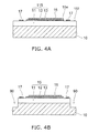
- the p-side electrode 16 is formed on the emitting region 15e, and the n-side electrode 17 is formed on the non-emitting region 15f.
- the p-side electrode 16 is in contact with the surface of the p-type semiconductor layer 12.
- the n-side electrode 17 is in contact with the surface of the n-type semiconductor layer 11, which is exposed by selectively removing the p-type semiconductor layer 12 and the light emitting layer 13.
- the p-side electrode 16 and the n-side electrode 17 are formed by using, for example, a sputtering method, an evaporation method, or the like. Either p-side electrode 16 or the n-side electrode 17 may be formed ahead of the other, or may be formed simultaneously using the same material.
- the p-side electrode 16 formed on the emitting area 15e includes a reflecting film which reflects the light emitted from the light emitting layer 13.
- the p-side electrode 16 includes, for example, silver, a silver alloy, aluminum, an aluminum alloy, or the like.
- the p-side electrode 16 may include a metal protective film (i.e. a barrier metal) for suppressing sulfuration or oxidation thereof.
- the n-type semiconductor layer 11 is selectively removed to form a trench 90.
- the semiconductor layer 115 is divided into a plurality of the semiconductor layers 15 by the trench 90.
- the trench 90 is etched into the semiconductor layer 115 and reaches the substrate 10.
- the substrate 10 is also etched to be recessed downward, so that a bottom of the trench 90 locates at a position lower than the interface between the substrate 10 and the semiconductor layer 15.
- the etching depth is set in the substrate 10 to be several micrometers or several tens micrometers, for example.
- the insulating film 18 is formed to cover a structure on the substrate 10, including the semiconductor layer 15.
- the insulating film 18 is, for example, a silicon oxide film or a silicon nitride film formed using a chemical vapor deposition (CVD) method.
- the insulating film 18 covers the second major surface 15b of the semiconductor layer 15, the p-side electrode 16, and the n-side electrode 17. In addition, the insulating film 18 covers the side surface 15c which is contiguous to the second major surface 15b of the semiconductor layer 15. The insulating film 18 covers the entire inner surface of the trench 90. The insulating film 18 is also formed on the surface of the substrate 10 which is exposed at the bottom of the trench 90.
- the openings 18a and the opening 18b are formed in the insulating film 18.
- the openings 18a communicate with the p-side electrode 16, and the opening 18b communicates with the n-side electrode 17.
- an underlying metal film 60 is formed, which covers the insulating film 18, the inner surface (the sidewalls and the bottom surface) of each opening 18a and the inner surface (the sidewalls and bottom surface) of the opening 18b.
- the underlying metal film 60 has a structure, wherein an aluminum film 61, a titanium film 62, and a copper film 63 are sequentially stacked on the insulating film 18.
- the underlying metal film 60 is formed, for example, using a sputtering method.
- the aluminum film 61 reflects the radiation light of the light emitting layer 13.
- the p-side interconnect layer 21, the n-side interconnect layer 22, and the metal film 50 are formed.
- the p-side interconnect layer 21, the n-side interconnect layer 22, and the metal film 50 are formed, for example, by selective copper plating using a resist mask 91 formed on the underlying metal film 60.
- the underlying metal film 60 serves as a seed layer, which conducts current, and the p-side interconnect layer 21, the n-side interconnect layer 22, and the metal film 50 are selectively formed on the copper film 63 of the underlying metal film 60.
- the p-side interconnect layer 21 is electrically connected to the p-side electrode 16 through the openings 18a.
- the n-side interconnect layer 22 is electrically connected to the n-side electrode 17 through the opening 18b.
- the resist mask 91 is removed, for example, using a solvent or oxygen plasma, and after that, as shown in FIG. 7A , a resist mask 92 is formed.
- a p-side metal pillar 23 and an n-side metal pillar 24 are formed on the p-side interconnect layer 21 and the n-side interconnect layer 22, respectively.
- the p-side metal pillar 23 and the n-side metal pillar 24 are formed, for example, by selective copper plating.
- the p-side metal pillar 23 is formed on the p-side interconnect layer 21.
- the p-side metal pillar 23 may join the p-side interconnect layer 21 to be one body, when being made of the same copper material.
- the n-side metal pillar 24 is formed on the n-side interconnect layer 22.
- the n-side metal pillar 24 may join the n-side interconnect layer 22 to be one body, when being made of the same copper material.
- the resist mask 92 covers the metal film 50. Therefore, either metal pillar is not provided on the metal film 50.
- the resist mask 92 is removed using a solvent or oxygen plasma, for example.
- the p-side interconnect layer 21 and the n-side interconnect layer 22 are electrically connected to each other through the underlying metal film 60.
- the p-side interconnect layer 21 and the metal film 50 are also electrically connected to each other through the underlying metal film 60
- the n-side interconnect layer 22 and the metal film 50 are also electrically connected to each other through the underlying metal film 60.
- the underlying metal film 60 are selectively removed by etching between the p-side interconnect layer 21 and the n-side interconnect layer 22, between the p-side interconnect layer 21 and the metal film 50, and between the n-side interconnect layer 22 and the metal film 50. Accordingly, the electrical connections are vanished between the p-side interconnect layer 21 and the n-side interconnect layer 22, between the p-side interconnect layer 21 and the metal film 50, and between the n-side interconnect layer 22 and the metal film 50.
- the p-side interconnect portion 41, the n-side interconnect portion 43, and the metal film 50 are formed on the side of the second major surface of the semiconductor layer 15.
- the p-side interconnect portion 41 includes the p-side interconnect layer 21 and the p-side metal pillar 23.
- the n-side interconnect portion 43 includes the n-side interconnect layer 22 and the n-side metal pillar 24.
- the metal film 50 formed around the side surface 15c of the semiconductor layer 15 is in an electrically floating state and does not act as an electrode.
- the metal film 50 includes the aluminum film 61 of the underlying metal film 60 and acts as a reflecting film.
- a plating film may not be formed on the side surface 15c of the semiconductor layer 15.
- the metal film 50 may be a portion of the underlying metal film 60 without the plating layer.
- the resist mask 91 is formed to cover the side surface 15c of the semiconductor layer 15, any plating film is not formed on the underlying metal film 60.
- the underlying metal film 60 is etched to leave a portion which is to be the metal film 50, when disconnecting the electrical connection between the p-side interconnect layer 21 and the n-side interconnect layer 22. In other words, if the portion which is to be the metal film 50 is covered with a resist film, the underlying metal film 60 remains on the insulating film 18, forming the metal film 50.
- the metal film 50 to be a thin film makes the dicing process of the semiconductor light emitting device 1 easier. In addition, it may be possible to suppress damages in the diced side surface, and to improve reliability of the semiconductor light emitting device 1.
- the resin layer 25 is formed to cover the p-side interconnect portion 41 and the n-side interconnect portion 43 and to embed the trench 90.
- the resin layer 25 covers the metal film 50 inside the trench 90.
- an epoxy resin, a silicon resin, a fluorine resin, or the like can be used for the resin layer 25.
- a black resin containing a light-shielding material such as carbon particles may be used for the resin layer 25. Accordingly, light leakage is reduced on the second major surface 15b side of the semiconductor layer 15.
- the resin layer 25 may contain a filler to adjust the flexibility thereof.
- the rear surface side of the substrate 10 is polished to reduce the thickness thereof.
- the polished thin substrate 10 is removed, for example, using wet etching.
- the substrate 10 may be removed, for example, using dry etching after the polishing.
- the resin layer 25, the p-side interconnect portion 41, and the n-side interconnect portion 43 support the semiconductor layer 15 to maintain the wafer shape, wherein a plurality of the semiconductor layers 15 are included.
- the semiconductor layer 15 which is may include a large internal stress, while being epitaxially grown on the substrate 10.
- the resin layer 25 may absorb the stress as a support body, which is more flexible than the semiconductor layer 15, and prevent the semiconductor layer 15 from destruction.
- the first major surface 15a of the semiconductor layer 15 and the insulating film 18 covering the resin layer 25 are exposed.
- fine roughness (not shown) may be preferably formed on the first major surface 15a.
- the side of the first major surface 15a of the semiconductor layer 15 is wet-etched using a KOH (potassium hydroxide) solution, TMAH (tetramethylammonium hydroxide), or the like. Due to difference in etching rate depending on orientation of a crystalline plane, the roughness can be formed on the first major surface 15a. The roughness in the first major surface 15a may improve extraction efficiency of the light emitted from the light emitting layer 13 to outward.
- KOH potassium hydroxide
- TMAH tetramethylammonium hydroxide
- the adhesive layer 73 is formed to cover the first major surface 15a of the semiconductor layer 15 and the insulating film 18.
- the adhesive layer 73 is, for example, an inorganic film such as a silicon nitride film or a silicon oxide film, and can be formed using a plasma CVD method.
- the adhesive layer 73 joins the insulating film 18 to be one film.
- a portion where the insulating film 18 and the adhesive layer 73 are stacked is described as the insulating film 18.
- the transparent layer 70 is formed on the adhesive layer 73 and the insulating film 18.
- the transparent layer 70 is thicker on the adhesive layer 73 (the semiconductor layer 15) than on the insulating film 18.
- a resin which transmits the light emitted from the light emitting layer 13 and the light radiated from the fluorescent substance 31 is used for the transparent layer 70.
- the portion of the transparent layer 70 is removed on the side opposite to the insulating film 18.
- the transparent layer 70 is polished to be thinner, leaving the portion thereof on the semiconductor layer 15 side.
- the final thickness of the transparent layer 70 is, for example, several micrometers or several tens micrometers.
- the side surface 70c of the transparent layer 70 remaining on the semiconductor layer 15 is covered with the metal film 50 via the insulating film 18.
- the adhesive layer 73 enhances the adhesion strength of the transparent layer 70.
- the fluorescent substance layer 30 is formed on the transparent layer 70 and the insulating film 18.
- the fluorescent substance layer 30 is also formed via the insulating film 18 on the resin layer 25 that surrounds the semiconductor layer 15 and the transparent layer 70.
- the fluorescent substance layer 30 is, for example, a resin layer including the fluorescent substance 31 and is formed using a method of printing, potting, molding, compression molding, or the like.
- a sintered body of fluorescent substance may be used for the fluorescent substance layer 30, wherein the fluorescent substances 31 are combined with the binder 33 other than the resin.
- the sintered body is bonded to the semiconductor layer 15 via the transparent layer 70.
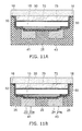
- the resin layer 25 is polished to, make the end face of the p-side metal pillar 23 and the end face of the n-side metal pillar 24 exposed.
- the end face of the p-side metal pillar 23 becomes a p-side external terminal 23a
- the end face of the n-side metal pillar 24 becomes an n-side external terminal 24a.
- the resin layer 25 is disposed between the p-side interconnect portion 41 and the n-side interconnect portion 43.
- the semiconductor light emitting devices 1 are diced by cutting the fluorescent substance layer 30, the insulating film 18, and the resin layer between the adjacent semiconductor layers 15.
- the fluorescent substance layer 30, the insulating film 18, and the resin layer 25 can be cut, for example, using a dicing blade or a laser beam. Since there is no part of the semiconductor layer 15 in the dicing area, it is possible to prevent the semiconductor layer 15 from the cutting damage.
- the semiconductor light emitting device 1 may have a single-chip structure including at least one semiconductor layer 15 or may have a multiple-chip structure including a plurality of the semiconductor layers 15.
- the diced semiconductor light emitting device 1 can be directly mounted on the circuit board, since the device is packaged together with the fluorescent substance layer 30. Accordingly, it is possible to reduce production cost.
- the semiconductor light emitting device 1 is a small-sized light source with a chip-size package that has high versatility.
- FIGS. 12A to 16 are schematic cross-sectional views illustrating semiconductor light emitting devices 2 to 9 according to the variation of the first embodiment.
- description of the portions including the same component as those of the semiconductor light emitting device 1 will be omitted, and different configurations will be described.
- the semiconductor light emitting device 2 shown in FIG. 12A includes a metal film 53 which covers the side surface 15c of the semiconductor layer 15 and the side surface 70c of the transparent layer 70.
- the metal film 53 includes, for example, a reflecting material such as aluminum.
- the side surface 70c of the transparent layer 70 is provided to be recessed toward the inner side from an outer edge 70b of the fluorescent substance layer 30.
- the metal film 53 i.e. the reflecting member covers an outer peripheral portion 30d between the outer edge 30b of the fluorescent substance layer 30 and the side surface 70c.
- the metal film 53 reflects light emitted from the light emitting layer 13 and propagating toward the side surface 15c of the semiconductor layer 15, and light emitted from the light emitting layer 13 and propagating through the transparent layer 70 toward the side surface 70c.
- the light emitted from the light emitting layer 13 and the light radiated from the fluorescent substance 31 are reflected toward the light emitting surface 30a. Accordingly, it is possible to improve the light output of the semiconductor light emitting device 2, and to suppress color unevenness and color breakup in the lateral direction (i.e. the direction parallel to the first major surface 15a).
- the metal film 53 is, for example, the underlying metal film 60 (refer to FIG. 6A ) and includes the aluminum film 61.
- the metal film 53 may also be formed using copper plating on the underlying metal film 60. As shown in FIG. 12A , it is preferable to use the underlying metal film 60 without copper plating for the metal film 53, since the semiconductor light emitting devices 2 are cut into dices so that the metal film 53 is exposed in an end face of each dice.
- the semiconductor light emitting device 3 shown in FIG. 12B includes a resin layer 27 instead of the resin layer 25.
- the resin layer 27 is, for example, a white resin including a reflecting material such as a titanium oxide, and reflects the light emitted from the light emitting layer 13 and the light radiated the fluorescent substance 31.
- the resin layer 27 fills the inside of the trench 90 surrounding the semiconductor layer 15, and covers the side surface 15c of the semiconductor layer 15 and the side surface 70c of the transparent layer 70 via the insulating film 18.
- the resin layer 27 reflects the light emitted from the light emitting layer 13, and propagates toward the side surface 15c of the semiconductor layer 15, and the light radiated from the light emitting layer 13, and propagates toward the side surface 70c.
- the resin layer 27 reflects the light emitted from the light emitting layer 13 and the light radiated from the fluorescent substance 31. Accordingly, it is possible to improve the light output power of the semiconductor light emitting device 2, and the color unevenness and color breakup in the lateral direction.
- the resin layer covering the p-side interconnect portion 41 and the n-side interconnect portion 43 may has, for example, a two-layered structure that includes the resin layer 27 formed to fill the inside of the trench 90 and the resin layer 25 formed on the resin layer 27.
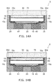
- the semiconductor light emitting device 4 shown in FIG. 13 includes a transparent layer 170 between the semiconductor layer 15 and the fluorescent substance layer 30.
- the transparent layer 170 is formed in a shape, wherein the central portion thereof is thin, and the thickness thereof increases as approaching the side surface 170c.
- the transparent layer 170 has a concave surface 170b on the fluorescent substance layer 30 side.
- the transparent layer 170 having such a shape can be formed, for example, by polishing the transparent layer 70 shown in FIG. 10A .
- the central portion thereof becomes thinner than the peripheral portion due to the so-called dishing effect.
- the light is scattered in the transparent layer 170. Accordingly, the distribution of the light radiated outward from the fluorescent substance layer 30 may be widened.
- the light propagating toward the side surface 15c of the semiconductor layer 15 and the light propagating toward the side surface 170c of the transparent layer 170 are reflected by the metal film 50.
- the light emitted from the light emitting layer 13 is suppressed in the lateral direction. Accordingly, in the light distribution characteristics of the semiconductor light emitting device 4, color unevenness, color breakup, and the like can be suppressed in the range of a large orientation angle.
- the outer peripheral portion 30d of the fluorescent substance layer 30 is in contact with the resin layer 25.
- the metal film 50 is in contact with the outer peripheral portion 30d of the fluorescent substance layer 30.
- This structure can be formed, for example, by removing the insulating film 18 formed on the resin layer 25 when the transparent layer 70 shown in FIG. 10A is polished to be a thinner transparent layer 70. In the polishing process of the transparent layer 70, the thickness thereof can be easily controlled. Thus, it becomes possible to improve the production efficiency of the semiconductor light emitting device 5.
- the side surface 70c of the transparent layer 70 is covered with the metal film 50 via the insulating film 18. Accordingly, the metal film 50 reflects the light emitted from the light emitting layer 13 and propagating through the transparent layer 70 in the lateral direction (the direction parallel to the first major surface 15a) toward the side surface 70c.
- an insulating film 75 is provided between the transparent layer 70 and the fluorescent substance layer 30.
- the insulating film 75 is, for example, an inorganic film such as a silicon oxide film or a silicon nitride film.
- the thickness of the insulating film 75 is, for example, substantially the same as those of the insulating films 18 and 73.
- the insulating film 75 is provided to extend to the outer edge of the fluorescent substance layer 30. Specifically, after the transparent layer 70 shown in FIG. 10A is thinned until the insulating film 18 is removed and the resin layer 25 is exposed, the insulating film 75 is formed to cover the transparent layer 70 and the resin layer 25.
- the insulating film 75 enhances, for example, the adhesion strength between the transparent layer 70 and the fluorescent substance layer 30.
- the insulating film 75 is interposed between the outer peripheral portion 30d of the fluorescent substance 30 and the resin layer 25 to enhance the adhesion strength therebetween.
- the insulating film 75 is effective in a case where the adhesion strength between the transparent layer 70 and the fluorescent substance layer 30 is low.
- by enhancing the adhesion strength between the outer peripheral portion 30d of the fluorescent substance layer 30 and the resin layer 25 infiltration of moistures or the like from the outside is suppressed, and thus, reliability can be improved in the semiconductor light emitting device 6.
- the resin layer 27 including a reflecting material may be used instead of the resin layer 25. Accordingly, the resin layer 27 reflects the light emitted from the light emitting layer 13 and propagating through the fluorescent substance layer 30, and the light radiated from the fluorescent substance 31 in the outer peripheral portion 30d.
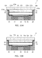
- the semiconductor light emitting device 7 shown in FIG. 15A includes a transparent layer 270 between the semiconductor layer 15 and the fluorescent substance layer 30.
- the transparent layer 270 has a third major surface 270a on the semiconductor layer 15 side and a fourth major surface 270b on a side opposite to the third major surface 270a.
- An outer edge 270d of the fourth major surface 270b is coincident with the outer edge 30b of the fluorescent substance layer 30.
- a side surface 270c which is in contact with the third major surface 270a is recessed toward the central side from the outer edge 270d.
- the side surface 270c is covered with the metal film 50 via the insulating film 18. Accordingly, the metal film may reflect the light emitted from the light emitting layer 13, and propagating through the transparent layer 270 in the lateral direction (the direction parallel to the first major surface 15a) toward the side surface 270c.
- a portion of the transparent layer 70 remains on the resin layer 25 after polishing the transparent layer 70 shown in FIG. 10A .
- the thickness can be easily controlled in the process of thinning the transparent layer 70.
- the side surface 15c of the semiconductor layer 15 and the side surface 70c of the transparent layer 70 are configured to be inclined.
- the semiconductor layer 15 is provided in a shape where the cross sectional area parallel to the first major surface 15a becomes larger as approaching the first major surface 15a.
- the transparent layer 70 is also provided in a similar shape where the cross sectional area parallel to the third major surface 70a becomes larger as approaching the fluorescent substance layer 30.
- the metal film 50 covering the side surface 15c and the side surface 70c is formed so that the inner surface is spread as extending opening in the direction toward the fluorescent substance layer 30.
- the metal film 50 may efficiently reflect the light propagating through the semiconductor layer 15 toward the side surface 15c and the light propagating through the transparent layer 70 toward the side surface 70c in the direction toward the fluorescent substance layer 30.
- the semiconductor light emitting device 10 the light radiated in the lateral direction is reduced to suppress the color unevenness and color breakup, and thus, the light output may be improved in the lateral direction.
- the metal film 50 is formed to cover an outer edge of the n-side electrode 17 (i.e. the edge on the side surface 15c side). In other words, the metal film 50 is provided to overlap the n-side electrode 17 on the second major surface 15b side.
- an overlap width ⁇ WL of the n-side electrode 17 and the metal film 50 is larger than zero in the entire outer edge of the n-side electrode 17.
- the p-side interconnect portion 41 and the n-side interconnect portion 43 are also provided to cover an inner edge of the n-side electrode 17 (i.e. the edge on the center side of the semiconductor layer 15). Accordingly, the light leakage can be suppressed on the second major surface 15b side. As a result, the light output power can be improved in the semiconductor light emitting device 9, and the resin layer 25 is prevented from degradation caused by the light irradiation, when the light emitting layer 13 emits light in the wavelength range of blue to ultraviolet.
- a semiconductor light emitting device 10 according to a second embodiment will be described with reference to FIGS. 17 to 20B .
- FIG. 17 is a schematic cross-sectional view illustrating the semiconductor light emitting device 10 according to the second embodiment.
- FIGS. 18A to 20B are schematic cross-sectional views illustrating processes of manufacturing the semiconductor light emitting device 10 according to the second embodiment.
- description of the portions including the same components as those of the semiconductor light emitting device 1 will be omitted, and a portion different therefrom will be described.
- the semiconductor light emitting device 10 includes a transparent layer 370 provided between the semiconductor layer 15 and the fluorescent substance layer 30.
- the transparent layer 370 has a third major surface 370a and a fourth major surface 370b at the side opposite to the third major surface 370a.
- the transparent layer 370 has a second side surface (hereinafter, referred to as a side surface 370c) which is in contact with the third major surface 370a and a third side surface (hereinafter, referred to as a side surface 370e) which is in contact with the fourth major surface 370b.
- the side surface 370e locates between the side surface 370c and the outer edge 30b of the fluorescent substance layer 30.
- the metal film 50 covers the side surface 15c of the semiconductor layer 15 and the side surface 370c. In addition, the metal film 50 may also cover the side surface 370e.
- the metal film 50 reflects the light emitted from the light emitting layer 13 and propagating through the semiconductor layer 15 toward the side surface 15c, and the light emitted from the light emitting layer 13 and propagating through the transparent layer 370 toward the side surface 370c. Accordingly, the light radiated in the lateral direction (the direction parallel to the first major surface 15a) is reduced, thus, improving the color unevenness and color breakup in the lateral direction.
- the metal film 50 is formed to cover the side surface 370e so that leakage of the radiation light of the light emitting layer 13 in the lateral direction can be further suppressed.
- FIG. 18A shows a resist mask 93 formed over the semiconductor layer 115.
- the resist mask 93 covers the emitting area 15e, the p-side electrode 16, the n-side electrode 17, and a portion of the non-emitting area 15f.
- the trench 90 is formed by selectively removing the semiconductor layer 115 using the resist mask 93.
- the semiconductor layer 115 is divided into a plurality of the semiconductor layers 15 by the trench 90.
- the trench 90 is formed to reach the substrate 10.
- the substrate 10 is also etched to be recessed downward so that a bottom of the trench 90 locates at a level lower than the interface between the substrate 10 and the semiconductor layer 15.
- the etching depth of the substrate 10 is set to be, for example, several micrometers or several tens micrometers.
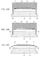
- the resist mask 93 is removed after forming the trench 90, as shown in FIG. 18C .
- a resist mask 94 is formed as shown in FIG. 19A , which covers the semiconductor layer 15, the p-side electrode 16, the n-side electrode 17, and a portion of the trench 90.
- FIG. 19B further etching using the resist mask 94 is performed to form a trench 95 in the substrate 10.
- the trench 95 is formed by selectively digging the bottom of the trench 90.
- the resist mask 94 is removed as shown in FIG. 19C after forming the trench 95.
- the insulating film 18 is formed, which covers the inner surfaces of the trenches 90 and 95 provided in the substrate 10 and the structure including the semiconductor layer 15 provided on the substrate 10.
- the insulating film 18, for example, is a silicon oxide film or a silicon nitride film formed using a chemical vapor deposition (CVD) method.
- the openings 18a and the opening 18b are formed in the insulating film 18.
- the openings 18a communicate with the p-side electrode 16, and the opening 18b communicates with the n-side electrode 17.
- the semiconductor light emitting device 10 may be completed through the manufacturing processes shown in FIGS. 5B to 11B .
- the structures of the semiconductor light emitting devices shown in FIG. 1 , FIG. 12A to FIG. 16 , and FIG. 17 are not limited to the above-described embodiments.
- the semiconductor light emitting device may have a structure combining the configurations thereof.
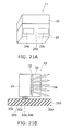
- FIGS. 21A and 21B are schematic cross-sectional views illustrating a semiconductor light emitting device 11 according to a third embodiment.
- the semiconductor light emitting device 11 has a side-view type structure in which external terminals 23b and 24b are provided on the side surface of the resin layer 25.
- the external terminals 23b and 24b electrically connect the semiconductor light emitting device 11 to the circuit board, for example.
- the metal pillars 23 and 24 are exposed in a different face of the resin layer 25 from the first and second embodiments.
- Other configurations are the same as those of the semiconductor light emitting devices 1 to 8.
- FIG. 21A is a schematic perspective view showing the semiconductor light emitting device 11.
- FIG. 21B is a schematic cross-sectional view of a light emitting module, wherein the semiconductor light emitting device 11 is mounted on a mounting substrate 310.
- An end face of the p-side metal pillar 23 is exposed in a fifth surface 25b of the resin layer 25.
- the fifth surface 25b is different in the surface orientation from the first major surface 15a of the semiconductor layer 15 and the second major surface 15b at the opposite side thereof.
- the end face of the p-side metal pillar 23 acts as the p-side external terminal 23b for electrically connecting the device to the mounting substrate 310.
- the fifth surface 25b is substantially perpendicular to the first major surface 15a and the second major surface 15b of the semiconductor layer 15.
- the resin layer 25 has, for example, four side surfaces, and one of the side surfaces is the fifth surface 25b.
- An end face of the n-side metal pillar 24 is exposed in the fifth surface 25b.
- the end face of the n-side metal pillar 24 acts as the n-side external terminal 24b for electrically connecting the device to the mounting substrate 310.
- the portion other than the p-side external terminal 23b exposed to the fifth surface 25b is covered with the resin layer 25.
- the portion other than the n-side external terminal 24b exposed to the fifth surface 25b is covered with the resin layer 25.
- the semiconductor light emitting device 11 is mounted on the mounting substrate 310 so that the fifth surface 25b faces a mounting surface 301.
- the p-side external terminal 23b and the n-side external terminal 24b which are exposed to the fifth surface 25b are attached to pads 302 provided on the mounting surface 301 using solder 303.
- a interconnect pattern which is connected to, for example, an external circuit is provided on the mounting surface 301, and the pad 302 is connected to the interconnect pattern.
- the fifth surface 25b is substantially perpendicular to the first major surface 15a which is a light emitting surface. Since the fifth surface 25b faces the mounting surface 301, the first major surface 15a is directed in the lateral direction parallel to the mounting surface 301 or in the inclined direction with respect to the mounting surface 301. In other words, the semiconductor light emitting device 11 emits light in the lateral direction parallel to the mounting surface 301 or in the inclined direction with respect to the mounting surface 301.
Landscapes
- Led Device Packages (AREA)
Abstract
Description
- Embodiments are related generally to a semiconductor light emitting device.
- Semiconductor light emitting devices having a chip-size package structure have been developed, using a light emitting diode (LED) combined with a fluorescent substance. The semiconductor light emitting devices can radiate visible light such as white light or light in other wavelength band, and be used for various applications. In such devices, however, there is a room for improvement in light characteristics, for example, light output power or emission color.
-
-
FIG. 1 is a schematic cross-sectional view showing an example of a semiconductor light emitting device according to a first embodiment; -
FIGS. 2A and 2B are schematic plan views showing an example of the semiconductor light emitting device according to the first embodiment; -
FIGS. 3A to 11B are schematic cross-sectional views showing an example of a manufacturing process of the semiconductor light emitting device according to the first embodiment; -
FIGS. 12A to 16 are schematic cross-sectional views showing examples of a semiconductor light emitting device according to a variation of the first embodiment; -
FIG. 17 is a schematic cross-sectional view showing an example of a semiconductor light emitting device according to a second embodiment; -
FIGS. 18A to 20B are schematic cross-sectional views showing an example of a manufacturing process of the semiconductor light emitting device according to the second embodiment; and -
FIGS. 21A and 21B are schematic cross-sectional views showing an example of a semiconductor light emitting device according to a third embodiment. - According to an embodiment, a semiconductor light emitting device includes a semiconductor layer, a p-side interconnect portion, an n-side interconnect portion, a fluorescent substance layer and a transparent layer. The semiconductor layer has a first major surface, a second major surface on a side opposite to the first major surface, and a first side surface being in contact with the first major surface and the second major surface, the semiconductor layer including a light emitting layer. The p-side interconnect portion is electrically connected to the semiconductor layer on the second major surface side, and the n-side interconnect portion is electrically connected to the semiconductor layer on the second major surface side. The fluorescent substance layer is provided on the first major surface side, and includes a fluorescent substance radiating light different in a wavelength from light emitted from the light emitting layer. The transparent layer is provided between the semiconductor layer and the fluorescent substance layer, and has a third major surface on the semiconductor layer side, a fourth major surface on the fluorescent substance layer side, and a second side surface being in contact with the third major surface, the transparent layer transmitting the light emitted from the light emitting layer.
- The device further includes an insulating film covering the first side surface and the second side surface, and a reflecting member covering the first side surface and the second side surface via the insulating film.
- Hereinafter, embodiments of the invention will be described with reference to the drawings. In the drawings, the same portions are denoted by the same reference numerals, detailed description thereof is appropriately omitted, and portions different therefrom are described. Incidentally, the drawings are illustrated schematically or conceptually, and a relation between thickness and width of each portion, a ratio of sizes between the portions, and the like may not be necessarily the same as those of the actual cases. In addition, even in a case where the same portion is shown, the dimension or ratio thereof may be different according to the drawings.
-
FIG. 1 is a schematic cross-sectional view illustrating a semiconductor light emitting device 1 according to a first embodiment. -
FIGS. 2A and 2B are schematic plan views illustrating the semiconductor light emitting device 1 according to the first embodiment. - The semiconductor light emitting device 1 includes a
semiconductor layer 15, a p-side interconnect portion 41, an n-side interconnect portion 43 and afluorescent substance layer 30. The p-side interconnect portion 41 and the n-side interconnect portion 43 are electrically connected to thesemiconductor layer 15. - The
semiconductor layer 15 has a firstmajor surface 15a, a secondmajor surface 15b (refer toFIG. 3A ) at the opposite side of the firstmajor surface 15a, and a first side surface (hereinafter, referred to as aside surface 15c). The first side surface is in contact with the firstmajor surface 15a and the secondmajor surface 15b. Thesemiconductor layer 15 includes an n-type semiconductor layer 11, a p-type semiconductor layer 12, and alight emitting layer 13. Thelight emitting layer 13 is provided between the n-type semiconductor layer 11 and the p-type semiconductor layer 12. - The p-
side interconnect portion 41 and the n-side interconnect portion 43 are electrically connected to thesemiconductor layer 15 on the side of the secondmajor surface 15b. The p-side interconnect portion 41 is electrically connected to a p-side electrode 16 which is in contact with the p-type semiconductor layer 12. The n-side interconnect portion 43 is electrically connected to an n-side electrode 17 which is in contact with the n-type semiconductor layer 11. - A
resin layer 25 is provided between the p-side interconnect portion 41 and the n-side interconnect portion 43. The p-side interconnect portion 41, the n-side interconnect portion 43, and theresin layer 25 constitute a support body which supports thesemiconductor layer 15. - The
fluorescent substance layer 30 is provided on the side of the firstmajor surface 15a of thesemiconductor layer 15. Thefluorescent substance layer 30 includes afluorescent substance 31. Thefluorescent substance 31 is excited by the radiation light of the light emitting layer and radiates light having a wavelength different from that of the radiation light. - In the embodiment, a
transparent layer 70 is provided between thesemiconductor layer 15 and thefluorescent substance layer 30. The radiation light of thelight emitting layer 13 propagates through the transparent layer. Herein, the term "transparent" is not limited to the case where 100% of the radiation light propagates through thetransparent layer 70, but it may also include a case where a portion of the radiation light is absorbed. - The
transparent layer 70 has a thirdmajor surface 70a on the side of thesemiconductor layer 15. The thirdmajor surface 70a is provided to be parallel to the firstmajor surface 15a. Thetransparent layer 70 has a second side surface (hereinafter, referred to as aside surface 70c) which is in contact with the thirdmajor surface 70a. - The semiconductor light emitting device 1 includes an
insulating film 18 and ametal film 50. Theinsulating film 18 covers theside surface 15c and theside surface 70c, and themetal film 50 covers theside surface 15c and theside surface 70c via theinsulating film 18. Themetal film 50 includes a reflecting member which reflects the radiation light of thelight emitting layer 13. In the description hereinafter, the term "cover" means not only a case where "something to cover" is in direct contact with "something to be covered", but also a case where "something to cover" is provided on "something to be covered" with another element being interposed. -
FIG. 2A is a schematic plan view showing the secondmajor surface 15b of thesemiconductor layer 15, wherein the p-side interconnect portion 41, the n-side interconnect portion 43, theresin layer 25, and theinsulating film 18 are removed for exposing the secondmajor surface 15b. - The second
major surface 15b of thesemiconductor layer 15 has a portion including the light emitting layer 13 (herein after emittingregion 15e), and a portion including no light emitting layer 13 (herein after non-emittingregion 15f). The p-side electrode 16 is formed on the emittingregion 15e. The n-side electrode 17 is formed on thenon-emitting region 15f. - As shown in
FIG. 2A , thenon-emitting region 15f is provided to surround, for example, the emittingregion 15e. In addition, the n-side electrode 17 may be provided to surround, for example, the p-side electrode 16.FIGS. 2A and 2B illustrate an example of planar arrangement of the p-side electrode 16 and the n-side electrode 17, but the embodiment is not limited thereto. -
FIG. 2B is a schematic plan view showing a p-side interconnect layer 21, an n-side interconnect layer 22, and themetal film 50 which are provided on the side of the secondmajor surface 15b of thesemiconductor layer 15. - The p-
side interconnect layer 21, the n-side interconnect layer 22, and themetal film 50 are provided on the insulatingfilm 18 which covers thesemiconductor layer 15, the p-side electrode 16, and the n-side electrode 17. The p-side interconnect layer 21 is electrically connected to the p-side electrode 16 throughopenings 18a provided in the insulatingfilm 18. - The area of the
emitting region 15e is provided to be larger than the area of thenon-emitting region 15f so that light output power is improved. A plurality of theopenings 18a communicating with the p-side electrode 16 are provided in the insulatingfilm 18 so that the current may uniformly flows into theemitting region 15e. The embodiment is not limited to the example. For example, the p-side interconnect layer 21 may be connected to the p-side electrode 16 through one opening which has a larger area than that of theopening 18a shown inFIG. 2B . - The n-
side interconnect layer 22 is electrically connected to the n-side electrode 17 throughopening 18b provided in the insulatingfilm 18. - For example, the p-
side electrode 16, the n-side electrode 17, the p-side interconnect layer 21, the n-side interconnect layer 22, and themetal film 50 may preferably include a member which reflects the radiation light of thelight emitting layer 13, since they are provided on the side of the secondmajor surface 15b of thesemiconductor layer 15. - In the semiconductor light emitting device 1, the
light emitting layer 13 emits light generated by supplying current to thelight emitting layer 13 through the p-side electrode 16 and the n-side electrode 17. The light radiated from thelight emitting layer 13 is extracted from the side of the firstmajor surface 15a to the outside of thesemiconductor layer 15. Thus, if the p-side electrode 16, the n-side electrode 17, the p-side interconnect layer 21, the n-side interconnect layer 22, and themetal film 50, which are provided at the side of the secondmajor surface 15b, can preferably act as a reflecting layer, improving the intensity of the light emitted from the side of the firstmajor surface 15a of thesemiconductor layer 15. - The
fluorescent substance layer 30 is provided on the firstmajor surface 15a of thesemiconductor layer 15. Thefluorescent substance layer 30 includes thefluorescent substance 31. Thefluorescent substance 31 absorbs part of the light emitted from thelight emitting layer 13 and radiates light having a wavelength different from that of the light emitted from thelight emitting layer 13. In other words, thefluorescent substance 31 has an emission spectrum different from the emission spectrum of thelight emitting layer 13. Thefluorescent substance 31 is combined with abinder 33. Thebinder 33 is, for example, a resin which transmits the light emitted from thelight emitting layer 13 and the light radiated from thefluorescent substance 31. - The semiconductor light emitting device 1 emits light from a
light emitting surface 30a of thefluorescent substance layer 30, which includes the light emitted from thelight emitting layer 13 and the light radiated from thefluorescent substance 31. Moreover, it is possible to change emission color by adjusting a type and content of thefluorescent substance 31. Thefluorescent substance 31 is not limited to one type of a fluorescent substance, but thefluorescent substance layer 30 may include plural types of fluorescent substances. - The
transparent layer 70 is provided between thesemiconductor layer 15 and thefluorescent substance layer 30. The light extracted from thesemiconductor layer 15 propagates through thetransparent layer 70, and enters thefluorescent substance layer 30. Thetransparent layer 70 is preferably formed to have high transmittance against the light that is directed from thesemiconductor layer 15 toward thefluorescent substance layer 30, and high reflectance against the light that is directed from thefluorescent substance layer 30 toward thesemiconductor layer 15. - For example, when the refractive index of the
transparent layer 70 is set to be smaller than the refractive index of thefluorescent substance layer 30, the light radiated from thefluorescent substance 31 may be reflected at the interface between thefluorescent substance layer 30 and thetransparent layer 70. In addition, the light may be suppressed, which is reflected at thelight emitting surface 30a of thefluorescent substance layer 30, and returns to thesemiconductor layer 15. Thus, the light output power of the semiconductor light emitting device 1 may increase by reducing light absorption in thesemiconductor layer 15. - A transparent resin can be used for the
transparent layer 70. For example, it may be possible for thetransparent layer 70 to use the same resin as thebinder 33 of thefluorescent substance layer 30. The refractive index of thefluorescent substance layer 30 including thefluorescent substance 31 becomes higher than the refractive index of thetransparent layer 70 not including the fluorescent substance. According, the light directed from thefluorescent substance layer 30 toward thesemiconductor layer 15 is reflected at the interface between thefluorescent substance layer 30 and thetransparent layer 70, and the light output power may be improved in the semiconductor light emitting device 1. - In a case where a resin is used for the
transparent layer 70, it is desirable to provide anadhesive layer 73 between thesemiconductor layer 15 and thetransparent layer 70. For example, an inorganic film such as a silicon oxide film or a silicon nitride film may be used for theadhesive layer 73. - In the embodiment, the
metal film 50 covers theside surface 70c of thetransparent layer 70. Themetal film 50 reflects the light propagating in the lateral direction (the direction parallel to the firstmajor surface 15a) among the lights radiated from thelight emitting layer 13. Thus, the light radiated from the side surface is reduced in the semiconductor light emitting device 1, and the variation of emission color, so-called color breakup or color unevenness is suppressed in the lateral direction. - Next, a method of manufacturing the semiconductor light emitting device 1 will be described with reference to
FIGS. 3A to 11B . -
FIG. 3A is a cross-sectional view showing asemiconductor layer 115 formed on asubstrate 10. The n-type semiconductor layer 11, thelight emitting layer 13, and the p-type semiconductor layer 12 are epitaxially grown in this order on thesubstrate 10, for example, using a metal organic chemical vapor deposition (MOCVD) method. A surface on thesubstrate 10 side of thesemiconductor layer 15 is the firstmajor surface 15a, and a surface opposite to the firstmajor surface 15a is the secondmajor surface 15b. - The
substrate 10 is, for example, a silicon substrate. Thesemiconductor layer 115 is, for example, a nitride semiconductor layer, and includes gallium nitride (GaN) or the like. - The n-
type semiconductor layer 11 may include, for example, a buffer layer provided on the major surface of thesubstrate 10 and an n-type GaN layer provided on the buffer layer. The p-type semiconductor layer 12 may include, for example, a p-type AlGaN layer provided on thelight emitting layer 13 and a p-type GaN layer provided on the p-type AlGaN layer. Thelight emitting layer 13 has, for example, a multiple quantum well (MQW) structure. Thelight emitting layer 13 may include a material which emits light such as blue, violet, blue violet or ultraviolet light. In the emission spectrum of thelight emitting layer 13, the peak wavelength is, for example, in a range of 430 nm to 470 nm. - In
FIG. 3B , the p-type semiconductor layer 12 and thelight emitting layer 13 are selectively removed, and a portion of the n-type semiconductor layer 11 is exposed. For example, the p-type semiconductor layer 12 and thelight emitting layer 13 are selectively etched by using a reactive ion etching (RIE) method, thus exposing the portion of the n-type semiconductor layer 11. Thereby, the emittingregion 15e including thelight emitting layer 13 and thenon-emitting region 15f not including thelight emitting layer 13 are formed on the secondmajor surface 15b side. - As shown in
FIG. 4A , the p-side electrode 16 is formed on theemitting region 15e, and the n-side electrode 17 is formed on thenon-emitting region 15f. The p-side electrode 16 is in contact with the surface of the p-type semiconductor layer 12. The n-side electrode 17 is in contact with the surface of the n-type semiconductor layer 11, which is exposed by selectively removing the p-type semiconductor layer 12 and thelight emitting layer 13. - The p-
side electrode 16 and the n-side electrode 17 are formed by using, for example, a sputtering method, an evaporation method, or the like. Either p-side electrode 16 or the n-side electrode 17 may be formed ahead of the other, or may be formed simultaneously using the same material. - The p-
side electrode 16 formed on the emittingarea 15e includes a reflecting film which reflects the light emitted from thelight emitting layer 13. The p-side electrode 16 includes, for example, silver, a silver alloy, aluminum, an aluminum alloy, or the like. In addition, the p-side electrode 16 may include a metal protective film (i.e. a barrier metal) for suppressing sulfuration or oxidation thereof. - As shown in
FIG. 4B , the n-type semiconductor layer 11 is selectively removed to form atrench 90. Thesemiconductor layer 115 is divided into a plurality of the semiconductor layers 15 by thetrench 90. Thetrench 90 is etched into thesemiconductor layer 115 and reaches thesubstrate 10. In the embodiment, thesubstrate 10 is also etched to be recessed downward, so that a bottom of thetrench 90 locates at a position lower than the interface between thesubstrate 10 and thesemiconductor layer 15. The etching depth is set in thesubstrate 10 to be several micrometers or several tens micrometers, for example. - Next, as shown in
FIG. 5A , the insulatingfilm 18 is formed to cover a structure on thesubstrate 10, including thesemiconductor layer 15. The insulatingfilm 18 is, for example, a silicon oxide film or a silicon nitride film formed using a chemical vapor deposition (CVD) method. - The insulating
film 18 covers the secondmajor surface 15b of thesemiconductor layer 15, the p-side electrode 16, and the n-side electrode 17. In addition, the insulatingfilm 18 covers theside surface 15c which is contiguous to the secondmajor surface 15b of thesemiconductor layer 15. The insulatingfilm 18 covers the entire inner surface of thetrench 90. The insulatingfilm 18 is also formed on the surface of thesubstrate 10 which is exposed at the bottom of thetrench 90. - Subsequently, the
openings 18a and theopening 18b are formed in the insulatingfilm 18. Theopenings 18a communicate with the p-side electrode 16, and theopening 18b communicates with the n-side electrode 17. - Next, as shown in
FIG. 5B , anunderlying metal film 60 is formed, which covers the insulatingfilm 18, the inner surface (the sidewalls and the bottom surface) of eachopening 18a and the inner surface (the sidewalls and bottom surface) of theopening 18b. - As shown in
FIG. 6A , theunderlying metal film 60 has a structure, wherein analuminum film 61, atitanium film 62, and acopper film 63 are sequentially stacked on the insulatingfilm 18. Theunderlying metal film 60 is formed, for example, using a sputtering method. Thealuminum film 61 reflects the radiation light of thelight emitting layer 13. - Next, as shown in
FIG. 6B , the p-side interconnect layer 21, the n-side interconnect layer 22, and themetal film 50 are formed. The p-side interconnect layer 21, the n-side interconnect layer 22, and themetal film 50 are formed, for example, by selective copper plating using a resistmask 91 formed on theunderlying metal film 60. Theunderlying metal film 60 serves as a seed layer, which conducts current, and the p-side interconnect layer 21, the n-side interconnect layer 22, and themetal film 50 are selectively formed on thecopper film 63 of theunderlying metal film 60. The p-side interconnect layer 21 is electrically connected to the p-side electrode 16 through theopenings 18a. The n-side interconnect layer 22 is electrically connected to the n-side electrode 17 through theopening 18b. - Next, the resist
mask 91 is removed, for example, using a solvent or oxygen plasma, and after that, as shown inFIG. 7A , a resistmask 92 is formed. In addition, a p-side metal pillar 23 and an n-side metal pillar 24 are formed on the p-side interconnect layer 21 and the n-side interconnect layer 22, respectively. - The p-
side metal pillar 23 and the n-side metal pillar 24 are formed, for example, by selective copper plating. The p-side metal pillar 23 is formed on the p-side interconnect layer 21. The p-side metal pillar 23 may join the p-side interconnect layer 21 to be one body, when being made of the same copper material. The n-side metal pillar 24 is formed on the n-side interconnect layer 22. The n-side metal pillar 24 may join the n-side interconnect layer 22 to be one body, when being made of the same copper material. The resistmask 92 covers themetal film 50. Therefore, either metal pillar is not provided on themetal film 50. - Subsequently, the resist
mask 92 is removed using a solvent or oxygen plasma, for example. At this time, the p-side interconnect layer 21 and the n-side interconnect layer 22 are electrically connected to each other through theunderlying metal film 60. In addition, the p-side interconnect layer 21 and themetal film 50 are also electrically connected to each other through theunderlying metal film 60, and the n-side interconnect layer 22 and themetal film 50 are also electrically connected to each other through theunderlying metal film 60. - In the following process, the
underlying metal film 60 are selectively removed by etching between the p-side interconnect layer 21 and the n-side interconnect layer 22, between the p-side interconnect layer 21 and themetal film 50, and between the n-side interconnect layer 22 and themetal film 50. Accordingly, the electrical connections are vanished between the p-side interconnect layer 21 and the n-side interconnect layer 22, between the p-side interconnect layer 21 and themetal film 50, and between the n-side interconnect layer 22 and themetal film 50. - As shown in
FIG. 7B , the p-side interconnect portion 41, the n-side interconnect portion 43, and themetal film 50 are formed on the side of the second major surface of thesemiconductor layer 15. The p-side interconnect portion 41 includes the p-side interconnect layer 21 and the p-side metal pillar 23. The n-side interconnect portion 43 includes the n-side interconnect layer 22 and the n-side metal pillar 24. - The
metal film 50 formed around theside surface 15c of thesemiconductor layer 15 is in an electrically floating state and does not act as an electrode. Themetal film 50 includes thealuminum film 61 of theunderlying metal film 60 and acts as a reflecting film. - In addition, in the process shown in
FIG. 5B , a plating film may not be formed on theside surface 15c of thesemiconductor layer 15. In other words, themetal film 50 may be a portion of theunderlying metal film 60 without the plating layer. For example, if the resistmask 91 is formed to cover theside surface 15c of thesemiconductor layer 15, any plating film is not formed on theunderlying metal film 60. - In the case of using the
underlying metal film 60 as themetal film 50, theunderlying metal film 60 is etched to leave a portion which is to be themetal film 50, when disconnecting the electrical connection between the p-side interconnect layer 21 and the n-side interconnect layer 22. In other words, if the portion which is to be themetal film 50 is covered with a resist film, theunderlying metal film 60 remains on the insulatingfilm 18, forming themetal film 50. - In this manner, forming the
metal film 50 to be a thin film makes the dicing process of the semiconductor light emitting device 1 easier. In addition, it may be possible to suppress damages in the diced side surface, and to improve reliability of the semiconductor light emitting device 1. - Next, as shown in
FIG. 8A , theresin layer 25 is formed to cover the p-side interconnect portion 41 and the n-side interconnect portion 43 and to embed thetrench 90. Theresin layer 25 covers themetal film 50 inside thetrench 90. For example, an epoxy resin, a silicon resin, a fluorine resin, or the like can be used for theresin layer 25. For example, a black resin containing a light-shielding material such as carbon particles may be used for theresin layer 25. Accordingly, light leakage is reduced on the secondmajor surface 15b side of thesemiconductor layer 15. In addition, theresin layer 25 may contain a filler to adjust the flexibility thereof. - Subsequently, as shown in
FIG. 8B , the rear surface side of thesubstrate 10 is polished to reduce the thickness thereof. As shown inFIG. 9A , the polishedthin substrate 10 is removed, for example, using wet etching. Alternatively, thesubstrate 10 may be removed, for example, using dry etching after the polishing. - After removing the
substrate 10, theresin layer 25, the p-side interconnect portion 41, and the n-side interconnect portion 43 support thesemiconductor layer 15 to maintain the wafer shape, wherein a plurality of the semiconductor layers 15 are included. - For example, in some cases, the
semiconductor layer 15 which is may include a large internal stress, while being epitaxially grown on thesubstrate 10. When the internal stress during the epitaxial growth is released at the time of removing thesubstrate 10, theresin layer 25 may absorb the stress as a support body, which is more flexible than thesemiconductor layer 15, and prevent thesemiconductor layer 15 from destruction. - After removing the
substrate 10, the firstmajor surface 15a of thesemiconductor layer 15 and the insulatingfilm 18 covering theresin layer 25 are exposed. In addition, fine roughness (not shown) may be preferably formed on the firstmajor surface 15a. - For example, the side of the first
major surface 15a of thesemiconductor layer 15 is wet-etched using a KOH (potassium hydroxide) solution, TMAH (tetramethylammonium hydroxide), or the like. Due to difference in etching rate depending on orientation of a crystalline plane, the roughness can be formed on the firstmajor surface 15a. The roughness in the firstmajor surface 15a may improve extraction efficiency of the light emitted from thelight emitting layer 13 to outward. - Next, as shown in
FIG. 9B , theadhesive layer 73 is formed to cover the firstmajor surface 15a of thesemiconductor layer 15 and the insulatingfilm 18. Theadhesive layer 73 is, for example, an inorganic film such as a silicon nitride film or a silicon oxide film, and can be formed using a plasma CVD method. - For example, in a case where the insulating
film 18 and theadhesive layer 73 are films formed by using the same material, theadhesive layer 73 joins the insulatingfilm 18 to be one film. In the description hereinafter, a portion where the insulatingfilm 18 and theadhesive layer 73 are stacked is described as the insulatingfilm 18. - Next, as shown in
FIG. 10A , thetransparent layer 70 is formed on theadhesive layer 73 and the insulatingfilm 18. Thetransparent layer 70 is thicker on the adhesive layer 73 (the semiconductor layer 15) than on the insulatingfilm 18. For example, a resin which transmits the light emitted from thelight emitting layer 13 and the light radiated from thefluorescent substance 31 is used for thetransparent layer 70. - Next, as shown in
FIG. 10B , the portion of thetransparent layer 70 is removed on the side opposite to the insulatingfilm 18. For example, thetransparent layer 70 is polished to be thinner, leaving the portion thereof on thesemiconductor layer 15 side. The final thickness of thetransparent layer 70 is, for example, several micrometers or several tens micrometers. Theside surface 70c of thetransparent layer 70 remaining on thesemiconductor layer 15 is covered with themetal film 50 via the insulatingfilm 18. Theadhesive layer 73 enhances the adhesion strength of thetransparent layer 70. - Next, as shown in
FIG. 11A , thefluorescent substance layer 30 is formed on thetransparent layer 70 and the insulatingfilm 18. Thefluorescent substance layer 30 is also formed via the insulatingfilm 18 on theresin layer 25 that surrounds thesemiconductor layer 15 and thetransparent layer 70. Thefluorescent substance layer 30 is, for example, a resin layer including thefluorescent substance 31 and is formed using a method of printing, potting, molding, compression molding, or the like. - In addition, a sintered body of fluorescent substance may be used for the
fluorescent substance layer 30, wherein thefluorescent substances 31 are combined with thebinder 33 other than the resin. The sintered body is bonded to thesemiconductor layer 15 via thetransparent layer 70. - Next, as shown in
FIG. 11B , theresin layer 25 is polished to, make the end face of the p-side metal pillar 23 and the end face of the n-side metal pillar 24 exposed. The end face of the p-side metal pillar 23 becomes a p-sideexternal terminal 23a, and the end face of the n-side metal pillar 24 becomes an n-sideexternal terminal 24a. Thus, theresin layer 25 is disposed between the p-side interconnect portion 41 and the n-side interconnect portion 43. - Subsequently, the semiconductor light emitting devices 1 are diced by cutting the
fluorescent substance layer 30, the insulatingfilm 18, and the resin layer between the adjacent semiconductor layers 15. Thefluorescent substance layer 30, the insulatingfilm 18, and theresin layer 25 can be cut, for example, using a dicing blade or a laser beam. Since there is no part of thesemiconductor layer 15 in the dicing area, it is possible to prevent thesemiconductor layer 15 from the cutting damage. - The semiconductor light emitting device 1 may have a single-chip structure including at least one
semiconductor layer 15 or may have a multiple-chip structure including a plurality of the semiconductor layers 15. The diced semiconductor light emitting device 1 can be directly mounted on the circuit board, since the device is packaged together with thefluorescent substance layer 30. Accordingly, it is possible to reduce production cost. The semiconductor light emitting device 1 is a small-sized light source with a chip-size package that has high versatility. - Next, semiconductor light emitting devices according to variation of the first embodiment will be described with reference to
FIGS. 12A to 16 . -
FIGS. 12A to 16 are schematic cross-sectional views illustrating semiconductorlight emitting devices 2 to 9 according to the variation of the first embodiment. Hereinafter, description of the portions including the same component as those of the semiconductor light emitting device 1 will be omitted, and different configurations will be described. - The semiconductor
light emitting device 2 shown inFIG. 12A includes ametal film 53 which covers theside surface 15c of thesemiconductor layer 15 and theside surface 70c of thetransparent layer 70. Themetal film 53 includes, for example, a reflecting material such as aluminum. - As shown in
FIG. 12A , theside surface 70c of thetransparent layer 70 is provided to be recessed toward the inner side from anouter edge 70b of thefluorescent substance layer 30. On thetransparent layer 70 side of thefluorescent substance layer 30, the metal film 53 (i.e. the reflecting member) covers an outerperipheral portion 30d between theouter edge 30b of thefluorescent substance layer 30 and theside surface 70c. - The
metal film 53 reflects light emitted from thelight emitting layer 13 and propagating toward theside surface 15c of thesemiconductor layer 15, and light emitted from thelight emitting layer 13 and propagating through thetransparent layer 70 toward theside surface 70c. In the outerperipheral portion 30d of thefluorescent substance layer 30, the light emitted from thelight emitting layer 13 and the light radiated from thefluorescent substance 31 are reflected toward thelight emitting surface 30a. Accordingly, it is possible to improve the light output of the semiconductorlight emitting device 2, and to suppress color unevenness and color breakup in the lateral direction (i.e. the direction parallel to the firstmajor surface 15a). - The
metal film 53 is, for example, the underlying metal film 60 (refer toFIG. 6A ) and includes thealuminum film 61. Themetal film 53 may also be formed using copper plating on theunderlying metal film 60. As shown inFIG. 12A , it is preferable to use theunderlying metal film 60 without copper plating for themetal film 53, since the semiconductorlight emitting devices 2 are cut into dices so that themetal film 53 is exposed in an end face of each dice. - The semiconductor
light emitting device 3 shown inFIG. 12B includes aresin layer 27 instead of theresin layer 25. Theresin layer 27 is, for example, a white resin including a reflecting material such as a titanium oxide, and reflects the light emitted from thelight emitting layer 13 and the light radiated thefluorescent substance 31. - The
resin layer 27 fills the inside of thetrench 90 surrounding thesemiconductor layer 15, and covers theside surface 15c of thesemiconductor layer 15 and theside surface 70c of thetransparent layer 70 via the insulatingfilm 18. Theresin layer 27 reflects the light emitted from thelight emitting layer 13, and propagates toward theside surface 15c of thesemiconductor layer 15, and the light radiated from thelight emitting layer 13, and propagates toward theside surface 70c. In addition, in the outerperipheral portion 30d of thefluorescent substance layer 30, theresin layer 27 reflects the light emitted from thelight emitting layer 13 and the light radiated from thefluorescent substance 31. Accordingly, it is possible to improve the light output power of the semiconductorlight emitting device 2, and the color unevenness and color breakup in the lateral direction. - On the second
major surface 15b side of thesemiconductor layer 15, the resin layer covering the p-side interconnect portion 41 and the n-side interconnect portion 43 may has, for example, a two-layered structure that includes theresin layer 27 formed to fill the inside of thetrench 90 and theresin layer 25 formed on theresin layer 27. - The semiconductor light emitting device 4 shown in
FIG. 13 includes atransparent layer 170 between thesemiconductor layer 15 and thefluorescent substance layer 30. Thetransparent layer 170 is formed in a shape, wherein the central portion thereof is thin, and the thickness thereof increases as approaching theside surface 170c. Thetransparent layer 170 has aconcave surface 170b on thefluorescent substance layer 30 side. - The
transparent layer 170 having such a shape can be formed, for example, by polishing thetransparent layer 70 shown inFIG. 10A . For example, during the polishing process, the central portion thereof becomes thinner than the peripheral portion due to the so-called dishing effect. - The light emitted from the
light emitting layer 13 and extracted from the firstmajor surface 15a of thesemiconductor layer 15, passes through thetransparent layer 170, and is directed toward thefluorescent substance layer 30. The light is scattered in thetransparent layer 170. Accordingly, the distribution of the light radiated outward from thefluorescent substance layer 30 may be widened. In addition, the light propagating toward theside surface 15c of thesemiconductor layer 15 and the light propagating toward theside surface 170c of thetransparent layer 170 are reflected by themetal film 50. In other words, the light emitted from thelight emitting layer 13 is suppressed in the lateral direction. Accordingly, in the light distribution characteristics of the semiconductor light emitting device 4, color unevenness, color breakup, and the like can be suppressed in the range of a large orientation angle. - In the semiconductor
light emitting device 5 shown inFIG. 14A , the outerperipheral portion 30d of thefluorescent substance layer 30 is in contact with theresin layer 25. In addition, themetal film 50 is in contact with the outerperipheral portion 30d of thefluorescent substance layer 30. This structure can be formed, for example, by removing the insulatingfilm 18 formed on theresin layer 25 when thetransparent layer 70 shown inFIG. 10A is polished to be a thinnertransparent layer 70. In the polishing process of thetransparent layer 70, the thickness thereof can be easily controlled. Thus, it becomes possible to improve the production efficiency of the semiconductorlight emitting device 5. - The
side surface 70c of thetransparent layer 70 is covered with themetal film 50 via the insulatingfilm 18. Accordingly, themetal film 50 reflects the light emitted from thelight emitting layer 13 and propagating through thetransparent layer 70 in the lateral direction (the direction parallel to the firstmajor surface 15a) toward theside surface 70c. - In the semiconductor
light emitting device 6 shown inFIG. 14B , an insulatingfilm 75 is provided between thetransparent layer 70 and thefluorescent substance layer 30. The insulatingfilm 75 is, for example, an inorganic film such as a silicon oxide film or a silicon nitride film. The thickness of the insulatingfilm 75 is, for example, substantially the same as those of the insulatingfilms - For example, in the structure shown in
FIG. 14A , the insulatingfilm 75 is provided to extend to the outer edge of thefluorescent substance layer 30. Specifically, after thetransparent layer 70 shown inFIG. 10A is thinned until the insulatingfilm 18 is removed and theresin layer 25 is exposed, the insulatingfilm 75 is formed to cover thetransparent layer 70 and theresin layer 25. - The insulating
film 75 enhances, for example, the adhesion strength between thetransparent layer 70 and thefluorescent substance layer 30. In addition, the insulatingfilm 75 is interposed between the outerperipheral portion 30d of thefluorescent substance 30 and theresin layer 25 to enhance the adhesion strength therebetween. In other words, the insulatingfilm 75 is effective in a case where the adhesion strength between thetransparent layer 70 and thefluorescent substance layer 30 is low. In addition, by enhancing the adhesion strength between the outerperipheral portion 30d of thefluorescent substance layer 30 and theresin layer 25, infiltration of moistures or the like from the outside is suppressed, and thus, reliability can be improved in the semiconductorlight emitting device 6. - In the examples shown in
FIGS. 14A and 14B , theresin layer 27 including a reflecting material may be used instead of theresin layer 25. Accordingly, theresin layer 27 reflects the light emitted from thelight emitting layer 13 and propagating through thefluorescent substance layer 30, and the light radiated from thefluorescent substance 31 in the outerperipheral portion 30d. - The semiconductor
light emitting device 7 shown inFIG. 15A includes atransparent layer 270 between thesemiconductor layer 15 and thefluorescent substance layer 30. Thetransparent layer 270 has a thirdmajor surface 270a on thesemiconductor layer 15 side and a fourthmajor surface 270b on a side opposite to the thirdmajor surface 270a. Anouter edge 270d of the fourthmajor surface 270b is coincident with theouter edge 30b of thefluorescent substance layer 30. - In the
transparent layer 270, aside surface 270c which is in contact with the thirdmajor surface 270a is recessed toward the central side from theouter edge 270d. Theside surface 270c is covered with themetal film 50 via the insulatingfilm 18. Accordingly, the metal film may reflect the light emitted from thelight emitting layer 13, and propagating through thetransparent layer 270 in the lateral direction (the direction parallel to the firstmajor surface 15a) toward theside surface 270c. - In the semiconductor
light emitting device 7, for example, a portion of thetransparent layer 70 remains on theresin layer 25 after polishing thetransparent layer 70 shown inFIG. 10A . The thickness can be easily controlled in the process of thinning thetransparent layer 70. - In the semiconductor light emitting device 8 shown in
FIG. 15B , theside surface 15c of thesemiconductor layer 15 and theside surface 70c of thetransparent layer 70 are configured to be inclined. In other words, thesemiconductor layer 15 is provided in a shape where the cross sectional area parallel to the firstmajor surface 15a becomes larger as approaching the firstmajor surface 15a. Thetransparent layer 70 is also provided in a similar shape where the cross sectional area parallel to the thirdmajor surface 70a becomes larger as approaching thefluorescent substance layer 30. In other words, themetal film 50 covering theside surface 15c and theside surface 70c is formed so that the inner surface is spread as extending opening in the direction toward thefluorescent substance layer 30. - Accordingly, the
metal film 50 may efficiently reflect the light propagating through thesemiconductor layer 15 toward theside surface 15c and the light propagating through thetransparent layer 70 toward theside surface 70c in the direction toward thefluorescent substance layer 30. In other words, in the semiconductorlight emitting device 10, the light radiated in the lateral direction is reduced to suppress the color unevenness and color breakup, and thus, the light output may be improved in the lateral direction. - In the semiconductor
light emitting device 9 shown inFIG. 16 , themetal film 50 is formed to cover an outer edge of the n-side electrode 17 (i.e. the edge on theside surface 15c side). In other words, themetal film 50 is provided to overlap the n-side electrode 17 on the secondmajor surface 15b side. For example, an overlap width ΔWL of the n-side electrode 17 and themetal film 50 is larger than zero in the entire outer edge of the n-side electrode 17. - In addition, the p-
side interconnect portion 41 and the n-side interconnect portion 43 are also provided to cover an inner edge of the n-side electrode 17 (i.e. the edge on the center side of the semiconductor layer 15). Accordingly, the light leakage can be suppressed on the secondmajor surface 15b side. As a result, the light output power can be improved in the semiconductorlight emitting device 9, and theresin layer 25 is prevented from degradation caused by the light irradiation, when thelight emitting layer 13 emits light in the wavelength range of blue to ultraviolet. - A semiconductor
light emitting device 10 according to a second embodiment will be described with reference toFIGS. 17 to 20B . -
FIG. 17 is a schematic cross-sectional view illustrating the semiconductorlight emitting device 10 according to the second embodiment. -
FIGS. 18A to 20B are schematic cross-sectional views illustrating processes of manufacturing the semiconductorlight emitting device 10 according to the second embodiment. Hereinafter, description of the portions including the same components as those of the semiconductor light emitting device 1 will be omitted, and a portion different therefrom will be described. - As shown in
FIG. 17 , the semiconductorlight emitting device 10 includes atransparent layer 370 provided between thesemiconductor layer 15 and thefluorescent substance layer 30. Thetransparent layer 370 has a thirdmajor surface 370a and a fourthmajor surface 370b at the side opposite to the thirdmajor surface 370a. In addition, thetransparent layer 370 has a second side surface (hereinafter, referred to as aside surface 370c) which is in contact with the thirdmajor surface 370a and a third side surface (hereinafter, referred to as aside surface 370e) which is in contact with the fourthmajor surface 370b. - The
side surface 370e locates between theside surface 370c and theouter edge 30b of thefluorescent substance layer 30. Themetal film 50 covers theside surface 15c of thesemiconductor layer 15 and theside surface 370c. In addition, themetal film 50 may also cover theside surface 370e. - The
metal film 50 reflects the light emitted from thelight emitting layer 13 and propagating through thesemiconductor layer 15 toward theside surface 15c, and the light emitted from thelight emitting layer 13 and propagating through thetransparent layer 370 toward theside surface 370c. Accordingly, the light radiated in the lateral direction (the direction parallel to the firstmajor surface 15a) is reduced, thus, improving the color unevenness and color breakup in the lateral direction. In addition, themetal film 50 is formed to cover theside surface 370e so that leakage of the radiation light of thelight emitting layer 13 in the lateral direction can be further suppressed. - Next, the processes of manufacturing the semiconductor
light emitting device 10 will be described with reference toFIGS. 18A to 20B . -
FIG. 18A shows a resistmask 93 formed over thesemiconductor layer 115. The resistmask 93 covers the emittingarea 15e, the p-side electrode 16, the n-side electrode 17, and a portion of thenon-emitting area 15f. - Subsequently, as shown in
FIG. 18B , thetrench 90 is formed by selectively removing thesemiconductor layer 115 using the resistmask 93. Thesemiconductor layer 115 is divided into a plurality of the semiconductor layers 15 by thetrench 90. Thetrench 90 is formed to reach thesubstrate 10. In addition, thesubstrate 10 is also etched to be recessed downward so that a bottom of thetrench 90 locates at a level lower than the interface between thesubstrate 10 and thesemiconductor layer 15. The etching depth of thesubstrate 10 is set to be, for example, several micrometers or several tens micrometers. The resistmask 93 is removed after forming thetrench 90, as shown inFIG. 18C . - Next, a resist
mask 94 is formed as shown inFIG. 19A , which covers thesemiconductor layer 15, the p-side electrode 16, the n-side electrode 17, and a portion of thetrench 90. - Subsequently, as shown in
FIG. 19B , further etching using the resistmask 94 is performed to form atrench 95 in thesubstrate 10. Thetrench 95 is formed by selectively digging the bottom of thetrench 90. The resistmask 94 is removed as shown inFIG. 19C after forming thetrench 95. - Next, as shown in
FIG. 20A , the insulatingfilm 18 is formed, which covers the inner surfaces of thetrenches substrate 10 and the structure including thesemiconductor layer 15 provided on thesubstrate 10. The insulatingfilm 18, for example, is a silicon oxide film or a silicon nitride film formed using a chemical vapor deposition (CVD) method. - Subsequently, as shown in
FIG. 20B , theopenings 18a and theopening 18b are formed in the insulatingfilm 18. Theopenings 18a communicate with the p-side electrode 16, and theopening 18b communicates with the n-side electrode 17. Hereinafter, the semiconductorlight emitting device 10 may be completed through the manufacturing processes shown inFIGS. 5B to 11B . - The structures of the semiconductor light emitting devices shown in
FIG. 1 ,FIG. 12A to FIG. 16 , andFIG. 17 are not limited to the above-described embodiments. The semiconductor light emitting device may have a structure combining the configurations thereof. -
FIGS. 21A and 21B are schematic cross-sectional views illustrating a semiconductorlight emitting device 11 according to a third embodiment. The semiconductorlight emitting device 11 has a side-view type structure in whichexternal terminals resin layer 25. Theexternal terminals light emitting device 11 to the circuit board, for example. Themetal pillars resin layer 25 from the first and second embodiments. Other configurations are the same as those of the semiconductor light emitting devices 1 to 8. -
FIG. 21A is a schematic perspective view showing the semiconductorlight emitting device 11. -
FIG. 21B is a schematic cross-sectional view of a light emitting module, wherein the semiconductorlight emitting device 11 is mounted on a mountingsubstrate 310. - An end face of the p-
side metal pillar 23 is exposed in afifth surface 25b of theresin layer 25. Thefifth surface 25b is different in the surface orientation from the firstmajor surface 15a of thesemiconductor layer 15 and the secondmajor surface 15b at the opposite side thereof. The end face of the p-side metal pillar 23 acts as the p-sideexternal terminal 23b for electrically connecting the device to the mountingsubstrate 310. - For example, the
fifth surface 25b is substantially perpendicular to the firstmajor surface 15a and the secondmajor surface 15b of thesemiconductor layer 15. Theresin layer 25 has, for example, four side surfaces, and one of the side surfaces is thefifth surface 25b. - An end face of the n-
side metal pillar 24 is exposed in thefifth surface 25b. The end face of the n-side metal pillar 24 acts as the n-sideexternal terminal 24b for electrically connecting the device to the mountingsubstrate 310. - In the p-
side metal pillar 23, the portion other than the p-sideexternal terminal 23b exposed to thefifth surface 25b is covered with theresin layer 25. In addition, in the n-side metal pillar 24, the portion other than the n-sideexternal terminal 24b exposed to thefifth surface 25b is covered with theresin layer 25. - As shown in
FIG. 21B , the semiconductorlight emitting device 11 is mounted on the mountingsubstrate 310 so that thefifth surface 25b faces a mountingsurface 301. The p-sideexternal terminal 23b and the n-sideexternal terminal 24b which are exposed to thefifth surface 25b are attached topads 302 provided on the mountingsurface 301 usingsolder 303. In the mountingsubstrate 310, a interconnect pattern which is connected to, for example, an external circuit is provided on the mountingsurface 301, and thepad 302 is connected to the interconnect pattern. - The
fifth surface 25b is substantially perpendicular to the firstmajor surface 15a which is a light emitting surface. Since thefifth surface 25b faces the mountingsurface 301, the firstmajor surface 15a is directed in the lateral direction parallel to the mountingsurface 301 or in the inclined direction with respect to the mountingsurface 301. In other words, the semiconductorlight emitting device 11 emits light in the lateral direction parallel to the mountingsurface 301 or in the inclined direction with respect to the mountingsurface 301. - While certain embodiments have been described, these embodiments have been presented by way of example only, and are not intended to limit the scope of the inventions. Indeed, the novel embodiments described herein may be embodied in a variety of other forms; furthermore, various omissions, substitutions and changes in the form of the embodiments described herein may be made without departing from the scope of the inventions. The accompanying claims and their equivalents are intended to cover such forms or modifications as would fall within the scope of the invention.
Claims (20)
- A semiconductor light emitting device (1-10) comprising:a semiconductor layer (15) having a first major surface (15a), a second major surface (15b) on a side opposite to the first major surface, and a first side surface (15c) being in contact with the first major surface and the second major surface, the semiconductor layer including a light emitting layer (13);a p-side interconnect portion (41) electrically connected to the semiconductor layer on the second major surface side;an n-side interconnect portion (43) electrically connected to the semiconductor layer on the second major surface side;a fluorescent substance layer (30) provided on the first major surface side, and including a fluorescent substance (31) radiating light different in a wavelength from light emitted from the light emitting layer;a transparent layer (70) provided between the semiconductor layer and the fluorescent substance layer, and having a third major surface (70a) on the semiconductor layer side, a fourth major surface on the fluorescent substance layer side, and a second side surface (70c) being in contact with the third major surface, the transparent layer transmitting the light emitted from the light emitting layer;an insulating film (18) covering the first side surface and the second side surface; anda reflecting member (50) covering the first side surface and the second side surface via the insulating film.
- The device (1, 2, 4, 8, 9) according to claim 1,
wherein the second side surface (70c) is recessed toward the inner side from an outer edge (30b) of the fluorescent substance layer (30);
the insulating film (18) covers an outer peripheral portion of the fluorescent substance on the transparent layer side of the fluorescent substance layer; and
the reflecting member (50) extends along the insulating film between the outer edge of the fluorescent substance layer and the second side surface. - The device (2) according to claim 2, wherein the reflecting member (53) extends to the outer edge (30b) of the fluorescent substance layer (30).
- The device (10) according to claim 1,
wherein the transparent layer (370) has a third side surface (370e) being in contact with the fourth major surface (370b); and
the third side surface locates between the second side surface (370c) and the outer edge (30d) of the fluorescent substance layer (30). - The device (10) according to claim 4, wherein the insulating film (18) covers the third side surface (370e).
- The device (1, 3, 6) according to claim 1, further comprising a resin layer (25, 27) covering the first side surface (15c), the second side surface (70c), and an outer peripheral portion (30d) of the fluorescent substance (30).
- The device (3) according to claim 6, wherein the resin layer (27) includes a member reflecting the light emitted from the light emitting layer (13).
- The device (1) according to claim 6, wherein the reflecting member (50) is provided between the insulating film (18) and the resin layer (25).
- The device (1) according to claim 6, wherein the insulating layer (18) is provided between the fluorescent substance layer (30) and the resin layer (25) in the outer peripheral portion (30d) of the fluorescent substance layer (30).
- The device (6) according to claim 6, further comprising another insulating film (75) between the transparent layer (70) and the fluorescent substance layer (30), the another insulating film being made of inorganic material,
wherein the another insulating film has a portion provided between the fluorescent substance layer and the resin layer (25) in the outer peripheral portion (30d) of the fluorescent substance layer (30). - The device (1) according to claim 6,
wherein the resin layer (25) further covers the second major surface side of the semiconductor layer (15); and
each of the p-side interconnect portion (41) and the n-side interconnect portion (43) has an end face exposed in a surface of the resin layer opposite to the semiconductor layer. - The device (7, 10) according to claim 1, wherein the transparent layer (270, 370) has an extension portion extending in a direction from the second side surface (370c) to an outer edge (30b) of the fluorescent substance layer (30).
- The device (7) according to claim 12,
wherein the extension portion of the transparent layer (270) reaches the outer edge (30b) of the fluorescent substance layer (30); and
an outer edge (270d) of the extension portion is coincident with the outer edge of the fluorescent substance layer. - The device (7, 10) according to claim 12, wherein the insulating film (18) covers the extension portion.
- The device (7, 10) according to claim 12, wherein the reflecting member (50) covers at least a portion of the extension portion on a side opposite to the fluorescent substance layer (30).
- The device (4) according to claim 1, wherein the transparent layer (170) is provided in a shape where the transparent layer (170) becomes thicker as approaching the second side surface (170c).
- The device (3) according to claim 1, wherein at least a portion of the reflecting member (27) is a resin including a reflecting material which reflects the light emitted from the light emitting layer (13).
- The device (8) according to claim 1, wherein a cross sectional area of the semiconductor layer (15) parallel to the first major surface (15a) becomes larger as approaching the first major surface.
- The device (8) according to claim 18, wherein a cross sectional area of the transparent layer (70) parallel to the third major surface (70a) becomes larger as approaching toward the fluorescent substance layer (30).
- The device (9) according to claim 1, further comprising:a first electrode (16) in contact with the semiconductor layer (15); anda second electrode (17) in contact with the semiconductor layer (15),wherein the semiconductor layer (15) includes an emitting region (15e) and an non-emitting region (15f); andthe first electrode (16) is in contact with the emitting region (15e), and the second electrode (17) is in contact with the non-emitting region (15f),wherein the p-side interconnect portion is electrically connected to one of the first electrode (16) and the second electrode (17); andthe n-side interconnect portion is electrically connected to the other of the first electrode (16) and the second electrode (17),wherein the reflecting member (50) covers at least part of the first electrode (16) or the second electrode (17).
Applications Claiming Priority (1)
| Application Number | Priority Date | Filing Date | Title |
|---|---|---|---|
| JP2014047448A JP2015173142A (en) | 2014-03-11 | 2014-03-11 | Semiconductor light emitting device |
Publications (2)
| Publication Number | Publication Date |
|---|---|
| EP2919283A1 true EP2919283A1 (en) | 2015-09-16 |
| EP2919283B1 EP2919283B1 (en) | 2020-09-09 |
Family
ID=51211699
Family Applications (1)
| Application Number | Title | Priority Date | Filing Date |
|---|---|---|---|
| EP14178158.3A Active EP2919283B1 (en) | 2014-03-11 | 2014-07-23 | Semiconductor light emitting device |
Country Status (5)
| Country | Link |
|---|---|
| US (1) | US9202992B2 (en) |
| EP (1) | EP2919283B1 (en) |
| JP (1) | JP2015173142A (en) |
| HK (1) | HK1212506A1 (en) |
| TW (1) | TWI553917B (en) |
Cited By (4)
| Publication number | Priority date | Publication date | Assignee | Title |
|---|---|---|---|---|
| CN107039573A (en) * | 2016-02-04 | 2017-08-11 | 晶元光电股份有限公司 | Light emitting element and manufacturing method thereof |
| WO2018162301A1 (en) * | 2017-03-07 | 2018-09-13 | Osram Opto Semiconductors Gmbh | Method for producing side-emitting components and side-emitting component |
| JP2019212699A (en) * | 2018-06-01 | 2019-12-12 | 日亜化学工業株式会社 | Light-emitting device |
| US11355677B2 (en) | 2016-02-04 | 2022-06-07 | Epistar Corporation | Light-emitting element and the manufacturing method thereof |
Families Citing this family (27)
| Publication number | Priority date | Publication date | Assignee | Title |
|---|---|---|---|---|
| US9111950B2 (en) * | 2006-09-28 | 2015-08-18 | Philips Lumileds Lighting Company, Llc | Process for preparing a semiconductor structure for mounting |
| US20230006109A1 (en) * | 2014-05-14 | 2023-01-05 | Genesis Photonics Inc. | Light emitting device and manufacturing method thereof |
| US10439111B2 (en) | 2014-05-14 | 2019-10-08 | Genesis Photonics Inc. | Light emitting device and manufacturing method thereof |
| US9997676B2 (en) * | 2014-05-14 | 2018-06-12 | Genesis Photonics Inc. | Light emitting device and manufacturing method thereof |
| TWI557952B (en) | 2014-06-12 | 2016-11-11 | 新世紀光電股份有限公司 | Light-emitting element |
| TWI578574B (en) * | 2014-07-14 | 2017-04-11 | 新世紀光電股份有限公司 | Light-emitting element structure |
| JP6413460B2 (en) | 2014-08-08 | 2018-10-31 | 日亜化学工業株式会社 | LIGHT EMITTING DEVICE AND LIGHT EMITTING DEVICE MANUFACTURING METHOD |
| TWI583019B (en) * | 2015-02-17 | 2017-05-11 | 新世紀光電股份有限公司 | Light emitting diode and manufacturing method thereof |
| TWI657597B (en) | 2015-03-18 | 2019-04-21 | 新世紀光電股份有限公司 | Side-illuminated light-emitting diode structure and manufacturing method thereof |
| DE102015111492B4 (en) * | 2015-07-15 | 2023-02-23 | OSRAM Opto Semiconductors Gesellschaft mit beschränkter Haftung | Components and methods for manufacturing components |
| CN111211206A (en) | 2015-09-18 | 2020-05-29 | 新世纪光电股份有限公司 | Light emitting device and method for manufacturing the same |
| US10763404B2 (en) | 2015-10-05 | 2020-09-01 | Maven Optronics Co., Ltd. | Light emitting device with beveled reflector and manufacturing method of the same |
| TWI677114B (en) * | 2015-10-05 | 2019-11-11 | 行家光電股份有限公司 | Light emitting device with beveled reflector |
| DE102016104659A1 (en) * | 2016-03-14 | 2017-09-14 | Osram Opto Semiconductors Gmbh | OPTOELECTRONIC COMPONENT |
| CN107464859A (en) * | 2016-06-03 | 2017-12-12 | 光宝光电(常州)有限公司 | Light emitting diode construction, component and its manufacture method |
| US10388838B2 (en) | 2016-10-19 | 2019-08-20 | Genesis Photonics Inc. | Light-emitting device and manufacturing method thereof |
| JP7007561B2 (en) * | 2017-09-29 | 2022-01-24 | 日亜化学工業株式会社 | Light emitting device and its manufacturing method |
| CN109994458B (en) | 2017-11-05 | 2022-07-01 | 新世纪光电股份有限公司 | Light emitting device |
| TWI778167B (en) | 2017-11-05 | 2022-09-21 | 新世紀光電股份有限公司 | Light emitting apparatus and manufacturing method thereof |
| US10615305B1 (en) * | 2018-04-20 | 2020-04-07 | Facebook Technologies, Llc | Self-alignment of micro light emitting diode using planarization |
| CN112086548A (en) * | 2018-07-16 | 2020-12-15 | 厦门三安光电有限公司 | Micro-light emitting device and display thereof |
| TWI688121B (en) * | 2018-08-24 | 2020-03-11 | 隆達電子股份有限公司 | Light emitting diode structure |
| JP7227458B2 (en) | 2018-11-21 | 2023-02-22 | 日亜化学工業株式会社 | light emitting device |
| JP7071648B2 (en) | 2019-05-16 | 2022-05-19 | 日亜化学工業株式会社 | Light emitting device and manufacturing method of light emitting device |
| JP7119283B2 (en) | 2020-03-30 | 2022-08-17 | 日亜化学工業株式会社 | Method for manufacturing light emitting device |
| TWI827271B (en) * | 2022-09-23 | 2023-12-21 | 國立清華大學 | Optoelectronic device |
| US20240234642A1 (en) * | 2023-01-05 | 2024-07-11 | Creeled, Inc. | Sidewall arrangements for light-emitting diode devices and related methods |
Citations (5)
| Publication number | Priority date | Publication date | Assignee | Title |
|---|---|---|---|---|
| EP2393133A1 (en) * | 2010-06-04 | 2011-12-07 | Kabushiki Kaisha Toshiba | Semiconductor light emitting device |
| WO2013005646A1 (en) * | 2011-07-01 | 2013-01-10 | シチズンホールディングス株式会社 | Method for manufacturing semiconductor light-emitting element |
| WO2013137356A1 (en) * | 2012-03-13 | 2013-09-19 | シチズンホールディングス株式会社 | Semiconductor light emitting device and method for manufacturing same |
| EP2642534A2 (en) * | 2012-03-23 | 2013-09-25 | Kabushiki Kaisha Toshiba | Semiconductor light emitting device and method for manufacturing the same |
| EP2667423A1 (en) * | 2012-05-25 | 2013-11-27 | Kabushiki Kaisha Toshiba | Semiconductor light emitting device and light source unit |
Family Cites Families (22)
| Publication number | Priority date | Publication date | Assignee | Title |
|---|---|---|---|---|
| JP2001177145A (en) * | 1999-12-21 | 2001-06-29 | Toshiba Electronic Engineering Corp | Semiconductor light emitting device and method of manufacturing the same |
| TWI220578B (en) * | 2003-09-16 | 2004-08-21 | Opto Tech Corp | Light-emitting device capable of increasing light-emitting active region |
| WO2006098545A2 (en) * | 2004-12-14 | 2006-09-21 | Seoul Opto Device Co., Ltd. | Light emitting device having a plurality of light emitting cells and package mounting the same |
| JP4961887B2 (en) * | 2005-09-07 | 2012-06-27 | 豊田合成株式会社 | Solid state device |
| US8022419B2 (en) * | 2005-12-19 | 2011-09-20 | Showa Denko K.K. | Flip-chip type semiconductor light-emitting device, method for manufacturing flip-chip type semiconductor light-emitting device, printed circuit board for flip-chip type semiconductor light-emitting device, mounting structure for flip-chip type semiconductor light-emitting device, and light-emitting diode lamp |
| JP2007220972A (en) * | 2006-02-17 | 2007-08-30 | Showa Denko Kk | Semiconductor light emitting device, method for manufacturing the same, and lamp |
| DE102007025092A1 (en) * | 2007-05-30 | 2008-12-04 | Osram Opto Semiconductors Gmbh | LED chip |
| JPWO2009107535A1 (en) | 2008-02-25 | 2011-06-30 | 株式会社東芝 | White LED lamp, backlight, light emitting device, display device, and illumination device |
| JP4724222B2 (en) | 2008-12-12 | 2011-07-13 | 株式会社東芝 | Method for manufacturing light emitting device |
| JP2011071272A (en) * | 2009-09-25 | 2011-04-07 | Toshiba Corp | Semiconductor light-emitting device and method for manufacturing the same |
| US20110291113A1 (en) * | 2010-05-27 | 2011-12-01 | Philips Lumileds Lighting Company, Llc | Filter for a light emitting device |
| JP4875185B2 (en) * | 2010-06-07 | 2012-02-15 | 株式会社東芝 | Optical semiconductor device |
| JP5343040B2 (en) * | 2010-06-07 | 2013-11-13 | 株式会社東芝 | Semiconductor light emitting device |
| JP5566785B2 (en) | 2010-06-22 | 2014-08-06 | 日東電工株式会社 | Composite sheet |
| WO2012026209A1 (en) * | 2010-08-25 | 2012-03-01 | シャープ株式会社 | Organic light emitting device and antistatic method for same |
| JP2013021175A (en) * | 2011-07-12 | 2013-01-31 | Toshiba Corp | Semiconductor light-emitting element |
| JP2013110199A (en) | 2011-11-18 | 2013-06-06 | Citizen Electronics Co Ltd | Led light-emitting device |
| JP2013143430A (en) | 2012-01-10 | 2013-07-22 | Citizen Holdings Co Ltd | Semiconductor light-emitting device, and illuminating device using the same |
| JP5816127B2 (en) * | 2012-04-27 | 2015-11-18 | 株式会社東芝 | Semiconductor light emitting device and manufacturing method thereof |
| JP5845134B2 (en) * | 2012-04-27 | 2016-01-20 | 株式会社東芝 | Wavelength converter and semiconductor light emitting device |
| JP2013232504A (en) * | 2012-04-27 | 2013-11-14 | Toshiba Corp | Semiconductor light-emitting device |
| JP2013247243A (en) * | 2012-05-25 | 2013-12-09 | Toshiba Corp | Semiconductor light-emitting device |
-
2014
- 2014-03-11 JP JP2014047448A patent/JP2015173142A/en active Pending
- 2014-07-22 TW TW103125108A patent/TWI553917B/en active
- 2014-07-23 US US14/338,684 patent/US9202992B2/en active Active
- 2014-07-23 EP EP14178158.3A patent/EP2919283B1/en active Active
-
2016
- 2016-01-06 HK HK16100092.9A patent/HK1212506A1/en unknown
Patent Citations (7)
| Publication number | Priority date | Publication date | Assignee | Title |
|---|---|---|---|---|
| EP2393133A1 (en) * | 2010-06-04 | 2011-12-07 | Kabushiki Kaisha Toshiba | Semiconductor light emitting device |
| WO2013005646A1 (en) * | 2011-07-01 | 2013-01-10 | シチズンホールディングス株式会社 | Method for manufacturing semiconductor light-emitting element |
| US20140220714A1 (en) * | 2011-07-01 | 2014-08-07 | Citizen Holdings Co., Ltd. | Method for manufacturing semiconductor light-emitting element |
| WO2013137356A1 (en) * | 2012-03-13 | 2013-09-19 | シチズンホールディングス株式会社 | Semiconductor light emitting device and method for manufacturing same |
| US20150050760A1 (en) * | 2012-03-13 | 2015-02-19 | Citizen Holdings Co., Ltd. | Semiconductor light emitting device and method for manufacturing same |
| EP2642534A2 (en) * | 2012-03-23 | 2013-09-25 | Kabushiki Kaisha Toshiba | Semiconductor light emitting device and method for manufacturing the same |
| EP2667423A1 (en) * | 2012-05-25 | 2013-11-27 | Kabushiki Kaisha Toshiba | Semiconductor light emitting device and light source unit |
Cited By (5)
| Publication number | Priority date | Publication date | Assignee | Title |
|---|---|---|---|---|
| CN107039573A (en) * | 2016-02-04 | 2017-08-11 | 晶元光电股份有限公司 | Light emitting element and manufacturing method thereof |
| US11355677B2 (en) | 2016-02-04 | 2022-06-07 | Epistar Corporation | Light-emitting element and the manufacturing method thereof |
| WO2018162301A1 (en) * | 2017-03-07 | 2018-09-13 | Osram Opto Semiconductors Gmbh | Method for producing side-emitting components and side-emitting component |
| US10930829B2 (en) | 2017-03-07 | 2021-02-23 | Osram Oled Gmbh | Method of producing side-emitting components and side-emitting component |
| JP2019212699A (en) * | 2018-06-01 | 2019-12-12 | 日亜化学工業株式会社 | Light-emitting device |
Also Published As
| Publication number | Publication date |
|---|---|
| US9202992B2 (en) | 2015-12-01 |
| JP2015173142A (en) | 2015-10-01 |
| HK1212506A1 (en) | 2016-06-10 |
| US20150263242A1 (en) | 2015-09-17 |
| TW201535798A (en) | 2015-09-16 |
| TWI553917B (en) | 2016-10-11 |
| EP2919283B1 (en) | 2020-09-09 |
Similar Documents
| Publication | Publication Date | Title |
|---|---|---|
| US9202992B2 (en) | Semiconductor light emitting device having a fluorescent substance layer | |
| EP2866269B1 (en) | Semiconductor light emitting device | |
| JP6045999B2 (en) | Semiconductor light emitting device and manufacturing method thereof | |
| EP3067943B1 (en) | Semiconductor light-emitting device | |
| JP6106120B2 (en) | Semiconductor light emitting device | |
| US9029893B2 (en) | Semiconductor light emitting device and method for manufacturing the same | |
| US8933476B2 (en) | Semiconductor light emitting device and method for manufacturing the same | |
| JP6185415B2 (en) | Semiconductor light emitting device | |
| US9543484B1 (en) | Semiconductor light emitting device and method for manufacturing same | |
| EP2866271A1 (en) | Semiconductor light emitting device | |
| TW201707232A (en) | Semiconductor light emitting device | |
| JP2015176963A (en) | Semiconductor light emitting device | |
| JPWO2017154975A1 (en) | Semiconductor light emitting device | |
| HK1226865A1 (en) | Semiconductor light-emitting device |
Legal Events
| Date | Code | Title | Description |
|---|---|---|---|
| PUAI | Public reference made under article 153(3) epc to a published international application that has entered the european phase |
Free format text: ORIGINAL CODE: 0009012 |
|
| 17P | Request for examination filed |
Effective date: 20140723 |
|
| AK | Designated contracting states |
Kind code of ref document: A1 Designated state(s): AL AT BE BG CH CY CZ DE DK EE ES FI FR GB GR HR HU IE IS IT LI LT LU LV MC MK MT NL NO PL PT RO RS SE SI SK SM TR |
|
| AX | Request for extension of the european patent |
Extension state: BA ME |
|
| REG | Reference to a national code |
Ref country code: HK Ref legal event code: DE Ref document number: 1212506 Country of ref document: HK |
|
| RAP1 | Party data changed (applicant data changed or rights of an application transferred) |
Owner name: TOSHIBA ELECTRONIC DEVICES & STORAGE CORPORATION |
|
| RAP1 | Party data changed (applicant data changed or rights of an application transferred) |
Owner name: SAMSUNG ELECTRONICS CO., LTD. |
|
| STAA | Information on the status of an ep patent application or granted ep patent |
Free format text: STATUS: EXAMINATION IS IN PROGRESS |
|
| 17Q | First examination report despatched |
Effective date: 20190802 |
|
| GRAP | Despatch of communication of intention to grant a patent |
Free format text: ORIGINAL CODE: EPIDOSNIGR1 |
|
| STAA | Information on the status of an ep patent application or granted ep patent |
Free format text: STATUS: GRANT OF PATENT IS INTENDED |
|
| RIC1 | Information provided on ipc code assigned before grant |
Ipc: H01L 33/50 20100101ALI20200304BHEP Ipc: H01L 33/56 20100101ALI20200304BHEP Ipc: H01L 33/62 20100101ALN20200304BHEP Ipc: H01L 33/40 20100101ALN20200304BHEP Ipc: H01L 33/54 20100101ALN20200304BHEP Ipc: H01L 33/48 20100101ALI20200304BHEP Ipc: H01L 33/44 20100101AFI20200304BHEP Ipc: H01L 33/00 20100101ALN20200304BHEP Ipc: H01L 33/60 20100101ALN20200304BHEP |
|
| INTG | Intention to grant announced |
Effective date: 20200319 |
|
| GRAS | Grant fee paid |
Free format text: ORIGINAL CODE: EPIDOSNIGR3 |
|
| GRAA | (expected) grant |
Free format text: ORIGINAL CODE: 0009210 |
|
| STAA | Information on the status of an ep patent application or granted ep patent |
Free format text: STATUS: THE PATENT HAS BEEN GRANTED |
|
| AK | Designated contracting states |
Kind code of ref document: B1 Designated state(s): AL AT BE BG CH CY CZ DE DK EE ES FI FR GB GR HR HU IE IS IT LI LT LU LV MC MK MT NL NO PL PT RO RS SE SI SK SM TR |
|
| REG | Reference to a national code |
Ref country code: GB Ref legal event code: FG4D |
|
| REG | Reference to a national code |
Ref country code: AT Ref legal event code: REF Ref document number: 1312660 Country of ref document: AT Kind code of ref document: T Effective date: 20200915 Ref country code: CH Ref legal event code: EP |
|
| REG | Reference to a national code |
Ref country code: IE Ref legal event code: FG4D |
|
| REG | Reference to a national code |
Ref country code: DE Ref legal event code: R096 Ref document number: 602014069919 Country of ref document: DE |
|
| REG | Reference to a national code |
Ref country code: NL Ref legal event code: FP |
|
| REG | Reference to a national code |
Ref country code: LT Ref legal event code: MG4D |
|
| PG25 | Lapsed in a contracting state [announced via postgrant information from national office to epo] |
Ref country code: GR Free format text: LAPSE BECAUSE OF FAILURE TO SUBMIT A TRANSLATION OF THE DESCRIPTION OR TO PAY THE FEE WITHIN THE PRESCRIBED TIME-LIMIT Effective date: 20201210 Ref country code: FI Free format text: LAPSE BECAUSE OF FAILURE TO SUBMIT A TRANSLATION OF THE DESCRIPTION OR TO PAY THE FEE WITHIN THE PRESCRIBED TIME-LIMIT Effective date: 20200909 Ref country code: LT Free format text: LAPSE BECAUSE OF FAILURE TO SUBMIT A TRANSLATION OF THE DESCRIPTION OR TO PAY THE FEE WITHIN THE PRESCRIBED TIME-LIMIT Effective date: 20200909 Ref country code: HR Free format text: LAPSE BECAUSE OF FAILURE TO SUBMIT A TRANSLATION OF THE DESCRIPTION OR TO PAY THE FEE WITHIN THE PRESCRIBED TIME-LIMIT Effective date: 20200909 Ref country code: NO Free format text: LAPSE BECAUSE OF FAILURE TO SUBMIT A TRANSLATION OF THE DESCRIPTION OR TO PAY THE FEE WITHIN THE PRESCRIBED TIME-LIMIT Effective date: 20201209 Ref country code: SE Free format text: LAPSE BECAUSE OF FAILURE TO SUBMIT A TRANSLATION OF THE DESCRIPTION OR TO PAY THE FEE WITHIN THE PRESCRIBED TIME-LIMIT Effective date: 20200909 Ref country code: BG Free format text: LAPSE BECAUSE OF FAILURE TO SUBMIT A TRANSLATION OF THE DESCRIPTION OR TO PAY THE FEE WITHIN THE PRESCRIBED TIME-LIMIT Effective date: 20201209 |
|
| REG | Reference to a national code |
Ref country code: AT Ref legal event code: MK05 Ref document number: 1312660 Country of ref document: AT Kind code of ref document: T Effective date: 20200909 |
|
| PG25 | Lapsed in a contracting state [announced via postgrant information from national office to epo] |
Ref country code: RS Free format text: LAPSE BECAUSE OF FAILURE TO SUBMIT A TRANSLATION OF THE DESCRIPTION OR TO PAY THE FEE WITHIN THE PRESCRIBED TIME-LIMIT Effective date: 20200909 Ref country code: PL Free format text: LAPSE BECAUSE OF FAILURE TO SUBMIT A TRANSLATION OF THE DESCRIPTION OR TO PAY THE FEE WITHIN THE PRESCRIBED TIME-LIMIT Effective date: 20200909 Ref country code: LV Free format text: LAPSE BECAUSE OF FAILURE TO SUBMIT A TRANSLATION OF THE DESCRIPTION OR TO PAY THE FEE WITHIN THE PRESCRIBED TIME-LIMIT Effective date: 20200909 |
|
| PG25 | Lapsed in a contracting state [announced via postgrant information from national office to epo] |
Ref country code: SM Free format text: LAPSE BECAUSE OF FAILURE TO SUBMIT A TRANSLATION OF THE DESCRIPTION OR TO PAY THE FEE WITHIN THE PRESCRIBED TIME-LIMIT Effective date: 20200909 Ref country code: RO Free format text: LAPSE BECAUSE OF FAILURE TO SUBMIT A TRANSLATION OF THE DESCRIPTION OR TO PAY THE FEE WITHIN THE PRESCRIBED TIME-LIMIT Effective date: 20200909 Ref country code: PT Free format text: LAPSE BECAUSE OF FAILURE TO SUBMIT A TRANSLATION OF THE DESCRIPTION OR TO PAY THE FEE WITHIN THE PRESCRIBED TIME-LIMIT Effective date: 20210111 Ref country code: CZ Free format text: LAPSE BECAUSE OF FAILURE TO SUBMIT A TRANSLATION OF THE DESCRIPTION OR TO PAY THE FEE WITHIN THE PRESCRIBED TIME-LIMIT Effective date: 20200909 Ref country code: EE Free format text: LAPSE BECAUSE OF FAILURE TO SUBMIT A TRANSLATION OF THE DESCRIPTION OR TO PAY THE FEE WITHIN THE PRESCRIBED TIME-LIMIT Effective date: 20200909 |
|
| PG25 | Lapsed in a contracting state [announced via postgrant information from national office to epo] |
Ref country code: AL Free format text: LAPSE BECAUSE OF FAILURE TO SUBMIT A TRANSLATION OF THE DESCRIPTION OR TO PAY THE FEE WITHIN THE PRESCRIBED TIME-LIMIT Effective date: 20200909 Ref country code: AT Free format text: LAPSE BECAUSE OF FAILURE TO SUBMIT A TRANSLATION OF THE DESCRIPTION OR TO PAY THE FEE WITHIN THE PRESCRIBED TIME-LIMIT Effective date: 20200909 Ref country code: ES Free format text: LAPSE BECAUSE OF FAILURE TO SUBMIT A TRANSLATION OF THE DESCRIPTION OR TO PAY THE FEE WITHIN THE PRESCRIBED TIME-LIMIT Effective date: 20200909 Ref country code: IS Free format text: LAPSE BECAUSE OF FAILURE TO SUBMIT A TRANSLATION OF THE DESCRIPTION OR TO PAY THE FEE WITHIN THE PRESCRIBED TIME-LIMIT Effective date: 20210109 |
|
| REG | Reference to a national code |
Ref country code: DE Ref legal event code: R097 Ref document number: 602014069919 Country of ref document: DE |
|
| PG25 | Lapsed in a contracting state [announced via postgrant information from national office to epo] |
Ref country code: SK Free format text: LAPSE BECAUSE OF FAILURE TO SUBMIT A TRANSLATION OF THE DESCRIPTION OR TO PAY THE FEE WITHIN THE PRESCRIBED TIME-LIMIT Effective date: 20200909 |
|
| PLBE | No opposition filed within time limit |
Free format text: ORIGINAL CODE: 0009261 |
|
| STAA | Information on the status of an ep patent application or granted ep patent |
Free format text: STATUS: NO OPPOSITION FILED WITHIN TIME LIMIT |
|
| 26N | No opposition filed |
Effective date: 20210610 |
|
| PG25 | Lapsed in a contracting state [announced via postgrant information from national office to epo] |
Ref country code: DK Free format text: LAPSE BECAUSE OF FAILURE TO SUBMIT A TRANSLATION OF THE DESCRIPTION OR TO PAY THE FEE WITHIN THE PRESCRIBED TIME-LIMIT Effective date: 20200909 Ref country code: SI Free format text: LAPSE BECAUSE OF FAILURE TO SUBMIT A TRANSLATION OF THE DESCRIPTION OR TO PAY THE FEE WITHIN THE PRESCRIBED TIME-LIMIT Effective date: 20200909 |
|
| PG25 | Lapsed in a contracting state [announced via postgrant information from national office to epo] |
Ref country code: IT Free format text: LAPSE BECAUSE OF FAILURE TO SUBMIT A TRANSLATION OF THE DESCRIPTION OR TO PAY THE FEE WITHIN THE PRESCRIBED TIME-LIMIT Effective date: 20200909 |
|
| REG | Reference to a national code |
Ref country code: HK Ref legal event code: WD Ref document number: 1212506 Country of ref document: HK |
|
| REG | Reference to a national code |
Ref country code: CH Ref legal event code: PL |
|
| PG25 | Lapsed in a contracting state [announced via postgrant information from national office to epo] |
Ref country code: MC Free format text: LAPSE BECAUSE OF FAILURE TO SUBMIT A TRANSLATION OF THE DESCRIPTION OR TO PAY THE FEE WITHIN THE PRESCRIBED TIME-LIMIT Effective date: 20200909 |
|
| REG | Reference to a national code |
Ref country code: BE Ref legal event code: MM Effective date: 20210731 |
|
| PG25 | Lapsed in a contracting state [announced via postgrant information from national office to epo] |
Ref country code: LI Free format text: LAPSE BECAUSE OF NON-PAYMENT OF DUE FEES Effective date: 20210731 Ref country code: CH Free format text: LAPSE BECAUSE OF NON-PAYMENT OF DUE FEES Effective date: 20210731 |
|
| PG25 | Lapsed in a contracting state [announced via postgrant information from national office to epo] |
Ref country code: LU Free format text: LAPSE BECAUSE OF NON-PAYMENT OF DUE FEES Effective date: 20210723 Ref country code: FR Free format text: LAPSE BECAUSE OF NON-PAYMENT OF DUE FEES Effective date: 20210731 |
|
| PG25 | Lapsed in a contracting state [announced via postgrant information from national office to epo] |
Ref country code: IE Free format text: LAPSE BECAUSE OF NON-PAYMENT OF DUE FEES Effective date: 20210723 Ref country code: BE Free format text: LAPSE BECAUSE OF NON-PAYMENT OF DUE FEES Effective date: 20210731 |
|
| PG25 | Lapsed in a contracting state [announced via postgrant information from national office to epo] |
Ref country code: HU Free format text: LAPSE BECAUSE OF FAILURE TO SUBMIT A TRANSLATION OF THE DESCRIPTION OR TO PAY THE FEE WITHIN THE PRESCRIBED TIME-LIMIT; INVALID AB INITIO Effective date: 20140723 |
|
| P01 | Opt-out of the competence of the unified patent court (upc) registered |
Effective date: 20230520 |
|
| PG25 | Lapsed in a contracting state [announced via postgrant information from national office to epo] |
Ref country code: CY Free format text: LAPSE BECAUSE OF FAILURE TO SUBMIT A TRANSLATION OF THE DESCRIPTION OR TO PAY THE FEE WITHIN THE PRESCRIBED TIME-LIMIT Effective date: 20200909 |
|
| PG25 | Lapsed in a contracting state [announced via postgrant information from national office to epo] |
Ref country code: MK Free format text: LAPSE BECAUSE OF FAILURE TO SUBMIT A TRANSLATION OF THE DESCRIPTION OR TO PAY THE FEE WITHIN THE PRESCRIBED TIME-LIMIT Effective date: 20200909 |
|
| PG25 | Lapsed in a contracting state [announced via postgrant information from national office to epo] |
Ref country code: MT Free format text: LAPSE BECAUSE OF FAILURE TO SUBMIT A TRANSLATION OF THE DESCRIPTION OR TO PAY THE FEE WITHIN THE PRESCRIBED TIME-LIMIT Effective date: 20200909 |
|
| REG | Reference to a national code |
Ref country code: DE Ref legal event code: R079 Ref document number: 602014069919 Country of ref document: DE Free format text: PREVIOUS MAIN CLASS: H01L0033440000 Ipc: H10H0020840000 |
|
| PGFP | Annual fee paid to national office [announced via postgrant information from national office to epo] |
Ref country code: GB Payment date: 20250529 Year of fee payment: 12 |
|
| PGFP | Annual fee paid to national office [announced via postgrant information from national office to epo] |
Ref country code: NL Payment date: 20250613 Year of fee payment: 12 |
|
| PGFP | Annual fee paid to national office [announced via postgrant information from national office to epo] |
Ref country code: DE Payment date: 20250528 Year of fee payment: 12 |
|
| PG25 | Lapsed in a contracting state [announced via postgrant information from national office to epo] |
Ref country code: TR Free format text: LAPSE BECAUSE OF FAILURE TO SUBMIT A TRANSLATION OF THE DESCRIPTION OR TO PAY THE FEE WITHIN THE PRESCRIBED TIME-LIMIT Effective date: 20200909 |