EP2918655B1 - Lichtemittierende vorrichtung - Google Patents
Lichtemittierende vorrichtung Download PDFInfo
- Publication number
- EP2918655B1 EP2918655B1 EP14183718.7A EP14183718A EP2918655B1 EP 2918655 B1 EP2918655 B1 EP 2918655B1 EP 14183718 A EP14183718 A EP 14183718A EP 2918655 B1 EP2918655 B1 EP 2918655B1
- Authority
- EP
- European Patent Office
- Prior art keywords
- phosphor
- layer
- light emitting
- light
- emitting device
- Prior art date
- Legal status (The legal status is an assumption and is not a legal conclusion. Google has not performed a legal analysis and makes no representation as to the accuracy of the status listed.)
- Active
Links
Images






Classifications
-
- H—ELECTRICITY
- H10—SEMICONDUCTOR DEVICES; ELECTRIC SOLID-STATE DEVICES NOT OTHERWISE PROVIDED FOR
- H10H—INORGANIC LIGHT-EMITTING SEMICONDUCTOR DEVICES HAVING POTENTIAL BARRIERS
- H10H20/00—Individual inorganic light-emitting semiconductor devices having potential barriers, e.g. light-emitting diodes [LED]
- H10H20/80—Constructional details
- H10H20/85—Packages
- H10H20/851—Wavelength conversion means
- H10H20/8511—Wavelength conversion means characterised by their material, e.g. binder
- H10H20/8512—Wavelength conversion materials
- H10H20/8513—Wavelength conversion materials having two or more wavelength conversion materials
-
- C—CHEMISTRY; METALLURGY
- C09—DYES; PAINTS; POLISHES; NATURAL RESINS; ADHESIVES; COMPOSITIONS NOT OTHERWISE PROVIDED FOR; APPLICATIONS OF MATERIALS NOT OTHERWISE PROVIDED FOR
- C09K—MATERIALS FOR MISCELLANEOUS APPLICATIONS, NOT PROVIDED FOR ELSEWHERE
- C09K11/00—Luminescent materials, e.g. electroluminescent or chemiluminescent
- C09K11/08—Luminescent materials, e.g. electroluminescent or chemiluminescent containing inorganic luminescent materials
- C09K11/77—Luminescent materials, e.g. electroluminescent or chemiluminescent containing inorganic luminescent materials containing rare earth metals
- C09K11/7728—Luminescent materials, e.g. electroluminescent or chemiluminescent containing inorganic luminescent materials containing rare earth metals containing europium
- C09K11/77342—Silicates
-
- H—ELECTRICITY
- H10—SEMICONDUCTOR DEVICES; ELECTRIC SOLID-STATE DEVICES NOT OTHERWISE PROVIDED FOR
- H10H—INORGANIC LIGHT-EMITTING SEMICONDUCTOR DEVICES HAVING POTENTIAL BARRIERS
- H10H20/00—Individual inorganic light-emitting semiconductor devices having potential barriers, e.g. light-emitting diodes [LED]
- H10H20/80—Constructional details
- H10H20/85—Packages
- H10H20/851—Wavelength conversion means
- H10H20/8514—Wavelength conversion means characterised by their shape, e.g. plate or foil
-
- H—ELECTRICITY
- H10—SEMICONDUCTOR DEVICES; ELECTRIC SOLID-STATE DEVICES NOT OTHERWISE PROVIDED FOR
- H10H—INORGANIC LIGHT-EMITTING SEMICONDUCTOR DEVICES HAVING POTENTIAL BARRIERS
- H10H20/00—Individual inorganic light-emitting semiconductor devices having potential barriers, e.g. light-emitting diodes [LED]
- H10H20/01—Manufacture or treatment
- H10H20/011—Manufacture or treatment of bodies, e.g. forming semiconductor layers
- H10H20/018—Bonding of wafers
Definitions
- Embodiments are related generally to a light emitting device.
- Light emitting devices are developed by combining a light emitter such as a light-emitting diode with phosphors, wherein the phosphors are excited by light emitted from the light emitter, and emit light different in a wavelength from the excitation light.
- a light emitter such as a light-emitting diode
- phosphors are excited by light emitted from the light emitter, and emit light different in a wavelength from the excitation light.
- Such light emitting devices can realize a white light source, for example, by combining a blue light-emitting diode with a YAG phosphor.
- White light sources can be used in a wide range of applications, and however, are required to have different color rendering properties depending on each application. Hence, there is a demand for the light emitting device that has advantages in color controllability and productivity.
- Patent Document 1 US 2003/006469 A1 describes a white-emitting luminescence conversion LED using a chlorosilicate phosphor which, in addition to Ca and Mg, contains a europium doping, and also a garnet phosphor of the rare earths, in particular Y and/or Tb.
- Patent Document 2 US 2007/247829 A1 describes LEDs having a low color temperature up to 5000 K, comprising a blue-emitting LED and, connected upstream thereof, two phosphors having a first phosphor from the class of the chliorosilicates and a second phosphor from the class of the nitridosilicates having the formula (Ca,Sr) 2 Si 5 N 8 :Eu.
- Patent Document 3 US 2012/126253 A1 describes a phosphor blend for an LED light source comprising from about 25 to about 35 weight percent of a cerium-activated yttrium aluminum garnet phosphor, from about 5 to about 10 weight percent of a europium-activated strontium calcium silicon nitride phosphor, and from about 50 to about 75 weight percent of a europium-activated calcium magnesium chlorosilicate phosphor.
- Patent document 4 US 2006/284185 A1 describes a light emitting device including a light emitting chip, and a phosphor through which a light emitting from the light emitting chip at least partially passes such that the light is converted into lights having at least two different wavelengths are emitted.
- a light emitting device includes a light emitter having an emission peak in a wavelength range of not less than 360 nanometers and not more than 470 nanometers, and a first phosphor having a composition represented by the chemical formula of Ca 8-x Eu x Mg 1-y Mn y (SiO 4 ) 4 Cl 2 (0 ⁇ x ⁇ 8, 0 ⁇ y ⁇ 1).
- FIG. 1 is a schematic cross sectional view illustrating a light emitting device 1 according to a first embodiment.
- the light emitting device 1 includes a stacked body 15, and a phosphor layer 30 provided on a light emitting surface 15a of the stacked body 15.
- the stacked body 15 includes, for example, an n-type semiconductor layer 11, a p-type semiconductor layer 12, and a light emitting layer 13.
- the light emitting layer 13 is provided between the n-type semiconductor layer 11 and the p-type semiconductor layer 12.
- the stacked body 15 acts as a light emitter that emits the light from the light emitting layer 13.
- a resin layer 25, a p-side interconnect electrode 41, and an n-side interconnect electrode 43 are provided on the surface of the stacked body 15 opposite to the light emitting surface 15a.
- the p-side interconnect electrode 41 is provided through the resin layer 25, and is electrically connected to the p-type semiconductor layer 11.
- the n-side interconnect electrode 43 is provided through the resin layer 25, and is electrically connected to the n-type semiconductor layer 12.
- Voltage applied across the p-side interconnect electrode 41 and the n-side interconnect electrode 43 supplies current to the stacked body, and causes the light emitting layer 13 to emit light.
- the light emitted from the light emitting layer 13 is radiated outward from the stacked body 15.
- the phosphor layer 30 is, for example, a resin layer, and includes a first phosphor (hereinafter, "phosphor 31").
- the first phosphor 31 is excited by light emitted from the stacked body 15, and emits light having a wavelength different from the wavelength of light emission in the light emitting layer 13.
- the light radiated from the light emitting device 1 is a mixture of the light radiated outward from the stacked body 15 through the phosphor layer 30, and the light emitted from the phosphor 31.
- the characteristics of the phosphor 31 are described below with reference to FIG. 2A to FIG. 4 , and FIG. 15 .
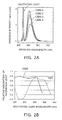
- FIGS. 2A and 2B are graphs showing the characteristics of the phosphor 31 according to First Embodiment.
- FIG. 2A shows the emission spectra of the phosphor 31.
- the horizontal axis represents emission wavelength, and the vertical axis represents emission intensity (arbitrary unit).
- FIG. 2B shows the excitation spectrum of the phosphor 31.
- the horizontal axis represents a wavelength of the excitation light, and the vertical axis represents relative absorption of the excitation light.
- FIG. 3 is a graph comparing the emission spectra of the phosphor 31 and a YAG phosphor.
- the horizontal axis represents a wavelength of the emission light, and the vertical axis represents relative emission intensity.
- the phosphor 31 is represented by the chemical formula Ca 8-x Eu x Mg 1-y Mn y (SiO 4 ) 4 Cl 2 (0 ⁇ x ⁇ 8, 0 ⁇ y ⁇ 1), and is obtained by adding Eu to calcium magnesium chlorosilicate (hereinafter, "CMS phosphor").
- CMS phosphor calcium magnesium chlorosilicate
- the proportion y of manganese (Mn) is desirably in the range of 0 ⁇ y ⁇ 0.2.
- FIG. 2A shows the emission spectra of CMS phosphors containing europium (Eu) in different contents.
- CMS1 to CMS4 do not represent a first phosphor as comprised in the claimed light emitting device
- the emission peak wavelength ⁇ p of the CMS phosphor shifts towards the longer wavelength side with increase in the proportion of europium (Eu) in the composition.
- FIG. 2B shows the excitation light absorption characteristic of the CMS phosphor (i.e. wavelength dependence thereof). The graph also shows the excitation light absorption characteristic of a YAG phosphor for comparison.
- the CMS phosphor absorbs light of 480 nm or shorter wavelengths, and emits fluorescence in a wavelength range of 490 nm to 650 nm, wherein absorption of the excitation light may increase as approaching a wavelength of 370 nm from 450 nm in the composition range described above. Owing to small self-absorption, the CMS phosphor has high radiation efficiency.
- the emission peak intensity of the CMS phosphor may be at least twice as high as that of the YAG phosphor, as shown in FIG. 3 .
- the CMS phosphor By comparing the excitation light absorption characteristics of the CMS phosphor and the YAG phosphor, the CMS phosphor exhibits smaller change of absorptance than the YAG phosphor, which depends on a wavelength of the excitation light.
- the absorptance change is particularly smaller in the wavelength range of 460 nm or less, and the emission intensity also exhibits only a small change as varying excitation wavelengths in this wavelength range.
- FIG. 4 is a graph showing the characteristics of other examples of the phosphor 31 according to First Embodiment.
- the phosphors 31 shown in FIG. 4 are CMS phosphors having the compositions in which the constituent magnesium (Mg) is partially substituted with manganese (Mn).
- the chemical formulae of the CMS phosphors 5 to 8 shown in FIG. 4 , and the wavelengths of the corresponding emission peaks of these compositions are as follows.
- the CMS phosphor may vary its emission peak wavelength even with the partial substitution of magnesium (Mg) with manganese (Mn).
- the phosphor 31 may thus absorb, for example, the excitation light of 450 nm wavelength, and emit fluorescence having the intensity peak in a wavelength range of 500 nm to 555 nm.
- the luminosity curve of human has a maximum value at the light wavelength of 555 nm, and the phosphor 31 has the emission peak on the shorter wavelength side from the light wavelength at which the luminosity factor becomes maximum value.
- the inventors have found that the CMS phosphor with the chemical formula Ca 8-x Eu x Mg 1-y Mn y (SiO 4 ) 4 Cl 2 (0 ⁇ x ⁇ 8, 0 ⁇ y ⁇ 1) exhibits only a small change of absorptance in the wavelength range of 460 nm or less, and it is possible to suppress a variation of the emission intensity in the light emitting device 1 due to a wavelength change of the excitation light in the range of 460 nm or less, when the CMS phosphor is used as the phosphor 31.
- the emission wavelength of the blue light-emitting diode is preferably in the range of 365 nm to 470 nm. Down to the shortest wavelength of 365 nm, In x Ga 1-x N (0 ⁇ x ⁇ 1) may keep high-efficiency of the blue light emission, and the CMS phosphor may absorb the excitation light up to the wavelength of 470 nm. Considering low-temperature operations, it is preferable for a high-efficiency light emitting device to use a blue light-emitting diode that emits light in the wavelength range of 360 nm to 470 nm.
- the structure and the manufacturing method of the light emitting device 1 are described below in detail with reference to FIG. 5A to FIG. 12B .
- FIG. 5A is a graph showing an exemplary emission spectrum of the light emitting device 1 according to the first embodiment.
- the stacked body 15 is a blue light-emitting diode having the emission peak at the wavelength of 450 nm.
- the phosphor layer 30 includes a second phosphor (hereinafter, phosphor 33) that is excited by light radiated from the stacked body 15, and, in some cases, partially by the fluorescence of the phosphor 31.
- the phosphor 33 emits light having the emission peak on the longer wavelength side than the emission peak wavelength of the phosphor 31. In this way, a white light source can be realized with a desired color temperature.
- the phosphor 33 is, for example, an orange phosphor having the emission peak in the wavelength range of 580 nm to 600 nm.
- the emission spectrum shown in FIG. 5A includes the emission peak of phosphor 31 in the wavelength range of blue green color and the emission peak of the phosphor 33 in the wavelength range of orange color in addition to the emission peak of excitation light in the blue light range.
- the emission peaks of phosphors 31 and 33 locate on both sides of the peak at the wavelength of 555 nm in the luminosity curve of human. As shown in FIG.
- this makes it possible to achieve brightness by the spectral components that locate on both sides of the peak within a range of the luminosity curve that is equivalent to the isochromatic curve y in the xyz isochromatic curves, and to ensure high degree of color rendition with the relatively broad emission spectrum that is close to the sunlight spectrum (color rendering index Ra 100) broader than the luminosity curve. This makes it easier to satisfy both requirements for higher emission efficiency and higher level color rendition as compared to the conventional phosphors having emission peaks in the green to yellow range.
- the emission peak may coincide with the peak of the isochromatic curve y.
- adjusting the brightness i.e. y coordinate
- red light is necessary in a white light spectrum using the conventional phosphor, to improve color rendition.
- the red light may include a large spectral component outside the isochromatic curve y that is equivalent to the human luminosity curve, and has less contribution to brightness.
- the CMS phosphor it is possible with the CMS phosphor to adjust the integral amount of the isochromatic curve y almost independently from the isochromatic curve x. This makes it possible to ensure the integral amount of the isochromatic curve y for high brightness, and to adjust chromaticity while maintaining high brightness and high level color rendition. That is, chromaticity can be flexibly adjusted with maintaining high brightness and high level color rendition. Thereby, the white light source may be achieved with high brightness and high level color rendition.
- the embodiment is not limited to the light emitting device 1 having the emission spectrum shown in FIGS. 5A and 5B , and a red phosphor, a yellow phosphor, or a green phosphor, or a mixture thereof each cited below may be used for the phosphor 33.
- the orange to red phosphors may contain, for example, at least one of a nitride phosphor CaAlSiN 3 :Eu, a (Ba,Sr) 3 SiO 5 :Eu phosphor, a (Ba,Sr) 3 (Si,Ge)O 5 :Eu phosphor or a solid solution thereof with Al, and a sialon phosphor.
- the light emitting device 1 having high brightness and high level color rendition may be achieved by the phosphor layer 30 containing single-phase crystals of (Ba,Sr) 3 SiO 5 :Eu or (Ba,Sr) 3 (Si,Ge)O 5 :Eu, and the CMS phosphor.
- a phosphor of strontium silicate system which is represented by the chemical formula of (Sr 1-x-y Ba y Eu x ) 3 (Si 1-z Ge z )O 5 (0 ⁇ x ⁇ 0.1, 0 ⁇ y ⁇ 1, 0 ⁇ z ⁇ 0.1), may be used for the phosphor layer 30.
- a (Sr 0.97 Eu 0.03 ) 3 SiO 5 phosphor which has an emission peak at a wavelength of 580 nm
- a (Sr 0.845 Ba 0.125 E 0.30 ) 3 SiO 5 phosphor which has an emission peak at a wavelength of 600 nm
- examples may be referred to as examples.
- strontium silicate phosphors described above do not absorb the light emitted from the CMS phosphor, and thus, make it possible to achieve a light source which has higher light emission efficiency, and exhibits higher level color rendition than those in the case using the nitride phosphor CaAlSiN 3 :Eu, which absorbs the light emitted from the CMS phosphor.
- FIG. 15 is a graph showing an emission spectrum EB of the light emitting device 1.
- FIG. 15 also includes an emission spectrum CE of a light emitting device according to a relative example, wherein the YAG phosphor is used, and the dark-field luminosity curve yd.
- the emission spectrum EB shown in FIG. 15 includes a blue light of wavelength 450 nm and emissions of CMS phosphor and strontium silicate phosphor, wherein the emission spectrum of the CMS phosphor includes an emission peak at the wavelength of 512 nm, and the emission spectrum of the strontium silicate phosphor includes an emission peak 580 nm.
- the light emitting device 1 with the emission spectrum EB exhibits the color rendering index Ra of 90.
- the emission spectrum CE includes a blue light of wavelength 450 nm and an emission of YAG phosphor, wherein the emission spectrum of the YAG phosphor includes a broad peak in the wavelength range of 530 nm ⁇ 620 nm.
- the light emitting device with the emission spectrum CE exhibits Ra of 80.
- the dark-field luminosity curve yd shown in FIG. 15 has a luminosity peak at a wavelength of 507 nm.
- the emission peak wavelength of the CMS phosphor locates in vicinity of the luminosity peak wavelength in the luminosity curve yd.
- Such a device may be advantageous in use of the street and tunnel.
- the sialon phosphor is represented by, for example, the chemical formula (M 1-x ,R x ) a1 AlSi b1 O c1 N d1 .
- M is at least one metal element excluding Si and Al, and is preferably at least one of Ca and Sr.
- R is the emission center element, and is preferably, for example, Eu.
- the symbols of x, a1, b1, c1, and d1 satisfy the following relations. 0 ⁇ x ⁇ 1 ; 0.6 ⁇ a 1 ⁇ 0.95 ; 2 ⁇ b 1 ⁇ 3.9 ; 0.25 ⁇ c 1 ⁇ 0.45 ; and 4 ⁇ d 1 ⁇ 5.7
- the phosphor used in the color range of orange to red is not limited to ones described above.
- the yellow phosphor may contain, for example, at least one of YAG phosphor, silicate phosphor (Sr,Ca,Ba) 2 SiO 4 :Eu, La 3 Si 6 N 11 :Ce 3+ phosphor, Li 2 SrSiO 4 :Eu, and BOSE phosphor (Ba,Sr) 2 SiO 4 :Eu.
- the composition rates of x, y and z are preferably in the ranges of 0 ⁇ x ⁇ 1, 0.01
- the green phosphor may contain, for example, at least one of halophosphate phosphor (Ba,Ca,Mg) 10 (PO 4 ) 6 ⁇ Cl 2 :Eu, silicate phosphor (SrBa) 2 SiO 4 :Eu, YAG phosphor Y 3 Al 5 O 12 :Ce, LAG phosphor Lu 3 Al 5 O 12 :Ce, and sialon phosphor.
- ⁇ p 512 nm
- the LAG phosphor is represented by a chemical formula of (Lu 1-x A x ) 3 (Al 1-x By) 5 (O 1-z C z ) 12 (0 ⁇ x ⁇ 1, 0 ⁇ y ⁇ 1, 0 ⁇ z ⁇ 1), wherein A is one element selected from a group of Y, Tb, Gd, Sm, La, Sr, Ba, Ca and Mg; B is one element selected from a group of Si, Ge, B, P and Ga; and C is one element selected from a group of F, Cl, N and S.
- the composition rates of x, y and z are preferably in the ranges of 0 ⁇ x ⁇ 1, 0.01 ⁇ y ⁇ 0.2, and 0.001 ⁇ z ⁇ 0.2.
- the sialon phosphor is represented by, for example, the chemical formula (M 1-x ,R x ) a2 AlSi b2 O c2 N d2 .
- M is at least one metal element excluding Si and Al, and is preferably at least one of Ca and Sr.
- R is the emission center element, and is preferably, for example, Eu.
- the symbols of x, a2, b2, c2, and d2 satisfy the following relations. 0 ⁇ x ⁇ 1 ; 0.93 ⁇ a 2 ⁇ 1.3 ; 4.0 ⁇ b 2 ⁇ 5.8 ; 0.6 ⁇ c 2 ⁇ 1 ; and 6 ⁇ d 2 ⁇ 11
- the peak wavelength of the light radiated from the stacked body 15 may be shorter than 360 nm. It is also favorable in this case to dispose a phosphor that has an emission peak on the longer wavelength side than the peak wavelength of 550 nm in the human luminosity curve.
- the light emitting device 1 may lack blue light in the emission spectrum. It is therefore desirable to add a blue phosphor (third phosphor) having an emission peak in a wavelength range of 430 nm to 480 nm.
- a blue phosphor (third phosphor) having an emission peak in a wavelength range of 430 nm to 480 nm.
- an oxide phosphor such as BaMgAl 10 O 17 :Eu and Sr 3 MgSi 2 O:Eu, (Sr,Ca,Ba,Mg) 5 (PO 4 ) 3 Cl:Eu, (Sr,Ca,Ba,Mg) 10 (PO 4 ) 6 Cl 2 :Eu or the like may be used for the third phosphor.
- red, yellow, and green phosphors that have high excitation efficiency in a wavelength range shorter than 360 nm.
- Such a red phosphor is, for example, Y 2 O 3 :Eu, (Y,Gd)BO 3 :Eu, Y 2 O 2 S:Eu, Gd 2 O 2 S:Eu, La 2 O 2 S:Eu, (SrBa) 3 MgSi 2 O 8 :EuMn, 3.5MgO ⁇ 0.5MgF 2 .GeO 2 :Mn, or LiEuW 2 O 8 .
- the yellow phosphor is, for example, (Ca,Sr) 5 (PO 4 ) 3 Cl:EuMn, (Sr,Ba) 3 MgSi 2 O 8 :EuMn, or Zn 2 GeO 4 :Mn.
- the green phosphor is, for example, (Ca,Sr) 5 (PO 4 ) 3 Cl:EuMn, BaMgAl 10 O 17 :EuMn, LaAl(SiAl) 6 N 9 O:Ce, (SrBa) 3 MgSi 2 O 8 :EuMn, LaPO 4 :CeTb, or CeMgAl 11 O 19 :Tb.
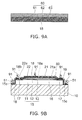
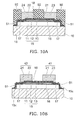
- FIG. 6A to FIG. 12B are schematic cross sectional views showing a manufacturing process of the light emitting device according to the first embodiment.
- the n-type semiconductor layer 11 (first semiconductor layer), the light emitting layer 13, and the p-type semiconductor layer 12 (second semiconductor layer) are epitaxially grown in this order on the major surface of a substrate 10 by using, for example, MOCVD (metal organic chemical vapor deposition).
- MOCVD metal organic chemical vapor deposition
- a semiconductor layer 115 is formed on the substrate 10, wherein the semiconductor layer 115 includes the n-type semiconductor layer 11, the light emitting layer 13, and the p-type semiconductor layer 12.
- a surface of the semiconductor layer 115 on the substrate 10 side is a first surface 15a, and a surface opposite thereto is a second surface 15b.
- the first surface 15a is also described as a light emitting surface.
- the substrate 10 is, for example, a silicon substrate.
- the substrate 10 may be a sapphire substrate, or a silicon carbide (SiC) substrate.
- the semiconductor layer 115 is, for example, made of nitride semiconductors such as Group III nitride compound semiconductor.
- the n-type semiconductor layer 11 includes, for example, a buffer layer provided on the major surface of the substrate 10, and an n-type GaN layer provided on the buffer layer.
- the p-type semiconductor layer 12 may include, for example, a p-type AlGaN layer provided on the light emitting layer 13, and a p-type GaN layer provided on the p-type AlGaN layer.
- the light emitting layer 13 has, for example, an MQW (multiple quantum well) structure.
- the light emitting layer 13 emits light having an emission peak, for example, in the wavelength range of 360 nm to 470 nm.
- the light emitting layer 13 may emits light having an emission peak, for example, in the wavelength range of 360 nm or less.
- FIG. 6B shows the semiconductor layer 115 after selectively removing the p-type semiconductor layer 12 and the light emitting layer 13.
- the p-type semiconductor layer 12 and the light emitting layer 13 are selectively etched by RIE (reactive ion etching) to expose the n-type semiconductor layer 11.
- the n-type semiconductor layer 11 is selectively removed to form a trench 90.
- the trench 90 divides the semiconductor layer 115 into a plurality of stacked bodies 15 on the substrate 10.
- the stacked bodies 15 each serve as a light emitter including the light emitting layer 13.
- the trench 90 is formed, for example, in a shape of grid (not illustrated).
- the trench 90 is formed through the semiconductor layer 115, and reaches to the substrate 10.
- the substrate 10 may also be etched so that the bottom of the trench 90 locates at lower level than the interface between the substrate 10 and the semiconductor layer 115.
- the trench 90 may be formed after forming a p-side contact electrode 16 and an n-side electrode 17.
- the p-side electrode 16 is formed on the p-type semiconductor layer 12, as shown in FIG. 7B .
- the n-side electrode 17 is formed on a portion of the n-type semiconductor layer 11 where the p-type semiconductor layer 12 and the light emitting layer 13 have been selectively removed.
- the p-side electrode 16 formed on the p-type semiconductor layer 12 may include a reflecting material that reflects the light emitted from the light emitting layer 13.
- the p-side electrode 16 includes silver, silver alloy, aluminum, aluminum alloy, or the like.
- the p-side electrode 16 may include a metal protective film (i.e. barrier metal) for suppressing sulfurization and oxidation thereof.
- An insulating film 18 is formed to cover the structure formed on the substrate 10, as shown in FIG. 8A .
- the insulating film 18 covers the second surface 15b side, and the p-side electrode 16 and the n-side electrode 17.
- the insulating film 18 also covers side surfaces 15c joined to the first surface 15a.
- the insulating film 18 is also formed on a surface of the substrate 10 at the bottom of the trench 90.
- the insulating film 18 is, for example, a silicon oxide film or silicon nitride film formed by CVD (chemical vapor deposition). As shown in FIG. 8B , the insulating film 18 has first openings 18a and a second opening 18b formed, for example, by wet etching using a resist mask. The first openings 18a are in communication with the p-side electrode 16, and the second opening 18b is in communication with the n-side electrode 17. Alternatively, a first opening 18a of larger size may be provided as a single opening over the p-side electrode 16.
- a underlying metal layer 60 is formed on the insulating film 18, the inner surfaces (the side walls and bottom surfaces) of the first openings 18a, and the inner surface (the side wall and bottom surface) of the second opening 18b.
- the underlying metal layer 60 includes an aluminum film 61, a titanium film 62, and a copper film 63.
- the aluminum film 61 serves as a reflecting film.
- the copper film 63 serves as a seed for plating.
- the titanium film 62 is suitable in wettability for both aluminum and copper, and serves as an adhesive layer.
- the underlying metal layer 60 is formed by, for example, sputtering.
- a resist mask 91 is selectively formed on the underlying metal layer 60, as shown in FIG. 9B , and a p-side interconnection layer 21, an n-side interconnection layer 22, and a metal film 51 are formed by electrolytic copper plating, using the copper film 63 of the underlying metal layer 60 as a seed film.
- the p-side interconnection layer 21 is also formed inside the first openings 18a, and is electrically connected to the p-side electrode 16.
- the n-side interconnection layer 22 is also formed inside the second opening 18b, and is electrically connected to the n-side electrode 17.
- the resist mask 91 is removed by using, for example, a solvent or an oxygen plasma, and then, a resist mask 92 is selectively formed on the plating layers 21, 22 and 51, as shown in FIG. 10A .
- the resist mask 92 may be formed without removing the resist mask 91.
- a p-side metal pillar 23, and an n-side metal pillar 24 are formed by electrolytic copper plating, using the p-side interconnection layer 21 and the n-side interconnection layer 22 as seed layers.
- the p-side metal pillar 23 is formed on the p-side interconnection layer 21.
- the p-side interconnection layer 21 and the p-side metal pillar 23 are joined into one body, when using the same copper material therefor.
- the n-side metal pillar 24 is formed on the n-side interconnection layer 22.
- the n-side interconnection layer 22 and the n-side metal pillar 24 are joined into one body when using the same copper material therefor.
- the resist mask 92 is removed by a solvent or an oxygen plasma, for example.
- the p-side interconnection layer 21 and the n-side interconnection layer 22 are electrically connected to each other via the underlying metal layer 60.
- the p-side interconnection layer 21 and the metal film 51 are also electrically connected to each other via the underlying metal layer 60.
- the n-side interconnection layer 22 and the metal film 51 are also electrically connected to each other via the underlying metal layer 60.
- the underlying metal layer 60 is removed by etching in portions between the p-side interconnection layer 21 and the n-side interconnection layer 22, the p-side interconnection layer 21 and the metal film 51, and the n-side interconnection layer 22 and the metal film 51, as shown in FIG. 10B .
- the electrical connections vanishes between the p-side interconnection layer 21 and the n-side interconnection layer 22, the p-side interconnection layer 21 and the metal film 51, and the n-side interconnection layer 22 and the metal film 51.
- the p-side interconnection layer 21 and the p-side metal pillar 23 form the p-side interconnect electrode 41.
- the n-side interconnection layer 22 and the n-side metal pillar 24 form the n-side interconnect electrode 43.
- the metal film 51 formed on the side surfaces 15c of the stacked body 15 is electrically floating, and does not serve as an electrode.
- the metal film 51 preferably serves as a reflecting film. The reflectivity of the metal film 51 may be increased by including at least the aluminum film 61.
- the p-side interconnect electrode 41 and the n-side interconnect electrode 43 By using copper as material of the p-side interconnect electrode 41 and the n-side interconnect electrode 43 as above, it is possible to achieve desirable heat conduction and high migration resistance, and improve adhesion for the insulating material.
- the embodiment is not limited to this example, and, for example, materials such as gold, nickel, and silver may be used for the p-side interconnect electrode 41 and the n-side interconnect electrode 43.
- the resin layer 25 shown in FIG. 11A is formed on the structure shown in FIG. 10B .
- the resin layer 25 covers the p-side interconnect electrode 41 and the n-side interconnect electrode 43.
- the resin layer 25 also covers the metal film 51.
- materials having the same or similar coefficient of thermal expansion to the mounting substrate are used for the resin layer 25.
- Such material used for the resin layer 25 is primarily composed of epoxy resin, silicone resin, or fluororesin, for example. It is preferable to add a light shielding material (such as light absorbing particles, light reflecting particles, and light scattering particles) to the resin layer 25 to shield the emission from the light emitting layer 13. This makes it possible to suppress a light leak from the side surfaces and the mounting surface of the support body 100.
- the support body 100 maintains the stacked bodies 15 in a wafer shape.
- the substrate (silicon substrate) 10 may be removed by wet etching or dry etching.
- a laser lift-off method may be used when the substrate 10 is a sapphire substrate.
- the stacked body 15 on the substrate 10 may involve a large internal stress through the epitaxial growth.
- the p-side metal pillar 23, the n-side metal pillar 24, and the resin layer 25 are more flexible than the stacked body 15 made of, for example, a GaN material. Accordingly, the p-side metal pillar 23, the n-side metal pillar 24, and the resin layer 25 may absorb the internal stress, when removing the substrate 10. Hence, it is possible to avoid the stacked body 15 being damaged during the process of removing the substrate 10.
- Removing the substrate 10 exposes the first surface 15a of the stacked body 15, as shown in FIG. 11B .
- Microscopic irregularities are formed on the first surface 15a.
- the stacked body 15 is wet etched on the first surface 15a side with a KOH (potassium hydroxide) aqueous solution, TMAH (tetramethylammonium hydroxide), or the like.
- KOH potassium hydroxide
- TMAH tetramethylammonium hydroxide
- the etching rate thereof that depends on the crystal orientation of the stacked body 15 forms irregularities corresponding to the microscopic crystal structure in the first surface 15a.
- the microscopic irregularities on the first surface 15a may improve light extraction efficiency from the stacked body 15.
- a phosphor layer 30 is formed on the first surface 15a via an insulating film 19 of material such as SiO 2 and SiN, as shown in FIG. 12A .
- the phosphor layer 30 includes at least the phosphor 31, as described above.
- the phosphor layer 30 may contain other phosphors, including the phosphor 33 described above.
- the phosphor layer 30 is formed by using methods, for example, such as printing, potting, molding, and compression molding.
- the insulating film 19 improves the adhesion strength between the stacked body 15 and the phosphor layer 30.
- the phosphor layer 30 may be bonded via the insulating film 19, which is a sintered body prepared by sintering a phosphor with a binder, or a resin sheet including a phosphor.
- the resin layer 25 is also provided around the side surfaces 15c of the stacked body 15.
- the phosphor layer 30 is formed extending on the region around the side surfaces 15c of the stacked body 15. Part of the phosphor layer 30 is formed on the resin layer 25 via the insulating films 18 and 19.
- the resin layer 25 is ground on a side opposite to the phosphor layer 30 to expose the p-side metal pillar 23 and the n-side metal pillar 24 in a surface of the resin layer 25 (the lower surface side in FIG. 12A ), as shown in FIG. 12B .
- the exposed surface of the p-side metal pillar 23 is a p-side external terminal 23a
- the exposed surface of the n-side metal pillar 24 is an n-side external terminal 24a.
- the wafer is divided into pieces by dicing along the trench 90 separating the stacked bodies 15 from each other.
- the phosphor layer 30, the insulating film 19, the insulating film 18, and the resin layer 25 are cut, for example, by a dicing blade, or a laser beam. Since the stacked bodies 15 are absent in the dicing regions, it is possible to avoid the stacked body being damaged through the dicing process.
- Each light emitting device 1 includes at least one stacked body 15.
- the light emitting device 1 may have a single-chip structure with one stacked body 15, or a multiple-chip structure with more than one stacked body 15.
- the light emitting device 1 according to the embodiment is a micro device that includes the stacked body 15 and the phosphor layer 30 in a chip size package.
- the stacked bodies 15 are maintained in the wafer shape.
- the manufacturing steps before the dicing are performed in the wafer state, and the dicing completes the light emitting device 1. This makes the manufacturing cost being greatly reduced.
- the p-side external terminal 23a and the n-side external terminal 24a exposed in the surface of the resin layer 25 are bonded to land patterns on the mounting substrate, for example, via conductive materials such as solders.
- the p-side metal pillar 23, the n-side metal pillar 24, and the resin layer 25 may absorb and relieve the thermal cycle-induced stress between the light emitting device 1 and the mounting substrate. This enables to prevent the emission characteristics of the light emitting device 1 from deterioration, and improves the device reliability.
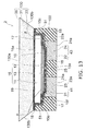
- FIG. 13 is a schematic cross sectional view showing a light emitting device 2.
- the light emitting device 2 includes a stacked body 15, and a phosphor layer 130 provided on a light emitting surface of the stacked body 15. It differs from the light emitting layer 1 in the shape of the phosphor layer 130.
- a support body 100 including a p-side interconnect electrode 41, an n-side interconnect electrode 43, and a resin layer 25 is provided on the second surface 15b side of the stacked body 15.
- the support body 100 provided on the second surface 15b side supports the light emitting element (i.e. LED chip) containing the stacked body 15, the p-side electrode 16, and the n-side electrode 17.
- the phosphor layer 130 includes, for example, phosphors 31 and 33 of particle shapes.
- the phosphors 31 and 33 are excited by light emitted from the light emitting layer 13, and emit lights with wavelengths different from that of light emitted from the light emitting layer 13.
- the phosphors 31 and 33 are joined into one body with a binder 35.
- the binder 35 transmits the lights emitted from the light emitting layer 13 and the phosphor 31.
- the word "transmit" here is not limited to transmit 100% of light, and may include the case where the light is partially absorbed in the binder 35.
- the phosphor layer 130 is provided so that side surfaces 130b are inclined with respect to the first surface 15a of the stacked body 15, and the upper surface 130a of the phosphor layer 130.
- the side surfaces 130b of the phosphor layer 130 form an obtuse angle with respect to the first surface 15a. Specifically, the inner angle ⁇ created by the first surface 15a and the side surfaces 130b is greater than 90°.
- the plane area of cross-section in parallel to the first surface 15a gradually increases in the phosphor layer 130 towards the upper surface 130a side from the first surface 15a side.
- the side surfaces 130b of the phosphor layer 130 are on the outer side than the side surfaces of the support body 100 (i.e. side surfaces of the resin layer 25) in the direction perpendicular to the first surface 15a.
- Such shape of the phosphor layer 130 may be formed by cutting the wafer, for example, with a blade having a V-shape tip.
- the side surfaces 130b of the phosphor layer 130 are formed to be substantially flat without irregularities intended to improve light extraction efficiency by light scattering effect.
- the lights that are emitted from the light emitting layer 13 and the phosphor 31, and propagate towards the side surfaces 130b are incident on the side surfaces 130b at a larger angle, and thus, parts of the lights increases, which is totally reflected at the side surfaces 130a toward the upper surface 130a side.
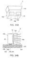
- FIGS. 14A and 14B are schematic cross sectional views showing a light emitting device 3 according to a variation of the second embodiment.
- FIG. 14A is a schematic perspective view of the light emitting device 3.
- FIG. 14B is a schematic cross sectional view of a light emitting module including the light emitting device 3 mounted on a substrate 310.
- the first embodiment is also applicable to the light emitting device 3 of a side-view type shown in FIGS. 14A and 14B .
- the light emitting device 3 has the same structure as the light emitting device 2, except for the exposed surfaces of the metal pillars 23 and 24 provided for external connections.
- the side surface of the p-side meal pillar 23 is partially exposed from the resin layer 25 in a third surface 25b that has a plane orientation different from the first surface 15a of the stacked body 15 and the second surface 15b opposite to the first surface 15a.
- the exposed surface serves as a p-side external terminal 23b for mounting on an external substrate 310.
- the third surface 25b is a surface substantially perpendicular to the first surface 15a and the second surface 15b.
- the resin layer 25 has four side surfaces, and one of these side surfaces is the third surface 25b.
- the side surface of the n-side metal pillar 24 is partially exposed from the resin layer 25 in the third surface 25b.
- the exposed surface serves as an n-side external terminal 24b for mounting on the external substrate 310.
- the p-side metal pillar 23 is covered with the resin layer 25 except for the p-side external terminal 23b exposed on the third surface 25b.
- the n-side metal pillar 24 is covered with the resin layer 25 except for the n-side external terminal 24b exposed on the third surface 25b.
- the light emitting device 3 is mounted with the third surface 25b facing the mounting surface 301 of the substrate 310, as shown in FIG. 14B .
- the p-side external terminal 23b and the n-side external terminal 24b exposed on the third surface 25b are bonded to pads 302 provided on the mounting surface 301, using a solder 303.
- the substrate 310 also includes, for example, a wiring pattern provided on the mounting surface 301, and leading to an external circuit. The wiring pattern connects the pads 302 and the external circuit.
- the third surface 25b is substantially perpendicular to the first surface 15a that is the light emitting surface.
- the first surface 15a thus faces a lateral direction parallel to the mounting surface 301, or a direction tilted with respect to the mounting surface 301, wherein the third surface 25b faces the mounting surface 301. That is,
- the light emitting device 3 is the side view-type light emitting device which emits light in a lateral direction parallel to the mounting surface 301, or in an oblique direction with respect to the mounting surface 301.
- the phosphor layer 130 shown on FIGS. 14A and 14B may be replaced by the phosphor layer 30 of the first embodiment. That is, the phosphor layer 130 may also include phosphors cited in the first embodiment.
- the "nitride semiconductor” referred to herein includes group III-V compound semiconductors of B x In y Al z Ga 1-x-y-z N (0 ⁇ x ⁇ 1, 0 ⁇ y ⁇ 1, 0 ⁇ z ⁇ 1, 0 ⁇ x+y+z ⁇ 1), and also includes mixed crystals containing a group V element besides N (nitrogen), such as phosphorus (P) and arsenic (As). Furthermore, the “nitride semiconductor” also includes those further containing various elements added to control various material properties such as conductivity type, and those further containing various unintended elements.
Landscapes
- Chemical & Material Sciences (AREA)
- Inorganic Chemistry (AREA)
- Engineering & Computer Science (AREA)
- Materials Engineering (AREA)
- Organic Chemistry (AREA)
- Led Device Packages (AREA)
- Led Devices (AREA)
- Luminescent Compositions (AREA)
Claims (12)
- Lichtemittierende Vorrichtung (1, 2, 3), umfassend:einen Lichtemitter (15), der ein Emissionsmaximum in einem Wellenlängenbereich von nicht weniger als 360 Nanometer und nicht mehr als 470 Nanometer aufweist; undeinen ersten Leuchtstoff (31) mit einer Zusammensetzung mit der chemischen Formel Ca8-xEuxMg1-yMny(SiO4)4Cl2, worin 0 < x ≤ 8, 0 < y ≤ 1 ist.
- Vorrichtung gemäß Anspruch 1, wobei der Anteil y des in dem ersten Leuchtstoff (31) enthaltenen Mangans nicht mehr als 0,2 ist.
- Vorrichtung gemäß Anspruch 1, zusätzlich umfassend einen zweiten Leuchtstoff (33) mit einem Emissionsmaximum in einem Wellenlängenbereich länger als 555 Nanometer.
- Vorrichtung gemäß Anspruch 3, zusätzlich umfassend eine Schicht, die den Lichtemitter (15) bedeckt,
wobei die Schicht den ersten Leuchtstoff (31) und den zweiten Leuchtstoff (33) beinhaltet. - Vorrichtung gemäß Anspruch 3, wobei das Emissionsmaximum des zweiten Leuchtstoffs (33) in einem Wellenlängenbereich von nicht weniger als 580 Nanometer und nicht mehr als 600 Nanometer liegt.
- Vorrichtung gemäß Anspruch 3, wobei der zweite Leuchtstoff (33) einen Leuchtstoff aus einem Strontiumsilicat-System enthält.
- Vorrichtung gemäß Anspruch 3, wobei der zweite Leuchtstoff (33) einen Leuchtstoff mit einer chemischen Formel (Sr1-x-yBayEux)3 (Si1-zGez)O5 enthält, worin 0 < x ≤ 0,1, 0 ≤ y ≤ 1 und 0 ≤ z ≤ 0,1 ist.
- Lichtemittierende Vorrichtung (1, 2, 3), umfassend:einen Lichtemitter (15), der ein Emissionsmaximum in einem Wellenlängenbereich kürzer als 360 Nanometer aufweist;einen ersten Leuchtstoff (31) mit einer Zusammensetzung mit der chemischen Formel Ca8-xEuxMg1-yMny(SiO4)4Cl2, worin 0 < x ≤ 8, 0 < y ≤ 1 ist, mit einem Emissionsmaximum in einem Wellenlängenbereich von nicht weniger als 500 Nanometer und nicht mehr als 555 Nanometer; undeinen zweiten Leuchtstoff (33) mit einem Emissionsmaximum in einem Wellenlängenbereich länger als 555 Nanometer.
- Vorrichtung gemäß Anspruch 8, wobei der Anteil y des in dem ersten Leuchtstoff (31) enthaltenen Mangans nicht mehr als 0,2 ist.
- Vorrichtung gemäß Anspruch 8, wobei das Emissionsmaximum des zweiten Leuchtstoffs (33) in einem Wellenlängenbereich von nicht weniger als 580 Nanometer und nicht mehr als 600 Nanometer liegt.
- Vorrichtung gemäß Anspruch 8, zusätzlich umfassend einen dritten Leuchtstoff (33) mit einem Emissionsmaximum in einem Wellenlängenbereich von nicht weniger als 430 Nanometer und nicht mehr als 480 Nanometer.
- Vorrichtung gemäß Anspruch 8, wobei der zweite Leuchtstoff (33) einen Leuchtstoff mit einer chemischen Formel (Sr1-x-yBayEux)3(Si1-zGez)O5 enthält, worin 0 < x ≤ 0,1, 0 ≤ y ≤ 1 und 0 ≤ z ≤ 0,1 ist.
Applications Claiming Priority (2)
| Application Number | Priority Date | Filing Date | Title |
|---|---|---|---|
| JP2014049086 | 2014-03-12 | ||
| JP2014167554A JP2015188050A (ja) | 2014-03-12 | 2014-08-20 | 発光装置 |
Publications (2)
| Publication Number | Publication Date |
|---|---|
| EP2918655A1 EP2918655A1 (de) | 2015-09-16 |
| EP2918655B1 true EP2918655B1 (de) | 2016-10-26 |
Family
ID=51494121
Family Applications (1)
| Application Number | Title | Priority Date | Filing Date |
|---|---|---|---|
| EP14183718.7A Active EP2918655B1 (de) | 2014-03-12 | 2014-09-05 | Lichtemittierende vorrichtung |
Country Status (4)
| Country | Link |
|---|---|
| US (1) | US20150263244A1 (de) |
| EP (1) | EP2918655B1 (de) |
| JP (1) | JP2015188050A (de) |
| TW (1) | TWI559579B (de) |
Families Citing this family (5)
| Publication number | Priority date | Publication date | Assignee | Title |
|---|---|---|---|---|
| JP6772621B2 (ja) * | 2016-07-27 | 2020-10-21 | 日亜化学工業株式会社 | 発光装置 |
| TWI720053B (zh) * | 2016-11-09 | 2021-03-01 | 晶元光電股份有限公司 | 發光元件及其製造方法 |
| TWI764528B (zh) * | 2016-11-09 | 2022-05-11 | 晶元光電股份有限公司 | 發光元件及其製造方法 |
| US12439747B2 (en) * | 2019-04-24 | 2025-10-07 | PlayNitride Display Co., Ltd. | Micro device and display apparatus |
| WO2024143215A1 (ja) * | 2022-12-27 | 2024-07-04 | 日亜化学工業株式会社 | 発光装置 |
Family Cites Families (11)
| Publication number | Priority date | Publication date | Assignee | Title |
|---|---|---|---|---|
| US6504179B1 (en) * | 2000-05-29 | 2003-01-07 | Patent-Treuhand-Gesellschaft Fur Elektrische Gluhlampen Mbh | Led-based white-emitting illumination unit |
| WO2004085570A1 (en) * | 2003-03-28 | 2004-10-07 | Korea Research Institute Of Chemical Technology | Strontium silicate-based phosphor, fabrication method thereof, and led using the phosphor |
| KR100605211B1 (ko) * | 2004-04-07 | 2006-07-31 | 엘지이노텍 주식회사 | 형광체 및 이를 이용한 백색 발광다이오드 |
| DE102004038199A1 (de) * | 2004-08-05 | 2006-03-16 | Patent-Treuhand-Gesellschaft für elektrische Glühlampen mbH | LED mit niedriger Farbtemperatur |
| JP5323308B2 (ja) * | 2006-09-19 | 2013-10-23 | 株式会社小糸製作所 | 発光モジュール |
| JP5360857B2 (ja) * | 2007-05-17 | 2013-12-04 | Necライティング株式会社 | 緑色発光蛍光体、その製造方法及びそれを用いた発光素子 |
| JP2009040918A (ja) * | 2007-08-09 | 2009-02-26 | Mitsubishi Chemicals Corp | 蛍光体及びその製造方法、蛍光体含有組成物、発光装置、並びに画像表示装置及び照明装置 |
| WO2011022399A1 (en) * | 2009-08-17 | 2011-02-24 | Osram Sylvania Inc. | Phosphor blend for an led light source and led light source incorporating same |
| JP5390472B2 (ja) * | 2010-06-03 | 2014-01-15 | 株式会社東芝 | 半導体発光装置及びその製造方法 |
| TWI553097B (zh) * | 2011-03-11 | 2016-10-11 | 英特曼帝克司公司 | 用於交流電發光二極體(ac led)照明應用之毫秒衰退磷光體 |
| JP2013021175A (ja) * | 2011-07-12 | 2013-01-31 | Toshiba Corp | 半導体発光素子 |
-
2014
- 2014-08-20 JP JP2014167554A patent/JP2015188050A/ja active Pending
- 2014-08-26 TW TW103129376A patent/TWI559579B/zh active
- 2014-09-05 EP EP14183718.7A patent/EP2918655B1/de active Active
- 2014-09-05 US US14/478,193 patent/US20150263244A1/en not_active Abandoned
Also Published As
| Publication number | Publication date |
|---|---|
| TW201535799A (zh) | 2015-09-16 |
| HK1212370A1 (en) | 2016-06-10 |
| US20150263244A1 (en) | 2015-09-17 |
| TWI559579B (zh) | 2016-11-21 |
| EP2918655A1 (de) | 2015-09-16 |
| JP2015188050A (ja) | 2015-10-29 |
Similar Documents
| Publication | Publication Date | Title |
|---|---|---|
| US11788690B2 (en) | Light emitting device with improved warm-white color point | |
| US10978614B2 (en) | Light-emitting device | |
| US8436378B2 (en) | Semiconductor light emitting device and method for manufacturing same | |
| EP3057145B1 (de) | Lichtemittierendes halbleiterbauelement und verfahren zur herstellung einer phosphorschicht | |
| US20100289044A1 (en) | Wavelength conversion for producing white light from high power blue led | |
| US20110012141A1 (en) | Single-color wavelength-converted light emitting devices | |
| JP2014524669A (ja) | 高電流駆動用発光素子 | |
| EP2918655A1 (de) | Lichtemittierende Vorrichtung | |
| US8994049B2 (en) | Light emitting component and manufacturing method thereof | |
| JP4534513B2 (ja) | 発光装置 | |
| US11233180B2 (en) | Phosphor converted LED with high color quality | |
| HK1212370B (en) | Light emitting device | |
| KR102530363B1 (ko) | 높은 컬러 품질을 갖는 인광체 변환 led | |
| HK1227546A1 (en) | Semiconductor light emitting device and method for forming phosphor layer |
Legal Events
| Date | Code | Title | Description |
|---|---|---|---|
| PUAI | Public reference made under article 153(3) epc to a published international application that has entered the european phase |
Free format text: ORIGINAL CODE: 0009012 |
|
| 17P | Request for examination filed |
Effective date: 20140905 |
|
| AK | Designated contracting states |
Kind code of ref document: A1 Designated state(s): AL AT BE BG CH CY CZ DE DK EE ES FI FR GB GR HR HU IE IS IT LI LT LU LV MC MK MT NL NO PL PT RO RS SE SI SK SM TR |
|
| AX | Request for extension of the european patent |
Extension state: BA ME |
|
| 17Q | First examination report despatched |
Effective date: 20151218 |
|
| GRAP | Despatch of communication of intention to grant a patent |
Free format text: ORIGINAL CODE: EPIDOSNIGR1 |
|
| RIC1 | Information provided on ipc code assigned before grant |
Ipc: H01L 33/50 20100101ALN20160310BHEP Ipc: C09K 11/61 20060101AFI20160310BHEP |
|
| INTG | Intention to grant announced |
Effective date: 20160330 |
|
| REG | Reference to a national code |
Ref country code: HK Ref legal event code: DE Ref document number: 1212370 Country of ref document: HK |
|
| GRAS | Grant fee paid |
Free format text: ORIGINAL CODE: EPIDOSNIGR3 |
|
| GRAA | (expected) grant |
Free format text: ORIGINAL CODE: 0009210 |
|
| AK | Designated contracting states |
Kind code of ref document: B1 Designated state(s): AL AT BE BG CH CY CZ DE DK EE ES FI FR GB GR HR HU IE IS IT LI LT LU LV MC MK MT NL NO PL PT RO RS SE SI SK SM TR |
|
| REG | Reference to a national code |
Ref country code: GB Ref legal event code: FG4D |
|
| REG | Reference to a national code |
Ref country code: CH Ref legal event code: EP |
|
| REG | Reference to a national code |
Ref country code: AT Ref legal event code: REF Ref document number: 840037 Country of ref document: AT Kind code of ref document: T Effective date: 20161115 |
|
| REG | Reference to a national code |
Ref country code: IE Ref legal event code: FG4D |
|
| REG | Reference to a national code |
Ref country code: NL Ref legal event code: FP |
|
| REG | Reference to a national code |
Ref country code: DE Ref legal event code: R096 Ref document number: 602014004453 Country of ref document: DE |
|
| REG | Reference to a national code |
Ref country code: LT Ref legal event code: MG4D |
|
| PG25 | Lapsed in a contracting state [announced via postgrant information from national office to epo] |
Ref country code: LV Free format text: LAPSE BECAUSE OF FAILURE TO SUBMIT A TRANSLATION OF THE DESCRIPTION OR TO PAY THE FEE WITHIN THE PRESCRIBED TIME-LIMIT Effective date: 20161026 |
|
| REG | Reference to a national code |
Ref country code: AT Ref legal event code: MK05 Ref document number: 840037 Country of ref document: AT Kind code of ref document: T Effective date: 20161026 |
|
| PG25 | Lapsed in a contracting state [announced via postgrant information from national office to epo] |
Ref country code: LT Free format text: LAPSE BECAUSE OF FAILURE TO SUBMIT A TRANSLATION OF THE DESCRIPTION OR TO PAY THE FEE WITHIN THE PRESCRIBED TIME-LIMIT Effective date: 20161026 Ref country code: GR Free format text: LAPSE BECAUSE OF FAILURE TO SUBMIT A TRANSLATION OF THE DESCRIPTION OR TO PAY THE FEE WITHIN THE PRESCRIBED TIME-LIMIT Effective date: 20170127 Ref country code: SE Free format text: LAPSE BECAUSE OF FAILURE TO SUBMIT A TRANSLATION OF THE DESCRIPTION OR TO PAY THE FEE WITHIN THE PRESCRIBED TIME-LIMIT Effective date: 20161026 Ref country code: NO Free format text: LAPSE BECAUSE OF FAILURE TO SUBMIT A TRANSLATION OF THE DESCRIPTION OR TO PAY THE FEE WITHIN THE PRESCRIBED TIME-LIMIT Effective date: 20170126 |
|
| PG25 | Lapsed in a contracting state [announced via postgrant information from national office to epo] |
Ref country code: RS Free format text: LAPSE BECAUSE OF FAILURE TO SUBMIT A TRANSLATION OF THE DESCRIPTION OR TO PAY THE FEE WITHIN THE PRESCRIBED TIME-LIMIT Effective date: 20161026 Ref country code: PL Free format text: LAPSE BECAUSE OF FAILURE TO SUBMIT A TRANSLATION OF THE DESCRIPTION OR TO PAY THE FEE WITHIN THE PRESCRIBED TIME-LIMIT Effective date: 20161026 Ref country code: AT Free format text: LAPSE BECAUSE OF FAILURE TO SUBMIT A TRANSLATION OF THE DESCRIPTION OR TO PAY THE FEE WITHIN THE PRESCRIBED TIME-LIMIT Effective date: 20161026 Ref country code: IS Free format text: LAPSE BECAUSE OF FAILURE TO SUBMIT A TRANSLATION OF THE DESCRIPTION OR TO PAY THE FEE WITHIN THE PRESCRIBED TIME-LIMIT Effective date: 20170226 Ref country code: PT Free format text: LAPSE BECAUSE OF FAILURE TO SUBMIT A TRANSLATION OF THE DESCRIPTION OR TO PAY THE FEE WITHIN THE PRESCRIBED TIME-LIMIT Effective date: 20170227 Ref country code: ES Free format text: LAPSE BECAUSE OF FAILURE TO SUBMIT A TRANSLATION OF THE DESCRIPTION OR TO PAY THE FEE WITHIN THE PRESCRIBED TIME-LIMIT Effective date: 20161026 Ref country code: HR Free format text: LAPSE BECAUSE OF FAILURE TO SUBMIT A TRANSLATION OF THE DESCRIPTION OR TO PAY THE FEE WITHIN THE PRESCRIBED TIME-LIMIT Effective date: 20161026 Ref country code: FI Free format text: LAPSE BECAUSE OF FAILURE TO SUBMIT A TRANSLATION OF THE DESCRIPTION OR TO PAY THE FEE WITHIN THE PRESCRIBED TIME-LIMIT Effective date: 20161026 Ref country code: BE Free format text: LAPSE BECAUSE OF FAILURE TO SUBMIT A TRANSLATION OF THE DESCRIPTION OR TO PAY THE FEE WITHIN THE PRESCRIBED TIME-LIMIT Effective date: 20161026 |
|
| REG | Reference to a national code |
Ref country code: DE Ref legal event code: R097 Ref document number: 602014004453 Country of ref document: DE |
|
| PG25 | Lapsed in a contracting state [announced via postgrant information from national office to epo] |
Ref country code: SK Free format text: LAPSE BECAUSE OF FAILURE TO SUBMIT A TRANSLATION OF THE DESCRIPTION OR TO PAY THE FEE WITHIN THE PRESCRIBED TIME-LIMIT Effective date: 20161026 Ref country code: RO Free format text: LAPSE BECAUSE OF FAILURE TO SUBMIT A TRANSLATION OF THE DESCRIPTION OR TO PAY THE FEE WITHIN THE PRESCRIBED TIME-LIMIT Effective date: 20161026 Ref country code: EE Free format text: LAPSE BECAUSE OF FAILURE TO SUBMIT A TRANSLATION OF THE DESCRIPTION OR TO PAY THE FEE WITHIN THE PRESCRIBED TIME-LIMIT Effective date: 20161026 Ref country code: DK Free format text: LAPSE BECAUSE OF FAILURE TO SUBMIT A TRANSLATION OF THE DESCRIPTION OR TO PAY THE FEE WITHIN THE PRESCRIBED TIME-LIMIT Effective date: 20161026 Ref country code: CZ Free format text: LAPSE BECAUSE OF FAILURE TO SUBMIT A TRANSLATION OF THE DESCRIPTION OR TO PAY THE FEE WITHIN THE PRESCRIBED TIME-LIMIT Effective date: 20161026 |
|
| PG25 | Lapsed in a contracting state [announced via postgrant information from national office to epo] |
Ref country code: IT Free format text: LAPSE BECAUSE OF FAILURE TO SUBMIT A TRANSLATION OF THE DESCRIPTION OR TO PAY THE FEE WITHIN THE PRESCRIBED TIME-LIMIT Effective date: 20161026 Ref country code: BG Free format text: LAPSE BECAUSE OF FAILURE TO SUBMIT A TRANSLATION OF THE DESCRIPTION OR TO PAY THE FEE WITHIN THE PRESCRIBED TIME-LIMIT Effective date: 20170126 Ref country code: SM Free format text: LAPSE BECAUSE OF FAILURE TO SUBMIT A TRANSLATION OF THE DESCRIPTION OR TO PAY THE FEE WITHIN THE PRESCRIBED TIME-LIMIT Effective date: 20161026 |
|
| PLBE | No opposition filed within time limit |
Free format text: ORIGINAL CODE: 0009261 |
|
| STAA | Information on the status of an ep patent application or granted ep patent |
Free format text: STATUS: NO OPPOSITION FILED WITHIN TIME LIMIT |
|
| 26N | No opposition filed |
Effective date: 20170727 |
|
| REG | Reference to a national code |
Ref country code: HK Ref legal event code: GR Ref document number: 1212370 Country of ref document: HK |
|
| PG25 | Lapsed in a contracting state [announced via postgrant information from national office to epo] |
Ref country code: SI Free format text: LAPSE BECAUSE OF FAILURE TO SUBMIT A TRANSLATION OF THE DESCRIPTION OR TO PAY THE FEE WITHIN THE PRESCRIBED TIME-LIMIT Effective date: 20161026 |
|
| REG | Reference to a national code |
Ref country code: CH Ref legal event code: PL |
|
| PG25 | Lapsed in a contracting state [announced via postgrant information from national office to epo] |
Ref country code: MC Free format text: LAPSE BECAUSE OF FAILURE TO SUBMIT A TRANSLATION OF THE DESCRIPTION OR TO PAY THE FEE WITHIN THE PRESCRIBED TIME-LIMIT Effective date: 20161026 |
|
| REG | Reference to a national code |
Ref country code: IE Ref legal event code: MM4A |
|
| PG25 | Lapsed in a contracting state [announced via postgrant information from national office to epo] |
Ref country code: LU Free format text: LAPSE BECAUSE OF NON-PAYMENT OF DUE FEES Effective date: 20170905 |
|
| REG | Reference to a national code |
Ref country code: FR Ref legal event code: ST Effective date: 20180531 |
|
| REG | Reference to a national code |
Ref country code: DE Ref legal event code: R081 Ref document number: 602014004453 Country of ref document: DE Owner name: TOSHIBA ELECTRONIC DEVICES STORAGE CORPORATI, JP Free format text: FORMER OWNER: KABUSHIKI KAISHA TOSHIBA, TOKYO, JP Ref country code: DE Ref legal event code: R082 Ref document number: 602014004453 Country of ref document: DE Representative=s name: HOFFMANN - EITLE PATENT- UND RECHTSANWAELTE PA, DE Ref country code: DE Ref legal event code: R081 Ref document number: 602014004453 Country of ref document: DE Owner name: TOSHIBA ELECTRONIC DEVICES & STORAGE CORPORATI, JP Free format text: FORMER OWNER: KABUSHIKI KAISHA TOSHIBA, TOKYO, JP Ref country code: DE Ref legal event code: R081 Ref document number: 602014004453 Country of ref document: DE Owner name: SAMSUNG ELECTRONICS CO., LTD., SUWON-SI, KR Free format text: FORMER OWNER: KABUSHIKI KAISHA TOSHIBA, TOKYO, JP Ref country code: DE Ref legal event code: R082 Ref document number: 602014004453 Country of ref document: DE Representative=s name: KUHNEN & WACKER PATENT- UND RECHTSANWALTSBUERO, DE |
|
| REG | Reference to a national code |
Ref country code: GB Ref legal event code: 732E Free format text: REGISTERED BETWEEN 20180621 AND 20180627 |
|
| PG25 | Lapsed in a contracting state [announced via postgrant information from national office to epo] |
Ref country code: CH Free format text: LAPSE BECAUSE OF NON-PAYMENT OF DUE FEES Effective date: 20170930 Ref country code: IE Free format text: LAPSE BECAUSE OF NON-PAYMENT OF DUE FEES Effective date: 20170905 Ref country code: LI Free format text: LAPSE BECAUSE OF NON-PAYMENT OF DUE FEES Effective date: 20170930 |
|
| PG25 | Lapsed in a contracting state [announced via postgrant information from national office to epo] |
Ref country code: FR Free format text: LAPSE BECAUSE OF NON-PAYMENT OF DUE FEES Effective date: 20171002 |
|
| REG | Reference to a national code |
Ref country code: DE Ref legal event code: R082 Ref document number: 602014004453 Country of ref document: DE Representative=s name: KUHNEN & WACKER PATENT- UND RECHTSANWALTSBUERO, DE Ref country code: DE Ref legal event code: R081 Ref document number: 602014004453 Country of ref document: DE Owner name: SAMSUNG ELECTRONICS CO., LTD., SUWON-SI, KR Free format text: FORMER OWNER: TOSHIBA ELECTRONIC DEVICES & STORAGE CORPORATION, TOKYO, JP Ref country code: DE Ref legal event code: R081 Ref document number: 602014004453 Country of ref document: DE Owner name: SAMSUNG ELECTRONICS CO., LTD., SUWON-SI, KR Free format text: FORMER OWNER: TOSHIBA ELECTRONIC DEVICES & STORAGE CORP., TOKYO, JP |
|
| PG25 | Lapsed in a contracting state [announced via postgrant information from national office to epo] |
Ref country code: MT Free format text: LAPSE BECAUSE OF NON-PAYMENT OF DUE FEES Effective date: 20170905 |
|
| REG | Reference to a national code |
Ref country code: NL Ref legal event code: PD Owner name: TOSHIBA ELECTRONIC DEVICES & STORAGE CORPORATION; Free format text: DETAILS ASSIGNMENT: CHANGE OF OWNER(S), ASSIGNMENT; FORMER OWNER NAME: KABUSHIKI KAISHA TOSHIBA Effective date: 20180725 |
|
| REG | Reference to a national code |
Ref country code: NL Ref legal event code: PD Owner name: SAMSUNG ELECTRONICS CO., LTD.; KR Free format text: DETAILS ASSIGNMENT: CHANGE OF OWNER(S), ASSIGNMENT; FORMER OWNER NAME: TOSHIBA ELECTRONIC DEVICES & STORAGE CORPORATION Effective date: 20181026 |
|
| REG | Reference to a national code |
Ref country code: GB Ref legal event code: 732E Free format text: REGISTERED BETWEEN 20190124 AND 20190130 |
|
| PG25 | Lapsed in a contracting state [announced via postgrant information from national office to epo] |
Ref country code: HU Free format text: LAPSE BECAUSE OF FAILURE TO SUBMIT A TRANSLATION OF THE DESCRIPTION OR TO PAY THE FEE WITHIN THE PRESCRIBED TIME-LIMIT; INVALID AB INITIO Effective date: 20140905 |
|
| PG25 | Lapsed in a contracting state [announced via postgrant information from national office to epo] |
Ref country code: CY Free format text: LAPSE BECAUSE OF FAILURE TO SUBMIT A TRANSLATION OF THE DESCRIPTION OR TO PAY THE FEE WITHIN THE PRESCRIBED TIME-LIMIT Effective date: 20161026 |
|
| PG25 | Lapsed in a contracting state [announced via postgrant information from national office to epo] |
Ref country code: MK Free format text: LAPSE BECAUSE OF FAILURE TO SUBMIT A TRANSLATION OF THE DESCRIPTION OR TO PAY THE FEE WITHIN THE PRESCRIBED TIME-LIMIT Effective date: 20161026 |
|
| PG25 | Lapsed in a contracting state [announced via postgrant information from national office to epo] |
Ref country code: TR Free format text: LAPSE BECAUSE OF FAILURE TO SUBMIT A TRANSLATION OF THE DESCRIPTION OR TO PAY THE FEE WITHIN THE PRESCRIBED TIME-LIMIT Effective date: 20161026 |
|
| PG25 | Lapsed in a contracting state [announced via postgrant information from national office to epo] |
Ref country code: AL Free format text: LAPSE BECAUSE OF FAILURE TO SUBMIT A TRANSLATION OF THE DESCRIPTION OR TO PAY THE FEE WITHIN THE PRESCRIBED TIME-LIMIT Effective date: 20161026 |
|
| P01 | Opt-out of the competence of the unified patent court (upc) registered |
Effective date: 20230524 |
|
| PGFP | Annual fee paid to national office [announced via postgrant information from national office to epo] |
Ref country code: NL Payment date: 20250724 Year of fee payment: 12 |
|
| PGFP | Annual fee paid to national office [announced via postgrant information from national office to epo] |
Ref country code: DE Payment date: 20250722 Year of fee payment: 12 |
|
| PGFP | Annual fee paid to national office [announced via postgrant information from national office to epo] |
Ref country code: GB Payment date: 20250724 Year of fee payment: 12 |