EP2918393A1 - Beleuchtungsvorrichtung, Gehäuseschale für eine Beleuchtungsvorrichtung und Herstellungsverfahren für eine Beleuchtungsvorrichtung - Google Patents
Beleuchtungsvorrichtung, Gehäuseschale für eine Beleuchtungsvorrichtung und Herstellungsverfahren für eine Beleuchtungsvorrichtung Download PDFInfo
- Publication number
- EP2918393A1 EP2918393A1 EP14159703.9A EP14159703A EP2918393A1 EP 2918393 A1 EP2918393 A1 EP 2918393A1 EP 14159703 A EP14159703 A EP 14159703A EP 2918393 A1 EP2918393 A1 EP 2918393A1
- Authority
- EP
- European Patent Office
- Prior art keywords
- housing shell
- circuit carrier
- lighting device
- housing
- contact element
- Prior art date
- Legal status (The legal status is an assumption and is not a legal conclusion. Google has not performed a legal analysis and makes no representation as to the accuracy of the status listed.)
- Granted
Links
Images




Classifications
-
- F—MECHANICAL ENGINEERING; LIGHTING; HEATING; WEAPONS; BLASTING
- F21—LIGHTING
- F21V—FUNCTIONAL FEATURES OR DETAILS OF LIGHTING DEVICES OR SYSTEMS THEREOF; STRUCTURAL COMBINATIONS OF LIGHTING DEVICES WITH OTHER ARTICLES, NOT OTHERWISE PROVIDED FOR
- F21V15/00—Protecting lighting devices from damage
- F21V15/01—Housings, e.g. material or assembling of housing parts
-
- F—MECHANICAL ENGINEERING; LIGHTING; HEATING; WEAPONS; BLASTING
- F21—LIGHTING
- F21V—FUNCTIONAL FEATURES OR DETAILS OF LIGHTING DEVICES OR SYSTEMS THEREOF; STRUCTURAL COMBINATIONS OF LIGHTING DEVICES WITH OTHER ARTICLES, NOT OTHERWISE PROVIDED FOR
- F21V15/00—Protecting lighting devices from damage
- F21V15/01—Housings, e.g. material or assembling of housing parts
- F21V15/013—Housings, e.g. material or assembling of housing parts the housing being an extrusion
-
- F—MECHANICAL ENGINEERING; LIGHTING; HEATING; WEAPONS; BLASTING
- F21—LIGHTING
- F21V—FUNCTIONAL FEATURES OR DETAILS OF LIGHTING DEVICES OR SYSTEMS THEREOF; STRUCTURAL COMBINATIONS OF LIGHTING DEVICES WITH OTHER ARTICLES, NOT OTHERWISE PROVIDED FOR
- F21V17/00—Fastening of component parts of lighting devices, e.g. shades, globes, refractors, reflectors, filters, screens, grids or protective cages
- F21V17/005—Fastening of component parts of lighting devices, e.g. shades, globes, refractors, reflectors, filters, screens, grids or protective cages with keying means, i.e. for enabling the assembling of component parts in distinctive positions, e.g. for preventing wrong mounting
-
- F—MECHANICAL ENGINEERING; LIGHTING; HEATING; WEAPONS; BLASTING
- F21—LIGHTING
- F21V—FUNCTIONAL FEATURES OR DETAILS OF LIGHTING DEVICES OR SYSTEMS THEREOF; STRUCTURAL COMBINATIONS OF LIGHTING DEVICES WITH OTHER ARTICLES, NOT OTHERWISE PROVIDED FOR
- F21V19/00—Fastening of light sources or lamp holders
- F21V19/001—Fastening of light sources or lamp holders the light sources being semiconductors devices, e.g. LEDs
- F21V19/003—Fastening of light source holders, e.g. of circuit boards or substrates holding light sources
-
- B—PERFORMING OPERATIONS; TRANSPORTING
- B29—WORKING OF PLASTICS; WORKING OF SUBSTANCES IN A PLASTIC STATE IN GENERAL
- B29C—SHAPING OR JOINING OF PLASTICS; SHAPING OF MATERIAL IN A PLASTIC STATE, NOT OTHERWISE PROVIDED FOR; AFTER-TREATMENT OF THE SHAPED PRODUCTS, e.g. REPAIRING
- B29C65/00—Joining or sealing of preformed parts, e.g. welding of plastics materials; Apparatus therefor
- B29C65/02—Joining or sealing of preformed parts, e.g. welding of plastics materials; Apparatus therefor by heating, with or without pressure
- B29C65/06—Joining or sealing of preformed parts, e.g. welding of plastics materials; Apparatus therefor by heating, with or without pressure using friction, e.g. spin welding
- B29C65/0609—Joining or sealing of preformed parts, e.g. welding of plastics materials; Apparatus therefor by heating, with or without pressure using friction, e.g. spin welding characterised by the movement of the parts to be joined
-
- B—PERFORMING OPERATIONS; TRANSPORTING
- B29—WORKING OF PLASTICS; WORKING OF SUBSTANCES IN A PLASTIC STATE IN GENERAL
- B29C—SHAPING OR JOINING OF PLASTICS; SHAPING OF MATERIAL IN A PLASTIC STATE, NOT OTHERWISE PROVIDED FOR; AFTER-TREATMENT OF THE SHAPED PRODUCTS, e.g. REPAIRING
- B29C66/00—General aspects of processes or apparatus for joining preformed parts
- B29C66/01—General aspects dealing with the joint area or with the area to be joined
- B29C66/05—Particular design of joint configurations
- B29C66/10—Particular design of joint configurations particular design of the joint cross-sections
- B29C66/11—Joint cross-sections comprising a single joint-segment, i.e. one of the parts to be joined comprising a single joint-segment in the joint cross-section
- B29C66/112—Single lapped joints
-
- B—PERFORMING OPERATIONS; TRANSPORTING
- B29—WORKING OF PLASTICS; WORKING OF SUBSTANCES IN A PLASTIC STATE IN GENERAL
- B29C—SHAPING OR JOINING OF PLASTICS; SHAPING OF MATERIAL IN A PLASTIC STATE, NOT OTHERWISE PROVIDED FOR; AFTER-TREATMENT OF THE SHAPED PRODUCTS, e.g. REPAIRING
- B29C66/00—General aspects of processes or apparatus for joining preformed parts
- B29C66/01—General aspects dealing with the joint area or with the area to be joined
- B29C66/05—Particular design of joint configurations
- B29C66/10—Particular design of joint configurations particular design of the joint cross-sections
- B29C66/13—Single flanged joints; Fin-type joints; Single hem joints; Edge joints; Interpenetrating fingered joints; Other specific particular designs of joint cross-sections not provided for in groups B29C66/11 - B29C66/12
- B29C66/131—Single flanged joints, i.e. one of the parts to be joined being rigid and flanged in the joint area
-
- B—PERFORMING OPERATIONS; TRANSPORTING
- B29—WORKING OF PLASTICS; WORKING OF SUBSTANCES IN A PLASTIC STATE IN GENERAL
- B29C—SHAPING OR JOINING OF PLASTICS; SHAPING OF MATERIAL IN A PLASTIC STATE, NOT OTHERWISE PROVIDED FOR; AFTER-TREATMENT OF THE SHAPED PRODUCTS, e.g. REPAIRING
- B29C66/00—General aspects of processes or apparatus for joining preformed parts
- B29C66/01—General aspects dealing with the joint area or with the area to be joined
- B29C66/05—Particular design of joint configurations
- B29C66/20—Particular design of joint configurations particular design of the joint lines, e.g. of the weld lines
- B29C66/24—Particular design of joint configurations particular design of the joint lines, e.g. of the weld lines said joint lines being closed or non-straight
- B29C66/242—Particular design of joint configurations particular design of the joint lines, e.g. of the weld lines said joint lines being closed or non-straight said joint lines being closed, i.e. forming closed contours
- B29C66/2424—Particular design of joint configurations particular design of the joint lines, e.g. of the weld lines said joint lines being closed or non-straight said joint lines being closed, i.e. forming closed contours being a closed polygonal chain
- B29C66/24243—Particular design of joint configurations particular design of the joint lines, e.g. of the weld lines said joint lines being closed or non-straight said joint lines being closed, i.e. forming closed contours being a closed polygonal chain forming a quadrilateral
- B29C66/24244—Particular design of joint configurations particular design of the joint lines, e.g. of the weld lines said joint lines being closed or non-straight said joint lines being closed, i.e. forming closed contours being a closed polygonal chain forming a quadrilateral forming a rectangle
-
- B—PERFORMING OPERATIONS; TRANSPORTING
- B29—WORKING OF PLASTICS; WORKING OF SUBSTANCES IN A PLASTIC STATE IN GENERAL
- B29C—SHAPING OR JOINING OF PLASTICS; SHAPING OF MATERIAL IN A PLASTIC STATE, NOT OTHERWISE PROVIDED FOR; AFTER-TREATMENT OF THE SHAPED PRODUCTS, e.g. REPAIRING
- B29C66/00—General aspects of processes or apparatus for joining preformed parts
- B29C66/01—General aspects dealing with the joint area or with the area to be joined
- B29C66/05—Particular design of joint configurations
- B29C66/302—Particular design of joint configurations the area to be joined comprising melt initiators
- B29C66/3022—Particular design of joint configurations the area to be joined comprising melt initiators said melt initiators being integral with at least one of the parts to be joined
- B29C66/30221—Particular design of joint configurations the area to be joined comprising melt initiators said melt initiators being integral with at least one of the parts to be joined said melt initiators being point-like
-
- B—PERFORMING OPERATIONS; TRANSPORTING
- B29—WORKING OF PLASTICS; WORKING OF SUBSTANCES IN A PLASTIC STATE IN GENERAL
- B29C—SHAPING OR JOINING OF PLASTICS; SHAPING OF MATERIAL IN A PLASTIC STATE, NOT OTHERWISE PROVIDED FOR; AFTER-TREATMENT OF THE SHAPED PRODUCTS, e.g. REPAIRING
- B29C66/00—General aspects of processes or apparatus for joining preformed parts
- B29C66/01—General aspects dealing with the joint area or with the area to be joined
- B29C66/05—Particular design of joint configurations
- B29C66/302—Particular design of joint configurations the area to be joined comprising melt initiators
- B29C66/3022—Particular design of joint configurations the area to be joined comprising melt initiators said melt initiators being integral with at least one of the parts to be joined
- B29C66/30223—Particular design of joint configurations the area to be joined comprising melt initiators said melt initiators being integral with at least one of the parts to be joined said melt initiators being rib-like
-
- B—PERFORMING OPERATIONS; TRANSPORTING
- B29—WORKING OF PLASTICS; WORKING OF SUBSTANCES IN A PLASTIC STATE IN GENERAL
- B29C—SHAPING OR JOINING OF PLASTICS; SHAPING OF MATERIAL IN A PLASTIC STATE, NOT OTHERWISE PROVIDED FOR; AFTER-TREATMENT OF THE SHAPED PRODUCTS, e.g. REPAIRING
- B29C66/00—General aspects of processes or apparatus for joining preformed parts
- B29C66/50—General aspects of joining tubular articles; General aspects of joining long products, i.e. bars or profiled elements; General aspects of joining single elements to tubular articles, hollow articles or bars; General aspects of joining several hollow-preforms to form hollow or tubular articles
- B29C66/51—Joining tubular articles, profiled elements or bars; Joining single elements to tubular articles, hollow articles or bars; Joining several hollow-preforms to form hollow or tubular articles
- B29C66/54—Joining several hollow-preforms, e.g. half-shells, to form hollow articles, e.g. for making balls, containers; Joining several hollow-preforms, e.g. half-cylinders, to form tubular articles
-
- B—PERFORMING OPERATIONS; TRANSPORTING
- B29—WORKING OF PLASTICS; WORKING OF SUBSTANCES IN A PLASTIC STATE IN GENERAL
- B29C—SHAPING OR JOINING OF PLASTICS; SHAPING OF MATERIAL IN A PLASTIC STATE, NOT OTHERWISE PROVIDED FOR; AFTER-TREATMENT OF THE SHAPED PRODUCTS, e.g. REPAIRING
- B29C66/00—General aspects of processes or apparatus for joining preformed parts
- B29C66/90—Measuring or controlling the joining process
- B29C66/95—Measuring or controlling the joining process by measuring or controlling specific variables not covered by groups B29C66/91 - B29C66/94
- B29C66/951—Measuring or controlling the joining process by measuring or controlling specific variables not covered by groups B29C66/91 - B29C66/94 by measuring or controlling the vibration frequency and/or the vibration amplitude of vibrating joining tools, e.g. of ultrasonic welding tools
- B29C66/9513—Measuring or controlling the joining process by measuring or controlling specific variables not covered by groups B29C66/91 - B29C66/94 by measuring or controlling the vibration frequency and/or the vibration amplitude of vibrating joining tools, e.g. of ultrasonic welding tools characterised by specific vibration frequency values or ranges
-
- F—MECHANICAL ENGINEERING; LIGHTING; HEATING; WEAPONS; BLASTING
- F21—LIGHTING
- F21Y—INDEXING SCHEME ASSOCIATED WITH SUBCLASSES F21K, F21L, F21S and F21V, RELATING TO THE FORM OR THE KIND OF THE LIGHT SOURCES OR OF THE COLOUR OF THE LIGHT EMITTED
- F21Y2103/00—Elongate light sources, e.g. fluorescent tubes
- F21Y2103/10—Elongate light sources, e.g. fluorescent tubes comprising a linear array of point-like light-generating elements
-
- F—MECHANICAL ENGINEERING; LIGHTING; HEATING; WEAPONS; BLASTING
- F21—LIGHTING
- F21Y—INDEXING SCHEME ASSOCIATED WITH SUBCLASSES F21K, F21L, F21S and F21V, RELATING TO THE FORM OR THE KIND OF THE LIGHT SOURCES OR OF THE COLOUR OF THE LIGHT EMITTED
- F21Y2115/00—Light-generating elements of semiconductor light sources
- F21Y2115/10—Light-emitting diodes [LED]
Definitions
- the invention relates to a lighting device with a multi-part housing, with at least one light source and with a the at least one light source supporting circuit carrier, which is enclosed together with the at least one light source of the housing, wherein the housing provides a first housing shell, applied to the circuit carrier is and is provided on the at least one positioning means, via which the circuit carrier is positioned relative to the first housing shell, wherein the housing provides a second housing shell, which at least partially has a peripheral side facing the first housing shell web-shaped connecting portion, and wherein the first housing shell and the second housing shell in the region of the web-shaped connecting region are preferably connected to one another cohesively.
- the invention relates to a manufacturing method for a lighting device, a housing shell for a lighting device and the use of the housing shell for a lighting device according to the invention.
- a multi-part housing with at least two housing shells, wherein the housing shells are materially connected in the course of mounting the lighting device by means of vibration welding.
- a housing in the region of the weld seam is formed dense, so that an entry of moisture or dust is prevented.
- a determination of the circuit carrier on the housing shell is usually carried out by means of screwing, Verklipsen, gluing or the like.
- Object of the present invention is structurally particularly simple form a lighting device and to simplify the production of a lighting device.
- the invention in connection with the preamble of claim 1, characterized in that on the second housing shell at least one contact element is provided which is arranged and dimensioned such that by means of the contact element of the circuit carrier with the at least one light source against the second Housing shell is pressed.
- the particular advantage of the invention is that by providing the at least one contact element on the second housing shell a fixing of the circuit substrate is effected on the first housing shell and consequently can be dispensed with separate attachment means for the circuit carrier, such as screws or adhesive.
- the lighting device can therefore be designed particularly simple.
- the assembly simplifies, since at the same time the circuit carrier is fixed when connecting the housing shells.
- a plurality of positioning means is provided on the first housing shell, which are formed in the manner of positioning pins.
- Corresponding to the number and position of the positioning pins through openings may be provided on the circuit carrier, which are provided for carrying or receiving the positioning pins.
- the positioning of the circuit carrier to the first housing shell follows in a conventional manner.
- a first passage opening is formed on the circuit carrier in the manner of a bore having a substantially circular cross-section.
- Further passage openings may be formed in the manner of elongated holes, so that the positioning pins are guided in the further passage openings play and the circuit substrate can thermally expand.
- the slot-shaped further passage openings extend in a longitudinal direction of the lighting device, since thermal expansion of the circuit substrate in its longitudinal direction is particularly large.
- the at least one contact element provided on the second housing shell is provided adjacent to the positioning means of the first housing shell.
- the circuit carrier is therefore advantageously determined in the region of the positioning. Mounting tolerances are thereby reduced and ensures correct positioning of the optically effective functional components to each other.
- a lateral distance of the positioning means to the contact element is less than 1 cm, preferably less than 0.5 cm and particularly preferably 2 mm or less.
- At least two contact elements which are in particular arranged in pairs, are assigned to the positioning means laterally adjacent to one another.
- the positioning means may in this case be provided between the pairwise associated contact elements.
- the particular advantage of the method according to the invention is that at the same time the circuit carrier is fixed by the at least one contact element in the course of the anyway to be provided connecting the housing shells by vibration welding.
- the contact element may in particular be provided on any of the two housing shells, wherein the circuit carrier is then pressed against the other housing shell.
- connection between the first housing shell and the second housing shell is produced, in particular, in the region of a connecting section which is preferably web-shaped.
- the connecting portion is realized, for example, circumferentially, so that the first housing shell is welded to the entire circumference with the second housing shell.
- the at least one contact element may be provided on the second housing shell, wherein a contact surface for the circuit carrier is provided on the first housing shell and the circuit carrier is pressed by the contact element against the contact surface of the first housing shell.
- a positioning of the circuit carrier to the first housing shell takes place in particular via suitable positioning means, for example via provided on the first housing shell positioning pins and corresponding, provided on the circuit board passage openings for the positioning pins.
- the at least one contact element melts on contact with the circuit carrier on a front side facing the circuit carrier as a result of the vibration welding process and a thickness dimension of the contact element is reduced during vibration welding.
- the melted contact element lies flat against the circuit carrier.
- the combination of materials between the contact element on the one hand and the circuit carrier on the other hand can be chosen in particular so that the contact element melts during vibration welding and that it nevertheless does not come to a cohesive connection of the contact element with the circuit carrier.
- the circuit carrier may be formed coated to one counteract cohesive connection with the contact element. In this respect, it is ensured that the circuit carrier can thermally expand even after the connection of the housing shells and is set relatively movable to the contact elements.
- the vibration welding process is designed in particular in two stages.
- a first process step the second housing shell is melted in the region of the connecting portion and materially connected to the first housing shell.
- the contact element in this case approaches the circuit carrier.
- a second process step the contact element in the region of the end face facing the circuit carrier is melted as a result of the vibration vibrations.
- the welding of the second housing shell to the first housing shell is continued during the second process step.
- the two-stage nature of the process causes first the housing shells to be connected together and approximated to one another.
- the circuit carrier is successively approximated to the first housing shell and positioned. As soon as the circuit carrier rests against the first housing shell and the contact element touches the circuit carrier, this is determined.
- the two-stage thus favors the exact positioning of the circuit substrate on the first housing shell.
- the housing shells are vibration-welded at a frequency of 240 Hz or more. It is a process that has been tried and tested in the industrial environment for a long time, which is easy to control on the process side and leads to a reliable and durable cohesive connection of the housing shells. In particular, vibration vibrations of 0.8 to 1.8 mm are impressed during vibration welding.
- a housing shell according to the invention has the features of claim 11.
- a housing shell according to the invention has, in particular at the edge, a web-shaped connecting section and a contact element oriented in the direction of the web-shaped connecting section.
- a tapered cross section is formed on the contact element.
- the contact element tapers in the region of the free end side in the manner of a tip or wedge-shaped.
- the tapered end face favors the melting of the contact element in the region thereof due to the vibration vibration. At first, there is relatively little material in direct contact with the circuit carrier, so that a melt is formed within a short time and the tapered end face bears against the circuit carrier in a planar manner.
- the two-stage nature of the manufacturing process can be structurally favored. Due to the recessed arrangement of the contact element, it comes first to contact the free end face of the connecting portion with the first housing shell. Only through the imposition of vibration vibrations, the melting of the web-shaped connecting portion and the connection of the housing shells, the contact element approaches the circuit carrier. The time of contact of the contact element and the circuit carrier can thus be predetermined or influenced structurally.
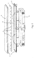
- a lighting device according to the invention according to the Fig. 1 and 2 has as essential functional components a circuit substrate 1 with a plurality of fixed thereto light sources 2, a first housing shell 3 with a contact surface 4 for the circuit substrate 1, a trained like a lens cover second housing shell 5 and a not shown electrical ballast for Driving the light sources 2 and a ballast housing 6.
- the ballast housing 6 which has a trough-shaped design, for example, and has an opening facing the first housing shell, the ballast, not shown, is provided, for example, cast.
- support elements are formed on a side facing away from the contact surface 4, which serve to apply the first housing shell 3 to the ballast housing 6 and to position relative to the same.
- the first housing shell 3 and the ballast housing 6 are firmly bonded together.
- the lighting device according to the invention provides, for example, a plurality of high-power LEDs as light sources 2.
- the lighting device can be designed, for example, in the manner of an outdoor light or in the manner of an industrial light.
- a plurality of positioning means 7 is provided on the first housing shell 3, cf. Fig. 3 ,
- the positioning means 7 are designed in the manner of positioning pins 7. They protrude from the flat contact surface substantially perpendicular.
- the contact surface 4 surrounds a circumferential abutment section 8, which serves to connect the first housing shell 3 to the second housing shell 5.
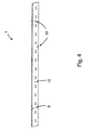
- the circuit substrate 1 is formed in the manner of a circuit board. On the circuit substrate 1 through openings 9,10 are provided. The passage openings 9,10 are provided corresponding to the positioning pins 7 of the first housing shell 3. In particular, the circuit carrier 1 is placed in the contact surface 4 of the first housing shell 3 such that the positioning pins 7 are guided through the passage openings 9, 10.
- a first passage opening 9 is circular in cross-section. A bore diameter of the first passage opening 9 is matched to an outer dimension of the positioning pins 7 such that the associated positioning pin 7 is inserted into the passage opening 9 substantially without play.
- the further passage openings 10 are in the manner of oblong holes educated. The positioning pins 7 are guided in the further passage openings 10 with play. This ensures that the circuit carrier 1 can expand due to thermal stress.
- the second housing shell 5 is formed in the manner of a cover plate. Through the second housing shell 5, the light of the light sources 2 is emitted. As Fig. 5 shows, a web-shaped connecting portion 11 is formed on the second housing shell 5 at the edge, which is dimensioned and shaped so that the second housing shell 5 can be attached to the web-shaped connecting portion 11 in the region of the contact portion 8 to the first housing shell 3. In addition, a plurality of contact elements 12 are provided on the second housing shell 5, which protrude substantially perpendicularly from a transparent light passage surface 13 of the second housing shell 5. The contact elements 12 are formed crescent-shaped or web-like. A free, the light passage surface 13 facing away from the end face of the contact elements 12 tapers in a wedge shape.
- contact elements 12 are arranged distributed in the region of the light passage area 13. In each case, two contact elements 12 are associated with each other in pairs, so that distributed in the region of the light passage surface 13 find four pairs of contact elements.
- the contact element pairs are provided corresponding to the positioning pins 7 of the first housing shell 3 and the passage openings 9, 10 of the circuit substrate 1.
- the Fig. 6 to 8 show the various steps in the manufacture of the lighting device or for connecting the first housing shell 3 with the second housing shell 5.
- the second housing shell 5 is applied with the connecting portion 11 to the abutment portion 8 of the first housing shell 3.
- Two pairs of contact elements 12 associated with each other are provided laterally adjacent to the positioning pin 7.
- the circuit carrier 1 is applied flat to the contact surface 4 of the first housing shell 3.
- the positioning pin 7 is guided by a corresponding passage opening 9 and provided between the contact elements 12.
- an end face 14 of the contact elements 12 is provided at a distance from the circuit carrier 1.
- a contact between the end face 14 and one of the end face 14 facing flat side 15 of the circuit substrate 1 is not formed.
- the positioning pin 7 is provided at a distance from the second housing shell 5. If now an ultrasonic vibration is impressed and the first housing shell 3 pressed against the second housing shell 5, the second housing shell 5 melts in the region of the connecting portion 11 and connect the housing shells 3, 5 in the region of the connecting portion 11 positively.
- Fig. 7 shows an intermediate stage of the joining process.
- the representation after Fig. 7 is selected so that a connection of the first housing shell 3 is formed with the second housing shell 5 in the region of the connecting portion 11 and the wedge-shaped end face 14 for the first time with the flat side 15 of the circuit substrate 1 in contact.
- a contact between an end face 16 of the positioning pin 7 forms with the second housing shell 5.
- the second housing shell 5 is further melted in the region of the connecting portion 11.
- the contact elements 12 melt in the region of the end face 14 and lie flat against the flat side 15 of the circuit substrate 1, compare Fig. 8 .
- the first housing shell 3 and the second housing shell 5 are insofar as, for example, each made of a same material, wherein the respective material pairing materially connects in the respective process management.
- the material of the circuit substrate 1 is selected so that the end faces 14 of the contact elements 12 melt as a result of the vibration vibration, without entering into a material connection with the circuit substrate 1.
- the circuit carrier 1 may be designed to be coated. Nevertheless, the at least wedge-shaped end face 14 of the contact elements 12 is leveled so that the contact elements 12 define the circuit carrier 1 in the area of the end face 14 flat against the contact surface 4.
- a lateral distance 17 between the contact elements 12 and the positioning pin 7 is preferably smaller than 1 cm according to the invention.
- the lateral distance 17 is preferably 0.5 cm or less.
- the distance 17 is presently 1.5 mm.
- a distance dimension 18 between the end face 14 of the contact elements 12 and the flat side 15 of the circuit carrier 1 is preferably 0.4 mm or less, for example, before the first housing shell 3 is connected to the second housing shell 5.
Landscapes
- Engineering & Computer Science (AREA)
- General Engineering & Computer Science (AREA)
- Arrangement Of Elements, Cooling, Sealing, Or The Like Of Lighting Devices (AREA)
Abstract
Description
- Die Erfindung betrifft eine Beleuchtungsvorrichtung mit einem mehrteiligen Gehäuse, mit wenigstens einer Lichtquelle und mit einem die wenigstens eine Lichtquelle tragenden Schaltungsträger, welcher zusammen mit der wenigstens einen Lichtquelle von dem Gehäuse umschlossen ist, wobei das Gehäuse eine erste Gehäuseschale vorsieht, an die der Schaltungsträger angelegt ist und an der mindestens ein Positioniermittel vorgesehen ist, über das der Schaltungsträger relativ zu der ersten Gehäuseschale positioniert ist, wobei das Gehäuse eine zweite Gehäuseschale vorsieht, welche randseitig jedenfalls abschnittsweise einen der ersten Gehäuseschale zugewandten stegförmigen Verbindungsabschnitt aufweist, und wobei die erste Gehäuseschale und die zweite Gehäuseschale im Bereich des stegförmigen Verbindungsbereichs bevorzugt stoffschlüssig miteinander verbunden sind.
- Ferner betrifft die Erfindung ein Herstellungsverfahren für eine Beleuchtungsvorrichtung, eine Gehäuseschale für eine Beleuchtungsvorrichtung sowie die Verwendung der Gehäuseschale für eine erfindungsgemäße Beleuchtungsvorrichtung.
- Im Bereich der Beleuchtungsvorrichtungen ist allgemein bekannt, ein mehrteiliges Gehäuse mit wenigstens zwei Gehäuseschalen vorzusehen, wobei die Gehäuseschalen im Zuge der Montage der Beleuchtungsvorrichtung mittels Vibrationsschweißens stoffschlüssig verbunden werden. Insbesondere wird ein Gehäuse im Bereich der Schweißnaht dicht ausgebildet, sodass einem Eintrag von Feuchtigkeit beziehungsweise Staub vorgebeugt wird. Ebenfalls ist bekannt, einen Schaltungsträger für wenigstens eine Lichtquelle der Beleuchtungsvorrichtung an einer Gehäuseschale festzulegen und über Positioniermittel, insbesondere Positionierstifte, zu positionieren. Eine Festlegung des Schaltungsträgers an der Gehäuseschale erfolgt hierbei üblicherweise mittels Verschrauben, Verklipsen, Verkleben oder dergleichen.
- Aufgabe der vorliegenden Erfindung ist es, eine Beleuchtungsvorrichtung konstruktiv besonders einfach auszubilden und die Herstellung einer Beleuchtungsvorrichtung zu vereinfachen.
- Zur Lösung der Aufgabe ist die Erfindung in Verbindung mit dem Oberbegriff des Patentanspruchs 1 dadurch gekennzeichnet, dass an der zweiten Gehäuseschale mindestens ein Kontaktelement vorgesehen ist, welches derart angeordnet und dimensioniert ist, dass mittels des Kontaktelements der Schaltungsträger mit der wenigstens einen Lichtquelle gegen die zweite Gehäuseschale gedrückt wird.
- Der besondere Vorteil der Erfindung besteht darin, dass durch das Vorsehen des wenigstens einen Kontaktelements an der zweiten Gehäuseschale eine Festlegung des Schaltungsträgers an der ersten Gehäuseschale bewirkt wird und demzufolge auf separate Befestigungsmittel für den Schaltungsträger, beispielsweise Schrauben oder Klebstoff, verzichtet werden kann. Die Beleuchtungsvorrichtung kann demzufolge konstruktiv besonders einfach ausgeführt werden. Darüber hinaus vereinfacht sich die Montage, da beim Verbinden der Gehäuseschalen zugleich auch der Schaltungsträger festgelegt ist.
- Insbesondere kann nach der Erfindung vorgesehen sein, dass an der ersten Gehäuseschale eine Mehrzahl von Positioniermitteln vorgesehen ist, welche nach Art von Positionierstiften ausgebildet sind. Korrespondierend zur Anzahl und Lage der Positionierstifte können an dem Schaltungsträger Durchlassöffnungen vorgesehen sein, welche zur Durchführung beziehungsweise Aufnahme der Positionierstifte vorgesehen sind. Insofern folgt die Positionierung des Schaltungsträgers an der ersten Gehäuseschale in an sich bekannter Weise. Beispielsweise wird eine erste Durchlassöffnung an dem Schaltungsträger nach Art einer Bohrung ausgebildet mit einem im Wesentlichen kreisförmigen Querschnitt. Weitere Durchlassöffnungen können nach Art von Langlöchern ausgebildet sein, sodass die Positionierstifte in den weiteren Durchlassöffnungen spielbehaftet geführt sind und der Schaltungsträger sich thermisch ausdehnen kann. Insbesondere erstrecken sich die langlochförmigen weiteren Durchlass-Öffnungen in eine Längsrichtung der Beleuchtungsvorrichtung, da eine Wärmeausdehnung des Schaltungsträgers in seine Längsrichtung besonders groß ist.
- Nach einer bevorzugten Ausführungsform der Erfindung ist vorgesehen, dass das mindestens eine an der zweiten Gehäuseschale vorgesehene Kontaktelement benachbart zu dem Positioniermittel der ersten Gehäuseschale vorgesehen ist. Vorteilhaft wird der Schaltungsträger demzufolge im Bereich des Positioniermittels festgelegt. Montagetoleranzen werden hierdurch reduziert und eine korrekte Positionierung der optisch wirksamen Funktionskomponenten zueinander gewährleistet. Insbesondere kann vorgesehen sein, dass ein seitlicher Abstand des Positioniermittels zu dem Kontaktelement weniger als 1 cm, bevorzugt weniger als 0,5 cm und besonders bevorzugt 2 mm oder weniger beträgt.
- Nach einer Weiterbildung der Erfindung sind dem Positioniermittel seitlich benachbart wenigstens zwei Kontaktelemente zugeordnet, welche insbesondere paarweise angeordnet sind. Das Positioniermittel kann hierbei zwischen den einander paarweise zugeordneten Kontaktelementen vorgesehen sein. Vorteilhaft ergibt sich durch das paarweise Vorsehen der Kontaktelemente eine gleichmäßige Festlegung des Schaltungsträgers an der ersten Gehäuseschale. Einer schädlichen Verspannung beziehungsweise Biegung des Schaltungsträgers ist damit weitgehend vorgebeugt.
- Zur Lösung der Aufgabe weist ein erfindungsgemäßes Herstellungsverfahren für eine Beleuchtungsvorrichtung die Merkmale des Patentanspruchs 7 auf.
- Der besondere Vorteil des erfindungsgemäßen Verfahrens besteht darin, dass im Zuge des ohnehin vorzusehenden Verbindens der Gehäuseschalen mittels Vibrationsschweißens zugleich der Schaltungsträger von dem wenigstens einen Kontaktelement festgelegt wird. Das Kontaktelement kann insbesondere an einer beliebigen der beiden Gehäuseschalen vorgesehen sein, wobei der Schaltungsträger dann gegen die andere Gehäuseschale angedrückt wird.
- Die Verbindung zwischen der ersten Gehäuseschale und der zweiten Gehäuseschale wird insbesondere im Bereich eines bevorzugt stegförmig ausgebildeten Verbindungsabschnitts hergestellt. Der Verbindungsabschnitt ist beispielsweise umlaufend realisiert, sodass die erste Gehäuseschale am gesamten Umfang mit der zweiten Gehäuseschale verschweißt wird.
- Beispielsweise kann das wenigstens eine Kontaktelement an der zweiten Gehäuseschale vorgesehen sein, wobei an der ersten Gehäuseschale eine Anlagefläche für den Schaltungsträger vorgesehen ist und der Schaltungsträger von dem Kontaktelement gegen die Anlagefläche der ersten Gehäuseschale gedrückt wird. Eine Positionierung des Schaltungsträgers zur ersten Gehäuseschale erfolgt insbesondere über geeignete Positioniermittel, beispielsweise über an der ersten Gehäuseschale vorgesehene Positionierstifte und korrespondierende, an dem Schaltungsträger vorgesehene Durchlassöffnungen für die Positionierstifte.
- Nach einer Weiterbildung der Erfindung kann insbesondere vorgesehen sein, dass das wenigstens eine Kontaktelement infolge des Vibrationsschweißprozesses beim Kontakt mit dem Schaltungsträger an einer dem Schaltungsträger zugewandten Stirnseite aufschmilzt und sich während des Vibrationsschweißens eine Dickenabmessung des Kontaktelements reduziert. Das aufgeschmolzene Kontaktelement legt sich flächig an den Schaltungsträger an. Vorteilhaft ergibt sich hierdurch eine besonders gute und zuverlässige Festlegung des Schaltungsträgers mithilfe des Kontaktelements. Der flächige Kontakt stellt sicher, dass keine zulässig hohen Flächenpressungen auftauchen. Zugleich können Unebenheiten und Fertigungstoleranzen insbesondere aufseiten des Kontaktelements ausgeglichen und eine stets reproduzierbare Festlegung des Schaltungsträgers erreicht werden.
- Die Materialpaarung zwischen dem Kontaktelement einerseits und dem Schaltungsträger andererseits kann insbesondere so gewählt werden, dass das Kontaktelement während des Vibrationsschweißens aufschmilzt und dass es gleichwohl nicht zu einer stoffschlüssigen Verbindung des Kontaktelements mit dem Schaltungsträger kommt. Beispielsweise kann der Schaltungsträger beschichtet ausgebildet sein, um einer stoffschlüssigen Verbindung mit dem Kontaktelement entgegenzuwirken. Insofern ist gewährleistet, dass der Schaltungsträger auch nach dem Verbinden der Gehäuseschalen sich thermisch ausdehnen kann und relativ beweglich zu den Kontaktelementen festgelegt wird.
- Nach einer Weiterbildung der Erfindung ist der Vibrationsschweißprozess insbesondere zweistufig ausgebildet. In einem ersten Prozessschritt wird die zweite Gehäuseschale im Bereich des Verbindungsabschnitts aufgeschmolzen und mit der ersten Gehäuseschale stoffschlüssig verbunden. Das Kontaktelement nähert sich hierbei dem Schaltungsträger an. Sobald das Kontaktelement den Schaltungsträger berührt und diesen gegen die erste Gehäuseschale gedrückt hat, wird in einem zweiten Prozessschritt das Kontaktelement im Bereich der dem Schaltungsträger zugewandten Stirnseite infolge der Vibrationsschwingungen aufgeschmolzen. Zugleich wird die Verschweißung der zweiten Gehäuseschale mit der ersten Gehäuseschale während des zweiten Prozessschritts fortgesetzt. Vorteilhaft bewirkt die Zweistufigkeit des Prozesses, dass zunächst die Gehäuseschalen miteinander verbunden und einander angenähert werden. Der Schaltungsträger wird dabei sukzessive an die erste Gehäuseschale angenähert und positioniert. Sobald der Schaltungsträger an der ersten Gehäuseschale anliegt und das Kontaktelement den Schaltungsträger berührt, wird dieser festgelegt. Die Zweistufigkeit begünstigt demzufolge die exakte Positionierung des Schaltungsträgers an der ersten Gehäuseschale.
- Nach einer Weiterbildung der Erfindung ist vorgesehen, dass die Gehäuseschalen bei einer Frequenz von 240 Hz oder mehr vibrationsverschweißt werden. Es handelt sich hierbei um ein im industriellen Umfeld lange erprobtes Verfahren, welches prozessseitig gut beherrschbar ist und zu einer zuverlässigen und dauerhaften stoffschlüssigen Verbindung der Gehäuseschalen führt. Insbesondere werden beim Vibrationsverschweißen Schwingweiten von 0,8 bis 1,8 mm aufgeprägt.
- Zur Lösung der Aufgabe weist eine erfindungsgemäße Gehäuseschale die Merkmale des Patentanspruchs 11 auf.
- Eine erfindungsgemäße Gehäuseschale weist insbesondere randseitig einen stegförmigen Verbindungsabschnitt und einen in Richtung des stegförmigen Verbindungsabschnitts orientiertes Kontaktelement auf. Im Bereich einer freien Stirnseite desselben ist an dem Kontaktelement ein sich verjüngender Querschnitt ausgebildet. Beispielsweise verjüngt sich das Kontaktelement im Bereich der freien Stirnseite nach Art einer Spitze oder keilförmig. Vorteilhaft begünstigt die sich verjüngende Stirnseite das Aufschmelzen des Kontaktelements im Bereich derselben infolge der Vibrationsschwingung. Es ist zunächst relativ wenig Material in direktem Kontakt mit dem Schaltungsträger, sodass sich innerhalb kurzer Zeit eine Schmelze ausbildet und die verjüngende Stirnseite sich flächig an dem Schaltungsträger anlegt.
- Indem die freie Stirnseite des Kontaktelements in Bezug zu einer freien Stirnfläche des stegförmigen Verbindungsabschnitts zurückversetzt angeordnet ist, kann die Zweistufigkeit des Herstellungsprozesses konstruktiv begünstigt werden. Infolge der zurückversetzten Anordnung des Kontaktelements kommt es zunächst zum Kontakt der freien Stirnseite des Verbindungsabschnitts mit der ersten Gehäuseschale. Erst durch das Aufprägen von Vibrationsschwingungen, das Aufschmelzen des stegförmigen Verbindungsabschnitts und die Verbindung der Gehäuseschalen nähert sich das Kontaktelement dem Schaltungsträger an. Der Zeitpunkt der Berührung des Kontaktelements und des Schaltungsträgers kann somit konstruktiv vorbestimmt beziehungsweise beeinflusst werden.
- Aus den weiteren Unteransprüchen und der nachfolgenden Beschreibung sind weitere Vorteile, Merkmale und Einzelheiten der Erfindung zu entnehmen. Dort erwähnte Merkmale können jeweils einzeln für sich oder auch in beliebiger Kombination erfindungswesentlich sein. Erfindungsgemäß beschriebene Merkmale und Details der Beleuchtungsvorrichtung gelten selbstverständlich auch im Zusammenhang mit dem erfindungsgemäßen Herstellungsverfahren sowie und umgekehrt. Gleiches gilt für die Verwendung einer Gehäuseschale für die erfindungsgemäße Beleuchtungsvorrichtung. So kann auf die Offenbarung zu den einzelnen Erfindungsaspekten stets wechselseitig Bezug genommen werden. Die Zeichnungen dienen lediglich beispielhaft der Klarstellung der Erfindung und haben keinen einschränkenden Charakter.
- Anhand der beigefügten Zeichnungen wird die Erfindung nachfolgend näher erläutert. Dabei zeigt:
- Fig. 1
- eine perspektivische Seitenansicht einer erfindungsgemäßen Beleuchtungsvorrichtung,
- Fig. 2
- eine Explosionsdarstellung einzelner Komponenten der Beleuchtungsvorrichtung nach
Fig. 1 , - Fig. 3
- eine Detailansicht einer ersten Gehäuseschale der Beleuchtungsvorrichtung nach
Fig. 1 , - Fig. 4
- eine Detailansicht eines Schaltungsträgers der Beleuchtungsvorrichtung nach
Fig. 1 , - Fig. 5
- eine zweite Gehäuseschale der Beleuchtungsvorrichtung nach
Fig. 1 , - Fig. 6
- einen ersten Verfahrensschritt beim Verbinden der ersten Gehäuseschale mit der zweiten Gehäuseschale,
- Fig. 7
- einen zweiten Verfahrensschritt beim Verbinden der ersten Gehäuseschale mit der zweiten Gehäuseschale und
- Fig. 8
- einen dritten Verfahrensschritt beim Verbinden der ersten Gehäuseschale mit der zweiten Gehäuseschale.
- Eine erfindungsgemäße Beleuchtungsvorrichtung nach den
Fig. 1 und2 weist als wesentliche Funktionskomponenten einen Schaltungsträger 1 mit einer Mehrzahl von daran festgelegten Lichtquellen 2, eine erste Gehäuseschale 3 mit einer Anlagefläche 4 für den Schaltungsträger 1, eine nach Art einer Abschlussscheibe ausgebildete zweite Gehäuseschale 5 sowie ein nicht dargestelltes elektrisches Vorschaltgerät zum Ansteuern der Lichtquellen 2 und ein Vorschaltgehäuse 6 auf. In dem Vorschaltgehäuse 6, welches beispielsweise wannenförmig ausgebildet und eine der ersten Gehäuseschale zugewandte Öffnung aufweist, ist das nicht dargestellte Vorschaltgerät beispielsweise vergossen vorgesehen. Als Teil der ersten Gehäuseschale 3 sind auf einer der Anlagefläche 4 abgewandten Seite Trägerelemente ausgebildet, welche dazu dienen, die erste Gehäuseschale 3 an das Vorschaltgehäuse 6 anzulegen und relativ zu demselben zu positionieren. Beispielsweise werden die erste Gehäuseschale 3 und das Vorschaltgehäuse 6 stoffschlüssig miteinander verbunden. - Die erfindungsgemäße Beleuchtungsvorrichtung sieht als Lichtquellen 2 beispielsweise eine Mehrzahl von Hochleistungs-LED vor. Die Beleuchtungsvorrichtung kann beispielsweise nach Art einer Außenleuchte oder nach Art einer Industrieleuchte ausgebildet sein.
- Im Bereich der Anlagefläche 4 ist an der ersten Gehäuseschale 3 eine Mehrzahl von Positioniermitteln 7 vorgesehen, vergleiche.
Fig. 3 . Die Positioniermittel 7 sind nach Art von Positionierstiften 7 ausgebildet. Sie ragen von der ebenen Anlagefläche im Wesentlichen senkrecht ab. Randseitig umgibt die Anlagefläche 4 ein umlaufender Anlageabschnitt 8, welcher dazu dient, die erste Gehäuseschale 3 mit der zweiten Gehäuseschale 5 zu verbinden. - An die Anlagefläche 4 der ersten Gehäuseschale 3 wird der Schaltungsträger 1 angelegt. Wie insbesondere
Fig. 4 zeigt, ist der Schaltungsträger 1 nach Art einer Platine ausgebildet. An dem Schaltungsträger 1 sind Durchlassöffnungen 9,10 vorgesehen. Die Durchlassöffnungen 9,10 sind korrespondierend zu den Positionierstiften 7 der ersten Gehäuseschale 3 vorgesehen. Insbesondere wird der Schaltungsträger 1 so in die Anlagefläche 4 der ersten Gehäuseschale 3 angelegt, dass die Positionierstifte 7 durch die Durchlassöffnungen 9,10 geführt sind. Eine erste Durchlassöffnung 9 ist im Querschnitt kreisförmig ausgebildet. Ein Bohrungsdurchmesser der ersten Durchlassöffnung 9 ist so auf eine Außenabmessung der Positionierstifte 7 abgestimmt, dass der zugeordnete Positionierstift 7 im Wesentlichen spielfrei in die Durchlassöffnung 9 eingesetzt wird. Die weiteren Durchlassöffnungen 10 sind nach Art von Langlöchern ausgebildet. Die Positionierstifte 7 werden in den weiteren Durchlassöffnungen 10 spielbehaftet geführt. Hierdurch ist gewährleistet, dass sich der Schaltungsträger 1 infolge einer thermischen Belastung ausdehnen kann. - Die zweite Gehäuseschale 5 ist nach Art einer Abschlussscheibe ausgebildet. Durch die zweite Gehäuseschale 5 wird das Licht der Lichtquellen 2 abgestrahlt. Wie
Fig. 5 zeigt, ist an der zweiten Gehäuseschale 5 randseitig ein stegförmiger Verbindungsabschnitt 11 ausgebildet, welcher so dimensioniert und geformt ist, dass die zweite Gehäuseschale 5 mit dem stegförmigen Verbindungsabschnitt 11 im Bereich des Anlageabschnitts 8 an die erste Gehäuseschale 3 angesetzt werden kann. Zusätzlich ist an der zweiten Gehäuseschale 5 eine Mehrzahl von Kontaktelementen 12 vorgesehen, welche im Wesentlichen senkrecht von einer transparenten Lichtdurchtrittsfläche 13 der zweiten Gehäuseschale 5 abragen. Die Kontaktelemente 12 sind halbmondförmig beziehungsweise stegartig ausgebildet. Eine freie, der Lichtdurchtrittsfläche 13 abgewandte Stirnseite der Kontaktelemente 12 verjüngt sich keilförmig. - Insgesamt sind acht Kontaktelemente 12 im Bereich der Lichtdurchtrittsfläche 13 verteilt angeordnet. Jeweils zwei Kontaktelemente 12 sind einander paarweise zugeordnet, sodass sich im Bereich der Lichtdurchtrittsfläche 13 verteilt vier Kontaktelementpaare finden. Die Kontaktelementpaare sind korrespondierend zu den Positionierstiften 7 der ersten Gehäuseschale 3 und den Durchlassöffnungen 9, 10 des Schaltungsträgers 1 vorgesehen.
- Die
Fig. 6 bis 8 zeigen die verschiedenen Schritte bei der Herstellung der Beleuchtungsvorrichtung beziehungsweise zum Verbinden der ersten Gehäuseschale 3 mit der zweiten Gehäuseschale 5. In einer Ausgangsposition wird die zweite Gehäuseschale 5 mit dem Verbindungsabschnitt 11 an den Anlageabschnitt 8 der ersten Gehäuseschale 3 angelegt. Zwei einander paarweise zugeordneten Kontaktelemente 12 sind seitlich benachbart zu dem Positionierstift 7 vorgesehen. Der Schaltungsträger 1 ist flächig an die Anlagefläche 4 der ersten Gehäuseschale 3 angelegt. Der Positionierstift 7 ist dabei durch eine korrespondierende Durchlassöffnung 9 geführt und zwischen den Kontaktelementen 12 vorgesehen. - In der Ausgangskonfiguration ist eine Stirnseite 14 der Kontaktelemente 12 beabstandet zu dem Schaltungsträger 1 vorgesehen. Ein Kontakt zwischen der Stirnseite 14 und einer der Stirnseite 14 zugewandten Flachseite 15 des Schaltungsträgers 1 ist nicht ausgebildet. Ebenso ist der Positionierstift 7 beabstandet von der zweiten Gehäuseschale 5 vorgesehen. Wird nunmehr eine Ultraschallschwingung aufgeprägt und die erste Gehäuseschale 3 gegen die zweite Gehäuseschale 5 gedrückt, schmilzt die zweite Gehäuseschale 5 im Bereich des Verbindungsabschnitts 11 auf und es verbinden sich die Gehäuseschalen 3, 5 im Bereich des Verbindungsabschnitts 11 formschlüssig.
-
Fig. 7 zeigt eine Zwischenstufe des Fügeprozesses. Die Darstellung nachFig. 7 ist so gewählt, dass eine Verbindung der ersten Gehäuseschale 3 mit der zweiten Gehäuseschale 5 im Bereich des Verbindungsabschnitts 11 ausgebildet ist und die keilförmige Stirnseite 14 erstmalig mit der Flachseite 15 des Schaltungsträgers 1 in Kontakt tritt. Zeitgleich bildet sich ein Kontakt zwischen einer Stirnfläche 16 des Positionierstifts 7 mit der zweiten Gehäuseschale 5 aus. - Wird das Gehäuse 3, 5 unverändert zu Vibrationsschwingungen angeregt und die Gehäuseschale 3 gegen die zweite Gehäuseschale 5 gedrückt, wird die zweite Gehäuseschale 5 im Bereich des Verbindungsabschnitts 11 weiter aufgeschmolzen. Zudem schmelzen die Kontaktelemente 12 im Bereich der Stirnseite 14 auf und legen sich flächig an die Flachseite 15 des Schaltungsträgers 1 an, vergleiche
Fig. 8 . Ebenso schmilzt die Stirnfläche 16 des Positionierstifts 7. Infolge der Materialwahl kommt es zu einer schlüssigen Verbindung im Bereich des Verbindungsabschnitts 11 und des Anlageabschnitts 8 einerseits und im Bereich der Stirnfläche 16 mit der zweiten Gehäuseschale 5. Die erste Gehäuseschale 3 und die zweite Gehäuseschale 5 sind insofern beispielsweise jeweils für sich aus einem gleichen Werkstoff hergestellt, wobei sich die jeweilige Werkstoffpaarung bei der jeweiligen Prozessführung stoffschlüssig verbindet. - Insbesondere zwischen dem Schaltungsträger 1 und der Stirnseite 14 der Kontaktelemente 12 kommt es vorliegend nicht zu einer stoffschlüssigen Verbindung. Beispielsweise ist das Material des Schaltungsträgers 1 so gewählt, dass die Stirnseiten 14 der Kontaktelemente 12 infolge der Vibrationsschwingung aufschmelzen, ohne eine stoffschlüssige Verbindung mit dem Schaltungsträger 1 einzugehen. Beispielsweise kann der Schaltungsträger 1 beschichtet ausgeführt sein. Gleichwohl wird die zumindest keilförmige Stirnseite 14 der Kontaktelemente 12 eingeebnet, sodass die Kontaktelemente 12 den Schaltungsträger 1 im Bereich der Stirnseite 14 flächig gegen die Anlagefläche 4 festlegen.
- Ein seitlicher Abstand 17 zwischen den Kontaktelementen 12 und dem Positionierstift 7 ist nach der Erfindung bevorzugt kleiner als 1 cm. Der seitliche Abstand 17 beträgt bevorzugt 0,5 cm oder weniger. Der Abstand 17 beträgt vorliegend 1,5 mm. Ein Abstandsmaß 18 zwischen der Stirnseite 14 der Kontaktelemente 12 und der Flachseite 15 des Schaltungsträgers 1 ist vor dem Verbinden der ersten Gehäuseschale 3 mit der zweiten Gehäuseschale 5 beispielsweise bevorzugt 0,4 mm oder weniger.
-
- 1
- Schaltungsträger
- 2
- Lichtquelle
- 3
- erste Gehäuseschale
- 4
- Anlagefläche
- 5
- zweite Gehäuseschale
- 6
- Vorschaltgehäuse
- 7
- Positioniermittel
- 8
- Anlageabschnitt
- 9
- Durchlassöffnung
- 10
- Durchlassöffnung
- 11
- Verbindungsabschnitt
- 12
- Kontaktelement
- 13
- Lichtdurchtrittsfläche
- 14
- Stirnseite
- 15
- Flachseite
- 16
- Stirnfläche
- 17
- seitlicher Abstand
- 18
- Abstandsmaß
Claims (15)
- Beleuchtungsvorrichtung mit einem mehrteiligen Gehäuse, mit wenigstens einer Lichtquelle (2) und mit einem die wenigstens eine Lichtquelle (2) tragenden Schaltungsträger (1), welcher zusammen mit der wenigstens einen Lichtquelle (2) von dem Gehäuse umschlossen ist, wobei das Gehäuse eine erste Gehäuseschale (3) vorsieht, an die der Schaltungsträger (1) angelegt ist und an der mindestens ein Positioniermittel (7) vorgesehen ist, über das der Schaltungsträger (1) relativ zu der ersten Gehäuseschale (3) positioniert ist, wobei das Gehäuse eine zweite Gehäuseschale (5) vorsieht, welche randseitig jedenfalls abschnittsweise einen der ersten Gehäuseschale (3) zugewandten stegförmigen Verbindungsabschnitt (11) aufweist, und wobei die erste Gehäuseschale (3) und die zweite Gehäuseschale (5) im Bereich des stegförmigen Verbindungsbereichs bevorzugt stoffschlüssig miteinander verbunden sind, dadurch gekennzeichnet, dass an der zweiten Gehäuseschale (5) mindestens ein Kontaktelement (12) vorgesehen ist, welches derart angeordnet und dimensioniert ist, dass mittels des Kontaktelements (12) der Schaltungsträger (1) mit der wenigstens einen Lichtquelle (2) gegen die erste Gehäuseschale (3) gedrückt wird.
- Beleuchtungsvorrichtung nach Anspruch 1, dadurch gekennzeichnet, dass das mindestens eine an der zweiten Gehäuseschale (5) vorgesehene Kontaktelement (12) benachbart zu dem Positioniermittel (7) der ersten Gehäuseschale (3) vorgesehen ist.
- Beleuchtungsvorrichtung nach Anspruch 1 oder 2, dadurch gekennzeichnet, dass ein seitlicher Abstand (17) des Positioniermittels (7) zu dem Kontaktelement (12) weniger als 1 cm, bevorzugt weniger als 0,5 cm beträgt.
- Beleuchtungsvorrichtung nach einem der Ansprüche 1 bis 3, dadurch gekennzeichnet, dass dem Positioniermittel (7) seitlich benachbart paarweise zwei Kontaktelemente (12) zugeordnet sind, wobei das Positioniermittel (7) zwischen den zwei einander paarweise zugeordneten Kontaktelementen (12) vorgesehen ist.
- Beleuchtungsvorrichtung nach einem der Ansprüche 1 bis 4, dadurch gekennzeichnet, dass das an der ersten Gehäuseschale (3) vorgesehene Positioniermittel (7) nach Art eines Positionierstifts (7) ausgebildet ist und dass an dem Schaltungsträger (1) eine Durchlassöffnung (9, 10) vorgesehen ist zum Aufnehmen des Positionierstifts (7).
- Beleuchtungsvorrichtung nach einem der Ansprüche 1 bis 5, dadurch gekennzeichnet, dass an der ersten Gehäuseschale (3) eine Mehrzahl von Positionierstiften (7) vorgesehen ist und dass an dem Schaltungsträger (1) eine Mehrzahl von Durchlassöffnungen (9,10) ausgebildet ist, wobei eine erste Durchlassöffnung (9) nach Art einer Bohrung ausgebildet ist mit einem Bohrungsdurchmesser, welcher auf die Dimension eines zugeordneten Positionierstifts (7) abgestimmt ist, und wobei weitere Durchlassöffnungen (10) nach Art von Langlöchern ausgebildet sind derart, dass die weiteren Positioniermittel (7) der ersten Gehäuseschale (3) spielbehaftet in den weiteren Durchlassöffnungen (10) vorgesehen sind.
- Herstellungsverfahren für eine Beleuchtungsvorrichtung, insbesondere für eine Beleuchtungsvorrichtung nach einem der Ansprüche 1 bis 6, wobei eine erste Gehäuseschale (3) mit einer zweiten Gehäuseschale (5) mittels Vibrationsschweißens verbunden wird und wobei ein Schaltungsträger (1) der Beleuchtungsvorrichtung mit wenigstens einer hieran festgelegten Lichtquelle (2) zwischen der ersten Gehäuseschale (3) und der zweiten Gehäuseschale (5) festgelegt wird, indem- die zweite Gehäuseschale (5) mit einem bevorzugt stegförmigen Verbindungsabschnitt (11) an die erste Gehäuseschale (3) angelegt wird;- Vibrationsschwingungen aufgeprägt werden und die erste Gehäuseschale (3) gegen die zweite Gehäuseschale (5) gedrückt wird, wodurch sich die zweite Gehäuseschale (5) im Bereich des Verbindungsabschnitts (11) mit der ersten Gehäuseschale (3) verbindet und eine Dickenabmessung des Verbindungsabschnitts (11) sich reduziert;- der Schaltungsträger (1) durch ein an der zweiten Gehäuseschale (5) vorgesehenes Kontaktelement (12) an die andere Gehäuseschale (3) angedrückt wird.
- Verfahren nach Anspruch 7, dadurch gekennzeichnet, dass das Kontaktelement (12) während des Vibrationsschweißens aufgeschmolzen wird und/oder dass eine Dickenabmessung des Kontaktelements (12) während des Vibrationsschweißens abnimmt und/oder dass sich das Kontaktelement (12) mit einer dem Schaltungsträger (1) zugewandten Stirnseite (14) flächig an diesen anlegt.
- Verfahren nach Anspruch 7 oder 8, dadurch gekennzeichnet, dass das Vibrationsschweißen in wenigstens zwei Prozessschritten erfolgt,- wobei in einem ersten Prozessschritt die zweite Gehäuseschale (5) im Bereich des Verbindungsabschnitts (11) aufschmilzt und mit der ersten Gehäuseschale (3) stoffschlüssig verbunden wird, während das Kontaktelement (12) beabstandet zu dem Schaltungsträger (1) vorgesehen ist und an den Schaltungsträger (1) angenähert wird, und- wobei in einem zweiten Prozessschritt die erste Gehäuseschale (3) mit der zweiten Gehäuseschale (5) im Bereich des Verbindungsabschnitts (11) fortgesetzt verschweißt wird und zudem das Kontaktelement (12) im Bereich der an dem Schaltungsträger (1) zugewandten Stirnseite (14) infolge der Vibrationsschwingungen und des Kontakts mit dem Schaltungsträger (1) aufschmilzt.
- Verfahren nach einem der Ansprüche 7 bis 9, dadurch gekennzeichnet, dass eine Frequenz für das Vibrationsschweißen 240 Hz oder mehr beträgt.
- Gehäuseschale (5) für eine Beleuchtungsvorrichtung, insbesondere für eine Beleuchtungsvorrichtung nach einem der Ansprüche 1 bis 6, wobei an der Gehäuseschale (5) randseitig ein stegförmiger Verbindungsabschnitt (11) jedenfalls abschnittsweise vorgesehen ist und wobei von der Gehäuseschale (5) wenigstens ein Kontaktelement (12) abragt, welches im Bereich einer freien Stirnseite (14) desselben einen sich verjüngenden Querschnitt aufweist.
- Gehäuseschale (5) nach Anspruch 11, dadurch gekennzeichnet, dass das Kontaktelement (12) im Bereich der freien Stirnseite (14) sich spitz und/oder keilförmig verjüngt.
- Gehäuseschale (5) nach Anspruch 11 oder 12, dadurch gekennzeichnet, dass eine Stirnseite (14) des Kontaktelements (12) in Bezug zu einer freien Stirnfläche des stegförmigen Verbindungsabschnitts (11) derart zurückversetzt angeordnet ist, dass zunächst ein Kontakt zwischen dem Verbindungsabschnitt (11) und der ersten Gehäuseschale (3) ausgebildet ist, während das Kontaktelement (12) beabstandet zu dem Schaltungsträger (1) vorgesehen ist.
- Gehäuseschale (5) nach einem der Ansprüche 11 bis 13, dadurch gekennzeichnet, dass eine Mehrzahl von Kontaktelementen (12) vorgesehen ist, welche beabstandet zueinander angeordnet sind und/oder einander paarweise zugeordnet sind.
- Verwendung einer Gehäuseschale (5) nach einem der Ansprüche 11 bis 14 als zweite Gehäuseschale (5) einer Beleuchtungsvorrichtung nach einem der Ansprüche 1 bis 6.
Priority Applications (2)
| Application Number | Priority Date | Filing Date | Title |
|---|---|---|---|
| EP14159703.9A EP2918393B1 (de) | 2014-03-14 | 2014-03-14 | Beleuchtungsvorrichtung, Gehäuseschale für eine Beleuchtungsvorrichtung und Herstellungsverfahren für eine Beleuchtungsvorrichtung |
| PCT/EP2015/055377 WO2015136113A1 (de) | 2014-03-14 | 2015-03-14 | Beleuchtungsvorrichtung; gehäuseschale für eine beleuchtungsvorrichtung und herstellungsverfahren für eine beleuchtungsvorrichtung |
Applications Claiming Priority (1)
| Application Number | Priority Date | Filing Date | Title |
|---|---|---|---|
| EP14159703.9A EP2918393B1 (de) | 2014-03-14 | 2014-03-14 | Beleuchtungsvorrichtung, Gehäuseschale für eine Beleuchtungsvorrichtung und Herstellungsverfahren für eine Beleuchtungsvorrichtung |
Publications (2)
| Publication Number | Publication Date |
|---|---|
| EP2918393A1 true EP2918393A1 (de) | 2015-09-16 |
| EP2918393B1 EP2918393B1 (de) | 2021-08-04 |
Family
ID=50277037
Family Applications (1)
| Application Number | Title | Priority Date | Filing Date |
|---|---|---|---|
| EP14159703.9A Active EP2918393B1 (de) | 2014-03-14 | 2014-03-14 | Beleuchtungsvorrichtung, Gehäuseschale für eine Beleuchtungsvorrichtung und Herstellungsverfahren für eine Beleuchtungsvorrichtung |
Country Status (2)
| Country | Link |
|---|---|
| EP (1) | EP2918393B1 (de) |
| WO (1) | WO2015136113A1 (de) |
Cited By (1)
| Publication number | Priority date | Publication date | Assignee | Title |
|---|---|---|---|---|
| EP3477195A1 (de) * | 2017-10-24 | 2019-05-01 | TRILUX GmbH & Co. KG | Langfeldleuchte, insbesondere lichtbandleuchte, sowie daraus aufgebautes lichtband |
Families Citing this family (2)
| Publication number | Priority date | Publication date | Assignee | Title |
|---|---|---|---|---|
| EP4522064B1 (de) * | 2023-07-28 | 2026-06-24 | KaVo Dental GmbH | Medizinische leuchte |
| DE202024100229U1 (de) * | 2024-01-18 | 2025-04-25 | Zumtobel Lighting Gmbh | Leuchtenträgereinheit und damit ausgestattete Leuchte |
Citations (2)
| Publication number | Priority date | Publication date | Assignee | Title |
|---|---|---|---|---|
| EP2306068A1 (de) * | 2008-07-15 | 2011-04-06 | CCS Inc. | Beleuchtungsvorrichtung |
| WO2013007450A1 (en) * | 2011-07-08 | 2013-01-17 | Osram Ag | Light-emitting device |
Family Cites Families (1)
| Publication number | Priority date | Publication date | Assignee | Title |
|---|---|---|---|---|
| DE102011051047B4 (de) * | 2011-06-14 | 2015-06-18 | Hella Kgaa Hueck & Co. | Beleuchtungseinrichtung |
-
2014
- 2014-03-14 EP EP14159703.9A patent/EP2918393B1/de active Active
-
2015
- 2015-03-14 WO PCT/EP2015/055377 patent/WO2015136113A1/de not_active Ceased
Patent Citations (2)
| Publication number | Priority date | Publication date | Assignee | Title |
|---|---|---|---|---|
| EP2306068A1 (de) * | 2008-07-15 | 2011-04-06 | CCS Inc. | Beleuchtungsvorrichtung |
| WO2013007450A1 (en) * | 2011-07-08 | 2013-01-17 | Osram Ag | Light-emitting device |
Cited By (1)
| Publication number | Priority date | Publication date | Assignee | Title |
|---|---|---|---|---|
| EP3477195A1 (de) * | 2017-10-24 | 2019-05-01 | TRILUX GmbH & Co. KG | Langfeldleuchte, insbesondere lichtbandleuchte, sowie daraus aufgebautes lichtband |
Also Published As
| Publication number | Publication date |
|---|---|
| WO2015136113A1 (de) | 2015-09-17 |
| EP2918393B1 (de) | 2021-08-04 |
Similar Documents
| Publication | Publication Date | Title |
|---|---|---|
| DE102012213193B4 (de) | Anordnung von optischen halbleiterelementen | |
| EP3066907A1 (de) | Befestigungselement zur befestigung an einer leiterplatte sowie befestigungsvorrichtung und verfahren zum beabstandeten verbinden von leiterplatten mit einem derartigen befestigungselement | |
| EP3477781A1 (de) | Steckerbuchse für leiterplatinen | |
| EP2918393B1 (de) | Beleuchtungsvorrichtung, Gehäuseschale für eine Beleuchtungsvorrichtung und Herstellungsverfahren für eine Beleuchtungsvorrichtung | |
| EP3492809B1 (de) | Fahrzeugscheinwerfer und verfahren zur justierung einer lichtquelle und einer vorsatzoptik | |
| DE2414790A1 (de) | Kristall-oszillator | |
| DE112021000365B4 (de) | Fluidsteuervorrichtung mit reduzierung des widerstands im strömungspfad durch ventilanordnung | |
| DE102017109159B4 (de) | Ultraschallwandlereinrichtung und Kontaktierungsverfahren | |
| DE102015226636A1 (de) | Leuchtvorrichtung mit laserdiode und wandlereinrichtung | |
| DE102016224666A1 (de) | Verfahren zur Herstellung einer Fügeverbindung sowie eine Fügeverbindung | |
| DE102010063151A1 (de) | Steuergerät und Verfahren zum Herstellen eines Steuergeräts | |
| EP4165455B1 (de) | Mikrolinsenanordnung und mikrooptische vorrichtung | |
| WO2007124994A1 (de) | Optisches modul und verfahren zum herstellen eines optischen moduls | |
| EP4251883B1 (de) | Verdichter | |
| DE202012003185U1 (de) | Schwingvorrichtung für eine Füllstandsmesseinheit | |
| EP2029940B1 (de) | Verfahren zur herstellung eines blendenteils für ein bedienpanel mit berührungsempfindlichen sensortasten, insbesondere für ein haushaltsgerät | |
| DE202016101380U1 (de) | Montageelement aus LED, LED-Anschlusselement und Anschlusskontakt sowie Anschlusselemente zur Herstellung einer solchen Montageeinheit | |
| EP0651504B1 (de) | Halterung für Schwingquarzscheiben | |
| EP2918904B1 (de) | Beleuchtungsvorrichtung und Montageverfahren für eine Beleuchtungseinrichtung | |
| DE102012205168B4 (de) | Schwingvorrichtung für eine Füllstandsmesseinheit sowie Verfahren zur Montage der Schwingvorrichtung | |
| DE10259277A1 (de) | Einspannvorrichtung und Verfahren zur Fixierung von mindestens einem elektronischen Bauteils auf einer Leiterplatte und zum Löten des Bauteils | |
| EP2860554B1 (de) | Verfahren zur Herstellung eines optoelektronischen Sensors | |
| EP3365151A1 (de) | Schweissbaugruppe und verfahren zur herstellung einer schweissbaugruppe | |
| DE102022113252A1 (de) | Lichtmodul mit einer Strahlenblende sowie Verfahren zum lagegenauen Befestigen einer Strahlenblende | |
| DE102024124159A1 (de) | Sonotrode, Vorrichtung und Verfahren zur Ultraschallbearbeitung von Werkstücken |
Legal Events
| Date | Code | Title | Description |
|---|---|---|---|
| PUAI | Public reference made under article 153(3) epc to a published international application that has entered the european phase |
Free format text: ORIGINAL CODE: 0009012 |
|
| AK | Designated contracting states |
Kind code of ref document: A1 Designated state(s): AL AT BE BG CH CY CZ DE DK EE ES FI FR GB GR HR HU IE IS IT LI LT LU LV MC MK MT NL NO PL PT RO RS SE SI SK SM TR |
|
| AX | Request for extension of the european patent |
Extension state: BA ME |
|
| 17P | Request for examination filed |
Effective date: 20151030 |
|
| RBV | Designated contracting states (corrected) |
Designated state(s): AL AT BE BG CH CY CZ DE DK EE ES FI FR GB GR HR HU IE IS IT LI LT LU LV MC MK MT NL NO PL PT RO RS SE SI SK SM TR |
|
| RAP1 | Party data changed (applicant data changed or rights of an application transferred) |
Owner name: HELLA GMBH & CO. KGAA |
|
| RAP1 | Party data changed (applicant data changed or rights of an application transferred) |
Owner name: LUNUX GMBH |
|
| RIC1 | Information provided on ipc code assigned before grant |
Ipc: F21Y 103/00 20160101ALN20141002BHEP Ipc: B29C 65/74 20060101AFI20141002BHEP Ipc: F21V 17/00 20060101ALI20141002BHEP Ipc: F21V 15/01 20060101ALI20141002BHEP Ipc: F21Y 101/02 20181130ALN20141002BHEP Ipc: F21V 19/00 20060101ALI20141002BHEP |
|
| RIC1 | Information provided on ipc code assigned before grant |
Ipc: F21Y 103/00 20160101ALN20141002BHEP Ipc: F21V 15/01 20060101ALI20141002BHEP Ipc: F21Y 101/02 20000101ALN20141002BHEP Ipc: F21V 19/00 20060101ALI20141002BHEP Ipc: F21V 17/00 20060101ALI20141002BHEP Ipc: B29C 65/74 20060101AFI20141002BHEP |
|
| STAA | Information on the status of an ep patent application or granted ep patent |
Free format text: STATUS: EXAMINATION IS IN PROGRESS |
|
| 17Q | First examination report despatched |
Effective date: 20190710 |
|
| REG | Reference to a national code |
Ref country code: DE Ref legal event code: R079 Ref document number: 502014015782 Country of ref document: DE Free format text: PREVIOUS MAIN CLASS: B29C0065740000 Ipc: F21V0015010000 |
|
| GRAP | Despatch of communication of intention to grant a patent |
Free format text: ORIGINAL CODE: EPIDOSNIGR1 |
|
| STAA | Information on the status of an ep patent application or granted ep patent |
Free format text: STATUS: GRANT OF PATENT IS INTENDED |
|
| RIC1 | Information provided on ipc code assigned before grant |
Ipc: F21V 15/01 20060101AFI20210125BHEP |
|
| INTG | Intention to grant announced |
Effective date: 20210218 |
|
| GRAS | Grant fee paid |
Free format text: ORIGINAL CODE: EPIDOSNIGR3 |
|
| GRAA | (expected) grant |
Free format text: ORIGINAL CODE: 0009210 |
|
| STAA | Information on the status of an ep patent application or granted ep patent |
Free format text: STATUS: THE PATENT HAS BEEN GRANTED |
|
| RAP1 | Party data changed (applicant data changed or rights of an application transferred) |
Owner name: LUNUX LIGHTING GMBH |
|
| AK | Designated contracting states |
Kind code of ref document: B1 Designated state(s): AL AT BE BG CH CY CZ DE DK EE ES FI FR GB GR HR HU IE IS IT LI LT LU LV MC MK MT NL NO PL PT RO RS SE SI SK SM TR |
|
| REG | Reference to a national code |
Ref country code: GB Ref legal event code: FG4D Free format text: NOT ENGLISH |
|
| REG | Reference to a national code |
Ref country code: AT Ref legal event code: REF Ref document number: 1417336 Country of ref document: AT Kind code of ref document: T Effective date: 20210815 |
|
| REG | Reference to a national code |
Ref country code: CH Ref legal event code: EP |
|
| REG | Reference to a national code |
Ref country code: DE Ref legal event code: R096 Ref document number: 502014015782 Country of ref document: DE |
|
| REG | Reference to a national code |
Ref country code: IE Ref legal event code: FG4D Free format text: LANGUAGE OF EP DOCUMENT: GERMAN |
|
| REG | Reference to a national code |
Ref country code: NL Ref legal event code: FP |
|
| REG | Reference to a national code |
Ref country code: LT Ref legal event code: MG9D |
|
| PG25 | Lapsed in a contracting state [announced via postgrant information from national office to epo] |
Ref country code: SE Free format text: LAPSE BECAUSE OF FAILURE TO SUBMIT A TRANSLATION OF THE DESCRIPTION OR TO PAY THE FEE WITHIN THE PRESCRIBED TIME-LIMIT Effective date: 20210804 Ref country code: RS Free format text: LAPSE BECAUSE OF FAILURE TO SUBMIT A TRANSLATION OF THE DESCRIPTION OR TO PAY THE FEE WITHIN THE PRESCRIBED TIME-LIMIT Effective date: 20210804 Ref country code: HR Free format text: LAPSE BECAUSE OF FAILURE TO SUBMIT A TRANSLATION OF THE DESCRIPTION OR TO PAY THE FEE WITHIN THE PRESCRIBED TIME-LIMIT Effective date: 20210804 Ref country code: FI Free format text: LAPSE BECAUSE OF FAILURE TO SUBMIT A TRANSLATION OF THE DESCRIPTION OR TO PAY THE FEE WITHIN THE PRESCRIBED TIME-LIMIT Effective date: 20210804 Ref country code: ES Free format text: LAPSE BECAUSE OF FAILURE TO SUBMIT A TRANSLATION OF THE DESCRIPTION OR TO PAY THE FEE WITHIN THE PRESCRIBED TIME-LIMIT Effective date: 20210804 Ref country code: NO Free format text: LAPSE BECAUSE OF FAILURE TO SUBMIT A TRANSLATION OF THE DESCRIPTION OR TO PAY THE FEE WITHIN THE PRESCRIBED TIME-LIMIT Effective date: 20211104 Ref country code: PT Free format text: LAPSE BECAUSE OF FAILURE TO SUBMIT A TRANSLATION OF THE DESCRIPTION OR TO PAY THE FEE WITHIN THE PRESCRIBED TIME-LIMIT Effective date: 20211206 Ref country code: LT Free format text: LAPSE BECAUSE OF FAILURE TO SUBMIT A TRANSLATION OF THE DESCRIPTION OR TO PAY THE FEE WITHIN THE PRESCRIBED TIME-LIMIT Effective date: 20210804 Ref country code: BG Free format text: LAPSE BECAUSE OF FAILURE TO SUBMIT A TRANSLATION OF THE DESCRIPTION OR TO PAY THE FEE WITHIN THE PRESCRIBED TIME-LIMIT Effective date: 20211104 |
|
| PG25 | Lapsed in a contracting state [announced via postgrant information from national office to epo] |
Ref country code: PL Free format text: LAPSE BECAUSE OF FAILURE TO SUBMIT A TRANSLATION OF THE DESCRIPTION OR TO PAY THE FEE WITHIN THE PRESCRIBED TIME-LIMIT Effective date: 20210804 Ref country code: LV Free format text: LAPSE BECAUSE OF FAILURE TO SUBMIT A TRANSLATION OF THE DESCRIPTION OR TO PAY THE FEE WITHIN THE PRESCRIBED TIME-LIMIT Effective date: 20210804 Ref country code: GR Free format text: LAPSE BECAUSE OF FAILURE TO SUBMIT A TRANSLATION OF THE DESCRIPTION OR TO PAY THE FEE WITHIN THE PRESCRIBED TIME-LIMIT Effective date: 20211105 |
|
| REG | Reference to a national code |
Ref country code: DE Ref legal event code: R081 Ref document number: 502014015782 Country of ref document: DE Owner name: LUNUX LIGHTING GMBH, DE Free format text: FORMER OWNER: LUNUX LIGHTING GMBH, 30173 HANNOVER, DE |
|
| REG | Reference to a national code |
Ref country code: CH Ref legal event code: PK Free format text: BERICHTIGUNGEN |
|
| PG25 | Lapsed in a contracting state [announced via postgrant information from national office to epo] |
Ref country code: DK Free format text: LAPSE BECAUSE OF FAILURE TO SUBMIT A TRANSLATION OF THE DESCRIPTION OR TO PAY THE FEE WITHIN THE PRESCRIBED TIME-LIMIT Effective date: 20210804 |
|
| REG | Reference to a national code |
Ref country code: DE Ref legal event code: R097 Ref document number: 502014015782 Country of ref document: DE |
|
| PG25 | Lapsed in a contracting state [announced via postgrant information from national office to epo] |
Ref country code: SM Free format text: LAPSE BECAUSE OF FAILURE TO SUBMIT A TRANSLATION OF THE DESCRIPTION OR TO PAY THE FEE WITHIN THE PRESCRIBED TIME-LIMIT Effective date: 20210804 Ref country code: SK Free format text: LAPSE BECAUSE OF FAILURE TO SUBMIT A TRANSLATION OF THE DESCRIPTION OR TO PAY THE FEE WITHIN THE PRESCRIBED TIME-LIMIT Effective date: 20210804 Ref country code: RO Free format text: LAPSE BECAUSE OF FAILURE TO SUBMIT A TRANSLATION OF THE DESCRIPTION OR TO PAY THE FEE WITHIN THE PRESCRIBED TIME-LIMIT Effective date: 20210804 Ref country code: EE Free format text: LAPSE BECAUSE OF FAILURE TO SUBMIT A TRANSLATION OF THE DESCRIPTION OR TO PAY THE FEE WITHIN THE PRESCRIBED TIME-LIMIT Effective date: 20210804 Ref country code: CZ Free format text: LAPSE BECAUSE OF FAILURE TO SUBMIT A TRANSLATION OF THE DESCRIPTION OR TO PAY THE FEE WITHIN THE PRESCRIBED TIME-LIMIT Effective date: 20210804 Ref country code: AL Free format text: LAPSE BECAUSE OF FAILURE TO SUBMIT A TRANSLATION OF THE DESCRIPTION OR TO PAY THE FEE WITHIN THE PRESCRIBED TIME-LIMIT Effective date: 20210804 |
|
| PLBE | No opposition filed within time limit |
Free format text: ORIGINAL CODE: 0009261 |
|
| STAA | Information on the status of an ep patent application or granted ep patent |
Free format text: STATUS: NO OPPOSITION FILED WITHIN TIME LIMIT |
|
| 26N | No opposition filed |
Effective date: 20220506 |
|
| PG25 | Lapsed in a contracting state [announced via postgrant information from national office to epo] |
Ref country code: IT Free format text: LAPSE BECAUSE OF FAILURE TO SUBMIT A TRANSLATION OF THE DESCRIPTION OR TO PAY THE FEE WITHIN THE PRESCRIBED TIME-LIMIT Effective date: 20210804 |
|
| PG25 | Lapsed in a contracting state [announced via postgrant information from national office to epo] |
Ref country code: SI Free format text: LAPSE BECAUSE OF FAILURE TO SUBMIT A TRANSLATION OF THE DESCRIPTION OR TO PAY THE FEE WITHIN THE PRESCRIBED TIME-LIMIT Effective date: 20210804 |
|
| PG25 | Lapsed in a contracting state [announced via postgrant information from national office to epo] |
Ref country code: MC Free format text: LAPSE BECAUSE OF FAILURE TO SUBMIT A TRANSLATION OF THE DESCRIPTION OR TO PAY THE FEE WITHIN THE PRESCRIBED TIME-LIMIT Effective date: 20210804 |
|
| GBPC | Gb: european patent ceased through non-payment of renewal fee |
Effective date: 20220314 |
|
| REG | Reference to a national code |
Ref country code: BE Ref legal event code: MM Effective date: 20220331 |
|
| PG25 | Lapsed in a contracting state [announced via postgrant information from national office to epo] |
Ref country code: LU Free format text: LAPSE BECAUSE OF NON-PAYMENT OF DUE FEES Effective date: 20220314 Ref country code: IE Free format text: LAPSE BECAUSE OF NON-PAYMENT OF DUE FEES Effective date: 20220314 Ref country code: GB Free format text: LAPSE BECAUSE OF NON-PAYMENT OF DUE FEES Effective date: 20220314 Ref country code: FR Free format text: LAPSE BECAUSE OF NON-PAYMENT OF DUE FEES Effective date: 20220331 |
|
| PG25 | Lapsed in a contracting state [announced via postgrant information from national office to epo] |
Ref country code: BE Free format text: LAPSE BECAUSE OF NON-PAYMENT OF DUE FEES Effective date: 20220331 |
|
| PG25 | Lapsed in a contracting state [announced via postgrant information from national office to epo] |
Ref country code: HU Free format text: LAPSE BECAUSE OF FAILURE TO SUBMIT A TRANSLATION OF THE DESCRIPTION OR TO PAY THE FEE WITHIN THE PRESCRIBED TIME-LIMIT; INVALID AB INITIO Effective date: 20140314 |
|
| PG25 | Lapsed in a contracting state [announced via postgrant information from national office to epo] |
Ref country code: MK Free format text: LAPSE BECAUSE OF FAILURE TO SUBMIT A TRANSLATION OF THE DESCRIPTION OR TO PAY THE FEE WITHIN THE PRESCRIBED TIME-LIMIT Effective date: 20210804 Ref country code: CY Free format text: LAPSE BECAUSE OF FAILURE TO SUBMIT A TRANSLATION OF THE DESCRIPTION OR TO PAY THE FEE WITHIN THE PRESCRIBED TIME-LIMIT Effective date: 20210804 |
|
| PG25 | Lapsed in a contracting state [announced via postgrant information from national office to epo] |
Ref country code: MT Free format text: LAPSE BECAUSE OF FAILURE TO SUBMIT A TRANSLATION OF THE DESCRIPTION OR TO PAY THE FEE WITHIN THE PRESCRIBED TIME-LIMIT Effective date: 20210804 |
|
| PGFP | Annual fee paid to national office [announced via postgrant information from national office to epo] |
Ref country code: NL Payment date: 20250319 Year of fee payment: 12 |
|
| PGFP | Annual fee paid to national office [announced via postgrant information from national office to epo] |
Ref country code: AT Payment date: 20250320 Year of fee payment: 12 |
|
| PGFP | Annual fee paid to national office [announced via postgrant information from national office to epo] |
Ref country code: CH Payment date: 20250401 Year of fee payment: 12 |
|
| PG25 | Lapsed in a contracting state [announced via postgrant information from national office to epo] |
Ref country code: TR Free format text: LAPSE BECAUSE OF FAILURE TO SUBMIT A TRANSLATION OF THE DESCRIPTION OR TO PAY THE FEE WITHIN THE PRESCRIBED TIME-LIMIT Effective date: 20210804 |
|
| PGFP | Annual fee paid to national office [announced via postgrant information from national office to epo] |
Ref country code: DE Payment date: 20260526 Year of fee payment: 13 |