EP2917950B1 - Phenoxasiline based compounds for electronic application - Google Patents
Phenoxasiline based compounds for electronic application Download PDFInfo
- Publication number
- EP2917950B1 EP2917950B1 EP13786274.4A EP13786274A EP2917950B1 EP 2917950 B1 EP2917950 B1 EP 2917950B1 EP 13786274 A EP13786274 A EP 13786274A EP 2917950 B1 EP2917950 B1 EP 2917950B1
- Authority
- EP
- European Patent Office
- Prior art keywords
- aryl
- radicals
- ring atoms
- alkyl
- formula
- Prior art date
- Legal status (The legal status is an assumption and is not a legal conclusion. Google has not performed a legal analysis and makes no representation as to the accuracy of the status listed.)
- Active
Links
- 0 Cc1ccc(*(*)C2=C3C=C*C=C2)c3c1 Chemical compound Cc1ccc(*(*)C2=C3C=C*C=C2)c3c1 0.000 description 19
- WOVWREQKWADFKC-UHFFFAOYSA-N Cc(cc1)ccc1N1c(ccc(-[n]2c(cccc3)c3c3c2cccc3)c2)c2[Si+](c2ccccc2)(c2ccccc2)c2c1ccc(-[n]1c(cccc3)c3c3c1cccc3)c2 Chemical compound Cc(cc1)ccc1N1c(ccc(-[n]2c(cccc3)c3c3c2cccc3)c2)c2[Si+](c2ccccc2)(c2ccccc2)c2c1ccc(-[n]1c(cccc3)c3c3c1cccc3)c2 WOVWREQKWADFKC-UHFFFAOYSA-N 0.000 description 1
- ZBYGNVDGYSCGPX-UHFFFAOYSA-N O=P(c1ccccc1)(c1ccccc1)c1cc(-[n]2c3ccccc3c3c2cccc3)cc2c1Oc(c(P(c1ccccc1)(c1ccccc1)=O)cc(-[n]1c3ccccc3c3ccccc13)c1)c1[Si]2(c1ccccc1)c1ccccc1 Chemical compound O=P(c1ccccc1)(c1ccccc1)c1cc(-[n]2c3ccccc3c3c2cccc3)cc2c1Oc(c(P(c1ccccc1)(c1ccccc1)=O)cc(-[n]1c3ccccc3c3ccccc13)c1)c1[Si]2(c1ccccc1)c1ccccc1 ZBYGNVDGYSCGPX-UHFFFAOYSA-N 0.000 description 1
- SNGFPHFGADTVCO-UHFFFAOYSA-N c(cc1)ccc1[Si+](c1ccccc1)(c1ccccc1)c(cc1)cc2c1Oc(ccc(-[n]1c3ccccc3c3c1cccc3)c1)c1[Si+]2(c1ccccc1)c1ccccc1 Chemical compound c(cc1)ccc1[Si+](c1ccccc1)(c1ccccc1)c(cc1)cc2c1Oc(ccc(-[n]1c3ccccc3c3c1cccc3)c1)c1[Si+]2(c1ccccc1)c1ccccc1 SNGFPHFGADTVCO-UHFFFAOYSA-N 0.000 description 1
Classifications
-
- H—ELECTRICITY
- H10—SEMICONDUCTOR DEVICES; ELECTRIC SOLID-STATE DEVICES NOT OTHERWISE PROVIDED FOR
- H10K—ORGANIC ELECTRIC SOLID-STATE DEVICES
- H10K85/00—Organic materials used in the body or electrodes of devices covered by this subclass
- H10K85/60—Organic compounds having low molecular weight
- H10K85/649—Aromatic compounds comprising a hetero atom
- H10K85/656—Aromatic compounds comprising a hetero atom comprising two or more different heteroatoms per ring
-
- C—CHEMISTRY; METALLURGY
- C07—ORGANIC CHEMISTRY
- C07F—ACYCLIC, CARBOCYCLIC OR HETEROCYCLIC COMPOUNDS CONTAINING ELEMENTS OTHER THAN CARBON, HYDROGEN, HALOGEN, OXYGEN, NITROGEN, SULFUR, SELENIUM OR TELLURIUM
- C07F7/00—Compounds containing elements of Groups 4 or 14 of the Periodic Table
- C07F7/02—Silicon compounds
- C07F7/08—Compounds having one or more C—Si linkages
- C07F7/0803—Compounds with Si-C or Si-Si linkages
- C07F7/081—Compounds with Si-C or Si-Si linkages comprising at least one atom selected from the elements N, O, halogen, S, Se or Te
- C07F7/0812—Compounds with Si-C or Si-Si linkages comprising at least one atom selected from the elements N, O, halogen, S, Se or Te comprising a heterocyclic ring
- C07F7/0816—Compounds with Si-C or Si-Si linkages comprising at least one atom selected from the elements N, O, halogen, S, Se or Te comprising a heterocyclic ring said ring comprising Si as a ring atom
-
- C—CHEMISTRY; METALLURGY
- C07—ORGANIC CHEMISTRY
- C07F—ACYCLIC, CARBOCYCLIC OR HETEROCYCLIC COMPOUNDS CONTAINING ELEMENTS OTHER THAN CARBON, HYDROGEN, HALOGEN, OXYGEN, NITROGEN, SULFUR, SELENIUM OR TELLURIUM
- C07F9/00—Compounds containing elements of Groups 5 or 15 of the Periodic Table
- C07F9/02—Phosphorus compounds
- C07F9/547—Heterocyclic compounds, e.g. containing phosphorus as a ring hetero atom
- C07F9/6596—Heterocyclic compounds, e.g. containing phosphorus as a ring hetero atom having atoms other than oxygen, sulfur, selenium, tellurium, nitrogen or phosphorus as ring hetero atoms
-
- H—ELECTRICITY
- H10—SEMICONDUCTOR DEVICES; ELECTRIC SOLID-STATE DEVICES NOT OTHERWISE PROVIDED FOR
- H10K—ORGANIC ELECTRIC SOLID-STATE DEVICES
- H10K85/00—Organic materials used in the body or electrodes of devices covered by this subclass
- H10K85/30—Coordination compounds
- H10K85/341—Transition metal complexes, e.g. Ru(II)polypyridine complexes
- H10K85/342—Transition metal complexes, e.g. Ru(II)polypyridine complexes comprising iridium
-
- H—ELECTRICITY
- H10—SEMICONDUCTOR DEVICES; ELECTRIC SOLID-STATE DEVICES NOT OTHERWISE PROVIDED FOR
- H10K—ORGANIC ELECTRIC SOLID-STATE DEVICES
- H10K85/00—Organic materials used in the body or electrodes of devices covered by this subclass
- H10K85/40—Organosilicon compounds, e.g. TIPS pentacene
-
- H—ELECTRICITY
- H10—SEMICONDUCTOR DEVICES; ELECTRIC SOLID-STATE DEVICES NOT OTHERWISE PROVIDED FOR
- H10K—ORGANIC ELECTRIC SOLID-STATE DEVICES
- H10K85/00—Organic materials used in the body or electrodes of devices covered by this subclass
- H10K85/60—Organic compounds having low molecular weight
- H10K85/615—Polycyclic condensed aromatic hydrocarbons, e.g. anthracene
- H10K85/626—Polycyclic condensed aromatic hydrocarbons, e.g. anthracene containing more than one polycyclic condensed aromatic rings, e.g. bis-anthracene
-
- H—ELECTRICITY
- H10—SEMICONDUCTOR DEVICES; ELECTRIC SOLID-STATE DEVICES NOT OTHERWISE PROVIDED FOR
- H10K—ORGANIC ELECTRIC SOLID-STATE DEVICES
- H10K85/00—Organic materials used in the body or electrodes of devices covered by this subclass
- H10K85/60—Organic compounds having low molecular weight
- H10K85/649—Aromatic compounds comprising a hetero atom
- H10K85/657—Polycyclic condensed heteroaromatic hydrocarbons
-
- H—ELECTRICITY
- H10—SEMICONDUCTOR DEVICES; ELECTRIC SOLID-STATE DEVICES NOT OTHERWISE PROVIDED FOR
- H10K—ORGANIC ELECTRIC SOLID-STATE DEVICES
- H10K85/00—Organic materials used in the body or electrodes of devices covered by this subclass
- H10K85/60—Organic compounds having low molecular weight
- H10K85/649—Aromatic compounds comprising a hetero atom
- H10K85/657—Polycyclic condensed heteroaromatic hydrocarbons
- H10K85/6574—Polycyclic condensed heteroaromatic hydrocarbons comprising only oxygen in the heteroaromatic polycondensed ring system, e.g. cumarine dyes
-
- H—ELECTRICITY
- H10—SEMICONDUCTOR DEVICES; ELECTRIC SOLID-STATE DEVICES NOT OTHERWISE PROVIDED FOR
- H10K—ORGANIC ELECTRIC SOLID-STATE DEVICES
- H10K2101/00—Properties of the organic materials covered by group H10K85/00
- H10K2101/90—Multiple hosts in the emissive layer
-
- H—ELECTRICITY
- H10—SEMICONDUCTOR DEVICES; ELECTRIC SOLID-STATE DEVICES NOT OTHERWISE PROVIDED FOR
- H10K—ORGANIC ELECTRIC SOLID-STATE DEVICES
- H10K50/00—Organic light-emitting devices
- H10K50/10—OLEDs or polymer light-emitting diodes [PLED]
- H10K50/11—OLEDs or polymer light-emitting diodes [PLED] characterised by the electroluminescent [EL] layers
-
- H—ELECTRICITY
- H10—SEMICONDUCTOR DEVICES; ELECTRIC SOLID-STATE DEVICES NOT OTHERWISE PROVIDED FOR
- H10K—ORGANIC ELECTRIC SOLID-STATE DEVICES
- H10K50/00—Organic light-emitting devices
- H10K50/10—OLEDs or polymer light-emitting diodes [PLED]
- H10K50/11—OLEDs or polymer light-emitting diodes [PLED] characterised by the electroluminescent [EL] layers
- H10K50/12—OLEDs or polymer light-emitting diodes [PLED] characterised by the electroluminescent [EL] layers comprising dopants
-
- H—ELECTRICITY
- H10—SEMICONDUCTOR DEVICES; ELECTRIC SOLID-STATE DEVICES NOT OTHERWISE PROVIDED FOR
- H10K—ORGANIC ELECTRIC SOLID-STATE DEVICES
- H10K50/00—Organic light-emitting devices
- H10K50/10—OLEDs or polymer light-emitting diodes [PLED]
- H10K50/14—Carrier transporting layers
- H10K50/15—Hole transporting layers
-
- H—ELECTRICITY
- H10—SEMICONDUCTOR DEVICES; ELECTRIC SOLID-STATE DEVICES NOT OTHERWISE PROVIDED FOR
- H10K—ORGANIC ELECTRIC SOLID-STATE DEVICES
- H10K50/00—Organic light-emitting devices
- H10K50/10—OLEDs or polymer light-emitting diodes [PLED]
- H10K50/14—Carrier transporting layers
- H10K50/16—Electron transporting layers
-
- H—ELECTRICITY
- H10—SEMICONDUCTOR DEVICES; ELECTRIC SOLID-STATE DEVICES NOT OTHERWISE PROVIDED FOR
- H10K—ORGANIC ELECTRIC SOLID-STATE DEVICES
- H10K50/00—Organic light-emitting devices
- H10K50/10—OLEDs or polymer light-emitting diodes [PLED]
- H10K50/17—Carrier injection layers
-
- H—ELECTRICITY
- H10—SEMICONDUCTOR DEVICES; ELECTRIC SOLID-STATE DEVICES NOT OTHERWISE PROVIDED FOR
- H10K—ORGANIC ELECTRIC SOLID-STATE DEVICES
- H10K50/00—Organic light-emitting devices
- H10K50/10—OLEDs or polymer light-emitting diodes [PLED]
- H10K50/17—Carrier injection layers
- H10K50/171—Electron injection layers
-
- H—ELECTRICITY
- H10—SEMICONDUCTOR DEVICES; ELECTRIC SOLID-STATE DEVICES NOT OTHERWISE PROVIDED FOR
- H10K—ORGANIC ELECTRIC SOLID-STATE DEVICES
- H10K50/00—Organic light-emitting devices
- H10K50/10—OLEDs or polymer light-emitting diodes [PLED]
- H10K50/18—Carrier blocking layers
-
- H—ELECTRICITY
- H10—SEMICONDUCTOR DEVICES; ELECTRIC SOLID-STATE DEVICES NOT OTHERWISE PROVIDED FOR
- H10K—ORGANIC ELECTRIC SOLID-STATE DEVICES
- H10K50/00—Organic light-emitting devices
- H10K50/80—Constructional details
- H10K50/805—Electrodes
- H10K50/81—Anodes
-
- H—ELECTRICITY
- H10—SEMICONDUCTOR DEVICES; ELECTRIC SOLID-STATE DEVICES NOT OTHERWISE PROVIDED FOR
- H10K—ORGANIC ELECTRIC SOLID-STATE DEVICES
- H10K50/00—Organic light-emitting devices
- H10K50/80—Constructional details
- H10K50/805—Electrodes
- H10K50/82—Cathodes
-
- H—ELECTRICITY
- H10—SEMICONDUCTOR DEVICES; ELECTRIC SOLID-STATE DEVICES NOT OTHERWISE PROVIDED FOR
- H10K—ORGANIC ELECTRIC SOLID-STATE DEVICES
- H10K85/00—Organic materials used in the body or electrodes of devices covered by this subclass
- H10K85/60—Organic compounds having low molecular weight
- H10K85/649—Aromatic compounds comprising a hetero atom
- H10K85/657—Polycyclic condensed heteroaromatic hydrocarbons
- H10K85/6572—Polycyclic condensed heteroaromatic hydrocarbons comprising only nitrogen in the heteroaromatic polycondensed ring system, e.g. phenanthroline or carbazole
-
- Y—GENERAL TAGGING OF NEW TECHNOLOGICAL DEVELOPMENTS; GENERAL TAGGING OF CROSS-SECTIONAL TECHNOLOGIES SPANNING OVER SEVERAL SECTIONS OF THE IPC; TECHNICAL SUBJECTS COVERED BY FORMER USPC CROSS-REFERENCE ART COLLECTIONS [XRACs] AND DIGESTS
- Y02—TECHNOLOGIES OR APPLICATIONS FOR MITIGATION OR ADAPTATION AGAINST CLIMATE CHANGE
- Y02E—REDUCTION OF GREENHOUSE GAS [GHG] EMISSIONS, RELATED TO ENERGY GENERATION, TRANSMISSION OR DISTRIBUTION
- Y02E10/00—Energy generation through renewable energy sources
- Y02E10/50—Photovoltaic [PV] energy
- Y02E10/549—Organic PV cells
-
- Y—GENERAL TAGGING OF NEW TECHNOLOGICAL DEVELOPMENTS; GENERAL TAGGING OF CROSS-SECTIONAL TECHNOLOGIES SPANNING OVER SEVERAL SECTIONS OF THE IPC; TECHNICAL SUBJECTS COVERED BY FORMER USPC CROSS-REFERENCE ART COLLECTIONS [XRACs] AND DIGESTS
- Y02—TECHNOLOGIES OR APPLICATIONS FOR MITIGATION OR ADAPTATION AGAINST CLIMATE CHANGE
- Y02P—CLIMATE CHANGE MITIGATION TECHNOLOGIES IN THE PRODUCTION OR PROCESSING OF GOODS
- Y02P20/00—Technologies relating to chemical industry
- Y02P20/50—Improvements relating to the production of bulk chemicals
- Y02P20/582—Recycling of unreacted starting or intermediate materials
Definitions
- the present invention relates to organic electronics applications, especially an organic light-emitting diode (OLED), to an organic solar cell (organic photovoltaics) or a switching element such as an organic transistor, for example an organic FET (Field Effect Transistor) and an organic TFT (Thin Film Transistor), comprising at least one substituted phenoxasiline derivative, to a organic semiconductor layer, a host material, electron/hole/exciton blocking material or electron/hole injection material comprising at least one substituted phenoxasiline derivative, the use of a substituted phenoxasiline derivative in organic electronics applications, an organic light-emitting diode, wherein at least one substituted phenoxasiline derivative is present in the electron/hole/exciton blocking layer, the electron/hole injection layer and/or the light-emitting layer, a light-emitting layer, an electron/hole/exciton blocking layer and an electron/hole injection layer comprising at least one substituted
- Organic electronics is a subfield of electronics which uses electronic circuits which comprise polymers or smaller organic compounds. Fields of use of organic electronics are the use of polymers or smaller organic compounds in organic light-emitting diodes (OLEDs), use in organic solar cells (organic photovoltaics) and in switching elements such as organic transistors, for example organic FETs and organic TFTs.
- OLEDs organic light-emitting diodes
- organic solar cells organic photovoltaics
- switching elements such as organic transistors, for example organic FETs and organic TFTs.
- a preferred field of use according to the present application is the use of relatively small organic compounds in organic light-emitting diodes.
- OLEDs Organic light-emitting diodes
- OLEDs exploit the property of materials of emitting light when they are excited by electrical excitation.
- OLEDs are of particular interest as an alternative to cathode ray tubes and liquid-crystal displays for producing flat visual display units.
- the devices comprising OLEDs are suitable especially for mobile applications, for example for applications in smartphones, cellphones, laptops, etc., and for illumination.
- the light-emitting materials (emitters) used may, as well as fluorescent materials (fluorescent emitters), be phosphorescent materials (phosphorescent emitters).
- the phosphorescent emitters are typically organometallic complexes which, in contrast to the fluorescence emitters which exhibit singlet emission, exhibit triplet emission ( M. A. Baldow et al., Appl. Phys. Lett. 1999, 75, 4 to 6 ).
- the phosphorescent emitters are used, up to four times the quantum efficiency, energy efficiency and power efficiency is possible.
- organic light-emitting diodes with a low operational voltage, high efficiency, high efficacy, high resistance to thermal stress and long operational lifetime.
- Such device compositions may, for example, comprise specific host (matrix) materials in which the actual light emitter is present in distributed form.
- the compositions may comprise blocker materials, it being possible for hole blockers, exciton blockers and/or electron blockers to be present in the device compositions.
- the device compositions may further comprise hole injection materials and/or electron injection materials and/or charge transport materials such as hole transport materials and/or electron transport materials.
- the prior art proposes numerous different materials for use in the different layers of OLEDs.
- JP-A 2003096072 and EP 1 341 403 A1 concern the use of spiro compounds of the following formula in OLEDs: wherein Z is C or Si, and A1 and A2 are each selected from single bonds, substituted or unsubstituted alkyl chains, ether chains, thioether chains, ketone chains and substituted or unsubstituted amino chains.
- the spiro compound is used as a light emitting substance in OLEDs.
- JP-A 2004253298 relates to an uniform white light-emitting organic electroluminescent element with high efficiency and a long life.
- the OLED according to JP-A 2004253298 comprises a fluorescent compound selected from numerous different compounds.
- the fluorescent compound may be for example a compound of the following formula wherein Z 1 is selected from CR 15 R 16 , O, S and SiR 17 R 18 .
- JP-A 2003243178 concerns an OLED with high luminescence brightness and durability.
- the OLED comprises at least one compound of the following formula wherein Z 1 is selected from CR 15 R 16 , O, S and SiR 17 R 18 .
- the materials suitable for the novel device compositions should have good availability and stability and - in the case of OLEDs - result in high efficiencies and long lifetimes and low driving voltages in OLEDs, in combination with the emitters used in the OLEDs. More particularly, it is an object of the present application to provide materials which result in long lifetimes in OLEDs, organic solar cells and switching elements, especially in OLEDs. In addition, OLEDs with high efficiency and color purity are to be provided.
- organic electronics applications especially an organic light-emitting diode (OLED), an organic solar cell or a switching element, preferably an organic light-emitting diode (OLED), comprising at least one compound of the formula (I) in which
- electron/hole/exciton transport material or layer, “electron/hole/exciton blocking material” or layer and “electron/hole/exciton injection material” or layer it is to be understood “”electron/exciton transport material” or layer or “hole/exciton transport material” or layer; “electron/exciton blocking material” or layer or “hole/exciton blocking material” or layer; respectively "electron /exciton injection material” or layer or “hole/exciton injection material” or layer.
- the phenoxasiline derivatives of the formula (I) are obtained which have good efficiencies and a long lifetime, and which can be operated especially at a low use and operating voltage. In addition, the OLEDs have a high color purity.
- the phenoxasiline derivatives of the formula (I) are especially suitable for use as host (matrix) and/or electron/hole/exciton transport material, electron/hole/exciton blocking materials and/or electron/hole injection materials for blue, green and red, especially blue emitters, for example light blue or deep blue emitters, these being especially phosphorescence emitters.
- the high triplet energy level of the phenoxasiline derivatives of formula (I) sufficiently confines light as well as deep blue excitons within the emissive layer. Therefore highly efficient blue light emitting OLEDs are obtained by employing the phenoxasiline derivatives of formula (I).
- the phenoxasiline derivatives of the formula (I) can be used as host (matrix) and/or electron/hole/exciton transport material, electron/hole/exciton blocking materials and/or electron/hole injection materials in organic electronics applications selected from switching elements and organic solar cells.
- the phenoxasiline derivatives of the formula (I) used in accordance with the invention can preferably be used as host (matrix) materials in the light-emitting layer E or any other layer of an OLED, preferably as host (matrix) materials in the light-emitting layer E, as an electron/hole/exciton transport material, as an electron/hole/exciton blocker or as electron/hole/exciton injection materials.
- Corresponding layers of OLEDs are known to those skilled in the art and are specified, for example, in WO 2005/113704 or WO 2005/019373 . Preference is given to using the phenoxasiline derivatives of the formula (I) used in accordance with the invention as host (matrix) materials or electron/hole/exciton transport materials.
- C 1 -C 20 -alkyl is understood to mean substituted or unsubstituted alkyl radicals having from 1 to 20 carbon atoms. Preference is given to C 1 - to C 10 -alkyl radicals, particular preference to C 1 - to C 6 -alkyl radicals.
- the alkyl radicals may be either straight-chain or branched or cyclic, where the alkyl radicals in the case of cyclic alkyl radicals have at least 3 carbon atoms.
- alkyl radicals may be substituted by one or more substituents selected from the group consisting of C 1 -C 20 -alkoxy, halogen, preferably F, and C 6 -C 30 -aryl which may in turn be substituted or unsubstituted.
- substituents selected from the group consisting of C 1 -C 20 -alkoxy, halogen, preferably F, and C 6 -C 30 -aryl which may in turn be substituted or unsubstituted.
- Suitable aryl substituents and suitable alkoxy and halogen substituents are specified below.
- alkyl groups are methyl, ethyl, propyl, butyl, pentyl, hexyl, heptyl and octyl, and also derivatives of the alkyl groups mentioned substituted by C 6 -C 30 -aryl, C 1 -C 20 -alkoxy and/or halogen, especially F, for example CF 3 .
- Preferred alkyl groups are methyl, ethyl, tert-butyl and CF 3 .
- Suitable cyclic alkyl groups (C 3 -C 20 -cycloalkyl), which may likewise be unsubstituted or substituted by the above radicals specified for the alkyl groups, are cyclopropyl, cyclobutyl, cyclopentyl, cyclohexyl, cycloheptyl, cyclooctyl, cyclononyl and cyclodecyl. These may optionally also be polycyclic ring systems, such as fluorenyl, decalinyl, norbornyl, bornanyl or adamantyl.
- Heterocycloalkyl with 3 to 20 ring atoms is understood to mean substituted or unsubstituted heterocycloalkyl having 3 to 20 ring atoms, which derive from the aforementioned cycloalkyl, wherein at least one atom of the ring atoms in the cycloalkyl base skeleton is replaced by a heteroatom.
- Preferred heteroatoms are N, O, Si and S.
- Preferred heterocycloalkyl radicals have a base skeleton selected from systems such as pyrrolidinyl, tetrahydofuryl, tetrahydrothienyl, piperidyl, tetrahydropyranyl, tetrahydrothiopyranyl, piperazinyl, morpholinyl, azasilinyl, oxasilinyl. These may optionally also be fused to form polycyclic ring sytems, e.g. fused to one or two six-membered aromatic radicals. Suitable fused systems are for example phenoxasilinyl or phenazasilinyl.
- the base skeleton may be substituted at one, more than one or all substitutable positions, suitable substituents being the same specified below under the definition of C 6 -C 30 -aryl.
- suitable substituents being the same specified below under the definition of C 6 -C 30 -aryl.
- the heterocycloalkyl radicals are preferably unsubstituted or substituted by one of the substituents mentioned before.
- Preferred phenoxasilinyl groups are groups of the formula (I') wherein the substituents Y', R 1' , R 2' , R 3' , R 4' , R 5' , R 7' R 8' and R 9' have independently the same meanings as the substituents Y, R 1 , R 2 , R 3 , R 4 , R 5 , R 7 , R 8 and R 9 in the phenoxasiline derivatives of formula (I).
- the symbol ⁇ means that there is a binding site at the position marked with ⁇ .
- Suitable C 1 -C 20 -alkoxy and C 1 -C 20 -alkylthio groups derive correspondingly from the aforementioned C 1 -C 20 -alkyl radicals. Examples here include OCH 3 , OC 2 H 5 , OC 3 H 7 , OC 4 H 9 and OC 8 H 17 , and also SCH 3 , SC 2 H 5 , SC 3 H 7 , SC 4 H 9 and SC 8 H 17 .
- C 3 H 7 , C 4 H 9 and C 8 H 17 include both the n-isomers and branched isomers such as iso-propyl, isobutyl, sec-butyl, tert-butyl and 2-ethylhexyl.
- Particularly preferred alkoxy or alkylthio groups are methoxy, ethoxy, n-octyloxy, 2-ethylhexyloxy and SCH 3 .
- Suitable halogen radicals or halogen substituents in the context of the present application are fluorine, chlorine, bromine and iodine, preferably fluorine, chlorine and bromine, more preferably fluorine and chlorine, most preferably fluorine.
- Suitable pseudohalogen radicals in the context of the present application are CN, SCN, OCN, N 3 and SeCN, preference being given to CN and SCN. Very particular preference is given to CN.
- C 6 -C 30 -aryl refers to radicals which are derived from monocyclic, bicyclic or tricyclic aromatics which do not comprise any ring heteroatoms.
- the saturated form (perhydro form) or the partly unsaturated form (for example the dihydro form or tetrahydro form) are also possible for the second ring in the case of the designation "aryl", provided that the particular forms are known and stable.
- aryl in the present invention also comprises, for example, bicyclic or tricyclic radicals in which either both or all three radicals are aromatic, and also bicyclic or tricyclic radicals in which only one ring is aromatic, and also tricyclic radicals in which two rings are aromatic.
- aryl are: phenyl, naphthyl, indanyl, 1,2-dihydronaphthenyl, 1,4-dihydronaphthenyl, indenyl, anthracenyl, phenanthrenyl or 1,2,3,4-tetrahydronaphthyl.
- Particular preference is given to C 6 -C 10 -aryl radicals, for example phenyl or naphthyl, very particular preference to C 6 -aryl radicals, for example phenyl.
- the C 6 -C 30 -aryl radicals may be unsubstituted or substituted by one or more further radicals.
- Suitable further radicals are selected from the group consisting of C 1 -C 20 -alkyl, C 3 -C 20 -cycloalkyl, heterocycloalkyl having 3 to 20 ring atoms, C 6 -C 30 -aryl or substituents with donor or acceptor action, suitable substituents with donor or acceptor action being specified below.
- the C 6 -C 30 -aryl radicals are preferably unsubstituted or substituted by one or more C 1 -C 20 -alkoxy groups, CN, CF 3 , F or amino groups (NR 10 R 11 , where suitable R 10 and R 11 radicals are specified above). Most preferably is unsubstituted phenyl or phenyl substituted with a phenoxasilinyl group, whereby a preferred phenoxasilinyl group is a phenoxasilinyl group of formula (I') as mentioned before.
- Suitable C 6 -C 30 -aryloxy, C 6 -C 30 -alkylthio radicals derive correspondingly from the aforementioned C 6 -C 30 -aryl radicals. Particular preference is given to phenoxy and phenylthio.
- Heteroaryl having from 5 to 30 ring atoms is understood to mean unsubstituted or substituted monocyclic, bicyclic or tricyclic heteroaromatics which derive from the aforementioned aryl, in which at least one carbon atom in the aryl base skeleton has been replaced by a heteroatom.
- Preferred heteroatoms are N, O, Si and S.
- the heteroaryl radicals more preferably have from 5 to 13 ring atoms.
- the base skeleton of the heteroaryl radicals is selected from systems such as pyridine and five-membered heteroaromatics such as thiophene, pyrrole, imidazole, silole or furan.
- base skeletons may optionally be fused to one or two six-membered aromatic radicals. Suitable fused heteroaromatics are carbazolyl, azacarbazolyl, diazacarbazolyl, benzimidazolyl, benzofuryl, dibenzofuryl or dibenzothiophenyl.
- the base skeleton may be substituted at one, more than one or all substitutable positions, suitable substituents being the same as have already been specified under the definition of C 6 -C 30 -aryl.
- heteroaryl radicals are preferably unsubstituted or substituted with a phenoxasilinyl group, whereby a preferred phenoxasilinyl group is a phenoxasilinyl group of formula (I') as mentioned before.
- Suitable heteroaryl radicals are, for example, pyridin-2-yl, pyridin-3-yl, pyridin-4-yl, thiophen-2-yl, thiophen-3-yl, pyrrol-2-yl, pyrrol-3-yl, furan-2-yl, furan-3-yl and imidazol-2-yl, and also the corresponding benzofused radicals, especially carbazolyl, azacarbazolyl, diazacarbazolyl, benzimidazolyl, benzofuryl, dibenzofuryl or dibenzothiophenyl. Further preferred heteroaryl radicals are mentioned below in the discussion of the specific radicals of the compound of formula (I).
- Preferred substituents with donor or acceptor action are selected from the group consisting of: C 1 - to C 20 -alkoxy, preferably C 1 -C 6 -alkoxy, more preferably ethoxy or methoxy; C 6 -C 30 -aryloxy, preferably C 6 -C 10 -aryloxy, more preferably phenyloxy; SiR 10 R 11 R 12 where R 10 , R 11 and R 12 are preferably each independently substituted or unsubstituted alkyl or substituted or unsubstituted phenyl; more preferably, at least one of the R 10 , R 11 or R 12 radicals is substituted or unsubstituted phenyl; most preferably, at least one of the R 10 , R 11 or R 12 radicals is substituted phenyl, where suitable substituents have been specified above; halogen radicals, preferably F, Cl, Br, more preferably F or Cl, most preferably F, halogenated C 1 -C 20 -
- CF 3 CH 2 F, CHF 2 or C 2 F 5 ; amino, preferably dimethylamino, diethylamino or diphenylamino; OH, pseudohalogen radicals, preferably CN, SCN or OCN, more preferably CN, -C(O)OC 1 -C 4 -alkyl, preferably -C(O)OMe, P(O)R 2 , preferably P(O)Ph 2 or SO 2 R 2 , preferably SO 2 Ph.
- Very particularly preferred substituents with donor or acceptor action are selected from the group consisting of methoxy, phenyloxy, halogenated C 1 -C 4 -alkyl, preferably CF 3 , CH 2 F, CHF 2 , C 2 F 5 , halogen, preferably F, CN, SiR 10 R 11 R 12 , diphenylamino, -C(O)OC 1 -C 4 -alkyl, preferably-C(O)OMe, P(O)Ph 2 , SO 2 Ph.
- the aforementioned groups with donor or acceptor action are not intended to rule out the possibility that further aforementioned radicals and groups may also have donor or acceptor action.
- the aforementioned heteroaryl radicals are likewise groups with donor or acceptor action
- the C 1 -C 20 -alkyl radicals are groups with donor action.
- the R 10 , R 11 and R 12 radicals mentioned in the aforementioned groups with donor or acceptor action each have the definitions which have already been mentioned above and are mentioned below.
- R 10 , R 11 , R 12 are each independently C 6 -C 30 -aryl, more preferably phenyl, which is even more preferably unsubstituted.
- Y is heteroaryl having 5 to 30 ring atoms selected from the group consisting of pyrrolyl, furanyl, thienyl, benzoanellated ring systems of pyrrolyl, furanyl, thienyl, for example benzofuranyl, benzothienyl, indolyl, isoindolyl, isoindolizinyl, carbazolyl, azacarbazolyl, diazacarbazolyl, dibenzofuryl, dibenzothienyl, pyridyl, pyrimidyl, pyrazolyl, imidazolyl, thiazolyl, oxazolyl, triazolyl and phenanthrolinyl; or SiR 10 R 11 R 12 ; and R 10 , R 11 and R 12 are each independently C 6 -C 30 -aryl, preferably phenyl.
- Y is selected from the group consisting of unsubstituted or substituted pyrrolyl, furanyl, thienyl, benzofuranyl, benzothienyl, indolyl, isoindolyl, isoindolizinyl, carbazolyl, azacarbazolyl, diazacarbazolyl, dibenzofuryl, dibenzothienyl and SiPh 3 . Even more preferably, Y is selected from the group consisting of and SiPh 3 , wherein
- ⁇ means that there is a binding site at the position marked with ⁇ .
- R 8 and R 9 in the phenoxasilines of formula (I) are each independently C 1 -C 20 -alkyl, C 6 -C 30 -aryl, heteroaryl having 5 to 30 ring atoms.
- R 8 and R 9 are each independently C 6 -C 30 -aryl or heteroaryl having 5 to 30 ring atoms.
- R 8 and R 9 are each independently phenyl, which is most preferably unsubstituted, dibenzofuranyl or carbazolyl.
- R 8 and R 9 are each independently unsubstituted phenyl, wherein R 10 is C 1 -C 20 -alkyl, C 6 -C 30 -aryl, heteroaryl having 5 to 30 ring atoms, -O-Si(C 1 -C 20 -alkyl) 3 , -O-Si(C 6 -C 30 -aryl) 3 , C 1 -C 20 -alkoxy or C 6 -C 30 -aryloxy; preferably C 6 -C 30 -aryl, more preferably phenyl, and
- ⁇ means that there is a binding site at the position marked with ⁇ .
- R 8 and R 9 in the compounds of formula (I) are identical.
- R 1 , R 2 , R 3 , R 4 , R 5 , R 6 and R 7 are each independently hydrogen, C 1 -C 20 -alkyl, C 3 -C 20 -cycloalkyl, heterocycloalkyl having 3 to 20 ring atoms, C 6 -C 30 -aryl, heteroaryl having 5 to 30 ring atoms, methoxy, phenyloxy, halogenated C 1 -C 4 -alkyl, preferably CF 3 , CH 2 F, CHF 2 , C 2 F 5 , halogen, preferably F, CN, SiR 10 R 11 R 12 , diphenylamino or -C(O)OC 1 -C 4 -alkyl, preferably -C(O)OMe, P(O)Ph 2 , SO 2 Ph.
- R 1 , R 2 , R 3 , R 4 , R 5 , R 6 and R 7 are each independently hydrogen, C 1 -C 20 -alkyl, C 3 -C 20 -cycloalkyl, heterocycloalkyl having 3 to 20 ring atoms, C 6 -C 30 -aryl, heteroaryl having 5 to 30 ring atoms, methoxy, phenyloxy, halogenated C 1 -C 4 -alkyl, preferably CF 3 , CH 2 F, CHF 2 , C 2 F 5 , halogen, preferably F, CN, SiR 10 R 11 R 12 , P(O)Ph 2 or diphenylamino.
- R 1 , R 2 , R 3 , R 4 , R 5 , R 6 and R 7 are each hydrogen or R 1 , R 2 , R 5 , R 6 and R 7 are each hydrogen and R 3 and R 4 are each independently C 1 -C 20 -alkyl, C 3 -C 20 -cycloalkyl, heterocycloalkyl having 3 to 20 ring atoms, C 6 -C 30 -aryl, heteroaryl having 5 to 30 ring atoms, methoxy, phenyloxy, halogenated C 1 -C 4 -alkyl, preferably CF 3 , CH 2 F, CHF 2 , C 2 F 5 , halogen, preferably F, CN, SiR 10 R 11 R 12 , P(O)Ph 2 or diphenylamino, preferably methyl, phenyl, carbazolyl, dibenzofuryl, methoxy, phenyloxy, CF 3 , CH 2 F, CHF 2
- R 3 and R 4 may be identical or different.
- one of the radicals R 1 , R 2 , R 3 , R 4 , R 5 , R 6 and R 7 has the meaning mentioned before, except of hydrogen, preferably C 1 -C 20 -alkyl, C 3 -C 20 -cycloalkyl, heterocycloalkyl having 3 to 20 ring atoms, C 6 -C 30 -aryl, heteroaryl having 5 to 30 ring atoms, methoxy, phenyloxy, halogenated C 1 -C 4 -alkyl, preferably CF 3 , CH 2 F, CHF 2 , C 2 F 5 , halogen, preferably F, CN, SiR 10 R 11 R 12 , P(O)Ph 2 or diphenylamino and all other radicals R 1 , R 2 , R 3 , R 4 , R 5 , R 6 and R 7 are hydrogen.
- the radical which is not hydrogen is the radical R 6
- R 6 as well as R 3 and R 4 have the meanings mentioned before, except of hydrogen, preferably, R 3 and R 4 are C 1 -C 20 -alkyl, C 3 -C 20 -cycloalkyl, heterocycloalkyl having 3 to 20 ring atoms, C 6 -C 30 -aryl, heteroaryl having 5 to 30 ring atoms, methoxy, phenyloxy, halogenated C 1 -C 4 -alkyl, preferably CF 3 , CH 2 F, CHF 2 , C 2 F 5 , halogen, preferably F, CN, SiR 10 R 11 R 12 , P(O)Ph 2 or diphenylamino and all other radicals R 1 , R 2 , R 5 and R 7 are hydrogen.
- R 3 and R 4 may be identical or different. More preferably, the radical R 6 has the same meaning as Y. Preferred meanings for Y are also preferred meanings for R 6 . Y and R 6 may be identical or different. Even more preferably, R 3 and R 4 are each independently methyl, phenyl, carbazolyl, dibenzofuryl, methoxy, phenyloxy, CF 3 , CH 2 F, CHF 2 , C 2 F 5 , F, CN, SiR 10 R 11 R 12 , P(O)Ph 2 or diphenylamino.
- the compound of formula (I) is selected from the compounds of formulae (Ia), (Ib), (Ic) and (Id) wherein the radicals R 3 , R 4 , R 6 , R 8 , R 9 and Y having the meanings mentioned before, preferably, the radical R 6 has the same meaning as Y.
- Preferred meanings for Y are also preferred meanings for R 6 , whereby Y and R 6 in formulae (Ib) and (Id) may be identical or different.
- the compound of formula (I) is selected from the compounds of formulae (Ib) and (Id).
- ⁇ means that there is a binding site at the position marked with ⁇ .
- R 6 is selected from the group consisting of and SiPh 3 , wherein
- ⁇ means that there is a binding site at the position marked with ⁇ .
- the compounds of the formula (I) can be prepared by the following process:
- the phenoxasiline derivatives of the general formula (I) are suitable for use in organic electronics applications, especially in OLEDs. Further organic electronics applications have been mentioned before.
- the phenoxasiline derivatives of the general formula (I) are useful in any layer of organic electronic applications, especially OLEDs.
- the phenoxasiline derivatives of the general formula (I) are employed as host (matrix) material, preferably in the light-emitting layer, in OLEDs, or as electron/hole/exciton transport material, or as electron/hole/exciton blocker material or electron/hole/exciton injection material in the respective layer of organic electronics applications, especially OLEDs or as organic semiconductor layer.
- the organic transistor generally includes a semiconductor layer formed from an organic layer with hole transport capacity and/or electron transport capacity; a gate electrode formed from a conductive layer; and an insulation layer introduced between the semiconductor layer and the conductive layer.
- a source electrode and a drain electrode are mounted on this arrangement in order thus to produce the transistor element.
- further layers known to those skilled in the art may be present in the organic transistor.
- the compounds of the formula (I) may be present in any desired layer of the organic transistor.
- the organic solar cell generally comprises an organic layer present between two plate-type electrodes arranged in parallel.
- the organic layer may be configured on a comb-type electrode.
- plate-type electrodes arranged in parallel are used, at least one electrode is preferably formed from a transparent electrode, for example an ITO electrode or a fluorine-doped tin oxide electrode.
- the organic layer is formed from two sublayers, i.e. a layer with p-type semiconductor character or hole transport capacity, and a layer formed with n-type semiconductor character or electron transport capacity.
- the compounds of the formula (I) may be present in any desired layer of the organic solar cell.
- the present invention relates to an organic light-emitting diode comprising at least one compound of the formula (I).
- the compounds of the formula (I) can be used in the organic light-emitting diode as host (matrix) material and/or hole/exciton blocker material and/or electron/exciton blocker material and/or hole injection material and/or electron injection material and/or hole conductor material and/or electron conductor material, preferably as host (matrix) material, preferably in the light-emitting layer, and/or as electron/hole/exciton transport material and/or as electron/hole/exciton blocker material and/or electron/hole/exciton injection material.
- the present invention therefore relates to the inventive organic electronics applications, wherein at least one compound of formula (I) is employed as host (matrix) material, preferably in the light-emitting layer, and/or as electron/hole/exciton transport material and/or as electron/hole/exciton blocker material and/or electron/hole/exciton injection material.
- host matrix
- compound of formula (I) is employed as host (matrix) material, preferably in the light-emitting layer, and/or as electron/hole/exciton transport material and/or as electron/hole/exciton blocker material and/or electron/hole/exciton injection material.
- the present invention further relates to host (matrix) material and/or electron/hole/exciton transport material and/or electron/hole/exciton blocker material and/or electron/hole/exciton injection material in organic electronics applications comprising at least one compound of the formula (I) according to the present invention.
- the compounds of the general formula (I) may be employed alone or in a mixture, for example together with another host (matrix) material, electron/hole/exciton transport material, electron/hole/exciton blocker material or electron/hole/exciton injection material.
- Further host (matrix) material, electron/hole/exciton transport material, electron/hole/exciton blocker material and electron/hole/exciton injection material used may generally be materials known to those skilled in the art, especially the host (matrix) material, electron/hole/exciton transport material, electron/hole/exciton blocker material and electron/hole/exciton injection material mentioned below.
- the compounds of the formula (I) are present in more than one layer of the organic electronics applications, especially OLEDs, for example in both in the light-emitting layer (as host (matrix) material) and in the blocking layer for holes.
- the present invention concerns the use of a compound of formula (I) according to the present invention in organic electronics applications. Suitable organic electronics applications are mentioned before. Preferred organic electronics applications are OLEDs.
- the present invention further provides an organic light-emitting diode comprising an anode An and a cathode Ka and a light-emitting layer E arranged between the anode An and the cathode Ka, and optionally at least one further layer selected from the group consisting of at least one blocking layer for holes/excitons, at least one blocking layer for electrons/excitons, at least one hole injection layer, at least one hole conductor (transport) layer, at least one electron injection layer and at least one electron conductor (transport) layer, wherein the at least one compound of the formula (I) is present in the light-emitting layer E and/or in at least one of the further layers.
- the at least one compound of the formula (I) is preferably present in the light-emitting layer as a host and/or in the blocking layer for holes/excitons.
- the at least one compound of the formula (I) may further or additionally be present in the electron/exciton transport layer, hole/exciton transport layer, electron/ exciton blocking layer, hole/exciton injection layer and/or electron/exciton injection layer
- the present application further relates to a light-emitting layer comprising at least one compound of the formula (I), preferably as host.
- the present invention further relates to an OLED comprising an inventive light-emitting layer.
- the present invention further relates to a electron/exciton transport layer or hole/exciton transport layer comprising at least one compound of the formula (I).
- the present invention further relates to a blocking layer for holes/excitons or a blocking layer for electrons/excitons comprising at least one compound of the formula (I).
- the present invention further relates to an injection layer for holes/excitons or an injection layer for electrons/excitons comprising at least one compound of the formula (I).
- the inventive organic light-emitting diode thus generally has the following structure: An anode (An) and a cathode (Ka) and a light-emitting layer E arranged between the anode (An) and the cathode (Ka).
- the inventive OLED may, for example - in a preferred embodiment - be formed from the following layers:
- a plurality of the aforementioned functions are combined in one layer and are assumed, for example, by a single material present in this layer.
- a material used in the hole conductor layer in one embodiment, may simultaneously block excitons and/or electrons.
- the individual layers of the OLED among those specified above may in turn be formed from two or more layers.
- the hole conductor layer may be formed from a layer into which holes are injected from the electrode, and a layer which transports the holes away from the hole-injecting layer into the light-emitting layer.
- the electron conduction layer may likewise consist of a plurality of layers, for example a layer in which electrons are injected by the electrode, and a layer which receives electrons from the electron injection layer and transports them into the light-emitting layer.
- These layers mentioned are each selected according to factors such as energy level, thermal resistance and charge carrier mobility, and also energy difference of the layers specified with the organic layers or the metal electrodes.
- the person skilled in the art is capable of selecting the structure of the OLEDs such that it is matched optimally to the organic compounds used as emitter substances in accordance with the invention.
- the HOMO (highest occupied molecular orbital) of the hole conductor layer should be matched to the work function of the anode
- the LUMO (lowest unoccupied molecular orbital) of the electron conductor layer should be matched to the work function of the cathode, provided that the aforementioned layers are present in the inventive OLEDs.
- the anode (1) is an electrode which provides positive charge carriers. It may be formed, for example, from materials which comprise a metal, a mixture of various metals, a metal alloy, a metal oxide or a mixture of various metal oxides. Alternatively, the anode may be a conductive polymer. Suitable metals comprise metals and alloys of the metals of the main groups, transition metals and of the lanthanoids, especially the metals of groups Ib, IVa, Va and Via of the periodic table of the elements, and the transition metals of group Villa. When the anode is to be transparent, generally mixed metal oxides of groups IIb, IIIb and IVb of the Periodic Table of the Elements (old IUPAC version) are used, for example indium tin oxide (ITO).
- ITO indium tin oxide
- the anode (1) comprises an organic material, for example polyaniline, as described, for example, in Nature, vol. 357, pages 477 to 479 (June 11, 1992 ). At least either the anode or the cathode should be at least partly transparent in order to be able to emit the light formed.
- the material used for the anode (1) is preferably ITO.
- Suitable hole conductor materials for layer (2) of the inventive OLEDs are disclosed, for example, in Kirk-Othmer Encyclopedia of Chemical Technology, 4th edition, vol. 18, pages 837 to 860, 1996 . Both hole-transporting molecules and polymers can be used as hole transport material.
- Hole-transporting molecules typically used are selected from the group consisting of tris[N-(1-naphthyl)-N-(phenylamino)]triphenylamine (1-NaphDATA), 4,4'-bis[N-(1-naphthyl)-N-phenylamino]biphenyl (a-NPD), N,N'-diphenyl-N,N'-bis(3-methylphenyl)-[1,1'-biphenyl]-4,4'-diamine (TPD), 1,1-bis[(di-4-tolylamino)phenyl]cyclohexane (TAPC), N,N'-bis(4-methylphenyl)-N,N'-bis(4-ethylphenyl)-[1,1'-(3,3'-dimethyl)biphenyl]-4,4'-diamine (ETPD), tetrakis(3-methylphenyl)-N
- Hole-transporting polymers typically used are selected from the group consisting of polyvinylcarbazoles, (phenylmethyl)polysilanes and polyanilines. It is likewise possible to obtain hole-transporting polymers by doping hole-transporting molecules into polymers such as polystyrene and polycarbonate. Suitable hole-transporting molecules are the molecules already mentioned above.
- carbene complexes as hole conductor materials, the band gap of the at least one hole conductor material generally being greater than the band gap of the emitter material used.
- band gap is understood to mean the triplet energy.
- Suitable carbene complexes are, for example, carbene complexes as described in WO 2005/019373 A2 , WO 2006/056418 A2 , WO 2005/113704 , WO 2007/115970 , WO 2007/115981 and WO 2008/000727 .
- a suitable carbene complex is Ir(dpbic) 3 with the formula: which is disclosed, for example, in WO2005/019373 .
- the hole conductor layer comprises at least one compound of the formula (I) as a hole conductor material.
- mixtures in the hole-transporting (hole-conducting) layer in particular mixtures which lead to electrical p-doping of the hole-transporting layer.
- p-doping is achieved by the addition of oxidizing materials.
- These mixtures may, for example, be mixtures of the abovementioned hole transport materials with MoO 2 , MoO 3 , WO x , ReO 3 , V 2 O 5 , 7,7,8,8-tetracyanoquinodimethane (TCNQ), 2,3,5,6-tetrafluoro-7,7,8,8-tetracyanoquinodimethane (F 4 -TCNQ), 2,5-bis(2-hydroxyethoxy)-7,7,8,8-tetracyanoquinodimethane, bis(tetra-n-butylammonium)tetracyanodipheno-quinodimethane, 2,5-dimethyl-7,7,8,8-tetracyanoquinodimethane, t
- the light-emitting layer (3) comprises at least one emitter material.
- This may in principle be a fluorescence or phosphorescence emitter, suitable emitter materials being known to those skilled in the art.
- the at least one emitter material is preferably a phosphorescence emitter.
- the phosphorescence emitter compounds used with preference are based on metal complexes, and especially the complexes of the metals Ru, Rh, Ir, Pd and Pt, in particular the complexes of Ir, have gained significance.
- the compounds of the formula (I) can be used as host (matrix) in the light-emitting layer. It is possible to use the compounds of the formula (I) as single host in the light emitting layer or in combination with one or more further compounds. Suitable further compounds may be further compounds of the formula (I) and/or other host (matrix) materials mentioned below.
- Suitable metal complexes for use in the inventive OLEDs are described, for example, in documents WO 02/60910 A1 , US 2001/0015432 A1 , US 2001/0019782 A1 , US 2002/0055014 A1 , US 2002/0024293 A1 , US 2002/0048689 A1 , EP 1 191 612 A2 , EP 1 191 613 A2 , EP 1 211 257 A2 , US 2002/0094453 A1 , WO 02/02714 A2 , WO 00/70655 A2 , WO 01/41512 A1 , WO 02/15645 A1 , WO 2005/019373 A2 , WO 2005/113704 A2 , WO 2006/115301 A1 , WO 2006/067074 A1 , WO 2006/056418 , WO 2006121811 A1 , WO 2007095118 A2 , WO 2007/115970 , WO 2007/115981 ,
- Suitable emitters mentioned in US 2011/0057559 are for example:
- metal complexes are the commercially available metal complexes tris(2-phenylpyridine)iridium(III), iridium(III) tris(2-(4-tolyl)pyridinato-N,C 2' ), bis(2-phenylpyridine)(acetylacetonato)iridium(III), iridium(III) tris(1-phenylisoquinoline), iridium(III) bis(2,2'-benzothienyl)(pyridinato-N,C 3' )(acetylacetonate), tris(2-phenylquinoline)iridium(III), iridium(III) bis(2-(4,6-difluorophenyl)pyridinato-N,C 2 )picolinate, iridium(III) bis(1-phenylisoquinoline)(acetylacetonate), bis(2-phenylquinoline)(acetylacetonato)iridium
- Suitable triplet emitters are, for example, carbene complexes.
- the compounds of the formula (I) are used in the light-emitting layer as a host (matrix) material together with carbene complexes as triplet emitters.
- Suitable carbene complexes are, for example, carbene complexes of the general formula (II) in which the symbols are each defined as follows:
- the present invention therefore further provides an organic light-emitting diode in which the emitter material used in the light-emitting layer is at least one carbene complex of the general formula (II).
- Suitable carbene complexes of the formula (II) are known to those skilled in the art and are described, for example, in WO 2005/019373 A2 , WO 2006/056418 A2 , WO 2005/113704 , WO 2007/115970 , WO 2007/115981 and WO 2008/000727 .
- carbene complexes mentioned in EP 10 187 176.2 and US 61/391712 and the published application WO 2011/073149 are carbene complexes oft the general formula wherein M', n', Y', A 2' , A 3' , A 4' , A 5' , R 1' , R 2' , R 3' , R 4' , R 5' , R 6' , R 7' , R 8' , R 9' , R 10' , K', L', m' and o' are defined as follows:
- carbene complex of the formula (III)
- the light-emitting layer may comprise further components in addition to the emitter material.
- a fluorescent dye may be present in the light-emitting layer in order to alter the emission color of the emitter material.
- a host (matrix) material can be used.
- This matrix material may be a polymer, for example poly(N-vinylcarbazole) or polysilane.
- the host (matrix) material is at least one carbene complex.
- Suitable carbene complexes are mentioned above.
- An especially suitable carbene complex is Ir(dpbic) 3 which has been described above.
- At least one compound of the formula (I) is used as host (matrix) material.
- This at least one compound of formula (I) can be used together with at least one further host (matrix) material, preferably together with at least one carbene complex, e.g. together with Ir(dpbic) 3 .
- the light emitting layer comprises a compound of formula (III) as emitter material together with a compound of formula (I) as host material.
- the light emitting layer may additionally comprise Ir(dpbic) 3 as further host material.
- the light-emitting layer is formed from 2 to 60% by weight, preferably 5 to 55% by weight, more preferably 10 to 50% by weight of at least one of the aforementioned emitter materials, preferably at least one phosphorescence emitter, more preferably at least one carbene emitter, e.g.
- At least one carbene emitter as described in WO 2011/073149 and 40 to 98% by weight, preferably 45 to 95% by weight, more preferably 50 to 90% by weight of at least one of the aforementioned matrix materials, for example a carbene complex, wherein Ir(dpbic) 3 is an example for a suitable carbene complex, or - in a further embodiment - at least one compound of the formula (I) or a combination of at least one compound of the formula (I) and at least one carbene complex, wherein Ir(dpbic) 3 is an example for a suitable carbene complex, where the sum total of the emitter material and of the host (matrix) material adds up to 100% by weight.
- the mass ratio of the host materials is in the case of two host materials, wherein the first host material is a compound of formula (I) and the second host material is a host material mentioned before, preferably a carbene complex, for example Ir(dpbic) 3 , usually 1.5 to 25 : 1, preferably 2 to 20 : 1.
- the compounds of the formula (I) are used as electron/hole/exciton transport material and/or as electron/hole/exciton blocker material, preferably together with carbene complexes as triplet emitters.
- the compounds of the formula (I) may additionally - as mentioned above - be used as host (matrix) materials (optionally together with a further host material, wherein preferred further host materials and weight ratios are mentioned before) or both as host (matrix) materials (optionally together with a further host material, wherein preferred further host materials and weight ratios are mentioned before) and as hole/exciton blocker materials together with carbene complexes as triplet emitters.
- At least one compound of the formula (I) is present in a transporting layer for electrons/holes/excitons, a blocking layer for electrons/holes/excitons and/or a electron/hole/exciton injection layer of the OLED, preferably together with carbene complexes as triplet emitters.
- Suitable metal complexes for use together with the compounds of the formula (I) as host (matrix) material and/or electron/hole/exciton transport material and/or electron/hole/exciton blocker material and/or electron/hole/exciton injection material in OLEDs are thus, for example, also carbene complexes as described in WO 2005/019373 A2 , WO 2006/056418 A2 , WO 2005/113704 , WO 2007/115970 , WO 2007/115981 and WO 2008/000727 , as well as in the not pre-published applications having the reference numbers EP 10 187 176.2 and US 61/391712 and the published application WO 2011/073149 .
- the OLED has - if a blocking layer for holes is present - hole blocker materials typically used in OLEDs, such as 2,6-bis(N-carbazolyl)pyridine (mCPy), 2,9-dimethyl-4,7-diphenyl-1,10-phenanthroline (bathocuproin, (BCP)), bis(2-methyl-8-quinolinato)-4-(phenylphenylato)aluminum(III) (BAlq), phenothiazine S,S-dioxide derivatives and 1,3,5-tris(N-phenyl-2-benzylimidazolyl)benzene (TPBI), TPBI also being suitable as electron-conducting material.
- mCPy 2,6-bis(N-carbazolyl)pyridine
- BCP 2,9-dimethyl-4,7-diphenyl-1,10-phenanthroline
- BAlq bis(2-methyl-8-quinolinato)-4-(phenylphenylato)a
- hole blockers and/or electron conductor materials are 2,2',2"-(1,3,5-benzenetriyl)tris(1-phenyl-1H-benzimidazole), 2-(4-biphenylyl)-5-(4-tert-butylphenyl)-1,3,4-oxadiazole, 8-hydroxyquinolinolatolithium, 4-(naphthalen-1-yl)-3,5-diphenyl-4H-1,2,4-triazole, 1,3-bis[2-(2,2'-bipyridin-6-yl)-1,3,4-oxadiazol-5-yl]benzene, 4,7-diphenyl-1,10-phenanthroline, 3-(4-biphenylyl)-4-phenyl-5-tert-butylphenyl-1,2,4-triazole, 6,6'-bis[5-(biphenyl-4-yl)-1,3,4-oxa-diazol-2-yl
- disilyl compounds selected from the group consisting of disilylcarbazoles, disilylbenzofurans, disilylbenzothiophenes, disilylbenzophospholes, disilylbenzothiophene S-oxides and disilylbenzothiophene S,S-dioxides, as specified, for example, in PCT applications WO 2009/003919 and WO 2009/000872 , and disilyl compounds as disclosed in WO2008/034758 , as a blocking layer for holes/excitons (4) or as matrix materials in the light-emitting layer (3).
- the present invention relates to an inventive OLED comprising the layers (1) anode, (2) hole conductor layer, (3) light-emitting layer, (4) blocking layer for holes/excitons, (5) electron conductor layer and (6) cathode, and optionally further layers, wherein the transporting layer for electrons/holes excitons and/or the blocking layer for electrons/holes/excitons and/or the light-emitting layer comprises at least one compound of the formula (I).
- the OLED in a further preferred embodiment, comprises a hole/exciton injection layer (1a), which is generally arranged between the anode (1) and the hole conductor layer (2). Suitable materials for the hole injection layer are known to those skilled in the art.
- Suitable electron conductor materials for layer are mentioned in WO 2012/121936 A2 , especially in the tables on pages 57, 58 and 59, i.e. bathocuprine compounds (e.g. BCP, BPhen); metal 8-hydroxyquinolates (e.g.
- BAlq, Alq 3 , Zrq 4 5-member ring electron deficient heterocycles such as triazole, oxadiazole, imidazole and benzoimidazole; triphenylene compounds; fluorinated aromatic compounds; phenothiazine-S-oxides; phenothiazine-S,S-dioxides; anthracene-benzoimidazole compounds, aza triphenylene derivatives; anthracene-benzothiazole compounds; metal hydroxybenoquinolates; silole compounds; arylborane compounds; fullerenes (e.g. C60) and triazine complexes.
- 5-member ring electron deficient heterocycles such as triazole, oxadiazole, imidazole and benzoimidazole; triphenylene compounds; fluorinated aromatic compounds; phenothiazine-S-oxides; phenothiazine-S,S-dioxid
- the layer (5) may serve both to facilitate electron transport and as a buffer layer or barrier layer in order to prevent quenching of the exciton at the interfaces of the layers of the OLED.
- the layer (5) preferably improves the mobility of the electrons and reduces quenching of the exciton.
- BCP is used as the electron conductor material.
- the electron conductor layer comprises at least one compound of the formula (I) as an electron conductor material.
- mixtures of at least two materials in the electron-transporting (electron-conducting) layer in which case at least one material is electron-conducting.
- at least one material is electron-conducting.
- at least one phenanthroline compound is used in such mixed electron-transporting layers.
- alkali metal hydroxyquinolate complexes for example Liq, are used in addition to at least one phenanthroline compound.
- mixtures may, for example, be mixtures of the abovementioned electron transport materials with alkali/alkaline earth metals or alkali/alkaline earth metal salts, for example Li, Cs, Ca, Sr, Cs 2 CO 3 , with alkali metal complexes, for example 8-hydroxyquinolatolithium (Liq), and with Y, Ce, Sm, Gd, Tb, Er, Tm, Yb, Li 3 N, Rb 2 CO 3 , dipotassium phthalate, W(hpp) 4 from EP 1786050 or with compounds as described in EP1 837 926 B1 .
- alkali/alkaline earth metals or alkali/alkaline earth metal salts for example Li, Cs, Ca, Sr, Cs 2 CO 3
- alkali metal complexes for example 8-hydroxyquinolatolithium (Liq)
- the present invention therefore also relates to an inventive OLED which comprises an electron-transporting layer comprising at least two different materials, at least one material of which should be electron-conducting.
- the present invention relates to an inventive OLED wherein the electron-transporting layer comprises at least one phenanthroline derivative.
- the invention relates to an inventive OLED wherein the electron-transporting layer comprises at least one phenanthroline derivative and at least one alkali metal hydroxyquinolate complex.
- the invention relates to an inventive OLED wherein the electron-transporting layer comprises at least one phenanthroline derivative and 8-hydroxyquinolatolithium (Liq).
- hole conductor materials and electron conductor materials some may fulfil several functions.
- some of the electron-conducting materials are simultaneously hole-blocking materials when they have a low-lying HOMO. These can be used, for example, in the blocking layer for holes/excitons (4).
- the function as a hole/exciton blocker is also adopted by the layer (5), such that the layer (4) can be dispensed with.
- the charge transport layers can also be electronically doped in order to improve the transport properties of the materials used, in order firstly to make the layer thicknesses more generous (avoidance of pinholes/short circuits) and in order secondly to minimize the operating voltage of the device.
- p-Doping is achieved by the addition of oxidizing materials.
- mixtures may, for example, be mixtures of the abovementioned hole transport materials with MoO 2 , MoO 3 , WO x , ReO 3 , V 2 O 5 , 7,7,8,8-tetracyanoquinodimethane (TCNQ), 2,3,5,6-tetrafluoro-7,7,8,8-tetracyanoquinodimethane (F 4 -TCNQ), 2,5-bis(2-hydroxyethoxy)-7,7,8,8-tetracyanoquinodimethane, bis(tetra-n-butylammonium)tetracyanodiphenoquinodimethane, 2,5-dimethyl-7,7,8,8-tetracyanoquinodimethane, tetracyanoethylene, 11,11,12,12-tetracyanonaphtho-2,6-quinodimethane, 2-fluoro-7,7,8,8-tetracyanoquinodimethane, 2,5-difluoro-7
- the electron conductor materials can be doped, for example, with alkali metals, for example Alq 3 with lithium.
- electron conductors can be doped with salts such as Cs 2 CO 3 .
- Electronic doping is known to those skilled in the art and is disclosed, for example, in W. Gao, A. Kahn, J. Appl. Phys., vol. 94, No. 1, July 1, 2003 (p-doped organic layers); A. G. Werner, F. Li, K. Harada, M. Pfeiffer, T. Fritz, K. Leo. Appl. Phys. Lett., vol. 82, No. 25, June 23, 2003 and Pfeiffer et al., Organic Electronics 2003, 4, 89 - 103 .
- the hole conductor layer can be doped a, in addition to a carbene complex, e.g. Ir(dpbic) 3 , with MoO 3 or WO 3 .
- the cathode (6) is an electrode which serves to introduce electrons or negative charge carriers.
- Suitable materials for the cathode are selected from the group consisting of alkali metals of group la, for example Li, Cs, alkaline earth metals of group Ila, for example calcium, barium or magnesium, metals of group IIb of the Periodic Table of the Elements (old IUPAC version), comprising the lanthanides and actinides, for example samarium.
- metals such as aluminum or indium, and combinations of all metals mentioned.
- lithium-comprising organometallic compounds or LiF can be applied between the organic layer and the cathode in order to reduce the operating voltage.
- the OLED according to the present invention may additionally comprise further layers which are known to those skilled in the art.
- a layer which facilitates the transport of the positive charge and/or matches the band gap of the layers to one another may be applied between the layer (2) and the light-emitting layer (3).
- this further layer may serve as a protective layer.
- additional layers may be present between the light-emitting layer (3) and the layer (4) in order to facilitate the transport of the negative charge and/or to match the band gap between the layers to one another.
- this layer may serve as a protective layer.
- the inventive OLED in addition to layers (1) to (6), comprises at least one of the further layers mentioned below:
- Materials for a hole injection layer may be selected from copper phthalocyanine, 4,4',4"-tris(N-3-methylphenyl-N-phenylamino)triphenylamine (m-MTDATA), 4,4',4"-tris(N-(2-naphthyl)-N-phenylamino)triphenylamine (2T-NATA), 4,4',4"-tris(N-(1-naphthyl)-N-phenylamino)triphenylamine (1T-NATA), 4,4',4"-tris(N,N-diphenylamino)triphenylamine (NATA), titanium oxide phthalocyanine, 2,3,5,6-tetrafluoro-7,7,8,8-tetracyanoquinodimethane (F4-TCNQ), pyrazino[2,3-f][1,10]phenanthroline-2,3-dicarbonitrile (PPDN), N,N,N',N'-te
- WO 2012/121936 A2 Further suitable materials for a hole injection layer are mentioned in WO 2012/121936 A2 , especially on page 100, i.e. UGH2, Compound C, TAPC, 3TPYMB, TPBi, TCTA, UGH3, Compound D, Compound E, Compound F, Compound G and Compound A mentioned on page 100 in WO 2012/121936 A2 .
- the material selected for the electron injection layer may, for example, be LiF, CsF, KF or Cs 2 CO 3 .
- the electron injection layer comprises at least one compound of the formula (I) as an electron injection material.
- Suitable materials for the individual layers are known to those skilled in the art and are disclosed, for example, in WO 00/70655 .
- the layers used in the inventive OLED have been surface-treated in order to increase the efficiency of charge carrier transport.
- the selection of the materials for each of the layers mentioned is preferably determined by obtaining an OLED with a high efficiency and lifetime.
- the inventive OLED can be produced by methods known to those skilled in the art.
- the inventive OLED is produced by successive vapor deposition of the individual layers onto a suitable substrate.
- Suitable substrates are, for example, glass, inorganic semiconductors or polymer films.
- vapor deposition it is possible to use customary techniques, such as thermal evaporation, chemical vapor deposition (CVD), physical vapor deposition (PVD) and others.
- the organic layers of the OLED can be applied from solutions or dispersions in suitable solvents, employing coating techniques known to those skilled in the art.
- the different layers have the following thicknesses: anode (1) 50 to 500 nm, preferably 100 to 200 nm; hole-conducting layer (2) 5 to 100 nm, preferably 20 to 80 nm, light-emitting layer (3) 1 to 100 nm, preferably 10 to 80 nm, blocking layer for holes/excitons (4) 2 to 100 nm, preferably 5 to 50 nm, electron-conducting layer (5) 5 to 100 nm, preferably 20 to 80 nm, cathode (6) 20 to 1000 nm, preferably 30 to 500 nm.
- the relative position of the recombination zone of holes and electrons in the inventive OLED in relation to the cathode and hence the emission spectrum of the OLED can be influenced, among other factors, by the relative thickness of each layer.
- the ratio of the layer thicknesses of the individual layers in the OLED depends on the materials used. The layer thicknesses of any additional layers used are known to those skilled in the art. It is possible that the electron-conducting layer and/or the hole-conducting layer has/have greater thicknesses than the layer thicknesses specified when they are electrically doped.
- the compounds of the formula (I) in at least one layer of the OLED preferably in the light-emitting layer (preferably as host (matrix) material) and/or in the transporting layer for electrons/holes/excitons and/or in the blocking layer for electrons/holes/excitons and/or in the injection layer for electrons/holes/excitons makes it possible to obtain OLEDs with high efficiency and with low use and operating voltage and with long lifetimes.
- the compounds of formula (I) used in accordance with the invention conduct holes and electrons, i.e. they are bipolar. This can establish a good charge carrier balance, which can achieve better efficiencies and lifetimes.
- the efficiency of the OLEDs can additionally be improved by optimizing the other layers of the OLEDs.
- high-efficiency cathodes such as Ca or Ba
- an intermediate layer of LiF, CsF, KF or Cs 2 CO 3 optionally in combination with an intermediate layer of LiF, CsF, KF or Cs 2 CO 3 .
- Shaped substrates and novel hole-transporting materials which bring about a reduction in the operating voltage or an increase in the quantum efficiency are likewise usable in the inventive OLEDs.
- additional layers may be present in the OLEDs in order to adjust the energy level of the different layers and to facilitate electroluminescence.
- the OLEDs may further comprise at least one second light-emitting layer.
- the overall emission of the OLEDs may be composed of the emission of the at least two light-emitting layers and may also comprise white light.
- the OLEDs can be used in all apparatus in which electroluminescence is useful. Suitable devices are preferably selected from stationary and mobile visual display units and illumination units. Stationary visual display units are, for example, visual display units of computers, televisions, visual display units in printers, kitchen appliances and advertising panels, illuminations and information panels. Mobile visual display units are, for example, visual display units in smartphones, cellphones, laptops, digital cameras, MP3 players, vehicles and destination displays on buses and trains. Further devices in which the inventive OLEDs can be used are, for example, keyboards; garments; furniture; wallpaper.
- the compounds of the formula (I) can be used in OLEDs with inverse structure.
- the compounds of the formula (I) used in accordance with the invention are preferably used in these inverse OLEDs again as hole/exciton blocker materials.
- the structure of inverse OLEDs and the materials typically used therein are known to those skilled in the art.
- the present invention relates to a device selected from the group consisting of stationary visual display units such as visual display units of computers, televisions, visual display units in printers, kitchen appliances and advertising panels, illuminations, information panels, and mobile visual display units such as visual display units in smartphones, cellphones, laptops, digital cameras, MP3 players, vehicles and destination displays on buses and trains; illumination units; keyboards; garments; furniture; wallpaper comprising at least one inventive organic light-emitting diode or at least one inventive light-emitting layer.
- stationary visual display units such as visual display units of computers, televisions, visual display units in printers, kitchen appliances and advertising panels, illuminations, information panels
- mobile visual display units such as visual display units in smartphones, cellphones, laptops, digital cameras, MP3 players, vehicles and destination displays on buses and trains
- illumination units keyboards; garments; furniture
- wallpaper comprising at least one inventive organic light-emitting diode or at least one inventive light-emitting layer.
- the compounds of the formula (I) can be used in white OLEDs, preferably as matrix material in a light-emitting layer or as blocker material.
- PXBr (synthesis example I.1) (2.00 g, 3.93 mmol) carbazole (1.38 g, 8.25 mmol), and sodium-tert-butoxide (1.13 g,11.8 mmol).
- Dry xylene 80 ml is added and nitrogen bubbled through the mixture for 1 hour.
- Pd(OAc) 2 17.6 mg, 79.6 ⁇ mol
- tri-tert-butylphosphine (73.8 ⁇ l, 0.314 mmol) are added and the resultant mixture is vigorously stirred for 5 hours at reflux temperature under N 2 flow.
- the resulting mixture is cooled to room temperature.
- the precipitate is filtered, and washed with water.
- PXBr (synthesis example I.1) (3.00 g, 5.90 mmol). After nitrogen flow for 1.5 hour, dry tetrahydrofuran (60 ml) is added. The resultant mixture is cooled to - 70 °C, then n-butyllithium (1.6 M, 11.1 ml) is added dropwise. After stirring for 1 hour at -70°C, ether solution (20 ml) of triphenychlorolsilane (5.21 g, 17.7 mmol) is added dropwise. The resultant mixture is stirred at room temperature. The reaction mixture is evaporated, dissolved in toluene (80 ml) and washed with water.
- Compound (V7) is disclosed in JP2006083167 (CZNTPH).
- the ITO substrate used as the anode is first cleaned with commercial detergents for LCD production (Deconex® 20NS and 25ORGAN-ACID® neutralizing agent) and then in an acetone/isopropanol mixture in an ultrasound bath. To eliminate possible organic residues, the substrate is exposed to a continuous ozone flow in an ozone oven for a further 25 minutes. This treatment also improves the hole injection properties of the ITO. Next, the AJ20-1000 hole injection layer from Plexcore is spun on from solution (-40 nm).
- the hole conductor and exciton blocker applied to the substrate is Ir(dpbic) 3 (V1) (DPBIC) with a thickness of 35 nm doped with MoO 3 (-50% by weight) to improve the conductivity. disclosed, for example, in WO2005/019373 Subsequently, Ir(dpbic) 3 (V1) is applied by vapor deposition in a thickness of 5 nm.
- E1 (30% by weight), Ir(dpbic) 3 (V1) (host H1) (15% by weight) and compound (1) (synthesis example 1.2) (host H2) (55% by weight) are applied by vapor deposition in a thickness of 40 nm the former compound functioning as an emitter material, the two latter as matrix materials.
- the weight ratios of E1, H1 and H2 are given below. disclosed in WO 2011/073149
- the compound (1) is applied by vapor deposition with a thickness of 5 nm as an exciton and hole blocker.
- a mixture of 50 wt.% (V2) and 50 wt.% Liq in a thickness of 25 nm, a 0.7 nm-thick KF layer and finally a 100 nm-thick Al electrode are applied by vapor deposition. All components are bonded to a glass cover in an inert nitrogen atmosphere. disclosed in WO 2006/128800 A1
- electroluminescence spectra are recorded at different currents and voltages.
- the current-voltage characteristic is measured in combination with the emitted light output.
- the light output can be converted to photometric parameters by calibration with a photometer. The data are shown in table 1.
- OLED II.1 (1) 0.177 0.347 0.798 7.683 3.635 OLED II.2 (2) 0.188 0.37 0.691 9.025 34.594 OLED II.3 (3) 0.188 0.381 0.716 7.935 4.421 OLED II.4 (V7) 0.18 0.329 1.000 1.000 1) CIE (International Commission on Illumination) color coordinate: x-coordinate 2) CIE (International Commission on Illumination) color coordinate: y-coordinate 3) Normalized values: Normalized relative to the values of comparative OLED II.4 (host and hole blocker material: (V7)) - the values of the comparative OLED II.4 (host and hole blocker material: (V7)) are
- the performance of the inventive OLEDs (1) to (3) is clearly superior compared with the performance of the comparative OLED (V7).
- the only difference between the inventive OLEDs and the comparative OLED is the material employed as host in the light emitting layer and as exciton and hole blocker, which is according to the present invention a phenoxasiline compound and according to the comparative example a phenazasiline compound.
- the superiority of the inventive phenoxasilines over phenazasilines is especially evident in the following OLED properties:
Landscapes
- Chemical & Material Sciences (AREA)
- Materials Engineering (AREA)
- Engineering & Computer Science (AREA)
- Physics & Mathematics (AREA)
- Spectroscopy & Molecular Physics (AREA)
- Organic Chemistry (AREA)
- Crystallography & Structural Chemistry (AREA)
- Inorganic Chemistry (AREA)
- Health & Medical Sciences (AREA)
- Molecular Biology (AREA)
- General Health & Medical Sciences (AREA)
- Biochemistry (AREA)
- Life Sciences & Earth Sciences (AREA)
- Electroluminescent Light Sources (AREA)
- Photovoltaic Devices (AREA)
Description
- The present invention relates to organic electronics applications, especially an organic light-emitting diode (OLED), to an organic solar cell (organic photovoltaics) or a switching element such as an organic transistor, for example an organic FET (Field Effect Transistor) and an organic TFT (Thin Film Transistor), comprising at least one substituted phenoxasiline derivative, to a organic semiconductor layer, a host material, electron/hole/exciton blocking material or electron/hole injection material comprising at least one substituted phenoxasiline derivative, the use of a substituted phenoxasiline derivative in organic electronics applications, an organic light-emitting diode, wherein at least one substituted phenoxasiline derivative is present in the electron/hole/exciton blocking layer, the electron/hole injection layer and/or the light-emitting layer, a light-emitting layer, an electron/hole/exciton blocking layer and an electron/hole injection layer comprising at least one substituted phenoxasiline derivative and to a device selected from the group consisting of stationary visual display units such as visual display units of computers, televisions, visual display units in printers, kitchen appliances and advertising panels, illuminations, information panels, and mobile visual display units such as visual display units in smartphones, cellphones, laptops, digital cameras, MP3 players, vehicles and destination displays on buses and trains; illumination units; keyboards; garments; furniture and wallpaper comprising at least one organic light-emitting diode, at least one light-emitting layer, at least one electron/hole/exciton blocking layer and/ or at least one electron/hole injection layer according to the present invention.
- Organic electronics is a subfield of electronics which uses electronic circuits which comprise polymers or smaller organic compounds. Fields of use of organic electronics are the use of polymers or smaller organic compounds in organic light-emitting diodes (OLEDs), use in organic solar cells (organic photovoltaics) and in switching elements such as organic transistors, for example organic FETs and organic TFTs.
- The use of suitable novel organic materials thus allows various new types of components based on organic electronics to be provided, such as displays, sensors, transistors, data stores or photovoltaic cells. This makes possible the development of new applications which are thin, light, flexible and producible at low cost.
- A preferred field of use according to the present application is the use of relatively small organic compounds in organic light-emitting diodes.
- Organic light-emitting diodes (OLEDs) exploit the property of materials of emitting light when they are excited by electrical excitation. OLEDs are of particular interest as an alternative to cathode ray tubes and liquid-crystal displays for producing flat visual display units. Owing to the very compact design and the intrinsically low power consumption, the devices comprising OLEDs are suitable especially for mobile applications, for example for applications in smartphones, cellphones, laptops, etc., and for illumination.
- The basic principles of the way in which OLEDs work and suitable structures (layers) of OLEDs are specified, for example, in
WO 2005/113704 and the literature cited therein. - The light-emitting materials (emitters) used may, as well as fluorescent materials (fluorescent emitters), be phosphorescent materials (phosphorescent emitters). The phosphorescent emitters are typically organometallic complexes which, in contrast to the fluorescence emitters which exhibit singlet emission, exhibit triplet emission (M. A. Baldow et al., Appl. Phys. Lett. 1999, 75, 4 to 6). For quantum-mechanical reasons, when the phosphorescent emitters are used, up to four times the quantum efficiency, energy efficiency and power efficiency is possible.
- Of particular interest are organic light-emitting diodes with a low operational voltage, high efficiency, high efficacy, high resistance to thermal stress and long operational lifetime.
- In order to implement the aforementioned properties in practice, it is not only necessary to provide suitable emitter materials, but the other components of the OLED (complementary materials) must also be balanced to one another in suitable device compositions. Such device compositions may, for example, comprise specific host (matrix) materials in which the actual light emitter is present in distributed form. In addition, the compositions may comprise blocker materials, it being possible for hole blockers, exciton blockers and/or electron blockers to be present in the device compositions. Additionally or alternatively, the device compositions may further comprise hole injection materials and/or electron injection materials and/or charge transport materials such as hole transport materials and/or electron transport materials. The selection of the aforementioned materials which are used in combination with the actual light emitter has a significant influence on parameters including the efficiency and the lifetime, and the use and operating voltages, of the OLEDs.
- The prior art proposes numerous different materials for use in the different layers of OLEDs.
- The use of phenoxasilines in organic electronics applications has only been described in a few prior art references in general terms.
-
JP-A 2003096072 EP 1 341 403 A1 concern the use of spiro compounds of the following formula in OLEDs:
- According to
JP-A 2003096072 -
JP-A 2004253298 JP-A 2004253298 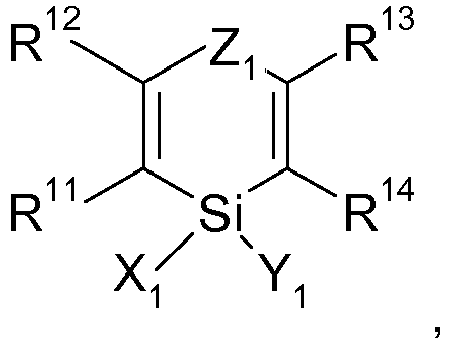
-
JP-A 2003243178 
- It is an object of the present application, with respect to the prior art, to provide novel device compositions for applications in organic electronics applications such as OLEDs, organic solar cells and switching elements, especially for OLEDs, which comprise materials for improvement of the performance of OLEDs, organic solar cells and switching elements, especially of OLEDs. The materials suitable for the novel device compositions should have good availability and stability and - in the case of OLEDs - result in high efficiencies and long lifetimes and low driving voltages in OLEDs, in combination with the emitters used in the OLEDs. More particularly, it is an object of the present application to provide materials which result in long lifetimes in OLEDs, organic solar cells and switching elements, especially in OLEDs. In addition, OLEDs with high efficiency and color purity are to be provided.
- This object is achieved by the provision of organic electronics applications, especially an organic light-emitting diode (OLED), an organic solar cell or a switching element, preferably an organic light-emitting diode (OLED), comprising at least one compound of the formula (I)

- R1, R2, R3, R4, R5, R6 and R7
are each independently hydrogen, C1-C20-alkyl, C3-C20-cycloalkyl, heterocycloalkyl having 3 to 20 ring atoms, C6-C30-aryl, heteroaryl having 5 to 30 ring atoms or a substituent with donor or acceptor action selected from the group consisting of C1-C20-alkoxy, C6-C30-aryloxy, C1-C20-alkylthio, C6-C30-arylthio, SiR10R11R12, halogen radicals, halogenated C1-C20-alkyl radicals, carbonyl (-CO(R10)), carbonylthio (- C = O (SR10)), carbonyloxy (- C = O(OR10)), oxycarbonyl (- OC = O(R10)), thiocarbonyl (- SC = O(R10)), amino (-NR10R11), OH, pseudohalogen radicals, amido (- C = O (NR10)), -NR10C = O (R11), phosphonate (-P(O)(OR10)2), phosphate (-OP(O)(OR10)2), phosphine (-PR10R11), phosphine oxide (-P(O)R10 2), sulfate (-OS(O)2OR10), sulfoxide (-S(O)R10), sulfonate (-S(O)2OR10), sulfonyl (-S(O)2R10), sulfonamide (-S(O)2NR10R11), NO2, boronic esters (-OB(OR10)2), imino (-C = NR10R11), borane radicals, stannane radicals, hydrazine radicals, hydrazone radicals, oxime radicals, nitroso groups, diazo groups, vinyl groups, sulfoximines, alanes, germanes, boroxines and borazines; or two adjacent R1, R2, R3, R4, R5, R6 or R7 radicals, in each case together with the carbon atoms to which they are bonded, form a ring having a total of 3 to 12 atoms, where the ring may be saturated or mono- or polyunsaturated and, as well as carbon atoms, may have one or more heteroatoms selected from N, O and P, where the ring may be unsubstituted or mono- or polysubstituted and/or may be fused to further 3- to 12-membered rings; - R8 and R9
are each independently C1-C20-alkyl, C3-C20-cycloalkyl, heterocycloalkyl having 3 to 20 ring atoms, C6-C30-aryl or heteroaryl having 5 to 30 ring atoms; - R10, R11, R12
are each independently C1-C20-alkyl, C3-C20-cycloalkyl, heterocycloalkyl having 3 to 20 ring atoms, C6-C30-aryl, heteroaryl having 5 to 30 ring atoms, -O-Si(C1-C20-alkyl)3, -O-Si(C6-C30-aryl)3, C1-C20-alkoxy or C6-C30-aryloxy;
or two adjacent R10 and R11, R10 and R12 or R11 and R12 radicals, together with the atom to which they are bonded, form a ring having a total of 3 to 12 atoms, where the ring may be saturated or mono- or polyunsaturated and, as well as the atom to which the R10, R11 or R12 radicals are bonded, may have exclusively carbon atoms or one or more further heteroatoms selected from N, O and P, where the ring may be unsubstituted or mono- or polysubstituted and/or may be fused to further 3- to 12-membered rings; - Y C2-C20-alkyl, C3-C20-cycloalkyl, heterocycloalkyl having 3 to 20 ring atoms, C6-C30-aryl, heteroaryl having 5 to 30 ring atoms or a substituent with donor or acceptor action selected from the group consisting of C1-C20-alkoxy, C6-C30-aryloxy, C1-C20-alkylthio, C6-C30-arylthio, SiR10R11R12, halogen radicals, halogenated C1-C20-alkyl radicals, carbonyl (-CO(R10)), carbonylthio (-C=O(SR10)), carbonyloxy (-C=O(OR10)), oxycarbonyl (-OC =O(R10)), thiocarbonyl (-SC=O(R10)), amino (-NR10R11), OH, pseudohalogen radicals, amido (-C=O(NR10)), -NR10C =O(R11), phosphonate (-P(O)(OR10)2), phosphate (-OP(O)(OR10)2), phosphine (-PR10R11), phosphine oxide (-P(O)R10 2), sulfate (-OS(O)2OR10), sulfoxide (-S(O)R10), sulfonate (-S(O)2OR10), sulfonyl (-S(O)2R10), sulfonamide (-S(O)2NR10R11), NO2, boronic esters (-OB(OR10)2), imino (-C=NR10R11), borane radicals, stannane radicals, hydrazine radicals, hydrazone radicals, oxime radicals, nitroso groups, diazo groups, vinyl groups, sulfoximines, alanes, germanes, boroxines and borazines; preferably heteroaryl having 5 to 30 ring atoms selected from the group consisting of pyrrolyl, furanyl, thienyl, benzoanellated ring systems of pyrrolyl, furanyl, thienyl, for example benzofuranyl, benzothienyl, indolyl, isoindolyl, isoindolizinyl, carbazolyl, azacarbazolyl, diazacarbazolyl, dibenzofuryl, dibenzothienyl, pyridyl, pyrimidyl, pyrazolyl, imidazolyl, thiazolyl, oxazolyl, triazolyl and phenanthrolinyl; or SiR10R11R12.
- Under the terms "electron/hole/exciton transport material" or layer, "electron/hole/exciton blocking material" or layer and "electron/hole/exciton injection material" or layer it is to be understood ""electron/exciton transport material" or layer or "hole/exciton transport material" or layer; "electron/exciton blocking material" or layer or "hole/exciton blocking material" or layer; respectively "electron /exciton injection material" or layer or "hole/exciton injection material" or layer.
- In the case of use of the phenoxasiline derivatives of the formula (I) in OLEDs, OLEDs are obtained which have good efficiencies and a long lifetime, and which can be operated especially at a low use and operating voltage. In addition, the OLEDs have a high color purity. The phenoxasiline derivatives of the formula (I) are especially suitable for use as host (matrix) and/or electron/hole/exciton transport material, electron/hole/exciton blocking materials and/or electron/hole injection materials for blue, green and red, especially blue emitters, for example light blue or deep blue emitters, these being especially phosphorescence emitters. The high triplet energy level of the phenoxasiline derivatives of formula (I) sufficiently confines light as well as deep blue excitons within the emissive layer. Therefore highly efficient blue light emitting OLEDs are obtained by employing the phenoxasiline derivatives of formula (I). In addition, the phenoxasiline derivatives of the formula (I) can be used as host (matrix) and/or electron/hole/exciton transport material, electron/hole/exciton blocking materials and/or electron/hole injection materials in organic electronics applications selected from switching elements and organic solar cells.
- The phenoxasiline derivatives of the formula (I) used in accordance with the invention can preferably be used as host (matrix) materials in the light-emitting layer E or any other layer of an OLED, preferably as host (matrix) materials in the light-emitting layer E, as an electron/hole/exciton transport material, as an electron/hole/exciton blocker or as electron/hole/exciton injection materials. Corresponding layers of OLEDs are known to those skilled in the art and are specified, for example, in
WO 2005/113704 orWO 2005/019373 . Preference is given to using the phenoxasiline derivatives of the formula (I) used in accordance with the invention as host (matrix) materials or electron/hole/exciton transport materials. - C1-C20-alkyl is understood to mean substituted or unsubstituted alkyl radicals having from 1 to 20 carbon atoms. Preference is given to C1- to C10-alkyl radicals, particular preference to C1- to C6-alkyl radicals. The alkyl radicals may be either straight-chain or branched or cyclic, where the alkyl radicals in the case of cyclic alkyl radicals have at least 3 carbon atoms. In addition, the alkyl radicals may be substituted by one or more substituents selected from the group consisting of C1-C20-alkoxy, halogen, preferably F, and C6-C30-aryl which may in turn be substituted or unsubstituted. Suitable aryl substituents and suitable alkoxy and halogen substituents are specified below. Examples of suitable alkyl groups are methyl, ethyl, propyl, butyl, pentyl, hexyl, heptyl and octyl, and also derivatives of the alkyl groups mentioned substituted by C6-C30-aryl, C1-C20-alkoxy and/or halogen, especially F, for example CF3. This includes both the n-isomers of the radicals mentioned and branched isomers such as isopropyl, isobutyl, isopentyl, sec-butyl, tert-butyl, neopentyl, 3,3-dimethylbutyl, 3-ethylhexyl, etc. Preferred alkyl groups are methyl, ethyl, tert-butyl and CF3.
- Examples of suitable cyclic alkyl groups (C3-C20-cycloalkyl), which may likewise be unsubstituted or substituted by the above radicals specified for the alkyl groups, are cyclopropyl, cyclobutyl, cyclopentyl, cyclohexyl, cycloheptyl, cyclooctyl, cyclononyl and cyclodecyl. These may optionally also be polycyclic ring systems, such as fluorenyl, decalinyl, norbornyl, bornanyl or adamantyl.
- Heterocycloalkyl with 3 to 20 ring atoms is understood to mean substituted or unsubstituted heterocycloalkyl having 3 to 20 ring atoms, which derive from the aforementioned cycloalkyl, wherein at least one atom of the ring atoms in the cycloalkyl base skeleton is replaced by a heteroatom. Preferred heteroatoms are N, O, Si and S. Preferred heterocycloalkyl radicals have a base skeleton selected from systems such as pyrrolidinyl, tetrahydofuryl, tetrahydrothienyl, piperidyl, tetrahydropyranyl, tetrahydrothiopyranyl, piperazinyl, morpholinyl, azasilinyl, oxasilinyl. These may optionally also be fused to form polycyclic ring sytems, e.g. fused to one or two six-membered aromatic radicals. Suitable fused systems are for example phenoxasilinyl or phenazasilinyl. The base skeleton may be substituted at one, more than one or all substitutable positions, suitable substituents being the same specified below under the definition of C6-C30-aryl. However, the heterocycloalkyl radicals are preferably unsubstituted or substituted by one of the substituents mentioned before.
- Preferred phenoxasilinyl groups are groups of the formula (I')

The symbol ∼ means that there is a binding site at the position marked with ∼. - Suitable C1-C20-alkoxy and C1-C20-alkylthio groups derive correspondingly from the aforementioned C1-C20-alkyl radicals. Examples here include OCH3, OC2H5, OC3H7, OC4H9 and OC8H17, and also SCH3, SC2H5, SC3H7, SC4H9 and SC8H17. C3H7, C4H9 and C8H17 include both the n-isomers and branched isomers such as iso-propyl, isobutyl, sec-butyl, tert-butyl and 2-ethylhexyl. Particularly preferred alkoxy or alkylthio groups are methoxy, ethoxy, n-octyloxy, 2-ethylhexyloxy and SCH3.
- Suitable halogen radicals or halogen substituents in the context of the present application are fluorine, chlorine, bromine and iodine, preferably fluorine, chlorine and bromine, more preferably fluorine and chlorine, most preferably fluorine.
- Suitable pseudohalogen radicals in the context of the present application are CN, SCN, OCN, N3 and SeCN, preference being given to CN and SCN. Very particular preference is given to CN.
- In the present invention, C6-C30-aryl refers to radicals which are derived from monocyclic, bicyclic or tricyclic aromatics which do not comprise any ring heteroatoms. When the system is not a monocyclic system, the saturated form (perhydro form) or the partly unsaturated form (for example the dihydro form or tetrahydro form) are also possible for the second ring in the case of the designation "aryl", provided that the particular forms are known and stable. In other words, the term "aryl" in the present invention also comprises, for example, bicyclic or tricyclic radicals in which either both or all three radicals are aromatic, and also bicyclic or tricyclic radicals in which only one ring is aromatic, and also tricyclic radicals in which two rings are aromatic. Examples of aryl are: phenyl, naphthyl, indanyl, 1,2-dihydronaphthenyl, 1,4-dihydronaphthenyl, indenyl, anthracenyl, phenanthrenyl or 1,2,3,4-tetrahydronaphthyl. Particular preference is given to C6-C10-aryl radicals, for example phenyl or naphthyl, very particular preference to C6-aryl radicals, for example phenyl.
- The C6-C30-aryl radicals may be unsubstituted or substituted by one or more further radicals. Suitable further radicals are selected from the group consisting of C1-C20-alkyl, C3-C20-cycloalkyl, heterocycloalkyl having 3 to 20 ring atoms, C6-C30-aryl or substituents with donor or acceptor action, suitable substituents with donor or acceptor action being specified below. The C6-C30-aryl radicals are preferably unsubstituted or substituted by one or more C1-C20-alkoxy groups, CN, CF3, F or amino groups (NR10R11, where suitable R10 and R11 radicals are specified above). Most preferably is unsubstituted phenyl or phenyl substituted with a phenoxasilinyl group, whereby a preferred phenoxasilinyl group is a phenoxasilinyl group of formula (I') as mentioned before.
- Suitable C6-C30-aryloxy, C6-C30-alkylthio radicals derive correspondingly from the aforementioned C6-C30-aryl radicals. Particular preference is given to phenoxy and phenylthio.
- Heteroaryl having from 5 to 30 ring atoms is understood to mean unsubstituted or substituted monocyclic, bicyclic or tricyclic heteroaromatics which derive from the aforementioned aryl, in which at least one carbon atom in the aryl base skeleton has been replaced by a heteroatom. Preferred heteroatoms are N, O, Si and S. The heteroaryl radicals more preferably have from 5 to 13 ring atoms. Especially preferably, the base skeleton of the heteroaryl radicals is selected from systems such as pyridine and five-membered heteroaromatics such as thiophene, pyrrole, imidazole, silole or furan. These base skeletons may optionally be fused to one or two six-membered aromatic radicals. Suitable fused heteroaromatics are carbazolyl, azacarbazolyl, diazacarbazolyl, benzimidazolyl, benzofuryl, dibenzofuryl or dibenzothiophenyl. The base skeleton may be substituted at one, more than one or all substitutable positions, suitable substituents being the same as have already been specified under the definition of C6-C30-aryl. However, the heteroaryl radicals are preferably unsubstituted or substituted with a phenoxasilinyl group, whereby a preferred phenoxasilinyl group is a phenoxasilinyl group of formula (I') as mentioned before. Suitable heteroaryl radicals are, for example, pyridin-2-yl, pyridin-3-yl, pyridin-4-yl, thiophen-2-yl, thiophen-3-yl, pyrrol-2-yl, pyrrol-3-yl, furan-2-yl, furan-3-yl and imidazol-2-yl, and also the corresponding benzofused radicals, especially carbazolyl, azacarbazolyl, diazacarbazolyl, benzimidazolyl, benzofuryl, dibenzofuryl or dibenzothiophenyl. Further preferred heteroaryl radicals are mentioned below in the discussion of the specific radicals of the compound of formula (I).
In the context of the present application, groups with donor or acceptor action are understood to mean the following groups:
C1-C20-alkoxy, C6-C30-aryloxy, C1-C20-alkylthio, C6-C30-arylthio, SiR10R11R12, halogen radicals, halogenated C1-C20-alkyl radicals, carbonyl (-CO(R10)), carbonylthio (- C = O (SR10)), carbonyloxy (- C = O(OR10)), oxycarbonyl (- OC = O(R10)), thiocarbonyl (- SC = O(R10)), amino (-NR10R11), OH, pseudohalogen radicals, amido (- C = O (NR10)), -NR10C = O (R11), phosphonate (- P(O) (OR10)2), phosphate (-OP(O) (OR10)2), phosphine (-PR10R11), phosphine oxide (-P(O)R10 2), sulfate (-OS(O)2OR10), sulfoxide (-S(O)R10), sulfonate (-S(O)2OR10), sulfonyl (-S(O)2R10), sulfonamide (-S(O)2NR10R11), NO2, boronic esters (-OB(OR10)2), imino (-C = NR10R11), borane radicals, stannane radicals, hydrazine radicals, hydrazone radicals, oxime radicals, nitroso groups, diazo groups, vinyl groups, and boronic acid groups, sulfoximines, alanes, germanes, boroxines and borazines.
Preferred substituents with donor or acceptor action are selected from the group consisting of: C1- to C20-alkoxy, preferably C1-C6-alkoxy, more preferably ethoxy or methoxy; C6-C30-aryloxy, preferably C6-C10-aryloxy, more preferably phenyloxy; SiR10R11R12 where R10, R11 and R12 are preferably each independently substituted or unsubstituted alkyl or substituted or unsubstituted phenyl; more preferably, at least one of the R10, R11 or R12 radicals is substituted or unsubstituted phenyl; most preferably, at least one of the R10, R11 or R12 radicals is substituted phenyl, where suitable substituents have been specified above; halogen radicals, preferably F, Cl, Br, more preferably F or Cl, most preferably F, halogenated C1-C20-alkyl radicals, preferably halogenated C1-C6-alkyl radicals, most preferably fluorinated C1-C6-alkyl radicals, e.g. CF3, CH2F, CHF2 or C2F5; amino, preferably dimethylamino, diethylamino or diphenylamino; OH, pseudohalogen radicals, preferably CN, SCN or OCN, more preferably CN, -C(O)OC1-C4-alkyl, preferably -C(O)OMe, P(O)R2, preferably P(O)Ph2 or SO2R2, preferably SO2Ph.
Very particularly preferred substituents with donor or acceptor action are selected from the group consisting of methoxy, phenyloxy, halogenated C1-C4-alkyl, preferably CF3, CH2F, CHF2, C2F5, halogen, preferably F, CN, SiR10R11R12, diphenylamino, -C(O)OC1-C4-alkyl, preferably-C(O)OMe, P(O)Ph2, SO2Ph.
The aforementioned groups with donor or acceptor action are not intended to rule out the possibility that further aforementioned radicals and groups may also have donor or acceptor action. For example, the aforementioned heteroaryl radicals are likewise groups with donor or acceptor action, and the C1-C20-alkyl radicals are groups with donor action.
The R10, R11 and R12 radicals mentioned in the aforementioned groups with donor or acceptor action each have the definitions which have already been mentioned above and are mentioned below.
Preferably, R10, R11, R12 are each independently C6-C30-aryl, more preferably phenyl, which is even more preferably unsubstituted.
The radical Y in the phenoxasiline derivatives of the formula (I) is C2-C20-alkyl, C3-C20-cycloalkyl, heterocycloalkyl having 3 to 20 ring atoms, C6-C30-aryl, heteroaryl having 5 to 30 ring atoms or a substituent with donor or acceptor action selected from the group consisting of C1-C20-alkoxy, C6-C30-aryloxy, C1-C20-alkylthio, C6-C30-arylthio, SiR10R11R12, halogen radicals, halogenated C1-C20-alkyl radicals, carbonyl (-CO(R10)), carbonylthio (- C = O (SR10)), carbonyloxy (- C = O(OR10)), oxycarbonyl (- OC = O(R10)), thiocarbonyl (- SC = O(R10)), amino (-NR10R11), OH, pseudohalogen radicals, amido (- C = O (NR10)), -NR10C = O (R11), phosphonate (- P(O) (OR10)2), phosphate (-OP(O) (OR10)2), phosphine (-PR10R11), phosphine oxide (-P(O)R10 2), sulfate (-OS(O)2OR10), sulfoxide (-S(O)R10), sulfonate (-S(O)2OR10), sulfonyl (-S(O)2R10), sulfonamide (-S(O)2NR10R11), NO2, boronic esters (-OB(OR10)2), imino (-C = NR10R11), borane radicals, stannane radicals, hydrazine radicals, hydrazone radicals, oxime radicals, nitroso groups, diazo groups, vinyl groups, sulfoximines, alanes, germanes, boroxines and borazines; and
R10, R11 and R12 are each independently C1-C20-alkyl, C3-C20-cycloalkyl, heterocycloalkyl having 3 to 20 ring atoms, C6-C30-aryl, heteroaryl having 5 to 30 ring atoms, -O-Si(C1-C20-alkyl)3, -O-Si(C6-C30-aryl)3, C1-C20-alkoxy or C6-C30-aryloxy; preferably C6-C30-aryl, more preferably phenyl; or two adjacent R10 and R11, R10 and R12 or R11 and R12 radicals, together with the atom to which they are bonded, form a ring having a total of 3 to 12 atoms, where the ring may be saturated or mono- or polyunsaturated and, as well as the atom to which the R10, R11 or R12 radicals are bonded, may have exclusively carbon atoms or one or more further heteroatoms selected from N, O and P, where the ring may be unsubstituted or mono- or polysubstituted and/or may be fused to further 3- to 12-membered rings.
Preferably, Y is heteroaryl having 5 to 30 ring atoms selected from the group consisting of pyrrolyl, furanyl, thienyl, benzoanellated ring systems of pyrrolyl, furanyl, thienyl, for example benzofuranyl, benzothienyl, indolyl, isoindolyl, isoindolizinyl, carbazolyl, azacarbazolyl, diazacarbazolyl, dibenzofuryl, dibenzothienyl, pyridyl, pyrimidyl, pyrazolyl, imidazolyl, thiazolyl, oxazolyl, triazolyl and phenanthrolinyl; or SiR10R11R12; and
R10, R11 and R12 are each independently C6-C30-aryl, preferably phenyl.
More preferably, Y is selected from the group consisting of unsubstituted or substituted pyrrolyl, furanyl, thienyl, benzofuranyl, benzothienyl, indolyl, isoindolyl, isoindolizinyl, carbazolyl, azacarbazolyl, diazacarbazolyl, dibenzofuryl, dibenzothienyl and SiPh3.
Even more preferably, Y is selected from the group consisting of


wherein - X
- is NR10, O or S,
- R10
- is C1-C20-alkyl, C6-C30-aryl, heteroaryl having 5 to 30 ring atoms, -O-Si(C1-C20-alkyl)3, -O-Si(C6-C30-aryl)3, C1-C20-alkoxy or C6-C30-aryloxy; preferably C6-C30-aryl, more preferably phenyl, and
- R13
- is H or phenoxasilinyl of formula (I'), preferably H.
- The symbol ∼ means that there is a binding site at the position marked with ∼.
- R8 and R9 in the phenoxasilines of formula (I) are each independently C1-C20-alkyl, C6-C30-aryl, heteroaryl having 5 to 30 ring atoms.
- Preferably, R8 and R9 are each independently C6-C30-aryl or heteroaryl having 5 to 30 ring atoms.
- More preferably, R8 and R9 are each independently phenyl, which is most preferably unsubstituted, dibenzofuranyl or carbazolyl.
- Even more preferably, R8 and R9 are each independently unsubstituted phenyl,
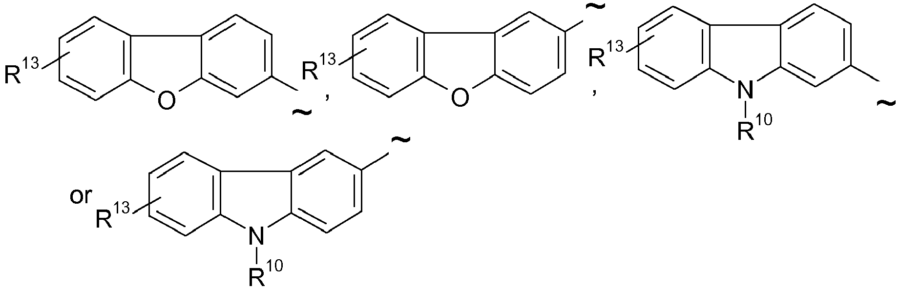
- R13
- is H or phenoxasilinyl of formula (I'), preferably H.
- The symbol ∼ means that there is a binding site at the position marked with ∼. In a preferred embodiment, R8 and R9 in the compounds of formula (I) are identical.
- R1, R2, R3, R4, R5, R6 and R7 in the phenoxasiline derivatives of the formula (I) are each independently hydrogen, C1-C20-alkyl, C3-C20-cycloalkyl, heterocycloalkyl having 3 to 20 ring atoms, C6-C30-aryl, heteroaryl having 5 to 30 ring atoms or a substituent with donor or acceptor action selected from the group consisting of C1-C20-alkoxy, C6-C30-aryloxy, C1-C20-alkylthio, C6-C30-arylthio, SiR10R11R12, halogen radicals, halogenated C1-C20-alkyl radicals, carbonyl (-CO(R10)), carbonylthio (-C=O(SR10)), carbonyloxy (-C=O(OR10)), oxycarbonyl (-OC=O(R10)), thiocarbonyl (-SC=O(R10)), amino (-NR10R11), OH, pseudohalogen radicals, amido (-C=O (NR10)), -NR10C =O(R11), phosphonate (-P(O)(OR10)2), phosphate (-OP(O)(OR10)2), phosphine (-PR10R11), phosphine oxide (-P(O)R10 2), sulfate (-OS(O)2OR10), sulfoxide (-S(O)R10), sulfonate (-S(O)2OR10), sulfonyl (-S(O)2R10), sulfonamide (-S(O)2NR10R11), NO2, boronic esters (-OB(OR10)2), imino (-C=NR10R11), borane radicals, stannane radicals, hydrazine radicals, hydrazone radicals, oxime radicals, nitroso groups, diazo groups, vinyl groups, sulfoximines, alanes, germanes, boroxines and borazines;
or two adjacent R1, R2, R3, R4, R5, R6 or R7 radicals, in each case together with the carbon atoms to which they are bonded, form a ring having a total of 3 to 12 atoms, where the ring may be saturated or mono- or polyunsaturated and, as well as carbon atoms, may have one or more heteroatoms selected from N, O and P, where the ring may be unsubstituted or mono- or polysubstituted and/or may be fused to further 3- to 12-membered rings.
Preferably, R1, R2, R3, R4, R5, R6 and R7 are each independently hydrogen, C1-C20-alkyl, C3-C20-cycloalkyl, heterocycloalkyl having 3 to 20 ring atoms, C6-C30-aryl, heteroaryl having 5 to 30 ring atoms, methoxy, phenyloxy, halogenated C1-C4-alkyl, preferably CF3, CH2F, CHF2, C2F5, halogen, preferably F, CN, SiR10R11R12, diphenylamino or -C(O)OC1-C4-alkyl, preferably -C(O)OMe, P(O)Ph2, SO2Ph.
More preferably, R1, R2, R3, R4, R5, R6 and R7 are each independently hydrogen, C1-C20-alkyl, C3-C20-cycloalkyl, heterocycloalkyl having 3 to 20 ring atoms, C6-C30-aryl, heteroaryl having 5 to 30 ring atoms, methoxy, phenyloxy, halogenated C1-C4-alkyl, preferably CF3, CH2F, CHF2, C2F5, halogen, preferably F, CN, SiR10R11R12, P(O)Ph2 or diphenylamino.
In one preferred embodiment, R1, R2, R3, R4, R5, R6 and R7 are each hydrogen or R1, R2, R5, R6 and R7 are each hydrogen and R3 and R4 are each independently C1-C20-alkyl, C3-C20-cycloalkyl, heterocycloalkyl having 3 to 20 ring atoms, C6-C30-aryl, heteroaryl having 5 to 30 ring atoms, methoxy, phenyloxy, halogenated C1-C4-alkyl, preferably CF3, CH2F, CHF2, C2F5, halogen, preferably F, CN, SiR10R11R12, P(O)Ph2 or diphenylamino, preferably methyl, phenyl, carbazolyl, dibenzofuryl, methoxy, phenyloxy, CF3, CH2F, CHF2, C2F5, F, CN, SiR10R11R12, P(O)Ph2 or diphenylamino. R3 and R4 may be identical or different.
In one further preferred embodiment, one of the radicals R1, R2, R3, R4, R5, R6 and R7 has the meaning mentioned before, except of hydrogen, preferably C1-C20-alkyl, C3-C20-cycloalkyl, heterocycloalkyl having 3 to 20 ring atoms, C6-C30-aryl, heteroaryl having 5 to 30 ring atoms, methoxy, phenyloxy, halogenated C1-C4-alkyl, preferably CF3, CH2F, CHF2, C2F5, halogen, preferably F, CN, SiR10R11R12, P(O)Ph2 or diphenylamino and all other radicals R1, R2, R3, R4, R5, R6 and R7 are hydrogen. Preferably, the radical which is not hydrogen is the radical R6. More preferably, the radical R6 has the same meaning as Y. Preferred meanings for Y are also preferred meanings for R6. Y and R6 may be identical or different. - In a further preferred embodiment, R6 as well as R3 and R4 have the meanings mentioned before, except of hydrogen, preferably, R3 and R4 are C1-C20-alkyl, C3-C20-cycloalkyl, heterocycloalkyl having 3 to 20 ring atoms, C6-C30-aryl, heteroaryl having 5 to 30 ring atoms, methoxy, phenyloxy, halogenated C1-C4-alkyl, preferably CF3, CH2F, CHF2, C2F5, halogen, preferably F, CN, SiR10R11R12, P(O)Ph2 or diphenylamino and all other radicals R1, R2, R5 and R7 are hydrogen. R3 and R4 may be identical or different. More preferably, the radical R6 has the same meaning as Y. Preferred meanings for Y are also preferred meanings for R6. Y and R6 may be identical or different. Even more preferably, R3 and R4 are each independently methyl, phenyl, carbazolyl, dibenzofuryl, methoxy, phenyloxy, CF3, CH2F, CHF2, C2F5, F, CN, SiR10R11R12, P(O)Ph2 or diphenylamino.
- In a preferred embodiment of the present invention, the compound of formula (I) is selected from the compounds of formulae (Ia), (Ib), (Ic) and (Id)


- In a more preferred embodiment of the present invention, the compound of formula (I) is selected from the compounds of formulae (Ib) and (Id).
- Examples for most preferred compounds of the formula (I) are


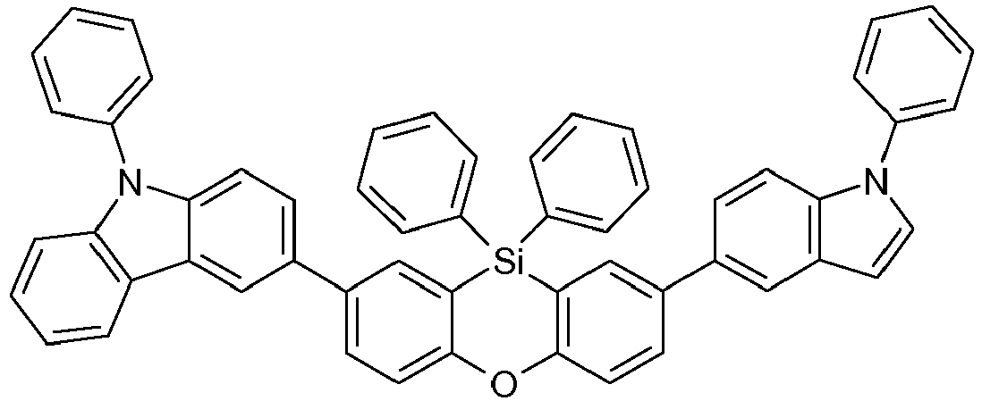


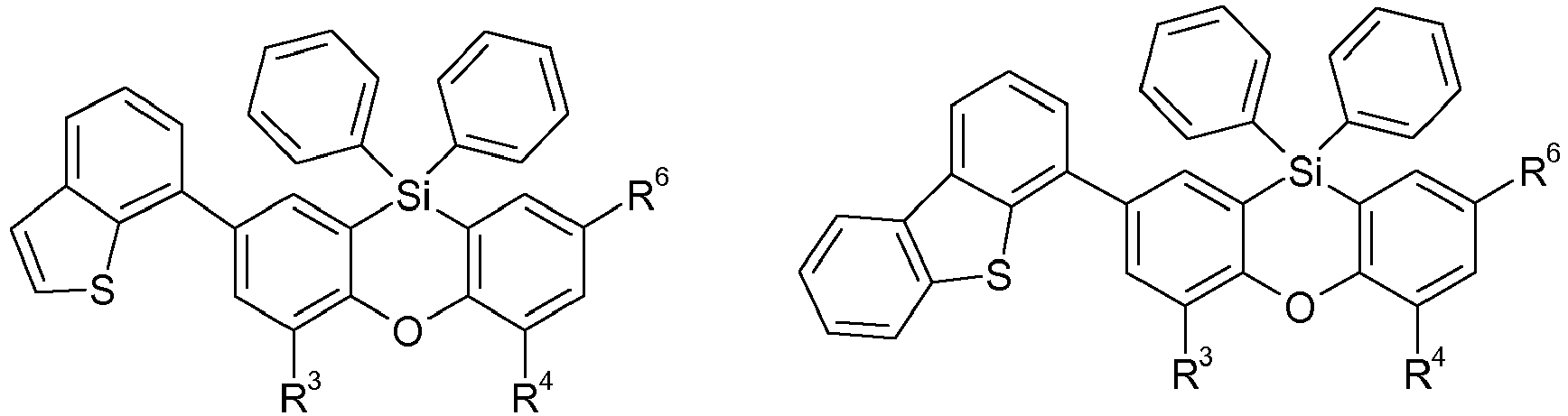


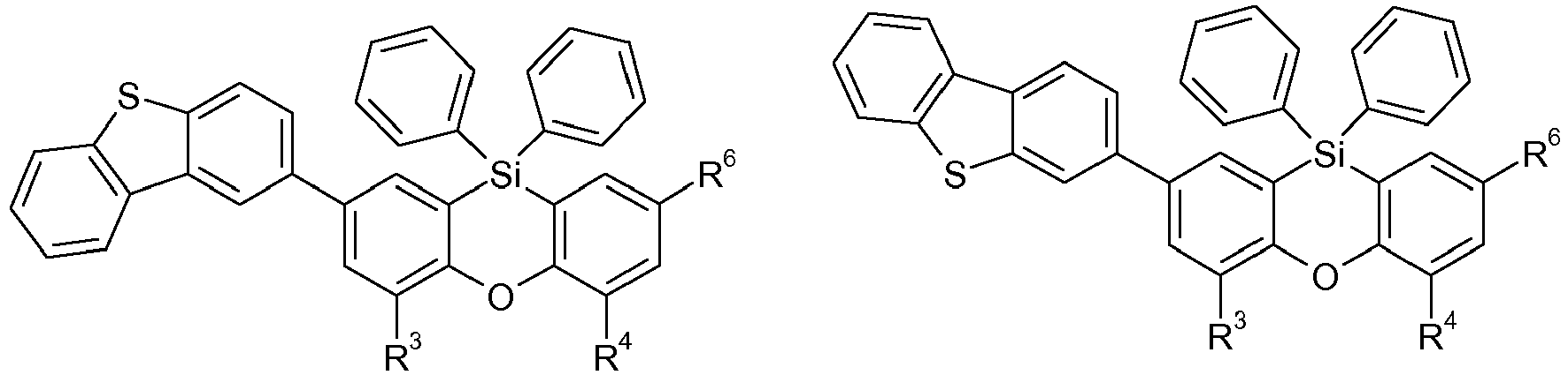


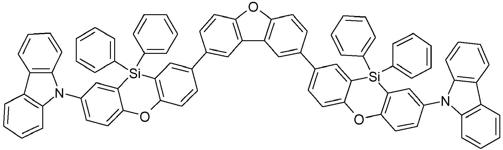


- R6
- is selected from the group consisting of hydrogen,
- X
- is NPh, O or S,
- R3, R4
- are independently of each other methyl, phenyl, carbazolyl, dibenzofuryl, methoxy, phenyloxy, CF3, CH2F, CHF2, C2F5, F, CN, SiR10R11R12, P(O)Ph2 or diphenylamino, and
- R13
- is H or phenoxasilinyl of formula (I'), preferably H.
- The symbol ∼ means that there is a binding site at the position marked with ∼.
- Preferably, R6 is selected from the group consisting of

wherein - X
- is NPh or O, and
- R13
- is H or phenoxasilinyl of formula (I'), preferably H.
- The symbol ∼ means that there is a binding site at the position marked with ∼.
- Most preferred compounds of the formula (I) are


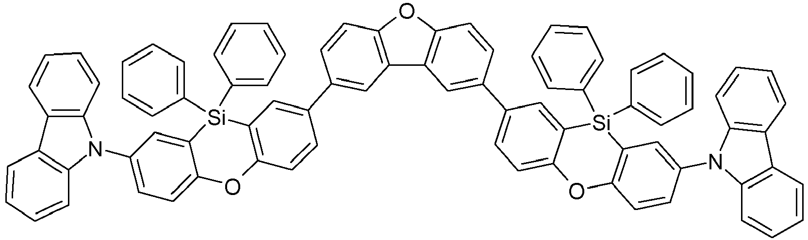


- The compounds of the formula (I) can be prepared by the following process:
- I) Preparation of a functionalized phenoxasiline building block (A)

In the case that R6 is H, the Hal substituent at the position of R6 has to be replaced by H.
wherein the radicals R1, R2, R3, R4, R5, R7, R8 and R9 have the meanings mentioned above, and
Hal is Br or Cl.- Ii) Step i) Preparation of a halogenated diphenyl ether

- Hal2
- is Br2 or Cl2
- cat.
- is a catalyst, preferably Fe, and
- solvent
- is a solvent, preferably an aprotic solvent, more preferably CCl4.
The catalyst is usually employed in catalytic amounts relative to the diphenyl ether (molar ratio). The molar ratio of catalyst to diphenyl ether is preferably 0.01 to 0.1 : 1, more preferably 0.03 to 0.08: 1.
The Hal2 is usually employed in an excess relative to the diphenyl ether (molar ratio). The molar ratio of Hal2 to diphenyl ether is preferably 1.5 to 10 : 1, more preferably 2.5 to 8 : 1. - lii) Step ii) Preparation of a functionalized phenoxasiline building block (A)

- Hal
- is Br or Cl
- base
- is a base, preferably n-BuLi, and
- solvent
- is a protic solvent, preferably Et2O.
The R8 2SiHal2 and/or R9 2SiHal2 is usually employed in equimolar amounts relative to the halogenated diphenyl ether (molar ratio). The molar ratio of R8 2SiHal2 and/or R9 2SiHal2 to halogenated diphenyl ether is preferably 1.5 : 1, more preferably 1.3 to 1 : 1. If R8 2SiHal2 and R9 2SiHal2 are employed, R8 2SiHal2 and R9 2SiHal2 are employed in equimolar amounts and the sum of R8 2SiHal2 and R9 2SiHal2 is the molar amount mentioned before in relation to the halogenated diphenyl ether. - liii) Step iii) Introduction of R3 and R4 into building block (A)
In the case that R3 and/or R4 in the compound of formula (I) are not hydrogen and are not present in building block (A) at the end of step ii), the functionalization of the ortho position in building block (A) (i.e. the position of R3 and R4) can be carried out as described for example in Advanced Synthesis & Catalysis 353(9), 1479-1484, 2011 and Angewandte Chemie, International Edition, 45(35), 5803-5807; 2006.
In a typical procedure a deprotonation and activation of the ortho position in building block (A) is carried out by deprotonation with for example s-butyl lithium in for example TMEDA (tetramethylethylene diamine) and activation with chloride (e.g. by addition of PPh2Cl or SiPh3Cl) or iodide (e.g. by addition of alkyl iodide, e.g. methyl iodide).
The activated ortho position can then be substituted as known by a person skilled in the art, for example in the case of a functionalization with P(O)Ph2, by functionalization with PPh2Cl and a subsequent oxidation with for example mCPBA (meta-chloroperbenzoic acid).
It is also possible to carry step liii) out after the coupling in step II) is carried out.
- Ii) Step i) Preparation of a halogenated diphenyl ether
- II) Preparation of the phenoxasilines according to the present invention
The functionalized phenoxasiline building block (A) is the preferred starting material for the preparation of the compounds of formula (I) of the present invention. The groups Y and (optionally) R6 are introduced into the building block (A) by coupling methods known by a person skilled in the art. In the examples the introduction of three different ligand types is described:- i) Groups Y and R6 are bonded via a heteroatom in a heterocyclic ring system (e.g. carbazolyl bonded via N; compound (1)). Such groups are preferably introduced into the building block (A) by Ullmann coupling or Buchwald coupling. An example for a suitable coupling reaction is given in synthesis example 1.2.
- ii) Groups Y and R6 are bonded via a heteroatom which is not in a heterocyclic ring system (e.g. -SiPh3 bonded via Si; compound (2)). Such coupling reactions are known to a person skilled in the art. An example for a suitable coupling reaction is given in synthesis example 1.3.
- iii) Groups Y and R6 are bonded via an aromatic carbon atom (e.g. dibenzofuranyl bonded via an aromatic C; compound (3)). Such groups are preferably introduced into the building block (A) by Suzuki coupling or Yamamoto coupling. An example for a suitable coupling reaction is given in synthesis example I.4.
- The phenoxasiline derivatives of the general formula (I) are suitable for use in organic electronics applications, especially in OLEDs. Further organic electronics applications have been mentioned before.
- The phenoxasiline derivatives of the general formula (I) are useful in any layer of organic electronic applications, especially OLEDs. Preferably, the phenoxasiline derivatives of the general formula (I) are employed as host (matrix) material, preferably in the light-emitting layer, in OLEDs, or as electron/hole/exciton transport material, or as electron/hole/exciton blocker material or electron/hole/exciton injection material in the respective layer of organic electronics applications, especially OLEDs or as organic semiconductor layer.
- Suitable structures of the organic electronics applications are known to those skilled in the art and are specified below.
- The organic transistor generally includes a semiconductor layer formed from an organic layer with hole transport capacity and/or electron transport capacity; a gate electrode formed from a conductive layer; and an insulation layer introduced between the semiconductor layer and the conductive layer. A source electrode and a drain electrode are mounted on this arrangement in order thus to produce the transistor element. In addition, further layers known to those skilled in the art may be present in the organic transistor. The compounds of the formula (I) may be present in any desired layer of the organic transistor.
- The organic solar cell (photoelectric conversion element) generally comprises an organic layer present between two plate-type electrodes arranged in parallel. The organic layer may be configured on a comb-type electrode. There is no particular restriction regarding the site of the organic layer and there is no particular restriction regarding the material of the electrodes. When, however, plate-type electrodes arranged in parallel are used, at least one electrode is preferably formed from a transparent electrode, for example an ITO electrode or a fluorine-doped tin oxide electrode. The organic layer is formed from two sublayers, i.e. a layer with p-type semiconductor character or hole transport capacity, and a layer formed with n-type semiconductor character or electron transport capacity. In addition, it is possible for further layers known to those skilled in the art to be present in the organic solar cell. The compounds of the formula (I) may be present in any desired layer of the organic solar cell.
- Preferably, the present invention relates to an organic light-emitting diode comprising at least one compound of the formula (I). The compounds of the formula (I) can be used in the organic light-emitting diode as host (matrix) material and/or hole/exciton blocker material and/or electron/exciton blocker material and/or hole injection material and/or electron injection material and/or hole conductor material and/or electron conductor material, preferably as host (matrix) material, preferably in the light-emitting layer, and/or as electron/hole/exciton transport material and/or as electron/hole/exciton blocker material and/or electron/hole/exciton injection material.
- The present invention therefore relates to the inventive organic electronics applications, wherein at least one compound of formula (I) is employed as host (matrix) material, preferably in the light-emitting layer, and/or as electron/hole/exciton transport material and/or as electron/hole/exciton blocker material and/or electron/hole/exciton injection material.
- The present invention further relates to host (matrix) material and/or electron/hole/exciton transport material and/or electron/hole/exciton blocker material and/or electron/hole/exciton injection material in organic electronics applications comprising at least one compound of the formula (I) according to the present invention.
- The compounds of the general formula (I) may be employed alone or in a mixture, for example together with another host (matrix) material, electron/hole/exciton transport material, electron/hole/exciton blocker material or electron/hole/exciton injection material. Further host (matrix) material, electron/hole/exciton transport material, electron/hole/exciton blocker material and electron/hole/exciton injection material used may generally be materials known to those skilled in the art, especially the host (matrix) material, electron/hole/exciton transport material, electron/hole/exciton blocker material and electron/hole/exciton injection material mentioned below.
- It is likewise possible that the compounds of the formula (I) are present in more than one layer of the organic electronics applications, especially OLEDs, for example in both in the light-emitting layer (as host (matrix) material) and in the blocking layer for holes.
- In a further embodiment, the present invention concerns the use of a compound of formula (I) according to the present invention in organic electronics applications. Suitable organic electronics applications are mentioned before. Preferred organic electronics applications are OLEDs.
- The present invention further provides an organic light-emitting diode comprising an anode An and a cathode Ka and a light-emitting layer E arranged between the anode An and the cathode Ka, and optionally at least one further layer selected from the group consisting of at least one blocking layer for holes/excitons, at least one blocking layer for electrons/excitons, at least one hole injection layer, at least one hole conductor (transport) layer, at least one electron injection layer and at least one electron conductor (transport) layer, wherein the at least one compound of the formula (I) is present in the light-emitting layer E and/or in at least one of the further layers. The at least one compound of the formula (I) is preferably present in the light-emitting layer as a host and/or in the blocking layer for holes/excitons. The at least one compound of the formula (I) may further or additionally be present in the electron/exciton transport layer, hole/exciton transport layer, electron/ exciton blocking layer, hole/exciton injection layer and/or electron/exciton injection layer
- The present application further relates to a light-emitting layer comprising at least one compound of the formula (I), preferably as host.
- The present invention further relates to an OLED comprising an inventive light-emitting layer.
- The present invention further relates to a electron/exciton transport layer or hole/exciton transport layer comprising at least one compound of the formula (I).
- The present invention further relates to a blocking layer for holes/excitons or a blocking layer for electrons/excitons comprising at least one compound of the formula (I).
- The present invention further relates to an injection layer for holes/excitons or an injection layer for electrons/excitons comprising at least one compound of the formula (I).
- The inventive organic light-emitting diode (OLED) thus generally has the following structure:
An anode (An) and a cathode (Ka) and a light-emitting layer E arranged between the anode (An) and the cathode (Ka). - The inventive OLED may, for example - in a preferred embodiment - be formed from the following layers:
- 1. anode
- 2. hole conductor (transport) layer
- 3. light-emitting layer
- 4. blocking layer for holes/excitons
- 5. electron conductor (transport) layer
- 6. cathode
- It is additionally possible that a plurality of the aforementioned functions (electron/exciton blocker, hole/exciton blocker, hole injection, hole conduction, electron injection, electron conduction) are combined in one layer and are assumed, for example, by a single material present in this layer. For example, a material used in the hole conductor layer, in one embodiment, may simultaneously block excitons and/or electrons.
- Furthermore, the individual layers of the OLED among those specified above may in turn be formed from two or more layers. For example, the hole conductor layer may be formed from a layer into which holes are injected from the electrode, and a layer which transports the holes away from the hole-injecting layer into the light-emitting layer. The electron conduction layer may likewise consist of a plurality of layers, for example a layer in which electrons are injected by the electrode, and a layer which receives electrons from the electron injection layer and transports them into the light-emitting layer. These layers mentioned are each selected according to factors such as energy level, thermal resistance and charge carrier mobility, and also energy difference of the layers specified with the organic layers or the metal electrodes. The person skilled in the art is capable of selecting the structure of the OLEDs such that it is matched optimally to the organic compounds used as emitter substances in accordance with the invention.
- In order to obtain particularly efficient OLEDs, for example, the HOMO (highest occupied molecular orbital) of the hole conductor layer should be matched to the work function of the anode, and the LUMO (lowest unoccupied molecular orbital) of the electron conductor layer should be matched to the work function of the cathode, provided that the aforementioned layers are present in the inventive OLEDs.
- The anode (1) is an electrode which provides positive charge carriers. It may be formed, for example, from materials which comprise a metal, a mixture of various metals, a metal alloy, a metal oxide or a mixture of various metal oxides. Alternatively, the anode may be a conductive polymer. Suitable metals comprise metals and alloys of the metals of the main groups, transition metals and of the lanthanoids, especially the metals of groups Ib, IVa, Va and Via of the periodic table of the elements, and the transition metals of group Villa. When the anode is to be transparent, generally mixed metal oxides of groups IIb, IIIb and IVb of the Periodic Table of the Elements (old IUPAC version) are used, for example indium tin oxide (ITO). It is likewise possible that the anode (1) comprises an organic material, for example polyaniline, as described, for example, in Nature, vol. 357, pages 477 to 479 (June 11, 1992). At least either the anode or the cathode should be at least partly transparent in order to be able to emit the light formed. The material used for the anode (1) is preferably ITO.
- Suitable hole conductor materials for layer (2) of the inventive OLEDs are disclosed, for example, in Kirk-Othmer Encyclopedia of Chemical Technology, 4th edition, vol. 18, pages 837 to 860, 1996. Both hole-transporting molecules and polymers can be used as hole transport material. Hole-transporting molecules typically used are selected from the group consisting of tris[N-(1-naphthyl)-N-(phenylamino)]triphenylamine (1-NaphDATA), 4,4'-bis[N-(1-naphthyl)-N-phenylamino]biphenyl (a-NPD), N,N'-diphenyl-N,N'-bis(3-methylphenyl)-[1,1'-biphenyl]-4,4'-diamine (TPD), 1,1-bis[(di-4-tolylamino)phenyl]cyclohexane (TAPC), N,N'-bis(4-methylphenyl)-N,N'-bis(4-ethylphenyl)-[1,1'-(3,3'-dimethyl)biphenyl]-4,4'-diamine (ETPD), tetrakis(3-methylphenyl)-N,N,N',N'-2,5-phenylenediamine (PDA), α-phenyl-4-N,N-diphenylaminostyrene (TPS), p-(diethylamino)benzaldehyde diphenylhydrazone (DEH), triphenylamine (TPA), bis[4-(N,N-diethylamino)-2-methylphenyl)](4-methylphenyl)methane (MPMP), 1-phenyl-3-[p-(diethylamino)styryl]-5-[p-(diethylamino)phenyl]pyrazoline (PPR or DEASP), 1,2-trans-bis(9H-carbazol-9-yl)cyclobutane (DCZB), N,N,N',N'-tetrakis(4-methylphenyl)-(1,1'-biphenyl)-4,4'-diamine (TTB), 4,4',4"-tris(N,N-diphenylamino)triphenylamine (TDTA), 4,4',4"-tris(N-carbazolyl)triphenylamine (TCTA), N,N'-bis(naphthalen-2-yl)-N,N'-bis(phenyl)benzidine (β-NPB), N,N'-bis(3-methylphenyl)-N,N'-bis(phenyl)-9,9-spirobifluorene (spiro-TPD), N,N'-bis(naphthalen-1-yl)-N,N'-bis(phenyl)-9,9-spirobifluorene (spiro-NPB), N,N'-bis(3-methylphenyl)-N,N'-bis(phenyl)-9,9-dimethylfluorene (DMFL-TPD), di[4-(N,N-ditolylamino)phenyl]cyclohexane, N,N'-bis(naphthalen-1-yl)-N,N'-bis(phenyl)-9,9-dimethylfluorene, N,N'-bis(naphthalen-1-yl)-N,N'-bis(phenyl)-2,2-dimethylbenzidine, N,N'-bis(naphthalen-1-yl)-N,N'-bis(phenyl)benzidine, N,N'-bis(3-methylphenyl)-N,N'-bis(phenyl)benzidine, 2,3,5,6-tetrafluoro-7,7,8,8-tetracyanoquinodimethane (F4-TCNQ), 4,4',4"-tris(N-3-methylphenyl-N-phenylamino)triphenylamine, 4,4',4"-tris(N-(2-naphthyl)-N-phenyl-amino)triphenylamine, pyrazino[2,3-f][1,10]phenanthroline-2,3-dicarbonitrile (PPDN), N,N,N',N'-tetrakis(4-methoxyphenyl)benzidine (MeO-TPD), 2,7-bis[N,N-bis(4-methoxyphenyl)amino]-9,9-spirobifluorene (MeO-spiro-TPD), 2,2'-bis[N,N-bis(4-methoxyphenyl)amino]-9,9-spirobifluorene (2,2'-MeO-spiro-TPD), N,N'-diphenyl-N,N'-di[4-(N,N-ditolylamino)phenyl]benzidine (NTNPB), N,N'-diphenyl-N,N'-di[4-(N,N-diphenylamino)phenyl]benzidine (NPNPB), N,N'-di(naphthalen-2-yl)-N,N'-diphenylbenzene-1,4-diamine (β-NPP), N,N'-bis(3-methylphenyl)-N,N'-bis(phenyl)-9,9-diphenylfluorene (DPFL-TPD), N,N'-bis(naphthalen-1-yl)-N,N'-bis(phenyl)-9,9-diphenylfluorene (DPFL-NPB), 2,2',7,7'-tetrakis(N,N-diphenylamino)-9,9'-spirobifluorene (spiro-TAD), 9,9-bis[4-(N,N-bis(biphenyl-4-yl)amino)phenyl]-9H-fluorene (BPAPF), 9,9-bis[4-(N,N-bis(naphthalen-2-yl)amino)phenyl]-9H-fluorene (NPAPF), 9,9-bis[4-(N,N-bis(naphthalen-2-yl)-N,N'-bisphenylamino)phenyl]-9H-fluorene (NPBAPF), 2,2',7,7'-tetrakis[N-naphthalenyl(phenyl)amino]-9,9'-spirobifluorene (spiro-2NPB), N,N'-bis(phenanthren-9-yl)-N,N'-bis(phenyl)benzidine (PAPB), 2,7-bis[N,N-bis(9,9-spirobifluoren-2-yl)amino]-9,9-spirobifluorene (spiro-5), 2,2'-bis[N,N-bis(biphenyl-4-yl)amino]-9,9-spirobifluorene (2,2'-spiro-DBP), 2,2'-bis(N,N-diphenylamino)-9,9-spirobifluorene (spiro-BPA), 2,2',7,7'-tetra(N,N-ditolyl)aminospirobifluorene (spiro-TTB), N,N,N',N'-tetranaphthalen-2-ylbenzidine (TNB), porphyrin compounds and phthalocyanines such as copper phthalocyanines and titanium oxide phthalocyanines. Hole-transporting polymers typically used are selected from the group consisting of polyvinylcarbazoles, (phenylmethyl)polysilanes and polyanilines. It is likewise possible to obtain hole-transporting polymers by doping hole-transporting molecules into polymers such as polystyrene and polycarbonate. Suitable hole-transporting molecules are the molecules already mentioned above.
- In addition - in one embodiment - it is possible to use carbene complexes as hole conductor materials, the band gap of the at least one hole conductor material generally being greater than the band gap of the emitter material used. In the context of the present application, "band gap" is understood to mean the triplet energy. Suitable carbene complexes are, for example, carbene complexes as described in
WO 2005/019373 A2 ,WO 2006/056418 A2 ,WO 2005/113704 ,WO 2007/115970 ,WO 2007/115981 andWO 2008/000727 . One example of a suitable carbene complex is Ir(dpbic)3 with the formula:
WO2005/019373 . In principle, it is also possible that the hole conductor layer comprises at least one compound of the formula (I) as a hole conductor material. - It is likewise possible to use mixtures in the hole-transporting (hole-conducting) layer, in particular mixtures which lead to electrical p-doping of the hole-transporting layer. p-doping is achieved by the addition of oxidizing materials. These mixtures may, for example, be mixtures of the abovementioned hole transport materials with MoO2, MoO3, WOx, ReO3, V2O5, 7,7,8,8-tetracyanoquinodimethane (TCNQ), 2,3,5,6-tetrafluoro-7,7,8,8-tetracyanoquinodimethane (F4-TCNQ), 2,5-bis(2-hydroxyethoxy)-7,7,8,8-tetracyanoquinodimethane, bis(tetra-n-butylammonium)tetracyanodipheno-quinodimethane, 2,5-dimethyl-7,7,8,8-tetracyanoquinodimethane, tetracyanoethylene, 11,11,12,12-tetracyanonaphtho-2,6-quinodimethane, 2-fluoro-7,7,8,8-tetracyanoquino-dimethane, 2,5-difluoro-7,7,8,8-tetracyanoquinodimethane, dicyanomethylene-(1,3,4,5,7,8-hexafluoro-6H-naphthalen-2-ylidene)malononitrile (F6-TNAP), Mo(tfd)3 (from Kahn et al., J. Am. Chem. Soc. 2009, 131 (35), 12530-12531), and with quinone compounds as mentioned in
EP 09153776.1 - The light-emitting layer (3) comprises at least one emitter material. This may in principle be a fluorescence or phosphorescence emitter, suitable emitter materials being known to those skilled in the art. The at least one emitter material is preferably a phosphorescence emitter. The phosphorescence emitter compounds used with preference are based on metal complexes, and especially the complexes of the metals Ru, Rh, Ir, Pd and Pt, in particular the complexes of Ir, have gained significance. The compounds of the formula (I) can be used as host (matrix) in the light-emitting layer. It is possible to use the compounds of the formula (I) as single host in the light emitting layer or in combination with one or more further compounds. Suitable further compounds may be further compounds of the formula (I) and/or other host (matrix) materials mentioned below.
- Suitable metal complexes for use in the inventive OLEDs are described, for example, in documents
WO 02/60910 A1 US 2001/0015432 A1 ,US 2001/0019782 A1 ,US 2002/0055014 A1 ,US 2002/0024293 A1 ,US 2002/0048689 A1 ,EP 1 191 612 A2 ,EP 1 191 613 A2 ,EP 1 211 257 A2 ,US 2002/0094453 A1 ,WO 02/02714 A2 WO 00/70655 A2 WO 01/41512 A1 WO 02/15645 A1 WO 2005/019373 A2 ,WO 2005/113704 A2 ,WO 2006/115301 A1 ,WO 2006/067074 A1 ,WO 2006/056418 ,WO 2006121811 A1 ,WO 2007095118 A2 ,WO 2007/115970 ,WO 2007/115981 ,WO 2008/000727 ,WO 2012/121936 A2 andUS 2011/0057559 . -
- Further suitable metal complexes are the commercially available metal complexes tris(2-phenylpyridine)iridium(III), iridium(III) tris(2-(4-tolyl)pyridinato-N,C2'), bis(2-phenylpyridine)(acetylacetonato)iridium(III), iridium(III) tris(1-phenylisoquinoline), iridium(III) bis(2,2'-benzothienyl)(pyridinato-N,C3')(acetylacetonate), tris(2-phenylquinoline)iridium(III), iridium(III) bis(2-(4,6-difluorophenyl)pyridinato-N,C2)picolinate, iridium(III) bis(1-phenylisoquinoline)(acetylacetonate), bis(2-phenylquinoline)(acetylacetonato)iridium(III), iridium(III) bis(dibenzo[f,h]quinoxaline)-(acetylacetonate), iridium(III) bis(2-methyldibenzo[f,h]quinoxaline)(acetylacetonate) and tris(3-methyl-1-phenyl-4-trimethylacetyl-5-pyrazolino)terbium(III), bis[1-(9,9-dimethyl-9H-fluoren-2-yl)isoquinoline](acetyl-acetonato)iridium(III), bis(2-phenylbenzo-thiazolato)(acetylacetonato)iridium(III), bis(2-(9,9-dihexylfluorenyl)-1-pyridine)(acetyl-acetonato)iridium(III), bis(2-benzo[b]thiophen-2-ylpyridine)(acetylacetonato)iridium(III).
- In addition, the following commercially available materials are suitable: tris(dibenzoylacetonato)mono(phenanthroline)europium(III), tris(dibenzoylmethane)-mono(phenanthroline)europium(III), tris(dibenzoylmethane)mono(5-aminophenanthroline)-europium(III), tris(di-2-naphthoylmethane)mono(phenanthroline)europium(III), tris(4-bromobenzoylmethane)mono(phenanthroline)europium(III), tris(di(biphenyl)methane)-mono(phenanthroline)europium(III), tris(dibenzoylmethane)mono(4,7-diphenyl-phenanthroline)europium(III), tris(dibenzoylmethane)mono(4,7-dimethyl-phenanthroline)europium(III), tris(dibenzoylmethane)mono(4,7-dimethylphenanthrolinedisulfonic acid)europium(III) disodium salt, tris[di(4-(2-(2-ethoxyethoxy)ethoxy)benzoylmethane)]mono-(phenanthroline)europium(III) and tris[di[4-(2-(2-ethoxyethoxy)ethoxy)benzoylmethane)]mono(5-aminophenanthroline)europium(III), osmium(II) bis(3-(trifluoromethyl)-5-(4-tert-butylpyridyl)-1,2,4-triazolato)diphenylmethylphosphine, osmium(II) bis(3-(trifluoromethyl)-5-(2-pyridyl)-1,2,4-triazole)dimethylphenylphosphine, osmium(II) bis(3-(trifluoromethyl)-5-(4-tert-butylpyridyl)-1,2,4-triazolato)dimethylphenylphosphine, osmium(II) bis(3-(trifluoromethyl)-5-(2-pyridyl)-pyrazolato)dimethylphenylphosphine, tris[4,4'-di-tert-butyl(2,2')bipyridine]ruthenium(III), osmium(II) bis(2-(9,9-dibutylfluorenyl)-1-isoquinoline)(acetylacetonate).
- Suitable triplet emitters are, for example, carbene complexes. In one embodiment of the present invention, the compounds of the formula (I) are used in the light-emitting layer as a host (matrix) material together with carbene complexes as triplet emitters. Suitable carbene complexes are, for example, carbene complexes of the general formula (II)

- M1
- is a metal atom selected from the group consisting of metals of group IB, IIB, IIIB, IVB, VB, VIB, VIIB, the lanthanides and IIIA of the Periodic Table of the Elements (CAS version) in any oxidation state possible for the particular metal atom;
- carbene
- is a carbene ligand which may be uncharged or monoanionic and mono-, bi- or tridentate; the carbene ligand may also be a bis- or triscarbene ligand;
- L
- is a mono- or dianionic ligand, preferably monoanionic ligand, which may be mono- or bidentate;
- K
- is an uncharged mono- or bidentate ligand;
- q
- is the number of carbene ligands, where n is at least 1 and the carbene ligands in the complex of the formula I when q > 1 may be the same or different;
- r
- is the number of ligands L, where m may be 0 or ≥ 1, and the ligands L when r > 1 may be the same or different;
- o
- is the number of ligands K, where o may be 0 or ≥ 1, and the ligands K, when o > 1, may be the same or different;
- p
- is the charge of the complex: 0, 1, 2, 3 or 4; preferably 0, 1 or 2, more preferably 0;
- W
- is a monoanionic counterion;
- The present invention therefore further provides an organic light-emitting diode in which the emitter material used in the light-emitting layer is at least one carbene complex of the general formula (II).
- Suitable carbene complexes of the formula (II) are known to those skilled in the art and are described, for example, in
WO 2005/019373 A2 ,WO 2006/056418 A2 ,WO 2005/113704 ,WO 2007/115970 ,WO 2007/115981 andWO 2008/000727 . - Further suitable carbene complexes which are preferred emitter materials are described in the not pre-published applications having the reference numbers
EP 10 187 176.2 US 61/391712 WO 2011/073149 andWO 12/121936 A1 
- The carbene complexes mentioned in
EP 10 187 176.2 US 61/391712 WO 2011/073149 are carbene complexes oft the general formula
- M'
- is Ir or Pt,
- n'
- is an integer selected from 1, 2 or 3,
- Y'
- is NR1', O, S or C(R10')2,
- A2', A3', A4', A5'
- are independently of each other N or C, wherein 2 A' are = N-atoms and between two N-atoms in the ring at least one C-atom is present,
- R1'
- is a linear or branched alkyl residue having from 1 to 20 carbon atoms, which is optionally interrupted by at least one heteroatom and optionally bears at least one functional group, a cycloalkyl residue having from 3 to 20 carbon atoms, a substitued or unsubstituted aryl residue having from 6 to 30 carbon atoms, a substitued or unsubstituted heteroaryl residue having a total of from 5 to 18 carbon atoms and/or heteroatoms,
- R2', R3', R4', R5'
- are, if A2', A3', A4' and/or A5' are N, a free electron pair or, if A2', A3', A4' and/or A5' are C, independently of each other hydrogen, a linear or branched alkyl residue having from 1 to 20 carbon atoms, which is optionally interrupted by at least one heteroatom and optionally bears at least one functional group, a cycloalkyl residue having from 3 to 20 carbon atoms, a substitued or unsubstituted aryl residue having from 6 bis 30 carbon atoms, a substitued or unsubstituted heteroaryl residue having a total of from 5 to 18 carbon atoms and/or heteroatoms, a group having donor or acceptor action,
- R6', R7', R8', R9'
- are independently of each other hydrogen, a linear or branched alkyl residue having from 1 to 20 carbon atoms, which is optionally interupted by at least one heteroatom and optionally bears at least one functional group, a cycloalkyl residue having from 3 to 20 carbon atoms, a cycloheteroalkyl residue having from 3 to 20 carbon atoms, a substitued or unsubstituted aryl residue having from 6 bis 30 carbon atoms, a substitued or unsubstituted heteroaryl residue having a total of from 5 to 18 carbon atoms and/or heteroatoms, a group having donor or acceptor action,
- R10'
- is a linear or branched alkyl residue having from 1 to 20 carbon atoms, which is optionally interrupted by at least one heteroatom and optionally bears at least one functional group, a cycloalkyl residue having from 3 to 20 carbon atoms, a substitued or unsubstituted aryl residue having from 6 to 30 carbon atoms, a substitued or unsubstituted heteroaryl residue having a total of from 5 to 18 carbon atoms and/or heteroatoms,
- K'
- is an uncharged mono- or bidentate ligand,
- L'
- is a mono- or dianionic ligand, preferably a monoanionic ligand, which may be mono- or bidentate,
- m'
- is 0, 1 or 2, and the ligands K', when m is 2, may be the same or different,
- o'
- is 0, 1 or 2, and the ligands L', when o is 2, may be the same or different.
- One example for a carbene complex mentioned above is a carbene complex of the formula (III)

- The light-emitting layer may comprise further components in addition to the emitter material. For example, a fluorescent dye may be present in the light-emitting layer in order to alter the emission color of the emitter material. In addition - in a preferred embodiment - a host (matrix) material can be used. This matrix material may be a polymer, for example poly(N-vinylcarbazole) or polysilane. The matrix material may, however, likewise be a small molecule, for example 4,4'-N,N'-dicarbazolebiphenyl (CDP=CBP) or tertiary aromatic amines, for example TCTA.
- In a preferred embodiment, the host (matrix) material is at least one carbene complex. Suitable carbene complexes are mentioned above. An especially suitable carbene complex is Ir(dpbic)3 which has been described above.
- In a further preferred embodiment of the present invention, at least one compound of the formula (I) is used as host (matrix) material. This at least one compound of formula (I) can be used together with at least one further host (matrix) material, preferably together with at least one carbene complex, e.g. together with Ir(dpbic)3.
- In a further preferred embodiment, the light emitting layer comprises a compound of formula (III) as emitter material together with a compound of formula (I) as host material. The light emitting layer may additionally comprise Ir(dpbic)3 as further host material.
- In a preferred embodiment, the light-emitting layer is formed from 2 to 60% by weight, preferably 5 to 55% by weight, more preferably 10 to 50% by weight of at least one of the aforementioned emitter materials, preferably at least one phosphorescence emitter, more preferably at least one carbene emitter, e.g. at least one carbene emitter as described in
WO 2011/073149 , and 40 to 98% by weight, preferably 45 to 95% by weight, more preferably 50 to 90% by weight of at least one of the aforementioned matrix materials, for example a carbene complex, wherein Ir(dpbic)3 is an example for a suitable carbene complex, or - in a further embodiment - at least one compound of the formula (I) or a combination of at least one compound of the formula (I) and at least one carbene complex, wherein Ir(dpbic)3 is an example for a suitable carbene complex, where the sum total of the emitter material and of the host (matrix) material adds up to 100% by weight. If more than one host (matrix) material is employed, for example a combination of at least one compound of the formula (I) and at least one carbene complex, wherein Ir(dpbic)3 is an example for a suitable carbene complex, the mass ratio of the host materials is in the case of two host materials, wherein the first host material is a compound of formula (I) and the second host material is a host material mentioned before, preferably a carbene complex, for example Ir(dpbic)3, usually 1.5 to 25 : 1, preferably 2 to 20 : 1.
In a further embodiment, the compounds of the formula (I) are used as electron/hole/exciton transport material and/or as electron/hole/exciton blocker material, preferably together with carbene complexes as triplet emitters. The compounds of the formula (I) may additionally - as mentioned above - be used as host (matrix) materials (optionally together with a further host material, wherein preferred further host materials and weight ratios are mentioned before) or both as host (matrix) materials (optionally together with a further host material, wherein preferred further host materials and weight ratios are mentioned before) and as hole/exciton blocker materials together with carbene complexes as triplet emitters. In addition, it is possible that at least one compound of the formula (I) is present in a transporting layer for electrons/holes/excitons, a blocking layer for electrons/holes/excitons and/or a electron/hole/exciton injection layer of the OLED, preferably together with carbene complexes as triplet emitters.
Suitable metal complexes for use together with the compounds of the formula (I) as host (matrix) material and/or electron/hole/exciton transport material and/or electron/hole/exciton blocker material and/or electron/hole/exciton injection material in OLEDs are thus, for example, also carbene complexes as described inWO 2005/019373 A2 ,WO 2006/056418 A2 ,WO 2005/113704 ,WO 2007/115970 ,WO 2007/115981 andWO 2008/000727 , as well as in the not pre-published applications having the reference numbersEP 10 187 176.2 US 61/391712 WO 2011/073149 . If the blocking layer for holes/excitons (4) does not comprise any compounds of the formula (I), the OLED has - if a blocking layer for holes is present - hole blocker materials typically used in OLEDs, such as 2,6-bis(N-carbazolyl)pyridine (mCPy), 2,9-dimethyl-4,7-diphenyl-1,10-phenanthroline (bathocuproin, (BCP)), bis(2-methyl-8-quinolinato)-4-(phenylphenylato)aluminum(III) (BAlq), phenothiazine S,S-dioxide derivatives and 1,3,5-tris(N-phenyl-2-benzylimidazolyl)benzene (TPBI), TPBI also being suitable as electron-conducting material. Further suitable hole blockers and/or electron conductor materials are 2,2',2"-(1,3,5-benzenetriyl)tris(1-phenyl-1H-benzimidazole), 2-(4-biphenylyl)-5-(4-tert-butylphenyl)-1,3,4-oxadiazole, 8-hydroxyquinolinolatolithium, 4-(naphthalen-1-yl)-3,5-diphenyl-4H-1,2,4-triazole, 1,3-bis[2-(2,2'-bipyridin-6-yl)-1,3,4-oxadiazol-5-yl]benzene, 4,7-diphenyl-1,10-phenanthroline, 3-(4-biphenylyl)-4-phenyl-5-tert-butylphenyl-1,2,4-triazole, 6,6'-bis[5-(biphenyl-4-yl)-1,3,4-oxa-diazol-2-yl]-2,2'-bipyridyl, 2-phenyl-9,10-di(naphthalen-2-yl)anthracene, 2,7-bis[2-(2,2'-bipyridin-6-yl)-1,3,4-oxadiazol-5-yl]-9,9-dimethylfluorene, 1,3-bis[2-(4-tert-butylphenyl)-1,3,4-oxadiazol-5-yl]benzene, 2-(naphthalen-2-yl)-4,7-diphenyl-1,10-phenanthroline, tris(2,4,6-trimethyl-3-(pyridin-3-yl)phenyl)borane, 2,9-bis(naphthalen-2-yl)-4,7-diphenyl-1,10-phenanthroline, 1-methyl-2-(4-(naphthalen-2-yl)phenyl)-1H-imidazo[4,5-f][1,10]phenanthroline. In a further embodiment, it is possible to use compounds which comprise aromatic or heteroaromatic rings joined via groups comprising carbonyl groups, as disclosed inWO2006/100298 , disilyl compounds selected from the group consisting of disilylcarbazoles, disilylbenzofurans, disilylbenzothiophenes, disilylbenzophospholes, disilylbenzothiophene S-oxides and disilylbenzothiophene S,S-dioxides, as specified, for example, inPCT applications WO 2009/003919 andWO 2009/000872 WO2008/034758 , as a blocking layer for holes/excitons (4) or as matrix materials in the light-emitting layer (3). - In a preferred embodiment, the present invention relates to an inventive OLED comprising the layers (1) anode, (2) hole conductor layer, (3) light-emitting layer, (4) blocking layer for holes/excitons, (5) electron conductor layer and (6) cathode, and optionally further layers, wherein the transporting layer for electrons/holes excitons and/or the blocking layer for electrons/holes/excitons and/or the light-emitting layer comprises at least one compound of the formula (I). In addition, the OLED, in a further preferred embodiment, comprises a hole/exciton injection layer (1a), which is generally arranged between the anode (1) and the hole conductor layer (2). Suitable materials for the hole injection layer are known to those skilled in the art.
- Suitable electron conductor materials for layer (5) of the inventive OLEDs comprise metals chelated to oxinoid compounds, such as 2,2',2"-(1,3,5-phenylene)tris[1-phenyl-1H-benzimidazole] (TPBI), tris(8-quinolinolato)aluminum (Alq3), compounds based on phenanthroline, such as 2,9-dimethyl-4,7-diphenyl-1,10-phenanthroline (DDPA = BCP) or 4,7-diphenyl-1,10-phenanthroline (DPA), and azole compounds such as 2-(4-biphenylyl)-5-(4-t-butylphenyl)-1,3,4-oxadiazole (PBD) and 3-(4-biphenylyl)-4-phenyl-5-(4-t-butylphenyl)-1,2,4-triazole (TAZ), 8-hydroxyquinolinolatolithium (Liq), 4,7-diphenyl-1,10-phenanthroline (BPhen), bis(2-methyl-8-quinolinolato)-4-(phenylphenolato)aluminum (BAlq), 1,3-bis[2-(2,2'-bipyridin-6-yl)-1,3,4-oxadiazol-5-yl]benzene (Bpy-OXD), 6,6'-bis[5-(biphenyl-4-yl)-1,3,4-oxadiazol-2-yl]-2,2'-bipyridyl (BP-OXD-Bpy), 4-(naphthalen-1-yl)-3,5-diphenyl-4H-1,2,4-triazole (NTAZ), 2,9-bis(naphthalen-2-yl)-4,7-diphenyl-1,10-phenanthroline (NBphen), 2,7-bis[2-(2,2'-bipyridin-6-yl)-1,3,4-oxadiazol-5-yl]-9,9-dimethylfluorene (Bby-FOXD), 1,3-bis[2-(4-tert-butylphenyl)-1,3,4-oxadiazol-5-yl]benzene (OXD-7), tris(2,4,6-trimethyl-3-(pyridin-3-yl)phenyl)borane (3TPYMB), 1-methyl-2-(4-(naphthalen-2-yl)phenyl)-1H-imidazo[4,5-f][1,10]phenanthroline (2-NPIP), 2-phenyl-9,10-di(naphthalen-2-yl)anthracene (PADN), 2-(naphthalen-2-yl)-4,7-diphenyl-1,10-phenanthroline (HNBphen).
- Further suitable electron conductor materials for layer are mentioned in
WO 2012/121936 A2 , especially in the tables on pages 57, 58 and 59, i.e. bathocuprine compounds (e.g. BCP, BPhen); metal 8-hydroxyquinolates (e.g. BAlq, Alq3, Zrq4); 5-member ring electron deficient heterocycles such as triazole, oxadiazole, imidazole and benzoimidazole; triphenylene compounds; fluorinated aromatic compounds; phenothiazine-S-oxides; phenothiazine-S,S-dioxides; anthracene-benzoimidazole compounds, aza triphenylene derivatives; anthracene-benzothiazole compounds; metal hydroxybenoquinolates; silole compounds; arylborane compounds; fullerenes (e.g. C60) and triazine complexes. - The layer (5) may serve both to facilitate electron transport and as a buffer layer or barrier layer in order to prevent quenching of the exciton at the interfaces of the layers of the OLED. The layer (5) preferably improves the mobility of the electrons and reduces quenching of the exciton. In a preferred embodiment, BCP is used as the electron conductor material. In principle, it is possible that the electron conductor layer comprises at least one compound of the formula (I) as an electron conductor material.
- It is likewise possible to use mixtures of at least two materials in the electron-transporting (electron-conducting) layer, in which case at least one material is electron-conducting. Preferably, in such mixed electron-transporting layers, at least one phenanthroline compound is used. More preferably, in mixed electron-transporting layers, alkali metal hydroxyquinolate complexes, for example Liq, are used in addition to at least one phenanthroline compound. Furthermore, it is possible to use mixtures which lead to electrical n-doping of the electron-transporting layer. n-Doping is achieved by the addition of reducing materials. These mixtures may, for example, be mixtures of the abovementioned electron transport materials with alkali/alkaline earth metals or alkali/alkaline earth metal salts, for example Li, Cs, Ca, Sr, Cs2CO3, with alkali metal complexes, for example 8-hydroxyquinolatolithium (Liq), and with Y, Ce, Sm, Gd, Tb, Er, Tm, Yb, Li3N, Rb2CO3, dipotassium phthalate, W(hpp)4 from
EP 1786050 or with compounds as described inEP1 837 926 B1 . - The present invention therefore also relates to an inventive OLED which comprises an electron-transporting layer comprising at least two different materials, at least one material of which should be electron-conducting.
- In a preferred embodiment, the present invention relates to an inventive OLED wherein the electron-transporting layer comprises at least one phenanthroline derivative.
- In a further preferred embodiment, the invention relates to an inventive OLED wherein the electron-transporting layer comprises at least one phenanthroline derivative and at least one alkali metal hydroxyquinolate complex.
- In a further preferred embodiment, the invention relates to an inventive OLED wherein the electron-transporting layer comprises at least one phenanthroline derivative and 8-hydroxyquinolatolithium (Liq).
- Among the materials mentioned above as hole conductor materials and electron conductor materials, some may fulfil several functions. For example, some of the electron-conducting materials are simultaneously hole-blocking materials when they have a low-lying HOMO. These can be used, for example, in the blocking layer for holes/excitons (4). However, it is likewise possible that the function as a hole/exciton blocker is also adopted by the layer (5), such that the layer (4) can be dispensed with.
- The charge transport layers can also be electronically doped in order to improve the transport properties of the materials used, in order firstly to make the layer thicknesses more generous (avoidance of pinholes/short circuits) and in order secondly to minimize the operating voltage of the device. p-Doping is achieved by the addition of oxidizing materials. These mixtures may, for example, be mixtures of the abovementioned hole transport materials with MoO2, MoO3, WOx, ReO3, V2O5, 7,7,8,8-tetracyanoquinodimethane (TCNQ), 2,3,5,6-tetrafluoro-7,7,8,8-tetracyanoquinodimethane (F4-TCNQ), 2,5-bis(2-hydroxyethoxy)-7,7,8,8-tetracyanoquinodimethane, bis(tetra-n-butylammonium)tetracyanodiphenoquinodimethane, 2,5-dimethyl-7,7,8,8-tetracyanoquinodimethane, tetracyanoethylene, 11,11,12,12-tetracyanonaphtho-2,6-quinodimethane, 2-fluoro-7,7,8,8-tetracyanoquinodimethane, 2,5-difluoro-7,7,8,8-tetracyanoquinodimethane, dicyanomethylene-(1,3,4,5,7,8-hexafluoro-6H-naphthalen-2-ylidene)malononitrile (F6-TNAP), Mo(tfd)3 (from Kahn et al., J. Am. Chem. Soc. 2009, 131 (35), 12530-12531), and with quinone compounds as mentioned in
US 2011 0253988 . - The electron conductor materials can be doped, for example, with alkali metals, for example Alq3 with lithium. In addition, electron conductors can be doped with salts such as Cs2CO3. Electronic doping is known to those skilled in the art and is disclosed, for example, in W. Gao, A. Kahn, J. Appl. Phys., vol. 94, No. 1, July 1, 2003 (p-doped organic layers); A. G. Werner, F. Li, K. Harada, M. Pfeiffer, T. Fritz, K. Leo. Appl. Phys. Lett., vol. 82, No. 25, June 23, 2003 and Pfeiffer et al., Organic Electronics 2003, 4, 89 - 103. For example, the hole conductor layer can be doped a, in addition to a carbene complex, e.g. Ir(dpbic)3, with MoO3 or WO3.
- The cathode (6) is an electrode which serves to introduce electrons or negative charge carriers. Suitable materials for the cathode are selected from the group consisting of alkali metals of group la, for example Li, Cs, alkaline earth metals of group Ila, for example calcium, barium or magnesium, metals of group IIb of the Periodic Table of the Elements (old IUPAC version), comprising the lanthanides and actinides, for example samarium. In addition, it is also possible to use metals such as aluminum or indium, and combinations of all metals mentioned. In addition, lithium-comprising organometallic compounds or LiF can be applied between the organic layer and the cathode in order to reduce the operating voltage.
- The OLED according to the present invention may additionally comprise further layers which are known to those skilled in the art. For example, between the layer (2) and the light-emitting layer (3) may be applied a layer which facilitates the transport of the positive charge and/or matches the band gap of the layers to one another. Alternatively, this further layer may serve as a protective layer. In an analogous manner, additional layers may be present between the light-emitting layer (3) and the layer (4) in order to facilitate the transport of the negative charge and/or to match the band gap between the layers to one another. Alternatively, this layer may serve as a protective layer.
- In a preferred embodiment, the inventive OLED, in addition to layers (1) to (6), comprises at least one of the further layers mentioned below:
- A hole injection layer between the anode (1) and the hole-transporting layer (2);
- a blocking layer for electrons between the hole-transporting layer (2) and the light-emitting layer (3);
- an electron injection layer between the electron-transporting layer (5) and the cathode (6).
- Materials for a hole injection layer may be selected from copper phthalocyanine, 4,4',4"-tris(N-3-methylphenyl-N-phenylamino)triphenylamine (m-MTDATA), 4,4',4"-tris(N-(2-naphthyl)-N-phenylamino)triphenylamine (2T-NATA), 4,4',4"-tris(N-(1-naphthyl)-N-phenylamino)triphenylamine (1T-NATA), 4,4',4"-tris(N,N-diphenylamino)triphenylamine (NATA), titanium oxide phthalocyanine, 2,3,5,6-tetrafluoro-7,7,8,8-tetracyanoquinodimethane (F4-TCNQ), pyrazino[2,3-f][1,10]phenanthroline-2,3-dicarbonitrile (PPDN), N,N,N',N'-tetrakis(4-methoxyphenyl)benzidine (MeO-TPD), 2,7-bis[N,N-bis(4-methoxyphenyl)amino]-9,9-spirobifluorene (MeO-Spiro-TPD), 2,2'-bis[N,N-bis(4-methoxyphenyl)amino]-9,9-spirobifluorene (2,2'-MeO-Spiro-TPD), N,N'-diphenyl-N,N'-di[4-(N,N-ditolylamino)phenyl]benzidine (NTNPB), N,N'-diphenyl-N,N'-di[4-(N,N-diphenylamino)phenyl]benzidine (NPNPB), N,N'-di(naphthalen-2-yl)-N,N'-diphenylbenzene-1,4-diamine (a-NPP), PEDOT-PSS polymer. In principle, it is possible that the hole injection layer comprises at least one compound of the formula (I), (II) or (III) as a hole injection material.
- Further suitable materials for a hole injection layer are mentioned in
WO 2012/121936 A2 , especially on page 100, i.e. UGH2, Compound C, TAPC, 3TPYMB, TPBi, TCTA, UGH3, Compound D, Compound E, Compound F, Compound G and Compound A mentioned on page 100 inWO 2012/121936 A2 . - The material selected for the electron injection layer may, for example, be LiF, CsF, KF or Cs2CO3. In principle, it is possible that the electron injection layer comprises at least one compound of the formula (I) as an electron injection material.
- The person skilled in the art is aware (for example on the basis of electrochemical studies) of how suitable materials have to be selected. Suitable materials for the individual layers are known to those skilled in the art and are disclosed, for example, in
WO 00/70655 - In addition, it is possible that some of the layers used in the inventive OLED have been surface-treated in order to increase the efficiency of charge carrier transport. The selection of the materials for each of the layers mentioned is preferably determined by obtaining an OLED with a high efficiency and lifetime.
- The inventive OLED can be produced by methods known to those skilled in the art. In general, the inventive OLED is produced by successive vapor deposition of the individual layers onto a suitable substrate. Suitable substrates are, for example, glass, inorganic semiconductors or polymer films. For vapor deposition, it is possible to use customary techniques, such as thermal evaporation, chemical vapor deposition (CVD), physical vapor deposition (PVD) and others. In an alternative process, the organic layers of the OLED can be applied from solutions or dispersions in suitable solvents, employing coating techniques known to those skilled in the art.
- In general, the different layers have the following thicknesses: anode (1) 50 to 500 nm, preferably 100 to 200 nm; hole-conducting layer (2) 5 to 100 nm, preferably 20 to 80 nm, light-emitting layer (3) 1 to 100 nm, preferably 10 to 80 nm, blocking layer for holes/excitons (4) 2 to 100 nm, preferably 5 to 50 nm, electron-conducting layer (5) 5 to 100 nm, preferably 20 to 80 nm, cathode (6) 20 to 1000 nm, preferably 30 to 500 nm. The relative position of the recombination zone of holes and electrons in the inventive OLED in relation to the cathode and hence the emission spectrum of the OLED can be influenced, among other factors, by the relative thickness of each layer. This means that the thickness of the electron transport layer should preferably be selected such that the position of the recombination zone is matched to the optical resonator property of the diode and hence to the emission wavelength of the emitter. The ratio of the layer thicknesses of the individual layers in the OLED depends on the materials used. The layer thicknesses of any additional layers used are known to those skilled in the art. It is possible that the electron-conducting layer and/or the hole-conducting layer has/have greater thicknesses than the layer thicknesses specified when they are electrically doped.
- Use of the compounds of the formula (I) in at least one layer of the OLED, preferably in the light-emitting layer (preferably as host (matrix) material) and/or in the transporting layer for electrons/holes/excitons and/or in the blocking layer for electrons/holes/excitons and/or in the injection layer for electrons/holes/excitons makes it possible to obtain OLEDs with high efficiency and with low use and operating voltage and with long lifetimes. The compounds of formula (I) used in accordance with the invention conduct holes and electrons, i.e. they are bipolar. This can establish a good charge carrier balance, which can achieve better efficiencies and lifetimes. The efficiency of the OLEDs can additionally be improved by optimizing the other layers of the OLEDs. For example, it is possible to use high-efficiency cathodes such as Ca or Ba, optionally in combination with an intermediate layer of LiF, CsF, KF or Cs2CO3. Shaped substrates and novel hole-transporting materials which bring about a reduction in the operating voltage or an increase in the quantum efficiency are likewise usable in the inventive OLEDs. Moreover, additional layers may be present in the OLEDs in order to adjust the energy level of the different layers and to facilitate electroluminescence.
- The OLEDs may further comprise at least one second light-emitting layer. The overall emission of the OLEDs may be composed of the emission of the at least two light-emitting layers and may also comprise white light.
- The OLEDs can be used in all apparatus in which electroluminescence is useful. Suitable devices are preferably selected from stationary and mobile visual display units and illumination units. Stationary visual display units are, for example, visual display units of computers, televisions, visual display units in printers, kitchen appliances and advertising panels, illuminations and information panels. Mobile visual display units are, for example, visual display units in smartphones, cellphones, laptops, digital cameras, MP3 players, vehicles and destination displays on buses and trains. Further devices in which the inventive OLEDs can be used are, for example, keyboards; garments; furniture; wallpaper.
- In addition, the compounds of the formula (I) can be used in OLEDs with inverse structure. The compounds of the formula (I) used in accordance with the invention are preferably used in these inverse OLEDs again as hole/exciton blocker materials. The structure of inverse OLEDs and the materials typically used therein are known to those skilled in the art.
- In addition, the present invention relates to a device selected from the group consisting of stationary visual display units such as visual display units of computers, televisions, visual display units in printers, kitchen appliances and advertising panels, illuminations, information panels, and mobile visual display units such as visual display units in smartphones, cellphones, laptops, digital cameras, MP3 players, vehicles and destination displays on buses and trains; illumination units; keyboards; garments; furniture; wallpaper comprising at least one inventive organic light-emitting diode or at least one inventive light-emitting layer.
- In a further embodiment, the compounds of the formula (I) can be used in white OLEDs, preferably as matrix material in a light-emitting layer or as blocker material.
- The examples which follow provide additional illustration of the invention.
-

- A mixture of diphenyl ether (5.0 g, 29.5 mmol), iron powder (0.1 g, 1.79 mmol) and carbon tetrachloride (50 ml) is heated to 70°C for 24hr. To the mixture is added bromine (19.3 g, 120.9 mmol) in carbon tetrachloride (50 ml) keeping the temperature at 75°C for 1 hour. Then to the reaction mixture is added chloroform (40 ml), then, filtered, and washed with water. The organic layer is separated, and evaporated to dryness. The resulting solid is purified by recrystallization from n-hexane to afford a colorless solid (10.6 g, 74.3%).
1H-NMR (400MHz,CDCl3): δ 7.79 (d, J=2.28 Hz, 2H), 7.38 (dd, J=2.3 Hz, 2H), 6.71 (d, J=8.7 Hz, 2H), 7.39-7.24 (m, 30H) ppm.
EIMS (m/z)=486 [M+]. -

- To a round bottom flask is added 2,2', 4,4'-tetrabromodiphenylether (3.0 g, 6.176 mmol). After nitrogen flow for 1 hour, dry diethyl ether (30 ml) is added. The resultant mixture is cooled to - 10°C in an ice bath (dry ice/acetone) then n-butyllithium (1.6 M, 8.0 ml) is added dropwise. After stirring for 2 hours at room temperature, the mixture is cooled to -70 °C and dichlorodiphenylsilane (1.6 g, 6.36 mmol) is added dropwise. The resultant mixture is stirred for 19 hours at room temperature, and precipitate is filtered. The organic layer is washed with water, the mixture is separated, and dried over anhydrous MgSO4.Then, the mixture is filtered, and evaporated to dryness, then, purified by chromatography on silica gel (eluent: hexane/toluene = 4/1) to afford PXBr (2.1 g, 69.0%)
1H-NMR (400 MHz, CD2Cl2) : δ 7.61-7.53 (m, 8H), 7.49-7.38 (m, 6H), 7.18 (d, J=8.7 Hz, 2H) ppm
EIMS (m/z)=508 [M+]. -
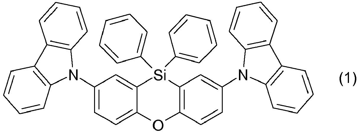

- To a round bottom flask is added PXBr (synthesis example I.1) (2.00 g, 3.93 mmol) carbazole (1.38 g, 8.25 mmol), and sodium-tert-butoxide (1.13 g,11.8 mmol). Dry xylene (80 ml) is added and nitrogen bubbled through the mixture for 1 hour. Then, Pd(OAc)2 (17.6 mg, 79.6 µmol), tri-tert-butylphosphine (73.8 · l, 0.314 mmol) are added and the resultant mixture is vigorously stirred for 5 hours at reflux temperature under N2 flow. The resulting mixture is cooled to room temperature. The precipitate is filtered, and washed with water. The organic layer is separated and dried over anhydrous MgSO4, filtered, and evaporated. The resulting mixture is filtered through silica gel pad (eluent: toluene). The filtrate is evaporated to dryness, poured into hexane to afford a white solid (2.07g:77.4g).
1H-NMR :(400 MHz,CD2Cl2): δ 8.14 (d, J=8.0 Hz, 4H), 7.80 (d, J = 2.8 Hz, 2H), 7.75 (q, J=8.8Hz , 2H), 7.67-7.60 (m, 6H), 7.47-7.37 (m, 14H), 7.30-7.26 (m, 4H)ppm.
EIMS (m/z)=681[M+]
Anal, Calcd for C48H32N2OSi : C, 84.67; H, 4.74;N, 4.11% Found : C, 84.77; H,4.55;N, 4.11% -


- To a round bottom flask is added PXBr (synthesis example I.1) (3.00 g, 5.90 mmol). After nitrogen flow for 1.5 hour, dry tetrahydrofuran (60 ml) is added. The resultant mixture is cooled to - 70 °C, then n-butyllithium (1.6 M, 11.1 ml) is added dropwise. After stirring for 1 hour at -70°C, ether solution (20 ml) of triphenychlorolsilane (5.21 g, 17.7 mmol) is added dropwise. The resultant mixture is stirred at room temperature. The reaction mixture is evaporated, dissolved in toluene (80 ml) and washed with water. The organic layer is separated and dried over anhydrous MgSO4, filtered, and evaporated to dryness. The resulting solid is purified by recrystallization from toluene to afford a white solid. (2.88 g, 56.3%)
1H-NMR(400MHz,THF-d4) : δ 7.96 (s, 2H), 7.62 (d, J=8.2 Hz, 2H), 7.51 (d, J=8.2 Hz, 12H), 7.39-7.24 (m, 30H) ppm,
EIMS(m/z)=868 [M+],
Anal, Calcd for C60H46OSi3: C, 83.09; H, 5.35%. Found: C, 83.04; H, 5.28%. -


- To a round bottom flask is added PXBr (synthesis example I.1) (2.00 g, 3.93 mmol) and dibenzofuran-4-boronic acid (2.43 g, 8.25 mmol). To the mixture are added toluene (40.0 ml), ethanol (20.0 ml) and aqueous Na2CO3 (2.6 M, 11.8 ml) and nitrogen bubbles through the mixture for 1 hour. Then, Pd(PPh)4 (0.23 g, 0.20 mmol) is added and the resultant mixture is vigorously stirred for 12 hours at reflux temperature under N2 flow. The resulting mixture is cooled to room temperature. The precipitate is filtered, and dissolved in reflux toluene (200 ml), filtered through a silica-gel pad. The clear filtrate is evaporated to dryness. The resulting white solid is further purified by recrystallization from toluene (1.45g, 54%).
1H-NMR (400MHz, CD2CI2): δ 8.12 (d, J=2.0Hz, 2H), 8.01 (d, J = 7.6Hz, 2H), 7.86-7.81 (m, 4H), 7.71-7.56 (m, 10H), 7.49-7.34 (m, 12H) ppm.
EIMS (m/z)=683[M+]
Anal, Calcd for C48H32N2OSi: C, 84.43; H, 4.43% Found : C, 84.37; H, 4.21% -


- Compounds (4), (5) and (6) are prepared in analogy to compounds (1), (2) and (3), whereby the correct stoichiometry is to be applied.
-

- Compound (V7) is disclosed in
JP2006083167 - The ITO substrate used as the anode is first cleaned with commercial detergents for LCD production (Deconex® 20NS and 25ORGAN-ACID® neutralizing agent) and then in an acetone/isopropanol mixture in an ultrasound bath. To eliminate possible organic residues, the substrate is exposed to a continuous ozone flow in an ozone oven for a further 25 minutes. This treatment also improves the hole injection properties of the ITO. Next, the AJ20-1000 hole injection layer from Plexcore is spun on from solution (-40 nm).
- Thereafter, the organic materials specified below are applied to the cleaned substrate by vapor deposition at a rate of approx. 0.5-5 nm/min at about 10-8 mbar. The hole conductor and exciton blocker applied to the substrate is Ir(dpbic)3 (V1) (DPBIC) with a thickness of 35 nm doped with MoO3 (-50% by weight) to improve the conductivity.

WO2005/019373
Subsequently, Ir(dpbic)3 (V1) is applied by vapor deposition in a thickness of 5 nm. - Subsequently, a mixture of Emitter (E1) (30% by weight), Ir(dpbic)3 (V1) (host H1) (15% by weight) and compound (1) (synthesis example 1.2) (host H2) (55% by weight) are applied by vapor deposition in a thickness of 40 nm the former compound functioning as an emitter material, the two latter as matrix materials. The weight ratios of E1, H1 and H2 are given below.

WO 2011/073149
Subsequently, the compound (1) is applied by vapor deposition with a thickness of 5 nm as an exciton and hole blocker. - Next, as an electron transporter, a mixture of 50 wt.% (V2) and 50 wt.% Liq in a thickness of 25 nm, a 0.7 nm-thick KF layer and finally a 100 nm-thick Al electrode are applied by vapor deposition. All components are bonded to a glass cover in an inert nitrogen atmosphere.

WO 2006/128800 A1 - As example II.1, except that the host material and the hole blocker material used is compound (2) according to synthesis example 1.3 instead of compound (1).
- As example 11.1, except that the host material and the hole blocker material used is compound (3) according to synthesis example 1.4 instead of compound (1).
- As example II.1, except that the host material and the hole blocker material used is compound (V7) according to synthesis example 1.5 instead of compound (1).
- To characterize the OLEDs of examples II.1, II.2 and II.3 and the OLED of comparative example II.4, electroluminescence spectra are recorded at different currents and voltages. In addition, the current-voltage characteristic is measured in combination with the emitted light output. The light output can be converted to photometric parameters by calibration with a photometer. The data are shown in table 1.
- As example II.1, except that the host material and the hole blocker material used is compound (4), (5) or (6), respectively according to synthesis example 1.5 instead of compound (1).
- The OLEDs (4), (5) and (6) obtained emit blue light.
Table 1 OLED Example (host and hole blocker) CIE-x1) absolute values CIE-y2) absolute values Voltage 300 nits normalized values3) EQE4) 300 nits normalized values3) LD5) 300 nits normalized values3) OLED II.1 (1) 0.177 0.347 0.798 7.683 3.635 OLED II.2 (2) 0.188 0.37 0.691 9.025 34.594 OLED II.3 (3) 0.188 0.381 0.716 7.935 4.421 OLED II.4 (V7) 0.18 0.329 1.000 1.000 1.000 1) CIE (International Commission on Illumination) color coordinate: x-coordinate
2) CIE (International Commission on Illumination) color coordinate: y-coordinate
3) Normalized values: Normalized relative to the values of comparative OLED II.4 (host and hole blocker material: (V7)) - the values of the comparative OLED II.4 (host and hole blocker material: (V7)) are set to 1.000
4) EQE: external quantum efficiency
5) LD: lifetime - The performance of the inventive OLEDs (1) to (3) is clearly superior compared with the performance of the comparative OLED (V7). The only difference between the inventive OLEDs and the comparative OLED is the material employed as host in the light emitting layer and as exciton and hole blocker, which is according to the present invention a phenoxasiline compound and according to the comparative example a phenazasiline compound. The superiority of the inventive phenoxasilines over phenazasilines is especially evident in the following OLED properties:
- i) Voltage: the OLEDs of the present invention comprising the phenoxasilines according to the present invention perform at significantly lower voltage than OLEDs comprising phenazasilines;
- ii) External quantum efficiency (EQE): the OLEDs of the present invention comprising the phenoxasilines according to the present invention show a significantly higher EQE than OLEDs comprising phenazasilines;
- iii) Lifetime (LD): the OLEDs of the present invention comprising the phenoxasilines according to the present invention show a significantly longer lifetime than OLEDs comprising phenazasilines; this is especially clear from the direct comparison of OLED II.2 (host and hole blocker material: (2)) and OLED 11.4 (host and holeblocker material (V7)), wherein the substituents of the phenoxasiline (according to the present invention; (2)) and the phenazasiline (comparative example; (V7)) are identical.
By virtue of the use of the phenoxasiline derivatives of the formula (I) substituted by at least one substituent Y, organic electronics applications, especially OLEDs, organic solar cells and switching elements, preferably OLEDs, with a long lifetime a low driving voltage and a high efficiency are obtained. In addition, in OLEDs having the phenoxasiline derivatives of the formula (I) used in accordance with the invention, problematic aggregation and exciplex formation, which result in loss of efficiency and color purity, are avoided. It is thus possible in accordance with the invention to provide highly effective and pure-color OLEDs with long lifetime or organic solar cells and switching elements with long lifetime.
It has been found that the phenoxasiline derivatives of the formula (I) are particularly suitable for use in applications in which charge carrier transporting and injection performance is required, especially for use in organic electronics applications, for example selected from switching elements such as organic transistors, e.g. organic FETs (field-effect transistors) and organic TFTs (thin-film transistors), organic solar cells and organic light-emitting diodes (OLEDs), the phenoxasiline derivatives of the formula (I) in OLEDs being particularly suitable for use as host (matrix) material, preferably in a light-emitting layer, and/or as electron/hole/exciton transport material and/or as electron/hole/ exciton blocking material and/or as electron/hole/exciton injection material, especially in combination with a phosphorescence emitter or as an organic semiconductor layer.
Even more preferably, Y is selected from the group consisting of

wherein
R13 is H or phenoxasilinyl of formula (I'), preferably H.

wherein


R3' and R4' form together with A3' and A4' an unsaturated ring having a total of from 5 to 18 carbon atoms and/or heteroatoms, which is optionally interrupted by at least one further heteroatom and optionally substituted,
R6' and R7', R7' and R8' or R8' and R9' form together with the C-atoms to which R6', R7', R8' and R9' are linked, an unsaturated ring having a total of from 5 to 18 carbon atoms and/or heteroatoms, which is optionally interrupted by at least one further heteroatom and is optionally substituted,
and/or
if A5' is C, R5' and R6' together form a bridge comprising a total of from 1 to 30 carbon atoms and/or heteroatoms which is optionally annulated with a substituted or unsubstituted five to eight membered carbon atoms and/or heteroatoms comprising ring, which bridge is saturated or unsaturated, linear or branched, optionally comprises heteroatoms, an aromatic unit, a heteroaromatic unit and/or functional groups,
Claims (14)
- Organic electronics applications comprising at least one compound of the formula (I)
 R1, R2, R3, R4, R5, R6 and R7
are each independently hydrogen, C1-C20-alkyl, C3-C20-cycloalkyl, heterocycloalkyl having 3 to 20 ring atoms, C6-C30-aryl, heteroaryl having 5 to 30 ring atoms or a substituent with donor or acceptor action selected from the group consisting of C1-C20-alkoxy, C6-C30- aryloxy, C1-C20-alkylthio, C6-C30-arylthio, SiR10R11R12, halogen radicals, halogenated C1-C20-alkyl radicals, carbonyl (-CO(R10)), carbonylthio (-C=O(SR10)), carbonyloxy (-C=O(OR10)), oxycarbonyl (-OC=O(R10)), thiocarbonyl (-SC=O(R10)), amino (-NR10R11), OH, pseudohalogen radicals, amido (-C=O(NR10)), -NR10C=O(R11), phosphonate (- P(O) (OR10)2), phosphate (-OP(O)(OR10)2), phosphine (-PR10R11), phosphine oxide (-P(O)R10 2), sulfate (-OS(O)2OR10), sulfoxide (-S(O)R10), sulfonate (-S(O)2OR10), sulfonyl (-S(O)2R10), sulfonamide (-S(O)2NR10R11), NO2, boronic esters (-OB(OR10)2), imino (-C=NR10R11), borane radicals, stannane radicals, hydrazine radicals, hydrazone radicals, oxime radicals, nitroso groups, diazo groups, vinyl groups, sulfoximines, alanes, germanes, boroxines and borazines;or two adjacent R1, R2, R3, R4, R5, R6 or R7 radicals, in each case together with the carbon atoms to which they are bonded, form a ring having a total of 3 to 12 atoms, where the ring may be saturated or mono- or polyunsaturated and, as well as carbon atoms, may have one or more heteroatoms selected from N, O and P, where the ring may be unsubstituted or mono- or polysubstituted and/or may be fused to further 3- to 12-membered rings;R8 and R9
are each independently C1-C20-alkyl, C3-C20-cycloalkyl, heterocycloalkyl having 3 to 20 ring atoms, C6-C30-aryl or heteroaryl having 5 to 30 ring atoms;R10, R11, R12
are each independently C1-C20-alkyl, C3-C20-cycloalkyl, heterocycloalkyl having 3 to 20 ring atoms, C6-C30-aryl, heteroaryl having 5 to 30 ring atoms, -O-Si(C1-C20-alkyl)3, -O-Si(C5-C30-aryl)3, C1-C20-alkoxy or C6-C30-aryloxy;or two adjacent R10 and R11, R10 and R12 or R11 and R12 radicals, together with the atom to which they are bonded, form a ring having a total of 3 to 12 atoms, where the ring may be saturated or mono- or polyunsaturated and, as well as the atom to which the R10, R11 or R12 radicals are bonded, may have exclusively carbon atoms or one or more further heteroatoms selected from N, O and P, where the ring may be unsubstituted or mono- or polysubstituted and/or may be fused to further 3- to 12-membered rings;Y is C2-C20-alkyl, C3-C20-cycloalkyl, heterocycloalkyl having 3 to 20 ring atoms, C6-C30-aryl, heteroaryl having 5 to 30 ring atoms or a substituent with donor or acceptor action selected from the group consisting of C1-C20-alkoxy, C6-C30-aryloxy, C1-C20-alkylthio, C6-C30-arylthio, SiR10R11R12, halogen radicals, halogenated C1-C20-alkyl radicals, carbonyl (-CO(R10)), carbonylthio (-C=O(SR10)), carbonyloxy (-C=O(OR10)), oxycarbonyl (-OC= O(R10)), thiocarbonyl (-SC=O(R10)), amino (-NR10R11), OH, pseudohalogen radicals, amido (-C=O(NR10)), -NR10C=O(R11), phosphonate (-P(O)(OR10)2), phosphate (-OP(O) (OR10)2), phosphine (-PR10R11), phosphine oxide (-P(O)R10 2), sulfate (-OS(O)2OR10), sulfoxide (-S(O)R10), sulfonate (-S(O)2OR10), sulfonyl (-S(O)2R10), sulfonamide (-S(O)2NR10R11), NO2, boronic esters (-OB(OR10)2), imino (-C=NR10R11), borane radicals, stannane radicals, hydrazine radicals, hydrazone radicals, oxime radicals, nitroso groups, diazo groups, vinyl groups, sulfoximines, alanes, germanes, boroxines and borazines; preferably heteroaryl having 5 to 30 ring atoms selected from the group consisting of pyrrolyl, furanyl, thienyl, benzoanellated ring systems of pyrrolyl, furanyl, thienyl, for example benzofuranyl, benzothienyl, indolyl, isoindolyl, isoindolizinyl, carbazolyl, azacarbazolyl, diazacarbazolyl, dibenzofuryl, dibenzothienyl, pyridyl, pyrimidyl, pyrazolyl, imidazolyl, thiazolyl, oxazolyl, triazolyl and phenanthrolinyl; or SiR10R11R12. - Organic electronics applications according to claim 1 , wherein
Y is heteroaryl having 5 to 30 ring atoms selected from the group consisting of pyrrolyl, furanyl, thienyl, benzoanellated ring systems of pyrrolyl, furanyl, thienyl, for example benzofuranyl, benzothienyl, indolyl, isoindolyl, isoindolizinyl, carbazolyl, azacarbazolyl, diazacarbazolyl, dibenzofuryl, dibenzothienyl, pyridyl, pyrimidyl, pyrazolyl, imidazolyl, thiazolyl, oxazolyl, triazolyl and phenanthrolinyl; or SiR10R11R12; preferably, Y is selected from the group consisting of pyrrolyl, furanyl, thienyl, benzofuranyl, benzothienyl, indolyl, isoindolyl, isoindolizinyl, carbazolyl, azacarbazolyl, diazacarbazolyl, dibenzofuryl, dibenzothienyl and SiPh3; and
R10, R11 and R12
are each independently C6-C30-aryl, preferably phenyl. - Organic electronics applications according to claim 1 or 2, wherein
Y is selected from the group consisting of

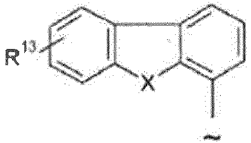
whereinX is NR10, O or S,R10 is C1-C20-alkyl, C3-C20-cycloalkyl, heterocycloalkyl having 3 to 20 ring atoms, C6-C30-aryl, heteroaryl having 5 to 30 ring atoms, -O-Si(C1-C20-alkyl)3, -O-Si(C6-C30-aryl)3, C1-C20-alkoxy or C6-C30-aryloxy; preferably C6-C30-aryl, more preferably phenyl, andR13 is H or phenoxasilinyl of formula (I'), preferably H, and the symbol ∼ means that there is a binding site at the position marked with ∼;preferably, Y is selected from the group consisting of
- Organic electronics applications according to any of claims 1 to 3, wherein
R8 and R9
are each independently C6-C30-aryl or heteroaryl having 5 to 30 ring atoms; preferably, R8 and R9 are each independently phenyl, which is most preferably unsubstituted, dibenzofuranyl or carbazolyl; more preferably, R8 and R9 are each independently unsubstituted phenyl,
R13 is H or phenoxasilinyl of formula (I'), preferably H,
and the symbol ∼ means that there is a binding site at the position marked with ∼. - Organic electronics applications according to any of claims 1 to 4, wherein
R8 and R9 are identical. - Organic electronics applications according to any of claims 1 to 5, wherein R1, R2, R3, R4, R5, R6 and R7 are each hydrogen or R1, R2, R5, R6 and R7 are each hydrogen and R3 and R4 are each independently C1-C20-alkyl, C3-C20-cycloalkyl, heterocycloalkyl having 3 to 20 ring atoms, C6-C30-aryl, heteroaryl having 5 to 30 ring atoms, methoxy, phenyloxy, halogenated C1-C4-alkyl, preferably CF3, CH2F, CHF2, C2F5, halogen, preferably F, CN, SiR10R11R12, P(O)Ph2 or diphenylamino, preferably methyl, phenyl, carbazolyl, dibenzofuryl, methoxy, phenyloxy, CF3, CH2F, CHF2, C2F5, F, CN, SiR10R11R12, P(O)Ph2 or diphenylamino.
- Organic electronics applications according to any of claims 1 to 5, wherein
R1, R2, R3, R4, R5, R6 and R7 are hydrogen, and
R6 is heteroaryl having 5 to 30 ring atoms selected from the group consisting of pyrrolyl, furanyl, thienyl, benzoanellated ring systems of pyrrolyl, furanyl, thienyl, for example benzofuranyl, benzothienyl, indolyl, isoindolyl, isoindolizinyl, carbazolyl, azacarbazolyl, diazacarbazolyl, dibenzofuryl, dibenzothienyl, pyridyl, pyrimidyl, pyrazolyl, imidazolyl, thiazolyl, oxazolyl, triazolyl and phenanthrolinyl; or SiR10R11R12; preferably, R6 is selected from the group consisting of pyrrolyl, furanyl, thienyl, benzofuranyl, benzothienyl, indolyl, isoindolyl, isoindolizinyl, carbazolyl, azacarbazolyl, diazacarbazolyl, dibenzofuryl, dibenzothienyl and SiPh3; and
R10, R11 and R12
are each independently C6-C30-aryl, preferably phenyl;
more preferably,
R6 is selected from the group consisting of


whereinX is NR10, O or S,R10 is C1-C20-alkyl, C3-C20-cycloalkyl, heterocycloalkyl having 3 to 20 ring atoms, C6-C30-aryl, heteroaryl having 5 to 30 ring atoms, -O-Si(C1-C20-alkyl)3, -O-Si(C5-C30-aryl)3, C1-C20-alkoxy or C6-C30-aryloxy; preferably C6-C30-aryl, more preferably phenyl, andR13 is H or phenoxasilinyl of formula (I'), preferably H; and the symbol ∼ means that there is a binding site at the position marked with ∼;even more preferably, R6 is selected from the group consisting of
orR1, R2, R5, R6 and R7 are hydrogen,R3 and R4 are independently C1-C20-alkyl, C3-C20-cycloalkyl, heterocycloalkyl having 3 to 20 ring atoms, C6-C30-aryl, heteroaryl having 5 to 30 ring atoms, methoxy, phenyloxy, halogenated C1-C4-alkyl, preferably CF3, CH2F, CHF2, C2F5, halogen, preferably F, CN, SiR10R11R12, P(O)Ph2 or diphenylamino; preferably methyl, phenyl, carbazolyl, dibenzofuryl, methoxy, phenyloxy, CF3, CH2F, CHF2, C2F5, F, CN, SiR10R11R12, P(O)Ph2 or diphenylamino; andR6 is heteroaryl having 5 to 30 ring atoms selected from the group consisting of pyrrolyl, furanyl, thienyl, benzoanellated ring systems of pyrrolyl, furanyl, thienyl, for example benzofuranyl, benzothienyl, indolyl, isoindolyl, isoindolizinyl, carbazolyl, azacarbazolyl, diazacarbazolyl, dibenzofuryl, dibenzothienyl, pyridyl, pyrimidyl, pyrazolyl, imidazolyl, thiazolyl, oxazolyl, triazolyl and phenanthrolinyl; or SiR10R11R12; preferably, R6 is selected from the group consisting of pyrrolyl, furanyl, thienyl, benzofuranyl, benzothienyl, indolyl, isoindolyl, isoindolizinyl, carbazolyl, azacarbazolyl, diazacarbazolyl, dibenzofuryl, dibenzothienyl and SiPh3; andR10, R11 and R12
are each independently C6-C30-aryl, preferably phenyl;more preferably,R6 is selected from the group consisting of


whereinX is NR10, O or S,R10 is C1-C20-alkyl, C3-C20-cycloalkyl, heterocycloalkyl having 3 to 20 ring atoms, C6-C30-aryl, heteroaryl having 5 to 30 ring atoms, -O-Si(C1-C20-alkyl)3, -O-Si(C6-C30-aryl)3, C1-C20-alkoxy or C6-C30-aryloxy; preferably C6-C30-aryl, more preferably phenyl, andR13 is H or phenoxasilinyl of formula (I'), preferably H; and the symbol ∼ means that there is a binding site at the position marked with ∼;even more preferably, R6 is selected from the group consisting of
- Organic electronics applications according to claim 6 or 7, wherein the compound of formula (I) is selected from the compounds of formulae (Ia), (Ib), (Ic) and (Id)

 Y and R6
are each independently heteroaryl having 5 to 30 ring atoms selected from the group consisting of pyrrolyl, furanyl, thienyl, benzoanellated ring systems of pyrrolyl, furanyl, thienyl, for example benzofuranyl, benzothienyl, indolyl, isoindolyl, isoindolizinyl, carbazolyl, azacarbazolyl, diazacarbazolyl, dibenzofuryl, dibenzothienyl, pyridyl, pyrimidyl, pyrazolyl, imidazolyl, thiazolyl, oxazolyl, triazolyl and phenanthrolinyl; or SiR10R11R12; preferably, R6 is selected from the group consisting of pyrrolyl, furanyl, thienyl, benzofuranyl, benzothienyl, indolyl, isoindolyl, isoindolizinyl, carbazolyl, azacarbazolyl, diazacarbazolyl, dibenzofuryl, dibenzothienyl and SiPh3;R3 and R4
are each independently C1-C20-alkyl, C3-C20-cycloalkyl, heterocycloalkyl having 3 to 20 ring atoms, C6-C30-aryl, heteroaryl having 5 to 30 ring atoms, methoxy, phenyloxy, halogenated C1-C4-alkyl, preferably CF3, CH2F, CHF2, C2F5, halogen, preferably F, CN, SiR10R11R12, P(O)Ph2 or diphenylamino, preferably methyl, phenyl, carbazolyl, dibenzofuryl, methoxy, phenyloxy, CF3, CH2F, CHF2, C2F5, F, CN, SiR10R11R12, P(O)Ph2 or diphenylamino;
andR10, R11 and R12
are each independently C6-C30-aryl, preferably phenyl;more preferably,Y and R6 are each independently selected from the group consisting of


whereinX is NR10, O or S,R10 is C1-C20-alkyl, C6-C30-aryl, heteroaryl having 5 to 30 ring atoms, -O-Si(C1-C20-alkyl)3, -O-Si(C6-C30-aryl)3, C1-C20-alkoxy or C6-C30-aryloxy; preferably C6-C30- aryl, more preferably phenyl, andR13 is H or phenoxasilinyl of formula (I'), preferably H; and the symbol ∼ means that there is a binding site at the position marked with ∼;even more preferably, R6 is selected from the group consisting of
 R8 and R9are each independently C6-C30-aryl or heteroaryl having 5 to 30 ring atoms; preferably, R8 and R9 are each independently phenyl, which is most preferably unsubstituted, dibenzofuranyl or carbazolyl; more preferably, R8 and R9 are each independently unsubstituted phenyl,
- Organic electronics applications according to any of claims 1 to 8, wherein the organic applications are OLEDs.
- The OLED according to claim 9 comprising an anode An and a cathode Ka and a light-emitting layer E arranged between the anode An and the cathode Ka, and optionally at least one further layer selected from the group consisting of at least one blocking layer for holes/excitons, at least one blocking layer for electrons/excitons, at least one hole injection layer, at least one hole conductor layer, at least one electron injection layer and at least one electron conductor layer, wherein the at least one compound of the formula (I) is present in the light-emitting layer E and/or in at least one of the further layers, wherein the at least one compound of the formula (I) is preferably present in the light-emitting layer as a host and/or in the blocking layer for holes/excitons and/or in the hole injection layer.
- Organic electronics applications according to any of claims 1 to 10, wherein the compound of formula (I) is employed as host material, electron/exciton transport material, hole/exciton transport material, hole/exciton blocker material, electron/exciton blocker material, hole/exciton injection material and/or electron/exciton injection material.
- A light-emitting layer, electron/exciton transport layer, hole/exciton transport layer, hole/exciton blocking layer, electron/exciton blocking layer, hole/exciton injection layer and/or electron/exciton injection layer comprising at least one compound of formula (I) as defined in any of claims 1 to 8.
- A device selected from the group consisting of stationary visual display units such as visual display units of computers, televisions, visual display units in printers, kitchen appliances and advertising panels, illuminations, information panels; and mobile visual display units such as visual display units in smartphones, cellphones, laptops, digital cameras, MP3 players, vehicles and destination displays on buses and trains; illumination units; keyboards; garments; furniture or wallpaper comprising at least one organic light-emitting diode as claimed in claims 9 and 10.
- Use of a compound of formula (I) according to any of claims 1 to 8 in organic electronics applications, preferably in OLEDs.
Priority Applications (1)
| Application Number | Priority Date | Filing Date | Title |
|---|---|---|---|
| EP13786274.4A EP2917950B1 (en) | 2012-11-06 | 2013-11-06 | Phenoxasiline based compounds for electronic application |
Applications Claiming Priority (4)
| Application Number | Priority Date | Filing Date | Title |
|---|---|---|---|
| US201261722809P | 2012-11-06 | 2012-11-06 | |
| EP12191408 | 2012-11-06 | ||
| EP13786274.4A EP2917950B1 (en) | 2012-11-06 | 2013-11-06 | Phenoxasiline based compounds for electronic application |
| PCT/EP2013/073120 WO2014072320A1 (en) | 2012-11-06 | 2013-11-06 | Phenoxasiline based compounds for electronic application |
Publications (2)
| Publication Number | Publication Date |
|---|---|
| EP2917950A1 EP2917950A1 (en) | 2015-09-16 |
| EP2917950B1 true EP2917950B1 (en) | 2018-07-18 |
Family
ID=47115613
Family Applications (1)
| Application Number | Title | Priority Date | Filing Date |
|---|---|---|---|
| EP13786274.4A Active EP2917950B1 (en) | 2012-11-06 | 2013-11-06 | Phenoxasiline based compounds for electronic application |
Country Status (7)
| Country | Link |
|---|---|
| US (2) | US10319917B2 (en) |
| EP (1) | EP2917950B1 (en) |
| JP (1) | JP6491099B2 (en) |
| KR (1) | KR102080365B1 (en) |
| CN (1) | CN104904032B (en) |
| TW (1) | TWI597285B (en) |
| WO (1) | WO2014072320A1 (en) |
Families Citing this family (22)
| Publication number | Priority date | Publication date | Assignee | Title |
|---|---|---|---|---|
| RU2670218C2 (en) | 2013-08-05 | 2018-10-19 | Басф Се | Cyanated naphthalenebenzimidazole compounds |
| CN115160373A (en) | 2014-03-31 | 2022-10-11 | Udc 爱尔兰有限责任公司 | Metal complexes and their use in organic light-emitting diodes |
| EP3015469B1 (en) | 2014-10-30 | 2018-12-19 | Idemitsu Kosan Co., Ltd. | 5-(benzimidazol-2-yl)benzimidazo[1,2-a]benzimidazoles for electronic applications |
| EP3061759B1 (en) | 2015-02-24 | 2019-12-25 | Idemitsu Kosan Co., Ltd | Nitrile substituted dibenzofurans |
| EP3072943B1 (en) | 2015-03-26 | 2018-05-02 | Idemitsu Kosan Co., Ltd. | Dibenzofuran/carbazole-substituted benzonitriles |
| WO2018024719A1 (en) * | 2016-08-04 | 2018-02-08 | Merck Patent Gmbh | Formulation of an organic functional material |
| WO2018083169A1 (en) * | 2016-11-04 | 2018-05-11 | Cynora Gmbh | Organic electroluminescent devices comprising host compounds |
| KR102727253B1 (en) * | 2016-11-14 | 2024-11-08 | 삼성디스플레이 주식회사 | Heterocyclic compound and organic electroluminescence device including the same |
| KR102504131B1 (en) | 2017-04-27 | 2023-02-28 | 삼성디스플레이 주식회사 | Heterocyclic compound and organic light emitting device comprising the same |
| KR102389254B1 (en) | 2017-05-16 | 2022-04-22 | 삼성디스플레이 주식회사 | Heterocyclic compound and organic electroluminescence device including the same |
| US11608321B2 (en) * | 2017-06-23 | 2023-03-21 | Universal Display Corporation | Organic electroluminescent materials and devices |
| KR102138410B1 (en) * | 2017-06-30 | 2020-07-27 | 주식회사 엘지화학 | Organic light emitting device |
| KR102405140B1 (en) | 2017-07-12 | 2022-06-08 | 삼성디스플레이 주식회사 | Heterocyclic compound and organic electroluminescence device including the same |
| CN107425042B (en) * | 2017-07-27 | 2020-05-01 | 京东方科技集团股份有限公司 | OLED array substrate and display device |
| KR102436431B1 (en) | 2017-09-21 | 2022-08-29 | 삼성디스플레이 주식회사 | Aromatic compound and organic electroluminescence device including the same |
| EP3598515B1 (en) * | 2018-07-18 | 2024-09-04 | Novaled GmbH | Compound and organic semiconducting layer, organic electronic device, display device and lighting device comprising the same |
| KR102757332B1 (en) * | 2018-07-27 | 2025-01-21 | 삼성디스플레이 주식회사 | Amine compound and organic light emitting device comprising the same |
| CN110204567B (en) * | 2019-06-04 | 2020-12-04 | 武汉华星光电半导体显示技术有限公司 | Organic compound, application thereof and organic light-emitting diode electroluminescent device |
| CN112151682B (en) * | 2019-06-26 | 2023-08-22 | 夏禾科技(江苏)有限公司 | Organic electroluminescent device comprising hole blocking layer and electron transport layer |
| CN113054144A (en) * | 2019-12-28 | 2021-06-29 | Tcl集团股份有限公司 | Nano material and preparation method thereof, quantum dot light-emitting diode and preparation method thereof |
| CN114478607B (en) * | 2021-12-30 | 2024-05-14 | 武汉尚赛光电科技有限公司 | Organic luminescent material, application and device thereof |
| KR102656473B1 (en) * | 2022-11-29 | 2024-04-12 | 엘티소재주식회사 | Composition for organic light-emitting device and organic light-emitting device comprising same |
Family Cites Families (43)
| Publication number | Priority date | Publication date | Assignee | Title |
|---|---|---|---|---|
| KR100913568B1 (en) | 1999-05-13 | 2009-08-26 | 더 트러스티즈 오브 프린스턴 유니버시티 | Very high efficiency organic light emitting devices based on electrophosphorescence |
| WO2001041512A1 (en) | 1999-12-01 | 2001-06-07 | The Trustees Of Princeton University | Complexes of form l2mx as phosphorescent dopants for organic leds |
| JP2001181285A (en) * | 1999-12-24 | 2001-07-03 | Hitachi Chem Co Ltd | Method of producing 10,10-dialkylphenoxasilin-2,3,7,8-tetra- carboxylic acid and its dianhydride and its intermediate |
| US6821645B2 (en) | 1999-12-27 | 2004-11-23 | Fuji Photo Film Co., Ltd. | Light-emitting material comprising orthometalated iridium complex, light-emitting device, high efficiency red light-emitting device, and novel iridium complex |
| US6565994B2 (en) | 2000-02-10 | 2003-05-20 | Fuji Photo Film Co., Ltd. | Light emitting device material comprising iridium complex and light emitting device using same material |
| US20020121638A1 (en) | 2000-06-30 | 2002-09-05 | Vladimir Grushin | Electroluminescent iridium compounds with fluorinated phenylpyridines, phenylpyrimidines, and phenylquinolines and devices made with such compounds |
| US7306856B2 (en) | 2000-07-17 | 2007-12-11 | Fujifilm Corporation | Light-emitting element and iridium complex |
| CN101924190B (en) | 2000-08-11 | 2012-07-04 | 普林斯顿大学理事会 | Organometallic compounds and emission-shifting organic electrophosphorescence |
| JP4344494B2 (en) | 2000-08-24 | 2009-10-14 | 富士フイルム株式会社 | Light emitting device and novel polymer element |
| JP4067286B2 (en) | 2000-09-21 | 2008-03-26 | 富士フイルム株式会社 | Light emitting device and iridium complex |
| JP4154138B2 (en) | 2000-09-26 | 2008-09-24 | キヤノン株式会社 | Light emitting element, display device and metal coordination compound |
| JP4154139B2 (en) | 2000-09-26 | 2008-09-24 | キヤノン株式会社 | Light emitting element |
| KR100867495B1 (en) * | 2000-11-24 | 2008-11-06 | 도레이 가부시끼가이샤 | Luminescent Element Material and Luminescent Element Comprising the Same |
| JP4086499B2 (en) | 2000-11-29 | 2008-05-14 | キヤノン株式会社 | Metal coordination compound, light emitting device and display device |
| JP4154145B2 (en) | 2000-12-01 | 2008-09-24 | キヤノン株式会社 | Metal coordination compound, light emitting device and display device |
| DE10104426A1 (en) | 2001-02-01 | 2002-08-08 | Covion Organic Semiconductors | Process for the production of high-purity, tris-ortho-metallated organo-iridium compounds |
| JP4843889B2 (en) | 2001-09-26 | 2011-12-21 | 東レ株式会社 | Light emitting element |
| JP4048792B2 (en) * | 2002-02-20 | 2008-02-20 | コニカミノルタホールディングス株式会社 | Organic electroluminescence element and display device |
| JP4590825B2 (en) * | 2003-02-21 | 2010-12-01 | コニカミノルタホールディングス株式会社 | White light emitting organic electroluminescence device |
| DE10338550A1 (en) | 2003-08-19 | 2005-03-31 | Basf Ag | Transition metal complexes with carbene ligands as emitters for organic light-emitting diodes (OLEDs) |
| WO2005113704A2 (en) | 2004-05-18 | 2005-12-01 | The University Of Southern California | Luminescent compounds with carbene ligands |
| JP4700442B2 (en) | 2004-08-19 | 2011-06-15 | ケミプロ化成株式会社 | A phenazacillin derivative, a hole transport material comprising the same, a hole injection material, a light emitting layer host material, and an organic EL device including the same. |
| DE102004057072A1 (en) | 2004-11-25 | 2006-06-01 | Basf Ag | Use of Transition Metal Carbene Complexes in Organic Light Emitting Diodes (OLEDs) |
| ATE430789T1 (en) | 2004-12-23 | 2009-05-15 | Ciba Holding Inc | ELECTROLUMINESCENT METAL COMPLEXES WITH NUCLEOPHILIC CARBENE LIGANDS |
| DE102005014284A1 (en) | 2005-03-24 | 2006-09-28 | Basf Ag | Use of compounds containing aromatic or heteroaromatic rings containing groups via carbonyl groups as matrix materials in organic light-emitting diodes |
| TWI418606B (en) | 2005-04-25 | 2013-12-11 | Udc Ireland Ltd | Organic electroluminescent device |
| US8586204B2 (en) | 2007-12-28 | 2013-11-19 | Universal Display Corporation | Phosphorescent emitters and host materials with improved stability |
| US9051344B2 (en) | 2005-05-06 | 2015-06-09 | Universal Display Corporation | Stability OLED materials and devices |
| KR101425423B1 (en) | 2005-05-30 | 2014-08-01 | 시바 홀딩 인크 | Electroluminescent device |
| EP1786050B1 (en) | 2005-11-10 | 2010-06-23 | Novaled AG | Doped organic semiconductor material |
| CN101415718B (en) | 2006-02-10 | 2013-05-29 | 通用显示公司 | Cyclometallated imidazo[1,2-f]phenanthridine and diimidazo[1,2-a:1',2'-c]quinazoline ligands and their isoelectronic and benzocyclization analogs metal complexes |
| EP1837926B1 (en) | 2006-03-21 | 2008-05-07 | Novaled AG | Heterocyclic radicals or diradicals and their dimers, oligomers, polymers, di-spiro and polycyclic derivatives as well as their use in organic semiconductor materials and electronic devices. |
| CN103880891A (en) | 2006-04-04 | 2014-06-25 | 巴斯夫欧洲公司 | Transition metal complexes comprising one noncarbene ligand and one or two carbene ligands and their use in oleds |
| ATE550342T1 (en) | 2006-04-05 | 2012-04-15 | Basf Se | HETEROLEPTIC TRANSITION METAL-CARBEN COMPLEXES AND THEIR USE IN ORGANIC LIGHT-LIGHT DIODES (OLEDS) |
| JP2009541431A (en) | 2006-06-26 | 2009-11-26 | ビーエーエスエフ ソシエタス・ヨーロピア | Use of transition metal-carbene complexes without cyclometalation via non-carbene |
| CN101542770B (en) | 2006-09-21 | 2012-05-30 | 巴斯夫欧洲公司 | OLED display with extended lifetime |
| CN101687349A (en) | 2007-06-28 | 2010-03-31 | 巴斯夫欧洲公司 | Moulded foams made of expandable acrylonitrile copolymers |
| JP5804703B2 (en) | 2007-07-05 | 2015-11-04 | ビーエーエスエフ ソシエタス・ヨーロピアBasf Se | Organic light emitting diode comprising at least one disilyl compound selected from disilylcarbazole, disilyldibenzofuran, disilyldibenzothiophene, disilyldibenzophosphole, disilyldibenzothiophene S-oxide and disilyldibenzothiophene S, S-dioxide |
| US9487548B2 (en) | 2009-12-14 | 2016-11-08 | Udc Ireland Limited | Metal complexes comprising diazabenzimidazolocarbene ligands and the use thereof in OLEDs |
| US8691401B2 (en) | 2010-04-16 | 2014-04-08 | Basf Se | Bridged benzimidazole-carbene complexes and use thereof in OLEDS |
| US8883322B2 (en) | 2011-03-08 | 2014-11-11 | Universal Display Corporation | Pyridyl carbene phosphorescent emitters |
| KR102029336B1 (en) * | 2012-08-21 | 2019-10-07 | 제일모직 주식회사 | Compound for organic optoelectronic device, organic light emitting diode including the same and display including the organic light emitting diode |
| JP6023635B2 (en) * | 2013-04-15 | 2016-11-09 | 出光興産株式会社 | Fused ring amine compound and organic electroluminescence device using the same |
-
2013
- 2013-11-06 JP JP2015540169A patent/JP6491099B2/en active Active
- 2013-11-06 CN CN201380069401.6A patent/CN104904032B/en active Active
- 2013-11-06 EP EP13786274.4A patent/EP2917950B1/en active Active
- 2013-11-06 US US14/440,637 patent/US10319917B2/en active Active
- 2013-11-06 TW TW102140337A patent/TWI597285B/en active
- 2013-11-06 WO PCT/EP2013/073120 patent/WO2014072320A1/en not_active Ceased
- 2013-11-06 KR KR1020157014738A patent/KR102080365B1/en active Active
-
2019
- 2019-04-23 US US16/391,608 patent/US11031559B2/en active Active
Non-Patent Citations (1)
| Title |
|---|
| None * |
Also Published As
| Publication number | Publication date |
|---|---|
| US10319917B2 (en) | 2019-06-11 |
| CN104904032B (en) | 2017-08-18 |
| US11031559B2 (en) | 2021-06-08 |
| KR20150079960A (en) | 2015-07-08 |
| TWI597285B (en) | 2017-09-01 |
| US20150318501A1 (en) | 2015-11-05 |
| CN104904032A (en) | 2015-09-09 |
| JP6491099B2 (en) | 2019-03-27 |
| TW201420591A (en) | 2014-06-01 |
| WO2014072320A1 (en) | 2014-05-15 |
| US20190252620A1 (en) | 2019-08-15 |
| JP2016504754A (en) | 2016-02-12 |
| KR102080365B1 (en) | 2020-02-21 |
| EP2917950A1 (en) | 2015-09-16 |
Similar Documents
| Publication | Publication Date | Title |
|---|---|---|
| US11031559B2 (en) | Phenoxasiline based compounds for electronic application | |
| EP2556075B1 (en) | Substituted carbazole derivatives and use thereof in organic electronics | |
| KR101929837B1 (en) | Siloles substituted with condensed ring systems and use thereof in organic electronics | |
| US8637857B2 (en) | Substituted carbazole derivatives and use thereof in organic electronics | |
| EP3016960B1 (en) | Monosubstituted diazabenzimidazole carbene metal complexes for use in organic light emitting diodes | |
| CN107698622B (en) | Organic electronic devices comprising layers comprising at least one metal organic compound and at least one metal oxide | |
| TWI558718B (en) | Material for organic electroluminescent element and organic electroluminescent element using same | |
| CN104471734B (en) | Organic electric-field light-emitting element | |
| US9142792B2 (en) | Organic electronic devices comprising a layer comprising at least one metal organic compound and at least one metal oxide | |
| CN102947416A (en) | Organic electronic devices comprising a layer of a dibenzofurane compound and a 8-hydroxyquinolinolato earth alkaline metal, or alkali metal complex |
Legal Events
| Date | Code | Title | Description |
|---|---|---|---|
| PUAI | Public reference made under article 153(3) epc to a published international application that has entered the european phase |
Free format text: ORIGINAL CODE: 0009012 |
|
| 17P | Request for examination filed |
Effective date: 20150608 |
|
| AK | Designated contracting states |
Kind code of ref document: A1 Designated state(s): AL AT BE BG CH CY CZ DE DK EE ES FI FR GB GR HR HU IE IS IT LI LT LU LV MC MK MT NL NO PL PT RO RS SE SI SK SM TR |
|
| AX | Request for extension of the european patent |
Extension state: BA ME |
|
| DAX | Request for extension of the european patent (deleted) | ||
| 18W | Application withdrawn |
Effective date: 20160713 |
|
| D18W | Application withdrawn (deleted) | ||
| RAP1 | Party data changed (applicant data changed or rights of an application transferred) |
Owner name: UDC IRELAND LIMITED |
|
| STAA | Information on the status of an ep patent application or granted ep patent |
Free format text: STATUS: EXAMINATION IS IN PROGRESS |
|
| 17Q | First examination report despatched |
Effective date: 20170301 |
|
| GRAP | Despatch of communication of intention to grant a patent |
Free format text: ORIGINAL CODE: EPIDOSNIGR1 |
|
| STAA | Information on the status of an ep patent application or granted ep patent |
Free format text: STATUS: GRANT OF PATENT IS INTENDED |
|
| INTG | Intention to grant announced |
Effective date: 20170727 |
|
| GRAJ | Information related to disapproval of communication of intention to grant by the applicant or resumption of examination proceedings by the epo deleted |
Free format text: ORIGINAL CODE: EPIDOSDIGR1 |
|
| STAA | Information on the status of an ep patent application or granted ep patent |
Free format text: STATUS: EXAMINATION IS IN PROGRESS |
|
| GRAP | Despatch of communication of intention to grant a patent |
Free format text: ORIGINAL CODE: EPIDOSNIGR1 |
|
| STAA | Information on the status of an ep patent application or granted ep patent |
Free format text: STATUS: GRANT OF PATENT IS INTENDED |
|
| INTC | Intention to grant announced (deleted) | ||
| INTG | Intention to grant announced |
Effective date: 20180206 |
|
| GRAS | Grant fee paid |
Free format text: ORIGINAL CODE: EPIDOSNIGR3 |
|
| GRAA | (expected) grant |
Free format text: ORIGINAL CODE: 0009210 |
|
| STAA | Information on the status of an ep patent application or granted ep patent |
Free format text: STATUS: THE PATENT HAS BEEN GRANTED |
|
| AK | Designated contracting states |
Kind code of ref document: B1 Designated state(s): AL AT BE BG CH CY CZ DE DK EE ES FI FR GB GR HR HU IE IS IT LI LT LU LV MC MK MT NL NO PL PT RO RS SE SI SK SM TR |
|
| REG | Reference to a national code |
Ref country code: CH Ref legal event code: EP |
|
| REG | Reference to a national code |
Ref country code: IE Ref legal event code: FG4D |
|
| REG | Reference to a national code |
Ref country code: DE Ref legal event code: R096 Ref document number: 602013040533 Country of ref document: DE |
|
| REG | Reference to a national code |
Ref country code: AT Ref legal event code: REF Ref document number: 1020297 Country of ref document: AT Kind code of ref document: T Effective date: 20180815 |
|
| REG | Reference to a national code |
Ref country code: NL Ref legal event code: MP Effective date: 20180718 |
|
| REG | Reference to a national code |
Ref country code: LT Ref legal event code: MG4D |
|
| REG | Reference to a national code |
Ref country code: AT Ref legal event code: MK05 Ref document number: 1020297 Country of ref document: AT Kind code of ref document: T Effective date: 20180718 |
|
| PG25 | Lapsed in a contracting state [announced via postgrant information from national office to epo] |
Ref country code: NL Free format text: LAPSE BECAUSE OF FAILURE TO SUBMIT A TRANSLATION OF THE DESCRIPTION OR TO PAY THE FEE WITHIN THE PRESCRIBED TIME-LIMIT Effective date: 20180718 |
|
| PG25 | Lapsed in a contracting state [announced via postgrant information from national office to epo] |
Ref country code: AT Free format text: LAPSE BECAUSE OF FAILURE TO SUBMIT A TRANSLATION OF THE DESCRIPTION OR TO PAY THE FEE WITHIN THE PRESCRIBED TIME-LIMIT Effective date: 20180718 Ref country code: SE Free format text: LAPSE BECAUSE OF FAILURE TO SUBMIT A TRANSLATION OF THE DESCRIPTION OR TO PAY THE FEE WITHIN THE PRESCRIBED TIME-LIMIT Effective date: 20180718 Ref country code: BG Free format text: LAPSE BECAUSE OF FAILURE TO SUBMIT A TRANSLATION OF THE DESCRIPTION OR TO PAY THE FEE WITHIN THE PRESCRIBED TIME-LIMIT Effective date: 20181018 Ref country code: IS Free format text: LAPSE BECAUSE OF FAILURE TO SUBMIT A TRANSLATION OF THE DESCRIPTION OR TO PAY THE FEE WITHIN THE PRESCRIBED TIME-LIMIT Effective date: 20181118 Ref country code: PL Free format text: LAPSE BECAUSE OF FAILURE TO SUBMIT A TRANSLATION OF THE DESCRIPTION OR TO PAY THE FEE WITHIN THE PRESCRIBED TIME-LIMIT Effective date: 20180718 Ref country code: GR Free format text: LAPSE BECAUSE OF FAILURE TO SUBMIT A TRANSLATION OF THE DESCRIPTION OR TO PAY THE FEE WITHIN THE PRESCRIBED TIME-LIMIT Effective date: 20181019 Ref country code: NO Free format text: LAPSE BECAUSE OF FAILURE TO SUBMIT A TRANSLATION OF THE DESCRIPTION OR TO PAY THE FEE WITHIN THE PRESCRIBED TIME-LIMIT Effective date: 20181018 Ref country code: LT Free format text: LAPSE BECAUSE OF FAILURE TO SUBMIT A TRANSLATION OF THE DESCRIPTION OR TO PAY THE FEE WITHIN THE PRESCRIBED TIME-LIMIT Effective date: 20180718 Ref country code: RS Free format text: LAPSE BECAUSE OF FAILURE TO SUBMIT A TRANSLATION OF THE DESCRIPTION OR TO PAY THE FEE WITHIN THE PRESCRIBED TIME-LIMIT Effective date: 20180718 Ref country code: FI Free format text: LAPSE BECAUSE OF FAILURE TO SUBMIT A TRANSLATION OF THE DESCRIPTION OR TO PAY THE FEE WITHIN THE PRESCRIBED TIME-LIMIT Effective date: 20180718 |
|
| PG25 | Lapsed in a contracting state [announced via postgrant information from national office to epo] |
Ref country code: LV Free format text: LAPSE BECAUSE OF FAILURE TO SUBMIT A TRANSLATION OF THE DESCRIPTION OR TO PAY THE FEE WITHIN THE PRESCRIBED TIME-LIMIT Effective date: 20180718 Ref country code: AL Free format text: LAPSE BECAUSE OF FAILURE TO SUBMIT A TRANSLATION OF THE DESCRIPTION OR TO PAY THE FEE WITHIN THE PRESCRIBED TIME-LIMIT Effective date: 20180718 Ref country code: HR Free format text: LAPSE BECAUSE OF FAILURE TO SUBMIT A TRANSLATION OF THE DESCRIPTION OR TO PAY THE FEE WITHIN THE PRESCRIBED TIME-LIMIT Effective date: 20180718 |
|
| REG | Reference to a national code |
Ref country code: DE Ref legal event code: R097 Ref document number: 602013040533 Country of ref document: DE |
|
| PG25 | Lapsed in a contracting state [announced via postgrant information from national office to epo] |
Ref country code: IT Free format text: LAPSE BECAUSE OF FAILURE TO SUBMIT A TRANSLATION OF THE DESCRIPTION OR TO PAY THE FEE WITHIN THE PRESCRIBED TIME-LIMIT Effective date: 20180718 Ref country code: EE Free format text: LAPSE BECAUSE OF FAILURE TO SUBMIT A TRANSLATION OF THE DESCRIPTION OR TO PAY THE FEE WITHIN THE PRESCRIBED TIME-LIMIT Effective date: 20180718 Ref country code: CZ Free format text: LAPSE BECAUSE OF FAILURE TO SUBMIT A TRANSLATION OF THE DESCRIPTION OR TO PAY THE FEE WITHIN THE PRESCRIBED TIME-LIMIT Effective date: 20180718 Ref country code: ES Free format text: LAPSE BECAUSE OF FAILURE TO SUBMIT A TRANSLATION OF THE DESCRIPTION OR TO PAY THE FEE WITHIN THE PRESCRIBED TIME-LIMIT Effective date: 20180718 |
|
| PLBE | No opposition filed within time limit |
Free format text: ORIGINAL CODE: 0009261 |
|
| STAA | Information on the status of an ep patent application or granted ep patent |
Free format text: STATUS: NO OPPOSITION FILED WITHIN TIME LIMIT |
|
| PG25 | Lapsed in a contracting state [announced via postgrant information from national office to epo] |
Ref country code: SK Free format text: LAPSE BECAUSE OF FAILURE TO SUBMIT A TRANSLATION OF THE DESCRIPTION OR TO PAY THE FEE WITHIN THE PRESCRIBED TIME-LIMIT Effective date: 20180718 Ref country code: SM Free format text: LAPSE BECAUSE OF FAILURE TO SUBMIT A TRANSLATION OF THE DESCRIPTION OR TO PAY THE FEE WITHIN THE PRESCRIBED TIME-LIMIT Effective date: 20180718 Ref country code: DK Free format text: LAPSE BECAUSE OF FAILURE TO SUBMIT A TRANSLATION OF THE DESCRIPTION OR TO PAY THE FEE WITHIN THE PRESCRIBED TIME-LIMIT Effective date: 20180718 |
|
| 26N | No opposition filed |
Effective date: 20190423 |
|
| REG | Reference to a national code |
Ref country code: CH Ref legal event code: PL |
|
| GBPC | Gb: european patent ceased through non-payment of renewal fee |
Effective date: 20181106 |
|
| PG25 | Lapsed in a contracting state [announced via postgrant information from national office to epo] |
Ref country code: LU Free format text: LAPSE BECAUSE OF NON-PAYMENT OF DUE FEES Effective date: 20181106 Ref country code: MC Free format text: LAPSE BECAUSE OF FAILURE TO SUBMIT A TRANSLATION OF THE DESCRIPTION OR TO PAY THE FEE WITHIN THE PRESCRIBED TIME-LIMIT Effective date: 20180718 |
|
| REG | Reference to a national code |
Ref country code: BE Ref legal event code: MM Effective date: 20181130 |
|
| REG | Reference to a national code |
Ref country code: IE Ref legal event code: MM4A |
|
| PG25 | Lapsed in a contracting state [announced via postgrant information from national office to epo] |
Ref country code: LI Free format text: LAPSE BECAUSE OF NON-PAYMENT OF DUE FEES Effective date: 20181130 Ref country code: SI Free format text: LAPSE BECAUSE OF FAILURE TO SUBMIT A TRANSLATION OF THE DESCRIPTION OR TO PAY THE FEE WITHIN THE PRESCRIBED TIME-LIMIT Effective date: 20180718 Ref country code: CH Free format text: LAPSE BECAUSE OF NON-PAYMENT OF DUE FEES Effective date: 20181130 |
|
| PG25 | Lapsed in a contracting state [announced via postgrant information from national office to epo] |
Ref country code: IE Free format text: LAPSE BECAUSE OF NON-PAYMENT OF DUE FEES Effective date: 20181106 Ref country code: FR Free format text: LAPSE BECAUSE OF NON-PAYMENT OF DUE FEES Effective date: 20181130 |
|
| PG25 | Lapsed in a contracting state [announced via postgrant information from national office to epo] |
Ref country code: BE Free format text: LAPSE BECAUSE OF NON-PAYMENT OF DUE FEES Effective date: 20181130 |
|
| PG25 | Lapsed in a contracting state [announced via postgrant information from national office to epo] |
Ref country code: GB Free format text: LAPSE BECAUSE OF NON-PAYMENT OF DUE FEES Effective date: 20181106 |
|
| PG25 | Lapsed in a contracting state [announced via postgrant information from national office to epo] |
Ref country code: MT Free format text: LAPSE BECAUSE OF NON-PAYMENT OF DUE FEES Effective date: 20181106 |
|
| PG25 | Lapsed in a contracting state [announced via postgrant information from national office to epo] |
Ref country code: TR Free format text: LAPSE BECAUSE OF FAILURE TO SUBMIT A TRANSLATION OF THE DESCRIPTION OR TO PAY THE FEE WITHIN THE PRESCRIBED TIME-LIMIT Effective date: 20180718 |
|
| PG25 | Lapsed in a contracting state [announced via postgrant information from national office to epo] |
Ref country code: PT Free format text: LAPSE BECAUSE OF FAILURE TO SUBMIT A TRANSLATION OF THE DESCRIPTION OR TO PAY THE FEE WITHIN THE PRESCRIBED TIME-LIMIT Effective date: 20180718 |
|
| PG25 | Lapsed in a contracting state [announced via postgrant information from national office to epo] |
Ref country code: HU Free format text: LAPSE BECAUSE OF FAILURE TO SUBMIT A TRANSLATION OF THE DESCRIPTION OR TO PAY THE FEE WITHIN THE PRESCRIBED TIME-LIMIT; INVALID AB INITIO Effective date: 20131106 Ref country code: CY Free format text: LAPSE BECAUSE OF FAILURE TO SUBMIT A TRANSLATION OF THE DESCRIPTION OR TO PAY THE FEE WITHIN THE PRESCRIBED TIME-LIMIT Effective date: 20180718 Ref country code: RO Free format text: LAPSE BECAUSE OF FAILURE TO SUBMIT A TRANSLATION OF THE DESCRIPTION OR TO PAY THE FEE WITHIN THE PRESCRIBED TIME-LIMIT Effective date: 20180718 Ref country code: MK Free format text: LAPSE BECAUSE OF NON-PAYMENT OF DUE FEES Effective date: 20180718 |
|
| REG | Reference to a national code |
Ref country code: DE Ref legal event code: R079 Ref document number: 602013040533 Country of ref document: DE Free format text: PREVIOUS MAIN CLASS: H01L0051540000 Ipc: H10K0085000000 |
|
| P01 | Opt-out of the competence of the unified patent court (upc) registered |
Effective date: 20230423 |
|
| PGFP | Annual fee paid to national office [announced via postgrant information from national office to epo] |
Ref country code: DE Payment date: 20251128 Year of fee payment: 13 |