EP2917841B1 - Self track scheme for multi frequency band serializer de-serializer i/o circuits - Google Patents
Self track scheme for multi frequency band serializer de-serializer i/o circuits Download PDFInfo
- Publication number
- EP2917841B1 EP2917841B1 EP13854083.6A EP13854083A EP2917841B1 EP 2917841 B1 EP2917841 B1 EP 2917841B1 EP 13854083 A EP13854083 A EP 13854083A EP 2917841 B1 EP2917841 B1 EP 2917841B1
- Authority
- EP
- European Patent Office
- Prior art keywords
- serializer
- digital data
- signals
- data
- track
- Prior art date
- Legal status (The legal status is an assumption and is not a legal conclusion. Google has not performed a legal analysis and makes no representation as to the accuracy of the status listed.)
- Active
Links
Images
Classifications
-
- H—ELECTRICITY
- H04—ELECTRIC COMMUNICATION TECHNIQUE
- H04L—TRANSMISSION OF DIGITAL INFORMATION, e.g. TELEGRAPHIC COMMUNICATION
- H04L27/00—Modulated-carrier systems
- H04L27/32—Carrier systems characterised by combinations of two or more of the types covered by groups H04L27/02, H04L27/10, H04L27/18 or H04L27/26
- H04L27/34—Amplitude- and phase-modulated carrier systems, e.g. quadrature-amplitude modulated carrier systems
- H04L27/38—Demodulator circuits; Receiver circuits
-
- G—PHYSICS
- G06—COMPUTING OR CALCULATING; COUNTING
- G06F—ELECTRIC DIGITAL DATA PROCESSING
- G06F13/00—Interconnection of, or transfer of information or other signals between, memories, input/output devices or central processing units
- G06F13/38—Information transfer, e.g. on bus
- G06F13/40—Bus structure
- G06F13/4004—Coupling between buses
- G06F13/4027—Coupling between buses using bus bridges
- G06F13/405—Coupling between buses using bus bridges where the bridge performs a synchronising function
- G06F13/4059—Coupling between buses using bus bridges where the bridge performs a synchronising function where the synchronisation uses buffers, e.g. for speed matching between buses
-
- G—PHYSICS
- G06—COMPUTING OR CALCULATING; COUNTING
- G06F—ELECTRIC DIGITAL DATA PROCESSING
- G06F13/00—Interconnection of, or transfer of information or other signals between, memories, input/output devices or central processing units
- G06F13/38—Information transfer, e.g. on bus
- G06F13/40—Bus structure
- G06F13/4063—Device-to-bus coupling
- G06F13/4068—Electrical coupling
- G06F13/4072—Drivers or receivers
-
- G—PHYSICS
- G06—COMPUTING OR CALCULATING; COUNTING
- G06F—ELECTRIC DIGITAL DATA PROCESSING
- G06F13/00—Interconnection of, or transfer of information or other signals between, memories, input/output devices or central processing units
- G06F13/38—Information transfer, e.g. on bus
- G06F13/42—Bus transfer protocol, e.g. handshake; Synchronisation
- G06F13/4265—Bus transfer protocol, e.g. handshake; Synchronisation on a point to point bus
- G06F13/4278—Bus transfer protocol, e.g. handshake; Synchronisation on a point to point bus using an embedded synchronisation
-
- G—PHYSICS
- G06—COMPUTING OR CALCULATING; COUNTING
- G06F—ELECTRIC DIGITAL DATA PROCESSING
- G06F5/00—Methods or arrangements for data conversion without changing the order or content of the data handled
- G06F5/06—Methods or arrangements for data conversion without changing the order or content of the data handled for changing the speed of data flow, i.e. speed regularising or timing, e.g. delay lines, FIFO buffers; over- or underrun control therefor
- G06F5/16—Multiplexed systems, i.e. using two or more similar devices which are alternately accessed for enqueue and dequeue operations, e.g. ping-pong buffers
-
- H—ELECTRICITY
- H04—ELECTRIC COMMUNICATION TECHNIQUE
- H04L—TRANSMISSION OF DIGITAL INFORMATION, e.g. TELEGRAPHIC COMMUNICATION
- H04L27/00—Modulated-carrier systems
- H04L27/32—Carrier systems characterised by combinations of two or more of the types covered by groups H04L27/02, H04L27/10, H04L27/18 or H04L27/26
- H04L27/34—Amplitude- and phase-modulated carrier systems, e.g. quadrature-amplitude modulated carrier systems
- H04L27/36—Modulator circuits; Transmitter circuits
- H04L27/362—Modulation using more than one carrier, e.g. with quadrature carriers, separately amplitude modulated
- H04L27/364—Arrangements for overcoming imperfections in the modulator, e.g. quadrature error or unbalanced I and Q levels
Definitions
- This invention pertains generally to chip-to-chip communications, and more particularly to a self tracking serializer de-serializer.
- serializer de-serializer I/O is based on multiplexing and demultiplexing digital communications. Using such conventional schemes to increase communications bandwidth requires increasing clock rate.
- base band processing techniques can in some cases provide for reliable data transmission and reception, yet it comes with a high cost penalty regarding circuit complexity and unnecessarily long delays for data processing.
- the typical multi-frequency approach may be suitable for high throughput operations, it is not well suited when short latencies are required to perform mission critical operations.
- the present invention fulfills these needs, and overcomes shortcomings of previous multi-frequency chip-to-chip communication topologies.
- US4888792 discloses a multi-level quadrature amplitude modulation and demodulation system that includes a first exchange circuit for cyclicly exchanging input digital signals and for outputting exchanged signals to D/A converters.
- the D/A converters provide analog signals to a QAM modulator which produces a modulated signal.
- a QAM demodulator demodulates the modulated signal to produce analog signals which are converted to digital exchanged signals by A/D converters.
- the digital exchanged signals are exchanged in a manner which is the reverse of that of the first exchange circuit to provide output digital signals on output terminals which respectively correspond to the input terminals.
- This invention concerns an apparatus and method for serializing and de-serializing chip-to-chip communications as defined in the independent claims 1 and 6.
- a chip-to-chip serializer and de-serializer are described which utilize a self tracking method based on track pulse generation on the transmitter (TX) and track pulse restoration on the receiver (RX).
- the data to be transmitted is synchronized with the generated track pulse on TX, with the transmitted data and track pulse being modulated at the same time in the TX.
- All signals communicated chip-to-chip utilizing the present invention are processed under the same conditions, including silicon process variation, power noise, critical path delay, and so forth, thus eliminating/reducing the impact of these variables on operation of the serializer de-serializer.
- the signals are serialized, modulated and transmitted through a short I/O connection from transmitter (TX) to receiver (RX).
- the RX also demodulates all signals under the same conditions and characteristics of the receiver.
- the track pulse is restored in the RX after demodulation. Because the data and track pulse are synchronized in the TX, the signals should likewise be synchronized in the RX when all signals are processed with identical demodulation.
- the self track scheme can sample the restored data at the correct timing. The sample timing tracks the external factors even under different operating conditions, use of different integrated circuit chips or different process technology.
- the next level of synchronization with the system bus after the signal is sampled in the analog-to-digital converter (ADC) which can also be processed based on the timing of restored track pulse.
- ADC analog-to-digital converter
- the restored track pulse can experience significant jitter in practice.
- the implementation provides an improved large jitter tolerance.
- the inventive self tracking serializer de-serializer provides significant improvements to the yield of chip-to-chip I/O circuits.
- the inventive system can be ported to fabricate devices compatible with future silicon process advancements, such as from 28 nm nodes to 14 or 20 nm nodes with minor effort.
- a self tracking serializer de-serializer is described in which a track pulse is generated which travels along with the digital data through serialization and modulation at the transmitter (i.e., first chip) and the demodulation and de-serialization at the receiver (i.e., second chip).
- This self tracking ability allows one to build a circuit with minimum timing overhead without complicated base band processing, while performance and device yield are achieved with low circuit overhead.
- Integrated circuits can be fabricated using this self track mechanism in any desired device technology or process, including 28 nm or use of advanced silicon process technologies.
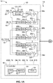
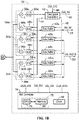
- FIG. 1A and FIG. 1B illustrate an example embodiment 10 for a self tracking multi-frequency band serializer and de-serializer, shown for communicating between a transmitter (TX) in a first chip 12 seen in FIG. 1A over an I/O channel 14, to a receiver (RX) in a second chip 16 seen in FIG. 1B .
- TX transmitter
- RX receiver
- Digital data 18 (DQ_TX) and byte mask 19 (DM_TX) is seen received in the TX in FIG. 1A .
- the byte mask is utilized when the data word to be communicated is sent in multiple sections (e.g., 16 bits over the 8 bit path shown in FIG. 1A , FIG. 1B ).
- the example embodiment often describes a structure allowing sending of 8 bits of digital data (e.g., [7:0])
- the present invention can be configured with any desired number of bits (e.g., 16 bits, 32 bits, and so forth). However, this requires adding more data buffers, converters (DAC, ADC), and modulators and demodulators operating at more frequencies or with higher order encoding.
- the transmitter controller asserts a synchronization signal 20 (DQS_TX) flag to trigger tracking and serialization.
- DQS_TX synchronization signal 20
- the DQS_TX pulse traverses the whole propagation path to which the data is subject.
- a track pulse generator 24 receives synchronization signal 20 (DQS_TX) and a clock signal 22.
- the track pulse generator is configured to generate a synchronized pulse as the flag for data synchronization. It is shown in the figure that DQS_TX is also applied to a buffer for data mask (DM_TX) 19 and as a first input of the data buffers 26a, 26b, 26c, on through to 26m and 26n, which also receive bits within data DQ_TX 18 so that data synchronizes with the track pulse.
- DM_TX buffer for data mask
- the track pulse and digital data word are serialized and modulated for transmission to the receiver.
- Each of these modulators is configured for converting the digital data to analog data which is encoded over multiple frequency channels, such as using multiple modulators which are each configured for operation at a different frequency (e.g., different carrier frequencies). It should be appreciated that one of these modulation frequencies can be zero, that is DC. Using DC as one modulation frequency can reduce the number of frequency generation circuits needed, including phase-locking circuits (e.g., PLL) which are needed.
- phase-locking circuits e.g., PLL
- each modulator utilizes quadrature amplitude modulation (QAM) (e.g., QAM16) and has mixers which encode both an I channel and a Q channel of information into a given modulation frequency.
- QAM quadrature amplitude modulation
- QAM is an analog modulation mechanism, which differs from digital multiplexing used in a digital serialization scheme.
- analog QAM two analog message signals are communicated on each frequency channel by changing (modulating) two carrier waves.
- the two carrier waves typically sinusoids
- the two carrier waves are out of phase with each other by 90° and are thus called quadrature carriers.
- Output over a frequency channel is the sum of the modulated waves of phase modulation (PM) and amplitude modulation (AM).
- PM phase modulation
- AM amplitude modulation
- the internal circuitry for analog QAM is not described. It will be noted that a large number of QAM circuits are available and the technology is well known to one of ordinary skill in the art.
- QAM QAM8/AM16
- QAM32 QAM32
- QAM64 QAM128, and QAM256
- QAM256 QAM256
- PWM pulse-width modulation
- FSK frequency-shift keying
- DAC digital-to-analog converter
- each of the DACs is shown comprising a 2 bit DAC. It should be appreciated, however, that embodiments can be readily implemented using DACs with a different number of bits, such as 4 or more bits.
- Each of the modulators 28a, 28b through 28n operate at a different frequency, with the output of each being summed at the I/O channel 14 and thus travel through the same I/O connection for receipt at second chip 16. This configuration assures a close tracking of the data path through the same modulation process as the tracking signal, regardless of the various channel conditions of I/O channel 14.
- each demodulator receives the incoming analog signal at two mixers (e.g., 36a and 36b, 36c and 36d, on through to 36m and 36n) which also receives 90 degree out-of-phase modulation carriers f i and f q , respectively.
- Demodulated output from each of the mixers is received by analog-to-digital converters (ADC) 38a, 38b through 38m, 38n.
- ADC analog-to-digital converters
- a track pulse restore circuit 40 which operates in combination with output data buffers 42a, 42b, 42c, through 42m and 42n.
- a first output 44 comprises the restored track pulse itself used to synchronize the output from the ADCs to the data buffers.
- Track pulse restore circuit 40 receives a clock 46 (CLK_SYS), and outputs a synchronization signal (pulse) 48 for controlling the latching of data from the ADCs at each of the data buffers whose output is de-serialized digital data (DQ_RX) 52.
- the track pulse restoration circuit sets a flag DQS_RX 50, signaling that the receiver controller can now read the DQ_RX data word.
- a byte mask (DM_RX) 51 is also generated for masking purposes when handling multiple bytes.
- the above serializer and de-serializer are particularly well-suited for operation on a first chip and a second chip between which communication is to be established. It will be appreciated that a second I/O channel can be utilized for establishing a communication path in the opposite direction between the first and second chips.
- This first and second chips seen in FIG. 1A and FIG. 1B are each configured with a controller 62, 74, respectively, for controlling the transmit and receive side operations and generating the signals for operating the serializer and de-serializer.
- the TX controller is shown having at least one processor circuit 64, comprising CPU 68 with memory 70, and utilizing a clock circuit 66.
- RX controller 74 is shown having at least one processor circuit 76, comprising CPU 78 with memory 80, and utilizing a clock circuit 82. It will be appreciated, however, that controller circuits can be implemented with various combinations of discrete and programmable logic circuits and processors, without departing from the teachings of the present invention.
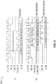
- FIG. 2 illustrates an embodiment 90 of signal timing according to the invention as shown in FIG. 1 for serializing D_TX (e.g., D_TX [7:0]), for transmission from the first chip and upon receipt at the second chip performing deserialization back into D_RX (e.g., D_RX [7:0]).
- D_TX e.g., D_TX [7:0]
- the upper portion of the figure shows signals on the transmitter (TX) while the lower section shows signals on the receiver (RX).
- a clock signal (CLK_SYS) is utilized for timing the various actions in the transmitter circuit.
- CLK_SYS is utilized to strobe DQS_RX and D_RX.
- a transmitter enable signal (TX_EN) enables data serialization and transmission.
- the TRACK_TX pulses are generated to which all D_TX data operations are synchronized during modulation.
- FIG. 2 depicts TRACK_RX and data D_RX being restored.
- a clock signal CLK_SYS
- a receiver enable signal RX_EN
- the TRACK_RX signal is shown experiencing jitter after demodulation.
- Data output from the ADCs is seen (D_after_ADC) after demodulation.
- the track pulse restore circuit will perform the restoration of data from the desired eye window and then synchronizes the data bus with the system clock.
- the DQS_RX flag signal is seen being generated as data words D_RX and are ready to be read by the receiver controller.
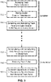
- FIG. 3 illustrates an example embodiment of the tracked method of serializing and de-serializing according to the invention.
- a track pulse start signal is used for starting track pulse generation and storing 112 a digital data word into buffers for modulation and transmission.
- the track pulses and digital data word are serialized and modulated 114 into a multi-frequency analog output for receipt, such as on another chip, by a de-serializer.
- the de-serializer the multi-frequency analog is converted 116 back to a digital data word, and the track pulse is also restored 118.
- Synchronization signals are generated in response to the restored track pulse for collecting 120 the digital data word for output. It will be noted that synchronization signals are generated in response to the track pulse for: (1) triggering the digital output to the buffers from the ADCs, (2) latching digital data onto the buffers; and (3) signaling that a digital data word is ready.
Landscapes
- Engineering & Computer Science (AREA)
- Theoretical Computer Science (AREA)
- General Engineering & Computer Science (AREA)
- Physics & Mathematics (AREA)
- General Physics & Mathematics (AREA)
- Computer Hardware Design (AREA)
- Computer Networks & Wireless Communication (AREA)
- Signal Processing (AREA)
- Digital Transmission Methods That Use Modulated Carrier Waves (AREA)
- Transceivers (AREA)
- Dc Digital Transmission (AREA)
Description
- This invention pertains generally to chip-to-chip communications, and more particularly to a self tracking serializer de-serializer.
- Conventional serializer de-serializer I/O is based on multiplexing and demultiplexing digital communications. Using such conventional schemes to increase communications bandwidth requires increasing clock rate.
- Attempting to use multi-frequency bands in a traditional scheme for modulation and demodulation to overcome the above problems brings up additional issues. Current multi-frequency serializers and de-serializers for use with chip-to-chip I/O include modulation and demodulation that are complicated and dependent on external factors, such as silicon process, connection conditions, power supply quality, and the like. In these conventional systems, a complicated scheme, such as error correction or base band processing is required to achieve reliable modulation and demodulation with low bit error rate. When the latency of modulation and demodulation becomes critical in the I/O connection, the traditional base band processing, used to ensure low bit-error-rate (BER), in modulation and demodulation becomes impractical.
- The use of base band processing techniques can in some cases provide for reliable data transmission and reception, yet it comes with a high cost penalty regarding circuit complexity and unnecessarily long delays for data processing. Although the typical multi-frequency approach may be suitable for high throughput operations, it is not well suited when short latencies are required to perform mission critical operations.
- Accordingly, a need exists for chip-to-chip multi-frequency communication circuits that have short latencies and are readily implemented. The present invention fulfills these needs, and overcomes shortcomings of previous multi-frequency chip-to-chip communication topologies.
-
US4888792 discloses a multi-level quadrature amplitude modulation and demodulation system that includes a first exchange circuit for cyclicly exchanging input digital signals and for outputting exchanged signals to D/A converters. The D/A converters provide analog signals to a QAM modulator which produces a modulated signal. In the receiver side of the system, a QAM demodulator demodulates the modulated signal to produce analog signals which are converted to digital exchanged signals by A/D converters. The digital exchanged signals are exchanged in a manner which is the reverse of that of the first exchange circuit to provide output digital signals on output terminals which respectively correspond to the input terminals. By cyclicly exchanging the input signals in this manner, the transmission quality for each of the input signal channels is maintained equal. - This invention concerns an apparatus and method for serializing and de-serializing chip-to-chip communications as defined in the independent claims 1 and 6. A chip-to-chip serializer and de-serializer are described which utilize a self tracking method based on track pulse generation on the transmitter (TX) and track pulse restoration on the receiver (RX). The data to be transmitted is synchronized with the generated track pulse on TX, with the transmitted data and track pulse being modulated at the same time in the TX. All signals communicated chip-to-chip utilizing the present invention are processed under the same conditions, including silicon process variation, power noise, critical path delay, and so forth, thus eliminating/reducing the impact of these variables on operation of the serializer de-serializer.
- Utilizing the inventive self-tracking serializer de-serializer, one can reach the performance limitation for any given technology by not only increasing the data throughput, but in response to also reducing data transfer latency.
- The signals are serialized, modulated and transmitted through a short I/O connection from transmitter (TX) to receiver (RX). The RX also demodulates all signals under the same conditions and characteristics of the receiver. The track pulse is restored in the RX after demodulation. Because the data and track pulse are synchronized in the TX, the signals should likewise be synchronized in the RX when all signals are processed with identical demodulation. Once the track pulse is restored, the self track scheme can sample the restored data at the correct timing. The sample timing tracks the external factors even under different operating conditions, use of different integrated circuit chips or different process technology. The next level of synchronization with the system bus after the signal is sampled in the analog-to-digital converter (ADC) which can also be processed based on the timing of restored track pulse.
- The restored track pulse can experience significant jitter in practice. By further use of over-sampling techniques to build a restored track pulse, the implementation provides an improved large jitter tolerance.
- The inventive self tracking serializer de-serializer provides significant improvements to the yield of chip-to-chip I/O circuits. The inventive system can be ported to fabricate devices compatible with future silicon process advancements, such as from 28 nm nodes to 14 or 20 nm nodes with minor effort.
- Further aspects of the invention will be brought out in the following portions of the specification, wherein the detailed description is for the purpose of fully disclosing preferred embodiments of the invention without placing limitations thereon.
- The invention will be more fully understood by reference to the following drawings which are for illustrative purposes only:
-
FIG. 1A andFIG. 1B is a block diagram of a self-tracking multi-frequency band serializer and de-serializer according to an embodiment of the present invention. -
FIG. 2 is a timing diagram of track pulse generation and restoration within a self-tracking multi-frequency band serializer and de-serializer according to an embodiment of the present invention. -
FIG. 3 is a flow diagram of a self tracking serializer de-serializer method according to an embodiment of the present invention. - A self tracking serializer de-serializer is described in which a track pulse is generated which travels along with the digital data through serialization and modulation at the transmitter (i.e., first chip) and the demodulation and de-serialization at the receiver (i.e., second chip). This self tracking ability allows one to build a circuit with minimum timing overhead without complicated base band processing, while performance and device yield are achieved with low circuit overhead. Integrated circuits can be fabricated using this self track mechanism in any desired device technology or process, including 28 nm or use of advanced silicon process technologies.
-
FIG. 1A andFIG. 1B illustrate anexample embodiment 10 for a self tracking multi-frequency band serializer and de-serializer, shown for communicating between a transmitter (TX) in afirst chip 12 seen inFIG. 1A over an I/O channel 14, to a receiver (RX) in asecond chip 16 seen inFIG. 1B . - Digital data 18 (DQ_TX) and byte mask 19 (DM_TX) is seen received in the TX in
FIG. 1A . The byte mask is utilized when the data word to be communicated is sent in multiple sections (e.g., 16 bits over the 8 bit path shown inFIG. 1A ,FIG. 1B ). Although the example embodiment often describes a structure allowing sending of 8 bits of digital data (e.g., [7:0]), it will be appreciated that the present invention can be configured with any desired number of bits (e.g., 16 bits, 32 bits, and so forth). However, this requires adding more data buffers, converters (DAC, ADC), and modulators and demodulators operating at more frequencies or with higher order encoding. - The transmitter controller asserts a synchronization signal 20 (DQS_TX) flag to trigger tracking and serialization. In any embodiment of the invention, the DQS_TX pulse traverses the whole propagation path to which the data is subject. A
track pulse generator 24 receives synchronization signal 20 (DQS_TX) and aclock signal 22. The track pulse generator is configured to generate a synchronized pulse as the flag for data synchronization. It is shown in the figure that DQS_TX is also applied to a buffer for data mask (DM_TX) 19 and as a first input of the data buffers 26a, 26b, 26c, on through to 26m and 26n, which also receive bits withindata DQ_TX 18 so that data synchronizes with the track pulse. - The track pulse and digital data word are serialized and modulated for transmission to the receiver. Bits of
data DQ_TX 18 along with a track pulse fromtrack pulse generator 24 atmodulators controllers FIG. 1A andFIG. 1B , respectively. In one example, each modulator utilizes quadrature amplitude modulation (QAM) (e.g., QAM16) and has mixers which encode both an I channel and a Q channel of information into a given modulation frequency. - It will be appreciated that QAM, as described in this embodiment, is an analog modulation mechanism, which differs from digital multiplexing used in a digital serialization scheme. In analog QAM, two analog message signals are communicated on each frequency channel by changing (modulating) two carrier waves. The two carrier waves (typically sinusoids), are out of phase with each other by 90° and are thus called quadrature carriers. Output over a frequency channel is the sum of the modulated waves of phase modulation (PM) and amplitude modulation (AM). For the sake of simplicity of description, the internal circuitry for analog QAM is not described. It will be noted that a large number of QAM circuits are available and the technology is well known to one of ordinary skill in the art. It should be appreciated that a variety of forms of QAM are available and can be utilized with the present invention, some of the more common forms that can be selected for use include: QAM8, QAM16, QAM32, QAM64, QAM128, and QAM256. It will be appreciated that QAM distributes information in the I-Q plane evenly, and the higher orders of QAM involve information spaced more closely in the constellation. Thus, higher order QAM allows transmitting more bits per symbol, but if the energy of the constellation is to remain the same, the points on the constellation are closer together and the transmission becomes more susceptible to noise. It should also be appreciated that other forms of modulation (demodulation) can be utilized in the present invention without departing from the teachings herein. Examples of other forms of multi-frequency modulation which can be utilized include pulse-width modulation (PWM), frequency-shift keying (FSK), frequency-hopping, spread spectrum, and so forth.
- During serialization and modulation in
FIG. 1A , digital data is converted by digital-to-analog converter (DAC) 30a, 30b, resulting in analog outputs received atmixers modulators O channel 14 and thus travel through the same I/O connection for receipt atsecond chip 16. This configuration assures a close tracking of the data path through the same modulation process as the tracking signal, regardless of the various channel conditions of I/O channel 14. - In the receiver (RX) 16 seen in
FIG. 1B , all signals are demodulated through the same path, exemplified withdemodulators - One of the ADCs is seen outputting digital data to a track pulse restore
circuit 40, which operates in combination withoutput data buffers first output 44, comprises the restored track pulse itself used to synchronize the output from the ADCs to the data buffers. Track pulse restorecircuit 40 receives a clock 46 (CLK_SYS), and outputs a synchronization signal (pulse) 48 for controlling the latching of data from the ADCs at each of the data buffers whose output is de-serialized digital data (DQ_RX) 52. Once data from the ADCs is latched to the data buffer, the track pulse restoration circuit sets aflag DQS_RX 50, signaling that the receiver controller can now read the DQ_RX data word. A byte mask (DM_RX) 51 is also generated for masking purposes when handling multiple bytes. - It will be seen that the track pulse and all data follow through the same path and time, thus allowing the track pulse restoration circuit to generate signals for controlling ADC output and latching of the data into the buffers with proper timing.
- The above serializer and de-serializer are particularly well-suited for operation on a first chip and a second chip between which communication is to be established. It will be appreciated that a second I/O channel can be utilized for establishing a communication path in the opposite direction between the first and second chips. This first and second chips seen in
FIG. 1A andFIG. 1B are each configured with acontroller processor circuit 64, comprisingCPU 68 withmemory 70, and utilizing aclock circuit 66. In a similarmanner RX controller 74 is shown having at least oneprocessor circuit 76, comprisingCPU 78 withmemory 80, and utilizing aclock circuit 82. It will be appreciated, however, that controller circuits can be implemented with various combinations of discrete and programmable logic circuits and processors, without departing from the teachings of the present invention. -
FIG. 2 illustrates anembodiment 90 of signal timing according to the invention as shown inFIG. 1 for serializing D_TX (e.g., D_TX [7:0]), for transmission from the first chip and upon receipt at the second chip performing deserialization back into D_RX (e.g., D_RX [7:0]). The upper portion of the figure shows signals on the transmitter (TX) while the lower section shows signals on the receiver (RX). A clock signal (CLK_SYS) is utilized for timing the various actions in the transmitter circuit. The rising edge of CLK_SYS is utilized to strobe DQS_RX and D_RX. A transmitter enable signal (TX_EN) enables data serialization and transmission. Upon asserting DQS_TX, the TRACK_TX pulses are generated to which all D_TX data operations are synchronized during modulation. - The lower portion of
FIG. 2 depicts TRACK_RX and data D_RX being restored. A clock signal (CLK_SYS) is utilized for timing the various actions in the receiver circuit. A receiver enable signal (RX_EN) enables data deserialization. The TRACK_RX signal is shown experiencing jitter after demodulation. Data output from the ADCs is seen (D_after_ADC) after demodulation. The track pulse restore circuit will perform the restoration of data from the desired eye window and then synchronizes the data bus with the system clock. The DQS_RX flag signal is seen being generated as data words D_RX and are ready to be read by the receiver controller. -
FIG. 3 illustrates an example embodiment of the tracked method of serializing and de-serializing according to the invention. Beginning withstep 110, a track pulse start signal is used for starting track pulse generation and storing 112 a digital data word into buffers for modulation and transmission. The track pulses and digital data word are serialized and modulated 114 into a multi-frequency analog output for receipt, such as on another chip, by a de-serializer. In the de-serializer, the multi-frequency analog is converted 116 back to a digital data word, and the track pulse is also restored 118. Synchronization signals are generated in response to the restored track pulse for collecting 120 the digital data word for output. It will be noted that synchronization signals are generated in response to the track pulse for: (1) triggering the digital output to the buffers from the ADCs, (2) latching digital data onto the buffers; and (3) signaling that a digital data word is ready. - From the discussion above it will be appreciated that the invention can be embodied in various ways, including the following:
- 1. An apparatus for serializing and de-serializing chip-to-chip communications, comprising: a serializer configured for serializing and modulating digital data bits, said serializer having a track pulse generator and data buffers whose digital data bit outputs are modulated by multiple modulators into multiple analog frequency signals configured for communication over an I/O channel to an off chip de-serializer; and a de-serializer having multiple demodulators configured for receiving said multiple analog frequency signals over the I/O channel and demodulating these signals for receipt by a track pulse restoration circuit and data buffers; wherein said track pulse restoration circuit generates synchronization signals for triggering output from said demodulators to said receiver data buffers, latching data into said receiver data buffers, and signaling that digital data bits can be read from said receiver data buffers.
- 2. The apparatus of any of the previous embodiments, wherein said modulator and said demodulator operate utilizing quadrature amplitude modulation (QAM).
- 3. The apparatus of any of the previous embodiments, wherein said modulator and said demodulator operate utilizing quadrature amplitude modulation (QAM), selected from the group of QAM orders consisting of QAM8, QAM16, QAM32, QAM64, QAM128 or QAM256.
- 4. The apparatus of any of the previous embodiments, wherein said quadrature amplitude modulation (QAM) encodes two analog message signals into carrier waves at its carrier frequency.
- 5. The apparatus of any of the previous embodiments, wherein said digital data bits comprises at least 8 bits.
- 6. An apparatus for serializing and de-serializing chip-to-chip communications, comprising: a track pulse generator, configured for generating track pulses, within a serializer configured for serializing words of digital data into multiple analog frequency signals for communication to an off chip de-serializer; multiple transmitter data buffers configured for receiving digital data bits; wherein said multiple transmitter data buffers load data bits in response to receipt of a synchronization signal which is also received at said track pulse generator; multiple modulator circuits, each modulator circuit operating at a different modulation frequency; said modulator circuits are configured for converting said track pulses and outputs from said multiple transmitter data buffers into an analog signal modulated into carriers signals at multiple frequencies for transmission to a de-serializer; and multiple demodulator circuits within a de-serializer configured for demodulating and de-serializing data from multiple analog frequency signals received from a serializer, and outputting digital data; wherein each demodulator circuit operates at a different modulation frequency; wherein said demodulator circuits are configured for converting analog signals modulated into carriers signals at multiple frequencies into words of digital data; a track pulse restoration circuit, configured for restoring the track pulse from the transmitter and generating multiple synchronization signals; multiple receiver data buffers configured for receiving digital data bits from said demodulator circuits; wherein output of digital data from each said demodulator is triggered in response to a first synchronization signal from said track pulse restoration circuit; wherein said digital data from each said demodulator is latched into each of said multiple receiver data buffers in response to receipt of a second synchronization signal from said track pulse restoration circuit; and wherein said digital data is read from said data buffers in response to a third synchronization signal from said track pulse restoration circuit.
- 7. The apparatus of any of the previous embodiments, wherein said modulation and demodulation utilizes quadrature amplitude modulation (QAM).
- 8. The apparatus of any of the previous embodiments, wherein said QAM is selected from the group of QAM orders consisting of QAM8, QAM16, QAM32, QAM64, QAM128 or QAM256.
- 9. The apparatus of any of the previous embodiments, wherein said quadrature amplitude modulation (QAM) encodes two analog message signals into carrier waves at each output frequency.
- 10. The apparatus of any of the previous embodiments, wherein said digital data bits comprises at least 8 bits.
- 11. A method for serializing and de-serializing chip-to-chip communications, comprising: generating track pulses within a serializer of a first device chip; storing a digital data word for transmission from the first device chip; serializing said track pulses and said digital data word and modulating them into multiple frequency analog signals for communication a de-serializer in a second chip; demodulating the multiple frequency analog signals received at a second device chip; performing restoration of the track pulse received from said first device chip; and controlling the collection of said digital data word into output buffers in response to synchronization signals timed in relation to restoration of the track pulse.
- 12. The method of any of the previous embodiments, wherein said storing a digital data word for transmission is performed with multiple transmitter data buffers which load data bits in response to receipt of a synchronization signal which is also received at a track pulse generator which generates said track pulses.
- 13. The method of any of the previous embodiments, wherein said serializing and modulating into multiple frequency analog signals is performed by multiple modulator circuits, each modulator circuit operating at a different modulation frequency.
- 14. The method of any of the previous embodiments, wherein each said modulator circuit contains digital-to-analog converters (DACs) coupled to modulating mixers.
- 15. The method of any of the previous embodiments, wherein said modulating and demodulating is performed in response to a quadrature amplitude modulation (QAM) technique.
- 16. The method of any of the previous embodiments, wherein said quadrature amplitude modulation (QAM) encodes two analog message signals into carrier waves at each output frequency.
- 17. The method of any of the previous embodiments, wherein said quadrature amplitude modulation (QAM) is selected from the group of QAM orders consisting of QAM8, QAM16, QAM32, QAM64, QAM128 or QAM256.
- 18. The method of any of the previous embodiments, wherein said de-serializing and demodulating from multiple frequency analog signals is performed by multiple demodulator circuits, each demodulator circuit operating at a different modulation frequency.
- 19. The method of any of the previous embodiments, wherein each said demodulator circuit contains analog-to-digital converters (ADCs) coupled to demodulating mixers.
- 20. The method of any of the previous embodiments, wherein said synchronization signals timed in relation to restoration of the track pulse, comprises: a first synchronization signal which triggers demodulator output of digital data to data buffers; a second synchronization signal which latches said digital data onto the data buffers; and a third synchronization signal which indicates that the latched digital data can be read from the buffers.
- Although the description above contains many details, these should not be construed as limiting the scope of the invention but as merely providing illustrations of some of the presently preferred embodiments of this invention. Therefore, it will be appreciated that the scope of the present invention fully encompasses other embodiments which may become obvious to those skilled in the art, and that the scope of the present invention is accordingly to be limited by nothing other than the appended claims, in which reference to an element in the singular is not intended to mean "one and only one" unless explicitly so stated, but rather "one or more." All structural and functional equivalents to the elements of the above-described preferred embodiment that are known to those of ordinary skill in the art are expressly incorporated herein by reference and are intended to be encompassed by the present claims. Moreover, it is not necessary for a device or method to address each and every problem sought to be solved by the present invention, for it to be encompassed by the present claims. Furthermore, no element, component, or method step in the present disclosure is intended to be dedicated to the public regardless of whether the element, component, or method step is explicitly recited in the claims. No claim element herein is to be construed under the provisions of 35 U.S.C. 112, sixth paragraph, unless the element is expressly recited using the phrase "means for."
Claims (15)
- An apparatus (10) for serializing (12) and de-serializing (16) chip-to-chip communications, comprising:a serializer (12) configured for serializing and modulating digital data bits, said serializer having a track pulse generator (24) and data buffers (26a-26n) whose digital data bit outputs are modulated by multiple modulators (28a - 28n) into multiple analog frequency signals configured for communication over an I/O channel (14) to an off chip de-serializer (16);wherein said track pulse generator receives a synchronization signal (20) and a clock signal (22) and said track pulse generator is configured to generate a synchronized pulse as a flag for data synchronization for each bit communicated, so that said synchronized pulse is modulated along with the digital data bit outputs by said multiple modulators (28a - 28n); anda de-serializer (16) having multiple demodulators (34a - 34 n) configured for receiving said multiple analog frequency signals over the I/O channel (14) and demodulating these signals for receipt by a track pulse restoration circuit (40) and data buffers (42a - 42n);wherein said track pulse restoration circuit (40) generates synchronization signals (48) for triggering output from said demodulators to said receiver data buffers (42a - 42n), latching data into said receiver data buffers (42a - 42n), and signaling that digital data bits can be read from said receiver data buffers.
- The apparatus recited in claim 1, wherein said modulator (28a - 28n) and said demodulator (34a - 34n) operate utilizing quadrature amplitude modulation known as QAM-.
- The apparatus recited in claim 1, wherein said modulator (28a - 28n) and said demodulator (34a - 34n) operate utilizing quadrature amplitude modulation, known as QAM, selected from the group of QAM orders consisting of QAM8, QAM16, QAM32, QAM64, QAM128 or QAM256.
- The apparatus recited in claim 1, wherein said quadrature amplitude modulation, known as QAM, encodes two analog message signals (32a, 32b) into carrier waves at its carrier frequency.
- The apparatus recited in claim 1, wherein said digital data bits (18) comprise at least 8 bits.
- A method for serializing and de-serializing chip-to-chip communications, comprising:generating track pulses (110) within a serializer of a first device chip;storing a digital data word (112) for transmission from the first device chip;serializing said track pulses (114) and said digital data word and modulating (114) them into multiple frequency analog signals for communication to a de-serializer in a second chip;wherein said track pulses are generated in response to receiving a synchronization signal (20) and a clock signal (22), and said track pulses comprise a synchronized pulse utilized as a flag for data synchronization of each bit communicated, so that said synchronized pulse is modulated along with the digital data word outputs by said multiple modulators (28a - 28n);demodulating the multiple frequency analog signals (116) received at a second device chip;performing restoration of the track pulse (118) received from said first device chip; andcontrolling the collection of said digital data word (120) into output buffers in response to synchronization signals timed in relation to restoration of the track pulse.
- The method recited in claim 6, wherein said storing a digital data word for transmission is performed with multiple transmitter data buffers (26a - 26n) which load data bits (18) in response to receipt of a synchronization signal (20) which is also received at a track pulse generator which generates said track pulses.
- The method recited in claim 6, wherein said serializing and modulating into multiple frequency analog signals is performed by multiple modulator circuits (28a - 28n), each modulator circuit operating at a different modulation frequency.
- The method recited in claim 8, wherein each said modulator circuit (28a - 28n) contains digital-to-analog converters, known as DACs, (30a, 30b) coupled to modulating mixers (32a, 32b).
- The method recited in claim 6, wherein said modulating (28a - 28n) and demodulating (34a - 34n) is performed in response to a quadrature amplitude modulation, known as QAM, technique.
- The method recited in claim 10, wherein said quadrature amplitude modulation, known as QAM, encodes two analog message signals (32a, 32b) into carrier waves at each output frequency.
- The method recited in claim 10, wherein said quadrature amplitude modulation, known as QAM, (28a - 28n) is selected from the group of QAM orders consisting of QAM8, QAM16, QAM32, QAM64, QAM128 or QAM256.
- The method recited in claim 6, wherein said de-serializing and demodulating from multiple frequency analog signals is performed by multiple demodulator circuits (34a - 34n), each demodulator circuit operating at a different modulation frequency.
- The method recited in claim 13, wherein each said demodulator circuit (34a - 34n) contains analog-to-digital converters, known as ADCs, (38a - 38n) coupled to demodulating mixers (36a - 36n).
- The method recited in claim 6, wherein said synchronization signals timed in relation to restoration of the track pulse, comprises:a first synchronization signal (44) which triggers demodulator output of digital data to data buffers;a second synchronization signal (48) which latches said digital data onto the data buffers; anda third synchronization signal (50) which indicates that the latched digital data can be read from the buffers.
Applications Claiming Priority (2)
| Application Number | Priority Date | Filing Date | Title |
|---|---|---|---|
| US201261723284P | 2012-11-06 | 2012-11-06 | |
| PCT/US2013/066194 WO2014074301A1 (en) | 2012-11-06 | 2013-10-22 | Self track scheme for multi frequency band serializer de-serializer i/o circuits |
Publications (3)
| Publication Number | Publication Date |
|---|---|
| EP2917841A1 EP2917841A1 (en) | 2015-09-16 |
| EP2917841A4 EP2917841A4 (en) | 2016-07-13 |
| EP2917841B1 true EP2917841B1 (en) | 2019-04-10 |
Family
ID=50685070
Family Applications (1)
| Application Number | Title | Priority Date | Filing Date |
|---|---|---|---|
| EP13854083.6A Active EP2917841B1 (en) | 2012-11-06 | 2013-10-22 | Self track scheme for multi frequency band serializer de-serializer i/o circuits |
Country Status (5)
| Country | Link |
|---|---|
| US (1) | US9426016B2 (en) |
| EP (1) | EP2917841B1 (en) |
| CN (1) | CN104854569B (en) |
| TW (1) | TWI584129B (en) |
| WO (1) | WO2014074301A1 (en) |
Families Citing this family (4)
| Publication number | Priority date | Publication date | Assignee | Title |
|---|---|---|---|---|
| US10614027B2 (en) * | 2015-05-18 | 2020-04-07 | Tsvlink Corp. | Serial bus with embedded side band communication |
| US11509400B2 (en) * | 2019-11-15 | 2022-11-22 | AuthenX Inc. | Image transmission system and image transmission method |
| US12579085B1 (en) | 2024-11-26 | 2026-03-17 | Texas Milkyway Inc. | Multi-bus replicator using RF serializer/deserializer for chip-to-chip interconnect |
| US12574022B1 (en) | 2025-03-14 | 2026-03-10 | Texas Milkyway Inc. | Serdes transmitter and receiver utilizing single frequency phase amplitude modulation |
Family Cites Families (15)
| Publication number | Priority date | Publication date | Assignee | Title |
|---|---|---|---|---|
| FR2192752A5 (en) * | 1972-07-10 | 1974-02-08 | Ibm France | |
| JPS6455942A (en) | 1987-08-27 | 1989-03-02 | Fujitsu Ltd | Multi-value quadrature amplitude modulation demodulation system |
| EP1371200B1 (en) * | 2001-03-01 | 2011-10-12 | Broadcom Corporation | Compensation of distortion due to channel and to receiver, in a parallel transmission system |
| US7561855B2 (en) * | 2002-06-25 | 2009-07-14 | Finisar Corporation | Transceiver module and integrated circuit with clock and data recovery clock diplexing |
| ATE362683T1 (en) * | 2004-01-06 | 2007-06-15 | Ibm | MODULATION AND DEMODULATION OF OFDM SIGNALS |
| US8731007B2 (en) * | 2005-12-30 | 2014-05-20 | Remec Broadband Wireless, Llc | Digital microwave radio link with a variety of ports |
| US7688237B2 (en) * | 2006-12-21 | 2010-03-30 | Broadcom Corporation | Apparatus and method for analog-to-digital converter calibration |
| ES2326152B1 (en) * | 2006-12-29 | 2010-06-29 | Universitat Politecnica De Catalunya (Upc) | HOMODINE RECEIVER FOR OPTICAL COMMUNICATIONS WITH PROCESSING AFTER. |
| US8582705B2 (en) * | 2007-12-10 | 2013-11-12 | Ciena Corporation | Serializer-deserializer circuit with multi-format and multi-data rate capability |
| US20110033007A1 (en) * | 2007-12-19 | 2011-02-10 | Zerbe Jared L | Multi-band, multi-drop chip to chip signaling |
| KR100961819B1 (en) * | 2008-01-04 | 2010-06-08 | 한국과학기술원 | All-optical Discrete / Inverse Discrete Fourier Converter for Optical OPM Communication, Method thereof, and Transceiver including the Same |
| US8107814B2 (en) * | 2008-07-25 | 2012-01-31 | Cisco Technology, Inc. | Transporting upstream data in a passive optical network |
| CN102201810A (en) * | 2010-03-23 | 2011-09-28 | 奇景光电股份有限公司 | Apparatus for controlling clock recovery and method thereof |
| CN201904844U (en) * | 2010-12-08 | 2011-07-20 | 南开大学 | Digital audio-video signal SerDes |
| US9374166B2 (en) * | 2012-02-13 | 2016-06-21 | Ciena Corporation | High speed optical communication systems and methods with flexible bandwidth adaptation |
-
2013
- 2013-10-22 CN CN201380057582.0A patent/CN104854569B/en active Active
- 2013-10-22 EP EP13854083.6A patent/EP2917841B1/en active Active
- 2013-10-22 WO PCT/US2013/066194 patent/WO2014074301A1/en not_active Ceased
- 2013-10-31 TW TW102139524A patent/TWI584129B/en active
-
2015
- 2015-05-05 US US14/704,694 patent/US9426016B2/en active Active
Non-Patent Citations (1)
| Title |
|---|
| None * |
Also Published As
| Publication number | Publication date |
|---|---|
| CN104854569B (en) | 2018-01-05 |
| TW201443655A (en) | 2014-11-16 |
| EP2917841A4 (en) | 2016-07-13 |
| CN104854569A (en) | 2015-08-19 |
| TWI584129B (en) | 2017-05-21 |
| US9426016B2 (en) | 2016-08-23 |
| US20150312083A1 (en) | 2015-10-29 |
| EP2917841A1 (en) | 2015-09-16 |
| WO2014074301A1 (en) | 2014-05-15 |
Similar Documents
| Publication | Publication Date | Title |
|---|---|---|
| US10785015B1 (en) | Multiple phase symbol synchronization for amplifier sampler accepting modulated signal | |
| CN112241384B (en) | Universal high-speed serial differential signal shunt circuit and method | |
| Fettweis et al. | Zero crossing modulation for communication with temporally oversampled 1-bit quantization | |
| US20040212416A1 (en) | Phase interpolator device and method | |
| Kim et al. | An 800 Mbps multi-channel CMOS serial link with 3/spl times/oversampling | |
| EP2917841B1 (en) | Self track scheme for multi frequency band serializer de-serializer i/o circuits | |
| CN107409038B (en) | Full Duplex Radio in Wireless Tunneling System | |
| CN104125052A (en) | Parallel timing synchronization system and method | |
| KR102252121B1 (en) | Differential current mode low latency modulation and demodulation for chip-to-chip connection | |
| US8144761B2 (en) | Pulse transmission method, pulse transmission system, transmitter, and receiver | |
| CN112840571A (en) | A cross-clock domain processing circuit | |
| CN116582236A (en) | Burst frame, burst frame transmission method and device, device and storage medium | |
| US8861648B2 (en) | Receiving device and demodulation device | |
| US11088880B2 (en) | Phase modulated data link for low-swing wireline applications | |
| US7283011B2 (en) | Method for performing dual phase pulse modulation | |
| US20140140380A1 (en) | Initialization sequence for bi-directional communications in a carrier-based system | |
| US9491028B2 (en) | Phase synchronization of modulation or demodulation for QAM-based multiband TSV-link | |
| US6922160B1 (en) | Scalable bus system and method for communicating digital data using analog modulation and demodulation | |
| WO2022193328A1 (en) | Serializing/deserializing circuit, serial data receiving method, and chip | |
| Seo et al. | A 12-Gb/s baud-rate clock and data recovery with 75% phase-detection probability by precoding and integration-hold-reset frontend | |
| Yuce et al. | The performance and experimental results of a multiple bit rate symbol timing recovery circuit for PSK receivers | |
| JP3531829B2 (en) | Orthogonal frequency division multiplexing signal transmission / reception system and orthogonal frequency division multiplexing signal transmission / reception method | |
| Talal | Modem design for digital satellite communications | |
| JP2002237799A (en) | Quadrature frequency division multiplex signal receiver | |
| JP2002237798A (en) | Quadrature frequency division multiplex signal receiver |
Legal Events
| Date | Code | Title | Description |
|---|---|---|---|
| PUAI | Public reference made under article 153(3) epc to a published international application that has entered the european phase |
Free format text: ORIGINAL CODE: 0009012 |
|
| 17P | Request for examination filed |
Effective date: 20150529 |
|
| AK | Designated contracting states |
Kind code of ref document: A1 Designated state(s): AL AT BE BG CH CY CZ DE DK EE ES FI FR GB GR HR HU IE IS IT LI LT LU LV MC MK MT NL NO PL PT RO RS SE SI SK SM TR |
|
| AX | Request for extension of the european patent |
Extension state: BA ME |
|
| DAX | Request for extension of the european patent (deleted) | ||
| RA4 | Supplementary search report drawn up and despatched (corrected) |
Effective date: 20160615 |
|
| RIC1 | Information provided on ipc code assigned before grant |
Ipc: G06F 13/38 20060101ALI20160609BHEP Ipc: G06F 13/42 20060101ALI20160609BHEP Ipc: G06F 13/00 20060101AFI20160609BHEP |
|
| RIC1 | Information provided on ipc code assigned before grant |
Ipc: G06F 13/00 20060101AFI20180907BHEP Ipc: G06F 13/38 20060101ALI20180907BHEP Ipc: G06F 13/42 20060101ALI20180907BHEP |
|
| GRAP | Despatch of communication of intention to grant a patent |
Free format text: ORIGINAL CODE: EPIDOSNIGR1 |
|
| STAA | Information on the status of an ep patent application or granted ep patent |
Free format text: STATUS: GRANT OF PATENT IS INTENDED |
|
| INTG | Intention to grant announced |
Effective date: 20181031 |
|
| GRAS | Grant fee paid |
Free format text: ORIGINAL CODE: EPIDOSNIGR3 |
|
| GRAA | (expected) grant |
Free format text: ORIGINAL CODE: 0009210 |
|
| STAA | Information on the status of an ep patent application or granted ep patent |
Free format text: STATUS: THE PATENT HAS BEEN GRANTED |
|
| AK | Designated contracting states |
Kind code of ref document: B1 Designated state(s): AL AT BE BG CH CY CZ DE DK EE ES FI FR GB GR HR HU IE IS IT LI LT LU LV MC MK MT NL NO PL PT RO RS SE SI SK SM TR |
|
| REG | Reference to a national code |
Ref country code: GB Ref legal event code: FG4D |
|
| REG | Reference to a national code |
Ref country code: CH Ref legal event code: EP Ref country code: AT Ref legal event code: REF Ref document number: 1119632 Country of ref document: AT Kind code of ref document: T Effective date: 20190415 |
|
| REG | Reference to a national code |
Ref country code: IE Ref legal event code: FG4D |
|
| REG | Reference to a national code |
Ref country code: DE Ref legal event code: R096 Ref document number: 602013053848 Country of ref document: DE |
|
| REG | Reference to a national code |
Ref country code: NL Ref legal event code: MP Effective date: 20190410 |
|
| REG | Reference to a national code |
Ref country code: LT Ref legal event code: MG4D |
|
| REG | Reference to a national code |
Ref country code: AT Ref legal event code: MK05 Ref document number: 1119632 Country of ref document: AT Kind code of ref document: T Effective date: 20190410 |
|
| PG25 | Lapsed in a contracting state [announced via postgrant information from national office to epo] |
Ref country code: NL Free format text: LAPSE BECAUSE OF FAILURE TO SUBMIT A TRANSLATION OF THE DESCRIPTION OR TO PAY THE FEE WITHIN THE PRESCRIBED TIME-LIMIT Effective date: 20190410 |
|
| PG25 | Lapsed in a contracting state [announced via postgrant information from national office to epo] |
Ref country code: NO Free format text: LAPSE BECAUSE OF FAILURE TO SUBMIT A TRANSLATION OF THE DESCRIPTION OR TO PAY THE FEE WITHIN THE PRESCRIBED TIME-LIMIT Effective date: 20190710 Ref country code: FI Free format text: LAPSE BECAUSE OF FAILURE TO SUBMIT A TRANSLATION OF THE DESCRIPTION OR TO PAY THE FEE WITHIN THE PRESCRIBED TIME-LIMIT Effective date: 20190410 Ref country code: PT Free format text: LAPSE BECAUSE OF FAILURE TO SUBMIT A TRANSLATION OF THE DESCRIPTION OR TO PAY THE FEE WITHIN THE PRESCRIBED TIME-LIMIT Effective date: 20190910 Ref country code: AL Free format text: LAPSE BECAUSE OF FAILURE TO SUBMIT A TRANSLATION OF THE DESCRIPTION OR TO PAY THE FEE WITHIN THE PRESCRIBED TIME-LIMIT Effective date: 20190410 Ref country code: ES Free format text: LAPSE BECAUSE OF FAILURE TO SUBMIT A TRANSLATION OF THE DESCRIPTION OR TO PAY THE FEE WITHIN THE PRESCRIBED TIME-LIMIT Effective date: 20190410 Ref country code: SE Free format text: LAPSE BECAUSE OF FAILURE TO SUBMIT A TRANSLATION OF THE DESCRIPTION OR TO PAY THE FEE WITHIN THE PRESCRIBED TIME-LIMIT Effective date: 20190410 Ref country code: HR Free format text: LAPSE BECAUSE OF FAILURE TO SUBMIT A TRANSLATION OF THE DESCRIPTION OR TO PAY THE FEE WITHIN THE PRESCRIBED TIME-LIMIT Effective date: 20190410 Ref country code: LT Free format text: LAPSE BECAUSE OF FAILURE TO SUBMIT A TRANSLATION OF THE DESCRIPTION OR TO PAY THE FEE WITHIN THE PRESCRIBED TIME-LIMIT Effective date: 20190410 |
|
| PG25 | Lapsed in a contracting state [announced via postgrant information from national office to epo] |
Ref country code: RS Free format text: LAPSE BECAUSE OF FAILURE TO SUBMIT A TRANSLATION OF THE DESCRIPTION OR TO PAY THE FEE WITHIN THE PRESCRIBED TIME-LIMIT Effective date: 20190410 Ref country code: PL Free format text: LAPSE BECAUSE OF FAILURE TO SUBMIT A TRANSLATION OF THE DESCRIPTION OR TO PAY THE FEE WITHIN THE PRESCRIBED TIME-LIMIT Effective date: 20190410 Ref country code: BG Free format text: LAPSE BECAUSE OF FAILURE TO SUBMIT A TRANSLATION OF THE DESCRIPTION OR TO PAY THE FEE WITHIN THE PRESCRIBED TIME-LIMIT Effective date: 20190710 Ref country code: GR Free format text: LAPSE BECAUSE OF FAILURE TO SUBMIT A TRANSLATION OF THE DESCRIPTION OR TO PAY THE FEE WITHIN THE PRESCRIBED TIME-LIMIT Effective date: 20190711 Ref country code: LV Free format text: LAPSE BECAUSE OF FAILURE TO SUBMIT A TRANSLATION OF THE DESCRIPTION OR TO PAY THE FEE WITHIN THE PRESCRIBED TIME-LIMIT Effective date: 20190410 |
|
| PG25 | Lapsed in a contracting state [announced via postgrant information from national office to epo] |
Ref country code: AT Free format text: LAPSE BECAUSE OF FAILURE TO SUBMIT A TRANSLATION OF THE DESCRIPTION OR TO PAY THE FEE WITHIN THE PRESCRIBED TIME-LIMIT Effective date: 20190410 Ref country code: IS Free format text: LAPSE BECAUSE OF FAILURE TO SUBMIT A TRANSLATION OF THE DESCRIPTION OR TO PAY THE FEE WITHIN THE PRESCRIBED TIME-LIMIT Effective date: 20190810 |
|
| REG | Reference to a national code |
Ref country code: DE Ref legal event code: R097 Ref document number: 602013053848 Country of ref document: DE |
|
| PG25 | Lapsed in a contracting state [announced via postgrant information from national office to epo] |
Ref country code: SK Free format text: LAPSE BECAUSE OF FAILURE TO SUBMIT A TRANSLATION OF THE DESCRIPTION OR TO PAY THE FEE WITHIN THE PRESCRIBED TIME-LIMIT Effective date: 20190410 Ref country code: RO Free format text: LAPSE BECAUSE OF FAILURE TO SUBMIT A TRANSLATION OF THE DESCRIPTION OR TO PAY THE FEE WITHIN THE PRESCRIBED TIME-LIMIT Effective date: 20190410 Ref country code: EE Free format text: LAPSE BECAUSE OF FAILURE TO SUBMIT A TRANSLATION OF THE DESCRIPTION OR TO PAY THE FEE WITHIN THE PRESCRIBED TIME-LIMIT Effective date: 20190410 Ref country code: CZ Free format text: LAPSE BECAUSE OF FAILURE TO SUBMIT A TRANSLATION OF THE DESCRIPTION OR TO PAY THE FEE WITHIN THE PRESCRIBED TIME-LIMIT Effective date: 20190410 Ref country code: DK Free format text: LAPSE BECAUSE OF FAILURE TO SUBMIT A TRANSLATION OF THE DESCRIPTION OR TO PAY THE FEE WITHIN THE PRESCRIBED TIME-LIMIT Effective date: 20190410 |
|
| PLBE | No opposition filed within time limit |
Free format text: ORIGINAL CODE: 0009261 |
|
| STAA | Information on the status of an ep patent application or granted ep patent |
Free format text: STATUS: NO OPPOSITION FILED WITHIN TIME LIMIT |
|
| PG25 | Lapsed in a contracting state [announced via postgrant information from national office to epo] |
Ref country code: IT Free format text: LAPSE BECAUSE OF FAILURE TO SUBMIT A TRANSLATION OF THE DESCRIPTION OR TO PAY THE FEE WITHIN THE PRESCRIBED TIME-LIMIT Effective date: 20190410 Ref country code: SM Free format text: LAPSE BECAUSE OF FAILURE TO SUBMIT A TRANSLATION OF THE DESCRIPTION OR TO PAY THE FEE WITHIN THE PRESCRIBED TIME-LIMIT Effective date: 20190410 |
|
| 26N | No opposition filed |
Effective date: 20200113 |
|
| PG25 | Lapsed in a contracting state [announced via postgrant information from national office to epo] |
Ref country code: TR Free format text: LAPSE BECAUSE OF FAILURE TO SUBMIT A TRANSLATION OF THE DESCRIPTION OR TO PAY THE FEE WITHIN THE PRESCRIBED TIME-LIMIT Effective date: 20190410 |
|
| PG25 | Lapsed in a contracting state [announced via postgrant information from national office to epo] |
Ref country code: SI Free format text: LAPSE BECAUSE OF FAILURE TO SUBMIT A TRANSLATION OF THE DESCRIPTION OR TO PAY THE FEE WITHIN THE PRESCRIBED TIME-LIMIT Effective date: 20190410 Ref country code: MC Free format text: LAPSE BECAUSE OF FAILURE TO SUBMIT A TRANSLATION OF THE DESCRIPTION OR TO PAY THE FEE WITHIN THE PRESCRIBED TIME-LIMIT Effective date: 20190410 |
|
| REG | Reference to a national code |
Ref country code: CH Ref legal event code: PL |
|
| PG25 | Lapsed in a contracting state [announced via postgrant information from national office to epo] |
Ref country code: LU Free format text: LAPSE BECAUSE OF NON-PAYMENT OF DUE FEES Effective date: 20191022 Ref country code: LI Free format text: LAPSE BECAUSE OF NON-PAYMENT OF DUE FEES Effective date: 20191031 Ref country code: CH Free format text: LAPSE BECAUSE OF NON-PAYMENT OF DUE FEES Effective date: 20191031 |
|
| REG | Reference to a national code |
Ref country code: BE Ref legal event code: MM Effective date: 20191031 |
|
| PG25 | Lapsed in a contracting state [announced via postgrant information from national office to epo] |
Ref country code: BE Free format text: LAPSE BECAUSE OF NON-PAYMENT OF DUE FEES Effective date: 20191031 |
|
| PG25 | Lapsed in a contracting state [announced via postgrant information from national office to epo] |
Ref country code: IE Free format text: LAPSE BECAUSE OF NON-PAYMENT OF DUE FEES Effective date: 20191022 |
|
| PG25 | Lapsed in a contracting state [announced via postgrant information from national office to epo] |
Ref country code: CY Free format text: LAPSE BECAUSE OF FAILURE TO SUBMIT A TRANSLATION OF THE DESCRIPTION OR TO PAY THE FEE WITHIN THE PRESCRIBED TIME-LIMIT Effective date: 20190410 |
|
| PG25 | Lapsed in a contracting state [announced via postgrant information from national office to epo] |
Ref country code: HU Free format text: LAPSE BECAUSE OF FAILURE TO SUBMIT A TRANSLATION OF THE DESCRIPTION OR TO PAY THE FEE WITHIN THE PRESCRIBED TIME-LIMIT; INVALID AB INITIO Effective date: 20131022 Ref country code: MT Free format text: LAPSE BECAUSE OF FAILURE TO SUBMIT A TRANSLATION OF THE DESCRIPTION OR TO PAY THE FEE WITHIN THE PRESCRIBED TIME-LIMIT Effective date: 20190410 |
|
| PG25 | Lapsed in a contracting state [announced via postgrant information from national office to epo] |
Ref country code: MK Free format text: LAPSE BECAUSE OF FAILURE TO SUBMIT A TRANSLATION OF THE DESCRIPTION OR TO PAY THE FEE WITHIN THE PRESCRIBED TIME-LIMIT Effective date: 20190410 |
|
| PGFP | Annual fee paid to national office [announced via postgrant information from national office to epo] |
Ref country code: DE Payment date: 20251029 Year of fee payment: 13 |
|
| PGFP | Annual fee paid to national office [announced via postgrant information from national office to epo] |
Ref country code: GB Payment date: 20251027 Year of fee payment: 13 |
|
| PGFP | Annual fee paid to national office [announced via postgrant information from national office to epo] |
Ref country code: FR Payment date: 20251027 Year of fee payment: 13 |