EP2916954B1 - Circuit based optoelectronic tweezers - Google Patents
Circuit based optoelectronic tweezers Download PDFInfo
- Publication number
- EP2916954B1 EP2916954B1 EP13853719.6A EP13853719A EP2916954B1 EP 2916954 B1 EP2916954 B1 EP 2916954B1 EP 13853719 A EP13853719 A EP 13853719A EP 2916954 B1 EP2916954 B1 EP 2916954B1
- Authority
- EP
- European Patent Office
- Prior art keywords
- electrode
- state
- switch
- dep
- switch mechanism
- Prior art date
- Legal status (The legal status is an assumption and is not a legal conclusion. Google has not performed a legal analysis and makes no representation as to the accuracy of the status listed.)
- Active
Links
- 230000005693 optoelectronics Effects 0.000 title description 4
- 238000004720 dielectrophoresis Methods 0.000 claims description 115
- 230000007246 mechanism Effects 0.000 claims description 105
- 239000000758 substrate Substances 0.000 claims description 60
- 239000000463 material Substances 0.000 claims description 32
- 230000004044 response Effects 0.000 claims description 25
- 239000004065 semiconductor Substances 0.000 claims description 15
- 230000003213 activating effect Effects 0.000 claims description 14
- 238000000034 method Methods 0.000 claims description 11
- 230000008569 process Effects 0.000 claims description 11
- 239000007788 liquid Substances 0.000 claims description 7
- 230000005669 field effect Effects 0.000 claims description 2
- 239000002184 metal Substances 0.000 description 7
- 230000005684 electric field Effects 0.000 description 4
- 238000005516 engineering process Methods 0.000 description 4
- 230000006870 function Effects 0.000 description 3
- 230000003321 amplification Effects 0.000 description 2
- 230000000295 complement effect Effects 0.000 description 2
- 238000010586 diagram Methods 0.000 description 2
- 229910044991 metal oxide Inorganic materials 0.000 description 2
- 150000004706 metal oxides Chemical class 0.000 description 2
- 238000003199 nucleic acid amplification method Methods 0.000 description 2
- 230000031700 light absorption Effects 0.000 description 1
- 238000004519 manufacturing process Methods 0.000 description 1
- KJLLKLRVCJAFRY-UHFFFAOYSA-N mebutizide Chemical compound ClC1=C(S(N)(=O)=O)C=C2S(=O)(=O)NC(C(C)C(C)CC)NC2=C1 KJLLKLRVCJAFRY-UHFFFAOYSA-N 0.000 description 1
- 238000004377 microelectronic Methods 0.000 description 1
- 239000011859 microparticle Substances 0.000 description 1
- 238000005457 optimization Methods 0.000 description 1
- 239000002245 particle Substances 0.000 description 1
- 230000010363 phase shift Effects 0.000 description 1
Images


Classifications
-
- B—PERFORMING OPERATIONS; TRANSPORTING
- B03—SEPARATION OF SOLID MATERIALS USING LIQUIDS OR USING PNEUMATIC TABLES OR JIGS; MAGNETIC OR ELECTROSTATIC SEPARATION OF SOLID MATERIALS FROM SOLID MATERIALS OR FLUIDS; SEPARATION BY HIGH-VOLTAGE ELECTRIC FIELDS
- B03C—MAGNETIC OR ELECTROSTATIC SEPARATION OF SOLID MATERIALS FROM SOLID MATERIALS OR FLUIDS; SEPARATION BY HIGH-VOLTAGE ELECTRIC FIELDS
- B03C5/00—Separating dispersed particles from liquids by electrostatic effect
- B03C5/005—Dielectrophoresis, i.e. dielectric particles migrating towards the region of highest field strength
-
- B—PERFORMING OPERATIONS; TRANSPORTING
- B01—PHYSICAL OR CHEMICAL PROCESSES OR APPARATUS IN GENERAL
- B01L—CHEMICAL OR PHYSICAL LABORATORY APPARATUS FOR GENERAL USE
- B01L3/00—Containers or dishes for laboratory use, e.g. laboratory glassware; Droppers
- B01L3/50—Containers for the purpose of retaining a material to be analysed, e.g. test tubes
- B01L3/502—Containers for the purpose of retaining a material to be analysed, e.g. test tubes with fluid transport, e.g. in multi-compartment structures
- B01L3/5027—Containers for the purpose of retaining a material to be analysed, e.g. test tubes with fluid transport, e.g. in multi-compartment structures by integrated microfluidic structures, i.e. dimensions of channels and chambers are such that surface tension forces are important, e.g. lab-on-a-chip
- B01L3/502761—Containers for the purpose of retaining a material to be analysed, e.g. test tubes with fluid transport, e.g. in multi-compartment structures by integrated microfluidic structures, i.e. dimensions of channels and chambers are such that surface tension forces are important, e.g. lab-on-a-chip specially adapted for handling suspended solids or molecules independently from the bulk fluid flow, e.g. for trapping or sorting beads, for physically stretching molecules
-
- B—PERFORMING OPERATIONS; TRANSPORTING
- B03—SEPARATION OF SOLID MATERIALS USING LIQUIDS OR USING PNEUMATIC TABLES OR JIGS; MAGNETIC OR ELECTROSTATIC SEPARATION OF SOLID MATERIALS FROM SOLID MATERIALS OR FLUIDS; SEPARATION BY HIGH-VOLTAGE ELECTRIC FIELDS
- B03C—MAGNETIC OR ELECTROSTATIC SEPARATION OF SOLID MATERIALS FROM SOLID MATERIALS OR FLUIDS; SEPARATION BY HIGH-VOLTAGE ELECTRIC FIELDS
- B03C5/00—Separating dispersed particles from liquids by electrostatic effect
- B03C5/02—Separators
- B03C5/022—Non-uniform field separators
- B03C5/026—Non-uniform field separators using open-gradient differential dielectric separation, i.e. using electrodes of special shapes for non-uniform field creation, e.g. Fluid Integrated Circuit [FIC]
-
- B—PERFORMING OPERATIONS; TRANSPORTING
- B01—PHYSICAL OR CHEMICAL PROCESSES OR APPARATUS IN GENERAL
- B01L—CHEMICAL OR PHYSICAL LABORATORY APPARATUS FOR GENERAL USE
- B01L2400/00—Moving or stopping fluids
- B01L2400/04—Moving fluids with specific forces or mechanical means
- B01L2400/0403—Moving fluids with specific forces or mechanical means specific forces
- B01L2400/0415—Moving fluids with specific forces or mechanical means specific forces electrical forces, e.g. electrokinetic
- B01L2400/0424—Dielectrophoretic forces
-
- B—PERFORMING OPERATIONS; TRANSPORTING
- B03—SEPARATION OF SOLID MATERIALS USING LIQUIDS OR USING PNEUMATIC TABLES OR JIGS; MAGNETIC OR ELECTROSTATIC SEPARATION OF SOLID MATERIALS FROM SOLID MATERIALS OR FLUIDS; SEPARATION BY HIGH-VOLTAGE ELECTRIC FIELDS
- B03C—MAGNETIC OR ELECTROSTATIC SEPARATION OF SOLID MATERIALS FROM SOLID MATERIALS OR FLUIDS; SEPARATION BY HIGH-VOLTAGE ELECTRIC FIELDS
- B03C2201/00—Details of magnetic or electrostatic separation
- B03C2201/26—Details of magnetic or electrostatic separation for use in medical applications
Landscapes
- Chemical & Material Sciences (AREA)
- Health & Medical Sciences (AREA)
- Chemical Kinetics & Catalysis (AREA)
- General Health & Medical Sciences (AREA)
- Engineering & Computer Science (AREA)
- Microelectronics & Electronic Packaging (AREA)
- Life Sciences & Earth Sciences (AREA)
- Electrochemistry (AREA)
- Molecular Biology (AREA)
- Fluid Mechanics (AREA)
- Dispersion Chemistry (AREA)
- Analytical Chemistry (AREA)
- Hematology (AREA)
- Clinical Laboratory Science (AREA)
- Physics & Mathematics (AREA)
- Investigating Or Analyzing Materials By The Use Of Electric Means (AREA)
- Mechanical Light Control Or Optical Switches (AREA)
- Apparatus Associated With Microorganisms And Enzymes (AREA)
- Electronic Switches (AREA)
- Light Receiving Elements (AREA)
- Measuring Or Testing Involving Enzymes Or Micro-Organisms (AREA)
- Physical Or Chemical Processes And Apparatus (AREA)
- Solid State Image Pick-Up Elements (AREA)
Description
- Optoelectronic microfluidic devices (e.g., optoelectronic tweezers (OET) devices) utilize optically induced dielectrophoresis (DEP) to manipulate objects (e.g., cells, particles, or the like) in a liquid medium.
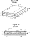
Figures 1A and 1B illustrate an example of asimple OET device 100 for manipulatingobjects 108 in aliquid medium 106 in achamber 104, which can be between anupper electrode 112,sidewalls 114,photoconductive material 116, and alower electrode 124. As shown, apower source 126 can be applied to theupper electrode 112 and thelower electrode 124.Figure 1C shows a simplified equivalent circuit in which the impedance of themedium 106 in thechamber 104 is represented byresistor 142 and the impedance of thephotoconductive material 116 is represented by the resistor 144. -
Photoconductive material 116 is substantially resistive unless illuminated by light. While not illuminated, the impedance of the photoconductive material 116 (and thus the resistor 144 in the equivalent circuit ofFigure 1C ) is greater than the impedance of the medium 106 (and thus theresistor 142 inFigure 1C ). Most of the voltage drop from the power applied to theelectrodes Figure 1C ) rather than across the medium 106 (and thusresistor 142 in the equivalent circuit ofFigure 1C ). - A
virtual electrode 132 can be created at aregion 134 of thephotoconductive material 116 by illuminating theregion 134 withlight 136. When illuminated withlight 136, thephotoconductive material 116 becomes electrically conductive, and the impedance of thephotoconductive material 116 at theilluminated region 134 drops significantly. The illuminated impedance of the photoconductive material 116 (and thus the resistor 144 in the equivalent circuit ofFigure 1C ) at theilluminated region 134 can thus be significantly reduced, for example, to less than the impedance of themedium 106. At theilluminated region 134, most of thevoltage drop 126 is now across the medium 106 (resistor 142 inFigure 1C ) rather than the photoconductive material 116 (resistor 144 inFigure 1C ). The result is a non-uniform electrical field in themedium 106 generally from theilluminated region 134 to a corresponding region on theupper electrode 112. The non-uniform electrical field can result in a DEP force on anearby object 108 in themedium 106. - Virtual electrodes like
virtual electrode 132 can be selectively created and moved in any desired pattern or patterns by illuminating thephotoconductive material 116 with different and moving patterns of light.Objects 108 in themedium 106 can thus be selectively manipulated (e.g., moved) in themedium 106. - Generally speaking, the unilluminated impedance of the
photoconductive material 116 must be greater than the impedance of themedium 106, and the illuminated impedance of thephotoconductive material 116 must be less than the impedance of themedium 106. As can be seen, the lower the impedance of themedium 106, the lower the required illuminated impedance of thephotoconductive material 116. Due to such factors as the natural characteristics of typical photoconductive materials and a limit to the intensity of thelight 136 that can, as a practical matter, be directed onto aregion 134 of thephotoconductive material 116, there is a lower limit to the illuminated impedance that can, as a practical matter, be achieved. It can thus be difficult to use a relativelylow impedance medium 106 in an OET device like theOET device 100 ofFigures 1A and 1B . -
US Patent No. 7,956,339 addresses the foregoing by using phototransistors in a layer like thephotoconductive material 116 ofFigures 1A and 1B selectively to establish, in response to light likelight 136, low impedance localized electrical connections from thechamber 104 to thelower electrode 124. The impedance of an illuminated phototransistor can be less than the illuminated impedance of thephotoconductive material 116, and an OET device configured with phototransistors can thus be utilized with alower impedance medium 106 than the OET device ofFigures 1A and 1B . Phototransistors, however, do not provide an efficient solution to the above-discussed short comings of prior art OET devices. For example, in phototransistors, the light absorption and electrical amplification for impedance modulation are typically coupled and thus constrained in independent optimization of both. - Embodiments of the present invention address the foregoing problems and/or other problems in prior art OET devices as well as provide other advantages.
- According to a first aspect of the invention, there is provided a microfluidic apparatus as set out in claim 1.
- According to a second aspect of the invention, there is provided a process of controlling a micro-fluidic device, the process as set out in claim 16.
- In some embodiments, a microfluidic apparatus can include a circuit substrate, a chamber, a first electrode, a second electrode, a switch mechanism, and photosensitive elements. Dielectrophoresis (DEP) electrodes can be located at different locations on a surface of the circuit substrate. The chamber can be configured to contain a liquid medium on the surface of the circuit substrate. The first electrode can be in electrical contact with the medium, and the second electrode can be electrically insulated from the medium. The switch mechanisms can each be located between a different corresponding one of the DEP electrodes and the second electrode, and each switch mechanism can be switchable between an off state in which the corresponding DEP electrode is deactivated and an on state in which the corresponding DEP electrode is activated. The photosensitive elements can each be configured to provide an output signal for controlling a different corresponding one of the switch mechanisms in accordance with a beam of light directed onto the photosensitive element.
- In some embodiments, a process of controlling a microfluidic device can include applying alternating current (AC) power to a first electrode and a second electrode of the microfluidic device, where the first electrode is in electrical contact with a medium in a chamber on an inner surface of a circuit substrate of the microfluidic device, and the second electrode is electrically insulated from the medium. The process can also include activating a dielectrophoresis (DEP) electrode on the inner surface of the circuit substrate, where the DEP electrode is one of a plurality of DEP electrodes on the inner surface that are in electrical contact with the medium. The DEP electrode can be activated by directing a light beam onto a photosensitive element in the circuit substrate, providing, in response to the light beam, an output signal from the photosensitive element, and switching, in response to the output signal, a switch mechanism in the circuit substrate from an off state in which the DEP electrode is deactivated to an on state in which the DEP electrode is activated.
- In some embodiments, a microfluidic apparatus can include a circuit substrate and a chamber configured to contain a liquid medium disposed on an inner surface of the circuit substrate. The microfluidic apparatus can also include means for activating a dielectrophoresis (DEP) electrode at a first region of the inner surface of the circuit substrate in response to a beam of light directed onto a second region of the inner surface, where the second region is spaced apart from the first region.
-
-
Figure 1A illustrates a perspective view of a simplified prior art OET device. -
Figure 1B shows a side, cross-sectional view of the OET device ofFigure 1A . -
Figure 1C is an equivalent circuit diagram of the OET device ofFigure 1A . -
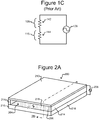
Figure 2A is a perspective view of a simplified OET device according to some embodiments of the invention. -
Figure 2B shows a side, cross-sectional view of the OET device ofFigure 2A . -
Figure 2C is a top view of an inner surface of a circuit substrate of the OET device ofFigure 2A . -
Figure 3 is an equivalent circuit diagram of the OET device ofFigure 2A . -
Figure 4 shows a partial, side cross-sectional view of an OET device in which the photosensitive element ofFigures 2A-2C comprises a photodiode and the switch mechanism comprises a transistor according to some embodiments of the invention. -
Figure 5 shows a partial, side cross-sectional view of an OET device in which the photosensitive element ofFigures 2A-2C comprises a photodiode and the switch mechanism comprises an amplifier according to some embodiments of the invention. -
Figure 6 shows a partial, side cross-sectional view of an OET device in which the photosensitive element ofFigures 2A-2C comprises a photodiode and the switch mechanism comprises an amplifier and a switch according to some embodiments of the invention. -
Figure 7 is a partial, side cross-sectional view of an OET device having a color detector element according to some embodiments of the invention. -
Figure 8 illustrates a partial, side cross-sectional view of an OET device with an indicator element for indicating whether a DEP electrode is activated according to some embodiments of the invention. -
Figure 9 illustrates a partial, side cross-sectional view of an OET device with multiple power supplies connected to multiple additional electrodes according to some embodiments of the invention. -
Figure 10 illustrates an example of a process of operating an OET device like the devices ofFigures 2A-2C and4-9 according to some embodiments of the invention. - This specification describes exemplary embodiments and applications of the invention. The invention, however, is not limited to these exemplary embodiments and applications or to the manner in which the exemplary embodiments and applications operate or are described herein. Moreover, the Figures may show simplified or partial views, and the dimensions of elements in the Figures may be exaggerated or otherwise not in proportion for clarity. In addition, as the terms "on," "attached to," or "coupled to" are used herein, one element (e.g., a material, a layer, a substrate, etc.) can be "on," "attached to," or "coupled to" another element regardless of whether the one element is directly on, attached, or coupled to the other element or there are one or more intervening elements between the one element and the other element. Also, directions (e.g., above, below, top, bottom, side, up, down, under, over, upper, lower, horizontal, vertical, "x," "y," "z," etc.), if provided, are relative and provided solely by way of example and for ease of illustration and discussion and not by way of limitation. In addition, where reference is made to a list of elements (e.g., elements a, b, c), such reference is intended to include any one of the listed elements by itself, any combination of less than all of the listed elements, and/or a combination of all of the listed elements.
- As used herein, "substantially" means sufficient to work for the intended purpose. The term "ones" means more than one.
- In some embodiments of the invention, dielectrophoresis (DEP) electrodes can be defined in an optoelectronic tweezers (OET) device by switch mechanisms that connect electrically conductive terminals on an inner surface of a circuit substrate to a power electrode. The switch mechanisms can be switched between an "off" state in which the corresponding DEP electrode is not active and an "on" state in which the corresponding DEP electrode is active. The state of each switch mechanism can be controlled by a photosensitive element connected to but spaced apart from the switch mechanism.
Figures 2A-2C illustrate an example of such amicrofludic OET device 200 according to some embodiments of the invention. - As shown in
Figures 2A-2C , theOET device 200 can comprise achamber 204 for containing aliquid medium 206. TheOET device 200 can also comprise acircuit substrate 216, afirst electrode 212, asecond electrode 224, and an alternating current (AC)power source 226, which can be connected to thefirst electrode 212 and thesecond electrode 224. - The
first electrode 212 can be positioned in thedevice 200 to be in electrical contact with (and thus electrically connected to) the medium 206 in thechamber 204. In some embodiments, all or part of thefirst electrode 212 can be transparent to light so thatlight beams 250 can pass through thefirst electrode 212. In contrast to thefirst electrode 212, thesecond electrode 224 can be positioned in thedevice 200 to be electrically insulated from the medium 206 in thechamber 204. For example, as shown, thecircuit substrate 216 can comprise thesecond electrode 224. For example, thesecond electrode 224 can comprise one or more metal layers on or in thecircuit substrate 216. Although illustrated inFigure 2B as a layer inside thecircuit substrate 216, thesecond electrode 224 can alternatively be part of a metal layer on thesurface 218 of thecircuit substrate 216. Regardless, such a metal layer can comprise a plate, a pattern of metal traces, or the like. - The
circuit substrate 216 can comprise a material that has a relatively high electrical impedance. For example, the impedance of thecircuit substrate 216 generally can be greater than the electrical impedance of the medium 206 in thechamber 204. For example, the impedance of thecircuit substrate 216 can be two, three, four, five, or more times the impedance of the medium 206 in thechamber 204. In some embodiments, thecircuit substrate 216 can comprise a semiconductor material, which undoped, has a relatively high electrical impedance. - As shown in
Figure 2B , thecircuit substrate 216 can comprise circuit elements interconnected to form electric circuits (e.g.,control modules 240, which are discussed below). For example, such circuits can be integrated circuits formed in the semiconductor material of thecircuit substrate 216. Thecircuit substrate 216 can thus comprise multiple layers of different materials such as undoped semiconductor material, doped regions of the semiconductor material, metal layers, electrically insulating layers, and the like such as is generally known in the field of forming microelectronic circuits integrated into semiconductor material. For example, as shown inFigure 2B , thecircuit substrate 216 can comprise thesecond electrode 224, which can be part of one or more metal layers of thecircuit substrate 216. In some embodiments, thecircuit substrate 216 can comprise an integrated circuit corresponding to any of many known semiconductor technologies such as complementary metal-oxide semiconductor (CMOS) integrated circuit technology, bi-polar integrated circuit technology, or bi-MOS integrated circuit technology. - As shown in
Figures 2B and 2C , thecircuit substrate 216 can comprise aninner surface 218, which can be part of thechamber 204. As also shown,DEP electrodes 232 can be located on thesurface 218. As best seen inFigure 2C , theDEP electrodes 232 can be distinct one from another. For example, theDEP electrodes 232 are not directly connected to each other electrically. - As illustrated in
Figures 2B and 2C , eachDEP electrode 232 can comprise an electrically conductive terminal, which can be in any of many different sizes, shapes, and locations on thesurface 218. For example, as illustrated by theDEP electrodes 232 in the middle column ofDEP electrodes 232 ofFigure 2C , the conductive terminal of eachDEP electrode 232 can be spaced apart from a correspondingphotosensitive element 242. As another example, and as illustrated by the left and right columns ofDEP electrodes 232 inFigure 2C , the conductive terminal of eachDEP electrode 232 can be disposed around (entirely as shown or partially (not shown)) and extend away from a correspondingphotosensitive element 242, and those terminals can comprise an opening 234 (e.g., a window) through which alight beam 250 can pass to strike thephotosensitive element 242. Alternatively, the terminals ofsuch DEP electrodes 232 can be transparent to light and thus can cover a correspondingphotosensitive element 242 without having anopening 234. Although theDEP electrodes 232 are illustrated inFigures 2B and 2C (and in other figures) as comprising an electrically conductive terminal, one or more of theDEP electrodes 232 can alternatively comprise merely a region of thesurface 218 of thecircuit substrate 216 where one of theswitch mechanisms 246 is in electrical contact with the medium 206 in thechannel 204. Regardless, as can be seen inFigure 2B , theinner surface 218 can be part of thechamber 204, and the medium 206 can be disposed on theinner surface 218 and theDEP electrodes 232. - As noted above, the
circuit substrate 216 can comprise electric circuit elements interconnected to form electrical circuits. As illustrated inFigure 2B , such circuits can comprisecontrol modules 240, which can comprise aphotosensitive element 242,control circuitry 244, and aswitch mechanism 246. - As shown in
Figure 2B , eachswitch mechanism 246 can connect one of theDEP electrodes 232 to thesecond electrode 224. In addition, eachswitch mechanism 246 can be switchable between at least two different states. For example, theswitch mechanism 246 can be switched between an "off" state and an "on" state. In the "off" state, theswitch mechanism 246 does not connect thecorresponding DEP electrode 232 to thesecond electrode 224. Put another way, theswitch mechanism 246 provides only a high impedance electrical path from thecorresponding DEP electrode 232 to thesecond electrode 224. Moreover, thecircuit substrate 216 does not otherwise provide an electrical connection from thecorresponding DEP electrode 232 to thesecond electrode 224, and thus there is nothing but a high impedance connection from thecorresponding DEP electrode 232 to thesecond electrode 224 while theswitch mechanism 246 is in the off state. In the on state, theswitch mechanism 246 electrically connects thecorresponding DEP electrode 232 to thesecond electrode 224 and thus provides a low impedance path from thecorresponding DEP electrode 232 to thesecond electrode 224. The high impedance between thecorresponding DEP electrode 232 while theswitch mechanism 246 is in the off state can be a greater impedance than the medium 206 in thechamber 204, and the low impedance connection from thecorresponding DEP electrode 232 to thesecond electrode 224 provided by theswitch mechanism 246 in the on state can have a lesser impedance than the medium 206. The foregoing is illustrated inFigure 3 . -
Figure 3 illustrates an equivalent circuit in which theresistor 342 represents the impedance of the medium 206 in thechamber 204 and theresistor 344 represents the impedance of a switch mechanism 246-and thus the impedance between one of theDEP electrodes 232 on theinner surface 218 of thecircuit substrate 216 and thesecond electrode 224. As noted, the impedance (represented by resistor 344) between acorresponding DEP electrode 232 and thesecond electrode 224 is greater than the impedance (represented by resistor 342) of the medium 206 while theswitch mechanism 246 is in the off state, but the impedance (represented by resistor 344) between acorresponding DEP electrode 232 and thesecond electrode 224 becomes less than the impedance (represented by resistor 342) of the medium 206 while theswitch mechanism 246 is in the on state. Turning aswitch mechanism 246 on thus creates a non-uniform electrical field in the medium 206 generally from theDEP electrode 232 to a corresponding region on theelectrode 212. The non-uniform electrical field can result in a DEP force on a nearby micro-object 208 (e.g., a micro-particle or biological object such as a cell or the like) in the medium 206. Because neither theswitch mechanism 246 nor the portion of thecircuit substrate 216 between theDEP electrode 232 and thesecond electrode 224 need be a photosensitive circuit element or even comprise photoconductive material, theswitch mechanism 246 can provide a significantly lower impedance connection from aDEP electrode 232 to thesecond electrode 224 than in prior art OET devices, and theswitch mechanism 246 can be much smaller than phototransistors used in prior art OET devices. - In some embodiments, the impedance of the off state of the
switch mechanism 246 can be two, three, four, five, ten, twenty, or more times the impedance of the on state. Also, in some embodiments, the impedance of the off state of theswitch 246 can be two, three, four, five, ten, or more times the impedance of the medium 206, which can be two, three, four, five, ten, or more times the impedance of the on state of theswitch mechanism 246. - Even though the
switch mechanism 246 need not be photoconductive, thecontrol module 240 can be configured such that theswitch mechanism 246 is controlled by a beam oflight 250. Thephotosensitive element 242 of eachcontrol module 240 can be a photosenstive circuit element that is activated (e.g., turned on) and deactivated (e.g., turned off) in response to a beam oflight 250. Thus, for example, as shown inFigure 2B , thephotosensitive element 242 can be disposed at a region on theinner surface 218 of thecircuit substrate 216. A beam of light 250 (e.g., from a light source (not shown) such as a laser or other light source) can be selectively directed onto thephotosensitive element 242 to activate theelement 242, and the beam oflight 250 thereafter can be removed from thephotosensitive element 242 to deactivate theelement 242. An output of thephotosensitive element 242 can be connected to a control input of theswitch mechanism 246 to switch theswitch mechanism 246 between the off and on states. - In some embodiments, as shown in
Figure 2B ,control circuitry 244 can connect thephotosensitive element 242 to theswitch mechanism 246. Thecontrol circuitry 244 can be said to "connect" the output of thephotosensitive element 242 to theswitch mechanism 246, and thephotosensitive element 242 can be said to be connected to and/or controlling theswitch mechanism 246, as long as thecontrol circuitry 244 utilizes the output of thephotosensitive element 242 to control the impedance state of theswitch mechanism 246. In some embodiments, however, thecontrol circuitry 244 need not be present, and thephotosensitive element 242 can be connected directly to theswitch mechanism 246. Regardless, the state of theswitch mechanism 246 can be controlled by the beam oflight 250 on thephotosensitive element 242. For example, the state of theswitch mechanism 246 can be controlled by the presence or absence of the beam oflight 250 on thephotosensitive element 242. - The
control circuitry 244 can comprise analog circuitry, digital circuitry, a digital memory and digital processor operating in accordance with machine readable instructions (e.g., software, firmware, microcode, or the like) stored in the memory, or a combination of one or more of the forgoing. In some embodiments, thecontrol circuitry 244 can comprise one or more digital latches (not shown), which can latch a pulsed output of thephotosensitive element 242 caused by a pulse of alight beam 250 directed onto thephotosensitive element 242. Thecontrol circuitry 244 can thus be configured (e.g., with one or more latches) to toggle the state of theswitch mechanism 246 between the off state and the on state each time a pulse of thelight beam 250 is directed onto thephotosensitive element 242. - For example, a first pulse of the
light beam 250 on the photosensitive element 242-and thus a first pulse of a positive signal output by the photosensitive element 242-can cause thecontrol circuitry 244 to put theswitch mechanism 246 into the on state. Moreover, thecontrol circuitry 244 can maintain theswitch mechanism 246 in the on state even after the pulse of thelight beam 250 is removed from thephotosensitive element 242. Thereafter, the next pulse of thelight beam 250 on the photosensitive element 242-and thus the next pulse of the positive signal output by the photosensitive element 242-can cause thecontrol circuitry 244 to toggle theswitch mechanism 246 to the off state. Subsequent pulses of thelight beam 250 on the photosensitive element 242-and thus subsequent pulses of the positive signal output by the photosensitive element 242-can toggle theswitch mechanism 246 between the off and the on states. - As another example, the
control circuitry 244 can control theswitch mechanism 246 in response to different patterns of pulses of thelight beam 250 on thephotosensitive element 242. For example, thecontrol circuitry 244 can be configured to set theswitch mechanism 246 to the off state in response to a sequence of n pulses of thelight beam 250 on the photosensitive element 242 (and thus n corresponding pulses of a positive signal from thephotosensitive element 242 to the control circuitry 244) having a first characteristic and set theswitch mechanism 246 to the on state in response to a sequence of k pulses (and thus k corresponding pulses of a positive signal from thephotosensitive element 242 to the control circuitry 244) having a second characteristic, wherein n and k can be equal or unequal integers. Examples of the first characteristic and the second characteristic can include the following: the first characteristic can be that the n pulses occur at a first frequency, and the second characteristic can be that the k pulses occur at a second frequency that is different than the first frequency. As another example, the pulses can have different widths (e.g., a short width and a long width) like, for example, Morris Code. The first characteristic can be a particular pattern of n short and/or long width pulses of thelight beam 250 that constitutes a predetermined off-state code, and the second characteristic can be a different pattern of k short and/or long width pulses of thelight beam 250 that constitutes a predetermined on-state code. Indeed, the foregoing examples can be configured to switch theswitch mechanism 246 between more than two states. Thus, theswitch mechanism 246 can have more and/or different states than merely an on state and an off state. - As yet another example, the
control circuitry 244 can be configured to control the state of theswitch mechanism 246 in accordance with a characteristic of the light beam 250 (and thus the corresponding pulse of a positive signal from thephotosensitive element 242 to the control circuitry 244) other than merely the presence or absence of thebeam 250. For example, thecontrol circuitry 244 can control theswitch mechanism 246 in accordance with the brightness of the beam 250 (and thus the level of a corresponding pulse of a positive signal from thephotosensitive element 242 to the control circuitry 244). Thus, for example, a detected brightness level of the beam 250 (and thus a level of a corresponding pulse of a positive signal from thephotosensitive element 242 to the control circuitry 244) that is greater than a first threshold but less than a second threshold can cause thecontrol circuitry 244 to set theswitch mechanism 246 to the off state, and a detected brightness level of the beam 250 (and thus a level of a corresponding pulse of a positive signal from thephotosensitive element 242 to the control circuitry 244) that is greater than the second threshold can cause thecontrol circuitry 244 to set theswitch mechanism 246 to the on state. In some embodiments, there can be a two, five, ten, or more times difference between the first brightness level and the second brightness level.Figure 7 , which is discussed below, illustrates an example in which thecontrol circuitry 244 can control the state of theswitching mechanism 246 in accordance with the color of thelight beam 250. Again, the foregoing examples can be configured to switch theswitch mechanism 246 between more than two states. - As still another example, the
control circuitry 244 can be configured to control the state of theswitch mechanism 246 in accordance with any combination of the foregoing characteristics of thelight beam 250 or multiple characteristics of thelight beam 250. For example, thecontrol circuitry 244 can be configured to set theswitching mechanism 246 to the off state in response to a sequence of n pulses within a particular frequency band of thelight beam 250 and to the on state in response to the brightness of thelight beam 250 exceeding a predetermined threshold. - The
control module 240 is thus capable of controlling aDEP electrode 232 on theinner surface 218 of thecircuit substrate 218 in accordance with the presence or absence of a beam oflight 250, a characteristic of thelight beam 250, or a characteristic of a sequence of pulses of thelight beam 250 at a different region (e.g., corresponding to the location of the photosensitive element 242) of theinner surface 218, where the different region is spaced apart from thefirst DEP electrode 232. Thephotosensitive element 242, thecontrol circuitry 244, and/or theswitch element 246 are thus examples of means for activating aDEP electrode 232 at a first region (e.g., any portion of aDEP electrode 232 not disposed over a corresponding photosensitive element 242) on an inner surface (e.g., 218) of a circuit substrate (e.g., 216) in response to a beam of light (e.g., 250) directed onto a second region (e.g., corresponding to the photosensitive element 242) of theinner surface 218, where the second region is spaced apart on theinner surface 218 from the first region. - As illustrated in
Figures 2B and 2C , there can be multiple (e.g., many)control modules 240 each configured to control adifferent DEP electrode 232 on theinner surface 218 of the circuit substrate. TheOET device 200 ofFigures 2A-2C can thus comprise many DEP electrodes in the form ofDEP electrodes 232 each controllable by directing or removing a beam oflight 250 on aphotosensitive element 242. Moreover, at least a portion of eachDEP electrode 232 can be spaced apart on theinner surface 218 from the corresponding photosensitive element 242-and thus the region on the inner surface where light 250 is directed-that controls the state of theDEP electrode 232. - The illustrations in
Figures 2A-2C are examples only, and variations are contemplated. For example, as noted, there need not becontrol circuitry 244, and thephotosensitive elements 242 can be connected directly to theswitch mechanisms 246. As another example, eachcontrol module 240 need not includecontrol circuitry 244. Instead, one or more instances of thecontrol circuitry 244 can be shared among multiplephotosensitive elements 242 andswitch mechanisms 246. As yet another example,DEP electrodes 232 need not include distinct terminals on thesurface 218 of thecircuit substrate 216 but can instead be regions of thesurface 218 where theswitch mechanisms 246 are in electrical contact with the medium 206 in thechamber 204. -
Figures 4-6 illustrate various embodiments and exemplary configurations of thephotosensitive element 242 and theswitch mechanism 246 ofFigures 2A-2C . -
Figure 4 illustrates anOET device 400 that can be similar to theOET device 200 ofFigures 2A-2C except that thephotosensitive element 242 can comprise aphotodiode 442 and theswitch mechanism 246 can comprise atransistor 446. Otherwise, theOET device 400 can be the same as theOET device 200, and indeed, like numbered elements inFigures 2A-2C and4 can be the same. As noted above, thecircuit substrate 216 can comprise a semiconductor material, and thephotodiode 442 andtransistor 446 can be formed in layers of thecircuit substrate 216 as is known in the field of semiconductor manufacturing. - An
input 444 of thephotodiode 442 can be biased with a direct current (DC) power source (not shown). Thephotodiode 442 can be configured and positioned so that alight beam 250 directed at a location on theinner surface 218 that corresponds to thephotodiode 442 can activate thephotodiode 442, causing thephotodiode 442 to conduct and thus output a positive signal to thecontrol circuitry 244. Removing thelight beam 250 can deactivate thephotodiode 442, causing thephotodiode 442 to stop conducting and thus output a negative signal to thecontrol circuitry 244. - The
transistor 446 can be any type of transistor, but need not be a phototransistor. For example, thetransistor 446 can be a field effect transistor (FET) (e.g., a complementary metal oxide semiconductor (CMOS) transistor), a bipolar transistor, or a bi-MOS transistor. - If the
transistor 446 is a FET transistor as shown inFigure 4 , the drain or source can be connected to theDEP electrode 232 on theinner surface 218 of thecircuit substrate 216 and the other of the drain or source can be connected to thesecond electrode 224. The output of thephotodiode 442 can be connected (e.g., by the control circuitry 244) to the gate of thetransistor 446. Alternatively, the output of thephotodiode 442 can be connected directly to the gate of thetransistor 446. Regardless, thetransistor 446 can be biased so that the signal provided to the gate turns thetransistor 446 off or on. - If the
transistor 446 is a bipolar transistor, the collector or emitter can be connected to theDEP electrode 232 on theinner surface 218 of thecircuit substrate 216 and the other of the collector or emitter can be connected to thesecond electrode 224. The output of thephotodiode 442 can be connected (e.g., by the control circuitry 244) to the base of thetransistor 446. Alternatively, the output of thephotodiode 442 can be connected directly to the base of thetransistor 446. Regardless, thetransistor 446 can be biased so that the signal provided to the base turns thetransistor 446 off or on. - Regardless of whether the
transistor 446 is a FET transistor or a bipolar transistor, thetransistor 446 can function as discussed above with respect to theswitch mechanism 226 ofFigures 2A-2C . That is, turned on, thetransistor 446 can provide a low impedance electrical path from theDEP electrode 232 to thesecond electrode 224 as discussed above with respect to theswitch mechanism 226 inFigures 2A-2C . Conversely, turned off, thetransistor 446 can provide a high impedance electrical path from theDEP electrode 232 to thesecond electrode 224 as described above with respect to theswitch mechanism 226. -
Figure 5 illustrates anOET device 500 that can be similar to theOET device 200 ofFigures 2A-2C except that thephotosensitive element 242 comprises the photodiode 442 (which can be the same as described above with respect toFigure 4 ) and theswitch mechanism 246 comprises an amplifier 546, which need not be photoconductive. Otherwise, theOET device 500 can be the same as theOET device 200, and indeed, like numbered elements inFigures 2A-2C and5 can be the same. As noted above, thecircuit substrate 216 can comprise a semiconductor material, and the amplifier 546 can be formed in layers of thecircuit substrate 216 as is known in the field of semiconductor processing. - The amplifier 546 can be any type of amplifier. For example, the amplifier 546 can be an operational amplifier, one or more transistors configured to function as an amplifier, or the like. As shown, the
control circuitry 244 can utilize the output of thephotodiode 442 to control the amplification level of the amplifier 546. For example,control circuitry 244 can control the amplifier 546 to function as discussed above with respect to theswitch mechanism 226 ofFigures 2A-2C . That is, in the absence of thelight beam 250 on the photodiode 442 (and thus the absence of an output from the photodiode 442), thecontrol circuitry 244 can turn the amplifier 546 off or set the gain of the amplifier 546 to zero, effectively causing the amplifier 546 to provide a high impedance electrical connection from theDEP electrode 232 to thesecond electrode 224 as discussed above with respect to theswitch mechanism 246. Conversely, the presence of thelight beam 250 on the photodiode 442 (and thus an output from the photodiode 442) can cause thecontrol circuitry 244 to turn the amplifier 546 on or set the gain of the amplifier 546 to a non-zero value, effectively causing the amplifier 546 to provide a low impedance electrical connection from theDEP electrode 232 to thesecond electrode 224 as discussed above with respect to theswitch mechanism 246. - The
OET device 600 ofFigure 6 can be similar to theOET device 500 ofFigure 5 except that the switch mechanism 246 (seeFigures 2A-2C ) can comprise aswitch 604 in series with anamplifier 602. Theswitch 604 can comprise any kind of electrical switch including a transistor such astransistor 442 ofFigure 4 . Theamplifier 602 can be like the amplifier 546 offigure 5 . Theswitch 604 andamplifier 602 can be formed in thecircuit substrate 216 generally as discussed above. - The
control circuitry 244 can be configured to control whether theswitch 604 is open or closed in accordance with the output of thephotodiode 442. Alternatively, the output of thephotodiode 442 can be connected directly to theswitch 604. Regardless, when theswitch 604 is open, theswitch 604 andamplifier 602 can provide a high impedance electrical connection from theDEP electrode 232 to thesecond electrode 224 as discussed above. Conversely, while theswitch 604 is closed, theswitch 604 andamplifier 602 can provide a low impedance electrical connection from theDEP electrode 232 to thesecond electrode 224 as discussed above. -
Figure 7 illustrates a partial, side cross-sectional view of an OET device 700 that can be like thedevice 200 ofFigures 2A-2C except that each of one or more (e.g., all) of thephotosensitive elements 242 can be replaced with a color detector element 710. One color detector element 710 is shown inFigure 7 , but each of thephotosensitive elements 242 inFigures 1A-1C can be replaced with such an element 710. Thecontrol module 740 inFigure 7 can otherwise be like thecontrol module 240 inFigures 1A-1C , and like numbered elements inFigures 1A-1C and7 are the same. - As shown, a color detector element 710 can comprise a plurality of
color photo detectors 702, 704 (two are shown but there can be more). Eachpass color detector control circuitry 244 in response to a different color of thelight beam 250. For example, thephoto detector 702 can be configured to provide a positive signal to thecontrol circuitry 244 when alight beam 250 of a first color is directed onto thephoto detectors photo detector 704 can be configured to provide a positive signal to thecontrol circuitry 244 when thelight beam 250 is a second color, which can be different than the first color. - As shown, each
photo detector color filter 706 and a photosensitive element 708. Eachfilter 706 can be configured to pass only a particular color. For example, thefilter 706 of thefirst photo detector 702 can pass substantially only a first color, and thefilter 706 of thesecond photo detector 704 can pass substantially only a second color. The photosensitive elements 708 can both be similar to or the same as the photosensitive element 242 inFigures 2A-2C as discussed above. - The configurations of the
color photo detectors Figure 7 are an example only, and variations are contemplated. For example, rather than comprising afilter 706 and a photosensitive element 708, one or both of thecolor photo detectors - Regardless, the
control circuitry 244 can be configured to set theswitch mechanism 246 to one state (e.g., the on state) in response to abeam 250 pulse of the first color and to set theswitch mechanism 246 to another state (e.g., the off state) in response to abeam 250 pulse of the second color. As mentioned, the color detector element 710 can comprise more than twocolor photo detectors control circuitry 244 can thus be configured to switch theswitch mechanism 246 among more than two different states. -
Figure 8 is a partial, side cross-sectional view of an OET device 800 that can be like thedevice 200 ofFigures 2A-2C except that eachcontrol module 840 can further include anindicator element 802. That is, the device 800 can be like thedevice 200 ofFigures 2A-2C except acontrol module 840 can replace eachcontrol module 240, and there can thus be anindicator element 802 associated with eachDEP electrode 232. Otherwise, the device 800 can be likedevice 200 inFigures 2A-2C , and like numbered elements inFigures 2A-2C and8 are the same. - As shown, the
indicator element 802 can be connected to the output of thecontrol circuitry 244, which can be configured to set theindicator element 802 to different states each of which corresponds to one of the possible states of theswitch mechanism 246. Thus, for example, thecontrol circuitry 244 can turn theindicator element 802 on while theswitch mechanism 246 is in the on state and turn theindicator element 802 off while theswitch mechanism 246 is in the off state. In the foregoing example, theindicator element 802 can thus be on while its associatedDEP electrode 232 is activated and off while theDEP electrode 232 is not activated. - The
indicator element 802 can provide a visional indication (e.g., emit light 804) only when turned on. Non-limiting examples of theindicator element 802 include a light source such as a light emitting diode (which can be formed in the circuit substrate 216), a light bulb, or the like. As shown, theDEP electrode 232 can include a second opening 834 (e.g., window) for theindicator element 802. Alternatively, theindicator element 802 can be spaced away from theDEP electrode 232 and thus not covered by theDEP electrode 232, in which case, there need not be asecond window 834 in theDEP electrode 232. As yet another alternative, theDEP electrode 232 can be transparent to light, which case, there need not be asecond window 834 even if theDEP electrode 232 covers theindicator element 802. -
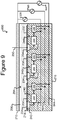
Figure 9 is a partial, side cross-sectional view of anOET device 900 that can be like thedevice 200 ofFigures 2A-2C except that thedevice 900 can comprise not only thesecond electrode 224 but one or more additional electrodes 924, 944 (two are shown but there can be one or more than two) and a corresponding plurality ofadditional power sources device 900 can be likedevice 200 inFigures 2A-2C , and like numbered elements inFigures 2A-2C and9 are the same. - As shown, each
switch mechanism 246 can be configured to connect electrically acorresponding DEP electrode 232 to one of theelectrodes switch mechanism 246 can thus be configured to selectively connect acorresponding DEP electrode 232 to thesecond electrode 224, a third electrode 924, or afourth electrode 944. Eachswitch mechanism 246 can also be configured to disconnect thefirst electrode 212 from all of theelectrodes - As also shown, the
power source 226 can be connected to (and thus provide power between) thefirst electrode 212 and thesecond electrode 224 as discussed above. Thepower source 926 can be connected to (and thus provide power between) thefirst electrode 212 and the third electrode 924, and thepower source 946 can be connected to (and thus provide power between) thefirst electrode 212 and thefourth electrode 944. - Each
electrode 924, 944 can be generally like thesecond electrode 224 as discussed above. For example, eachelectrode 924, 944 can be electrically insulated from the medium 206 in thechannel 204. As another example, eachelectrode 924, 944 can be part of a metal layer on thesurface 218 of or inside thecircuit substrate 216. Eachpower source power source 226 as discussed above. - The
power sources power source 226. For example, eachpower source switch mechanism 246 can thus switch the electrical connection from acorresponding DEP electrode 232 between an "off" state in which theDEP electrode 232 is not connected to any of theelectrodes DEP electrode 232 is connected to any one of theelectrodes - As another example of how the
power sources power source electrodes 224, 924 and thepower sources 226, 926 (but not theelectrode 944 and power source 946), thepower source 926 can provide power that is approximately (e.g., plus or minus ten percent) one hundred eighty (180) degrees out of phase with the power provided by thepower source 226. In such an embodiment, eachswitch mechanism 246 can be configured to switch between connecting acorresponding DEP electrode 232 to thesecond electrode 224 and the third electrode 924. Thedevice 900 can be configured so that thecorresponding DEP electrode 232 is activated (and thus turned on) while theDEP electrode 232 is connected to one of theelectrodes 224, 924 (e.g., 224) and deactivated (and thus turned off) while connected to the other of theelectrodes 224, 924 (e.g., 924). Such an embodiment can reduce leakage current from aDEP electrode 232 that is turned off as compared to thedevice 200 ofFigures 2A-2C . - It is noted that one or more of the following can comprise examples of means for activating a DEP electrode at a first region of the inner surface of the circuit substrate in response to a beam of light directed onto a second region of the inner surface, where the second region is spaced apart from the first region; activating means further for selectively activating a plurality of DEP electrodes at first regions of the inner surface of the circuit substrate in response to beams of light directed onto second regions of the inner surface, where the each second region is spaced apart from each the first region; activating means further for activating the DEP electrode in response to the beam of light having a first characteristic, and deactivating the DEP electrode in response to the beam of light having a second characteristic; activating means further for activating the DEP electrode in response to a sequence of n pulses of the beam of light having a first characteristic; and activating means further for deactivating the DEP electrode in response to a sequence of k pulses of the beam of light having a second characteristic: the photosensitive element 242, including the photodiode 442 and/or the multi-frequency photodetector 710; the control circuitry 244 configured in any manner described or illustrated herein; and/or the switch mechanism 246 include the transistor 446, the amplifier 546, and/or the amplifier 602 and switch 604.
-
Figure 10 illustrates aprocess 1000 for controlling DEP electrodes in a microfluidic OET device according to some embodiments of the invention. As shown, atstep 1002, a micro-fluidic OET device can be obtained. For example, any of themicrofluidic OET devices Figures 2A-2C and4-9 , or similar devices, can be obtained atstep 1002. Atstep 1004, AC power can be applied to electrodes of the device obtained atstep 1002. For example, as discussed above, theAC power source 226 can be connected to afirst electrode 212 that is in electrical contact with the medium 206 in thechamber 204 and asecond electrode 224 that is insulated from the medium 206. Atstep 1006, DEP electrodes of the device obtained atstep 1002 can be selectively activated and deactivated. For example, as discussed aboveDEP electrodes 232 can be selectively activated and deactivated by selectively directinglight beams 250 onto and removinglight beams 250 from photosensitive elements 242 (e.g., thephotodiode 442 ofFigures 4 ,5, and 6 ) to switch the impedance state of the switching mechanism 246 (e.g., thetransistor 446 ofFigure 4 , the amplifier 556 ofFigure 5 , and theswitch 602 andamplifier 604 ofFigure 5 ) as discussed above. - Although specific embodiments and applications of the invention have been described in this specification, these embodiments and applications are exemplary only, and many variations are possible.
Claims (19)
- A microfluidic apparatus (200, 400, 500, 600, 700, 800, 900) comprising:a circuit substrate (216) comprising a surface (218) and dielectrophoresis (DEP) electrodes (232) at different locations on said surface;a chamber (204) configured to contain a liquid medium (206) disposed on said surface of said circuit substrate;a first electrode (212) disposed to be in electrical contact with said medium;a second electrode (224) disposed to be electrically insulated from said medium;switch mechanisms (246) each disposed between, and electrically connecting, a different corresponding one of said DEP electrodes and said second electrode, wherein each said switch mechanism is configured to receive an output signal and switch, in response to said output signal, between an off state in which said corresponding DEP electrode is deactivated and an on state in which said corresponding DEP electrode is activated;photosensitive elements (242) each configured to provide said output signal to a different corresponding one of said switch mechanisms in accordance with a beam of light directed onto said photosensitive element.
- The apparatus of claim 1, wherein:while each said switch mechanism is in said off state, there is a high electrical impedance between said corresponding DEP electrode and said second electrode that is greater than an electrical impedance of said medium in said chamber, andin said on state, each said switch mechanism provides a low electrical impedance between said corresponding DEP electrode and said second electrode that is less than said electrical impedance of said medium.
- The apparatus of claim 2, wherein said high electrical impedance is at least two times greater than said low electrical impedance.
- The apparatus of claim 1, wherein:each said switch mechanism comprises an amplifier (546, 602) connecting said corresponding DEP electrode to said second electrode, andsaid circuit substrate comprises a semiconductor material in which circuit elements comprising said switch and said amplifier are formed; and optionally, wherein each said switch mechanism comprises a switch (604) in series with said amplifier (602).
- The apparatus of claim 1, wherein:each said switch mechanism comprises a transistor (446) connecting said corresponding DEP electrode to said second electrode, andsaid circuit substrate comprises a semiconductor material in which circuit elements comprising said transistor are formed and, optionally, said transistor is a field effect transistor or a bipolar transistor.
- The apparatus of claim 4 or 5, wherein:each said photosensitive element comprises a photodiode (442), andsaid circuit-substrate comprises a semiconductor material in which circuit elements comprising said photodiode are formed.
- The apparatus of claim 1 further comprising control circuits (244) each connecting a corresponding one of said photosensitive elements to a corresponding one of said switch mechanisms, wherein each said control circuit is configured to control whether said corresponding switch mechanism is in said off state or said on state in accordance with said output signal from said corresponding one of said photosensitive elements.
- The apparatus of claim 7, wherein the control circuit is configured to switch said corresponding switch element into an on state responsive to one output signal from said corresponding one of said photosensitive elements, wherein said corresponding one of said photosensitive elements generates said one output signal responsive to a pulse of said beam of light directed onto said photosensitive element.
- The apparatus of claim 8, wherein the control circuit is configured to switch said corresponding switch element into an off state responsive to one second signal output from said corresponding one of said photosensitive elements, wherein said corresponding one of said photosensitive elements generates said one second signal output responsive to a pulse of said beam of light directed onto said photosensitive element.
- The apparatus of claim 7, wherein each photosensitive element comprises a plurality of color photo detectors (702, 704), and wherein one or more signal outputs are generated responsive to said beam of light having a first colour and one or more second signal outputs are generated responsive to said beam of light having a second colour.
- The apparatus of claim 7, wherein the control circuit is further configured to:switch said corresponding switch element into an on state responsive to determining that the brightness of said signal output indicates that said beam of light directed onto said photosensitive element has a first characteristic; andswitch said corresponding switch element into an off state responsive to determining that the brightness of said second signal output indicates that said beam of light directed onto said photosensitive element has a second characteristic.
- The apparatus of claim 11, wherein said second characteristic comprises said beam of light having a brightness greater than a first threshold and less than a second threshold, and said first characteristic comprises said beam of light having a brightness greater than said second threshold.
- The apparatus of claim 7, wherein one or more signal outputs are generated responsive to n pulses of said beam of light, the one or more signal outputs are generated responsive to k pulses of said beam of light and said n pulses of said beam of light and said k pulses of said beam of light have a different frequency or pattern.
- The apparatus of claim 1 further comprising:a first AC power source (926) connected to said first electrode and said second electrode;a third electrode disposed to be electrically insulated from said second electrode and said medium in said chamber, anda second AC power source (946) connected to said first electrode and said third electrode;wherein each said switch mechanism is switchable between electrically connecting said corresponding DEP electrode to said second electrode or to said third electrode.
- The apparatus of claim 1 further comprising indicator elements (802) each configured to indicate whether a corresponding one of said switch mechanisms is in said on state or said off state.
- A process (1000) of controlling a microfluidic device comprising a circuit substrate and a chamber containing a liquid medium disposed on an inner surface of said circuit substrate, said process comprising:applying (1004) alternating current (AC) power to a first electrode and a second electrode of said microfluidic device, wherein said first electrode is in electrical contact with said medium and said second electrode is electrically insulated from said medium; andactivating (1002) a dielectrophoresis (DEP) electrode on said inner surface of said circuit substrate, wherein said DEP electrode is one of a plurality of DEP electrodes on said inner surface that are in electrical contact with said medium, said activating comprising:directing a light beam onto a photosensitive element in said circuit substrate,providing, in response to said light beam, an output signal from said photosensitive element,
andswitching, in response to said output signal, a switch mechanism in said circuit substrate from an off state in which said DEP electrode is deactivated to an on state in which said DEP electrode is activated. - The process of claim 16 further comprising deactivating said DEP electrode, wherein:said activating further comprises determining whether said output signal indicates that said light beam has a particular characteristic, and said switching comprises switching said switch mechanism from said off state to said on state only if said output signal indicates that said light beam has said particular characteristic; andsaid deactivating comprising:directing a second light beam onto said photosensitive element,providing, in response to said second light beam, a second output signal from said photosensitive element, andswitching said switch mechanism from said on state to said off state only if said second output signal indicates that said second light beam has a second particular characteristic.
- The process of claim 16 further comprising applying a second AC power to said third electrode of said microfluidic device, wherein said third electrode is electrically insulated from said medium and said first electrode and wherein said switching comprises switching said switch mechanism from said off state in which said switch mechanism connects said DEP electrode to said second electrode but not to said third electrode to said on state in which said switch mechanism connects said DEP electrode to said third electrode but not to said second electrode.
- The process of claim 18, wherein said applying said second AC power comprises applying said second AC power to said third electrode one-hundred and eighty degrees out of phase from said AC power applied to said second electrode.
Applications Claiming Priority (3)
| Application Number | Priority Date | Filing Date | Title |
|---|---|---|---|
| US201261724168P | 2012-11-08 | 2012-11-08 | |
| US14/051,004 US9403172B2 (en) | 2012-11-08 | 2013-10-10 | Circuit based optoelectronic tweezers |
| PCT/US2013/067564 WO2014074367A1 (en) | 2012-11-08 | 2013-10-30 | Circuit based optoelectronic tweezers |
Publications (3)
| Publication Number | Publication Date |
|---|---|
| EP2916954A1 EP2916954A1 (en) | 2015-09-16 |
| EP2916954A4 EP2916954A4 (en) | 2016-06-29 |
| EP2916954B1 true EP2916954B1 (en) | 2019-01-02 |
Family
ID=50621363
Family Applications (1)
| Application Number | Title | Priority Date | Filing Date |
|---|---|---|---|
| EP13853719.6A Active EP2916954B1 (en) | 2012-11-08 | 2013-10-30 | Circuit based optoelectronic tweezers |
Country Status (11)
| Country | Link |
|---|---|
| US (2) | US9403172B2 (en) |
| EP (1) | EP2916954B1 (en) |
| JP (1) | JP6293160B2 (en) |
| KR (1) | KR102141261B1 (en) |
| CN (2) | CN107252733B (en) |
| CA (2) | CA3101130C (en) |
| DK (1) | DK2916954T3 (en) |
| HK (3) | HK1213218A1 (en) |
| IL (1) | IL238451B (en) |
| SG (1) | SG11201600581SA (en) |
| WO (1) | WO2014074367A1 (en) |
Families Citing this family (52)
| Publication number | Priority date | Publication date | Assignee | Title |
|---|---|---|---|---|
| US9889445B2 (en) | 2013-10-22 | 2018-02-13 | Berkeley Lights, Inc. | Micro-fluidic devices for assaying biological activity |
| WO2015061506A1 (en) | 2013-10-22 | 2015-04-30 | Berkeley Lights, Inc. | Micro-fluidic devices for assaying biological activity |
| US10010882B2 (en) | 2013-10-22 | 2018-07-03 | Berkeley Lights, Inc. | Microfluidic devices having isolation pens and methods of testing biological micro-objects with same |
| US20150166326A1 (en) | 2013-12-18 | 2015-06-18 | Berkeley Lights, Inc. | Capturing Specific Nucleic Acid Materials From Individual Biological Cells In A Micro-Fluidic Device |
| US20150306599A1 (en) | 2014-04-25 | 2015-10-29 | Berkeley Lights, Inc. | Providing DEP Manipulation Devices And Controllable Electrowetting Devices In The Same Microfluidic Apparatus |
| US11192107B2 (en) | 2014-04-25 | 2021-12-07 | Berkeley Lights, Inc. | DEP force control and electrowetting control in different sections of the same microfluidic apparatus |
| US20150346148A1 (en) * | 2014-05-28 | 2015-12-03 | Agilent Technologies, Inc. | Method and Apparatus for Manipulating Samples Using Optoelectronic Forces |
| EP3180418A4 (en) * | 2014-08-15 | 2018-04-18 | The Regents of The University of California | Self-locking optoelectronic tweezer and its fabrication |
| CN110918142B (en) | 2014-12-08 | 2022-10-25 | 伯克利之光生命科技公司 | Directional flow actuated microfluidic structures in microfluidic devices and methods of using the same |
| DK3229958T3 (en) * | 2014-12-08 | 2020-11-30 | Berkeley Lights Inc | MICROFLUID DEVICE CONTAINING LATERAL / VERTICAL TRANSISTOR STRUCTURES, AND THE METHOD OF MANUFACTURE AND USE |
| WO2016094459A2 (en) | 2014-12-09 | 2016-06-16 | Berkeley Lights, Inc. | Automated detection and repositioning of micro-objects in microfluidic devices |
| KR20230125849A (en) | 2014-12-10 | 2023-08-29 | 버클리 라잇츠, 인크. | Systems for operating electrokinetic devices |
| WO2016094715A2 (en) | 2014-12-10 | 2016-06-16 | Berkeley Lights, Inc. | Movement and selection of micro-objects in a microfluidic apparatus |
| JP7051206B2 (en) | 2015-04-22 | 2022-04-11 | バークレー ライツ,インコーポレイテッド | Microfluidic cell culture |
| JP2018512875A (en) | 2015-04-22 | 2018-05-24 | バークレー ライツ,インコーポレイテッド | Freezing and storage of cells in microfluidic devices |
| WO2016172623A1 (en) | 2015-04-22 | 2016-10-27 | Berkeley Lights, Inc. | Manipulation of cell nuclei in a micro-fluidic device |
| SG10202011358PA (en) | 2015-04-22 | 2020-12-30 | Berkeley Lights Inc | Culturing station for microfluidic device |
| EP3096134B1 (en) * | 2015-05-21 | 2019-07-24 | Nokia Technologies Oy | An apparatus and method for providing a time varying voltage |
| US10799865B2 (en) | 2015-10-27 | 2020-10-13 | Berkeley Lights, Inc. | Microfluidic apparatus having an optimized electrowetting surface and related systems and methods |
| CN108472649B (en) | 2015-10-27 | 2022-01-14 | 伯克利之光生命科技公司 | Microfluidic devices with optimized electrowetting surfaces and related systems and methods |
| JP7296210B2 (en) | 2015-11-23 | 2023-06-22 | バークレー ライツ,インコーポレイテッド | In situ generated microfluidic separation structures, kits thereof, and methods of use thereof |
| DK3387438T3 (en) | 2015-12-08 | 2023-05-15 | Berkeley Lights Inc | MICROFLUIDIC DEVICES AND KITS AND METHODS OF USING THEREOF |
| EP3397586A4 (en) | 2015-12-30 | 2019-07-17 | Berkeley Lights, Inc. | Microfluidic devices for optically-driven convection and displacement, kits and methods thereof |
| WO2017117521A1 (en) | 2015-12-31 | 2017-07-06 | Berkeley Lights, Inc. | Tumor infilitrating cells engineered to express a pro-inflammatory polypeptide |
| JP6902548B2 (en) | 2016-01-15 | 2021-07-14 | バークレー ライツ,インコーポレイテッド | Manufacturing method of patient-specific anticancer therapeutic agent and its therapeutic method |
| CN109922885B (en) | 2016-03-16 | 2022-05-10 | 伯克利之光生命科技公司 | Methods, systems and apparatus for selection and generation of genome editing clones |
| CN115354025A (en) | 2016-03-17 | 2022-11-18 | 伯克利之光生命科技公司 | Selection and cloning of T lymphocytes in microfluidic devices |
| KR102451535B1 (en) | 2016-03-31 | 2022-10-05 | 버클리 라잇츠, 인크. | Nucleic acid stabilization reagents, kits, and methods of use thereof |
| US10675625B2 (en) | 2016-04-15 | 2020-06-09 | Berkeley Lights, Inc | Light sequencing and patterns for dielectrophoretic transport |
| KR102421818B1 (en) | 2016-04-15 | 2022-07-15 | 버클리 라잇츠, 인크. | Methods, systems and kits for in-pen assays |
| SG11201809539RA (en) | 2016-05-26 | 2018-12-28 | Berkeley Lights Inc | Covalently modified surfaces, kits, and methods of preparation and use |
| WO2018018017A1 (en) | 2016-07-21 | 2018-01-25 | Berkeley Lights, Inc. | Sorting of t lymphocytes in a microfluidic device |
| AU2017336164A1 (en) | 2016-10-01 | 2019-04-18 | Berkeley Lights, Inc. | DNA barcode compositions and methods of in situ identification in a microfluidic device |
| KR102560201B1 (en) | 2016-10-23 | 2023-07-27 | 버클리 라잇츠, 인크. | Methods for screening B cell lymphocytes |
| SG10202104487WA (en) | 2016-12-01 | 2021-05-28 | Berkeley Lights Inc | Apparatuses, systems and methods for imaging micro-objects |
| JP2019537157A (en) | 2016-12-01 | 2019-12-19 | バークレー ライツ,インコーポレイテッド | Automatic detection and relocation of minute objects by microfluidic devices |
| WO2018111765A1 (en) | 2016-12-12 | 2018-06-21 | xCella Biosciences, Inc. | Methods and systems for screening using microcapillary arrays |
| CN110546495B (en) | 2016-12-30 | 2022-11-01 | 加利福尼亚州立大学董事会 | Methods for selection and passage of genome editing T cells |
| KR20200026878A (en) | 2017-06-06 | 2020-03-11 | 지머젠 인코포레이티드 | HTP Genome Engineering Platform to Improve Fungal Strains |
| EP3721209B1 (en) | 2017-10-15 | 2024-02-07 | Berkeley Lights, Inc. | Methods for in-pen assays |
| WO2019232473A2 (en) | 2018-05-31 | 2019-12-05 | Berkeley Lights, Inc. | Automated detection and characterization of micro-objects in microfluidic devices |
| KR20210018219A (en) | 2018-06-06 | 2021-02-17 | 지머젠 인코포레이티드 | Modification of genes involved in signaling to control fungal morphology during fermentation and production |
| CN113348036A (en) * | 2018-11-19 | 2021-09-03 | 伯克利之光生命科技公司 | Microfluidic device with programmable switching elements |
| CN109622085B (en) * | 2019-01-31 | 2021-12-24 | 京东方科技集团股份有限公司 | Driving method and device of micro-fluidic chip and micro-fluidic system |
| WO2020168258A1 (en) * | 2019-02-15 | 2020-08-20 | Berkeley Lights, Inc. | Laser-assisted repositioning of a micro-object and culturing of an attachment-dependent cell in a microfluidic environment |
| CN114126762B (en) | 2019-04-30 | 2023-01-03 | 伯克利之光生命科技公司 | Methods for encapsulating and assaying cells |
| AU2020361681A1 (en) | 2019-10-10 | 2022-05-05 | 1859, Inc. | Methods and systems for microfluidic screening |
| TW202142856A (en) | 2019-11-17 | 2021-11-16 | 美商伯克利之光生命科技公司 | Systems and methods for analyses of biological samples |
| US11479779B2 (en) | 2020-07-31 | 2022-10-25 | Zymergen Inc. | Systems and methods for high-throughput automated strain generation for non-sporulating fungi |
| GB202109967D0 (en) * | 2021-07-09 | 2021-08-25 | Lightcast Discovery Ltd | Improvements in or relating to imaging microdroplets in a microfluidic device |
| US20240050948A1 (en) * | 2022-08-10 | 2024-02-15 | Cytoaurora Biotechnologies, Inc. | Contactless selection device, light sensing structure thereof, and biological particle selection apparatus |
| JP2024049813A (en) | 2022-09-29 | 2024-04-10 | 横河電機株式会社 | Dielectrophoresis Apparatus |
Family Cites Families (28)
| Publication number | Priority date | Publication date | Assignee | Title |
|---|---|---|---|---|
| ES2288760T3 (en) | 1996-04-25 | 2008-01-16 | Bioarray Solutions Ltd. | ELECTROCINETIC ASSEMBLY CONTROLLED BY LIGHT OF PARTICLES NEXT TO SURFACES. |
| US6294063B1 (en) | 1999-02-12 | 2001-09-25 | Board Of Regents, The University Of Texas System | Method and apparatus for programmable fluidic processing |
| US6942776B2 (en) | 1999-05-18 | 2005-09-13 | Silicon Biosystems S.R.L. | Method and apparatus for the manipulation of particles by means of dielectrophoresis |
| US6605453B2 (en) * | 1999-12-01 | 2003-08-12 | The Regents Of The University Of California | Electric-field-assisted fluidic assembly of inorganic and organic materials, molecules and like small things including living cells |
| GB2389260B (en) * | 2002-05-31 | 2006-03-29 | Leo Electron Microscopy Ltd | Transresistance amplifier for a charged particle detector |
| US6958132B2 (en) | 2002-05-31 | 2005-10-25 | The Regents Of The University Of California | Systems and methods for optical actuation of microfluidics based on opto-electrowetting |
| JP4039201B2 (en) * | 2002-08-20 | 2008-01-30 | ソニー株式会社 | Hybridization detection unit, sensor chip, and hybridization method |
| JP4328168B2 (en) * | 2003-10-02 | 2009-09-09 | ソニー株式会社 | Detection unit for interaction between substances using capillary phenomenon, method using the detection unit, and substrate for bioassay |
| WO2005100541A2 (en) | 2004-04-12 | 2005-10-27 | The Regents Of The University Of California | Optoelectronic tweezers for microparticle and cell manipulation |
| JP3952042B2 (en) * | 2004-06-07 | 2007-08-01 | ソニー株式会社 | Hybridization detection unit including an electrode having a concave portion and a DNA chip including the detection unit |
| US7088116B1 (en) | 2005-02-09 | 2006-08-08 | Haian Lin | Optoelectronic probe |
| ITBO20050646A1 (en) * | 2005-10-26 | 2007-04-27 | Silicon Biosystem S R L | METHOD AND APPARATUS FOR CHARACTERIZATION AND COUNTING OF PARTICLES |
| US20070095667A1 (en) | 2005-10-27 | 2007-05-03 | Applera Corporation | Optoelectronic Separation of Biomolecules |
| BRPI0720067A2 (en) * | 2006-12-12 | 2013-12-17 | Koninkl Philips Electronics Nv | CELL ANALYSIS DEVICE AND METHODS OF OPERATING AND MANUFACTURING A CELL ANALYSIS DEVICE |
| WO2008119066A1 (en) | 2007-03-28 | 2008-10-02 | The Regents Of The University Of California | Single-sided lateral-field and phototransistor-based optoelectronic tweezers |
| CN101135680B (en) * | 2007-07-13 | 2011-04-20 | 东南大学 | Light-induction dielectrophoresis auxiliary unicellular dielectric spectrum automatic test equipment and testing method |
| WO2009032087A1 (en) * | 2007-08-29 | 2009-03-12 | Canon U.S. Life Sciences, Inc. | Microfluidic devices with integrated resistive heater electrodes |
| JP2009158570A (en) * | 2007-12-25 | 2009-07-16 | Seiko Instruments Inc | Photodetection semiconductor device, photodetector, and image display device |
| FR2933315B1 (en) * | 2008-07-07 | 2012-02-10 | Commissariat Energie Atomique | MICROFLUIDIC DEVICE FOR DISPLACING LIQUID |
| KR100991752B1 (en) | 2008-07-15 | 2010-11-03 | 한국과학기술원 | Apparatus and Method for Microparticle Manipulation Using Single Planar Optoelectronic Device |
| CN101344518B (en) * | 2008-08-15 | 2012-04-11 | 东南大学 | Multi-mode set integration dielectric characterization apparatus and method of micro-nano biological particle |
| EP2414539B1 (en) * | 2009-04-03 | 2020-12-16 | The Regents of The University of California | Apparatus and method for sorting cells and other biological particulates |
| JP5184634B2 (en) * | 2009-11-19 | 2013-04-17 | パナソニック株式会社 | Display panel device, display device and control method thereof |
| US9533306B2 (en) | 2010-08-02 | 2017-01-03 | The Regents Of The University Of California | Single sided continuous optoelectrowetting (SCEOW) device for droplet manipulation with light patterns |
| US9227200B2 (en) | 2011-06-03 | 2016-01-05 | The Regents Of The University Of California | Microfluidic devices with flexible optically transparent electrodes |
| WO2013066441A2 (en) * | 2011-07-29 | 2013-05-10 | The Texas A&M University System | Digital microfluidic platform for actuating and heating individual liquid droplets |
| CN102764676B (en) * | 2012-07-23 | 2014-08-06 | 西安交通大学 | Microfluidic chip with non-contact light drive-bipolar electrode (BPE) |
| US20150166326A1 (en) * | 2013-12-18 | 2015-06-18 | Berkeley Lights, Inc. | Capturing Specific Nucleic Acid Materials From Individual Biological Cells In A Micro-Fluidic Device |
-
2013
- 2013-10-10 US US14/051,004 patent/US9403172B2/en active Active
- 2013-10-30 CA CA3101130A patent/CA3101130C/en active Active
- 2013-10-30 WO PCT/US2013/067564 patent/WO2014074367A1/en active Application Filing
- 2013-10-30 CA CA2890352A patent/CA2890352C/en active Active
- 2013-10-30 KR KR1020157014857A patent/KR102141261B1/en active IP Right Grant
- 2013-10-30 EP EP13853719.6A patent/EP2916954B1/en active Active
- 2013-10-30 JP JP2015540751A patent/JP6293160B2/en active Active
- 2013-10-30 CN CN201710258290.3A patent/CN107252733B/en active Active
- 2013-10-30 CN CN201380064064.1A patent/CN104955574B/en active Active
- 2013-10-30 SG SG11201600581SA patent/SG11201600581SA/en unknown
- 2013-10-30 DK DK13853719.6T patent/DK2916954T3/en active
-
2015
- 2015-04-26 IL IL238451A patent/IL238451B/en active IP Right Grant
-
2016
- 2016-02-03 HK HK16101269.4A patent/HK1213218A1/en unknown
- 2016-02-03 HK HK18104724.5A patent/HK1245185A1/en unknown
- 2016-03-08 HK HK16102624.2A patent/HK1214558A1/en unknown
- 2016-07-11 US US15/207,210 patent/US9895699B2/en active Active
Non-Patent Citations (1)
| Title |
|---|
| None * |
Also Published As
| Publication number | Publication date |
|---|---|
| US9895699B2 (en) | 2018-02-20 |
| US9403172B2 (en) | 2016-08-02 |
| EP2916954A4 (en) | 2016-06-29 |
| CN104955574A (en) | 2015-09-30 |
| CA3101130C (en) | 2023-03-14 |
| CA3101130A1 (en) | 2014-05-15 |
| HK1214558A1 (en) | 2016-07-29 |
| CN107252733B (en) | 2020-12-01 |
| US20160318038A1 (en) | 2016-11-03 |
| CN104955574B (en) | 2017-05-17 |
| KR20150083890A (en) | 2015-07-20 |
| CA2890352C (en) | 2021-01-26 |
| IL238451A0 (en) | 2015-06-30 |
| EP2916954A1 (en) | 2015-09-16 |
| CA2890352A1 (en) | 2014-05-15 |
| DK2916954T3 (en) | 2019-04-08 |
| KR102141261B1 (en) | 2020-08-05 |
| SG11201600581SA (en) | 2016-03-30 |
| JP6293160B2 (en) | 2018-03-14 |
| US20140124370A1 (en) | 2014-05-08 |
| WO2014074367A1 (en) | 2014-05-15 |
| IL238451B (en) | 2018-04-30 |
| JP2016505349A (en) | 2016-02-25 |
| HK1213218A1 (en) | 2016-06-30 |
| CN107252733A (en) | 2017-10-17 |
| HK1245185A1 (en) | 2018-08-24 |
Similar Documents
| Publication | Publication Date | Title |
|---|---|---|
| EP2916954B1 (en) | Circuit based optoelectronic tweezers | |
| CN109174219B (en) | Microfluidic substrate, driving method thereof and microfluidic device | |
| JP2016505349A5 (en) | ||
| CA1147404A (en) | Optically triggered linear bilateral switch | |
| KR20100008222A (en) | Apparatus and method for microparticle manipulation using single planar optoelectronic device | |
| JP2006337366A (en) | Method and device for operating optical sensor | |
| US20210331162A1 (en) | Microfluidic apparatus, and method of detecting substance using microfluidic apparatus | |
| US20140284669A1 (en) | Optoelectronic integrated device including a photodetector and a mosfet transistor, and manufacturing process thereof | |
| JP6244326B2 (en) | Portable UV irradiation device | |
| KR930005649B1 (en) | Optical trigger switching circuit | |
| JPH0621438A (en) | Light-ignition type triac device and its driving method | |
| CN112186064B (en) | light sensor | |
| US8796801B2 (en) | Illuminable GaAs switching component with transparent housing and associated microwave circuit | |
| JPH0365816A (en) | Optical coupling type relay circuit | |
| RU124051U1 (en) | THREE-ELECTRODE THRESHOLD COORDINATE-SENSITIVE PHOTO SWITCH WITH NEGATIVE DIFFERENTIAL RESISTANCE | |
| JPS5814097B2 (en) | Denkikaiheiki | |
| KR850002833Y1 (en) | Control circuitry using two branch circuits for high voltage solidstate switches | |
| KR100279502B1 (en) | Triac element and manufacturing method | |
| JP3864080B2 (en) | Moving body detection device and switch device | |
| Lychagin et al. | A threshold position-sensitive photoswitch with negative differential resistance | |
| JPH0396011A (en) | Optical coupling type relay circuit | |
| JPH0529920A (en) | Solid-state relay | |
| JPH07193220A (en) | Photo thyristor | |
| JP2007116576A (en) | Light receiving device for spatial optical communication | |
| KR19980020273U (en) | Thyrister |
Legal Events
| Date | Code | Title | Description |
|---|---|---|---|
| PUAI | Public reference made under article 153(3) epc to a published international application that has entered the european phase |
Free format text: ORIGINAL CODE: 0009012 |
|
| 17P | Request for examination filed |
Effective date: 20150602 |
|
| AK | Designated contracting states |
Kind code of ref document: A1 Designated state(s): AL AT BE BG CH CY CZ DE DK EE ES FI FR GB GR HR HU IE IS IT LI LT LU LV MC MK MT NL NO PL PT RO RS SE SI SK SM TR |
|
| AX | Request for extension of the european patent |
Extension state: BA ME |
|
| DAX | Request for extension of the european patent (deleted) | ||
| RA4 | Supplementary search report drawn up and despatched (corrected) |
Effective date: 20160527 |
|
| RIC1 | Information provided on ipc code assigned before grant |
Ipc: B01L 3/00 20060101AFI20160520BHEP Ipc: B03C 5/00 20060101ALI20160520BHEP Ipc: B03C 5/02 20060101ALI20160520BHEP Ipc: F15C 5/00 20060101ALI20160520BHEP Ipc: B01J 19/00 20060101ALI20160520BHEP |
|
| REG | Reference to a national code |
Ref country code: HK Ref legal event code: DE Ref document number: 1214558 Country of ref document: HK |
|
| STAA | Information on the status of an ep patent application or granted ep patent |
Free format text: STATUS: EXAMINATION IS IN PROGRESS |
|
| 17Q | First examination report despatched |
Effective date: 20170303 |
|
| GRAP | Despatch of communication of intention to grant a patent |
Free format text: ORIGINAL CODE: EPIDOSNIGR1 |
|
| STAA | Information on the status of an ep patent application or granted ep patent |
Free format text: STATUS: GRANT OF PATENT IS INTENDED |
|
| INTG | Intention to grant announced |
Effective date: 20180321 |
|
| GRAJ | Information related to disapproval of communication of intention to grant by the applicant or resumption of examination proceedings by the epo deleted |
Free format text: ORIGINAL CODE: EPIDOSDIGR1 |
|
| STAA | Information on the status of an ep patent application or granted ep patent |
Free format text: STATUS: EXAMINATION IS IN PROGRESS |
|
| GRAP | Despatch of communication of intention to grant a patent |
Free format text: ORIGINAL CODE: EPIDOSNIGR1 |
|
| STAA | Information on the status of an ep patent application or granted ep patent |
Free format text: STATUS: GRANT OF PATENT IS INTENDED |
|
| INTC | Intention to grant announced (deleted) | ||
| INTG | Intention to grant announced |
Effective date: 20180720 |
|
| RIN1 | Information on inventor provided before grant (corrected) |
Inventor name: WU, MING, C. Inventor name: SHORT, STEVEN, W. |
|
| GRAJ | Information related to disapproval of communication of intention to grant by the applicant or resumption of examination proceedings by the epo deleted |
Free format text: ORIGINAL CODE: EPIDOSDIGR1 |
|
| STAA | Information on the status of an ep patent application or granted ep patent |
Free format text: STATUS: EXAMINATION IS IN PROGRESS |
|
| GRAR | Information related to intention to grant a patent recorded |
Free format text: ORIGINAL CODE: EPIDOSNIGR71 |
|
| GRAS | Grant fee paid |
Free format text: ORIGINAL CODE: EPIDOSNIGR3 |
|
| STAA | Information on the status of an ep patent application or granted ep patent |
Free format text: STATUS: GRANT OF PATENT IS INTENDED |
|
| GRAA | (expected) grant |
Free format text: ORIGINAL CODE: 0009210 |
|
| STAA | Information on the status of an ep patent application or granted ep patent |
Free format text: STATUS: THE PATENT HAS BEEN GRANTED |
|
| INTC | Intention to grant announced (deleted) | ||
| AK | Designated contracting states |
Kind code of ref document: B1 Designated state(s): AL AT BE BG CH CY CZ DE DK EE ES FI FR GB GR HR HU IE IS IT LI LT LU LV MC MK MT NL NO PL PT RO RS SE SI SK SM TR |
|
| INTG | Intention to grant announced |
Effective date: 20181123 |
|
| REG | Reference to a national code |
Ref country code: GB Ref legal event code: FG4D |
|
| REG | Reference to a national code |
Ref country code: CH Ref legal event code: EP Ref country code: AT Ref legal event code: REF Ref document number: 1083682 Country of ref document: AT Kind code of ref document: T Effective date: 20190115 |
|
| REG | Reference to a national code |
Ref country code: IE Ref legal event code: FG4D |
|
| REG | Reference to a national code |
Ref country code: DE Ref legal event code: R096 Ref document number: 602013049363 Country of ref document: DE |
|
| REG | Reference to a national code |
Ref country code: SE Ref legal event code: TRGR |
|
| REG | Reference to a national code |
Ref country code: DK Ref legal event code: T3 Effective date: 20190401 |
|
| REG | Reference to a national code |
Ref country code: NL Ref legal event code: FP |
|
| REG | Reference to a national code |
Ref country code: LT Ref legal event code: MG4D |
|
| REG | Reference to a national code |
Ref country code: AT Ref legal event code: MK05 Ref document number: 1083682 Country of ref document: AT Kind code of ref document: T Effective date: 20190102 |
|
| PG25 | Lapsed in a contracting state [announced via postgrant information from national office to epo] |
Ref country code: PL Free format text: LAPSE BECAUSE OF FAILURE TO SUBMIT A TRANSLATION OF THE DESCRIPTION OR TO PAY THE FEE WITHIN THE PRESCRIBED TIME-LIMIT Effective date: 20190102 Ref country code: LT Free format text: LAPSE BECAUSE OF FAILURE TO SUBMIT A TRANSLATION OF THE DESCRIPTION OR TO PAY THE FEE WITHIN THE PRESCRIBED TIME-LIMIT Effective date: 20190102 Ref country code: ES Free format text: LAPSE BECAUSE OF FAILURE TO SUBMIT A TRANSLATION OF THE DESCRIPTION OR TO PAY THE FEE WITHIN THE PRESCRIBED TIME-LIMIT Effective date: 20190102 Ref country code: FI Free format text: LAPSE BECAUSE OF FAILURE TO SUBMIT A TRANSLATION OF THE DESCRIPTION OR TO PAY THE FEE WITHIN THE PRESCRIBED TIME-LIMIT Effective date: 20190102 Ref country code: PT Free format text: LAPSE BECAUSE OF FAILURE TO SUBMIT A TRANSLATION OF THE DESCRIPTION OR TO PAY THE FEE WITHIN THE PRESCRIBED TIME-LIMIT Effective date: 20190502 Ref country code: NO Free format text: LAPSE BECAUSE OF FAILURE TO SUBMIT A TRANSLATION OF THE DESCRIPTION OR TO PAY THE FEE WITHIN THE PRESCRIBED TIME-LIMIT Effective date: 20190402 |
|
| PG25 | Lapsed in a contracting state [announced via postgrant information from national office to epo] |
Ref country code: GR Free format text: LAPSE BECAUSE OF FAILURE TO SUBMIT A TRANSLATION OF THE DESCRIPTION OR TO PAY THE FEE WITHIN THE PRESCRIBED TIME-LIMIT Effective date: 20190403 Ref country code: IS Free format text: LAPSE BECAUSE OF FAILURE TO SUBMIT A TRANSLATION OF THE DESCRIPTION OR TO PAY THE FEE WITHIN THE PRESCRIBED TIME-LIMIT Effective date: 20190502 Ref country code: LV Free format text: LAPSE BECAUSE OF FAILURE TO SUBMIT A TRANSLATION OF THE DESCRIPTION OR TO PAY THE FEE WITHIN THE PRESCRIBED TIME-LIMIT Effective date: 20190102 Ref country code: HR Free format text: LAPSE BECAUSE OF FAILURE TO SUBMIT A TRANSLATION OF THE DESCRIPTION OR TO PAY THE FEE WITHIN THE PRESCRIBED TIME-LIMIT Effective date: 20190102 Ref country code: RS Free format text: LAPSE BECAUSE OF FAILURE TO SUBMIT A TRANSLATION OF THE DESCRIPTION OR TO PAY THE FEE WITHIN THE PRESCRIBED TIME-LIMIT Effective date: 20190102 Ref country code: BG Free format text: LAPSE BECAUSE OF FAILURE TO SUBMIT A TRANSLATION OF THE DESCRIPTION OR TO PAY THE FEE WITHIN THE PRESCRIBED TIME-LIMIT Effective date: 20190402 |
|
| REG | Reference to a national code |
Ref country code: DE Ref legal event code: R097 Ref document number: 602013049363 Country of ref document: DE |
|
| PG25 | Lapsed in a contracting state [announced via postgrant information from national office to epo] |
Ref country code: AL Free format text: LAPSE BECAUSE OF FAILURE TO SUBMIT A TRANSLATION OF THE DESCRIPTION OR TO PAY THE FEE WITHIN THE PRESCRIBED TIME-LIMIT Effective date: 20190102 Ref country code: RO Free format text: LAPSE BECAUSE OF FAILURE TO SUBMIT A TRANSLATION OF THE DESCRIPTION OR TO PAY THE FEE WITHIN THE PRESCRIBED TIME-LIMIT Effective date: 20190102 Ref country code: CZ Free format text: LAPSE BECAUSE OF FAILURE TO SUBMIT A TRANSLATION OF THE DESCRIPTION OR TO PAY THE FEE WITHIN THE PRESCRIBED TIME-LIMIT Effective date: 20190102 Ref country code: SK Free format text: LAPSE BECAUSE OF FAILURE TO SUBMIT A TRANSLATION OF THE DESCRIPTION OR TO PAY THE FEE WITHIN THE PRESCRIBED TIME-LIMIT Effective date: 20190102 Ref country code: EE Free format text: LAPSE BECAUSE OF FAILURE TO SUBMIT A TRANSLATION OF THE DESCRIPTION OR TO PAY THE FEE WITHIN THE PRESCRIBED TIME-LIMIT Effective date: 20190102 Ref country code: AT Free format text: LAPSE BECAUSE OF FAILURE TO SUBMIT A TRANSLATION OF THE DESCRIPTION OR TO PAY THE FEE WITHIN THE PRESCRIBED TIME-LIMIT Effective date: 20190102 |
|
| PLBE | No opposition filed within time limit |
Free format text: ORIGINAL CODE: 0009261 |
|
| STAA | Information on the status of an ep patent application or granted ep patent |
Free format text: STATUS: NO OPPOSITION FILED WITHIN TIME LIMIT |
|
| PG25 | Lapsed in a contracting state [announced via postgrant information from national office to epo] |
Ref country code: SM Free format text: LAPSE BECAUSE OF FAILURE TO SUBMIT A TRANSLATION OF THE DESCRIPTION OR TO PAY THE FEE WITHIN THE PRESCRIBED TIME-LIMIT Effective date: 20190102 |
|
| 26N | No opposition filed |
Effective date: 20191003 |
|
| PG25 | Lapsed in a contracting state [announced via postgrant information from national office to epo] |
Ref country code: SI Free format text: LAPSE BECAUSE OF FAILURE TO SUBMIT A TRANSLATION OF THE DESCRIPTION OR TO PAY THE FEE WITHIN THE PRESCRIBED TIME-LIMIT Effective date: 20190102 |
|
| PG25 | Lapsed in a contracting state [announced via postgrant information from national office to epo] |
Ref country code: TR Free format text: LAPSE BECAUSE OF FAILURE TO SUBMIT A TRANSLATION OF THE DESCRIPTION OR TO PAY THE FEE WITHIN THE PRESCRIBED TIME-LIMIT Effective date: 20190102 |
|
| PG25 | Lapsed in a contracting state [announced via postgrant information from national office to epo] |
Ref country code: MC Free format text: LAPSE BECAUSE OF FAILURE TO SUBMIT A TRANSLATION OF THE DESCRIPTION OR TO PAY THE FEE WITHIN THE PRESCRIBED TIME-LIMIT Effective date: 20190102 |
|
| PG25 | Lapsed in a contracting state [announced via postgrant information from national office to epo] |
Ref country code: CY Free format text: LAPSE BECAUSE OF FAILURE TO SUBMIT A TRANSLATION OF THE DESCRIPTION OR TO PAY THE FEE WITHIN THE PRESCRIBED TIME-LIMIT Effective date: 20190102 |
|
| PG25 | Lapsed in a contracting state [announced via postgrant information from national office to epo] |
Ref country code: HU Free format text: LAPSE BECAUSE OF FAILURE TO SUBMIT A TRANSLATION OF THE DESCRIPTION OR TO PAY THE FEE WITHIN THE PRESCRIBED TIME-LIMIT; INVALID AB INITIO Effective date: 20131030 Ref country code: MT Free format text: LAPSE BECAUSE OF FAILURE TO SUBMIT A TRANSLATION OF THE DESCRIPTION OR TO PAY THE FEE WITHIN THE PRESCRIBED TIME-LIMIT Effective date: 20190102 |
|
| REG | Reference to a national code |
Ref country code: HK Ref legal event code: WD Ref document number: 1214558 Country of ref document: HK |
|
| PG25 | Lapsed in a contracting state [announced via postgrant information from national office to epo] |
Ref country code: MK Free format text: LAPSE BECAUSE OF FAILURE TO SUBMIT A TRANSLATION OF THE DESCRIPTION OR TO PAY THE FEE WITHIN THE PRESCRIBED TIME-LIMIT Effective date: 20190102 |
|
| P01 | Opt-out of the competence of the unified patent court (upc) registered |
Effective date: 20230524 |
|
| PGFP | Annual fee paid to national office [announced via postgrant information from national office to epo] |
Ref country code: NL Payment date: 20231011 Year of fee payment: 11 |
|
| PGFP | Annual fee paid to national office [announced via postgrant information from national office to epo] |
Ref country code: LU Payment date: 20231011 Year of fee payment: 11 |
|
| PGFP | Annual fee paid to national office [announced via postgrant information from national office to epo] |
Ref country code: GB Payment date: 20231010 Year of fee payment: 11 |
|
| PGFP | Annual fee paid to national office [announced via postgrant information from national office to epo] |
Ref country code: SE Payment date: 20231012 Year of fee payment: 11 Ref country code: IT Payment date: 20231006 Year of fee payment: 11 Ref country code: IE Payment date: 20231006 Year of fee payment: 11 Ref country code: FR Payment date: 20231009 Year of fee payment: 11 Ref country code: DK Payment date: 20231010 Year of fee payment: 11 Ref country code: DE Payment date: 20231006 Year of fee payment: 11 Ref country code: CH Payment date: 20231102 Year of fee payment: 11 |
|
| PGFP | Annual fee paid to national office [announced via postgrant information from national office to epo] |
Ref country code: BE Payment date: 20231011 Year of fee payment: 11 |