JP2006337366A - Method and device for operating optical sensor - Google Patents
Method and device for operating optical sensor Download PDFInfo
- Publication number
- JP2006337366A JP2006337366A JP2006151152A JP2006151152A JP2006337366A JP 2006337366 A JP2006337366 A JP 2006337366A JP 2006151152 A JP2006151152 A JP 2006151152A JP 2006151152 A JP2006151152 A JP 2006151152A JP 2006337366 A JP2006337366 A JP 2006337366A
- Authority
- JP
- Japan
- Prior art keywords
- switches
- light
- common input
- receiver
- photosensors
- Prior art date
- Legal status (The legal status is an assumption and is not a legal conclusion. Google has not performed a legal analysis and makes no representation as to the accuracy of the status listed.)
- Pending
Links
- 230000003287 optical effect Effects 0.000 title claims abstract description 45
- 238000000034 method Methods 0.000 title claims abstract description 23
- 238000001514 detection method Methods 0.000 claims description 17
- 230000005669 field effect Effects 0.000 claims description 4
- 230000000694 effects Effects 0.000 description 4
- 229910044991 metal oxide Inorganic materials 0.000 description 2
- 150000004706 metal oxides Chemical class 0.000 description 2
- 239000004065 semiconductor Substances 0.000 description 2
- 239000003990 capacitor Substances 0.000 description 1
- 230000002452 interceptive effect Effects 0.000 description 1
Images

Classifications
-
- G—PHYSICS
- G01—MEASURING; TESTING
- G01J—MEASUREMENT OF INTENSITY, VELOCITY, SPECTRAL CONTENT, POLARISATION, PHASE OR PULSE CHARACTERISTICS OF INFRARED, VISIBLE OR ULTRAVIOLET LIGHT; COLORIMETRY; RADIATION PYROMETRY
- G01J1/00—Photometry, e.g. photographic exposure meter
- G01J1/42—Photometry, e.g. photographic exposure meter using electric radiation detectors
- G01J1/44—Electric circuits
-
- G—PHYSICS
- G01—MEASURING; TESTING
- G01V—GEOPHYSICS; GRAVITATIONAL MEASUREMENTS; DETECTING MASSES OR OBJECTS; TAGS
- G01V8/00—Prospecting or detecting by optical means
- G01V8/10—Detecting, e.g. by using light barriers
- G01V8/20—Detecting, e.g. by using light barriers using multiple transmitters or receivers
-
- G—PHYSICS
- G06—COMPUTING; CALCULATING OR COUNTING
- G06F—ELECTRIC DIGITAL DATA PROCESSING
- G06F3/00—Input arrangements for transferring data to be processed into a form capable of being handled by the computer; Output arrangements for transferring data from processing unit to output unit, e.g. interface arrangements
- G06F3/01—Input arrangements or combined input and output arrangements for interaction between user and computer
- G06F3/03—Arrangements for converting the position or the displacement of a member into a coded form
- G06F3/041—Digitisers, e.g. for touch screens or touch pads, characterised by the transducing means
- G06F3/042—Digitisers, e.g. for touch screens or touch pads, characterised by the transducing means by opto-electronic means
- G06F3/0421—Digitisers, e.g. for touch screens or touch pads, characterised by the transducing means by opto-electronic means by interrupting or reflecting a light beam, e.g. optical touch-screen
Abstract
Description
本発明は光センサを動作させる方法及び装置に関する。 The present invention relates to a method and apparatus for operating an optical sensor.
光タッチパッドは、携帯情報機器(PDA)、医療器具のパネル、及び、種々の携帯装置、及び/又は、対話型装置に一般的に使用されている。一般にタッチパッドは、タッチパッド上で交差する多数の光路を形成する、光源と光センサのペアを有する。タッチパッドの対する接触の検出は、遮断された光路と遮断されていない光路を検出することによって行われる。 Optical touchpads are commonly used in personal digital assistants (PDAs), medical instrument panels, and various portable devices and / or interactive devices. Generally, a touchpad has a light source and photosensor pair that forms a number of optical paths that intersect on the touchpad. Detection of contact with the touch pad is performed by detecting a blocked optical path and an unblocked optical path.
本発明の一実施形態は、複数の光センサを動作させる方法であって、(1)各光センサをレシーバの共通入力に接続するステップと、(2)前記光センサのうちの或る1つが前記共通入力に電気的に接続されたときに、前記光センサのうちの少なくとももう1つをグラウンドに短絡するステップとからなる方法である。 One embodiment of the present invention is a method of operating a plurality of photosensors, comprising: (1) connecting each photosensor to a common input of a receiver; and (2) one of the photosensors is Shorting at least one of the photosensors to ground when electrically connected to the common input.
本発明の他の実施形態は、複数の光センサと、共通入力を有するレシーバとからなる装置である。第1の複数のスイッチはそれぞれ、前記光センサのうちの1つを前記レシーバの共通入力に接続する。第2の複数のスイッチはそれぞれ、前記光スイッチのうちの1つをグラウンドに短絡させる。 Another embodiment of the present invention is an apparatus comprising a plurality of photosensors and a receiver having a common input. Each of the first plurality of switches connects one of the photosensors to a common input of the receiver. Each of the second plurality of switches shorts one of the optical switches to ground.
他の実施形態も開示する。 Other embodiments are also disclosed.
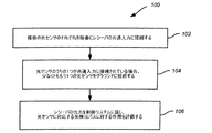
図1は、複数の光センサを動作させる方法100の一例を示している。方法100では、各光センサを順番にレシーバの共通入力に接続する102。光センサのうちの或る1つを前記共通入力に電気的に接続するときに、前記光センサのうちの少なくとももう1つをグラウンドに短絡させる104。
FIG. 1 shows an example of a
方法100の一実施形態では、或る光センサを共通入力に接続するときに、残りの他の光センサを全てグラウンドに短絡させる。他の実施形態では、或る光センサの直ぐ隣りにある光センサを少なくともグラウンドに短絡させる。
In one embodiment of the
前記光センサがそれぞれ、光検出パス(例えば光タッチパッドの光検出パス)に対応する場合、方法100は、レシーバの出力を制御システムに渡し、光検出パスに対する作用を評価するステップを更に含む。
If each of the light sensors corresponds to a light detection path (eg, a light detection path of an optical touchpad), the
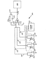
図2は、方法100を実施することが可能な装置200の一例を示している。装置200は、複数の光センサ202、204、206(例えば、(図示のような)PNダイオード等のフォトダイオード)、及び、共通入力210を有するレシーバ208を含む。例えば、図中、レシーバ208は、基準電圧(Vref)を印加するためのもう1つの入力212と、フィードバックパス214とを有する。他の例において、フィードバックパス214は、レシーバの出力216と共通入力210の間に接続され、コンデンサ220に対して並列に接続された抵抗器218を有する場合がある。
FIG. 2 shows an example of an
第1の複数のスイッチ222、224、226はそれぞれ、光センサ202、204、206のうちの1つをレシーバ208の共通入力210に電気的に接続する。第2の複数のスイッチ228、230、232のそれぞれは、光センサ202、204、206のうちの1つをグラウンドに短絡させる。スイッチ222〜232は、様々な形で実施することが可能であるが、一実施形態では、金属酸化膜半導体FET(MOSFET)スイッチのような、電界効果トランジスタ(FET)スイッチの形で実施される。
Each of the first plurality of
一実施形態において、前記複数の第1のスイッチ及び前記複数の第2のスイッチは、走査制御システム234によって作動(例えば、開閉)される。例えば、走査制御システム234は、第1の複数のスイッチ222〜226(すなわち、「直列スイッチ」)のそれぞれを順番に閉じると同時に、残りのスイッチを開くようにプログラムされ、それによって、光センサを一度に1つだけ共通入力210に接続することができる。このようにすると、各光センサ202〜206の状態をレシーバ208によって順番に読み出し、論理回路236に出力することができる。一実施形態において、論理回路236は、レシーバ208から出力されたセンサ状態を記憶するためのラッチ又はレジスタを含む。
In one embodiment, the plurality of first switches and the plurality of second switches are actuated (eg, opened and closed) by a
理論上は、光センサ202〜206を共通入力210に順番に接続すれば、レシーバ208は、一度に1つの光センサの状態しか読み出さないはずである。しかしながら、(1)光センサ202〜206相互間の距離や、(2)光センサ202〜206のうちの幾つかに同時に光が当たるか否かに応じて、光センサ202〜206間、及び、それに関連する信号パス間には、漏話が発生する可能性がある。つまり、光センサをレシーバ208に接続しなくても、光センサに光を当てると、その光センサによって、1以上の他の光センサに電流が誘導されることがある。従って、例えばスイッチ222が閉じていて、光センサ202がレシーバ208に接続され、他には閉じているスイッチ224〜232が何もない場合でも、光が逸れて光センサ204に当たったり、光センサ204に意図的に光を当てたりすると、その変化は、実際には光が当たっていなくても、光センサ202に光が当たっているものとして解釈されることがある。
Theoretically, if the photosensors 202-206 are connected in sequence to the
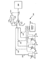
光センサ202〜206間に生じる漏話の可能性を低減するために、走査制御システム234は、(A)レシーバ208に接続された或る光センサに接続されている短絡スイッチを開き、(B)少なくとももう1つの短絡スイッチを閉じることによって、第2の複数のスイッチ228〜232(すなわち、「短絡スイッチ」)を作動させるようにプログラムされる。例えば、図3に示す装置200の状態を見て欲しい。この装置では、直列スイッチ222を閉じると同時にスイッチ224及び226を開き、短絡スイッチ228を開くと同時にスイッチ230及び232を閉じている。
To reduce the possibility of crosstalk occurring between the photosensors 202-206, the
一実施形態において、走査制御システム234は、「アクティブ」な光センサ(すなわち、レシーバ208によって読み出し中の光センサ)に接続された短絡スイッチを除き、他の全ての短絡スイッチを閉じる。他の実施形態では、短絡スイッチのうち、「アクティブ」な光センサの直ぐ隣りの光センサに接続された短絡スイッチだけを閉じる(なぜなら、直ぐ隣りにない光センサが光センサ間の漏話の原因となる可能性は低いからである)。
In one embodiment, the
図3に示す装置200の状態の後、制御システム234は、スイッチ222〜232を図4に示す状態に再構成するであろう。以下同様である。
After the state of the
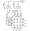
図5に示すように、装置200一つの応用形態は、光入力の検出である。このような実施形態では、装置200の光センサ202〜206は、光検出領域500(例えば、タッチパッド)の片側に配置され、複数の光源502、504、506(例えば、発光ダイオード(LED))が、光検出領域500の、光センサ202〜206とは反対側の面に配置される。このようにすると、光検出領域500全体にわたって、各光源502〜506により、対応する光センサ202〜206を照らすことができる。
As shown in FIG. 5, one application of the
一実施形態において、光源502〜506は、実質的に平行な光ビームを発する。他の実施形態では、光源502〜506は、走査制御システム234によって順番に駆動され、各光源502〜506は、その光源に対応する光センサ202〜206がレシーバ208に接続されるのと同時に駆動される。
In one embodiment, the light sources 502-506 emit substantially parallel light beams. In other embodiments, the light sources 502-506 are driven in turn by the
光検出領域500の残りの縁部に光センサ508〜512及び光源514〜518を更に配置し、それらの光センサ508〜512をレシーバ208又は他のレシーバ520接続してもよい(図示のように)。レシーバ208及び520の出力はいずれも、論理回路236に接続され、論理回路236は光検出領域500に対する作用を評価することができる(例えば、スタイラスや指が接触した座標を検出することにより)。
Photosensors 508-512 and light sources 514-518 may be further arranged at the remaining edge of the
本発明の種々の例示的実施形態を以下に列挙する。
1.複数の光センサを作動させる方法であって、
前記光センサのそれぞれを順番にレシーバの共通入力に接続し、
前記光センサのうちの或る1つを前記共通入力に電気的に接続するときに、前記光センサのうちの少なくとももう1つをグラウンドに短絡させることからなる方法。
2.前記光センサのうちの或る1つを前記共通入力に電気的に接続するときに、少なくともその光センサの直ぐ隣りの光センサをグラウンドに短絡させることを含む、1に記載の方法。
3.前記光センサのうちの或る1つを前記共通入力に接続するときに、他の残りの光センサを全てグラウンドに短絡させることを含む、1に記載の方法。
4.前記光センサのそれぞれが光検出パスに対応し、前記方法は、前記レシーバの出力を制御システムに渡し、前記光検出パスに対する作用を評価することを含む、1に記載の方法。
5.複数の光センサと、
共通入力を有するレシーバと、
各スイッチが、前記光センサのうちの1つを前記レシーバの共通入力に電気的に接続するように構成された、第1の複数のスイッチと、
各スイッチが、前記光センサのうちの1つをグラウンドに短絡させるように構成された、第2の複数のスイッチと
からなる装置。
6.(1)前記第1の複数のスイッチのそれぞれを順番に閉じると同時に前記第1の複数のスイッチの残りのスイッチを開き、(2)或る光センサに接続された前記第1の複数のスイッチのうちの1つを閉じるときに、(A)その光センサに接続された前記第2のスイッチのうちの1つを開くとともに、(B)前記第2のスイッチのうちの少なくとももう1つのスイッチを閉じるようにプログラムされた、走査制御システムを更に含む、5に記載の装置。
7.前記走査制御システムは、或る光センサに接続された前記第2の複数のスイッチのうちの1つを開くときに、前記第2の複数のスイッチのうちの残りのスイッチを全て閉じるように構成される、6に記載の装置。
8.前記走査制御システムは、或る光センサに接続された前記第2の複数のスイッチのうちの1つを開くときに、前記第2の複数のスイッチのうちのその光センサの直ぐ隣りの光センサに接続されたものを少なくとも閉じるように構成される、6に記載の装置。
9.タッチパッドと、
複数の発光ダイオード(LED)と
を更に含み、前記複数の光センサはフォトダイオードであり、
前記タッチパッド全体にわたって、各LEDが、対応する光センサを照らすように構成される、6に記載の装置。
10.光検出領域と、
複数の光源と
を更に含み、前記光検出領域全体にわたって、各光源が、対応する光センサを照らすように構成される、5に記載の装置。
11.前記光検出領域はタッチパッドからなる、10に記載の装置。
12.前記レシーバに接続され、前記光検出領域に対する作用を評価するように構成された論理回路を更に含む、10に記載の装置。
13.前記第1の複数のスイッチ及び前記第2の複数のスイッチは、電界効果トランジスタスイッチからなる、5に記載の装置。
14.前記第1の複数のスイッチ及び前記第2の複数のスイッチは、金属酸化膜半導体電界効果トランジスタ(MOSFET)スイッチからなる、5に記載の装置。
15.前記複数の光センサはフォトダイオードである、5に記載の装置。
16.前記複数の光源は発光ダイオード(LED)である、5に記載の装置。
Various exemplary embodiments of the invention are listed below.
1. A method of operating a plurality of light sensors,
Connect each of the light sensors in turn to a common input of the receiver;
A method comprising shorting at least one of the photosensors to ground when electrically connecting one of the photosensors to the common input.
2. 2. The method of 1, comprising electrically shorting at least one photosensor immediately adjacent to the photosensor to ground when electrically connecting one of the photosensors to the common input.
3. 2. The method of 1, comprising: shorting all other remaining photosensors to ground when connecting one of the photosensors to the common input.
4). The method of
5. A plurality of light sensors;
A receiver having a common input;
A first plurality of switches, each switch configured to electrically connect one of the photosensors to a common input of the receiver;
A device comprising: a second plurality of switches, each switch configured to short one of the photosensors to ground.
6). (1) Close each of the first plurality of switches in turn and simultaneously open the remaining switches of the first plurality of switches, and (2) the first plurality of switches connected to a certain optical sensor. When closing one of (A) opening one of the second switches connected to the photosensor, and (B) at least one other switch of the second switch. 6. The apparatus of 5, further comprising a scanning control system programmed to close the.
7). The scanning control system is configured to close all remaining switches of the second plurality of switches when opening one of the second plurality of switches connected to an optical sensor. The apparatus according to 6, wherein:
8). When the scanning control system opens one of the second plurality of switches connected to an optical sensor, the optical sensor immediately adjacent to the optical sensor of the second plurality of
9. Touchpad,
A plurality of light emitting diodes (LEDs); and the plurality of light sensors are photodiodes;
The apparatus of claim 6, wherein each LED is configured to illuminate a corresponding light sensor across the touchpad.
10. A light detection region;
6. The apparatus of 5, further comprising: a plurality of light sources, wherein each light source is configured to illuminate a corresponding light sensor throughout the light detection region.
11. 11. The apparatus according to 10, wherein the light detection area is a touch pad.
12 The apparatus of 10, further comprising a logic circuit connected to the receiver and configured to evaluate an effect on the light detection region.
13. 6. The apparatus according to 5, wherein the first plurality of switches and the second plurality of switches comprise field effect transistor switches.
14 6. The device according to 5, wherein the first plurality of switches and the second plurality of switches comprise metal oxide semiconductor field effect transistor (MOSFET) switches.
15. 6. The apparatus according to 5, wherein the plurality of optical sensors are photodiodes.
16. 6. The apparatus according to 5, wherein the plurality of light sources are light emitting diodes (LEDs).
Claims (10)
前記光センサ(202,204,206)のそれぞれを順番にレシーバ(208)の共通入力(210)に接続する(102)し、
前記光センサ(202,204,206)のうちの或る1つを前記共通入力(210)に電気的に接続するときに、前記光センサ(202,204,206)のうちの少なくとも1つをグラウンドに短絡させることからなる方法(100)。 A method (100) for operating a plurality of optical sensors (202, 204, 206), comprising:
Each of the light sensors (202, 204, 206) is connected (102) in turn to a common input (210) of a receiver (208),
A method comprising shorting at least one of the light sensors (202, 204, 206) to ground when electrically connecting one of the light sensors (202, 204, 206) to the common input (210) (100).
共通入力(210)を有するレシーバ(208)と、
各スイッチが、前記光センサ(202,204,206)のうちの1つを前記レシーバ(208)の共通入力(210)に電気的に接続するように構成された、第1の複数のスイッチ(222,224,226)と、
各スイッチが、前記光センサ(202,204,206)のうちの1つをグラウンドに短絡させるように構成された、第2の複数のスイッチ(228,230,232)と
からなる装置(200)。 A plurality of light sensors (202, 204, 206);
A receiver (208) having a common input (210);
A first plurality of switches (222, 224, 226), each switch configured to electrically connect one of the light sensors (202, 204, 206) to a common input (210) of the receiver (208);
A device (200) comprising a second plurality of switches (228, 230, 232), each switch configured to short one of the photosensors (202, 204, 206) to ground.
複数の発光ダイオード(LED502,504,506)と
を更に含み、前記複数の光センサ(202,204,206)はフォトダイオードであり、
前記タッチパッド(500)全体にわたって、各LED(502,504,506)が、対応する光センサ(202,204,206)を照らすように構成される、請求項5に記載の装置(200)。 Touchpad (500),
A plurality of light emitting diodes (LED502, 504, 506), and the plurality of light sensors (202, 204, 206) are photodiodes;
The apparatus (200) of claim 5, wherein each LED (502, 504, 506) is configured to illuminate a corresponding light sensor (202, 204, 206) throughout the touchpad (500).
複数の光源(502,504,506)と
を更に含み、前記光検出領域(500)全体にわたって、各光源(502,504,506)が、対応する光センサ(202,204,206)を照らすように構成される、請求項4に記載の装置(200)。 A light detection area (500);
5. The apparatus of claim 4, further comprising: a plurality of light sources (502, 504, 506), wherein each light source (502, 504, 506) is configured to illuminate a corresponding light sensor (202, 204, 206) throughout the light detection region (500). (200).
The apparatus (200) of claim 4, wherein the first plurality of switches and the second plurality of switches (222, 224, 226, 228, 230, 232) comprise field effect transistor switches.
Applications Claiming Priority (1)
| Application Number | Priority Date | Filing Date | Title |
|---|---|---|---|
| US11/141,919 US20060274056A1 (en) | 2005-06-01 | 2005-06-01 | Methods and apparatus for operating optical sensors |
Publications (1)
| Publication Number | Publication Date |
|---|---|
| JP2006337366A true JP2006337366A (en) | 2006-12-14 |
Family
ID=36694709
Family Applications (1)
| Application Number | Title | Priority Date | Filing Date |
|---|---|---|---|
| JP2006151152A Pending JP2006337366A (en) | 2005-06-01 | 2006-05-31 | Method and device for operating optical sensor |
Country Status (4)
| Country | Link |
|---|---|
| US (1) | US20060274056A1 (en) |
| JP (1) | JP2006337366A (en) |
| CN (1) | CN1936810B (en) |
| GB (1) | GB2426814B (en) |
Cited By (1)
| Publication number | Priority date | Publication date | Assignee | Title |
|---|---|---|---|---|
| JP2011524515A (en) * | 2008-05-09 | 2011-09-01 | オムロン サイエンティフィック テクノロジーズ, インコーポレイテッド | Method and apparatus for zone selection in an area monitoring device |
Families Citing this family (6)
| Publication number | Priority date | Publication date | Assignee | Title |
|---|---|---|---|---|
| TWI291237B (en) * | 2005-10-07 | 2007-12-11 | Integrated Digital Technologie | Photo detector array |
| US9064772B2 (en) * | 2005-10-07 | 2015-06-23 | Integrated Digital Technologies, Inc. | Touch screen system having dual touch sensing function |
| US8344313B2 (en) * | 2005-10-07 | 2013-01-01 | Integrated Digital Technologies, Inc. | Optical input type touch system and feedback control method thereof |
| KR101003170B1 (en) * | 2006-09-25 | 2010-12-22 | 인테그레이티드 디지털 테크놀로지스, 인코포레이티드 | Photo Detector Array |
| EP3282234A1 (en) * | 2016-08-09 | 2018-02-14 | ams International AG | Optical sensor arrangement and method for optical sensing |
| US20220382410A1 (en) * | 2021-05-28 | 2022-12-01 | Qualcomm Incorporated | Verification of a user input of a user interface |
Family Cites Families (10)
| Publication number | Priority date | Publication date | Assignee | Title |
|---|---|---|---|---|
| US4205304A (en) * | 1977-09-22 | 1980-05-27 | General Electric Company | Two dimensional light beam selection system |
| JPS61167824A (en) * | 1985-01-18 | 1986-07-29 | Nippon Soken Inc | Photoelectric converting circuit |
| JPS6365325A (en) * | 1986-09-05 | 1988-03-23 | Sharp Corp | Light quantity detecting circuit |
| JPH05288604A (en) * | 1992-04-10 | 1993-11-02 | Olympus Optical Co Ltd | Photometer |
| US5352887A (en) * | 1992-08-28 | 1994-10-04 | Motorola, Inc. | Circuit for detecting a droplet in motion and method therefor |
| US5321252A (en) * | 1993-05-03 | 1994-06-14 | Pitney Bowes Inc. | Improved driver circuitry for multiple sensors |
| JP3527911B2 (en) * | 1997-05-20 | 2004-05-17 | 富士電機デバイステクノロジー株式会社 | Optical sensor monitor circuit |
| JP2001133325A (en) * | 1999-11-08 | 2001-05-18 | Seiko Precision Inc | Photometric device |
| US6781570B1 (en) * | 2000-11-09 | 2004-08-24 | Logitech Europe S.A. | Wireless optical input device |
| JP2005283279A (en) * | 2004-03-29 | 2005-10-13 | Victor Co Of Japan Ltd | Photoelectric conversion circuit |
-
2005
- 2005-06-01 US US11/141,919 patent/US20060274056A1/en not_active Abandoned
-
2006
- 2006-05-31 GB GB0610772A patent/GB2426814B/en not_active Expired - Fee Related
- 2006-05-31 JP JP2006151152A patent/JP2006337366A/en active Pending
- 2006-06-01 CN CN200610138872XA patent/CN1936810B/en not_active Expired - Fee Related
Cited By (1)
| Publication number | Priority date | Publication date | Assignee | Title |
|---|---|---|---|---|
| JP2011524515A (en) * | 2008-05-09 | 2011-09-01 | オムロン サイエンティフィック テクノロジーズ, インコーポレイテッド | Method and apparatus for zone selection in an area monitoring device |
Also Published As
| Publication number | Publication date |
|---|---|
| CN1936810A (en) | 2007-03-28 |
| US20060274056A1 (en) | 2006-12-07 |
| GB2426814A (en) | 2006-12-06 |
| GB2426814B (en) | 2010-03-10 |
| GB0610772D0 (en) | 2006-07-12 |
| CN1936810B (en) | 2010-06-16 |
Similar Documents
| Publication | Publication Date | Title |
|---|---|---|
| JP2006337366A (en) | Method and device for operating optical sensor | |
| CN100593857C (en) | Photoelectric transducer and display panel having the same | |
| US8310381B2 (en) | Capacitive key touch sensing using analog inputs and digital outputs | |
| US8427450B2 (en) | Capacitive touch sensing and light emitting diode drive matrix | |
| US10671218B2 (en) | Floating touch control panel, touch control method of the same, and display device | |
| EP3076383B1 (en) | Touch control circuit and drive method therefor, array substrate and touch control display device | |
| JP4725482B2 (en) | Photosensor, photosensor target detection method and display device | |
| TWI395170B (en) | Liquid-crystal display apparatus | |
| US20120056853A1 (en) | Optical touch device and method therefor | |
| US11893188B2 (en) | Optical touch sensor devices and systems | |
| US11625128B2 (en) | Optical touch sensor systems and optical detectors with noise mitigation | |
| KR20090010059A (en) | Detection circuit for detecting movements of a movable object | |
| US9182834B2 (en) | Mouse device | |
| TWI764161B (en) | light detection device | |
| TW201512950A (en) | OLED touch device | |
| WO2021095788A1 (en) | Detection device | |
| JP2013156085A (en) | Photodetector, object detection sensor, and electronic apparatus | |
| US10678361B2 (en) | Touch circuit, touch array circuit and method for driving the same, and display panel | |
| US20120169666A1 (en) | Optical touch-sensing liquid crystal panel, optical touch-sensing panel and method of determining touch position | |
| US10884559B2 (en) | Touch panel, touch method of the same, and touch apparatus | |
| KR101275161B1 (en) | Capacitive touch sensing device | |
| CN112599060A (en) | VT test circuit, system, method, display panel and display device | |
| KR101275158B1 (en) | Capacitive touch sensing device | |
| EP3422158B1 (en) | Touch sensitive user interface and method for operating a touch sensitive user interface | |
| US20130100078A1 (en) | Photo-sensor type input apparatus for identifying different types of input events simultaneously, and related display apparatus thereof |