EP2912726B1 - Leadframe module for an electrical connector - Google Patents
Leadframe module for an electrical connector Download PDFInfo
- Publication number
- EP2912726B1 EP2912726B1 EP13786107.6A EP13786107A EP2912726B1 EP 2912726 B1 EP2912726 B1 EP 2912726B1 EP 13786107 A EP13786107 A EP 13786107A EP 2912726 B1 EP2912726 B1 EP 2912726B1
- Authority
- EP
- European Patent Office
- Prior art keywords
- contacts
- leadframe
- transmission lines
- dielectric
- module
- Prior art date
- Legal status (The legal status is an assumption and is not a legal conclusion. Google has not performed a legal analysis and makes no representation as to the accuracy of the status listed.)
- Active
Links
Images


Classifications
-
- H—ELECTRICITY
- H01—ELECTRIC ELEMENTS
- H01R—ELECTRICALLY-CONDUCTIVE CONNECTIONS; STRUCTURAL ASSOCIATIONS OF A PLURALITY OF MUTUALLY-INSULATED ELECTRICAL CONNECTING ELEMENTS; COUPLING DEVICES; CURRENT COLLECTORS
- H01R12/00—Structural associations of a plurality of mutually-insulated electrical connecting elements, specially adapted for printed circuits, e.g. printed circuit boards [PCB], flat or ribbon cables, or like generally planar structures, e.g. terminal strips, terminal blocks; Coupling devices specially adapted for printed circuits, flat or ribbon cables, or like generally planar structures; Terminals specially adapted for contact with, or insertion into, printed circuits, flat or ribbon cables, or like generally planar structures
- H01R12/70—Coupling devices
- H01R12/71—Coupling devices for rigid printing circuits or like structures
- H01R12/72—Coupling devices for rigid printing circuits or like structures coupling with the edge of the rigid printed circuits or like structures
- H01R12/722—Coupling devices for rigid printing circuits or like structures coupling with the edge of the rigid printed circuits or like structures coupling devices mounted on the edge of the printed circuits
- H01R12/727—Coupling devices presenting arrays of contacts
-
- H—ELECTRICITY
- H01—ELECTRIC ELEMENTS
- H01R—ELECTRICALLY-CONDUCTIVE CONNECTIONS; STRUCTURAL ASSOCIATIONS OF A PLURALITY OF MUTUALLY-INSULATED ELECTRICAL CONNECTING ELEMENTS; COUPLING DEVICES; CURRENT COLLECTORS
- H01R12/00—Structural associations of a plurality of mutually-insulated electrical connecting elements, specially adapted for printed circuits, e.g. printed circuit boards [PCB], flat or ribbon cables, or like generally planar structures, e.g. terminal strips, terminal blocks; Coupling devices specially adapted for printed circuits, flat or ribbon cables, or like generally planar structures; Terminals specially adapted for contact with, or insertion into, printed circuits, flat or ribbon cables, or like generally planar structures
- H01R12/70—Coupling devices
- H01R12/71—Coupling devices for rigid printing circuits or like structures
- H01R12/72—Coupling devices for rigid printing circuits or like structures coupling with the edge of the rigid printed circuits or like structures
-
- H—ELECTRICITY
- H01—ELECTRIC ELEMENTS
- H01R—ELECTRICALLY-CONDUCTIVE CONNECTIONS; STRUCTURAL ASSOCIATIONS OF A PLURALITY OF MUTUALLY-INSULATED ELECTRICAL CONNECTING ELEMENTS; COUPLING DEVICES; CURRENT COLLECTORS
- H01R13/00—Details of coupling devices of the kinds covered by groups H01R12/70 or H01R24/00 - H01R33/00
- H01R13/02—Contact members
- H01R13/03—Contact members characterised by the material, e.g. plating, or coating materials
- H01R13/035—Plated dielectric material
-
- H—ELECTRICITY
- H01—ELECTRIC ELEMENTS
- H01R—ELECTRICALLY-CONDUCTIVE CONNECTIONS; STRUCTURAL ASSOCIATIONS OF A PLURALITY OF MUTUALLY-INSULATED ELECTRICAL CONNECTING ELEMENTS; COUPLING DEVICES; CURRENT COLLECTORS
- H01R13/00—Details of coupling devices of the kinds covered by groups H01R12/70 or H01R24/00 - H01R33/00
- H01R13/648—Protective earth or shield arrangements on coupling devices, e.g. anti-static shielding
- H01R13/658—High frequency shielding arrangements, e.g. against EMI [Electro-Magnetic Interference] or EMP [Electro-Magnetic Pulse]
- H01R13/6581—Shield structure
- H01R13/6585—Shielding material individually surrounding or interposed between mutually spaced contacts
-
- H—ELECTRICITY
- H01—ELECTRIC ELEMENTS
- H01R—ELECTRICALLY-CONDUCTIVE CONNECTIONS; STRUCTURAL ASSOCIATIONS OF A PLURALITY OF MUTUALLY-INSULATED ELECTRICAL CONNECTING ELEMENTS; COUPLING DEVICES; CURRENT COLLECTORS
- H01R12/00—Structural associations of a plurality of mutually-insulated electrical connecting elements, specially adapted for printed circuits, e.g. printed circuit boards [PCB], flat or ribbon cables, or like generally planar structures, e.g. terminal strips, terminal blocks; Coupling devices specially adapted for printed circuits, flat or ribbon cables, or like generally planar structures; Terminals specially adapted for contact with, or insertion into, printed circuits, flat or ribbon cables, or like generally planar structures
- H01R12/70—Coupling devices
- H01R12/71—Coupling devices for rigid printing circuits or like structures
- H01R12/72—Coupling devices for rigid printing circuits or like structures coupling with the edge of the rigid printed circuits or like structures
- H01R12/722—Coupling devices for rigid printing circuits or like structures coupling with the edge of the rigid printed circuits or like structures coupling devices mounted on the edge of the printed circuits
- H01R12/724—Coupling devices for rigid printing circuits or like structures coupling with the edge of the rigid printed circuits or like structures coupling devices mounted on the edge of the printed circuits containing contact members forming a right angle
-
- H—ELECTRICITY
- H01—ELECTRIC ELEMENTS
- H01R—ELECTRICALLY-CONDUCTIVE CONNECTIONS; STRUCTURAL ASSOCIATIONS OF A PLURALITY OF MUTUALLY-INSULATED ELECTRICAL CONNECTING ELEMENTS; COUPLING DEVICES; CURRENT COLLECTORS
- H01R13/00—Details of coupling devices of the kinds covered by groups H01R12/70 or H01R24/00 - H01R33/00
- H01R13/648—Protective earth or shield arrangements on coupling devices, e.g. anti-static shielding
- H01R13/658—High frequency shielding arrangements, e.g. against EMI [Electro-Magnetic Interference] or EMP [Electro-Magnetic Pulse]
- H01R13/6581—Shield structure
- H01R13/6585—Shielding material individually surrounding or interposed between mutually spaced contacts
- H01R13/6586—Shielding material individually surrounding or interposed between mutually spaced contacts for separating multiple connector modules
- H01R13/6587—Shielding material individually surrounding or interposed between mutually spaced contacts for separating multiple connector modules for mounting on PCBs
Definitions
- the subject matter herein relates generally to leadframe modules for electrical connectors.
- the electrical connectors typically include chicklets or contact modules that are loaded into a housing for mating with a corresponding mating connector.
- the contact modules typically include overmolded leadframes manufactured from leadframes that are overmolded with dielectric material.
- shielding is needed for the individual contacts of the contact modules.
- the overmolded dielectric body of the contact module needs to be redesigned. Such redesign typically requires expensive tooling and dies, making the overall manufacturing costs very high.
- WO 01/57964 discloses an electrical connector manufactured with wafer assemblies.
- Each wafer assembly has wafers forming pairs of signal conductors and shield strips, each pair of signal conductors having a shield strip running parallel it.
- a signal contact blank having the signal conductors is formed by stamping from a sheet of metal.
- US 2010/0048058 discloses an electrical connector including a housing and lead frame held by the housing.
- the lead frame includes a terminal extending between mating and mounting end portions.
- the terminal is surrounded by a dielectric core, and the dielectric core is surrounded by an electrically conductive shell.
- the leadframe module includes a leadframe having contacts initially held together as part of the leadframe.
- the contacts have mating ends configured to be mated to corresponding mating contacts.
- the contacts having mounting ends configured to be terminated to corresponding conductors.
- Each contact is coated with a corresponding dielectric shell.
- a conductive outer shield is applied to the corresponding dielectric shell to individually shield the contact.
- Each of the contacts, dielectric shells and outer shields define corresponding shielded transmission lines of the leadframe module.
- a ground plate is coupled to each of the transmission lines and electrically connected to the outer shields of the transmission lines to electrically common each of the outer shields.
- FIG. 1 is a perspective view of an exemplary embodiment of an electrical connector system 100 illustrating a receptacle connector 102 and a header connector 104 that may be directly mated together.
- the electrical connector system 100 may be a high speed connector system passing high speed signals.
- the electrical connector system 100 may include a plurality of transmission lines defined between circuit boards 106, 108.
- the system 100 may form part of a network or server system.
- the electrical connector system 100 may form part of a backplane system with the header connector 104 defining a backplane side of the system 100 and the receptacle connector 102 defining a daughtercard side of the system 100. While the subject matter is described herein with reference to transmission lines for use in a high speed connector system, the subject matter is not limited to such application, and is but one example of an application that could use the transmission line structure described herein.
- the receptacle connector 102 includes a housing 120 that holds a plurality of leadframe modules 122. Any number of leadframe modules 122 may be provided to increase the density of the receptacle connector 102.
- the leadframe modules 122 each include a plurality of contacts 124 (shown in Figure 2 ) that are received in the housing 120 for mating with the header connector 104. In an exemplary embodiment, each contact 124 forms part of a shielded transmission line configured to convey data signals.
- the receptacle connector 102 includes a mating end 128 and a mounting end 130.
- the contacts 124 are received in the housing 120 and held therein at the mating end 128 for mating to the header connector 104.
- the contacts 124 are arranged in a matrix of rows and columns. Any number of contacts 124 may be provided in the rows and columns.
- the contacts 124 also extend to the mounting end 130 for mounting to the circuit board 106.
- the mounting end 130 may be substantially perpendicular to the mating end 128, defining a right angle receptacle connector.
- the mating end 128 and mounting end 130 may be parallel to each other, defining a mezzanine connector.
- the housing 120 includes a plurality of signal contact openings 132 and a plurality of ground contact openings 134 at the mating end 128.
- the contacts 124 are received in corresponding signal contact openings 132.
- a single contact 124 is received in each signal contact opening 132.
- the signal contact openings 132 may also receive corresponding header signal contacts 144 therein when the receptacle and header connectors 102, 104 are mated.
- the ground contact openings 134 receive header shields 146 therein when the receptacle and header connectors 102, 104 are mated.
- the ground contact openings 134 receive grounding beams 228 (shown in Figure 2 ) of the leadframe modules 122 that mate with the header shields 146 to electrically common the receptacle and header connectors 102, 104.
- the housing 120 is manufactured from a dielectric material, such as a plastic material.
- the housing 120 provides support for the leadframe modules 122.
- the housing 120 holds the leadframe modules 122 along parallel planes.
- the leadframe modules 122 may be loaded into the rear of the housing 120 and extend rearward therefrom with portions of the leadframe modules 122 exposed.
- the housing 120 may cover the entire leadframe modules 122, such as to protect the leadframe modules 122 from damage.
- the leadframe modules 122 may be loaded into the housing 120 through a top or a bottom of the housing 120 rather than through the rear of the housing 120.
- the housing 120 may include channels separated by walls that support and position the leadframe modules 122 within the housing 120.
- the header connector 104 includes a header housing 138 having walls 140 defining a chamber 142.
- the header connector 104 has a mating end 150 and a mounting end 152 that is mounted to the circuit board 108.
- the mounting end 152 may be substantially parallel to the mating end 150.
- the receptacle connector 102 is received in the chamber 142 through the mating end 150.
- the housing 120 engages the walls 140 to hold the receptacle connector 102 in the chamber 142.
- the header signal contacts 144 and the header shields 146 extend from a base wall 148 into the chamber 142.
- the header signal contacts 144 and the header shields 146 extend through the base wall 148 and are mounted to the circuit board 108.
- the header signal contacts 144 are arranged as differential pairs.
- the header shields 146 are positioned between the differential pairs to provide electrical shielding between adjacent differential pairs.
- the header shields 146 are C-shaped and provide shielding on three sides of the pair of header signal contacts 144.
- the header signal contacts may be arranged as single contacts with shielding at appropriate locations.
- the header shields 146 may have other shapes in alternative embodiments.
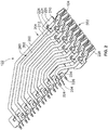
- FIG 2 is a side perspective view of the leadframe module 122 formed in accordance with an exemplary embodiment.
- Figure 3 is another side view of the leadframe module 122.
- the leadframe module 122 includes a plurality of transmission lines 200 configured to convey data signals.
- the transmission lines 200 may convey high speed data signals.
- the transmission lines 200 are separated by air gaps 260 and do not include overmolded dielectric bodies holding all of the contacts 124 together as part of a common module, as is common of conventional contact modules.
- the transmission lines 200 are individually electrically shielded.
- Each transmission line 200 includes a corresponding contact 124.
- the contact 124 extends between a mating end 202 and a mounting end 204.
- the mating ends 202 of the contacts 124 are configured to be mated to corresponding mating contacts, such as the header signal contacts 144 (shown in Figure 1 ).
- the mating ends 202 each include a pair of opposed spring beams configured to receive the header signal contact 144 there between.
- Other types of mating interfaces may be provided that the mating ends 202 in alternative embodiments.
- the mounting ends 204 of the contacts 124 are configured to be terminated to corresponding conductors.
- the mounting ends 204 may be terminated to traces, plated vias, or pads on the circuit board 106 (shown in Figure 1 ) defining electrical conductors of the circuit board 106.
- the mounting ends 204 may be terminated to other types of conductors in alternative embodiments.
- the mounting ends 204 may be terminated to corresponding wires or cables rather than the circuit board 106.
- the mounting ends 204 of the contacts 124 are solder pins configured to be inserted into plated vias of the circuit board 106 and soldered therein to make an electrical connection to the circuit board 106.
- the mounting ends 204 of the contacts 124 may be compliant pins or other types of contacts.
- the contacts 124 include transition portions 206 extending between the mating and mounting ends 202, 204.
- the contacts 124 are right angle contacts with the mating ends 202 being generally perpendicular to the mounting ends 204.
- Each of the contacts 124 have a different length than any adjacent contact 124.
- the transition portions 206 each have different length.
- the transmission lines 200 include dielectric shells 210 coating corresponding contacts 124.
- the transmission lines 200 include outer shields 212 applied to corresponding dielectric shells 210.
- the outer shields 212 provide electrical shielding for corresponding contacts 124.
- the dielectric shells 210 electrically separate the contacts 124 from the corresponding outer shields 212.
- the outer shields 212 individually shield each of the contacts 124 along a majority of the length of the contacts 124.
- the outer shields 212 extend generally along the entire length of the transmission portions 206 of the contacts 124.
- the transmission portions 206 are entirely peripherally surrounded by corresponding dielectric shells 210.
- the dielectric shells 210 are entirely peripherally surrounded by corresponding outer shields 212.
- the spacing between the outer shields 212 and the contacts 124 may be controlled to control an impedance of the transmission lines 200.
- the thickness of the dielectric shells 210 may be controlled to define a separation distance between the outer shields 212 and the contacts 124. Tight control of the positioning of the outer shields 212 with respect to the contacts 124 may achieve a target impedance for the transmission lines 200 to increase performance of the receptacle connector 102.
- the transmission lines 200 are separated by the air gaps 260.
- the leadframe module 122 includes ground plates 220, 222 coupled to each of the transmission lines 200.
- the ground plates 220, 222 are configured to be electrically connected to the outer shields 212 of the transmission lines 200 to electrically common each of the outer shields 212.
- the ground plates 220, 222 provide mechanical support for the transmission lines 200.
- the front ground plate 220 is positioned proximate to the mating ends 202 of the contacts 124 and the bottom ground plate 222 is positioned proximate to the mounting ends 204 of the contacts 124. Any number of ground plates may be used.
- the ground plates 220, 222 may be connected together to control the relative positions of the ground plates 220, 222.
- the ground plates may extend along the entire transition portions 206 rather than be located just at the mating ends 202 and mounting end 204.
- the ground plates 220, 222 are generally planar and extend along one side of the transmission lines 200.
- the ground plates 220, 222 include fingers 224 that engage and hold the transmission lines 200.
- the fingers 224 may be crimped around the transmission lines 200.
- the fingers 224 may be stamped from the ground plates 220, 222 and wrapped around the transmission lines 200.
- the fingers 224 directly engage the outer shields 212 to electrically connect the ground plates 220, 222 to the transmission lines 200.
- the bottom ground plate 222 includes pins 226 extending therefrom.
- the pins 226 are configured to be electrically connected to a ground plane of the circuit board 106 (shown in Figure 1 ).
- the pins 226 are compliant pins, such as eye of the needle contacts, that are configured to be loaded into vias of the circuit board 106.
- the ground plate 220 is directly grounded to the circuit board 106.
- the ground plate 220 provides a grounded electrical path between the outer shields 212 and the circuit board 106.
- the front ground plate 220 includes a plurality of ground beams 228 extended forward therefrom.
- the ground beams 228 are positioned between adjacent contacts 124.
- the ground beams 228 extend along the mating ends 202 of the contacts 124.
- the ground beams 228 are configured to be electrically connected to corresponding header shields 146 (shown in Figure 1 ) when the receptacle connector 102 is mated to the header connector 104 (both shown in Figure 1 ).
- the ground beams 228 may be deflectable such that the ground beams 228 may be biased against the header shields 146 when mated thereto.
- the ground beams 228 create a grounded electrical path between the leadframe module 122 and the header connector 104.
- the grounding beams 228 provide electrical shielding between the mating ends 202 of the contacts 124.
- the ground beam 228 are stamped from the ground plate 222 and bent approximately perpendicularly with respect to the ground plate 222 to position the ground beams 228 in plane with the mating ends 202 of the contacts 124.
- the leadframe module 122 may be manufactured inexpensively and without the need for large tooling costs to design and develop the leadframe module 122.
- conventional chicklets include over molded leadframes that include complicated shielding structures to provide electrical shielding between adjacent leads of the leadframe.
- the leadframe module 122 is manufactured simply by coating the dielectric shells 210 over the contacts 124 and then applying the outer shields 212 to the dielectric shells 210.
- the coating and shield application may be easily applied to the contacts 124 irrespective of the size, shape, spacing or other physical parameters of the contacts 124, whereas expensive tools and dies are needed to redesign the over mold of the leadframe of conventional chicklets when any modifications to the chicklet design are needed.
- FIG 4 illustrates a leadframe 250 formed in accordance with an exemplary embodiment.
- the leadframe 250 may be stamped and formed from a stock metal sheet. After being stamped, the leadframe 250 includes a carrier 252 holding a plurality of the contacts 124. The carrier 252 is later removed when the contacts 124 are singulated from one another.
- the transition portions 206, mating ends 202 and mounting ends 204 are all stamped and formed from the stock piece of metal and initially held together by the carrier 252.
- the leadframe 250 may be processed to form the transmission lines 200 (shown in Figures 2 and 3 ).
- the leadframe 250 may be coated with a dielectric material to form the dielectric shells 210 (shown in Figures 2 and 3 ).
- the dielectric shells 210 may be covered by conductive layers to form the outer shields 212 (shown in Figures 2 and 3 ).
- FIG. 5 is a cross sectional view of the transmission line 200 formed in accordance with an exemplary embodiment.
- the transmission line 200 includes the contact 124, the dielectric shell 210 surrounding the contact 124 and the outer shield 212 surrounding the dielectric shell 210.
- the air gaps 260 are defined between adjacent transmission lines 200.
- Figure 6 illustrates a machine used to manufacture leadframe modules 122 and receptacle connectors 102.
- the leadframe modules 122 are continuously manufactured using a reel system to pull the product through the machine 300.
- the product is initially wound on a reel 302 and is feed through the machine 300 from the reel 302.
- the product may be a metal strip that is fed from the reel 302.
- the machine 300 includes a stamp 304 or press that is used to stamp the leadframe 250 (shown in Figure 4 ) from the metal sheet. During the stamping, portions of the sheet may be removed and recycled leaving the contacts 124 (shown in Figure 4 ) on the carrier 252 (shown in Figure 4 ). The contacts 124 may be formed or bent during the stamping process.
- the machine 300 includes a coating station 306.
- the coating station 306 may be a powder coating station.
- the coating station 306 applies the dielectric shell 210 to the contacts 124.
- the dielectric shell 210 may be spray coated or may be coated using a fluidized bed.
- the leadframe 250 is electrically grounded and electrically charged powder is applied to the leadframe 250.
- portions of the leadframe 250 may be masked or otherwise covered to resist coating in such areas.
- Such selective coating applies the dielectric shells 210 to the transition portions 206 as oppose to the mating ends 202 and mounting ends 204.
- the conductive metal of the contacts 124 remains exposed at the mating end 202 and mounting end 204.
- the thickness of the dielectric shells 210 may be controlled by controlling an amount of time that the product is at the coating station 306, by changing the voltage applied to the leadframe 250, by changing the material of the dielectric shells 210 and the like.
- the dielectric shells 210 may have uniform thicknesses radially surrounding the entire contacts 124.
- the machine 300 may include other types of stations other than the coating station 306 to apply the dielectric material to the leadframe 250.
- the dielectric material may be printed on the contacts 124 by a printing station, the dielectric material may be applied by a chemical vapor deposition process, by a physical vapor deposition process, by a dipping process, by a spraying process or by other processes known in the art to apply dielectric material to a substrate.
- the machine 300 includes a post processing station 308 downstream of coating station 306.
- the post processing station 308 is used to process the leadframe 250 and the dielectric shell 210 to prepare the dielectric shells 210 for applying the outer shields 212 thereto.
- the dielectric shells 210 may be thermally cured in a reflow oven to cure the dielectric material.
- the dielectric shells 210 may be cleaned and or may be selectively removed from the contact 124 at the post processing station 308. Other post processing functions may be performed at the post processing station 308.
- the machine 300 includes an application station 310.
- the outer shields 212 are applied to the dielectric shells 210 at the application station 310.
- the application station 310 may be a printing station, wherein conductive ink is printed directly on the dielectric shells 210.
- the conductive ink may be printed using a pad printer, an ink jet printer or another type of printer.
- the conducive layer defining the outer shields 212 may be applied by other processes such as a spraying process, a plating process, or another type of process known in the art to apply a conductive layer to a substrate.
- the conductive layer may be processed to enhance characteristics of the conductive layer, such as to enhance the conductivity of the conductive layer.
- a conductive ink may initially be applied to the dielectric shells to form a base conductive layer, and the base conductive layer may then be further processed, such as by electro-plating or electro-less plating.
- the application station 310 applies the conductive layers to the dielectric shells 210 such that the conductive layers entirely peripherally surround the dielectric shells 210.
- the contacts 124 have 360° shielding providing by the outer shields 212.
- the machine 300 includes a second post processing station 312 after the application station 310.
- the leadframe 250 may be processed, such as to cure the outer shields 212.
- the carrier 252 may be removed, such as by stamping or cutting the carrier 252 from the contacts 124.
- the ground plates 220 may be coupled to the transmission lines 200.
- the leadframe module 122 may be inserted into the housing 120 to form the receptacle connector 102.
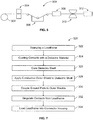
- Figure 7 illustrates a method 320 of manufacturing a leadframe module 122 and a receptacle connector 102.
- the method includes stamping a leadframe from a metal sheet.
- the contacts 124 thereof are initially held together by a carrier 252, which is later removed.
- the method includes coating the contacts 124 with the dielectric material to form the dielectric shells 210.
- the contacts 124 may be selectively plated along certain portions of the contacts 124.
- the transition portions 206 may be coated with the dielectric material.
- the coating may be applied by powder coating the contacts 124.
- the dielectric material may be sprayed onto the contacts 124.
- the dielectric material may be dip coated by submersing the leadframe 250 in a bath or bed of electrically charged, powdered dielectric material. Other types of coating processes may be used in alternative embodiments.
- the dielectric shells 210 may be applied to the contacts 124 by other processes other than coating in alternative embodiments.
- the dielectric shells are cured.
- the leadframe 250 may be passed through a reflow oven to thermally cure the dielectric material to form the dielectric shells 210.
- the method includes applying conductive outer shields 212 to the dielectric shells 210.
- the outer shields 212 may be applied by printing conductive layer onto the dielectric shells 210.
- the conductive layer may be applied by printing conductive ink on the dielectric shell 210.
- a silver ink maybe printed on the dielectric shell 210.
- the conductive ink may be pad printed, ink jet printed, or printed by other processes.
- the outer shields 212 may be applied to the dielectric shells 210 by other processes in alternative embodiments.
- the method includes coupling the ground plates 222, 220 to the outer shields 212.
- the ground plates 220, 222 may be coupled to the outer shields 212 by crimping the fingers 224 to the outer shields 212.
- Other securing means or processes may be used in alternative embodiments, such as soldering the ground plates 220, 222 to the outer shields 212.
- the method includes singulating the contacts 124 from the carrier 252 of the leadframe 250.
- the contacts 124 may be singulated from the carrier 252 by punching, cutting, or otherwise removing the carrier 252 from the leadframe 250. Once the contacts 124 are singulated, the contacts 124 are electrically isolated from each other such that the contacts 124 may convey different signals.
- the carrier 252 is removed after the ground plates 220, 222 are coupled to the outer shields 212.
- the ground plates 220, 222 provide structural support for the transmission lines 200 and allow removal of the carrier 252.
- the method includes loading the leadframe modules 122 into the housing 120 of the receptacle connector 102.
- a plurality of the leadframe modules 122 may be loaded into the housing 120 to form the receptacle connector 102.
- FIG 8 illustrates a leadframe module 402 formed in accordance with an exemplary embodiment.
- the leadframe module 402 is similar to the leadframe module 122 (shown in Figures 2 and 3 ) however the leadframe module 402 includes a single ground plate 404.
- the ground plate 404 is L-shaped and extends along mating and mounting ends of transmission lines 406 of the leadframe module 402.
- the transmission lines 406 may be more rigidly held together by having a single ground plate 404 rather than the front and bottom ground plates 220, 222 (shown in Figures 2 and 3 ).
- FIG 9 illustrates a leadframe module 422 formed in accordance with an exemplary embodiment.
- the leadframe module 422 is similar to the leadframe modules 122 (shown in Figures 2 and 3 ) and 402 (shown in Figure 8 ), however the leadframe module 422 includes a single ground plate 424 having a plurality of spokes 426.
- the ground plate 424 extends along mating and mounting ends of transmission lines 428 of the leadframe module 422 as well as along central portions of the transmission lines 428 to provide additional support for the transmission lines 428.
Landscapes
- Details Of Connecting Devices For Male And Female Coupling (AREA)
Applications Claiming Priority (2)
| Application Number | Priority Date | Filing Date | Title |
|---|---|---|---|
| US13/658,340 US9093800B2 (en) | 2012-10-23 | 2012-10-23 | Leadframe module for an electrical connector |
| PCT/US2013/066264 WO2014066445A1 (en) | 2012-10-23 | 2013-10-23 | Leadframe module for an electrical connector |
Publications (2)
| Publication Number | Publication Date |
|---|---|
| EP2912726A1 EP2912726A1 (en) | 2015-09-02 |
| EP2912726B1 true EP2912726B1 (en) | 2018-01-17 |
Family
ID=49517758
Family Applications (1)
| Application Number | Title | Priority Date | Filing Date |
|---|---|---|---|
| EP13786107.6A Active EP2912726B1 (en) | 2012-10-23 | 2013-10-23 | Leadframe module for an electrical connector |
Country Status (7)
| Country | Link |
|---|---|
| US (1) | US9093800B2 (enExample) |
| EP (1) | EP2912726B1 (enExample) |
| JP (1) | JP2015532523A (enExample) |
| KR (1) | KR101708577B1 (enExample) |
| CN (1) | CN104737374B (enExample) |
| TW (1) | TW201429058A (enExample) |
| WO (1) | WO2014066445A1 (enExample) |
Families Citing this family (19)
| Publication number | Priority date | Publication date | Assignee | Title |
|---|---|---|---|---|
| US9331448B2 (en) * | 2014-03-25 | 2016-05-03 | Tyco Electronics Corporation | Electrical connector having primary and secondary leadframes |
| US9425556B1 (en) * | 2015-07-17 | 2016-08-23 | Tyco Electronics Corporation | Interconnection system and an electrical connector having resonance control |
| KR102106000B1 (ko) * | 2016-06-18 | 2020-05-04 | 몰렉스 엘엘씨 | 선택적으로 차폐되는 커넥터 채널 |
| US9831608B1 (en) * | 2016-10-31 | 2017-11-28 | Te Connectivity Corporation | Electrical connector having ground shield that controls impedance at mating interface |
| US10096924B2 (en) * | 2016-11-21 | 2018-10-09 | Te Connectivity Corporation | Header contact for header connector of a communication system |
| US10186810B2 (en) * | 2017-01-27 | 2019-01-22 | Te Connectivity Corporation | Shielding structure for a contact module |
| US10236645B1 (en) * | 2017-10-26 | 2019-03-19 | All Best Precision Technology Co., Ltd. | Electrical connector |
| US10283914B1 (en) * | 2017-10-27 | 2019-05-07 | Te Connectivity Corporation | Connector assembly having a conductive gasket |
| US10559929B2 (en) * | 2018-01-25 | 2020-02-11 | Te Connectivity Corporation | Electrical connector system having a PCB connector footprint |
| CN108232691B (zh) * | 2018-01-29 | 2023-12-01 | 欧品电子(昆山)有限公司 | 双屏蔽高速对接连接器 |
| USD896763S1 (en) * | 2019-06-05 | 2020-09-22 | Starconn Electronic (Su Zhou) Co., Ltd. | Connector |
| CN110994227B (zh) * | 2019-06-06 | 2021-06-18 | 富鼎精密工业(郑州)有限公司 | 电连接器 |
| CN110994284B (zh) * | 2019-06-06 | 2021-06-18 | 富鼎精密工业(郑州)有限公司 | 电连接器 |
| US11081841B2 (en) | 2019-06-06 | 2021-08-03 | Fu Ding Precision Industrial (Zhengzhou) Co., Ltd. | Electrical connector haiving contact wafer equipped with transverse grounding bar |
| CN114665330B (zh) * | 2020-12-22 | 2023-01-06 | 华为技术有限公司 | 一种连接器、功能板及板级架构 |
| US11955752B2 (en) | 2021-02-02 | 2024-04-09 | Lotes Co., Ltd | Electrical connector |
| US12381361B2 (en) | 2021-05-12 | 2025-08-05 | Lotes Co., Ltd | Electrical connecting assembly |
| CN113937568B (zh) * | 2021-09-08 | 2024-09-20 | 中航光电科技股份有限公司 | 一种信号连接器 |
| CN116191102A (zh) * | 2023-02-23 | 2023-05-30 | 中航光电科技股份有限公司 | 端子模块的端子传输单元及端子模块、连接器 |
Citations (1)
| Publication number | Priority date | Publication date | Assignee | Title |
|---|---|---|---|---|
| US20100048058A1 (en) * | 2008-08-19 | 2010-02-25 | Chad William Morgan | Electrical connector with electrically shielded terminals |
Family Cites Families (45)
| Publication number | Priority date | Publication date | Assignee | Title |
|---|---|---|---|---|
| US4401355A (en) * | 1981-07-01 | 1983-08-30 | Rca Corporation | Filtered connector |
| US4451107A (en) * | 1982-08-23 | 1984-05-29 | Amp Incorporated | High speed modular connector for printed circuit boards |
| DE69018000T2 (de) | 1989-10-10 | 1995-09-28 | Whitaker Corp | Rückwandsteckverbinder mit angepasster Impedanz. |
| US5169343A (en) | 1990-11-29 | 1992-12-08 | E. I. Du Pont De Nemours And Company | Coax connector module |
| JPH0831527A (ja) | 1994-07-04 | 1996-02-02 | Whitaker Corp:The | 基板用コネクタ |
| US5993259A (en) * | 1997-02-07 | 1999-11-30 | Teradyne, Inc. | High speed, high density electrical connector |
| US6231391B1 (en) * | 1999-08-12 | 2001-05-15 | Robinson Nugent, Inc. | Connector apparatus |
| DE19902034A1 (de) * | 1999-01-20 | 2000-07-27 | Continental Teves Ag & Co Ohg | Hydraulikaggregat mit Steckverbindung |
| JP3178455B2 (ja) * | 1999-03-04 | 2001-06-18 | 日本電気株式会社 | コネクタ |
| DE10084896T1 (de) | 1999-09-24 | 2002-10-31 | Litton Systems Inc | Elektrisches Verbindungssystem hoher Dichte mit verbesserten Eigenschaften zur Erdung und Verringerung von Übersprechen |
| US6293827B1 (en) | 2000-02-03 | 2001-09-25 | Teradyne, Inc. | Differential signal electrical connector |
| US6491545B1 (en) * | 2000-05-05 | 2002-12-10 | Molex Incorporated | Modular shielded coaxial cable connector |
| US6575761B1 (en) | 2000-08-30 | 2003-06-10 | Molex Incorporated | Coaxial connector module and method of fabricating same |
| US6409543B1 (en) * | 2001-01-25 | 2002-06-25 | Teradyne, Inc. | Connector molding method and shielded waferized connector made therefrom |
| US6551140B2 (en) * | 2001-05-09 | 2003-04-22 | Hon Hai Precision Ind. Co., Ltd. | Electrical connector having differential pair terminals with equal length |
| EP1393247A1 (en) * | 2001-05-17 | 2004-03-03 | Koninklijke Philips Electronics N.V. | Lead-frame configuration for chips |
| US6431914B1 (en) * | 2001-06-04 | 2002-08-13 | Hon Hai Precision Ind. Co., Ltd. | Grounding scheme for a high speed backplane connector system |
| US6435914B1 (en) * | 2001-06-27 | 2002-08-20 | Hon Hai Precision Ind. Co., Ltd. | Electrical connector having improved shielding means |
| US6979215B2 (en) * | 2001-11-28 | 2005-12-27 | Molex Incorporated | High-density connector assembly with flexural capabilities |
| US7191966B2 (en) * | 2003-08-04 | 2007-03-20 | Jeffrey David Sawczyszyn | Universal flexible powder coating tip/nozzle |
| US7517250B2 (en) * | 2003-09-26 | 2009-04-14 | Fci Americas Technology, Inc. | Impedance mating interface for electrical connectors |
| US7004793B2 (en) * | 2004-04-28 | 2006-02-28 | 3M Innovative Properties Company | Low inductance shielded connector |
| US7442085B2 (en) * | 2005-01-14 | 2008-10-28 | Molex Incorporated | Filter connector |
| US7322856B2 (en) * | 2005-03-31 | 2008-01-29 | Molex Incorporated | High-density, robust connector |
| US7163421B1 (en) * | 2005-06-30 | 2007-01-16 | Amphenol Corporation | High speed high density electrical connector |
| US7713088B2 (en) * | 2006-10-05 | 2010-05-11 | Fci | Broadside-coupled signal pair configurations for electrical connectors |
| US7410393B1 (en) * | 2007-05-08 | 2008-08-12 | Tyco Electronics Corporation | Electrical connector with programmable lead frame |
| WO2008156855A2 (en) * | 2007-06-20 | 2008-12-24 | Molex Incorporated | Connector with serpentine groung structure |
| US7878853B2 (en) * | 2007-06-20 | 2011-02-01 | Molex Incorporated | High speed connector with spoked mounting frame |
| US7635278B2 (en) * | 2007-08-30 | 2009-12-22 | Fci Americas Technology, Inc. | Mezzanine-type electrical connectors |
| US8147254B2 (en) * | 2007-11-15 | 2012-04-03 | Fci Americas Technology Llc | Electrical connector mating guide |
| WO2009083460A1 (en) * | 2007-12-28 | 2009-07-09 | Fci | Modular connector |
| CN201196992Y (zh) | 2008-01-29 | 2009-02-18 | 富士康(昆山)电脑接插件有限公司 | 电连接器 |
| JP5054569B2 (ja) * | 2008-02-28 | 2012-10-24 | 富士通コンポーネント株式会社 | コネクタ |
| CN201204312Y (zh) * | 2008-03-25 | 2009-03-04 | 富士康(昆山)电脑接插件有限公司 | 电连接器 |
| US7789705B2 (en) * | 2008-07-23 | 2010-09-07 | Tyco Electronics Corporation | Contact module for an electrical connector having propagation delay compensation |
| US7862344B2 (en) * | 2008-08-08 | 2011-01-04 | Tyco Electronics Corporation | Electrical connector having reversed differential pairs |
| US8342888B2 (en) * | 2008-08-28 | 2013-01-01 | Molex Incorporated | Connector with overlapping ground configuration |
| US7758357B2 (en) * | 2008-12-02 | 2010-07-20 | Hon Hai Precision Ind. Co., Ltd. | Receptacle backplane connector having interface mating with plug connectors having different pitch arrangement |
| US8187034B2 (en) * | 2008-12-05 | 2012-05-29 | Tyco Electronics Corporation | Electrical connector system |
| US8157591B2 (en) * | 2008-12-05 | 2012-04-17 | Tyco Electronics Corporation | Electrical connector system |
| US8192232B2 (en) * | 2009-09-15 | 2012-06-05 | Tyco Electronics Corporation | Connector assembly having an electrical compensation component |
| US8382524B2 (en) * | 2010-05-21 | 2013-02-26 | Amphenol Corporation | Electrical connector having thick film layers |
| US8002581B1 (en) * | 2010-05-28 | 2011-08-23 | Tyco Electronics Corporation | Ground interface for a connector system |
| US8398432B1 (en) * | 2011-11-07 | 2013-03-19 | Tyco Electronics Corporation | Grounding structures for header and receptacle assemblies |
-
2012
- 2012-10-23 US US13/658,340 patent/US9093800B2/en active Active
-
2013
- 2013-10-23 CN CN201380055139.XA patent/CN104737374B/zh active Active
- 2013-10-23 JP JP2015539725A patent/JP2015532523A/ja active Pending
- 2013-10-23 TW TW102138202A patent/TW201429058A/zh unknown
- 2013-10-23 WO PCT/US2013/066264 patent/WO2014066445A1/en not_active Ceased
- 2013-10-23 EP EP13786107.6A patent/EP2912726B1/en active Active
- 2013-10-23 KR KR1020157010160A patent/KR101708577B1/ko active Active
Patent Citations (1)
| Publication number | Priority date | Publication date | Assignee | Title |
|---|---|---|---|---|
| US20100048058A1 (en) * | 2008-08-19 | 2010-02-25 | Chad William Morgan | Electrical connector with electrically shielded terminals |
Also Published As
| Publication number | Publication date |
|---|---|
| TW201429058A (zh) | 2014-07-16 |
| US20140111960A1 (en) | 2014-04-24 |
| CN104737374B (zh) | 2017-08-22 |
| KR20150056854A (ko) | 2015-05-27 |
| WO2014066445A1 (en) | 2014-05-01 |
| JP2015532523A (ja) | 2015-11-09 |
| KR101708577B1 (ko) | 2017-02-20 |
| US9093800B2 (en) | 2015-07-28 |
| CN104737374A (zh) | 2015-06-24 |
| EP2912726A1 (en) | 2015-09-02 |
Similar Documents
| Publication | Publication Date | Title |
|---|---|---|
| EP2912726B1 (en) | Leadframe module for an electrical connector | |
| US7789676B2 (en) | Electrical connector with electrically shielded terminals | |
| EP2770588B1 (en) | Grounding structures for contact modules of connector assemblies | |
| US9166320B1 (en) | Cable connector assembly | |
| EP1611641B1 (en) | Electrical connector with conductive plastic features | |
| US8690604B2 (en) | Receptacle assembly | |
| US8360805B2 (en) | Connector banks arranged in parallel and floating manner | |
| WO2014014657A1 (en) | Header connector for an electrical connector system | |
| US8287322B2 (en) | Interface contact for an electrical connector | |
| EP2945225A1 (en) | Electrical connectors having leadframes | |
| US20150056827A1 (en) | High speed modular jack having two stacked printed circuit boards | |
| US10868392B2 (en) | Ground commoning conductors for electrical connector assemblies | |
| US20160308295A1 (en) | Electrical connector having electrical contacts that include a precious metal plating | |
| CN103918132A (zh) | 具有十字形屏蔽件的绝缘体 | |
| US9331448B2 (en) | Electrical connector having primary and secondary leadframes | |
| US12119590B2 (en) | Direct plug hermaphroditic electrical connector assemblies | |
| EP3158612B1 (en) | Coaxial connector system | |
| CN109787001B (zh) | 具有低插入损耗导体的电连接器 | |
| US20250070519A1 (en) | Ground bus for a cable card assembly of an electrical connector | |
| US20250260200A1 (en) | High speed and high density near chip connector |
Legal Events
| Date | Code | Title | Description |
|---|---|---|---|
| PUAI | Public reference made under article 153(3) epc to a published international application that has entered the european phase |
Free format text: ORIGINAL CODE: 0009012 |
|
| 17P | Request for examination filed |
Effective date: 20150408 |
|
| AK | Designated contracting states |
Kind code of ref document: A1 Designated state(s): AL AT BE BG CH CY CZ DE DK EE ES FI FR GB GR HR HU IE IS IT LI LT LU LV MC MK MT NL NO PL PT RO RS SE SI SK SM TR |
|
| AX | Request for extension of the european patent |
Extension state: BA ME |
|
| DAX | Request for extension of the european patent (deleted) | ||
| 17Q | First examination report despatched |
Effective date: 20160704 |
|
| RAP1 | Party data changed (applicant data changed or rights of an application transferred) |
Owner name: TE CONNECTIVITY CORPORATION |
|
| GRAP | Despatch of communication of intention to grant a patent |
Free format text: ORIGINAL CODE: EPIDOSNIGR1 |
|
| RIC1 | Information provided on ipc code assigned before grant |
Ipc: H01R 13/6585 20110101ALI20170717BHEP Ipc: H01R 12/72 20110101AFI20170717BHEP Ipc: H01R 13/03 20060101ALI20170717BHEP Ipc: H01R 13/6587 20110101ALN20170717BHEP |
|
| INTG | Intention to grant announced |
Effective date: 20170811 |
|
| GRAS | Grant fee paid |
Free format text: ORIGINAL CODE: EPIDOSNIGR3 |
|
| GRAA | (expected) grant |
Free format text: ORIGINAL CODE: 0009210 |
|
| AK | Designated contracting states |
Kind code of ref document: B1 Designated state(s): AL AT BE BG CH CY CZ DE DK EE ES FI FR GB GR HR HU IE IS IT LI LT LU LV MC MK MT NL NO PL PT RO RS SE SI SK SM TR |
|
| REG | Reference to a national code |
Ref country code: GB Ref legal event code: FG4D |
|
| REG | Reference to a national code |
Ref country code: CH Ref legal event code: EP |
|
| REG | Reference to a national code |
Ref country code: IE Ref legal event code: FG4D |
|
| REG | Reference to a national code |
Ref country code: AT Ref legal event code: REF Ref document number: 965016 Country of ref document: AT Kind code of ref document: T Effective date: 20180215 |
|
| REG | Reference to a national code |
Ref country code: DE Ref legal event code: R096 Ref document number: 602013032368 Country of ref document: DE |
|
| REG | Reference to a national code |
Ref country code: NL Ref legal event code: MP Effective date: 20180117 |
|
| REG | Reference to a national code |
Ref country code: LT Ref legal event code: MG4D |
|
| REG | Reference to a national code |
Ref country code: AT Ref legal event code: MK05 Ref document number: 965016 Country of ref document: AT Kind code of ref document: T Effective date: 20180117 |
|
| PG25 | Lapsed in a contracting state [announced via postgrant information from national office to epo] |
Ref country code: NL Free format text: LAPSE BECAUSE OF FAILURE TO SUBMIT A TRANSLATION OF THE DESCRIPTION OR TO PAY THE FEE WITHIN THE PRESCRIBED TIME-LIMIT Effective date: 20180117 |
|
| PG25 | Lapsed in a contracting state [announced via postgrant information from national office to epo] |
Ref country code: HR Free format text: LAPSE BECAUSE OF FAILURE TO SUBMIT A TRANSLATION OF THE DESCRIPTION OR TO PAY THE FEE WITHIN THE PRESCRIBED TIME-LIMIT Effective date: 20180117 Ref country code: ES Free format text: LAPSE BECAUSE OF FAILURE TO SUBMIT A TRANSLATION OF THE DESCRIPTION OR TO PAY THE FEE WITHIN THE PRESCRIBED TIME-LIMIT Effective date: 20180117 Ref country code: CY Free format text: LAPSE BECAUSE OF FAILURE TO SUBMIT A TRANSLATION OF THE DESCRIPTION OR TO PAY THE FEE WITHIN THE PRESCRIBED TIME-LIMIT Effective date: 20180117 Ref country code: LT Free format text: LAPSE BECAUSE OF FAILURE TO SUBMIT A TRANSLATION OF THE DESCRIPTION OR TO PAY THE FEE WITHIN THE PRESCRIBED TIME-LIMIT Effective date: 20180117 Ref country code: NO Free format text: LAPSE BECAUSE OF FAILURE TO SUBMIT A TRANSLATION OF THE DESCRIPTION OR TO PAY THE FEE WITHIN THE PRESCRIBED TIME-LIMIT Effective date: 20180417 Ref country code: FI Free format text: LAPSE BECAUSE OF FAILURE TO SUBMIT A TRANSLATION OF THE DESCRIPTION OR TO PAY THE FEE WITHIN THE PRESCRIBED TIME-LIMIT Effective date: 20180117 |
|
| PG25 | Lapsed in a contracting state [announced via postgrant information from national office to epo] |
Ref country code: LV Free format text: LAPSE BECAUSE OF FAILURE TO SUBMIT A TRANSLATION OF THE DESCRIPTION OR TO PAY THE FEE WITHIN THE PRESCRIBED TIME-LIMIT Effective date: 20180117 Ref country code: AT Free format text: LAPSE BECAUSE OF FAILURE TO SUBMIT A TRANSLATION OF THE DESCRIPTION OR TO PAY THE FEE WITHIN THE PRESCRIBED TIME-LIMIT Effective date: 20180117 Ref country code: PL Free format text: LAPSE BECAUSE OF FAILURE TO SUBMIT A TRANSLATION OF THE DESCRIPTION OR TO PAY THE FEE WITHIN THE PRESCRIBED TIME-LIMIT Effective date: 20180117 Ref country code: BG Free format text: LAPSE BECAUSE OF FAILURE TO SUBMIT A TRANSLATION OF THE DESCRIPTION OR TO PAY THE FEE WITHIN THE PRESCRIBED TIME-LIMIT Effective date: 20180417 Ref country code: GR Free format text: LAPSE BECAUSE OF FAILURE TO SUBMIT A TRANSLATION OF THE DESCRIPTION OR TO PAY THE FEE WITHIN THE PRESCRIBED TIME-LIMIT Effective date: 20180418 Ref country code: RS Free format text: LAPSE BECAUSE OF FAILURE TO SUBMIT A TRANSLATION OF THE DESCRIPTION OR TO PAY THE FEE WITHIN THE PRESCRIBED TIME-LIMIT Effective date: 20180117 Ref country code: SE Free format text: LAPSE BECAUSE OF FAILURE TO SUBMIT A TRANSLATION OF THE DESCRIPTION OR TO PAY THE FEE WITHIN THE PRESCRIBED TIME-LIMIT Effective date: 20180117 Ref country code: IS Free format text: LAPSE BECAUSE OF FAILURE TO SUBMIT A TRANSLATION OF THE DESCRIPTION OR TO PAY THE FEE WITHIN THE PRESCRIBED TIME-LIMIT Effective date: 20180517 |
|
| REG | Reference to a national code |
Ref country code: FR Ref legal event code: PLFP Year of fee payment: 6 |
|
| REG | Reference to a national code |
Ref country code: DE Ref legal event code: R097 Ref document number: 602013032368 Country of ref document: DE |
|
| PG25 | Lapsed in a contracting state [announced via postgrant information from national office to epo] |
Ref country code: AL Free format text: LAPSE BECAUSE OF FAILURE TO SUBMIT A TRANSLATION OF THE DESCRIPTION OR TO PAY THE FEE WITHIN THE PRESCRIBED TIME-LIMIT Effective date: 20180117 Ref country code: RO Free format text: LAPSE BECAUSE OF FAILURE TO SUBMIT A TRANSLATION OF THE DESCRIPTION OR TO PAY THE FEE WITHIN THE PRESCRIBED TIME-LIMIT Effective date: 20180117 Ref country code: EE Free format text: LAPSE BECAUSE OF FAILURE TO SUBMIT A TRANSLATION OF THE DESCRIPTION OR TO PAY THE FEE WITHIN THE PRESCRIBED TIME-LIMIT Effective date: 20180117 Ref country code: IT Free format text: LAPSE BECAUSE OF FAILURE TO SUBMIT A TRANSLATION OF THE DESCRIPTION OR TO PAY THE FEE WITHIN THE PRESCRIBED TIME-LIMIT Effective date: 20180117 |
|
| PLBE | No opposition filed within time limit |
Free format text: ORIGINAL CODE: 0009261 |
|
| STAA | Information on the status of an ep patent application or granted ep patent |
Free format text: STATUS: NO OPPOSITION FILED WITHIN TIME LIMIT |
|
| PG25 | Lapsed in a contracting state [announced via postgrant information from national office to epo] |
Ref country code: SM Free format text: LAPSE BECAUSE OF FAILURE TO SUBMIT A TRANSLATION OF THE DESCRIPTION OR TO PAY THE FEE WITHIN THE PRESCRIBED TIME-LIMIT Effective date: 20180117 Ref country code: DK Free format text: LAPSE BECAUSE OF FAILURE TO SUBMIT A TRANSLATION OF THE DESCRIPTION OR TO PAY THE FEE WITHIN THE PRESCRIBED TIME-LIMIT Effective date: 20180117 Ref country code: CZ Free format text: LAPSE BECAUSE OF FAILURE TO SUBMIT A TRANSLATION OF THE DESCRIPTION OR TO PAY THE FEE WITHIN THE PRESCRIBED TIME-LIMIT Effective date: 20180117 Ref country code: SK Free format text: LAPSE BECAUSE OF FAILURE TO SUBMIT A TRANSLATION OF THE DESCRIPTION OR TO PAY THE FEE WITHIN THE PRESCRIBED TIME-LIMIT Effective date: 20180117 |
|
| 26N | No opposition filed |
Effective date: 20181018 |
|
| PG25 | Lapsed in a contracting state [announced via postgrant information from national office to epo] |
Ref country code: SI Free format text: LAPSE BECAUSE OF FAILURE TO SUBMIT A TRANSLATION OF THE DESCRIPTION OR TO PAY THE FEE WITHIN THE PRESCRIBED TIME-LIMIT Effective date: 20180117 |
|
| REG | Reference to a national code |
Ref country code: CH Ref legal event code: PL |
|
| REG | Reference to a national code |
Ref country code: BE Ref legal event code: MM Effective date: 20181031 |
|
| PG25 | Lapsed in a contracting state [announced via postgrant information from national office to epo] |
Ref country code: MC Free format text: LAPSE BECAUSE OF FAILURE TO SUBMIT A TRANSLATION OF THE DESCRIPTION OR TO PAY THE FEE WITHIN THE PRESCRIBED TIME-LIMIT Effective date: 20180117 Ref country code: LU Free format text: LAPSE BECAUSE OF NON-PAYMENT OF DUE FEES Effective date: 20181023 |
|
| REG | Reference to a national code |
Ref country code: IE Ref legal event code: MM4A |
|
| PG25 | Lapsed in a contracting state [announced via postgrant information from national office to epo] |
Ref country code: CH Free format text: LAPSE BECAUSE OF NON-PAYMENT OF DUE FEES Effective date: 20181031 Ref country code: LI Free format text: LAPSE BECAUSE OF NON-PAYMENT OF DUE FEES Effective date: 20181031 Ref country code: BE Free format text: LAPSE BECAUSE OF NON-PAYMENT OF DUE FEES Effective date: 20181031 |
|
| PG25 | Lapsed in a contracting state [announced via postgrant information from national office to epo] |
Ref country code: IE Free format text: LAPSE BECAUSE OF NON-PAYMENT OF DUE FEES Effective date: 20181023 |
|
| PG25 | Lapsed in a contracting state [announced via postgrant information from national office to epo] |
Ref country code: MT Free format text: LAPSE BECAUSE OF NON-PAYMENT OF DUE FEES Effective date: 20181023 |
|
| PG25 | Lapsed in a contracting state [announced via postgrant information from national office to epo] |
Ref country code: TR Free format text: LAPSE BECAUSE OF FAILURE TO SUBMIT A TRANSLATION OF THE DESCRIPTION OR TO PAY THE FEE WITHIN THE PRESCRIBED TIME-LIMIT Effective date: 20180117 |
|
| PG25 | Lapsed in a contracting state [announced via postgrant information from national office to epo] |
Ref country code: PT Free format text: LAPSE BECAUSE OF FAILURE TO SUBMIT A TRANSLATION OF THE DESCRIPTION OR TO PAY THE FEE WITHIN THE PRESCRIBED TIME-LIMIT Effective date: 20180117 |
|
| PG25 | Lapsed in a contracting state [announced via postgrant information from national office to epo] |
Ref country code: HU Free format text: LAPSE BECAUSE OF FAILURE TO SUBMIT A TRANSLATION OF THE DESCRIPTION OR TO PAY THE FEE WITHIN THE PRESCRIBED TIME-LIMIT; INVALID AB INITIO Effective date: 20131023 Ref country code: MK Free format text: LAPSE BECAUSE OF NON-PAYMENT OF DUE FEES Effective date: 20180117 |
|
| PGFP | Annual fee paid to national office [announced via postgrant information from national office to epo] |
Ref country code: GB Payment date: 20240829 Year of fee payment: 12 |
|
| PGFP | Annual fee paid to national office [announced via postgrant information from national office to epo] |
Ref country code: FR Payment date: 20240909 Year of fee payment: 12 |
|
| PGFP | Annual fee paid to national office [announced via postgrant information from national office to epo] |
Ref country code: DE Payment date: 20240904 Year of fee payment: 12 |
|
| REG | Reference to a national code |
Ref country code: GB Ref legal event code: 732E Free format text: REGISTERED BETWEEN 20250731 AND 20250806 |