EP2910941A1 - Sensor, sensormodul und detektionsverfahren - Google Patents
Sensor, sensormodul und detektionsverfahren Download PDFInfo
- Publication number
- EP2910941A1 EP2910941A1 EP13847619.7A EP13847619A EP2910941A1 EP 2910941 A1 EP2910941 A1 EP 2910941A1 EP 13847619 A EP13847619 A EP 13847619A EP 2910941 A1 EP2910941 A1 EP 2910941A1
- Authority
- EP
- European Patent Office
- Prior art keywords
- terminal
- capacitor electrode
- sensor
- insulating film
- film
- Prior art date
- Legal status (The legal status is an assumption and is not a legal conclusion. Google has not performed a legal analysis and makes no representation as to the accuracy of the status listed.)
- Withdrawn
Links
- 238000001514 detection method Methods 0.000 title claims description 62
- 238000006243 chemical reaction Methods 0.000 claims abstract description 61
- 239000004065 semiconductor Substances 0.000 claims abstract description 9
- 239000004020 conductor Substances 0.000 claims abstract description 8
- 239000003990 capacitor Substances 0.000 claims description 244
- 239000000758 substrate Substances 0.000 claims description 92
- XUIMIQQOPSSXEZ-UHFFFAOYSA-N Silicon Chemical compound [Si] XUIMIQQOPSSXEZ-UHFFFAOYSA-N 0.000 claims description 74
- 229910052710 silicon Inorganic materials 0.000 claims description 74
- 239000010703 silicon Substances 0.000 claims description 74
- 229910021420 polycrystalline silicon Inorganic materials 0.000 claims description 39
- 229920005591 polysilicon Polymers 0.000 claims description 39
- 239000013076 target substance Substances 0.000 claims description 35
- 239000012491 analyte Substances 0.000 claims description 30
- 238000000034 method Methods 0.000 claims description 29
- 239000012535 impurity Substances 0.000 claims description 26
- 239000000126 substance Substances 0.000 claims description 15
- 229910052751 metal Inorganic materials 0.000 claims description 5
- 239000002184 metal Substances 0.000 claims description 5
- OKTJSMMVPCPJKN-UHFFFAOYSA-N Carbon Chemical compound [C] OKTJSMMVPCPJKN-UHFFFAOYSA-N 0.000 claims description 4
- 229910045601 alloy Inorganic materials 0.000 claims description 4
- 239000000956 alloy Substances 0.000 claims description 4
- 239000002041 carbon nanotube Substances 0.000 claims description 4
- 229910021393 carbon nanotube Inorganic materials 0.000 claims description 4
- 238000005259 measurement Methods 0.000 description 46
- VYPSYNLAJGMNEJ-UHFFFAOYSA-N Silicium dioxide Chemical compound O=[Si]=O VYPSYNLAJGMNEJ-UHFFFAOYSA-N 0.000 description 39
- 229910052814 silicon oxide Inorganic materials 0.000 description 39
- 239000011229 interlayer Substances 0.000 description 38
- 238000012790 confirmation Methods 0.000 description 33
- 238000002474 experimental method Methods 0.000 description 33
- 229910052782 aluminium Inorganic materials 0.000 description 22
- XAGFODPZIPBFFR-UHFFFAOYSA-N aluminium Chemical compound [Al] XAGFODPZIPBFFR-UHFFFAOYSA-N 0.000 description 22
- 230000035945 sensitivity Effects 0.000 description 10
- 230000005684 electric field Effects 0.000 description 9
- 238000002347 injection Methods 0.000 description 9
- 239000007924 injection Substances 0.000 description 9
- 230000008859 change Effects 0.000 description 6
- 230000000694 effects Effects 0.000 description 6
- 238000004519 manufacturing process Methods 0.000 description 6
- 239000000463 material Substances 0.000 description 6
- 229910052581 Si3N4 Inorganic materials 0.000 description 5
- BQCADISMDOOEFD-UHFFFAOYSA-N Silver Chemical compound [Ag] BQCADISMDOOEFD-UHFFFAOYSA-N 0.000 description 5
- GWEVSGVZZGPLCZ-UHFFFAOYSA-N Titan oxide Chemical compound O=[Ti]=O GWEVSGVZZGPLCZ-UHFFFAOYSA-N 0.000 description 5
- 238000009825 accumulation Methods 0.000 description 5
- 230000003647 oxidation Effects 0.000 description 5
- 238000007254 oxidation reaction Methods 0.000 description 5
- TWNQGVIAIRXVLR-UHFFFAOYSA-N oxo(oxoalumanyloxy)alumane Chemical compound O=[Al]O[Al]=O TWNQGVIAIRXVLR-UHFFFAOYSA-N 0.000 description 5
- HQVNEWCFYHHQES-UHFFFAOYSA-N silicon nitride Chemical compound N12[Si]34N5[Si]62N3[Si]51N64 HQVNEWCFYHHQES-UHFFFAOYSA-N 0.000 description 5
- 229910052709 silver Inorganic materials 0.000 description 5
- 239000004332 silver Substances 0.000 description 5
- OGIDPMRJRNCKJF-UHFFFAOYSA-N titanium oxide Inorganic materials [Ti]=O OGIDPMRJRNCKJF-UHFFFAOYSA-N 0.000 description 5
- 229910000449 hafnium oxide Inorganic materials 0.000 description 4
- WIHZLLGSGQNAGK-UHFFFAOYSA-N hafnium(4+);oxygen(2-) Chemical compound [O-2].[O-2].[Hf+4] WIHZLLGSGQNAGK-UHFFFAOYSA-N 0.000 description 4
- RVTZCBVAJQQJTK-UHFFFAOYSA-N oxygen(2-);zirconium(4+) Chemical compound [O-2].[O-2].[Zr+4] RVTZCBVAJQQJTK-UHFFFAOYSA-N 0.000 description 4
- 229910001928 zirconium oxide Inorganic materials 0.000 description 4
- SKJCKYVIQGBWTN-UHFFFAOYSA-N (4-hydroxyphenyl) methanesulfonate Chemical compound CS(=O)(=O)OC1=CC=C(O)C=C1 SKJCKYVIQGBWTN-UHFFFAOYSA-N 0.000 description 2
- 239000011230 binding agent Substances 0.000 description 2
- 230000015572 biosynthetic process Effects 0.000 description 2
- 230000007547 defect Effects 0.000 description 2
- 238000001035 drying Methods 0.000 description 2
- 230000005669 field effect Effects 0.000 description 2
- 239000010410 layer Substances 0.000 description 2
- 230000002123 temporal effect Effects 0.000 description 2
- 239000004925 Acrylic resin Substances 0.000 description 1
- 229920000178 Acrylic resin Polymers 0.000 description 1
- 229910000838 Al alloy Inorganic materials 0.000 description 1
- JBRZTFJDHDCESZ-UHFFFAOYSA-N AsGa Chemical compound [As]#[Ga] JBRZTFJDHDCESZ-UHFFFAOYSA-N 0.000 description 1
- RYGMFSIKBFXOCR-UHFFFAOYSA-N Copper Chemical compound [Cu] RYGMFSIKBFXOCR-UHFFFAOYSA-N 0.000 description 1
- 229910000881 Cu alloy Inorganic materials 0.000 description 1
- 102000004190 Enzymes Human genes 0.000 description 1
- 108090000790 Enzymes Proteins 0.000 description 1
- GPXJNWSHGFTCBW-UHFFFAOYSA-N Indium phosphide Chemical compound [In]#P GPXJNWSHGFTCBW-UHFFFAOYSA-N 0.000 description 1
- 102000004856 Lectins Human genes 0.000 description 1
- 108090001090 Lectins Proteins 0.000 description 1
- FYYHWMGAXLPEAU-UHFFFAOYSA-N Magnesium Chemical compound [Mg] FYYHWMGAXLPEAU-UHFFFAOYSA-N 0.000 description 1
- 239000004642 Polyimide Substances 0.000 description 1
- 239000000853 adhesive Substances 0.000 description 1
- 230000001070 adhesive effect Effects 0.000 description 1
- 239000000427 antigen Substances 0.000 description 1
- 102000036639 antigens Human genes 0.000 description 1
- 108091007433 antigens Proteins 0.000 description 1
- 239000000356 contaminant Substances 0.000 description 1
- 229910052802 copper Inorganic materials 0.000 description 1
- 239000010949 copper Substances 0.000 description 1
- 230000007423 decrease Effects 0.000 description 1
- 230000007613 environmental effect Effects 0.000 description 1
- 229910052732 germanium Inorganic materials 0.000 description 1
- GNPVGFCGXDBREM-UHFFFAOYSA-N germanium atom Chemical compound [Ge] GNPVGFCGXDBREM-UHFFFAOYSA-N 0.000 description 1
- 208000015181 infectious disease Diseases 0.000 description 1
- 238000009413 insulation Methods 0.000 description 1
- 239000002523 lectin Substances 0.000 description 1
- 229910052749 magnesium Inorganic materials 0.000 description 1
- 239000011777 magnesium Substances 0.000 description 1
- 230000007246 mechanism Effects 0.000 description 1
- 150000002739 metals Chemical class 0.000 description 1
- 150000007523 nucleic acids Chemical class 0.000 description 1
- 102000039446 nucleic acids Human genes 0.000 description 1
- 108020004707 nucleic acids Proteins 0.000 description 1
- 229920001721 polyimide Polymers 0.000 description 1
- 230000008569 process Effects 0.000 description 1
- 230000008707 rearrangement Effects 0.000 description 1
- 230000003252 repetitive effect Effects 0.000 description 1
- 238000011896 sensitive detection Methods 0.000 description 1
- 239000002356 single layer Substances 0.000 description 1
- 229910000679 solder Inorganic materials 0.000 description 1
- 239000000243 solution Substances 0.000 description 1
Images


Classifications
-
- G—PHYSICS
- G01—MEASURING; TESTING
- G01N—INVESTIGATING OR ANALYSING MATERIALS BY DETERMINING THEIR CHEMICAL OR PHYSICAL PROPERTIES
- G01N27/00—Investigating or analysing materials by the use of electric, electrochemical, or magnetic means
- G01N27/26—Investigating or analysing materials by the use of electric, electrochemical, or magnetic means by investigating electrochemical variables; by using electrolysis or electrophoresis
- G01N27/403—Cells and electrode assemblies
- G01N27/414—Ion-sensitive or chemical field-effect transistors, i.e. ISFETS or CHEMFETS
- G01N27/4146—Ion-sensitive or chemical field-effect transistors, i.e. ISFETS or CHEMFETS involving nanosized elements, e.g. nanotubes, nanowires
-
- H—ELECTRICITY
- H10—SEMICONDUCTOR DEVICES; ELECTRIC SOLID-STATE DEVICES NOT OTHERWISE PROVIDED FOR
- H10D—INORGANIC ELECTRIC SEMICONDUCTOR DEVICES
- H10D30/00—Field-effect transistors [FET]
- H10D30/60—Insulated-gate field-effect transistors [IGFET]
- H10D30/67—Thin-film transistors [TFT]
- H10D30/6729—Thin-film transistors [TFT] characterised by the electrodes
- H10D30/673—Thin-film transistors [TFT] characterised by the electrodes characterised by the shapes, relative sizes or dispositions of the gate electrodes
- H10D30/6732—Bottom-gate only TFTs
-
- H—ELECTRICITY
- H10—SEMICONDUCTOR DEVICES; ELECTRIC SOLID-STATE DEVICES NOT OTHERWISE PROVIDED FOR
- H10D—INORGANIC ELECTRIC SEMICONDUCTOR DEVICES
- H10D30/00—Field-effect transistors [FET]
- H10D30/60—Insulated-gate field-effect transistors [IGFET]
- H10D30/67—Thin-film transistors [TFT]
- H10D30/6729—Thin-film transistors [TFT] characterised by the electrodes
- H10D30/6737—Thin-film transistors [TFT] characterised by the electrodes characterised by the electrode materials
- H10D30/6739—Conductor-insulator-semiconductor electrodes
-
- H—ELECTRICITY
- H10—SEMICONDUCTOR DEVICES; ELECTRIC SOLID-STATE DEVICES NOT OTHERWISE PROVIDED FOR
- H10D—INORGANIC ELECTRIC SEMICONDUCTOR DEVICES
- H10D30/00—Field-effect transistors [FET]
- H10D30/60—Insulated-gate field-effect transistors [IGFET]
- H10D30/67—Thin-film transistors [TFT]
- H10D30/674—Thin-film transistors [TFT] characterised by the active materials
- H10D30/6741—Group IV materials, e.g. germanium or silicon carbide
- H10D30/6743—Silicon
- H10D30/6745—Polycrystalline or microcrystalline silicon
-
- H—ELECTRICITY
- H10—SEMICONDUCTOR DEVICES; ELECTRIC SOLID-STATE DEVICES NOT OTHERWISE PROVIDED FOR
- H10D—INORGANIC ELECTRIC SEMICONDUCTOR DEVICES
- H10D86/00—Integrated devices formed in or on insulating or conducting substrates, e.g. formed in silicon-on-insulator [SOI] substrates or on stainless steel or glass substrates
- H10D86/40—Integrated devices formed in or on insulating or conducting substrates, e.g. formed in silicon-on-insulator [SOI] substrates or on stainless steel or glass substrates characterised by multiple TFTs
- H10D86/481—Integrated devices formed in or on insulating or conducting substrates, e.g. formed in silicon-on-insulator [SOI] substrates or on stainless steel or glass substrates characterised by multiple TFTs integrated with passive devices, e.g. auxiliary capacitors
-
- H—ELECTRICITY
- H10—SEMICONDUCTOR DEVICES; ELECTRIC SOLID-STATE DEVICES NOT OTHERWISE PROVIDED FOR
- H10D—INORGANIC ELECTRIC SEMICONDUCTOR DEVICES
- H10D86/00—Integrated devices formed in or on insulating or conducting substrates, e.g. formed in silicon-on-insulator [SOI] substrates or on stainless steel or glass substrates
- H10D86/40—Integrated devices formed in or on insulating or conducting substrates, e.g. formed in silicon-on-insulator [SOI] substrates or on stainless steel or glass substrates characterised by multiple TFTs
- H10D86/60—Integrated devices formed in or on insulating or conducting substrates, e.g. formed in silicon-on-insulator [SOI] substrates or on stainless steel or glass substrates characterised by multiple TFTs wherein the TFTs are in active matrices
-
- H—ELECTRICITY
- H10—SEMICONDUCTOR DEVICES; ELECTRIC SOLID-STATE DEVICES NOT OTHERWISE PROVIDED FOR
- H10K—ORGANIC ELECTRIC SOLID-STATE DEVICES
- H10K10/00—Organic devices specially adapted for rectifying, amplifying, oscillating or switching; Organic capacitors or resistors having potential barriers
- H10K10/40—Organic transistors
- H10K10/46—Field-effect transistors, e.g. organic thin-film transistors [OTFT]
- H10K10/462—Insulated gate field-effect transistors [IGFETs]
- H10K10/466—Lateral bottom-gate IGFETs comprising only a single gate
Definitions
- the present invention relates to a sensor, a sensor module including the sensor, and a detection method using the sensor or the sensor module.
- Patent Literatures 1 and 2 disclose a sensor that includes back gate-type field-effect transistors.
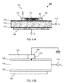
- FIG. 1 is a cross-sectional schematic view illustrating the configuration of the sensors disclosed in PTLS 1 and 2.
- sensor 10 includes: silicon substrate 11; first insulating film 12 formed on one side of silicon substrate 11; second insulating film 13 formed on the other side of silicon substrate 11; channel 14 disposed on first insulating film 12; source electrode 15 connected to one end of channel 14; drain electrode 16 connected to the other end of channel 14; reaction section 17 disposed on second insulating film 13; and gate electrode 18 disposed so as to face second insulating film 13.
- recognition substance 19 such as antibody is immobilized on second insulating film 13.
- Gate electrode 18 is detachable; it is detached when an analyte is fed to reaction section 17 and, when measurement is carried out, it is disposed so as to face second insulating film 13.
- Gate electrode 18 is for example an aluminum plate.
- the sensor disclosed in PTL 1 includes channel 14 formed of carbon nanotubes.
- the sensor disclosed in PTL 2 includes channel 14 formed of a polysilicon film.
- silicon substrate 11, first insulating film 12, second insulating film 13, channel 14, source electrode 15, drain electrode 16, and gate electrode 18 function as back gate-type field-effect transistors.
- a procedure for detecting a detection target substance using sensor 10 illustrated in FIG. 1 will now be described.
- a voltage to be applied to gate electrode 18 is swept with gate electrode 18 being in contact with reaction section 17 (second insulating film 13), and a current value between source electrode 15 and drain electrode 16 is recorded.
- an analyte is fed to reaction section 17 with gate electrode 18 being separated from reaction section 17 (second insulating film 13), allowing the detection target substance contained in the analyte to react with recognition molecules 19 immobilized on second insulating film 13.
- a voltage to be applied to gate electrode 18 is swept with gate electrode 18 being again in contact with reaction section 17 (second insulating film 13), and a current value between source electrode 15 and drain electrode 16 is recorded. Based on the change in current value between before and after analyte feeding as obtained through the above-described procedure, detection of a detection target substance is made possible.
- a cycle of detachment of gate electrode 18 from second insulating film 13 and placement of gate electrode 18 on second insulating film 13 need to be carried out multiple times.
- the state of contact between gate electrode 18 and second insulating film 13 undesirably changes between different cycles.
- gate electrode 18 formed of aluminum plate or the like is placed on second insulating film 13, defects are easily formed in second insulating film 13.
- sensor 10 of the related art such problems as injection of charges into the silicon substrate due to variation in the contact state of the gate electrode and/or to the breakage of the insulating film easily occur. As a consequence, sensor 10 tends to exhibit instable detection precision.
- An object of the present invention is to provide a sensor and a sensor module which are superior in detection precision and detection stability, and a detection method using the same.
- the present invention relates to sensors given below.
- the present invention also relates to detection methods given below.
- the present invention eliminates the need to repeatedly cause the electrodes to contact the reaction section and therefore enables highly precise and stable detection of the presence or absence of a detection target substance or measurement of the concentration of the detection target substance.
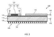
- FIG. 2 is a cross-sectional schematic view illustrating an exemplary configuration of a sensor of the present invention.
- sensor 100 of present invention includes first capacitor electrode 110, first terminal 112, first insulating film 120, second insulating film 130, second capacitor electrode 140, second terminal 142, variable resistance element 150, and reaction section 160.
- First capacitor electrode 110 is a plate-shaped conductor or semiconductor. First capacitor electrode 110 also functions as a substrate of sensor 100. First capacitor electrode 110 is for example an impurity-doped silicon substrate. Other examples of materials for first capacitor electrode 110 include germanium, gallium arsenide (GaAs), indium phosphide (InP), zinc telluride (ZnTe), aluminum, and magnesium. The thickness of first capacitor electrode 110 is not particularly limited and is for example about 0.5 mm.
- First terminal 112 is electrically connected to first capacitor electrode 110. By providing first terminal 112, it is possible to easily connect first capacitor electrode 110 to an external power source.
- the position of first terminal 112 is not particularly limited.
- First terminal 112 is for example disposed on first insulating film 120 (also including the position on the interlayer film formed on first insulating film 120; see FIGS. 5A, 5B , and 7 to 9 ).
- First insulating film 120 is an insulating film disposed on one side of first capacitor electrode 110
- second insulating film 130 is an insulating film disposed on the other side of first capacitor electrode 110.
- First insulating film 120 insulates between first capacitor electrode 110 and second capacitor electrode 140, and between first capacitor electrode 110 and variable resistance element 150.
- First insulating film 120 may be disposed on one side of first capacitor electrode 110 either entirely or partially so long as first insulating film 120 can exert the aforementioned function. Moreover, the thickness of first insulating film 120 may be uniform or may be different at different places.
- Second insulating film 130 insulates between first capacitor electrode 110 and reaction section 160.
- Second insulating film 130 may be disposed on the other side of first capacitor electrode 110 either entirely or partially so long as second insulating film 130 can exert the aforementioned function.
- the thickness of second insulating film 130 may be uniform or may be different at different places.
- the thickness of second insulating film 130 is preferably uniform in an area where reaction section 160 is disposed.
- Each of first insulating film 120 and second insulating film 130 may be a single layer or may be composed of two or more layers.
- First insulating film 120 and second insulating film 130 are for example silicon oxide films.
- Other examples of materials for first insulating film 120 and second insulating film 130 include silicon nitride, aluminum oxide, titanium oxide, acrylic resins, and polyimides.
- the thickness of first insulating film 120 and second insulating film 130 is not particularly limited.
- Second capacitor electrode 140 is a conductor or semiconductor member disposed on first insulating film 120. Second capacitor electrode 140 faces first capacitor electrode 110 across first insulating film 120. First capacitor electrode 110, first insulating film 120 and second capacitor electrode 140 constitutes a capacitor. Second capacitor electrode 140 is for example a film made of polysilicon, metal or alloy. Examples of metals and alloys for second capacitor electrode 140 include aluminum, aluminum alloy, copper, and copper alloy. It is to be noted that when first capacitor electrode 110 is an impurity-doped silicon substrate and second capacitor electrode 140 is an impurity-doped polysilicon film, the impurity doped in first capacitor electrode 110 and the impurity doped in second capacitor electrode 140 may have the same polarity, but preferably have different polarities.
- Variable resistance element 150 is disposed on first insulating film 120 and functions as a transducer.
- Variable resistance element 150 includes base body 152 formed on first insulating film 120, third terminal 154 electrically connected to one end of base body 152, and forth terminal 156 electrically connected to the other end of base body 152.
- base body 152 undergoes a change in resistance value by the influence of isolated charges accumulated in first capacitor electrode 110 and charges in first capacitor electrode 110 which have been induced by the charges generated in reaction section 160.
- Base body 152 is for example a carbon nanotube or a polysilicon film.
- base body 152 may be a lightly doped polysilicon film or a non-doped polysilicon film.
- Third terminal 154 and fourth terminal 156 are for example aluminum films.
- third terminal 154 and fourth terminal 15 may be impurity-doped polysilicon films.
- base body 152 is a lightly doped polysilicon film and third terminal 154 and fourth terminal 156 are impurity-doped polysilicon films, the impurity doped in base body 152 and the impurity doped in third terminal 154 and fourth terminal 156 preferably have the same polarity.
- third terminal 154 and fourth terminal 156 are impurity-doped polysilicon films
- first capacitor electrode 110 is an impurity-doped silicon substrate
- the impurity doped in first capacitor electrode 110 and the impurity doped in third terminal 154 and fourth terminal 156 may have the same polarity, but preferably have different polarities.
- base body 152 is not particularly limited. From the perspective of utilizing the effect of shielding from the outside, base body 152 is preferably surrounded by second capacitor electrode 140. Thus, base body 152 is preferably sized such that it may be surrounded by second capacitor electrode 140.
- Reaction section 160 is disposed on second insulating film 130 and is fed with an analyte which may contain a detection target substance.
- recognition substance 162 capable of reacting with a detection target substance is immobilized on second insulating film 130 in advance.
- the type of recognition substance 162 is not particularly limited so long as it is capable of reacting with a detection target substance.
- Recognition substance 162 may be organic or inorganic substance. Examples of recognition substance 162 include antibody, antigen, enzyme, lectin, and nucleic acid.
- reaction section 160 may be directly disposed on the other side of first capacitor electrode 110.
- recognition substance is immobilized on the other side of first capacitor electrode 110.
- the method of manufacturing sensor 100 is not particularly limited. Sensor 100 may be manufactured by the common manufacturing process for semiconductor devices.
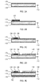
- FIGS. 3A to 3E illustrate an example of a manufacturing process for sensor 100 illustrated in FIG. 2 . It is to be noted that the formation process for first terminal 112 and second terminal 142 are not described herein.
- first insulating film 120 and second insulating film 130 are formed on both sides of first capacitor electrode 110, respectively.
- first capacitor electrode 110 is an impurity-doped silicon substrate
- a silicon oxide film of desired thickness can be formed on the silicon substrate by the thermal oxidation method or the LOCOS method. It is to be noted that when reaction section 160 is directly disposed on the other side of first capacitor electrode 110, second insulating film 130 may not be formed.
- variable resistance element 150 is formed on first insulating film 120 at a predetermined position.
- a rectangular non-doped or lightly doped polysilicon film (base body 152) is formed on first insulating film 120 at a predetermined position ( FIG. 3B ). Further, the opposing ends of the polysilicon film (base body 152) are doped with impurities to form third terminal 154 and fourth terminal 156 ( FIG. 3C ).
- the opposing ends of a lightly doped polysilicon film are doped with impurities to form third terminal 154 and fourth terminal 156
- the impurity doped in base body 152 and the impurity doped in third terminal 154 and fourth terminal 156 preferably have the same polarity.
- first capacitor electrode 110 is an impurity-doped silicon substrate
- the opposing ends of the polysilicon film are preferably doped with an impurity having a polarity different from the polarity of the impurity doped in the silicon substrate.
- third terminal 154 and fourth terminal 156 which are made of metal, may be respectively connected to the opposing ends of the polysilicon film (base body 152) (see FIGS. 5A to FIG. 9 ).
- second capacitor electrode 140 is formed on first insulating film 120 at a predetermined position where second capacitor electrode 140 does not contact variable resistance element 150.
- an impurity-doped polysilicon film or an aluminum film is formed on first insulating film 120 at a predetermined position.
- second insulating film 130 is modified with recognition substance 162 at a predetermined position to form reaction section 160.
- recognition substance 162 For example, antibody is immobilized on second insulating film 130 at a predetermined position. It is to be noted that when reaction section 160 is directly disposed on the other side of first capacitor electrode 110, antibody is immobilized on the other side of first capacitor electrode 110.
- a sensor of the present invention may further include an interlayer film and the like (see FIGS. 5A, 5B , and 7 to 9 ).
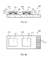
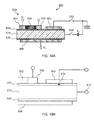
- FIGS. 4A and 4B are cross-sectional schematic views illustrating an exemplary configuration of a sensor module of the present invention.
- FIG. 4A is a cross-sectional schematic view of the sensor module
- FIG. 4B is a plan schematic view of the sensor module.
- sensor module 200 of present invention includes sensor 100 of the present invention and sensor module substrate 210.
- sensor 100 is not illustrated (also in FIGS. 5A and 5B ).
- Sensor module substrate 210 includes connection terminals 212 for connection between sensor 100 and an external device (e.g., power source or measurement device). Connection terminals 212 are electrically connected to fifth terminal 214 and sixth terminal 216 formed on sensor module substrate 210.
- an external device e.g., power source or measurement device.
- Sensor 100 is fixed to sensor module substrate 210 such that variable resistance element 150 and sensor module substrate 210 of sensor 100 face each other. Accordingly, reaction section 160 is exposed to the outside (user side) at all times.
- Third terminal 154 and fourth terminal 156 of variable resistance element 150 are connected and fixed to fifth terminal 214 and sixth terminal 216 of sensor module substrate 210, respectively. Fixation of the terminals is effected for example by the use of conductive binder 220 such as solder or silver paste. Further, in order to ensure more reliable fixation of sensor 100 to sensor module substrate 210, an insulating adhesive may be injected between sensor 100 and sensor module substrate 210 and cured.
- FIGS. 5A and 5B are cross-sectional schematic views illustrating another exemplary configuration of a sensor module of the present invention.
- sensor module 200' may include two sensors 100a, 100b having the same specification and characteristics.
- One sensor 100a is used for detection and the other sensor 100b for reference.
- An external measurement device can utilize a difference value of output between the two sensors 100a, 100b to eliminate influences from the external environment and therefore can achieve highly precise and highly sensitive detection of a detection target substance.
- FIGS. 6A to 6C are cross-sectional schematic views of sensor 100 for explaining the operation principle of sensor 100.
- recognition substance 162 is not illustrated.
- first terminal 112 and second terminal 142 are connected to a power source (connection is indicated by a black circle in the drawings), and a predetermined level of voltage is applied between first capacitor electrode 110 and second capacitor electrode 140.
- application of voltage is preferably effected such that no depletion layer is formed in first capacitor electrode 110 on the first insulating film side and in second capacitor electrode 140 on the first insulating film side.
- first capacitor electrode 110, first insulating film 120 and second capacitor electrode 140 constitute capacitor 170. Accordingly, as illustrated in FIG. 6A , it is possible to accumulate charges, which can be controlled depending solely on the applied voltage and the capacitor value of capacitor 170, in first insulating film 120 and second capacitor electrode 140.
- First terminal 112 and second terminal 142 are then disconnected from the power source (disconnection is indicated by a white circle in the drawings) so that first capacitor electrode 110 and second capacitor electrode 140 are brought into isolated state (not illustrated). This causes the charges accumulated in first capacitor electrode 110 and second capacitor electrode 140 to become isolated charges. The isolated charge greatly affects the detection sensitivity of sensor 100. Accordingly, the voltage to be applied between first capacitor electrode 110 and second capacitor electrode 140 is appropriately determined according to the required detection sensitivity.
- variable resistance element 150 voltage application is indicated by a black circle in the drawings, and a current value between third terminal 154 and fourth terminal 156 and is measured.
- reaction section 160 Next, an analyte is fed to reaction section 160, allowing a detection target substance contained in the analyte to react with recognition molecule 162 immobilized on second insulating film 130. As illustrated in FIG. 6B , this reaction produces charges on second insulating film 130. Further, as illustrated in FIG. 6C , first capacitor electrode 110 is polarized by the electric field generated by the charges produced on second insulating film 130, so that new charges are also induced in first capacitor electrode 110.
- first capacitor electrode is polarized by the electric field generated by the charged produced by a reaction between recognition molecule 162 directly immobilized on the other side of first capacitor electrode 110 and the detection target substance contained in the analyte, so that new charges are induced in first capacitor electrode 110.
- variable resistance element 150 In this state, a predetermined level of voltage (same level as that for the first measurement) is again applied between third terminal 154 and fourth terminal 156 of variable resistance element 150, and a current value between third terminal 154 and fourth terminal 156 is measured.
- the second measurement after analyte feeding may be carried out either before or after the analyte is dried.
- the resistance value of variable resistance element 150 is determined by the electric field formed by the isolate charges accumulated in first capacitor electrode 110.
- variable resistance element 150 is determined by the electric field generated by the isolated charges accumulated in first capacitor electrode 110 and the charges in polarized first capacitor electrode 110 which have been induced by the charges generated in reaction section 160. Accordingly, detection of the presence or absence of the detection target substance or measurement of the concentration of the detection target substance is made possible based on a change in current value between before and after analyte feeding.
- variable resistance element 150 the range within which changes in resistance value show great sensitivity to changes in electric field is generally limited. It is thus required to adjust the amount of isolated charges in first capacitor electrode 110 such that changes in resistance value of variable resistance element 150 show great sensitivity to changes in electric field caused by the reaction in reaction section 160.
- first capacitor electrode 110 and second capacitor electrode 140 it is preferable to remove residual charges in first capacitor electrode 110 and second capacitor electrode 140 immediately before application of a voltage between first capacitor electrode 110 and second capacitor electrode 140. This makes it possible to more precisely control the amount of isolated charges in first capacitor electrode 110.
- first terminal 112 and second terminal 142 of both of detection sensor 100a and reference sensor 100b are connected to a power source, and a predetermined level of voltage is applied between first capacitor electrode 110 and second capacitor electrode 140 simultaneously for both of detection sensor 100a and reference sensor 100b. In this way charges which can be controlled depending solely on the applied voltage and the capacitor value of capacitor 170 can be accumulated in first insulating film 120 and second capacitor electrode 140 of both of sensors 100a, 100b.
- first terminal 112 and second terminal 142 are disconnected from the power source simultaneously for both of sensors 100a, 100b, so that first capacitor electrode 110 and second capacitor electrode 140 are brought into isolated state. This causes the charges accumulated in first capacitor electrode 110 and second capacitor electrode 140 of both of sensors 100a, 100b to become isolated charges.
- a predetermined level of the same voltage is applied between third terminal 154 and fourth terminal 156 of variable resistance element 150 of both of sensors 100a, 100b, and a current value between third terminal 154 and fourth terminal 156 and is measured.
- a difference value between the current value in detection sensor 100a and the current value in reference sensor 100b is then measured.
- offset adjustment is carried out such that the difference value becomes 0 in an external measurement device.
- an analyte is fed to reaction section 160 of detection sensor 100a, allowing the detection target substance contained in the analyte to react with recognition molecules 162 immobilized in reaction section 160. At this point, no analyte is fed to reference sensor 100b.
- a predetermined level of voltage (same voltage in the first measurement) is again applied between third terminal 154 and fourth terminal 156 of variable resistance element 150 of both of sensors 100a, 100b, and a current value between third terminal 154 and fourth terminal 156 is measured.
- the resistance value of variable resistance element 150 is determined by the electric field formed by the isolate charges accumulated in first capacitor electrode 110.
- the resistance value of variable resistance element 150 is determined by the electric field generated by the isolated charges accumulated in first capacitor electrode 110 and the charges in polarized first capacitor electrode 110 which have been induced by the charges generated in reaction section 160.
- the difference value between the current values of sensors 100a, 100b Since the difference value between the current values of sensors 100a, 100b has been adjusted to 0 prior to analyte feeding, the difference value between the current values of sensors 100a, 100b after analyte feeding is such a value that reflects only the effect of the charges generated in reaction section 160 of detection sensor 100a. Furhter, with an external measurement device, the difference between the current values of sensors 100a, 100b may be amplified for improved sensitivity. Accordingly, measurement of a difference value between the current values of sensors 100a, 100b allows for the detection of the presence or absence of the detection target substance or for the measurement of the concentration of the detection target substance.
- sensor 100 and sensor modules 200, 200' of the present invention do not require repetitive contact of electrodes as required in the sensors of the related art (see PTLS 1 and 2) and therefore can detect the presence or absence of a detection target substance or measure the concentration of the detection target substance with high precision and stability. Moreover, sensor 100 and sensor modules 200, 200' of the present invention can easily and stably improve detection sensitivity by adjusting the amount of isolated charges in first capacitor electrode 110.
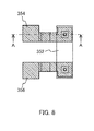
- FIG. 7 is a partially enlarged cross-sectional view of sensor 300 according to Embodiment 1.
- part of first capacitor electrode 310, and the second insulating film and reaction section are not illustrated.
- FIG. 8 is a partially enlarged plan view of a part in FIG. 7 encircled by a broken line. In FIG. 8 , the position of base body 352 is indicated by a broken line.
- the cross-sectional view of FIG. 7 illustrates a cross section of FIG. 8 cut along line A-A.
- sensor 300 includes first capacitor electrode 310, first terminal 312, first insulating film 320, second insulating film (not illustrated), second capacitor electrode 340, second terminal 342, base body 352, third terminal 354, fourth terminal 356, reaction section (not illustrated), and interlayer film 380.
- First capacitor electrode 310 is an impurity-doped silicon substrate.
- First insulating film 320 made of silicon oxide is formed on one side of first capacitor electrode 310, and a second insulating film made of silicon oxide (not illustrated) is formed on the other side of first capacitor electrode 310.
- First insulating film 320 includes thin silicon oxide film 320a formed by the thermal oxidation method, and thick silicon oxide film 320b formed by the LOCOS method. Thin silicon oxide film 320a is formed under base body 352 and second capacitor electrode 340. On the other hand, thick silicon oxide film 320b is formed under first terminal 312 and second terminal 342, and third terminal 354 and fourth terminal 356.
- First terminal 312 is a terminal made of aluminum for connection between first capacitor electrode 310 and an external power source. First terminal 312 is disposed on interlayer film 380 and is electrically connected to first capacitor electrode 310 via contact holes provided in interlayer film 380.
- Second capacitor electrode 340 is a polysilicon film disposed on first insulating film 320.
- First capacitor electrode 310, first insulating film 320 (thin silicon oxide film 320a) and second capacitor electrode 340 constitute a capacitor.
- Second terminal 342 is a terminal made of aluminum for connection between second capacitor electrode 340 and an external power source. Second terminal 342 is disposed on interlayer film 380 and is electrically connected to second capacitor electrode 340 via contact holes provided in interlayer film 380.
- Base body 352 is a non-doped or lightly doped polysilicon film formed on first insulating film 320 (thin silicon oxide film 320a).
- Base body 352, third terminal 354 and fourth terminal 356 constitute variable resistance element 150.
- Interlayer film 380 is an insulating film formed on first insulating film 320, second capacitor electrode 340, and base body 352.
- Interlayer film 380 is for example a silicon oxide film.
- Interlayer film 380 protects base body 352 as well as insulates between members such that the terminals (first terminal 312, second terminal 342, third terminal 354 and fourth terminal 356) are electrically connected only to predetermined members.
- Other examples of materials for interlayer film 380 include silicon nitride, aluminum oxide, hafnium oxide, zirconium oxide, and titanium oxide.
- Third terminal 354 is a terminal made of aluminum for connection between one end of base body 352 and an external power source.
- fourth terminal 356 is a terminal made of aluminum for connection between the other end of base body 352 and an external power source.
- Third terminal 354 and fourth terminal 356 are disposed on interlayer film 380 and are respectively electrically connected to the one end and the other end of base body 352 via contact holes provided in interlayer film 380.
- Sensor 300 according to Embodiment 1 has a large charge injection capacity per unit area compared to sensors 400, 500, 600 according to Embodiments 2 to 4 and therefore can be further downsized. Moreover, since sensor 300 according to Embodiment 1 employs a simple configuration, sensor 300 may be manufactured with fewer steps.
- FIG. 9 is a partially enlarged cross-sectional view of sensor 400 according to Embodiment 2.
- part of first capacitor electrode 310, and second insulating film and reaction section are not illustrated.
- components identical to those of sensor 300 according to Embodiment 1 are given reference signs identical to those for Embodiment 1, and description of such components is not provided.
- sensor 400 includes first capacitor electrode 310, first terminal 312, first insulating film 420, second insulating film (not illustrated), second capacitor electrode 340, second terminal 342, base body 352, third terminal 354, fourth terminal (not illustrated), reaction section (not illustrated), and interlayer film 380.
- First insulating film 420 includes thin silicon oxide film 420a and silicon oxide film 420b which are formed by the thermal oxidation method, and thick silicon oxide film 420c formed by the LOCOS method.
- the thickness of silicon oxide film 420b is larger than the thickness of silicon oxide film 420a.
- Thin silicon oxide film 420a is formed under base body 352.
- Silicon oxide film 420b is formed under second capacitor electrode 340.
- Thick silicon oxide film 420c is formed under first terminal 312, second terminal 342, third terminal 354 and fourth terminal 356.
- First capacitor electrode 310, first insulating film 420 (silicon oxide film 420b formed by the thermal oxidation method) and second capacitor electrode 340 constitute a capacitor.
- first insulating film 420 that contacts second capacitor electrode 340 has a large thickness compared to that of sensor 300 according to Embodiment 1. Thus, it is possible to reduce the defect density in the first insulating film at a portion between first capacitor electrode 310 and second capacitor electrode 340.
- Sensor 400 according to Embodiment 2 has a large charge injection capacity per unit area compared to sensors 500, 600 according to Embodiments 3 and 4 and therefore can be further downsized. Since sensor 400 according to Embodiment 2 employs a simple configuration compared to sensors 500, 600 according to Embodiments 3 and 4, sensor 400 may be manufactured in fewer steps.
- FIG. 10 is a partially enlarged cross-sectional view of sensor 500 according to Embodiment 3.
- part of first capacitor electrode 310, and second insulating film and reaction section are not illustrated.
- components identical to those of sensor 300 according to Embodiment 1 are given reference signs identical to those for Embodiment 1, and description of such components is not provided.
- sensor 500 includes first capacitor electrode 310, first terminal 312, first insulating film 320, second insulating film (not illustrated), second capacitor electrode 540, second terminal 342, base body 352, third terminal 354, fourth terminal (not illustrated), reaction section (not illustrated), first interlayer film 580a, and second interlayer film 580b.
- First interlayer film 580a is an insulating film formed on first insulating film 320 and base body 352.
- First interlayer film 580a is for example a silicon oxide film.
- First interlayer film 580a ensures, together with first insulating film 320 (thin silicon oxide film 320a), reliable insulation between first capacitor electrode 310 and second capacitor electrode 540.
- Other examples of materials for first interlayer film 580a include silicon nitride, aluminum oxide, hafnium oxide, zirconium oxide, and titanium oxide.
- Second capacitor electrode 540 is a polysilicon film formed on first interlayer film 580a.
- First capacitor electrode 310, first insulating film 320 (thin silicon oxide film 320a), first interlayer film 580a and second capacitor electrode 540 constitute a capacitor.
- Second interlayer film 580b is an insulating film formed on second capacitor electrode 540 and first interlayer film 580a.
- Second interlayer film 580b is for example a silicon oxide film.
- Second interlayer film 580b insulates between members such that the terminals (first terminal 312, second terminal 342, third terminal 354, and fourth terminal 356) are electrically connected only to predetermined members.
- Other examples of materials for second interlayer film 580b include silicon nitride, aluminum oxide, hafnium oxide, zirconium oxide, and titanium oxide.
- Sensor 500 according to Embodiment 3 has a small charge injection capacity per unit area compared to sensors 300, 400 according to Embodiments 1 and, but has high capacitor reliability.
- FIG. 11 is a partially enlarged cross-sectional view of sensor 600 according to Embodiment 4.
- part of first capacitor electrode 310, and the second insulating film and reaction section are not illustrated.
- components identical to those of sensor 300 according to Embodiment 1 are given reference signs identical to those for Embodiment 1, and description of such components is not provided.
- sensor 600 includes first capacitor electrode 310, first terminal 312, first insulating film 320, second insulating film (not illustrated), second capacitor electrode 640, second terminal 342, base body 352, third terminal 354, fourth terminal (not illustrated), reaction section (not illustrated), and interlayer film 680.
- Interlayer film 680 is an insulating film formed on first insulating film 320 and base body 352.
- Interlayer film 680 is for example a silicon oxide film.
- Interlayer film 680 protects base body 352 as well as insulates between members such that the terminals (first terminal 312, second terminal 342, third terminal 354, and fourth terminal 356) are electrically connected only to predetermined members.
- Other examples of materials for interlayer film 680 include silicon nitride, aluminum oxide, hafnium oxide, zirconium oxide, and titanium oxide.
- Second capacitor electrode 640 is an aluminum film disposed on interlayer film 680.
- First capacitor electrode 310, first insulating film 320 (thin silicon oxide film 320a), interlayer film 680 and second capacitor electrode 640 constitute a capacitor.
- Sensor 600 according to Embodiment 4 offers high capacitor reliability despite the fact that sensor 600 can be manufactured in the same number of steps as for sensor 300 according to Embodiment 1.
- Embodiments 1 to 4 are directed to examples where second capacitor electrode 340, 540, 640 is disposed beside variable resistance element 150 (base body 352, third terminal 354 and fourth terminal 356), second capacitor electrode 340, 540, 640 may be disposed so as to surround variable resistance element 150.
- FIG. 12 is a plan view of sensor 300, 400, 500, 600 in which second capacitor electrode 340, 540, 640 is disposed so as to surround variable resistance element 150. In this drawing, no interlayer film is illustrated.
- device 700 includes p-type impurity-doped silicon substrate (first capacitor electrode) 710, silicon oxide film (first insulating film) 720 formed on one side of silicon substrate 710, silicon oxide film (second insulating film) 730 formed on the other side of silicon substrate 710, variable resistance element 750 formed on silicon oxide film 720, and backside electrode 760 formed on silicon oxide film 730.
- Variable resistance element 750 was fabricated by doping opposing ends of 30 ⁇ m-width non-doped polysilicon film (base body) 752 with n-type impurities to form third terminal 754 and fourth terminal 756.
- first terminal 712 is formed for connection to a power source for applying charge injection voltage (V c ) between silicon substrate 710, and third terminal 754 and fourth terminal 756.
- backside electrode 760 for applying desired voltage V 2 was provided without forming any reaction section.
- Backside electrode 760 was fabricated by applying silver paste on silicon oxide film 730 and drying the silver paste.
- FIGS. 14A and 14B illustrate two different experimental circuits used in Confirmation Experiments 1 to 3.
- the circuit illustrated in FIG. 14A is for accumulating charges in capacitor 770 formed between silicon substrate 710, and third terminal 754 and fourth terminal 756.
- the circuit illustrated in FIG. 14B is for measuring current I 1 between third terminal 754 and forth terminal 756 after charge accumulation in silicon substrate 710.
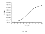
- silicon substrate 710 is in isolated state where it is disconnected from the power source.
- FIG. 15 is a graph of measurement results. This graph confirms that appropriate selection of voltage V c to be applied for accumulating charges in silicon substrate 710 may improve the sensitivity of detecting changes in current (I 1 ) that flows through variable resistance element 750.
- FIG. 16 is a graph of measurement results.
- the graph of FIG. 16 confirms that hysteresis depending on applied voltage V c did not occur, i.e., V 2 -I 1 characteristics were determined solely by applied voltage V c and also good reproducibility was attained.
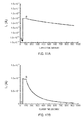
- FIGS. 17A and 17B are graphs of measurement results.
- the numeral range of the vertical axis differs between FIGS. 17A and FIG. 17B .
- “A” denotes the timing of application of voltage V c
- “B” denotes the timing when silicon substrate 710 is brought into isolated state.
- I 1 current flowing through variable resistance element 750, which is determined by charges accumulated in silicon substrate 710, decreases with time. The reason for this would be that the charges accumulated in silicon substrate 710 leaked with time.
- a smaller capacitor value of capacitor 770 in which charges are accumulated would be responsible for vulnerability to leakage of accumulated charges via stray capacitance present in the measurement environment.
- device 800 includes n-type impurity-doped silicon substrate (first capacitor electrode) 810, silicon oxide film (first insulating film) 820 formed on one side of silicon substrate 810, silicon oxide film (second insulating film) 830 formed on the other side of silicon substrate 810, aluminum film (second capacitor electrode) 840 formed on silicon oxide film 820, variable resistance device 850 formed on silicon oxide film 820, and backside electrode 860 formed on silicon oxide film 830.
- Variable resistance element 850 was fabricated by doping the opposing ends of a 2,600 ⁇ m-width non-doped polysilicon film (base body) 852 with p-type impurities to form third terminal 854 and fourth terminal 856.
- first terminal 812 is formed for connection to a power source for applying charge injection voltage (V c ) between silicon substrate 810 and aluminum film 840.
- the area of aluminum film (second capacitor electrode) 840 is such a level that a capacitor can be formed which is arbitrarily large compared to capacitor 770 in device 700 illustrated in FIG. 13A .
- Aluminum film 840 also functions as a second terminal.
- backside electrode 860 for applying desired voltage V 2 was provided without forming any reaction section.
- Backside electrode 860 was fabricated by applying silver paste on silicon oxide film 830 and drying the silver paste.
- FIGS. 19A to 19C illustrate three different experimental circuits used in Confirmation Experiments 4 to 6.
- the circuit illustrated in FIG. 19A is for accumulating charges in capacitor 870 formed between silicon substrate 810 and aluminum film 840.
- the circuit illustrated in FIG. 19B is for measuring current I 1 between third terminal 854 and fourth terminal 856 after charge accumulation in silicon substrate 810.
- silicon substrate 810 is in isolated state where it is disconnected from the power source.
- the circuit illustrated in FIG. 18C is for measuring, after charge accumulation in silicon substrate 810, current I 1 between third terminal 854 and fourth terminal 856 with backside electrode 860 being connected to an external capacitor.
- isolated charges produced by a reaction between the recognition substance and detection target substance in the reaction section are simulated by connecting backside electrode 860 to the external capacitor.
- FIG. 20 is a graph of measurement results. This graph confirms that, as with device 700, appropriate selection of voltage V c to be applied for accumulating charges in silicon substrate 810 may improve the sensitivity of detecting changes in current (I 1 ) that flows through variable resistance element 850. It is to be noted that the orientation of the characteristics curve was different between devices 700 and 800 because the polarity of the impurity doped in silicon substrate 810, the polarity of the impurity doped in third terminal 854 and fourth terminal 856, and the polarity of the applied voltage were opposite to those for device 700.
- FIGS. 21A and 21B are graphs of measurement results.
- the numeral range of the vertical axis differs between FIGS. 21A and FIG. 21B .
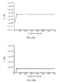
- These graphs confirm that current (I 1 ) flowing through variable resistance element 850, which is determined by charges accumulated in silicon substrate 810, shows little change even when time elapses. The reason for this would be due to the effect of capacitor 870 formed between silicon substrate 810 and aluminum film 840.
- These results confirm that formation of capacitor 870 between silicon substrate 810 and aluminum film 840 eliminates influences of leakage of isolated charges in device 800.
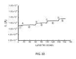
- SW1 and SW2 were connected, SW3 was disconnected, and -2V of voltage V 3 was applied to external capacitor C to accumulate therein negative charges. Thereafter, SW1 and SW2 were disconnected and SW3 was connected so that the charges accumulated in external capacitor C were transferred to backside electrode 860, after which current (I 1 ) between third terminal 854 and fourth terminal 856 was measured with SW3 being disconnected (Measurement No. 3). Switching of voltage to be applied to external capacitor C was carried out every 40 seconds.
- FIG. 22 is a graph of measurement results.
- "A” denotes the timing of application of -1V of V 3
- "B” the timing of application of -2V of V 3
- "C” the timing of application of -3V of V 3
- “D” the timing of application of -4V of V 3 .
- Encircled numbers in FIG. 22 denote measurement numbers.
- This graph confirms that current I 1 flowing through variable resistance element 850 changes according to applied voltage V 3 for accumulating charges in external capacitor C. This means that device 800 can detect charges produced on the backside.
- the sensor according to the present invention is suitable for the detection of infections, confirmation of food safety, detection of environmental contaminants, and so forth.
Landscapes
- Chemical & Material Sciences (AREA)
- Health & Medical Sciences (AREA)
- Engineering & Computer Science (AREA)
- Life Sciences & Earth Sciences (AREA)
- Electrochemistry (AREA)
- Microelectronics & Electronic Packaging (AREA)
- Molecular Biology (AREA)
- Chemical Kinetics & Catalysis (AREA)
- Nanotechnology (AREA)
- Physics & Mathematics (AREA)
- Analytical Chemistry (AREA)
- Biochemistry (AREA)
- General Health & Medical Sciences (AREA)
- General Physics & Mathematics (AREA)
- Immunology (AREA)
- Pathology (AREA)
- Investigating Or Analyzing Materials By The Use Of Electric Means (AREA)
Applications Claiming Priority (2)
| Application Number | Priority Date | Filing Date | Title |
|---|---|---|---|
| JP2012230740 | 2012-10-18 | ||
| PCT/JP2013/006170 WO2014061273A1 (ja) | 2012-10-18 | 2013-10-17 | センサー、センサーモジュールおよび検出方法 |
Publications (2)
| Publication Number | Publication Date |
|---|---|
| EP2910941A1 true EP2910941A1 (de) | 2015-08-26 |
| EP2910941A4 EP2910941A4 (de) | 2016-05-11 |
Family
ID=50487852
Family Applications (1)
| Application Number | Title | Priority Date | Filing Date |
|---|---|---|---|
| EP13847619.7A Withdrawn EP2910941A4 (de) | 2012-10-18 | 2013-10-17 | Sensor, sensormodul und detektionsverfahren |
Country Status (4)
| Country | Link |
|---|---|
| US (2) | US20150192540A1 (de) |
| EP (1) | EP2910941A4 (de) |
| JP (1) | JP6164750B2 (de) |
| WO (1) | WO2014061273A1 (de) |
Families Citing this family (2)
| Publication number | Priority date | Publication date | Assignee | Title |
|---|---|---|---|---|
| JP6296880B2 (ja) * | 2014-04-23 | 2018-03-20 | バイオセンサー株式会社 | 測定装置および測定方法 |
| JPWO2017068610A1 (ja) * | 2015-10-20 | 2018-08-09 | バイオセンサー株式会社 | 測定装置および測定方法 |
Family Cites Families (12)
| Publication number | Priority date | Publication date | Assignee | Title |
|---|---|---|---|---|
| US5605612A (en) * | 1993-11-11 | 1997-02-25 | Goldstar Electron Co., Ltd. | Gas sensor and manufacturing method of the same |
| US20020192653A1 (en) * | 2001-06-13 | 2002-12-19 | Stetter Joseph Robert | Impedance-based chemical and biological imaging sensor apparatus and methods |
| US20060228723A1 (en) * | 2002-01-16 | 2006-10-12 | Keith Bradley | System and method for electronic sensing of biomolecules |
| US7955559B2 (en) * | 2005-11-15 | 2011-06-07 | Nanomix, Inc. | Nanoelectronic electrochemical test device |
| JP4897681B2 (ja) * | 2004-07-23 | 2012-03-14 | エレクトロニック・バイオサイエンシーズ・エルエルシー | イオン・チャネルを通過する時間的に変化する電流を検出するための方法及び装置 |
| WO2006103872A1 (ja) | 2005-03-28 | 2006-10-05 | National University Corporation Hokkaido University | カーボンナノチューブ電界効果トランジスタ |
| CN101287986B (zh) * | 2005-06-14 | 2012-01-18 | 三美电机株式会社 | 场效应晶体管、具备该场效应晶体管的生物传感器及检测方法 |
| WO2007129451A1 (ja) * | 2006-04-26 | 2007-11-15 | National University Corporation NARA Institute of Science and Technology | イメージセンサ |
| TW200914822A (en) * | 2007-05-03 | 2009-04-01 | Koninkl Philips Electronics Nv | Sensor system based on compound with solubility depending on analyte concentration |
| KR100923947B1 (ko) * | 2007-12-10 | 2009-10-29 | 한국전자통신연구원 | 검출 소자 및 검출 시스템 |
| JP5181837B2 (ja) | 2008-05-28 | 2013-04-10 | ミツミ電機株式会社 | センサ及びその製造方法 |
| KR101056385B1 (ko) * | 2008-10-07 | 2011-08-12 | 한국전자통신연구원 | 검출 소자 |
-
2013
- 2013-10-17 EP EP13847619.7A patent/EP2910941A4/de not_active Withdrawn
- 2013-10-17 JP JP2014541952A patent/JP6164750B2/ja active Active
- 2013-10-17 WO PCT/JP2013/006170 patent/WO2014061273A1/ja not_active Ceased
- 2013-10-17 US US14/413,752 patent/US20150192540A1/en not_active Abandoned
-
2018
- 2018-01-03 US US15/861,155 patent/US20180128777A1/en not_active Abandoned
Also Published As
| Publication number | Publication date |
|---|---|
| WO2014061273A1 (ja) | 2014-04-24 |
| EP2910941A4 (de) | 2016-05-11 |
| JPWO2014061273A1 (ja) | 2016-09-05 |
| JP6164750B2 (ja) | 2017-07-19 |
| US20150192540A1 (en) | 2015-07-09 |
| US20180128777A1 (en) | 2018-05-10 |
Similar Documents
| Publication | Publication Date | Title |
|---|---|---|
| US12607595B2 (en) | High sensitivity ISFET sensor | |
| CN112578013B (zh) | 包括生物敏感场效应晶体管的感测电路及操作方法 | |
| US9518953B2 (en) | Ion sensitive detector | |
| US9029132B2 (en) | Sensor for biomolecules | |
| US20140375370A1 (en) | Methods and apparatus for an isfet | |
| US10466199B2 (en) | Biosensor device | |
| US11289601B2 (en) | Negative capacitance semiconductor sensor | |
| CN102132153A (zh) | 减小电子设备中的电容性充电 | |
| US20170336347A1 (en) | SiNW PIXELS BASED INVERTING AMPLIFIER | |
| US20230375499A1 (en) | Biological Device And Biosensing Method Thereof | |
| US20180128777A1 (en) | Sensor, Sensor Module, and Detection Method | |
| US12163992B2 (en) | Charge detection sensor and potential measurement system | |
| JPWO2019131564A1 (ja) | 化学・物理現象の測定装置及びその製造方法 | |
| JP2015206763A (ja) | 測定装置および測定方法 | |
| TW202211381A (zh) | 積體電路及其形成方法 | |
| US20200105996A1 (en) | Piezoelectric biosensor and related method of formation | |
| US20130057304A1 (en) | Capacitive element sensor and method for manufacturing same | |
| US20210270769A1 (en) | Chemical sensor and detection apparatus | |
| JPWO2017068610A1 (ja) | 測定装置および測定方法 | |
| KR20170084387A (ko) | 바이오 센서 | |
| JP2017053794A (ja) | 電気化学センサ |
Legal Events
| Date | Code | Title | Description |
|---|---|---|---|
| PUAI | Public reference made under article 153(3) epc to a published international application that has entered the european phase |
Free format text: ORIGINAL CODE: 0009012 |
|
| 17P | Request for examination filed |
Effective date: 20150108 |
|
| AK | Designated contracting states |
Kind code of ref document: A1 Designated state(s): AL AT BE BG CH CY CZ DE DK EE ES FI FR GB GR HR HU IE IS IT LI LT LU LV MC MK MT NL NO PL PT RO RS SE SI SK SM TR |
|
| AX | Request for extension of the european patent |
Extension state: BA ME |
|
| DAX | Request for extension of the european patent (deleted) | ||
| RA4 | Supplementary search report drawn up and despatched (corrected) |
Effective date: 20160407 |
|
| RIC1 | Information provided on ipc code assigned before grant |
Ipc: G01N 27/414 20060101AFI20160401BHEP Ipc: H01L 29/786 20060101ALI20160401BHEP Ipc: H01L 51/05 20060101ALI20160401BHEP |
|
| 17Q | First examination report despatched |
Effective date: 20170224 |
|
| STAA | Information on the status of an ep patent application or granted ep patent |
Free format text: STATUS: THE APPLICATION IS DEEMED TO BE WITHDRAWN |
|
| 18D | Application deemed to be withdrawn |
Effective date: 20200603 |