EP2905805A1 - Exposure device and exposure method, and device-manufacturing method - Google Patents
Exposure device and exposure method, and device-manufacturing method Download PDFInfo
- Publication number
- EP2905805A1 EP2905805A1 EP13844272.8A EP13844272A EP2905805A1 EP 2905805 A1 EP2905805 A1 EP 2905805A1 EP 13844272 A EP13844272 A EP 13844272A EP 2905805 A1 EP2905805 A1 EP 2905805A1
- Authority
- EP
- European Patent Office
- Prior art keywords
- measurement
- heads
- head group
- movable body
- head
- Prior art date
- Legal status (The legal status is an assumption and is not a legal conclusion. Google has not performed a legal analysis and makes no representation as to the accuracy of the status listed.)
- Granted
Links
- 238000000034 method Methods 0.000 title claims description 64
- 238000004519 manufacturing process Methods 0.000 title claims description 15
- 238000005259 measurement Methods 0.000 claims abstract description 341
- 238000012937 correction Methods 0.000 claims description 36
- 230000000737 periodic effect Effects 0.000 claims description 18
- 238000000926 separation method Methods 0.000 claims description 13
- 230000001678 irradiating effect Effects 0.000 claims description 8
- 238000012423 maintenance Methods 0.000 claims description 3
- 230000008685 targeting Effects 0.000 claims description 3
- 235000012431 wafers Nutrition 0.000 description 281
- JUJBNYBVVQSIOU-UHFFFAOYSA-M sodium;4-[2-(4-iodophenyl)-3-(4-nitrophenyl)tetrazol-2-ium-5-yl]benzene-1,3-disulfonate Chemical compound [Na+].C1=CC([N+](=O)[O-])=CC=C1N1[N+](C=2C=CC(I)=CC=2)=NC(C=2C(=CC(=CC=2)S([O-])(=O)=O)S([O-])(=O)=O)=N1 JUJBNYBVVQSIOU-UHFFFAOYSA-M 0.000 description 100
- 230000003287 optical effect Effects 0.000 description 32
- 238000005286 illumination Methods 0.000 description 19
- 238000001514 detection method Methods 0.000 description 16
- 238000009826 distribution Methods 0.000 description 12
- 230000006870 function Effects 0.000 description 11
- 230000008569 process Effects 0.000 description 9
- 238000012545 processing Methods 0.000 description 9
- 230000010354 integration Effects 0.000 description 8
- 239000004065 semiconductor Substances 0.000 description 8
- 239000000758 substrate Substances 0.000 description 7
- 230000007246 mechanism Effects 0.000 description 6
- 239000011521 glass Substances 0.000 description 5
- 238000001459 lithography Methods 0.000 description 5
- 238000011161 development Methods 0.000 description 4
- 230000018109 developmental process Effects 0.000 description 4
- 239000004973 liquid crystal related substance Substances 0.000 description 4
- 238000006243 chemical reaction Methods 0.000 description 3
- 238000005530 etching Methods 0.000 description 3
- 238000012546 transfer Methods 0.000 description 3
- NAWXUBYGYWOOIX-SFHVURJKSA-N (2s)-2-[[4-[2-(2,4-diaminoquinazolin-6-yl)ethyl]benzoyl]amino]-4-methylidenepentanedioic acid Chemical compound C1=CC2=NC(N)=NC(N)=C2C=C1CCC1=CC=C(C(=O)N[C@@H](CC(=C)C(O)=O)C(O)=O)C=C1 NAWXUBYGYWOOIX-SFHVURJKSA-N 0.000 description 2
- 229910052691 Erbium Inorganic materials 0.000 description 2
- 230000001419 dependent effect Effects 0.000 description 2
- 238000013461 design Methods 0.000 description 2
- 238000010586 diagram Methods 0.000 description 2
- 230000000694 effects Effects 0.000 description 2
- UYAHIZSMUZPPFV-UHFFFAOYSA-N erbium Chemical compound [Er] UYAHIZSMUZPPFV-UHFFFAOYSA-N 0.000 description 2
- 239000000835 fiber Substances 0.000 description 2
- 238000003384 imaging method Methods 0.000 description 2
- 238000009434 installation Methods 0.000 description 2
- 238000013507 mapping Methods 0.000 description 2
- 238000012544 monitoring process Methods 0.000 description 2
- 230000007261 regionalization Effects 0.000 description 2
- 230000001360 synchronised effect Effects 0.000 description 2
- 238000012935 Averaging Methods 0.000 description 1
- 238000000018 DNA microarray Methods 0.000 description 1
- XUIMIQQOPSSXEZ-UHFFFAOYSA-N Silicon Chemical compound [Si] XUIMIQQOPSSXEZ-UHFFFAOYSA-N 0.000 description 1
- 229910052769 Ytterbium Inorganic materials 0.000 description 1
- 230000005856 abnormality Effects 0.000 description 1
- 230000001133 acceleration Effects 0.000 description 1
- 230000009471 action Effects 0.000 description 1
- 238000005452 bending Methods 0.000 description 1
- 230000005540 biological transmission Effects 0.000 description 1
- 239000000919 ceramic Substances 0.000 description 1
- 239000003795 chemical substances by application Substances 0.000 description 1
- 230000003749 cleanliness Effects 0.000 description 1
- 230000001427 coherent effect Effects 0.000 description 1
- 239000000470 constituent Substances 0.000 description 1
- 239000013078 crystal Substances 0.000 description 1
- 238000006073 displacement reaction Methods 0.000 description 1
- 238000010894 electron beam technology Methods 0.000 description 1
- 239000010408 film Substances 0.000 description 1
- 229910052736 halogen Inorganic materials 0.000 description 1
- 150000002367 halogens Chemical class 0.000 description 1
- 238000007654 immersion Methods 0.000 description 1
- 238000007689 inspection Methods 0.000 description 1
- 238000005339 levitation Methods 0.000 description 1
- 239000007788 liquid Substances 0.000 description 1
- 230000000873 masking effect Effects 0.000 description 1
- 239000011159 matrix material Substances 0.000 description 1
- 239000013307 optical fiber Substances 0.000 description 1
- 238000003672 processing method Methods 0.000 description 1
- 230000009467 reduction Effects 0.000 description 1
- 230000004044 response Effects 0.000 description 1
- 229910052710 silicon Inorganic materials 0.000 description 1
- 239000010703 silicon Substances 0.000 description 1
- 239000002210 silicon-based material Substances 0.000 description 1
- 239000000725 suspension Substances 0.000 description 1
- 239000010409 thin film Substances 0.000 description 1
- 230000007704 transition Effects 0.000 description 1
- 239000011800 void material Substances 0.000 description 1
- NAWDYIZEMPQZHO-UHFFFAOYSA-N ytterbium Chemical compound [Yb] NAWDYIZEMPQZHO-UHFFFAOYSA-N 0.000 description 1
Images


Classifications
-
- G—PHYSICS
- G03—PHOTOGRAPHY; CINEMATOGRAPHY; ANALOGOUS TECHNIQUES USING WAVES OTHER THAN OPTICAL WAVES; ELECTROGRAPHY; HOLOGRAPHY
- G03F—PHOTOMECHANICAL PRODUCTION OF TEXTURED OR PATTERNED SURFACES, e.g. FOR PRINTING, FOR PROCESSING OF SEMICONDUCTOR DEVICES; MATERIALS THEREFOR; ORIGINALS THEREFOR; APPARATUS SPECIALLY ADAPTED THEREFOR
- G03F7/00—Photomechanical, e.g. photolithographic, production of textured or patterned surfaces, e.g. printing surfaces; Materials therefor, e.g. comprising photoresists; Apparatus specially adapted therefor
- G03F7/20—Exposure; Apparatus therefor
-
- G—PHYSICS
- G03—PHOTOGRAPHY; CINEMATOGRAPHY; ANALOGOUS TECHNIQUES USING WAVES OTHER THAN OPTICAL WAVES; ELECTROGRAPHY; HOLOGRAPHY
- G03F—PHOTOMECHANICAL PRODUCTION OF TEXTURED OR PATTERNED SURFACES, e.g. FOR PRINTING, FOR PROCESSING OF SEMICONDUCTOR DEVICES; MATERIALS THEREFOR; ORIGINALS THEREFOR; APPARATUS SPECIALLY ADAPTED THEREFOR
- G03F7/00—Photomechanical, e.g. photolithographic, production of textured or patterned surfaces, e.g. printing surfaces; Materials therefor, e.g. comprising photoresists; Apparatus specially adapted therefor
- G03F7/70—Microphotolithographic exposure; Apparatus therefor
- G03F7/70058—Mask illumination systems
- G03F7/70133—Measurement of illumination distribution, in pupil plane or field plane
-
- G—PHYSICS
- G01—MEASURING; TESTING
- G01B—MEASURING LENGTH, THICKNESS OR SIMILAR LINEAR DIMENSIONS; MEASURING ANGLES; MEASURING AREAS; MEASURING IRREGULARITIES OF SURFACES OR CONTOURS
- G01B11/00—Measuring arrangements characterised by the use of optical techniques
-
- G—PHYSICS
- G01—MEASURING; TESTING
- G01B—MEASURING LENGTH, THICKNESS OR SIMILAR LINEAR DIMENSIONS; MEASURING ANGLES; MEASURING AREAS; MEASURING IRREGULARITIES OF SURFACES OR CONTOURS
- G01B11/00—Measuring arrangements characterised by the use of optical techniques
- G01B11/26—Measuring arrangements characterised by the use of optical techniques for measuring angles or tapers; for testing the alignment of axes
-
- G—PHYSICS
- G03—PHOTOGRAPHY; CINEMATOGRAPHY; ANALOGOUS TECHNIQUES USING WAVES OTHER THAN OPTICAL WAVES; ELECTROGRAPHY; HOLOGRAPHY
- G03F—PHOTOMECHANICAL PRODUCTION OF TEXTURED OR PATTERNED SURFACES, e.g. FOR PRINTING, FOR PROCESSING OF SEMICONDUCTOR DEVICES; MATERIALS THEREFOR; ORIGINALS THEREFOR; APPARATUS SPECIALLY ADAPTED THEREFOR
- G03F7/00—Photomechanical, e.g. photolithographic, production of textured or patterned surfaces, e.g. printing surfaces; Materials therefor, e.g. comprising photoresists; Apparatus specially adapted therefor
- G03F7/70—Microphotolithographic exposure; Apparatus therefor
- G03F7/70058—Mask illumination systems
-
- G—PHYSICS
- G03—PHOTOGRAPHY; CINEMATOGRAPHY; ANALOGOUS TECHNIQUES USING WAVES OTHER THAN OPTICAL WAVES; ELECTROGRAPHY; HOLOGRAPHY
- G03F—PHOTOMECHANICAL PRODUCTION OF TEXTURED OR PATTERNED SURFACES, e.g. FOR PRINTING, FOR PROCESSING OF SEMICONDUCTOR DEVICES; MATERIALS THEREFOR; ORIGINALS THEREFOR; APPARATUS SPECIALLY ADAPTED THEREFOR
- G03F7/00—Photomechanical, e.g. photolithographic, production of textured or patterned surfaces, e.g. printing surfaces; Materials therefor, e.g. comprising photoresists; Apparatus specially adapted therefor
- G03F7/70—Microphotolithographic exposure; Apparatus therefor
- G03F7/70691—Handling of masks or workpieces
- G03F7/70775—Position control, e.g. interferometers or encoders for determining the stage position
-
- H—ELECTRICITY
- H01—ELECTRIC ELEMENTS
- H01J—ELECTRIC DISCHARGE TUBES OR DISCHARGE LAMPS
- H01J37/00—Discharge tubes with provision for introducing objects or material to be exposed to the discharge, e.g. for the purpose of examination or processing thereof
- H01J37/30—Electron-beam or ion-beam tubes for localised treatment of objects
- H01J37/304—Controlling tubes by information coming from the objects or from the beam, e.g. correction signals
- H01J37/3045—Object or beam position registration
-
- H—ELECTRICITY
- H01—ELECTRIC ELEMENTS
- H01J—ELECTRIC DISCHARGE TUBES OR DISCHARGE LAMPS
- H01J37/00—Discharge tubes with provision for introducing objects or material to be exposed to the discharge, e.g. for the purpose of examination or processing thereof
- H01J37/30—Electron-beam or ion-beam tubes for localised treatment of objects
- H01J37/317—Electron-beam or ion-beam tubes for localised treatment of objects for changing properties of the objects or for applying thin layers thereon, e.g. for ion implantation
- H01J37/3174—Particle-beam lithography, e.g. electron beam lithography
-
- H—ELECTRICITY
- H01—ELECTRIC ELEMENTS
- H01L—SEMICONDUCTOR DEVICES NOT COVERED BY CLASS H10
- H01L21/00—Processes or apparatus adapted for the manufacture or treatment of semiconductor or solid state devices or of parts thereof
- H01L21/02—Manufacture or treatment of semiconductor devices or of parts thereof
- H01L21/027—Making masks on semiconductor bodies for further photolithographic processing not provided for in group H01L21/18 or H01L21/34
- H01L21/0271—Making masks on semiconductor bodies for further photolithographic processing not provided for in group H01L21/18 or H01L21/34 comprising organic layers
- H01L21/0273—Making masks on semiconductor bodies for further photolithographic processing not provided for in group H01L21/18 or H01L21/34 comprising organic layers characterised by the treatment of photoresist layers
- H01L21/0274—Photolithographic processes
-
- H—ELECTRICITY
- H01—ELECTRIC ELEMENTS
- H01J—ELECTRIC DISCHARGE TUBES OR DISCHARGE LAMPS
- H01J2237/00—Discharge tubes exposing object to beam, e.g. for analysis treatment, etching, imaging
- H01J2237/20—Positioning, supporting, modifying or maintaining the physical state of objects being observed or treated
- H01J2237/202—Movement
-
- H—ELECTRICITY
- H01—ELECTRIC ELEMENTS
- H01J—ELECTRIC DISCHARGE TUBES OR DISCHARGE LAMPS
- H01J2237/00—Discharge tubes exposing object to beam, e.g. for analysis treatment, etching, imaging
- H01J2237/30—Electron or ion beam tubes for processing objects
- H01J2237/317—Processing objects on a microscale
- H01J2237/3175—Lithography
Definitions
- the present invention relates to exposure apparatuses and exposure methods, and device manufacturing methods, and more particularly to an exposure apparatus and an exposure method used in a lithography process for manufacturing microdevices (electronic devices) such as a semiconductor device, and a device manufacturing method which uses the exposure apparatus or the exposure method.
- a projection exposure apparatus of a step-and-repeat method a so-called stepper
- a projection exposure apparatus of a step-and-scan method a so-called scanning stepper (also called a scanner)
- scanning stepper also called a scanner
- an exposure apparatus equipped with a position measurement system that uses a plurality of encoder type sensors (encoder heads) which are mounted on a substrate table.
- the encoder heads measure a position of the substrate table by irradiating measurement beams on a scale which is placed facing the substrate table and receiving return beams from the scale.
- transition from an age of a 300 mm wafer to an age of a 450 mm wafer is near at hand and when it comes to an exposure apparatus handling 450mm wafers, it is considered that while the wafer stage increases in size, the permissible value of the positioning error will become tighter than the present (or around the same as the current level).
- Using the position measurement system according to PTL 1 described above in the exposure apparatus handling 450mm wafers without any changes is considered to be difficult, when considering a further increase in the size of the scale (grating) that accompanies larger wafers.
- a first exposure apparatus which exposes an object with an energy beam and forms a pattern on the object
- the apparatus comprising: a movable body which is movable along a plane including a first axis and a second axis that are orthogonal to each other holding the object, a position measurement system which has a plurality of heads placed at one of the movable body and an outside of the movable body that irradiates a measurement beam from a part of the plurality of heads onto a measurement surface placed on an other of the movable body and the outside of the movable body, receives a return beam from the measurement surface, and measures positional information of the movable body, and a control system which drives the movable body based on the positional information, wherein a one-dimensional or a two-dimensional grating is formed on the measurement surface, the plurality of heads includes a first head group placed within a predetermined plane facing the measurement surface that
- the movable body is driven by the control system, based on positional information obtained by the position measurement system. Further, difference of measurement values in the measurement direction is measured for at least one reference head and the remaining at least two measurement heads, respectively, which are used for obtaining the positional information belonging to the first head group.
- This measurement of the difference by being performed concurrently with the movement of the movable body, allows variation quantity of the grid in the measurement direction of the measurement surface to be monitored, based on data of the difference.
- a second exposure apparatus that exposes an object with an energy beam and forms a pattern on the object
- the apparatus comprising: a movable body which holds the object and is movable along a plane including a first axis and a second axis which are orthogonal to each other; a position measurement system which has a plurality of heads placed at one of the movable body and outside of the movable body that irradiates a measurement beam from a part of the plurality of heads on a measurement surface placed at an other of the movable body and the outside of the movable body, receives a return beam from the measurement surface, and measures positional information of the movable body; and a control system which drives the movable body based on the positional information, wherein one of a one-dimensional and a two-dimensional grating is formed on the measurement surface, and the plurality of heads are placed within a predetermined plane facing the measurement surface and includes a head group including at least two
- a device manufacturing method comprising: forming a pattern on an object using one of the first and the second exposure apparatus described above; and developing the object on which the pattern is formed.
- a first exposure method in which an object is exposed with an energy beam and a pattern is formed on the object, the method comprising: irradiating a measurement beam from a part of a plurality of heads placed on one of a movable body which moves holding the object along a plane including a first axis and a second axis orthogonal to each other and an outside of the movable body on a measurement surface placed on an other of the movable body and the outside of the movable body on which a one-dimensional or a two-dimensional grating is formed, receiving a return beam from the measurement surface, and measuring positional information of the movable body; and driving the movable body based on the positional information that has been obtained, wherein, the plurality of heads includes a first head group, placed within a predetermined plane facing the measurement surface, the heads including at least three heads whose measurement directions are in at least two directions within the predetermined plane and at least one direction orthogonal to the
- the movable body is driven based on the positional information that has been obtained, and concurrently with moving the movable body within the predetermined plane, difference data in the measurement direction of different heads belonging to the first group including difference data of measurement values in the measurement direction of at least one reference head and the remaining at least two measurement heads, respectively, which are used for obtaining the positional information belonging to the first head group are taken in, and based on the difference data which has been taken in, calibration is performed of grid errors in the measurement direction of the measurement surface.
- a second exposure method in which an object is exposed with an energy beam and a pattern is formed on the object, the method comprising: irradiating a measurement beam from a part of a plurality of heads placed on one of a movable body which moves holding the object along a plane including a first axis and a second axis orthogonal to each other and an outside of the movable body on a measurement surface placed on an other of the movable body and the outside of the movable body on which a one-dimensional or a two-dimensional grating is formed, receiving a return beam from the measurement surface, and measuring positional information of the movable body; and driving the movable body based on the positional information that has been obtained, wherein, the plurality of heads includes a head group including at least two heads, placed within a predetermined plane facing the measurement surface, whose measurement directions are in at least one direction of at least two directions within the predetermined plane and a direction orthogonal to
- a device manufacturing method comprising: forming a pattern on the object by one of the first and the second exposure methods described above; and developing the object on which the pattern is formed.
- FIGS. 1 to 10 An embodiment of the present invention will be described, based on FIGS. 1 to 10 .
- FIG. 1 shows a schematic structure of an exposure apparatus 100 related to the embodiment.
- Exposure apparatus 100 is a projection exposure apparatus of a step-and-scan method, or a so-called scanner.
- a projection optical system PL is provided in the present embodiment, and in the description below, the description will be made with a direction parallel to an optical axis AX of projection optical system PL described as a Z-axis direction, a direction in which a reticle and a wafer are relatively scanned within a plane orthogonal to the Z-axis direction described as a Y-axis direction, a direction orthogonal to the Z-axis and the Y-axis described as an X-axis direction, and rotation (tilt) directions around the X-axis, the Y-axis and the Z-axis described as a ⁇ x direction, a ⁇ y direction and a ⁇ z direction, respectively.
- Exposure apparatus 100 is equipped with an illumination system 10, a reticle stage RST which holds a reticle R, a projection unit PU, a wafer stage device 50 including wafer stages WST1, WST2 on which a wafer W is mounted, a control system for these parts and the like.
- Illumination system 10 includes a light source, and an illumination optical system which has an illuminance equalizing optical system including an optical integrator and the like, a reticle blind and the like (each of which are not shown), as is disclosed in, for example, U.S. Patent Application Publication No. 2003/0025890 and the like.
- Illumination system 10 illuminates a slit shaped illumination area IAR on reticle R set (limited) by the reticle blind (masking system) with illumination light (exposure light) IL at an almost equal illuminance.
- illumination light IL an ArF excimer laser beam (wavelength 193nm) is used as an example.
- Reticle stage RST On reticle stage RST, reticle R which has a circuit pattern and the like is formed on its pattern surface (a lower surface in FIG. 1 ) is fixed, for example, by vacuum chucking.
- Reticle stage RST is finely drivable within an XY plane and is drivable in a scanning direction (the Y-axis direction which is a direction orthogonal to the page surface in FIG. 1 ) at a predetermined scanning velocity by a reticle stage driving system 11 (not shown in FIG. 1 , refer to FIG. 9 ) that includes, for example, a linear motor and the like.
- Positional information (including information on position in the ⁇ z direction ( ⁇ z rotation quantity)) of reticle stage RST within the XY plane (movement plane) is constantly detected by a reticle laser interferometer (hereinafter referred to as a "reticle interferometer") 16 shown in FIG. 1 that irradiates a measurement beam on a movable mirror 15 (in practice, a Y movable mirror (or a retroreflector) having a reflection surface orthogonal to the Y-axis direction and an X movable mirror having a reflection surface orthogonal to the X-axis direction are provided), at a resolution of, for example, around 0.25 nm.
- a reticle laser interferometer hereinafter referred to as a "reticle interferometer”
- an encoder system as is disclosed in, for example, U.S. Patent Application Publication No. 2007/0288121 and the like can be used.
- Projection unit PU is placed below reticle stage RST in FIG. 1 (on the -Z side), and is held by a main frame (metrology frame) which structures a part of a body which is not shown.
- Projection unit PU has a barrel 40, and projection optical system PL consisting of a plurality of optical elements held by barrel 40.
- projection optical system PL for example, a dioptric system is used consisting of a plurality of optical elements (lens elements) arranged along an optical axis AX parallel to the Z-axis direction.
- Projection optical system PL for example, is double telecentric, and has a predetermined projection magnification (such as, for example, 1/4 times, 1/5 times or 1/8 times).
- illumination area IAR is illuminated by illumination light IL from illumination system 10
- illumination light IL which has passed reticle R which is placed so that its pattern surface almost coincides with a first plane (an object plane) of projection optical system PL
- a reduced image of a circuit pattern of reticle R within illumination area IAR is formed via projection optical system PL, on an area (exposure area) IA conjugate with illumination area IAR on wafer W which has its surface coated with a resist (a sensitive agent) that is placed on a second plane (image plane) side of projection optical system PL.
- the pattern of reticle R is generated on wafer W by illumination system 10 and projection optical system PL, and the pattern is formed on wafer W by exposing a sensitive layer (a resist layer) on wafer W by illumination light IL.
- the main frame can either be of a conventional gate type, or a suspension support type as is disclosed in, for example, U.S. Patent Application Publication No. 2008/0068568 and the like.
- a scale plate 21 is placed parallel to the XY plane, for example, at a height substantially flush with the lower end surface of barrel 40.
- Scale plate 21 in the present embodiment as is shown in FIG. 2 is structured, for example, from four L-shaped sections (components) 21 1 , 21 2 , 21 3 and 21 4 , and in the center, for example, a rectangular-shaped opening 21a is formed into which the - Z side end of barrel 40 is inserted.
- the width of scale plate 21 in the X-axis direction and in the Y-axis direction are a and b, respectively, and the width of opening 21a in the X-axis direction and in the Y-axis direction are ai and bi, respectively.
- a scale plate 22 is placed substantially flush with scale plate 21.
- Scale plate 22, as is shown in FIG. 3 is also structured, for example, from four L-shaped sections (components) 22 1 , 22 2 , 22 3 and 22 4 , and in the center, for example, a rectangular-shaped opening 22a is formed into which the - Z side end of an alignment system ALG which will be described later is inserted.
- the width of scale plate 22 is a in the X-axis direction and is b in the Y-axis direction, respectively, and the width of opening 22a is ai in the X-axis direction and is bi in the Y-axis direction, respectively.
- the width of scale plates 21, 22 and the width of openings 21a, 22a were the same in the X-axis and the Y-axis directions, respectively, the width does not necessarily have to be the same, and the width can be different in at least one of the X-axis and the Y-axis directions.
- scale plates 21, 22 are supported in a suspended manner by the main frame (metrology frame) which is not shown supporting projection unit PU and alignment system ALG.
- main frame metal frame
- projection unit PU and alignment system ALG On a lower surface (-Z side surface) of scale plates 21, 22, a reflection type two-dimensional grating RG (refer to FIGS.
- a grating that has a predetermined pitch of, for example, 1 ⁇ m having a periodic direction in a -45 degrees direction (a -135 degrees direction when the Y-axis serves as a reference) with the X-axis serving as a reference, and a grating that has a predetermined pitch of, for example, 1 ⁇ m having a periodic direction in a 45 degrees direction (a -45 degrees direction when the Y-axis serves as a reference) with the X-axis serving as a reference.
- Two-dimensional grating RG of scale plates 21, 22 covers at least a movement range of wafer stages WST1, WST2 at the time of exposure operation and at the time of alignment (measurement), respectively.
- Wafer stage device 50 as is shown in FIG. 1 , is equipped with a stage base 12 supported substantially horizontal on a floor surface by a plurality of (for example, three or four) vibration-proof mechanisms (omitted in drawings), wafer stages WST1, WST2 placed on stage base 12, a wafer stage driving system 27 (only a part of the system is shown in FIG. 1 , refer to FIG. 9 ) for driving wafer stages WST1, WST2, and a measurement system and the like which measures a position of wafer stages WST1, WST2.
- the measurement system is equipped with encoder systems 70, 71 and a wafer laser interferometer system (hereinafter shortly referred to as wafer interferometer system) 18 and the like shown in FIG. 9 .
- encoder systems 70, 71 and wafer interferometer system 18 will be described furthermore later in the description.
- wafer interferometer system 18 does not necessarily have to be provided.
- Stage base 12 is made up of a member that has a plate-like outer shape, and its upper surface is finished to a high flatness and serves as a guide surface when wafer stages WST1, WST2 move.
- a coil unit is housed that includes a plurality of coils 14a placed in a shape of a matrix with an XY two-dimensional direction serving as a row direction and a column direction.
- stage base 12 can be provided to support stage base 12 in a levitated manner separately so that stage base 12 functions as a counter mass (reaction force canceller) which moves according to the momentum conservation law by an action of a reaction force of the driving force of wafer stages WST1, WST2.
- Wafer stage WST1 as is shown in FIG. 1 , has a stage main section 91, and a wafer table WTB1 which is placed above stage main section 91 and is supported in a non-contact manner with respect to stage main section 91 by a Z tilt driving mechanism 32a (not shown in FIG. 1 , refer to FIG. 9 ).
- wafer stage WST2 as is shown in FIG. 1 , has stage main section 91, and a wafer table WTB2 which is placed above stage main section 91 and is supported in a non-contact manner with respect to stage main section 91 by a Z tilt driving mechanism 32b (not shown in FIG. 1 , refer to FIG. 9 ).
- wafer stage WST2 and wafer stage WST1 are structured similarly, hereinafter, wafer stage WST1 will be discussed and described representatively.
- Wafer table WTB1 is supported in a non-contact manner by Z tilt driving mechanism 32a by adjusting a balance of an upward force (repulsive force) such as an electromagnetic force and a downward force (a gravitational force) including self-weight at three points, and is finely driven at least in directions of three degrees of freedom which are the Z-axis direction, the ⁇ x direction, and the ⁇ y direction.
- a slider section 91a is provided at a bottom section of stage main section 91.
- Slider section 91a has a magnet unit consisting of a plurality of magnets having an XY two-dimensional arrangement within the XY plane, a housing which houses the magnet unit, and a plurality of air bearings provided at a periphery of a bottom surface of the housing.
- the magnet unit structures a planar motor 30 along with the coil unit previously described that performs an electromagnetic force (Lorentz force) drive as is disclosed in, for example, U.S. Patent No. 5,196,745 and the like.
- planar motor 30 the motor is not limited to a planar motor of the Lorentz force driving method, and a planar motor of a variable magneto-resistance driving method can also be used.
- Wafer stage WST1 is supported in a levitated manner by a predetermined clearance (clearance/spacing/void (gap)/spatial distance) on stage base, for example, via a clearance of around several ⁇ m by the plurality of air bearings described above, and is driven in the X-axis direction, the Y-axis direction and the ⁇ z direction by planar motor 30.
- a predetermined clearance curviation/spacing/void (gap)/spatial distance
- wafer table WTB1 (wafer W) can be driven in directions of six degrees of freedom (the X-axis direction, the Y-axis direction, the Z-axis direction, the ⁇ x direction, ⁇ y direction and the ⁇ z direction (hereinafter shortly described as X, Y, Z, ⁇ x, ⁇ y, and ⁇ z)) with respect to stage base 12.
- the X-axis direction, the Y-axis direction, the Z-axis direction, the ⁇ x direction, ⁇ y direction and the ⁇ z direction hereinafter shortly described as X, Y, Z, ⁇ x, ⁇ y, and ⁇ z
- wafer stage driving system 27 is structured including a pair of planar motors 30 having a common stator (coil unit) which drives each of wafer stages WST1 and WST2, and Z tilt driving mechanisms 32a, 32b that wafer stages WST1 and WST2 are equipped with, respectively.
- planar motor 30 is not limited to a motor of a moving magnet method, and can also be a motor of a moving coil method. Further, as planar motor 30, a planar motor of a magnetic levitation method can also be used. In this case, the air bearings previously described do not have to be provided.
- wafer stage WST1 can be driven in directions of six degrees of freedom by planar motor 30. Further, wafer table WTB1 can be finely driven in at least one direction of the X-axis direction, the Y-axis direction, and the ⁇ z direction. That is, wafer stage WST1 can be structured by a coarse/fine movement stage.
- wafer W is mounted via a wafer holder which is not shown, and is fixed by a chuck mechanism which is not shown, for example, by vacuum chucking (or electrostatic suction).
- a chuck mechanism which is not shown, for example, by vacuum chucking (or electrostatic suction).
- one or a plurality of reference mark members is provided on which a plurality of reference marks such as a pair of first reference marks and a second reference mark are formed that are detected by a pair of reticle alignment systems 13A, 13B and alignment system ALG, respectively.
- Encoder systems 70, 71 obtain (measure) positional information of wafer tables WTB1, WTB2 in directions of six degrees of freedom (X, Y, Z, ⁇ x, ⁇ y, ⁇ z) in a movement area at the time of exposure including an area directly below projection optical system PL and a movement area at the time of measurement including an area directly below alignment system ALG, respectively.
- X, Y, Z, ⁇ x, ⁇ y, ⁇ z degrees of freedom
- movement area at the time of exposure is an area in which the wafer stage is moved during an exposure operation within an exposure station (a first area) where exposure of the wafer is performed via projection optical system PL, and the exposure operation, for example, is not only exposure of all shot areas on the wafer onto which the pattern should be transferred, but also includes preparatory operations for the exposure (for example, detection of reference marks previously described) and the like.
- Movement area at the time of measurement is an area in which the wafer stage is moved during a measurement operation within a measurement station (a second area) where measurement of the positional information is performed by detection of alignment marks of the wafer by alignment system ALG, and the measurement operation, for example, is not only detection of a plurality of alignment marks on the wafer, but also includes detection of reference marks by alignment system ALG (furthermore, measurement of positional information (height difference information) of the wafer in the Z-axis direction) and the like.
- a first encoder head group 61 1 In wafer tables WTB1, WTB2, as is shown in the planar view in FIGS. 2 and 3 , with a center of the upper surface serving as an origin point (coincides with the center of wafer W), a first encoder head group 61 1 , a second encoder head group 61 2 , a third encoder head group 61 3 , and a fourth encoder head group 61 4 are placed in a part of each corner of a first quadrant, a second quadrant, a third quadrant and a fourth quadrant.
- the encoder head group will be shortly described as a head group.
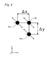
- the first head group 61 1 includes three encoder heads (hereinafter appropriately referred to as heads) 60 1 , 60 1a , 60 1b placed in the corner section at the +X side and the +Y side on the upper surface of wafer tables WTB1, WTB2.
- the three heads 60 1 , 60 1a , 60 1b in the present embodiment are placed at each apex position of a right triangle.
- head 60 1 is provided at the vicinity of the corner (apex) at the +X side and the +Y side on the upper surface of wafer tables WTB1, WTB2.
- Head 60 1a is placed at a point shifted by ⁇ x in a -X direction from an installation position of head 60 1 .
- head 60 1b is placed at a point shifted by ⁇ y in a -Y direction from an installation position of head 60 1 .
- the second head group 61 2 includes three heads 60 2 , 60 2a , 60 2b placed in the corner section at the -X side and the +Y side on the upper surface of wafer tables WTB1, WTB2.
- the three heads 60 2 , 60 2a , 60 2b in the present embodiment are provided in an arrangement symmetrical to the three heads 60 1 , 60 1a , 60 1b on wafer tables WTB1, WTB2, with respect to a straight line (center line) parallel to the Y-axis that passes through the center of the upper surface (the origin point described above).
- the third head group 61 3 includes three heads 60 3 , 60 3a , 60 3b placed in the corner section at the -X side and the -Y side on the upper side of wafer tables WTB1, WTB2.
- the three heads 60 3 , 60 3a , 60 3b in the present embodiment are provided in an arrangement symmetrical (point symmetric) to the three heads 60 1 , 60 1a , 60 1b on wafer tables WTB1, WTB2, with respect to the center of the upper surface.
- the fourth head group 61 4 includes three heads 60 4 , 60 4a , 60 4b placed in the corner section at the +X side and the -Y side on the upper surface of wafer table WTB1, WTB2.
- the three heads 60 4 , 60 4a , 60 4b in the present embodiment are provided in an arrangement symmetrical to the three heads 60 1 , 60 1a , 60 1b on wafer tables WTB1, WTB2, with respect to a straight line (center line) parallel to the X-axis that passes through the center of the upper surface.
- a separation distance between heads 60 1 and 60 2 in the X-axis direction and the separation distance between heads 60 3 and 60 4 in the X-axis direction are equally A.
- a separation distance between heads 60 1 , 60 4 in the Y-axis direction and the separation distance between heads 60 2 and 60 3 in the Y-axis direction are equally B.
- These separation distances A, B are larger than widths ai, bi of opening 21a of scale plate 21. In a precise sense, A ⁇ ai+2t, B ⁇ bi+2t, taking into consideration width t of the non-effective area previously described.
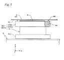
- Each of head 60 1 to 60 4 , 60 1a to 60 4a , and 60 1b to 60 4b , as is shown representatively taking up head 60 1 in FIG. 5 , are each housed inside holes of a predetermined depth in the Z-axis direction formed in wafer tables WTB1, WTB2.
- Heads 60 1 , 60 1a , 60 1b belonging to the first head group 61 1 are two-dimensional heads whose measurement directions are in a direction of 135 degrees (-45 degrees) with the X-axis as a reference and in the Z-axis direction.
- heads 60 3 , 60 3a , 60 3b belonging to the third head group 61 3 are two-dimensional heads whose measurement directions are in the direction of 135 degrees (-45 degrees) with the X-axis as a reference and in the Z-axis direction.
- Heads 60 2 , 60 2a , 60 2b belonging to the second head group 61 2 are two-dimensional heads whose measurement directions are in a direction of 45 degrees (-135 degrees) with the X-axis as a reference and in the Z-axis direction.
- heads 60 4 , 60 4a , 60 4b belonging to the fourth head group 61 4 are two-dimensional heads whose measurement directions are in the direction of 45 degrees (-135 degrees) with the X-axis as a reference and in the Z-axis direction.
- two-dimensional grating RG formed on the surface of sections 21 1 , 21 2 , 21 3 , 21 4 of scale plate 21, or sections 22 1 , 22 2 , 22 3 , 22 4 of scale plate 22 opposing the heads, and receiving reflection/diffraction beams from two-dimensional grating RG.
- a sensor head having a structure similar to a displacement measurement sensor head disclosed in, for example, U.S. Patent No. 7, 561, 280 can be used.
- the light source and the photodetector are provided external to each head, or to be more specific, provided inside (or outside) stage main section 91, and only the optical system is provided inside each head. Then, the light source, the photodetector and the optical system are optically connected via an optical fiber which is not shown.
- aerial transmission of laser beams and the like can be performed between stage main section 91 and wafer table WTB1 (or WTB2).
- heads 60 1 , 60 1a , 60 1b belonging to the first head group 61 1 structure two-dimensional encoders 70 1 , 70 1a , 70 1b , and 71 1 , 71 1a , 71 1b (refer to FIG.
- heads 60 2 , 60 2a , 60 2b belonging to the second head group 61 2 structure two-dimensional encoder 70 2 , 70 2a , 70 2b , and 71 2 , 71 2a , 71 2b (refer to FIG.
- heads 60 3 , 60 3a , 60 3b belonging to the third head group 61 3 structure two-dimensional encoders 70 3 , 70 3a , 70 3b , and 71 3 , 71 3a , 71 3b (refer to FIG.
- heads 60 4 , 60 4a , 60 4b belonging to the fourth head group 61 4 structure two-dimensional encoders 70 4 , 70 4a , 70 4b , and 71 4 , 71 4a , 71 4b (refer to FIG. 9 ) that irradiate measurement beams (measurement light) on (section 21 4 of) scale plate 21, receive diffraction beams from a grating formed on a surface (lower surface) of scale plate 21 having a periodic direction in the 45 degrees direction ( ⁇ direction), and measure the position of wafer tables WTB1, WTB2 in the 45 degrees direction ( ⁇ direction) and the Z-axis direction.
- heads 60 1 , 60 1a , 60 1b belonging to the first head group 61 1 structure two-dimensional encoders 70 1 , 70 1a , 70 1b , and 71 1 , 71 1a , 71 1b (refer to FIG.
- heads 60 2 , 60 2a , 60 2b belonging to the second head group 61 2 structure two-dimensional encoders 70 2 , 70 2a , 70 2b , and 71 2 , 71 2a , 71 2b (refer to FIG. 9 ) that irradiate measurement beams (measurement light) on (section 22 2 of) scale plate 22, receive diffraction beams from a grating formed on a surface (lower surface) of scale plate 22 having a periodic direction in the 45 degrees direction ( ⁇ direction), and measure the position of wafer tables WTB1, WTB2 in the 45 degrees direction ( ⁇ direction) and the Z-axis direction.
- heads 60 3 , 60 3a , 60 3b belonging to the third head group 61 3 structure two-dimensional encoders 70 3 , 70 3a , 70 3b , and 71 3 , 71 3a , 71 3b (refer to FIG.
- heads 60 4 , 60 4a , 60 4b belonging to the fourth head group 61 4 structure two-dimensional encoders 70 4 , 70 4a , 70 4b , and 71 4 , 71 4a , 71 4b (refer to FIG. 9 ) that irradiate measurement beams (measurement light) on (section 22 4 of) scale plate 22, receive diffraction beams from a grating formed on a surface (lower surface) of scale plate 22 having a periodic direction in the 45 degrees direction ( ⁇ direction), and measure the position of wafer tables WTB1, WTB2 in the 45 degrees direction ( ⁇ direction) and the Z-axis direction.
- heads 60 1 , 60 1a , 60 1b , 60 2 , 60 2a , 60 2b , 60 3 , 60 3a , 60 3b , 60 4 , 60 4a and 60 4b on wafer stage WST1 structure two-dimensional encoders 70 1 , 701 a, 70 1b , 70 2 , 70 2a , 70 2b , 70 3 , 70 3a , 70 3b , 70 4 , 70 4a , 70 4b , respectively, along with the scale plates on which the measurement beam (measurement light) is irradiated, and heads 60 1 , 60 1a , 60 1b , 60 2 , 60 2a , 60 2a , 60 2a , 60
- Measurement values of the two-dimensional encoders (hereinafter shortly referred to as an encoder as appropriate) 70 1 , 70 1a , 70 1b , 70 2 , 70 2a , 70 2b , 70 3 , 70 3a , 70 3b , 70 4 , Il, 70 4b , 71 1 , 71 1a , 71 1b , 71 2 , 71 2a , 71 2b , 71 3 , 71 3a , 71 3b , 71 4 , 71 4a , 71 4b are each supplied to main controller 20 (refer to FIG. 9 ).
- main controller 20 obtains positional information of wafer tables WTB1, WTB2 in directions of six degrees of freedom (X, Y, Z, ⁇ x, ⁇ y, ⁇ z) within the movement area at the time of exposure including the area directly below projection optical system PL, based on the measurement values of at least three encoders (that is, at least three encoders that output effective measurement values) that face lower surface of (sections 21 1 to 21 4 which structure) scale plate 21 on which two-dimensional grating RG is formed.
- Main controller 20 performs calibration (to be described later on) of a grid (grid error) of a coordinate system at the time of exposure that corresponds to a variation of two-dimensional grating RG of scale plate 21 while wafer tables WTB1, WTB2 move within the movement area at the time of exposure including, for example, when exposure is being performed, using the measurement values of all of the heads in at least the three groups to which the heads of at least the three encoders belong used for measuring the positional information of wafer tables WTB1, WTB2 in directions of six degrees of freedom (X, Y, Z, ⁇ x, ⁇ y, ⁇ z).
- main controller 20 obtains positional information of wafer tables WTB1, WTB2 in directions of six degrees of freedom (X, Y, Z, ⁇ x, ⁇ y, ⁇ z) within the movement area at the time of measurement including the area directly below alignment system ALG, based on the measurement values of at least three encoders (that is, at least three encoders that output effective measurement values) that face the lower surface of (sections 22 1 to 22 4 which structure) scale plate 22 on which two-dimensional grating RG is formed.
- Main controller 20 can perform calibration (to be described later on) of a grid (grid error) of a coordinate system at the time of measurement that corresponds to a variation of two-dimensional grating RG of scale plate 22 while wafer tables WTB1, WTB2 move within the movement area at the time of measurement, including, for example, when alignment is being performed, using the measurement values of all of the heads in at least the three groups to which the heads of at least the three encoders belong used for measuring the positional information of wafer tables WTB1, WTB2 in directions of six degrees of freedom (X, Y, Z, ⁇ x, ⁇ y, ⁇ z).
- the position of wafer stages WST1, WST2 can be measured by wafer interferometer system 18 (refer to FIG. 9 ), independently from encoder systems 70, 71.
- the measurement values of wafer interferometer system 18 are used secondarily, for example, as a backup and the like at the time of output abnormalities of encoder systems 70, 71. Incidentally, details on wafer interferometer system 18 are omitted.
- Alignment system ALG is an alignment system of an off-axis method that is placed in a predetermined spacing on the +X side of projection optical system PL.
- alignment system ALG as an example, an FIA (Field Image Alignment) system is used which is a type of an alignment sensor of an image-processing method that measures a mark position by illuminating a mark with a broadband (wideband) light such as a halogen lamp and the like, and performing image-processing on this mark image.
- Imaging signals from alignment system ALG are supplied to main controller 20 (refer to FIG. 9 ), via an alignment signal processing system which is not shown.
- alignment system ALG is not limited to the FIA system, and for example, it is a matter of course that an alignment sensor which performs detection by irradiating a coherent detection light on a mark and detecting scattered light or diffracted light generated from the mark, or by making two diffracted lights (for example, diffracted light of the same order or diffracted light diffracting in the same direction) generated from the mark interfere with each other can be used alone, or appropriately combined.
- alignment system ALG an alignment system that has a plurality of detection areas as in the one disclosed in, for example, U.S. Patent Application Publication No. 2008/0088843 and the like can be employed.
- a multi-point focal point detection system of an oblique incidence method (hereinafter, shortly described as multi-point AF system) AF (not shown in FIG. 1 , refer to FIG. 9 ) is provided placed at the measurement station along with alignment system ALG and having a structure similar to the one disclosed in, for example, U.S. Patent No. 5, 448, 332 and the like. At least a part of a measurement operation by multi-point AF system AF is performed concurrently with the mark detection operation by alignment system ALG, and positional information of the wafer table is measured by the encoder system previously described during the measurement operation. Detection signals of multi-point AF system AF is supplied to main controller 20 (refer to FIG.
- Main controller 20 detects positional information (height difference information/unevenness information) of the wafer W surface in the Z-axis direction, based on the detection signals of multi-point AF system AF and the measurement information of the encoder system previously described, and performs a so-called focus/leveling control of wafer W during scanning exposure in the exposure operation based on the information detected beforehand and the measurement information of the encoder system previously described (positional information in the Z-axis, the ⁇ x and the ⁇ y directions).
- the multi-point AF system can be provided at the vicinity of projection unit PU within exposure station, and focus/leveling control of wafer W may be performed driving the wafer table while measuring the positional information (unevenness information) of the wafer surface at the time of the exposure operation.
- a pair of reticle alignment systems 13A, 13B (not shown in FIG. 1 , refer to FIG. 9 ) of a TTR (Through The Reticle) method which uses light of the exposure wavelength as is disclosed in, for example, U.S. Patent No. 5,646,413 and the like, is provided above reticle R.
- Detection signals of reticle alignment systems 13A, 13B are supplied to main controller 20, via an alignment signal processing system which is not shown.
- reticle alignment can be performed using the aerial image measuring instrument which is not shown provided on wafer stage WST.
- FIG. 9 shows a block diagram which is partly omitted of a control system related to stage control of exposure apparatus 100.
- This control system is structured centering on main controller 20.
- Main controller 20 includes a so-called microcomputer (or a workstation) consisting of a CPU (Central Processing Unit), a ROM (Read Only Memory), a RAM (Random Access Memory) and the like that has overall control of the entire device.
- CPU Central Processing Unit
- ROM Read Only Memory
- RAM Random Access Memory
- one of wafer stages WST1, WST2 on which the wafer is loaded is moved within the measurement station (movement area at the time of measurement) by main controller 20, and wafer measurement operation is performed by alignment system ALG and multi-point AF system. That is, to wafer W held by one of wafer stages WST1, WST2 within the movement area at the time of measurement, mark detection using alignment system ALG, or a so-called wafer alignment (such as Enhanced Global Alignment (EGA) disclosed in, for example, U.S. Patent No. 4, 780, 617 and the like) and measurement of surface information (height difference/unevenness information) of the wafer using the multi-point AF system are performed.
- EGA Enhanced Global Alignment
- positional information of wafer tables WTB1, WTB2 in directions of six degrees of freedom (X, Y, Z, ⁇ x, ⁇ y, ⁇ z) is obtained (measured).
- position of the second reference mark on the reference mark member provided on one of wafer stages WST1, WST2 is measured by main controller 20 using alignment system ALG. Then, array coordinates of a plurality of shot areas on wafer W calculated as results of wafer alignment are replaced with array coordinates using the second reference mark as a reference.
- one of the wafer stages moves to the movement area at the time of exposure, and by main controller 20, reticle alignment and the like to obtain a positional relation between a projection center of the reticle pattern and the center of the pair of the first reference marks is performed, using reticle alignment systems 13A, 13B, reference mark members (not shown) on the wafer table (WTB1 or WTB2) and the like in a procedure similar to a normal scanning stepper.
- main controller 20 based on the results of the reticle alignment and the array coordinates of the plurality of shot areas using the second reference marks obtained as a result of the wafer alignment as a reference, exposure operation by the step-and-scan method is performed, and the pattern of reticle R is transferred, respectively, onto a plurality of shot areas on wafer W.
- the exposure operation by the step-and-scan method is performed by alternately repeating a scanning exposure operation in which synchronous movement of reticle stage RST and wafer stage WST1 or WST2 is performed, and a movement (stepping) operation between shots in which wafer stage WST1 or WST2 is moved to an acceleration starting position for exposure of a shot area.
- positional information in directions of six degrees of freedom (X, Y, Z, ⁇ x, ⁇ y, ⁇ z) of one of the wafer tables (WTB1 or WTB2) is obtained (measured) by encoder system 70 (encoders 70 1 to 70 4 ) or encoder system 71 (encoders 71 1 to 71 4 ).
- exposure apparatus 100 of the present embodiment is equipped with the two wafer stages WST1, WST2. Therefore, concurrently with performing exposure by the step-and-scan method on the wafer loaded on one of wafer stages, for example, wafer stage WST1, a concurrent processing operation is performed in which wafer alignment and the like is performed on the wafer mounted on the other wafer stage WST2.
- main controller 20 obtains (measures) positional information of wafer table WTB1 in directions of six degrees of freedom (X, Y, Z, ⁇ x, ⁇ y, ⁇ z) using encoder system 70 (refer to FIG. 9 ) in both the movement area at the time of exposure and the movement area at the time of measurement. Further, main controller 20 obtains (measures) positional information of wafer table WTB2 in directions of six degrees of freedom (X, Y, Z, ⁇ x, ⁇ y, ⁇ z) using encoder system 71 (refer to FIG. 9 ) in both the movement area at the time of exposure and the movement area at the time of measurement.
- measurement values of encoder heads 60 1 to 60 4 or encoders 70 1 to 70 4 mean measurement values in a measurement direction which is not in the Z-axis direction of encoder heads 60 1 to 60 4 or encoders 70 1 to 70 4 .
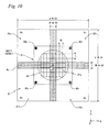
- FIG. 10 shows a relation between a placement of encoder heads 60 1 to 60 4 and each section 21 1 to 21 4 of scale plate 21 on wafer stage WST1 and measurement areas A 0 to A 4 of encoder system 70.
- FIG. 10 shows only heads 60 1 , 60 2 , 60 3 , and 60 4 which are used for measuring positional information in directions of six degrees of freedom of wafer table WTB1.
- wafer stage WST2 is structured similarly to wafer stage WST1, the description here will be made only for wafer stage WST1.
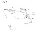
- first area A 1 which is within the movement area at the time of exposure that is also an area located on the +X side and on the +Y side with respect to exposure center (the center of exposure area IA) P (an area within the first quadrant (however, excluding an area A 0 ) whose origin point is exposure center P)
- heads 60 4 , 60 1 , 60 2 on wafer stage WST1 face sections 21 4 , 21 1 , 21 2 of scale plate 21, respectively.
- effective measurement values are sent to main controller 20 from heads 60 4 , 60 1 , 60 2 (encoders 70 4 , 70 1 , 70 2 ).
- the position of wafer stages WST1, WST2 in the description below means the position in the center of the wafer stage (coincides with the center of wafer table and the center of the wafer, respectively). That is, instead of using the expression, the position in the center of wafer stages WST1, WST2, the expression used will be, the position of wafer stages WST1, WST2.
- wafer stage WST1 is positioned within a second area A 2 which is within the movement area at the time of exposure that is also an area located on the -X side and on the +Y side with respect to exposure center P (an area within the second quadrant (however, excluding area A 0 ) whose origin point is exposure center P), heads 60 1 , 60 2 , 60 3 face sections 21 1 , 21 2 , 21 3 of scale plate 21, respectively.
- wafer stage WST1 is positioned within a third area A 3 which is within the movement area at the time of exposure that is also an area located on the -X side and on the -Y side with respect to exposure center P (an area within the third quadrant (however, excluding area A 0 ) whose origin point is exposure center P), heads 60 2 , 60 3 , 60 4 face sections 21 2 , 21 3 , 21 4 of scale plate 21, respectively.
- wafer stage WST1 is positioned within a fourth area A 4 which is within the movement area at the time of exposure that is also an area located on the +X side and the -Y side with respect to exposure center P (an area within the fourth quadrant (however, excluding area A 0 ) whose origin point is exposure center P), heads 60 3 , 60 4 , 60 1 face sections 21 3 , 21 4 , 21 1 of scale plate 21, respectively.
- the four heads 60 1 to 60 4 on wafer stage WST1 face (the corresponding sections 21 1 to 21 4 ) of scale plate 21. Accordingly, within zero th area A 0 , effective measurement values are sent from heads 60 1 to 60 4 (encoders 70 1 to 70 4 ) to main controller 20.
- Main controller 20 based on the measurement values of heads 60 1 to 60 4 (encoders 70 1 to 70 4 ), calculates a position (X, Y, ⁇ z) within the XY plane of wafer stage WST1.
- the measurement values of encoders 70 1 to 70 4 (expressed as C 1 to C 4 , respectively) are dependent on the position (X, Y, ⁇ z) of wafer stage WST1, as in the following formulas (1) to (4).
- C 1 - cos ⁇ z + sin ⁇ z ⁇ X / ⁇ ⁇ 2 + cos ⁇ z - sin ⁇ z ⁇ Y / ⁇ ⁇ 2 + ⁇ ⁇ 2 ⁇ psin ⁇ z
- C 2 - cos ⁇ z - sin ⁇ z ⁇ X / ⁇ ⁇ 2 - cos ⁇ z + sin ⁇ z ⁇ Y / ⁇ ⁇ 2 + ⁇ ⁇ 2 ⁇ psin ⁇ z
- C 3 cos ⁇ z + sin ⁇ z ⁇ X / ⁇ ⁇ 2 - cos ⁇ z - sin ⁇ z ⁇ Y / ⁇ ⁇ 2 + ⁇ ⁇ 2 ⁇ psin ⁇ z
- C 4 cos ⁇ z - sin ⁇ z ⁇ X / ⁇ ⁇ 2 + cos ⁇ z + sin ⁇ z ⁇ Y / ⁇ ⁇ 2 + ⁇ ⁇ 2 ⁇ psin ⁇ z
- p is the distance in the X-axis and the Y-axis direction of each of the heads 60 1 to 60 4 from the center of wafer table WTB1 (WTB2).
- Main controller 20 calculates the position (X, Y, ⁇ z) within the XY plane of wafer stage WST1 by specifying three heads (encoders) that face scale plate 21 corresponding to areas A 0 to A 4 in which wafer stage WST1 is positioned, forming simultaneous equations by choosing formulas that the measurement values of these heads follow from formulas (1) to (4) above, and solving the simultaneous equations using the measurement values of the three heads (encoders).
- main controller 20 forms simultaneous equations from formulas (1), (2) and (4) that the measurement values of heads 60 1 , 60 2 , 60 4 (encoders 70 1 , 70 2 , 70 4 ) follow, and solves the simultaneous equations by substituting the measurement values of each head into the left side of formulas (1), (2), and (4), respectively.
- main controller 20 can select three arbitrary heads from heads 60 1 to 60 4 (encoder 70 1 to 70 4 ). For example, after wafer stage WST1 has moved to the zero th area from the first area, heads 60 1 , 60 2 , 60 4 (encoders 70 1 , 70 2 , 70 4 ) corresponding to the first area should be selected.
- Main controller 20 drives (performs position control of) wafer stage WST1 within the movement area at the time of exposure, based on results of the calculation (X, Y, ⁇ z) described above.
- main controller 20 measures positional information in directions of three degrees of freedom (X, Y, ⁇ z), using encoder system 70 (encoders 70 1 to 70 4 ).
- encoder system 70 encoders 70 1 to 70 4
- the measurement principle and the like are the same as the case previously described when wafer stage WST1 is positioned within the movement area at the time of exposure, except for the point that exposure center P is replaced with the detection center of alignment system ALG and (sections 21 1 to 21 4 of) scale plate 21 is replaced with (sections 22 1 to 22 4 of) scale plate 22.
- main controller 20 uses three heads of heads 60 1 to 60 4 facing scale plates 21, 22 while switching to three heads with at least one different, according to the position of wafer stages WST1, WST2.
- a joint processing is performed to assure continuity of the measurement values of the position of the wafer stage, as is disclosed in, for example, U.S. Patent Application Publication No. 2008/0094592 and the like.
- switching between heads 60 1 to 60 4 at the time of exposure operation by the step-and-scan method and joint processing are performed.
- measurement values of encoder heads 60 1 to 60 4 or encoders 70 1 to 70 4 mean measurement values in the Z-axis direction of encoder heads 60 1 to 60 4 or encoders 70 1 to 70 4 .
- encoder heads 60 1 to 60 4 and scale plate 21 previously described, within the movement area at the time of exposure, at least three of encoder heads 60 1 to 60 4 face (the corresponding sections 21 1 to 21 4 of) scale plate 21, corresponding to areas A 0 to A 4 in which wafer stage WST1 (WST2) is positioned. Effective measurement values from the heads (encoders) facing scale plate 21 is sent to main controller 20.
- Main controller 20 calculates a position (Z, ⁇ x, ⁇ y) of wafer stages WST1 (WST2), based on the measurement values of encoders 70 1 to 70 4 .
- measurement values in the Z-axis direction (expressed as D 1 to D 4 , respectively, to distinguish them from measurement values C 1 to C 4 in the measurement direction which is not the Z-axis direction previously described, that is, an uniaxial direction within the XY plane) of encoders 70 1 to 70 4 are dependent on the position (Z, ⁇ x, ⁇ y) of wafer stage WST1 (WST2), as in the following formulas (5) to (8).
- p is a distance (refer to FIG. 6 ) of heads 60 1 to 60 4 in the X-axis and the Y-axis direction, from the center of wafer table WTB1 (WTB2).
- Main controller 20 calculates the position (z, ⁇ x, ⁇ y) of wafer stage WST1 (WST2) by choosing formulas that the measurement values of three heads (encoders) follow from formulas (5) to (8) corresponding to areas A 0 to A 4 in which wafer stage WST1 (WST2) is positioned, and by substituting the measurement values of the three heads (encoders) into simultaneous equations structured from the three chosen formulas and solving the simultaneous equations.
- main controller 20 forms simultaneous equations from formulas (5), (6), and (8) that the measurement values of heads 60 1 , 60 2 , 60 4 (encoders 70 1 , 70 2 , 70 4 ) (or heads 60 1 , 60 2 , 60 4 (encoders 71 1 , 71 2 , 71 4 ) follow, and solves the equations by substituting the measurement values into the left side of formulas (5), (6), and (8), respectively.
- three arbitrary heads can be selected from heads 60 1 to 60 4 (encoders 70 1 to 70 4 ) (or heads 60 1 to 60 4 (encoders 71 1 to 71 4 )), and the simultaneous equations formed from the equations that the measurement values of the chosen three heads follow can be used.
- Main controller 20 performs focus/leveling control on wafer stage WST1 (or WST2) within the movement area at the time of exposure, based on the calculation results (Z, ⁇ x, ⁇ y) above and the height difference information (focus mapping data) previously described.
- main controller 20 measures positional information in directions of three degrees of freedom (Z, ⁇ x, ⁇ y), using encoder system 70 or 71.
- the measurement principle and the like is similar to the case when wafer stage WST1 is positioned within the movement area at the time of exposure, except for the point that the exposure center is replaced with the detection center of alignment system ALG and that (sections 21 1 to 21 4 of) scale plate 21 is replaced with (sections 22 1 to 22 4 of) scale plate 22.
- Main controller 20 performs focus/leveling control on wafer stage WST1 or WST2, based on measurement values of encoder system 70 or 71.
- focus/leveling does not necessarily have to be performed. That is, acquisition of mark position and height difference information (focus mapping data) should be performed, and by subtracting the Z tilt at the time of acquisition (at the time of measurement) of the wafer stage height difference information from the height difference information, height difference information of a reference surface of the wafer stage, such as for example, the upper surface serving as a reference, should be obtained. Then, at the time of exposure, focus/leveling becomes possible, based on this height difference information and positional information in directions of three degrees of freedom (Z, ⁇ x, ⁇ y) (of the reference surface) of the wafer stage.
- Z, ⁇ x, ⁇ y degrees of freedom
- main controller 20 uses three heads of heads 60 1 to 60 4 facing scale plates 21, 22 while switching to three heads with at least one different, according to the position of wafer stages WST1, WST2.
- the joint processing as is previously described is performed to secure continuity of the measurement values of the position of wafer stage WST1 (or WST2).
- correction (calibration) of grid variation quantity of the coordinate system at the time of exposure in exposure apparatus 100 related to the present embodiment is described, which is performed while the series of sequences described above is performed.
- the case will be described when wafer stage WST1 moves in the movement area at the time of exposure.
- This correction (calibration) of the grid variation quantity is performed by main controller 20, concurrently with the position control of wafer table WTB1 in directions of six degrees of freedom which is performed based on the measurement values of the three encoders chosen from encoders 70 1 to 70 4 as is previously described.
- Main controller 20 takes in the measurement values in an ⁇ direction of heads 60 1 , 60 1a , (encoders 70 1 , 70 1a ) and sequentially integrates difference data which is expressed in formula (9) below, that is, deviation ⁇ / ⁇ x corresponding to the X position of the grid in the ⁇ direction ( ⁇ grid), each time wafer stage WST1 moves by ⁇ x in the X-axis direction in a state, for example, where heads 60 1 , 60 1a , 60 1b belonging to the first head group 61 1 are facing the corresponding section 21 1 of scale plate 21, for example, during exposure and the like. This allows a discrete distribution of the ⁇ grid variation quantity in the X-axis direction to be obtained.
- ⁇ / ⁇ x ⁇ 1 ⁇ x , y - ⁇ y - ⁇ 1 x y
- main controller 20 takes in the measurement values in the ⁇ direction of heads 60 1 , 60 1b , (encoders 70 1 , 70 1b ) and sequentially integrates difference data which is expressed in formula (10) below, that is, deviation ⁇ / ⁇ y corresponding to the Y position of the ⁇ grid, each time wafer table WTB1 moves by ⁇ y in the Y-axis direction in a state, for example, where heads 60 1 , 60 1a , 60 1b belonging to the first head group 61 1 are facing the corresponding section 21 1 of scale plate 21, for example, during exposure and the like.
- This allows a discrete distribution of the ⁇ grid variation quantity in the Y-axis direction to be obtained.
- ⁇ / ⁇ y ⁇ 1 ⁇ x , y - ⁇ y - ⁇ 1 x y
- Main controller 20 can obtain an ⁇ correction map for correcting a drift ( ⁇ grid variation) generated in the first quadrant section (the first section 21 1 of scale plate 21) of two-dimensional grating RG expressed as a function ⁇ 1 (x, y), from the discrete distribution of the ⁇ grid variation quantity in the X-axis direction described above and the discrete distribution of the ⁇ grid variation quantity in the Y-axis direction.
- Main controller 20 takes in measurement values in the ⁇ direction, for example, of heads 60 3 , 60 3a (encoders 70 3 , 70 3a ) and sequentially integrates difference data similar to formula (9), each time wafer stage WST1 moves by ⁇ x in the X-axis direction in a state, for example, where heads 60 3 , 60 3a , 60 3b belonging to the third head group 61 3 face the corresponding section 21 3 of scale plate 21, for example, during exposure and the like, along with taking in measurement values in the ⁇ direction, for example, of heads 60 3 , 60 3b (70 3 , 70 3b ) and sequentially integrates difference data similar to formula (10), each time wafer stage WST1 moves by ⁇ y in the Y-axis direction.
- main controller 20 obtains the ⁇ correction map for correcting the drift ( ⁇ grid variation) generated in the third quadrant section (the third section 21 3 of scale plate 21) of two-dimensional grating RG expressed as a function ( ⁇ 3 (x, y)), from the discrete distribution of the ⁇ grid variation quantity in the X-axis direction and the discrete distribution of the ⁇ grid variation quantity in the Y-axis direction that are obtained from the integration of the difference data described above.
- Main controller 20 takes in measurement values in a ⁇ direction, for example, of heads 60 2 , 60 2a (encoders 70 2 , 70 2a ) and sequentially integrates difference data expressed in formula (11) below, each time wafer stage WST1 moves by ⁇ x in the X-axis direction in a state, for example, where heads 60 2 , 60 2a , 60 2b belonging to the second head group 61 2 are facing the corresponding section 21 2 of scale plate 21, for example, during exposure and the like, along with taking in measurement values in the ⁇ direction, for example, of heads 60 2 , 60 2b (70 2 , 70 2b ) and sequentially integrates difference data expressed in formula (12) below, each time wafer stage WST1 moves by ⁇ y in the Y-axis direction.
- main controller 20 obtains a ⁇ correction map for correcting a drift ( ⁇ grid variation) generated in the second quadrant section (the second section 21 2 of scale plate 21) of two-dimensional grating RG expressed as a function ⁇ 2 (x, y), from the discrete distribution of the ⁇ grid variation quantity in the X-axis direction and the discrete distribution of the ⁇ grid variation quantity in the Y-axis direction that are obtained from the integration of the difference data described above.
- Main controller 20 takes in measurement values in the ⁇ direction, for example, of heads 60 4 , 60 4a (encoders 70 4 , 70 4a ) and sequentially integrates difference data similar to formula (11), each time wafer stage WST1 moves by ⁇ x in the X-axis direction in a state, for example, where heads 60 4 , 60 4a , 60 4b belonging to the fourth head group 61 4 are facing the corresponding section 21 4 of scale plate 21, for example, during exposure and the like, along with taking in measurement values in the ⁇ direction, for example, of heads 60 4 , 60 4b (70 4 , 70 4b ) and sequentially integrates difference data similar to formula (12), each time wafer stage WST1 moves by ⁇ y in the Y-axis direction.
- main controller 20 obtains the ⁇ correction map for correcting a drift ( ⁇ grid variation) generated in the fourth quadrant section (the fourth section 21 4 of scale plate 21) of two-dimensional grating RG expressed as a function ( ⁇ 4 (x, y)), from the discrete distribution of the ⁇ grid variation quantity in the X-axis direction and the discrete distribution of the ⁇ grid variation quantity in the Y-axis direction that are obtained from the integration of the difference data described above.
- Main controller 20 also makes a Z correction map in a similar manner as the ⁇ correction map and the ⁇ correction map described above, for example, during exposure and the like.
- main controller 20 takes in measurement values in the Z-axis direction, for example, of heads 60 1 , 60 1a (encoders 70 1 , 70 1a ) and sequentially integrates the difference data expressed in formula (13) below, each time wafer stage WST1 moves by ⁇ x in the X-axis direction in a state, for example, where heads 60 1 , 60 1a , 60 1b belonging to the first head group 61 1 are facing the corresponding section 21 1 , for example, during exposure and the like, along with taking in measurement values in the Z-axis direction, for example, of heads 60 1 , 60 1b (70 1 , 70 1b ) and sequentially integrates difference data expressed in formula (14) below, each time wafer stage WST1 moves by ⁇ y in the Y-axis direction.
- main controller 20 obtains the Z correction map for correcting a Z grid variation (drift) generated in the first quadrant section (the first section 21 1 of scale plate 21) of two-dimensional grating RG expressed as a function ⁇ 1 (x, y), from the discrete distribution of the Z grid variation quantity in the X-axis direction and the discrete distribution of the Z grid variation quantity in the Y-axis direction that are obtained from the integration of the difference data described above.
- Main controller 20 takes in and performs integration of the difference data in a manner similar to the description above, each time wafer stage WST1 moves by ⁇ x and moves by ⁇ y, also for heads belonging to the second head group, the third head group and the fourth head group in a state facing scale plate 21, for example, during exposure and the like, and obtains the Z correction map, along with reproducing functions ( ⁇ 2 (x, y), ⁇ 3 (x, y), ⁇ 4 (x, y), respectively) that express the drift shape (Z grid variation).
- Main controller 20 repeatedly performs the difference measurement described above, concurrently with the position measurement in directions of six degrees of freedom of wafer table WTB described above, and performs an update of grid errors of the coordinate system of encoder system 70.
- this update of grid errors will also be called refreshing of the coordinate system of encoder system 70.
- main controller 20 uses three of heads 60 1 to 60 4 facing scale plate 21, switching to three with at least one different according to the position of wafer stage WST1, for example, at the time of exposure. That is, main controller 20 drives wafer table WTB1 based on the positional information of wafer table WTB1 obtained by three of heads 60 1 to 60 4 (three of encoders 70 1 to 70 4 ), along with switching at least one of the three heads used for calculating the positional information of wafer table WTB1 according to the position of wafer table WTB1 to a head belonging to another head group which is not used for calculating the positional information of wafer table WTB1.
- Main controller 20 switches the head group subject to taking in the difference data for calibration of the grid errors of two-dimensional grating RG of scale plate 21 described above to another head group.
- switching of redundant heads used for difference measurement previously described is performed.
- Main controller 20 performs refreshing of the coordinate system of encoder system 71 similarly to the description above in the case wafer stage WST2 is moving in the movement area at the time of exposure, including the time of exposure.
- main controller 20 on the refreshing of the coordinate systems of encoder systems 70, 71 described above, corrects in a real-time manner a primary component which is a low-order component of grid variation from the integration of difference data, such as, for example, only scaling ( ⁇ , ⁇ grids), and bending (Z grid), as is previously described.
- a more elaborate correction means, for example, to perform acquisition of difference data previously described by moving wafer stages WST1, WST2 in almost the entire area of their effective strokes to acquire more difference data, and based on the more acquired difference data, to perform grid variation quantity (error) correction similar to the one previously described, or variation quantity correction of ⁇ , ⁇ and Z grids subject to at least a secondary component which is performed in a method similar to the following description in a wider range of two-dimensional grating RG of scale plate 21.
- main controller 20 gives notice to an operator, for example, by display and the like, informing that correction subject to components of a higher order is required.
- main controller 20 loads a reference wafer (a resist is coated on its surface) having a plurality of reference marks arranged as is designed formed on wafer table WTB1 or WTB2, and loads a measurement reticle having a plurality of marks placed in a predetermined positional relation on reticle stage RST.
- main controller 20 carries the reference wafer after exposure, for example, to a coater/developer which is in-line connected to exposure apparatus 100, and with this gives instructions for development. Then, when receiving notice that development of the reference wafer has been completed from the coater/developer, main controller 20 loads the reference wafer after development again on wafer table WTB1 or WTB2, and sequentially detects a position with respect to the reference mark corresponding to the mark consisting of the resist image formed on the reference wafer, for example, with alignment system ALG. Then, based on the detection results, correction of the variation quantity of ⁇ , ⁇ and Z grids subject to higher-order components is performed.
- a step-and-repeat method or a step-and-scan method.
- a setting can be employed, in which, for example, the operator sets a threshold value (for example, a third amount defined beforehand which is larger than the second quantity) for the variation quantity (correction quantity) of the low-order component (primary component) previously described, and main controller 20 monitors whether the variation quantity of the low-order component exceeds the threshold value or not, and in the case the variation quantity (correction quantity) exceeds the threshold value, a notice is to be sent to the operator informing that grid maintenance is required. That is, the variation quantity (correction quantity) of the low-order component previously described can be used as a monitor index to judge whether or not grid maintenance is required.
- a threshold value for example, a third amount defined beforehand which is larger than the second quantity
- wafer stage WST1 (or WST2) is located in the movement area at the time of exposure such as during exposure
- wafer table WTB1 or WTB2 (wafer stage WST1 or WST2) is driven by main controller 20, based on positional information in directions of six degrees of freedom obtained using three of encoders 70 1 to 70 4 of encoder system 70 (or three of encoders 71 1 to 71 4 of encoder system 71).
- main controller 20 calibration (correction) of the grid errors (especially the low-order component), that is, refreshing of the coordinate systems of encoder systems 70, 71 is performed in a real-time manner. Therefore, according to exposure apparatus 100, by encoder system 70 or 71 with two-dimensional grating RG formed on the lower surface of scale plate 21 serving as a measurement surface, position in direction of six degrees of freedom within the movement area at the time of exposure of wafer stage WST1 or WST2 can be measured and controlled with good accuracy for over a long period, which in turn allows the pattern of reticle R to be transferred with good accuracy on the plurality of shot areas on wafer W.
- main controller 20 refreshing of the coordinate systems of encoder systems 70, 71 is executed in a real-time manner on exposure and the like. Therefore, even if in the case scale plate 21 (two-dimensional grating RG) increases furthermore in size along with wafer stages WST1, WST2 to cope with 450 mm wafers, it becomes possible to measure the position in directions of six degrees of freedom within the movement area at the time of exposure of wafer table WTB1 or WTB2 with good accuracy for over a long period.
- scale plate 21 two-dimensional grating RG
- main controller 20 can execute refreshing of the coordinate systems of encoder systems 70, 71 in a real-time manner, while wafer stage WST1 or WST2 is moving within the movement area at the time of measurement such as during wafer alignment measurement (mark detection by alignment system ALG) and at the time of detection of positional information in the Z-axis direction (height difference information/unevenness information) of the wafer W surface which is performed concurrently with the wafer alignment.
- time of measurement such as during wafer alignment measurement (mark detection by alignment system ALG) and at the time of detection of positional information in the Z-axis direction (height difference information/unevenness information) of the wafer W surface which is performed concurrently with the wafer alignment.
- accuracy of wafer alignment such as EGA and focus/leveling control accuracy of wafer W during scanning exposure can be maintained at high precision for over a long period.
- placement spacing A, B of heads 60 1 to 60 4 are each decided to be larger than the sum of widths ai, bi of the openings of scale plates 21, 22 and sizes W, L of the shot areas, respectively.
- This allows positional information of wafer stages WST1, WST2 to be measured without switching heads 60 1 to 60 4 during scanning (constant velocity) drive of wafer stages WST1, WST2 that hold the wafer for exposure of the wafer. Accordingly, the pattern can be formed on the wafer with good precision, and overlay accuracy can be maintained with high precision, especially from exposure of a second layer (second layer) onward.
- scale plates 21, 22 are each structured from four sections and four head groups 61 1 to 61 4 corresponding to this are provided on wafer stages WST1, WST2, the present invention is not limited to this, and scale plates 21, 22 can be structured from a single member.
- two-dimensional grating RG can be a single two-dimensional grating having a large area.
- the placement of the heads belonging to each head group in the description of the embodiment above is a mere example.
- a placement of the heads belonging to the first head group a placement can be employed as is shown in, for example, FIG. 11A .
- refreshing of the coordinate system can be performed in a similar manner as in the embodiment above by supposing that the function expressing the drift shape (variation of ⁇ , ⁇ , Z grids) previously described is not function x, y, but is function ⁇ , ⁇ .
- a placement of the heads belonging to the first head group 61 1 for example, a placement can be employed as is shown in FIG. 11B .
- measurement directions of heads 60 1 , 60 1a , 60 1b are in 2 directions, which are the X-axis direction and the Z-axis direction.
- a one-dimensional or a two-dimensional grating is provided having a periodic direction at least in the X-axis direction.
- FIG. 11B is employed as the placement of the heads belonging to the first head group, as the placement for the heads belonging to each of the second head group, the third head group, and the fourth head group, a placement point-symmetric to the placement shown in FIG. 11A or FIG. 11B with respect to the wafer table center or line-symmetric to the placement shown in FIG. 11A or FIG. 11B with respect to a straight line parallel to the X-axis or the Y-axis that passes through the center (however, the measurement direction within the XY plane of a head belonging to at least one group of the second head group, the third head group, and the fourth head group is orthogonal to the measurement direction of the head belonging to the first head group) is employed.
- each head group may have two heads.
- these two heads are preferably placed apart in directions intersecting the X-axis and the Y-axis, for example, similarly to heads 60 1a , 60 1b in FIG. 11B .
- these two heads are preferably placed apart in the X-axis direction (or the Y-axis direction) intersecting the ⁇ direction and the ⁇ direction, for example, similarly to heads 60 1a , 60 1b in FIG. 11A .
- four or more heads may belong to each head group.
- a placement of the heads is employed in which all heads belonging to each head group are not positioned on the same straight line.
- difference data of measurement values in a common measurement direction of the head serving as a reference and of each of the remaining heads belonging to each head group that are used for measurement of positional information in directions of six degrees of freedom of the wafer table can be acquired, or difference data in the common measurement direction of all heads different from one another belonging to each head group can be acquired.
- any placement can be employed as long as difference data in the common measurement direction of the heads different from one another belonging to each head group, including the difference data of the measurement values in the common measurement direction of the head serving as a reference and of at least two heads of each of the remaining heads belonging to each head group that are used for the measurement of positional information belonging to each head group are acquired, and based on the difference data which has been acquired, variation quantity of the grid in the common measurement direction of scale plate 21 (two-dimensional grating RG) is monitored and the grid error can be calibrated.
- the embodiment is not limited to this, and measurement values of at least two of the three heads belonging to each head group can be used to calculate the position of wafer tables WTB1, WTB2 in directions of six degrees of freedom.
- measurement values of at least two of the three heads belonging to each head group can be used to calculate the position of wafer tables WTB1, WTB2 in directions of six degrees of freedom.
- an average of the measurement values of the three heads belonging to each head group can be used to calculate the position of wafer tables WTB1, WTB2 in directions of six degrees of freedom. In such a case, by an averaging effect, position measurement of a higher accuracy becomes possible.
- the embodiment is not limited to this.
- the grid error calibration (correction) of the coordinate system at the time of exposure can be performed in one direction of the one direction within the XY plane and the Z-axis direction.
- a three-dimensional head having measurement directions in two directions orthogonal within the XY plane and the Z-axis direction can be used as each head.
- heads 60 ia , 60 ib for example, a one-dimensional head or a two-dimensional head 60 i head 60 i consisting of a two-dimensional head or a three-dimensional head that has at least one common measurement direction of the two or three measurement directions of head 60 i , can be used.
- a surface position sensor of a non-encoder method whose measurement direction is in the Z-axis direction can be employed.
- the embodiment described above while the example was described where two-dimensional gratings RG were formed scale on the lower surfaces of sections 21 1 to 21 4 , 22 1 to 22 4 of plates 21, 22, respectively, the embodiment is not limited to this, and the embodiment described above can also be applied in the case a one-dimensional grating is formed whose periodic direction is only the measurement direction of the corresponding encoder heads 60 1 to 60 4 (the uniaxial direction within the XY plane).
- the embodiment is not limited to this, and can also be applied to an exposure apparatus equipped with a type of encoder system that has a plurality of heads provided external to the wafer stage, such as for example, above (or below), and a measurement surface such as a grating and the like provided facing this, on the upper surface (or lower surface) of the wafer stage, such as the exposure apparatus and the like disclosed in, for example, U.S. Patent Application Publication No. 2008/0088843 and the like.
- the embodiment described above while the case has been described where the exposure apparatus was a scanning stepper, the embodiment is not limited to this, and the embodiment described above can also be applied to a stationary type exposure apparatus such as a stepper.
- a stepper and the like by measuring the position of the stage on which an object subject to exposure is mounted with the encoder, generation of position measurement error caused by air fluctuation can be suppressed to almost zero different from the case when measuring the position of the stage by an interferometer, and based on measurement values of the encoder, positioning of the stage can be performed with high precision, and transfer of the reticle pattern onto the wafer can consequently be performed with high precision.
- the embodiment above can also be applied to a projection exposure apparatus by a step-and-stitch method in which a shot area and a shot area are synthesized.
- the embodiment described above can also be applied to an exposure apparatus which is equipped with a measurement stage including a measurement member (such as, for example, a reference mark, and/or a sensor) separate from the wafer stage, or a single stage exposure apparatus which is equipped with one wafer stage.
- a measurement stage including a measurement member (such as, for example, a reference mark, and/or a sensor) separate from the wafer stage, or a single stage exposure apparatus which is equipped with one wafer stage.
- the exposure apparatus in the embodiment described above can be a liquid immersion type as is disclosed in, for example, PCT International Publication No. 99/49504 , U.S. Patent Application Publication No. 2005/0259234 and the like.
- the projection optical system in the exposure apparatus in the embodiment described above is not limited only to a reduction system, and can either be an equal magnifying or a magnifying system
- projection optical system PL is not limited only to a refractive system, and can either be a reflection system or a catadioptric system, and the projection image can either be an inverted image or an erected image.
- illumination light IL is not limited to an ArF excimer laser beam (wavelength 193nm), and can be ultraviolet light such as a KrF excimer laser beam (wavelength 248nm), or a vacuum-ultraviolet light such as an F2 excimer laser beam (wavelength 157nm).
- ultraviolet light such as a KrF excimer laser beam (wavelength 248nm)
- vacuum-ultraviolet light such as an F2 excimer laser beam (wavelength 157nm).
- a harmonic wave can be used which is obtained by amplifying a single wavelength laser beam in an infrared or visible range oscillated from a DFB semiconductor laser or a fiber laser, with a fiber amplifier doped with, for example, erbium (or both erbium and ytterbium) and performing wavelength conversion into an ultraviolet light using a non-linear optical crystal.
- transmissive mask on which a predetermined light shielding pattern (or a phase pattern or a light attenuation pattern) was formed on the transmissive substrate, was used, instead of this reticle, as is disclosed in, for example, U.S. Patent No.
- an electron mask also called a variable shaped mask, an active mask, or an image generator, and includes, for example, a DMD (Digital Micro-mirror Device) which is a kind of a non-emission type image display device (spatial light modulator) and the like) which forms a light-transmitting pattern, a reflection pattern, or an emission pattern, based on electronic data of the pattern to be exposed can also be used.
- a DMD Digital Micro-mirror Device
- a non-emission type image display device spatial light modulator
- the embodiment described above can also be applied to an exposure apparatus (lithography system) that forms a line-and-space pattern on wafer W by forming an interference fringe on wafer W, as is disclosed in PCT International Publication No. 2001/035168 .
- the embodiment described above can also be applied to an exposure apparatus which synthesizes two reticle patterns on a wafer via the projection optical system and performs double exposure almost simultaneously on a shot area on the wafer by performing scanning exposure once, as is disclosed in, for example, U.S. Patent No. 6,611,316 .
- the object on which the pattern should be formed (the object subject to exposure on which the energy beam is irradiated) in the embodiment above is not limited to the wafer, and may be other objects such as a glass plate, a ceramic substrate, a film member, or a mask blank.
- the usage of the exposure apparatus is not limited to the exposure apparatus for manufacturing semiconductors and can be widely applied, for example, to an exposure apparatus for liquid crystals that transfers a liquid crystal display devices pattern onto a square-shaped glass plate, an exposure apparatus for manufacturing organic ELs, thin film magnetic head, an imaging element (such as a CCD), a micromachine and a DNA chip and the like.
- the embodiment described above can also be applied to an exposure apparatus that transfers a circuit pattern onto a glass substrate or a silicon wafer for manufacturing not only microdevices such as semiconductor devices but also a reticle or a mask that is used in an optical exposure apparatus, and EUV exposure apparatus, an X-ray exposure apparatus, an electron beam exposure apparatus and the like.
- Electronic devices such as semiconductor devices are manufactured through steps such as; a step for performing function/performance design of a device, a step for making a reticle based on the design step, a step for making a wafer from a silicon material, a lithography step for transferring a pattern of a mask (reticle) onto the wafer by the exposure apparatus (pattern formation apparatus) and the exposure method related to the embodiment previously described, a development step for developing the wafer which has been exposed, an etching step for removing by the etching an exposed member of an area other than the area where the resist remains, a resist removing step for removing the resist that is no longer necessary since etching has been completed, a device assembly step (including a dicing process, a bonding process, and a package process), and an inspection step.
- a device assembly step including a dicing process, a bonding process, and a package process
- the exposure apparatus (pattern formation apparatus) of the embodiment described above is manufactured by assembling various kinds of subsystems that include the respective constituents which are recited in the claims of the present application so as to keep predetermined mechanical accuracy, electrical accuracy and optical accuracy.
- a process of assembling various subsystems into the exposure apparatus includes mechanical connection, wiring connection of electric circuits, piping connection of pressure circuits, and the like among various types of subsystems. Needless to say, an assembly process of individual subsystem is performed before the process of assembling the various subsystems into the exposure apparatus.
- the making of the exposure apparatus is preferably performed in a clean room where the temperature, the degree of cleanliness and the like are controlled.
- the exposure apparatus and the exposure method of the present invention is suitable for exposing an object.
- the device manufacturing method of the present invention is suitable for manufacturing electronic devices such as semiconductor devices or liquid crystal display devices.
Abstract
Description
- The present invention relates to exposure apparatuses and exposure methods, and device manufacturing methods, and more particularly to an exposure apparatus and an exposure method used in a lithography process for manufacturing microdevices (electronic devices) such as a semiconductor device, and a device manufacturing method which uses the exposure apparatus or the exposure method.
- Conventionally, in a lithography process to manufacture electronic devices (microdevices) such as semiconductor devices (integrated circuits and the like) and liquid crystal display devices, a projection exposure apparatus of a step-and-repeat method (a so-called stepper), a projection exposure apparatus of a step-and-scan method (so-called scanning stepper (also called a scanner)) and the like are mainly used.
- In this type of exposure apparatus, along with finer device patterns due to higher integration of semiconductor devices, requirements for high overlay accuracy (alignment accuracy) are increasing. Therefore, requirements are increasing for higher accuracy on position measurement of substrates such as a wafer or a glass plate and the like on which a pattern is formed.
- As a device for satisfying such requirements, for example, in
PTL 1, an exposure apparatus is proposed equipped with a position measurement system that uses a plurality of encoder type sensors (encoder heads) which are mounted on a substrate table. In this exposure apparatus, the encoder heads measure a position of the substrate table by irradiating measurement beams on a scale which is placed facing the substrate table and receiving return beams from the scale. - However, as a premise for the exposure apparatus according to
PTL 1 equipped with the position measurement system to achieve exposure with high precision, grating pitch and grating shape of the grating that the scale has are "not to vary at all" for over a long period of time. Further, even if the grid varies, there are no means for monitoring the variation except for monitoring the variation based on exposure results. - However, when considering that a permissible value of a positioning error required in a wafer stage of the current exposure apparatus is at a nm level, it is difficult to think that the grid will not vary over a long time when viewed at a nm level.
- Further, transition from an age of a 300 mm wafer to an age of a 450 mm wafer is near at hand and when it comes to an exposure apparatus handling 450mm wafers, it is considered that while the wafer stage increases in size, the permissible value of the positioning error will become tighter than the present (or around the same as the current level). Using the position measurement system according to
PTL 1 described above in the exposure apparatus handling 450mm wafers without any changes is considered to be difficult, when considering a further increase in the size of the scale (grating) that accompanies larger wafers. - A similar problem also occurs in an exposure apparatus disclosed in, for example, PTL 2 and the like that is equipped with an encoder system.
-
- [PTL 1]
U.S. Patent Application Publication No. 2006/0227309 - [PTL 2]
U.S. Patent Application Publication No. 2008/0088843 - The present invention was made under the circumstances described above, and according to its first aspect, there is provided a first exposure apparatus which exposes an object with an energy beam and forms a pattern on the object, the apparatus comprising: a movable body which is movable along a plane including a first axis and a second axis that are orthogonal to each other holding the object, a position measurement system which has a plurality of heads placed at one of the movable body and an outside of the movable body that irradiates a measurement beam from a part of the plurality of heads onto a measurement surface placed on an other of the movable body and the outside of the movable body, receives a return beam from the measurement surface, and measures positional information of the movable body, and a control system which drives the movable body based on the positional information, wherein a one-dimensional or a two-dimensional grating is formed on the measurement surface, the plurality of heads includes a first head group placed within a predetermined plane facing the measurement surface that includes at least three heads having a measurement direction in at least one direction of two directions within the predetermined plane and a direction orthogonal to the predetermined plane, and of the at least three heads, at least two heads are placed on a same straight line within the predetermined plane, and at least one head remaining is placed at a position different from the straight line within the predetermined plane, and the at least one head is a reference head used for acquiring the positional information, and the at least two heads are measurement heads used for measuring a difference of measurement values in the measurement direction with respect to measurement values of the reference head.
- According to this apparatus, the movable body is driven by the control system, based on positional information obtained by the position measurement system. Further, difference of measurement values in the measurement direction is measured for at least one reference head and the remaining at least two measurement heads, respectively, which are used for obtaining the positional information belonging to the first head group. This measurement of the difference, by being performed concurrently with the movement of the movable body, allows variation quantity of the grid in the measurement direction of the measurement surface to be monitored, based on data of the difference.
- According to a second aspect of the present invention, there is provided a second exposure apparatus that exposes an object with an energy beam and forms a pattern on the object, the apparatus comprising: a movable body which holds the object and is movable along a plane including a first axis and a second axis which are orthogonal to each other; a position measurement system which has a plurality of heads placed at one of the movable body and outside of the movable body that irradiates a measurement beam from a part of the plurality of heads on a measurement surface placed at an other of the movable body and the outside of the movable body, receives a return beam from the measurement surface, and measures positional information of the movable body; and a control system which drives the movable body based on the positional information, wherein one of a one-dimensional and a two-dimensional grating is formed on the measurement surface, and the plurality of heads are placed within a predetermined plane facing the measurement surface and includes a head group including at least two heads whose measurement directions are in at least one direction of at least a first direction and a second direction within the predetermined plane and a direction orthogonal to the predetermined plane, and two of the at least two heads are placed apart in a direction intersecting each axis which are an axis along the first direction and an axis along the second direction within the predetermined plane, and one head of the two heads is a reference head used for acquiring the positional information, and a remaining one head of the two heads is a measurement head used for measuring a difference of measurement values in the measurement direction with respect to measurement values of the reference head.
- According to a third aspect of the present invention, there is provided a device manufacturing method comprising: forming a pattern on an object using one of the first and the second exposure apparatus described above; and developing the object on which the pattern is formed.
- According to a fourth aspect of the present invention, there is provided a first exposure method in which an object is exposed with an energy beam and a pattern is formed on the object, the method comprising: irradiating a measurement beam from a part of a plurality of heads placed on one of a movable body which moves holding the object along a plane including a first axis and a second axis orthogonal to each other and an outside of the movable body on a measurement surface placed on an other of the movable body and the outside of the movable body on which a one-dimensional or a two-dimensional grating is formed, receiving a return beam from the measurement surface, and measuring positional information of the movable body; and driving the movable body based on the positional information that has been obtained, wherein, the plurality of heads includes a first head group, placed within a predetermined plane facing the measurement surface, the heads including at least three heads whose measurement directions are in at least two directions within the predetermined plane and at least one direction orthogonal to the predetermined plane, and of the at least three heads, at least two heads are placed on a same straight line within the predetermined plane, and at least a remaining head is placed within the predetermined plane at a position different from the straight line, and in the driving, the movable body is driven within the predetermined plane, and concurrently with this driving, difference data of measurement values in the measurement direction of different heads belonging to the first head group is taken in, and grid errors in the measurement direction of the measurement surface are calibrated based on the difference data taken in, the difference data including difference data of measurement values in the measurement direction, of measurement values of a reference head which is the at least one head used for measuring the positional information and measurement values of each measurement head of the at least two heads, belonging to the first head group.
- According to this method, the movable body is driven based on the positional information that has been obtained, and concurrently with moving the movable body within the predetermined plane, difference data in the measurement direction of different heads belonging to the first group including difference data of measurement values in the measurement direction of at least one reference head and the remaining at least two measurement heads, respectively, which are used for obtaining the positional information belonging to the first head group are taken in, and based on the difference data which has been taken in, calibration is performed of grid errors in the measurement direction of the measurement surface.
- According to a fifth aspect of the present invention, there is provided a second exposure method in which an object is exposed with an energy beam and a pattern is formed on the object, the method comprising: irradiating a measurement beam from a part of a plurality of heads placed on one of a movable body which moves holding the object along a plane including a first axis and a second axis orthogonal to each other and an outside of the movable body on a measurement surface placed on an other of the movable body and the outside of the movable body on which a one-dimensional or a two-dimensional grating is formed, receiving a return beam from the measurement surface, and measuring positional information of the movable body; and driving the movable body based on the positional information that has been obtained, wherein, the plurality of heads includes a head group including at least two heads, placed within a predetermined plane facing the measurement surface, whose measurement directions are in at least one direction of at least two directions within the predetermined plane and a direction orthogonal to the predetermined plane, and two heads of the at least two heads are placed apart in a direction intersecting each axis which are an axis along the first direction within the predetermined plane and an axis along the second direction, and in the driving, the movable body is driven within the predetermined plane, and concurrently with this driving, difference data of measurement values in the measurement direction of different heads belonging to the head group is taken in, and based on the difference data taken in, grid errors in the measurement direction of the measurement surface are calibrated, the difference data including difference data of measurement values in the measurement direction of measurement values of a reference head used for measuring the positional information which is one head of the two heads belonging to the head group and measurement values of one head remaining of the two heads.
- According to a sixth aspect of the present invention, there is provided a device manufacturing method, comprising: forming a pattern on the object by one of the first and the second exposure methods described above; and developing the object on which the pattern is formed.
-
-
FIG. 1 is a view that schematically shows a structure of an exposure apparatus related to an embodiment. -
FIG. 2 is a view that shows a structure of an encoder system placed around a projection optical system. -
FIG. 3 is a view that shows a structure of an encoder system placed around an alignment system. -
FIG. 4 is a view for explaining an example of a placement of three heads belonging to a first head group placed at a corner section of a first quadrant on a wafer table upper surface. -
FIG. 5 is an enlarged view of a wafer stage which is partially fragmented. -
FIG. 6 is a view that shows a placement of encoder heads on the wafer stage. -
FIG. 7 is a view that shows a placement and a measurement direction of the first head group placed at the corner section of the first quadrant on the wafer table upper surface. -
FIGS. 8A to 8C are views that show a placement and a measurement direction of a third head group placed at a corner section of a third quadrant on the wafer table upper surface, a second head group placed at a corner section of a second quadrant on the wafer table upper surface, and a fourth head group placed at a corner section of a fourth quadrant on the wafer table upper surface, respectively. -
FIG. 9 is a block diagram that shows a main structure of a control system related to stage control of the exposure apparatus inFIG. 1 . -
FIG. 10 is a view that shows a relation between a placement of encoder heads and scale plates and measurement areas of an encoder system. -
FIGS. 11A and 11B are views that show other placement examples of heads belonging to each head group. - Hereinafter, an embodiment of the present invention will be described, based on
FIGS. 1 to 10 . -
FIG. 1 shows a schematic structure of anexposure apparatus 100 related to the embodiment.Exposure apparatus 100 is a projection exposure apparatus of a step-and-scan method, or a so-called scanner. As it will be described later on, a projection optical system PL is provided in the present embodiment, and in the description below, the description will be made with a direction parallel to an optical axis AX of projection optical system PL described as a Z-axis direction, a direction in which a reticle and a wafer are relatively scanned within a plane orthogonal to the Z-axis direction described as a Y-axis direction, a direction orthogonal to the Z-axis and the Y-axis described as an X-axis direction, and rotation (tilt) directions around the X-axis, the Y-axis and the Z-axis described as a θx direction, a θy direction and a θz direction, respectively. -
Exposure apparatus 100 is equipped with anillumination system 10, a reticle stage RST which holds a reticle R, a projection unit PU, awafer stage device 50 including wafer stages WST1, WST2 on which a wafer W is mounted, a control system for these parts and the like. -
Illumination system 10 includes a light source, and an illumination optical system which has an illuminance equalizing optical system including an optical integrator and the like, a reticle blind and the like (each of which are not shown), as is disclosed in, for example,U.S. Patent Application Publication No. 2003/0025890 and the like.Illumination system 10 illuminates a slit shaped illumination area IAR on reticle R set (limited) by the reticle blind (masking system) with illumination light (exposure light) IL at an almost equal illuminance. Here, as illumination light IL, an ArF excimer laser beam (wavelength 193nm) is used as an example. - On reticle stage RST, reticle R which has a circuit pattern and the like is formed on its pattern surface (a lower surface in
FIG. 1 ) is fixed, for example, by vacuum chucking. Reticle stage RST is finely drivable within an XY plane and is drivable in a scanning direction (the Y-axis direction which is a direction orthogonal to the page surface inFIG. 1 ) at a predetermined scanning velocity by a reticle stage driving system 11 (not shown inFIG. 1 , refer toFIG. 9 ) that includes, for example, a linear motor and the like. - Positional information (including information on position in the θz direction (θz rotation quantity)) of reticle stage RST within the XY plane (movement plane) is constantly detected by a reticle laser interferometer (hereinafter referred to as a "reticle interferometer") 16 shown in
FIG. 1 that irradiates a measurement beam on a movable mirror 15 (in practice, a Y movable mirror (or a retroreflector) having a reflection surface orthogonal to the Y-axis direction and an X movable mirror having a reflection surface orthogonal to the X-axis direction are provided), at a resolution of, for example, around 0.25 nm. Incidentally, to measure positional information of reticle R at least in directions of three degrees of freedom, instead of, or in combination withreticle interferometer 16, an encoder system as is disclosed in, for example,U.S. Patent Application Publication No. 2007/0288121 and the like can be used. - Projection unit PU is placed below reticle stage RST in
FIG. 1 (on the -Z side), and is held by a main frame (metrology frame) which structures a part of a body which is not shown. Projection unit PU has abarrel 40, and projection optical system PL consisting of a plurality of optical elements held bybarrel 40. As projection optical system PL, for example, a dioptric system is used consisting of a plurality of optical elements (lens elements) arranged along an optical axis AX parallel to the Z-axis direction. Projection optical system PL, for example, is double telecentric, and has a predetermined projection magnification (such as, for example, 1/4 times, 1/5 times or 1/8 times). Therefore, when illumination area IAR is illuminated by illumination light IL fromillumination system 10, by illumination light IL which has passed reticle R which is placed so that its pattern surface almost coincides with a first plane (an object plane) of projection optical system PL, a reduced image of a circuit pattern of reticle R within illumination area IAR (a reduced image of a part of the circuit pattern) is formed via projection optical system PL, on an area (exposure area) IA conjugate with illumination area IAR on wafer W which has its surface coated with a resist (a sensitive agent) that is placed on a second plane (image plane) side of projection optical system PL. Then, by synchronous driving of reticle stage RST and wafer stage WST1 or WST2, scanning exposure of one shot area (divided area) on wafer W is performed and the pattern of reticle R is transferred on the shot area, with reticle R being relatively moved in the scanning direction (the Y-axis direction) with respect to illumination area IAR (illumination light IL) while wafer W is relatively moved in the scanning direction (the Y-axis direction) with respect to exposure area IA (illumination light IL). That is, in the present embodiment, the pattern of reticle R is generated on wafer W byillumination system 10 and projection optical system PL, and the pattern is formed on wafer W by exposing a sensitive layer (a resist layer) on wafer W by illumination light IL. - Incidentally, the main frame can either be of a conventional gate type, or a suspension support type as is disclosed in, for example,
U.S. Patent Application Publication No. 2008/0068568 and the like. - In the periphery of a -Z side edge of
barrel 40, ascale plate 21 is placed parallel to the XY plane, for example, at a height substantially flush with the lower end surface ofbarrel 40.Scale plate 21 in the present embodiment as is shown inFIG. 2 is structured, for example, from four L-shaped sections (components) 211, 212, 213 and 214, and in the center, for example, a rectangular-shaped opening 21a is formed into which the - Z side end ofbarrel 40 is inserted. Here, the width ofscale plate 21 in the X-axis direction and in the Y-axis direction are a and b, respectively, and the width ofopening 21a in the X-axis direction and in the Y-axis direction are ai and bi, respectively. - At a position spaced apart from
scale plate 21 in the +X direction, as is shown inFIG. 1 , ascale plate 22 is placed substantially flush withscale plate 21.Scale plate 22, as is shown inFIG. 3 , is also structured, for example, from four L-shaped sections (components) 221, 222, 223 and 224, and in the center, for example, a rectangular-shapedopening 22a is formed into which the - Z side end of an alignment system ALG which will be described later is inserted. The width ofscale plate 22 is a in the X-axis direction and is b in the Y-axis direction, respectively, and the width ofopening 22a is ai in the X-axis direction and is bi in the Y-axis direction, respectively. Incidentally, in the present embodiment, while the width ofscale plates openings - In the present embodiment,
scale plates scale plates FIGS. 2 ,3 and5 ) is formed, consisting of a grating that has a predetermined pitch of, for example, 1 µm having a periodic direction in a -45 degrees direction (a -135 degrees direction when the Y-axis serves as a reference) with the X-axis serving as a reference, and a grating that has a predetermined pitch of, for example, 1µm having a periodic direction in a 45 degrees direction (a -45 degrees direction when the Y-axis serves as a reference) with the X-axis serving as a reference. However, due to the structure of two-dimensional grating RG and encoder heads to be described later on, a non-effective area of a width t is included in each of the vicinity of the outer periphery of each ofsections 211 to 214, 221 to 224structuring scale plates scale plates -
Wafer stage device 50, as is shown inFIG. 1 , is equipped with astage base 12 supported substantially horizontal on a floor surface by a plurality of (for example, three or four) vibration-proof mechanisms (omitted in drawings), wafer stages WST1, WST2 placed onstage base 12, a wafer stage driving system 27 (only a part of the system is shown inFIG. 1 , refer toFIG. 9 ) for driving wafer stages WST1, WST2, and a measurement system and the like which measures a position of wafer stages WST1, WST2. The measurement system is equipped withencoder systems FIG. 9 . Incidentally,encoder systems wafer interferometer system 18 will be described furthermore later in the description. However, in the present embodiment,wafer interferometer system 18 does not necessarily have to be provided. -
Stage base 12, as is shown inFIG. 1 , is made up of a member that has a plate-like outer shape, and its upper surface is finished to a high flatness and serves as a guide surface when wafer stages WST1, WST2 move. Insidestage base 12, a coil unit is housed that includes a plurality ofcoils 14a placed in a shape of a matrix with an XY two-dimensional direction serving as a row direction and a column direction. - Incidentally, another base member can be provided to support
stage base 12 in a levitated manner separately so thatstage base 12 functions as a counter mass (reaction force canceller) which moves according to the momentum conservation law by an action of a reaction force of the driving force of wafer stages WST1, WST2. - Wafer stage WST1, as is shown in
FIG. 1 , has a stagemain section 91, and a wafer table WTB1 which is placed above stagemain section 91 and is supported in a non-contact manner with respect to stagemain section 91 by a Ztilt driving mechanism 32a (not shown inFIG. 1 , refer toFIG. 9 ). Similarly, wafer stage WST2, as is shown inFIG. 1 , has stagemain section 91, and a wafer table WTB2 which is placed above stagemain section 91 and is supported in a non-contact manner with respect to stagemain section 91 by a Ztilt driving mechanism 32b (not shown inFIG. 1 , refer toFIG. 9 ). - In the present embodiment, because wafer stage WST2 and wafer stage WST1 are structured similarly, hereinafter, wafer stage WST1 will be discussed and described representatively.
- Wafer table WTB1 is supported in a non-contact manner by Z
tilt driving mechanism 32a by adjusting a balance of an upward force (repulsive force) such as an electromagnetic force and a downward force (a gravitational force) including self-weight at three points, and is finely driven at least in directions of three degrees of freedom which are the Z-axis direction, the θx direction, and the θy direction. Aslider section 91a is provided at a bottom section of stagemain section 91.Slider section 91a has a magnet unit consisting of a plurality of magnets having an XY two-dimensional arrangement within the XY plane, a housing which houses the magnet unit, and a plurality of air bearings provided at a periphery of a bottom surface of the housing. The magnet unit structures aplanar motor 30 along with the coil unit previously described that performs an electromagnetic force (Lorentz force) drive as is disclosed in, for example,U.S. Patent No. 5,196,745 and the like. Incidentally, asplanar motor 30, the motor is not limited to a planar motor of the Lorentz force driving method, and a planar motor of a variable magneto-resistance driving method can also be used. - Wafer stage WST1 is supported in a levitated manner by a predetermined clearance (clearance/spacing/void (gap)/spatial distance) on stage base, for example, via a clearance of around several µm by the plurality of air bearings described above, and is driven in the X-axis direction, the Y-axis direction and the θz direction by
planar motor 30. Accordingly, wafer table WTB1 (wafer W) can be driven in directions of six degrees of freedom (the X-axis direction, the Y-axis direction, the Z-axis direction, the θx direction, θy direction and the θz direction (hereinafter shortly described as X, Y, Z, θx, θy, and θz)) with respect to stagebase 12. - Magnitude and direction of the electric current supplied to each
coil 14a structuring the coil unit is controlled by amain controller 20. In the present embodiment, as is shown inFIG. 9 , waferstage driving system 27 is structured including a pair ofplanar motors 30 having a common stator (coil unit) which drives each of wafer stages WST1 and WST2, and Ztilt driving mechanisms planar motor 30 is not limited to a motor of a moving magnet method, and can also be a motor of a moving coil method. Further, asplanar motor 30, a planar motor of a magnetic levitation method can also be used. In this case, the air bearings previously described do not have to be provided. Further, wafer stage WST1 can be driven in directions of six degrees of freedom byplanar motor 30. Further, wafer table WTB1 can be finely driven in at least one direction of the X-axis direction, the Y-axis direction, and the θz direction. That is, wafer stage WST1 can be structured by a coarse/fine movement stage. - On wafer table WTB1, wafer W is mounted via a wafer holder which is not shown, and is fixed by a chuck mechanism which is not shown, for example, by vacuum chucking (or electrostatic suction). Although it is omitted in the drawings, on wafer table WTB1, one or a plurality of reference mark members is provided on which a plurality of reference marks such as a pair of first reference marks and a second reference mark are formed that are detected by a pair of
reticle alignment systems -
Encoder systems encoder systems - In wafer tables WTB1, WTB2, as is shown in the planar view in
FIGS. 2 and3 , with a center of the upper surface serving as an origin point (coincides with the center of wafer W), a first encoder head group 611, a second encoder head group 612, a third encoder head group 613, and a fourth encoder head group 614 are placed in a part of each corner of a first quadrant, a second quadrant, a third quadrant and a fourth quadrant. Incidentally, in the following description, the encoder head group will be shortly described as a head group. The first head group 611 includes three encoder heads (hereinafter appropriately referred to as heads) 601, 601a, 601b placed in the corner section at the +X side and the +Y side on the upper surface of wafer tables WTB1, WTB2. The three heads 601, 601a, 601b in the present embodiment are placed at each apex position of a right triangle. To be more specific, head 601 is provided at the vicinity of the corner (apex) at the +X side and the +Y side on the upper surface of wafer tables WTB1, WTB2. Head 601a, as is shown enlarged inFIG. 4 , is placed at a point shifted by Δx in a -X direction from an installation position of head 601. Further, head 601b is placed at a point shifted by Δy in a -Y direction from an installation position of head 601. - Referring back to
FIG. 2 (orFIG. 3 ), the second head group 612 includes three heads 602, 602a, 602b placed in the corner section at the -X side and the +Y side on the upper surface of wafer tables WTB1, WTB2. The three heads 602, 602a, 602b in the present embodiment are provided in an arrangement symmetrical to the three heads 601, 601a, 601b on wafer tables WTB1, WTB2, with respect to a straight line (center line) parallel to the Y-axis that passes through the center of the upper surface (the origin point described above). - The third head group 613 includes three heads 603, 603a, 603b placed in the corner section at the -X side and the -Y side on the upper side of wafer tables WTB1, WTB2. The three heads 603, 603a, 603b in the present embodiment are provided in an arrangement symmetrical (point symmetric) to the three heads 601, 601a, 601b on wafer tables WTB1, WTB2, with respect to the center of the upper surface.
- The fourth head group 614 includes three heads 604, 604a, 604b placed in the corner section at the +X side and the -Y side on the upper surface of wafer table WTB1, WTB2. The three heads 604, 604a, 604b in the present embodiment are provided in an arrangement symmetrical to the three heads 601, 601a, 601b on wafer tables WTB1, WTB2, with respect to a straight line (center line) parallel to the X-axis that passes through the center of the upper surface.
- As is shown in
FIG. 2 , a separation distance between heads 601 and 602 in the X-axis direction and the separation distance between heads 603 and 604 in the X-axis direction are equally A. Further, a separation distance between heads 601, 604 in the Y-axis direction and the separation distance between heads 602 and 603 in the Y-axis direction are equally B. These separation distances A, B are larger than widths ai, bi of opening 21a ofscale plate 21. In a precise sense, A≥ai+2t, B≥bi+2t, taking into consideration width t of the non-effective area previously described. Each of head 601 to 604, 601a to 604a, and 601b to 604b, as is shown representatively taking up head 601 inFIG. 5 , are each housed inside holes of a predetermined depth in the Z-axis direction formed in wafer tables WTB1, WTB2. - Heads 601, 601a, 601b belonging to the first head group 611, as is shown in
FIGS. 6 and7 , are two-dimensional heads whose measurement directions are in a direction of 135 degrees (-45 degrees) with the X-axis as a reference and in the Z-axis direction. Similarly, heads 603, 603a, 603b belonging to the third head group 613, as is shown inFIGS. 6 and8A , are two-dimensional heads whose measurement directions are in the direction of 135 degrees (-45 degrees) with the X-axis as a reference and in the Z-axis direction. - Heads 602, 602a, 602b belonging to the second head group 612, as is shown in
FIGS. 6 and8B , are two-dimensional heads whose measurement directions are in a direction of 45 degrees (-135 degrees) with the X-axis as a reference and in the Z-axis direction. Similarly, heads 604, 604a, 604b belonging to the fourth head group 614, as is shown inFIGS. 6 and8C , are two-dimensional heads whose measurement directions are in the direction of 45 degrees (-135 degrees) with the X-axis as a reference and in the Z-axis direction. - Heads (601, 601a, 601b) belonging to the first head group 611, heads (602, 602a, 602b) belonging to the second head group 612, heads (603, 603a, 603b) belonging to the third head group 613, and heads (604, 604a, 604b) belonging to the fourth head group 614, as is obvious from
FIGS. 2 and5 , respectively measure positional information of wafer tables WTB1, WTB2 (wafer stages WST1, WST2) in each measurement direction by respectively irradiating a measurement beam (refer to reference code MB inFIG. 5 ) on two-dimensional grating RG formed on the surface ofsections scale plate 21, orsections scale plate 22 opposing the heads, and receiving reflection/diffraction beams from two-dimensional grating RG. Here, as each of the heads 601, 601a, 601b, 602, 602a, 602b, 603, 603a, 603b, 604, 604a and 604b, a sensor head having a structure similar to a displacement measurement sensor head disclosed in, for example,U.S. Patent No. 7, 561, 280 can be used. - In the respective heads 601, 601a, 601b, 602, 602a, 602b, 603, 603a, 603b, 604, 604a and 604b structured in the manner described above, influence of air fluctuation can be almost ignored because the optical path length of the measurement beam in the air is extremely short. However, in the present embodiment, the light source and the photodetector are provided external to each head, or to be more specific, provided inside (or outside) stage
main section 91, and only the optical system is provided inside each head. Then, the light source, the photodetector and the optical system are optically connected via an optical fiber which is not shown. To improve positioning accuracy of wafer table WTB1 (or WTB2), aerial transmission of laser beams and the like can be performed between stagemain section 91 and wafer table WTB1 (or WTB2). - When wafer stages WST1, WST2 are positioned within the movement area at the time of exposure previously described, heads 601, 601a, 601b belonging to the first head group 611 structure two-
dimensional encoders FIG. 9 ) that irradiate measurement beams (measurement light) on (section 211 of)scale plate 21, receive diffraction beams from a grating formed on a surface (lower surface) ofscale plate 21 having a periodic direction in a direction of 135 degrees with the X-axis serving as a reference, that is, a direction of -45 degrees with the X-axis serving as a reference (hereinafter appropriately referred to as a -45 degrees direction or an α direction), and measure the position of wafer tables WTB1, WTB2 in the -45 degrees direction (α direction) and the Z-axis direction. - When wafer stages WST1, WST2 are positioned within the movement area at the time of exposure previously described, heads 602, 602a, 602b belonging to the second head group 612 structure two-
dimensional encoder FIG. 9 ) that irradiate measurement beams (measurement light) on (section 212 of)scale plate 21, receive diffraction beams from a grating formed on a surface (lower surface) ofscale plate 21 having a periodic direction in a direction of -135 degrees with the X-axis serving as a reference, that is, a direction of 45 degrees with the X-axis serving as a reference (hereinafter appropriately referred to as a 45 degrees direction or a β direction), and measure the position of wafer tables WTB1, WTB2 in the 45 degrees direction (β direction) and the Z-axis direction. - When wafer stages WST1, WST2 are positioned within the movement area at the time of exposure previously described, heads 603, 603a, 603b belonging to the third head group 613 structure two-
dimensional encoders FIG. 9 ) that irradiate measurement beams (measurement light) on (section 213 of)scale plate 21, receive diffraction beams from a grating formed on a surface (lower surface) ofscale plate 21 having a periodic direction in the -45 degrees direction (α direction), and measure the position of wafer tables WTB1, WTB2 in the -45 degrees direction (α direction) and the Z-axis direction. - When wafer stages WST1, WST2 are positioned within the movement area at the time of exposure previously described, heads 604, 604a, 604b belonging to the fourth head group 614 structure two-
dimensional encoders FIG. 9 ) that irradiate measurement beams (measurement light) on (section 214 of)scale plate 21, receive diffraction beams from a grating formed on a surface (lower surface) ofscale plate 21 having a periodic direction in the 45 degrees direction (β direction), and measure the position of wafer tables WTB1, WTB2 in the 45 degrees direction (β direction) and the Z-axis direction. - Further, when wafer stages WST1, WST2 are positioned within the movement area at the time of measurement previously described, heads 601, 601a, 601b belonging to the first head group 611 structure two-
dimensional encoders FIG. 9 ) that irradiate measurement beams (measurement light) on (section 221 of)scale plate 22, receive diffraction beams from a grating formed on a surface (lower surface) ofscale plate 22 having a periodic direction in the -45 degrees direction (α direction), and measure the position of wafer tables WTB1, WTB2 in the -45 degrees direction (α direction) and the Z-axis direction. - When wafer stages WST1, WST2 are positioned within the movement area at the time of measurement previously described, heads 602, 602a, 602b belonging to the second head group 612 structure two-
dimensional encoders FIG. 9 ) that irradiate measurement beams (measurement light) on (section 222 of)scale plate 22, receive diffraction beams from a grating formed on a surface (lower surface) ofscale plate 22 having a periodic direction in the 45 degrees direction (β direction), and measure the position of wafer tables WTB1, WTB2 in the 45 degrees direction (β direction) and the Z-axis direction. - When wafer stages WST1, WST2 are positioned within the movement area at the time of measurement previously described, heads 603, 603a, 603b belonging to the third head group 613 structure two-
dimensional encoders FIG. 9 ) that irradiate measurement beams (measurement light) on (section 223 of)scale plate 22, receive diffraction beams from a grating formed on a surface (lower surface) ofscale plate 22 having a periodic direction in the -45 degrees direction (α direction), and measure the position of wafer tables WTB1, WTB2 in the -45 degrees direction (α direction) and the Z-axis direction. - When wafer stages WST1, WST2 are positioned within the movement area at the time of measurement previously described, heads 604, 604a, 604b belonging to the fourth head group 614 structure two-
dimensional encoders FIG. 9 ) that irradiate measurement beams (measurement light) on (section 224 of)scale plate 22, receive diffraction beams from a grating formed on a surface (lower surface) ofscale plate 22 having a periodic direction in the 45 degrees direction (β direction), and measure the position of wafer tables WTB1, WTB2 in the 45 degrees direction (β direction) and the Z-axis direction. - As it can be seen from the description above, in the present embodiment, regardless of irradiating the measurement beam (measurement light) on either one of
scale plates dimensional encoders dimensional encoders - Measurement values of the two-dimensional encoders (hereinafter shortly referred to as an encoder as appropriate) 701, 701a, 701b, 702, 702a, 702b, 703, 703a, 703b, 704, Il, 704b, 711, 711a, 711b, 712, 712a, 712b, 713, 713a, 713b, 714, 714a, 714b are each supplied to main controller 20 (refer to
FIG. 9 ). Ofencoders 701 to 704 orencoders 711 to 714,main controller 20 obtains positional information of wafer tables WTB1, WTB2 in directions of six degrees of freedom (X, Y, Z, θx, θy, θz) within the movement area at the time of exposure including the area directly below projection optical system PL, based on the measurement values of at least three encoders (that is, at least three encoders that output effective measurement values) that face lower surface of (sections 211 to 214 which structure)scale plate 21 on which two-dimensional grating RG is formed. -
Main controller 20 performs calibration (to be described later on) of a grid (grid error) of a coordinate system at the time of exposure that corresponds to a variation of two-dimensional grating RG ofscale plate 21 while wafer tables WTB1, WTB2 move within the movement area at the time of exposure including, for example, when exposure is being performed, using the measurement values of all of the heads in at least the three groups to which the heads of at least the three encoders belong used for measuring the positional information of wafer tables WTB1, WTB2 in directions of six degrees of freedom (X, Y, Z, θx, θy, θz). - Similarly, of
encoders 701 to 704 orencoders 711 to 714,main controller 20 obtains positional information of wafer tables WTB1, WTB2 in directions of six degrees of freedom (X, Y, Z, θx, θy, θz) within the movement area at the time of measurement including the area directly below alignment system ALG, based on the measurement values of at least three encoders (that is, at least three encoders that output effective measurement values) that face the lower surface of (sections 221 to 224 which structure)scale plate 22 on which two-dimensional grating RG is formed. -
Main controller 20 can perform calibration (to be described later on) of a grid (grid error) of a coordinate system at the time of measurement that corresponds to a variation of two-dimensional grating RG ofscale plate 22 while wafer tables WTB1, WTB2 move within the movement area at the time of measurement, including, for example, when alignment is being performed, using the measurement values of all of the heads in at least the three groups to which the heads of at least the three encoders belong used for measuring the positional information of wafer tables WTB1, WTB2 in directions of six degrees of freedom (X, Y, Z, θx, θy, θz). - Further, in
exposure apparatus 100 of the present embodiment, the position of wafer stages WST1, WST2 (wafer tables WTB1, WTB2) can be measured by wafer interferometer system 18 (refer toFIG. 9 ), independently fromencoder systems wafer interferometer system 18 are used secondarily, for example, as a backup and the like at the time of output abnormalities ofencoder systems wafer interferometer system 18 are omitted. - Alignment system ALG, as is shown in
FIG. 1 , is an alignment system of an off-axis method that is placed in a predetermined spacing on the +X side of projection optical system PL. In the present embodiment, as alignment system ALG, as an example, an FIA (Field Image Alignment) system is used which is a type of an alignment sensor of an image-processing method that measures a mark position by illuminating a mark with a broadband (wideband) light such as a halogen lamp and the like, and performing image-processing on this mark image. Imaging signals from alignment system ALG are supplied to main controller 20 (refer toFIG. 9 ), via an alignment signal processing system which is not shown. - Incidentally, alignment system ALG is not limited to the FIA system, and for example, it is a matter of course that an alignment sensor which performs detection by irradiating a coherent detection light on a mark and detecting scattered light or diffracted light generated from the mark, or by making two diffracted lights (for example, diffracted light of the same order or diffracted light diffracting in the same direction) generated from the mark interfere with each other can be used alone, or appropriately combined. As alignment system ALG, an alignment system that has a plurality of detection areas as in the one disclosed in, for example,
U.S. Patent Application Publication No. 2008/0088843 and the like can be employed. - Other than this, in
exposure apparatus 100 of the present embodiment, a multi-point focal point detection system of an oblique incidence method (hereinafter, shortly described as multi-point AF system) AF (not shown inFIG. 1 , refer toFIG. 9 ) is provided placed at the measurement station along with alignment system ALG and having a structure similar to the one disclosed in, for example,U.S. Patent No. 5, 448, 332 and the like. At least a part of a measurement operation by multi-point AF system AF is performed concurrently with the mark detection operation by alignment system ALG, and positional information of the wafer table is measured by the encoder system previously described during the measurement operation. Detection signals of multi-point AF system AF is supplied to main controller 20 (refer toFIG. 9 ), via an AF signal processing system (not shown).Main controller 20 detects positional information (height difference information/unevenness information) of the wafer W surface in the Z-axis direction, based on the detection signals of multi-point AF system AF and the measurement information of the encoder system previously described, and performs a so-called focus/leveling control of wafer W during scanning exposure in the exposure operation based on the information detected beforehand and the measurement information of the encoder system previously described (positional information in the Z-axis, the θx and the θy directions). Incidentally, the multi-point AF system can be provided at the vicinity of projection unit PU within exposure station, and focus/leveling control of wafer W may be performed driving the wafer table while measuring the positional information (unevenness information) of the wafer surface at the time of the exposure operation. - In
exposure apparatus 100, furthermore, a pair ofreticle alignment systems FIG. 1 , refer toFIG. 9 ) of a TTR (Through The Reticle) method which uses light of the exposure wavelength as is disclosed in, for example,U.S. Patent No. 5,646,413 and the like, is provided above reticle R. Detection signals ofreticle alignment systems main controller 20, via an alignment signal processing system which is not shown. Incidentally, instead of the reticle alignment system, reticle alignment can be performed using the aerial image measuring instrument which is not shown provided on wafer stage WST. -
FIG. 9 shows a block diagram which is partly omitted of a control system related to stage control ofexposure apparatus 100. This control system is structured centering onmain controller 20.Main controller 20 includes a so-called microcomputer (or a workstation) consisting of a CPU (Central Processing Unit), a ROM (Read Only Memory), a RAM (Random Access Memory) and the like that has overall control of the entire device. - In
exposure apparatus 100 structured in the manner described above, when manufacturing a device, one of wafer stages WST1, WST2 on which the wafer is loaded is moved within the measurement station (movement area at the time of measurement) bymain controller 20, and wafer measurement operation is performed by alignment system ALG and multi-point AF system. That is, to wafer W held by one of wafer stages WST1, WST2 within the movement area at the time of measurement, mark detection using alignment system ALG, or a so-called wafer alignment (such as Enhanced Global Alignment (EGA) disclosed in, for example,U.S. Patent No. 4, 780, 617 and the like) and measurement of surface information (height difference/unevenness information) of the wafer using the multi-point AF system are performed. On this operation, by encoder system 70 (encoders 701 to 704) or encoder system 71 (encoders 711 to 714), positional information of wafer tables WTB1, WTB2 in directions of six degrees of freedom (X, Y, Z, θx, θy, θz) is obtained (measured). Incidentally, before beginning or after completing the wafer alignment, position of the second reference mark on the reference mark member provided on one of wafer stages WST1, WST2 is measured bymain controller 20 using alignment system ALG. Then, array coordinates of a plurality of shot areas on wafer W calculated as results of wafer alignment are replaced with array coordinates using the second reference mark as a reference. - After the measurement operation such as wafer alignment, one of the wafer stages (WST1 or WST2) moves to the movement area at the time of exposure, and by
main controller 20, reticle alignment and the like to obtain a positional relation between a projection center of the reticle pattern and the center of the pair of the first reference marks is performed, usingreticle alignment systems - Then, by
main controller 20, based on the results of the reticle alignment and the array coordinates of the plurality of shot areas using the second reference marks obtained as a result of the wafer alignment as a reference, exposure operation by the step-and-scan method is performed, and the pattern of reticle R is transferred, respectively, onto a plurality of shot areas on wafer W. The exposure operation by the step-and-scan method is performed by alternately repeating a scanning exposure operation in which synchronous movement of reticle stage RST and wafer stage WST1 or WST2 is performed, and a movement (stepping) operation between shots in which wafer stage WST1 or WST2 is moved to an acceleration starting position for exposure of a shot area. At the time of the exposure operation, positional information in directions of six degrees of freedom (X, Y, Z, θx, θy, θz) of one of the wafer tables (WTB1 or WTB2) is obtained (measured) by encoder system 70 (encoders 701 to 704) or encoder system 71 (encoders 711 to 714). - Further,
exposure apparatus 100 of the present embodiment is equipped with the two wafer stages WST1, WST2. Therefore, concurrently with performing exposure by the step-and-scan method on the wafer loaded on one of wafer stages, for example, wafer stage WST1, a concurrent processing operation is performed in which wafer alignment and the like is performed on the wafer mounted on the other wafer stage WST2. - In
exposure apparatus 100 of the present embodiment, as is previously described,main controller 20 obtains (measures) positional information of wafer table WTB1 in directions of six degrees of freedom (X, Y, Z, θx, θy, θz) using encoder system 70 (refer toFIG. 9 ) in both the movement area at the time of exposure and the movement area at the time of measurement. Further,main controller 20 obtains (measures) positional information of wafer table WTB2 in directions of six degrees of freedom (X, Y, Z, θx, θy, θz) using encoder system 71 (refer toFIG. 9 ) in both the movement area at the time of exposure and the movement area at the time of measurement. - Here, a principle and the like of position measurement in directions of three degrees of freedom (the X-axis direction, the Y-axis direction and the θz direction, also shortened to (X, Y, θz))) within the XY plane by
encoder systems encoders 701 to 704 mean measurement values in a measurement direction which is not in the Z-axis direction of encoder heads 601 to 604 orencoders 701 to 704. - In the present embodiment, by employing the structure and placement of encoder heads 601 to 604 and
scale plate 21 previously described, within the movement area at the time of exposure at least three of encoder heads 601 to 604 constantly faces (the correspondingsections 211 to 214 of)scale plate 21. -
FIG. 10 shows a relation between a placement of encoder heads 601 to 604 and eachsection 211 to 214 ofscale plate 21 on wafer stage WST1 and measurement areas A0 to A4 ofencoder system 70.FIG. 10 shows only heads 601, 602, 603, and 604 which are used for measuring positional information in directions of six degrees of freedom of wafer table WTB1. Incidentally, because wafer stage WST2 is structured similarly to wafer stage WST1, the description here will be made only for wafer stage WST1. - In the case the center of wafer table WTB1 (coincides with the center of the wafer) is positioned within a first area A1 which is within the movement area at the time of exposure that is also an area located on the +X side and on the +Y side with respect to exposure center (the center of exposure area IA) P (an area within the first quadrant (however, excluding an area A0) whose origin point is exposure center P), heads 604, 601, 602 on wafer stage
WST1 face sections scale plate 21, respectively. In the first area A1, effective measurement values are sent tomain controller 20 from heads 604, 601, 602 (encoders - Similarly, in the case wafer stage WST1 is positioned within a second area A2 which is within the movement area at the time of exposure that is also an area located on the -X side and on the +Y side with respect to exposure center P (an area within the second quadrant (however, excluding area A0) whose origin point is exposure center P), heads 601, 602, 603
face sections scale plate 21, respectively. In the case wafer stage WST1 is positioned within a third area A3 which is within the movement area at the time of exposure that is also an area located on the -X side and on the -Y side with respect to exposure center P (an area within the third quadrant (however, excluding area A0) whose origin point is exposure center P), heads 602, 603, 604face sections scale plate 21, respectively. In the case wafer stage WST1 is positioned within a fourth area A4 which is within the movement area at the time of exposure that is also an area located on the +X side and the -Y side with respect to exposure center P (an area within the fourth quadrant (however, excluding area A0) whose origin point is exposure center P), heads 603, 604, 601face sections scale plate 21, respectively. - In the present embodiment, as is shown in
FIG. 10 , in the case wafer stage WST1 is positioned within a cross-shaped area A0 (an area that passes through exposure center P including an area of a width A-ai-2t having a longitudinal direction in the Y-axis direction and an area of a width B-bi-2t having a longitudinal direction in the X-axis direction (hereinafter called a zeroth area)), the four heads 601 to 604 on wafer stage WST1 face (the correspondingsections 211 to 214) ofscale plate 21. Accordingly, within zeroth area A0, effective measurement values are sent from heads 601 to 604 (encoders 701 to 704) tomain controller 20. Incidentally, in the present embodiment, adding to the above conditions (A≥ai+2t, B≥bi+2t), conditions A≥ai+W+2t, B≥bi+L+2t can be added, taking into consideration the size (W, L) of the shot area on the wafer where the pattern is formed. Here, W is the width in the X-axis direction and L is the length in the Y-axis direction of the shot area, respectively. W equals a distance of the scanning exposure section and L equals a stepping distance in the X-axis direction, respectively. -
Main controller 20, based on the measurement values of heads 601 to 604 (encoders 701 to 704), calculates a position (X, Y, θz) within the XY plane of wafer stage WST1. Here, the measurement values ofencoders 701 to 704 (expressed as C1 to C4, respectively) are dependent on the position (X, Y, θz) of wafer stage WST1, as in the following formulas (1) to (4).


- However, p, as is shown in
FIG. 6 , is the distance in the X-axis and the Y-axis direction of each of the heads 601 to 604 from the center of wafer table WTB1 (WTB2). -
Main controller 20 calculates the position (X, Y, θz) within the XY plane of wafer stage WST1 by specifying three heads (encoders) that facescale plate 21 corresponding to areas A0 to A4 in which wafer stage WST1 is positioned, forming simultaneous equations by choosing formulas that the measurement values of these heads follow from formulas (1) to (4) above, and solving the simultaneous equations using the measurement values of the three heads (encoders). For example, in the case wafer stage WST1 is positioned within the first area A1,main controller 20 forms simultaneous equations from formulas (1), (2) and (4) that the measurement values of heads 601, 602, 604 (encoders - Incidentally, in the case wafer stage WST1 is positioned within zeroth area A0,
main controller 20 can select three arbitrary heads from heads 601 to 604 (encoder 701 to 704). For example, after wafer stage WST1 has moved to the zeroth area from the first area, heads 601, 602, 604 (encoders -
Main controller 20 drives (performs position control of) wafer stage WST1 within the movement area at the time of exposure, based on results of the calculation (X, Y, θz) described above. - In the case wafer stage WST1 is positioned within the movement area at the time of measurement,
main controller 20 measures positional information in directions of three degrees of freedom (X, Y, θz), using encoder system 70 (encoders 701 to 704). Here, the measurement principle and the like are the same as the case previously described when wafer stage WST1 is positioned within the movement area at the time of exposure, except for the point that exposure center P is replaced with the detection center of alignment system ALG and (sections 211 to 214 of)scale plate 21 is replaced with (sections 221 to 224 of)scale plate 22. - Furthermore,
main controller 20 uses three heads of heads 601 to 604 facingscale plates U.S. Patent Application Publication No. 2008/0094592 and the like. Further, in the present embodiment, in a method similar to the method disclosed in, for example,U.S. Patent Application Publication No. 2011/0053061 , switching between heads 601 to 604 at the time of exposure operation by the step-and-scan method and joint processing are performed. - Next, the principle and the like for position measurement in directions of three degrees of freedom (Z, θx, θy) by
encoder systems encoders 701 to 704 mean measurement values in the Z-axis direction of encoder heads 601 to 604 orencoders 701 to 704. - In the present embodiment, by employing the structure and the placement of encoder heads 601 to 604 and
scale plate 21 previously described, within the movement area at the time of exposure, at least three of encoder heads 601 to 604 face (the correspondingsections 211 to 214 of)scale plate 21, corresponding to areas A0 to A4 in which wafer stage WST1 (WST2) is positioned. Effective measurement values from the heads (encoders) facingscale plate 21 is sent tomain controller 20. -
Main controller 20 calculates a position (Z, θx, θy) of wafer stages WST1 (WST2), based on the measurement values ofencoders 701 to 704. Here, measurement values in the Z-axis direction (expressed as D1 to D4, respectively, to distinguish them from measurement values C1 to C4 in the measurement direction which is not the Z-axis direction previously described, that is, an uniaxial direction within the XY plane) ofencoders 701 to 704 are dependent on the position (Z, θx, θy) of wafer stage WST1 (WST2), as in the following formulas (5) to (8).


- However, p is a distance (refer to
FIG. 6 ) of heads 601 to 604 in the X-axis and the Y-axis direction, from the center of wafer table WTB1 (WTB2). -
Main controller 20 calculates the position (z, θx, θy) of wafer stage WST1 (WST2) by choosing formulas that the measurement values of three heads (encoders) follow from formulas (5) to (8) corresponding to areas A0 to A4 in which wafer stage WST1 (WST2) is positioned, and by substituting the measurement values of the three heads (encoders) into simultaneous equations structured from the three chosen formulas and solving the simultaneous equations. For example, in the case wafer stage WST1 (or WST2) is positioned within the first area A1,main controller 20 forms simultaneous equations from formulas (5), (6), and (8) that the measurement values of heads 601, 602, 604 (encoders encoders - Incidentally, in the case wafer stage WST1 (or WST2) is positioned within zeroth area A0, three arbitrary heads can be selected from heads 601 to 604 (
encoders 701 to 704) (or heads 601 to 604 (encoders 711 to 714)), and the simultaneous equations formed from the equations that the measurement values of the chosen three heads follow can be used. -
Main controller 20 performs focus/leveling control on wafer stage WST1 (or WST2) within the movement area at the time of exposure, based on the calculation results (Z, θx, θy) above and the height difference information (focus mapping data) previously described. - In the case wafer stage WST1 (or WST2) is positioned within the movement area at the time of measurement,
main controller 20 measures positional information in directions of three degrees of freedom (Z, θx, θy), usingencoder system sections 211 to 214 of)scale plate 21 is replaced with (sections 221 to 224 of)scale plate 22.Main controller 20 performs focus/leveling control on wafer stage WST1 or WST2, based on measurement values ofencoder system - Furthermore,
main controller 20 uses three heads of heads 601 to 604 facingscale plates - Next, correction (calibration) of grid variation quantity of the coordinate system at the time of exposure in
exposure apparatus 100 related to the present embodiment is described, which is performed while the series of sequences described above is performed. Here, the case will be described when wafer stage WST1 moves in the movement area at the time of exposure. - This correction (calibration) of the grid variation quantity is performed by
main controller 20, concurrently with the position control of wafer table WTB1 in directions of six degrees of freedom which is performed based on the measurement values of the three encoders chosen fromencoders 701 to 704 as is previously described. -
Main controller 20, for example, takes in the measurement values in an α direction of heads 601, 601a, (encoders 701, 701a) and sequentially integrates difference data which is expressed in formula (9) below, that is, deviation Δα/δx corresponding to the X position of the grid in the α direction (α grid), each time wafer stage WST1 moves by Δx in the X-axis direction in a state, for example, where heads 601, 601a, 601b belonging to the first head group 611 are facing the correspondingsection 211 ofscale plate 21, for example, during exposure and the like. This allows a discrete distribution of the α grid variation quantity in the X-axis direction to be obtained.
- Further,
main controller 20, for example, takes in the measurement values in the α direction of heads 601, 601b, (encoders 701, 701b) and sequentially integrates difference data which is expressed in formula (10) below, that is, deviation Δα/δy corresponding to the Y position of the α grid, each time wafer table WTB1 moves by Δy in the Y-axis direction in a state, for example, where heads 601, 601a, 601b belonging to the first head group 611 are facing the correspondingsection 211 ofscale plate 21, for example, during exposure and the like. This allows a discrete distribution of the α grid variation quantity in the Y-axis direction to be obtained.
-
Main controller 20 can obtain an α correction map for correcting a drift (α grid variation) generated in the first quadrant section (thefirst section 211 of scale plate 21) of two-dimensional grating RG expressed as a function ζ1 (x, y), from the discrete distribution of the α grid variation quantity in the X-axis direction described above and the discrete distribution of the α grid variation quantity in the Y-axis direction. -
Main controller 20 takes in measurement values in the α direction, for example, of heads 603, 603a (encoders 703, 703a) and sequentially integrates difference data similar to formula (9), each time wafer stage WST1 moves by Δx in the X-axis direction in a state, for example, where heads 603, 603a, 603b belonging to the third head group 613 face the correspondingsection 213 ofscale plate 21, for example, during exposure and the like, along with taking in measurement values in the α direction, for example, of heads 603, 603b (703, 703b) and sequentially integrates difference data similar to formula (10), each time wafer stage WST1 moves by Δy in the Y-axis direction. Then,main controller 20 obtains the α correction map for correcting the drift (α grid variation) generated in the third quadrant section (thethird section 213 of scale plate 21) of two-dimensional grating RG expressed as a function (ζ3 (x, y)), from the discrete distribution of the α grid variation quantity in the X-axis direction and the discrete distribution of the α grid variation quantity in the Y-axis direction that are obtained from the integration of the difference data described above. -
Main controller 20 takes in measurement values in a β direction, for example, of heads 602, 602a (encoders 702, 702a) and sequentially integrates difference data expressed in formula (11) below, each time wafer stage WST1 moves by Δx in the X-axis direction in a state, for example, where heads 602, 602a, 602b belonging to the second head group 612 are facing the correspondingsection 212 ofscale plate 21, for example, during exposure and the like, along with taking in measurement values in the β direction, for example, of heads 602, 602b (702, 702b) and sequentially integrates difference data expressed in formula (12) below, each time wafer stage WST1 moves by Δy in the Y-axis direction. Then,main controller 20 obtains a β correction map for correcting a drift (β grid variation) generated in the second quadrant section (thesecond section 212 of scale plate 21) of two-dimensional grating RG expressed as a function ζ2 (x, y), from the discrete distribution of the βgrid variation quantity in the X-axis direction and the discrete distribution of the β grid variation quantity in the Y-axis direction that are obtained from the integration of the difference data described above.

-
Main controller 20 takes in measurement values in the β direction, for example, of heads 604, 604a (encoders 704, 704a) and sequentially integrates difference data similar to formula (11), each time wafer stage WST1 moves by Δx in the X-axis direction in a state, for example, where heads 604, 604a, 604b belonging to the fourth head group 614 are facing the correspondingsection 214 ofscale plate 21, for example, during exposure and the like, along with taking in measurement values in the β direction, for example, of heads 604, 604b (704, 704b) and sequentially integrates difference data similar to formula (12), each time wafer stage WST1 moves by Δy in the Y-axis direction. Then,main controller 20 obtains the β correction map for correcting a drift (β grid variation) generated in the fourth quadrant section (thefourth section 214 of scale plate 21) of two-dimensional grating RG expressed as a function (ζ4 (x, y)), from the discrete distribution of the βgrid variation quantity in the X-axis direction and the discrete distribution of the β grid variation quantity in the Y-axis direction that are obtained from the integration of the difference data described above. -
Main controller 20 also makes a Z correction map in a similar manner as the α correction map and the β correction map described above, for example, during exposure and the like. - That is,
main controller 20, takes in measurement values in the Z-axis direction, for example, of heads 601, 601a (encoders 701, 701a) and sequentially integrates the difference data expressed in formula (13) below, each time wafer stage WST1 moves by Δx in the X-axis direction in a state, for example, where heads 601, 601a, 601b belonging to the first head group 611 are facing the correspondingsection 211, for example, during exposure and the like, along with taking in measurement values in the Z-axis direction, for example, of heads 601, 601b (701, 701b) and sequentially integrates difference data expressed in formula (14) below, each time wafer stage WST1 moves by Δy in the Y-axis direction. Then,main controller 20 obtains the Z correction map for correcting a Z grid variation (drift) generated in the first quadrant section (thefirst section 211 of scale plate 21) of two-dimensional grating RG expressed as a function η1 (x, y), from the discrete distribution of the Z grid variation quantity in the X-axis direction and the discrete distribution of the Z grid variation quantity in the Y-axis direction that are obtained from the integration of the difference data described above.

-
Main controller 20 takes in and performs integration of the difference data in a manner similar to the description above, each time wafer stage WST1 moves by Δx and moves by Δy, also for heads belonging to the second head group, the third head group and the fourth head group in a state facingscale plate 21, for example, during exposure and the like, and obtains the Z correction map, along with reproducing functions (η2 (x, y), η3 (x, y), η4 (x, y), respectively) that express the drift shape (Z grid variation). -
Main controller 20 repeatedly performs the difference measurement described above, concurrently with the position measurement in directions of six degrees of freedom of wafer table WTB described above, and performs an update of grid errors of the coordinate system ofencoder system 70. Hereinafter, this update of grid errors will also be called refreshing of the coordinate system ofencoder system 70. - As is previously described,
main controller 20 uses three of heads 601 to 604 facingscale plate 21, switching to three with at least one different according to the position of wafer stage WST1, for example, at the time of exposure. That is,main controller 20 drives wafer table WTB1 based on the positional information of wafer table WTB1 obtained by three of heads 601 to 604 (three ofencoders 701 to 704), along with switching at least one of the three heads used for calculating the positional information of wafer table WTB1 according to the position of wafer table WTB1 to a head belonging to another head group which is not used for calculating the positional information of wafer table WTB1.Main controller 20, with this switching, switches the head group subject to taking in the difference data for calibration of the grid errors of two-dimensional grating RG ofscale plate 21 described above to another head group. In the present embodiment, simultaneously with the switching of the head used for position measurement of wafer table WTB, switching of redundant heads used for difference measurement previously described is performed. -
Main controller 20 performs refreshing of the coordinate system ofencoder system 71 similarly to the description above in the case wafer stage WST2 is moving in the movement area at the time of exposure, including the time of exposure. - Now, during exposure, because movement of wafer stages WST1, WST2 is performed according to a shot map and wafer stages WST1, WST2 pass only limited areas, difference data that can be acquired is little. Therefore,
main controller 20, on the refreshing of the coordinate systems ofencoder systems - Then, the integration value of the difference data is monitored, and in the case variation quantity (correction quantity) of the low-order component (primary component) becomes larger than a first quantity defined beforehand, a more elaborate correction is to be performed. Here, a more elaborate correction means, for example, to perform acquisition of difference data previously described by moving wafer stages WST1, WST2 in almost the entire area of their effective strokes to acquire more difference data, and based on the more acquired difference data, to perform grid variation quantity (error) correction similar to the one previously described, or variation quantity correction of α, β and Z grids subject to at least a secondary component which is performed in a method similar to the following description in a wider range of two-dimensional grating RG of
scale plate 21. - In the case variation quantity (correction quantity) of the low-order component (primary component) is larger than a second amount defined beforehand which is larger than the first quantity,
main controller 20 gives notice to an operator, for example, by display and the like, informing that correction subject to components of a higher order is required. In response to this notice, in the case correction of a higher order is instructed from the operator,main controller 20 loads a reference wafer (a resist is coated on its surface) having a plurality of reference marks arranged as is designed formed on wafer table WTB1 or WTB2, and loads a measurement reticle having a plurality of marks placed in a predetermined positional relation on reticle stage RST. Then, exposure is performed, for example, in a step-and-repeat method (or a step-and-scan method). After the exposure has been completed,main controller 20 carries the reference wafer after exposure, for example, to a coater/developer which is in-line connected toexposure apparatus 100, and with this gives instructions for development. Then, when receiving notice that development of the reference wafer has been completed from the coater/developer,main controller 20 loads the reference wafer after development again on wafer table WTB1 or WTB2, and sequentially detects a position with respect to the reference mark corresponding to the mark consisting of the resist image formed on the reference wafer, for example, with alignment system ALG. Then, based on the detection results, correction of the variation quantity of α, β and Z grids subject to higher-order components is performed. - Other than this, a setting can be employed, in which, for example, the operator sets a threshold value (for example, a third amount defined beforehand which is larger than the second quantity) for the variation quantity (correction quantity) of the low-order component (primary component) previously described, and
main controller 20 monitors whether the variation quantity of the low-order component exceeds the threshold value or not, and in the case the variation quantity (correction quantity) exceeds the threshold value, a notice is to be sent to the operator informing that grid maintenance is required. That is, the variation quantity (correction quantity) of the low-order component previously described can be used as a monitor index to judge whether or not grid maintenance is required. - As is described in detail so far, according to
exposure apparatus 100 related to the present embodiment, for example, when wafer stage WST1 (or WST2) is located in the movement area at the time of exposure such as during exposure, wafer table WTB1 or WTB2 (wafer stage WST1 or WST2) is driven bymain controller 20, based on positional information in directions of six degrees of freedom obtained using three ofencoders 701 to 704 of encoder system 70 (or three ofencoders 711 to 714 of encoder system 71). And concurrently with this driving of wafer table WTB1 or WTB2 (wafer stage WST1 or WST2), bymain controller 20, in the head group facingscale plate 21 of the first head group 611, the second head group 612, the third head group 613 and the fourth head group 614, difference data of measurement values in measurement directions (α direction and Z direction, or β direction and Z direction) of one head 60i serving as a reference belonging to each group and two heads 60ia and 60ib (i=1 to 4), respectively, are taken in, and based on the difference data which are taken in, it becomes possible to monitor variation quantity of grids in measurement directions (α direction and Z direction, or β direction and Z direction) for sections corresponding to foursections 211 to 214 of two-dimensional grating RG formed on the lower surface ofscale plate 21, respectively. Further, bymain controller 20, calibration (correction) of the grid errors (especially the low-order component), that is, refreshing of the coordinate systems ofencoder systems exposure apparatus 100, byencoder system scale plate 21 serving as a measurement surface, position in direction of six degrees of freedom within the movement area at the time of exposure of wafer stage WST1 or WST2 can be measured and controlled with good accuracy for over a long period, which in turn allows the pattern of reticle R to be transferred with good accuracy on the plurality of shot areas on wafer W. - In
exposure apparatus 100 related to the present embodiment, bymain controller 20, refreshing of the coordinate systems ofencoder systems - Further, in
exposure apparatus 100,main controller 20 can execute refreshing of the coordinate systems ofencoder systems - Furthermore, in
exposure apparatus 100 related to the present embodiment, placement spacing A, B of heads 601 to 604 are each decided to be larger than the sum of widths ai, bi of the openings ofscale plates - Incidentally, in the description of the embodiment above, while the four heads 601, 602, 603, 604 for position measurement of the wafer table provided at the four corners of the wafer table upper surface satisfy the placement conditions described above, as is obvious from the placement of heads 60ia, 60ib and 60i belonging to each head group 61i (i=1 to 4) (refer to
FIG. 2 ), heads 601a, 602a, 603a, 604a, and heads 601b, 602b, 603b, 604b also satisfy placement conditions similar to the conditions described above. - Incidentally, in the embodiment above, while the case has been described where
scale plates scale plates - Further, the placement of the heads belonging to each head group in the description of the embodiment above is a mere example. For example, as a placement of the heads belonging to the first head group, a placement can be employed as is shown in, for example,
FIG. 11A . In this case, on refreshing of the coordinate system, refreshing of the coordinate system can be performed in a similar manner as in the embodiment above by supposing that the function expressing the drift shape (variation of α, β, Z grids) previously described is not function x, y, but is function α, β. - Or, as a placement of the heads belonging to the first head group 611, for example, a placement can be employed as is shown in
FIG. 11B . In this case, measurement directions of heads 601, 601a, 601b are in 2 directions, which are the X-axis direction and the Z-axis direction. Accordingly, in the first section ofscale plate 21 where the heads belonging to the first head group 611 faces, a one-dimensional or a two-dimensional grating is provided having a periodic direction at least in the X-axis direction. In the case the placement shown inFIG. 11A or FIG. 11B is employed as the placement of the heads belonging to the first head group, as the placement for the heads belonging to each of the second head group, the third head group, and the fourth head group, a placement point-symmetric to the placement shown inFIG. 11A or FIG. 11B with respect to the wafer table center or line-symmetric to the placement shown inFIG. 11A or FIG. 11B with respect to a straight line parallel to the X-axis or the Y-axis that passes through the center (however, the measurement direction within the XY plane of a head belonging to at least one group of the second head group, the third head group, and the fourth head group is orthogonal to the measurement direction of the head belonging to the first head group) is employed. - Incidentally, while the case has been described where three heads belong to each head group, the embodiment is not limited to this, and each head group may have two heads. For example, in the case at least one direction of the X-axis direction and the Y-axis direction is included in the measurement direction of the two heads, these two heads are preferably placed apart in directions intersecting the X-axis and the Y-axis, for example, similarly to heads 601a, 601b in
FIG. 11B . Further, in the case at least one direction of the α direction and the β direction previously described is included in the measurement direction of the two heads, these two heads are preferably placed apart in the X-axis direction (or the Y-axis direction) intersecting the α direction and the β direction, for example, similarly to heads 601a, 601b inFIG. 11A . - Or, four or more heads may belong to each head group. Also in this case, a placement of the heads is employed in which all heads belonging to each head group are not positioned on the same straight line. In this case, on the refreshing of the coordinate system at the time of exposure previously described, difference data of measurement values in a common measurement direction of the head serving as a reference and of each of the remaining heads belonging to each head group that are used for measurement of positional information in directions of six degrees of freedom of the wafer table can be acquired, or difference data in the common measurement direction of all heads different from one another belonging to each head group can be acquired. The point is, any placement can be employed as long as difference data in the common measurement direction of the heads different from one another belonging to each head group, including the difference data of the measurement values in the common measurement direction of the head serving as a reference and of at least two heads of each of the remaining heads belonging to each head group that are used for the measurement of positional information belonging to each head group are acquired, and based on the difference data which has been acquired, variation quantity of the grid in the common measurement direction of scale plate 21 (two-dimensional grating RG) is monitored and the grid error can be calibrated.
- In the case four or more heads belong to each head group, at the time of refreshing of the coordinate system, because more difference data can be acquired in the X-axis or the Y-axis direction at one time, calibration of grid variation quantity (grid error) targeting on components of a predetermined order which is a second order or more can be performed real time. And, in this case, as a mode of "a more detailed grid error correction" previously described, calibration of grid variation quantity (grid error) targeting on components of a higher order than the predetermined order can be performed similarly to the previous description, for example, using a reference wafer and the like.
- Incidentally, in the embodiment described above, while the case has been described where only the measurement value of one head serving as a reference of the three heads belonging to each head group is used for calculating the position of wafer tables WTB1, WTB2 in directions of six degrees of freedom, the embodiment is not limited to this, and measurement values of at least two of the three heads belonging to each head group can be used to calculate the position of wafer tables WTB1, WTB2 in directions of six degrees of freedom. For example, an average of the measurement values of the three heads belonging to each head group can be used to calculate the position of wafer tables WTB1, WTB2 in directions of six degrees of freedom. In such a case, by an averaging effect, position measurement of a higher accuracy becomes possible.
- Further, in the embodiment above, while the case has been described where a two-dimensional head having a measurement direction in two directions which are one direction within the XY plane and the Z-axis direction was used as each head, and grid error calibration (correction) of the coordinate system at the time of exposure is performed in the two directions, the embodiment is not limited to this. For example, the grid error calibration (correction) of the coordinate system at the time of exposure can be performed in one direction of the one direction within the XY plane and the Z-axis direction. Further, as each head, a three-dimensional head having measurement directions in two directions orthogonal within the XY plane and the Z-axis direction can be used. Or, for example, as heads 60ia, 60ib, a one-dimensional head or a two-dimensional head 60i head 60i consisting of a two-dimensional head or a three-dimensional head that has at least one common measurement direction of the two or three measurement directions of head 60i, can be used. In the case of using a one-dimensional head whose measurement direction is in an uniaxial direction within the XY plane, combined with this, a surface position sensor of a non-encoder method whose measurement direction is in the Z-axis direction can be employed.
- Incidentally, in the embodiment described above, while the example was described where two-dimensional gratings RG were formed scale on the lower surfaces of
sections 211 to 214, 221 to 224 ofplates - Further, in the embodiment described above, while the exposure apparatus was described equipped with an encoder system having heads mounted on wafer stages WST1, WST2 and
scale plates 21, 22 (two-dimensional gratings RG) placed external to wafer stages WST1, WST2, the embodiment is not limited to this, and can also be applied to an exposure apparatus equipped with a type of encoder system that has a plurality of heads provided external to the wafer stage, such as for example, above (or below), and a measurement surface such as a grating and the like provided facing this, on the upper surface (or lower surface) of the wafer stage, such as the exposure apparatus and the like disclosed in, for example,U.S. Patent Application Publication No. 2008/0088843 and the like. - Incidentally, in the embodiment described above, while the case has been described where the exposure apparatus was a scanning stepper, the embodiment is not limited to this, and the embodiment described above can also be applied to a stationary type exposure apparatus such as a stepper. In the case of a stepper and the like, by measuring the position of the stage on which an object subject to exposure is mounted with the encoder, generation of position measurement error caused by air fluctuation can be suppressed to almost zero different from the case when measuring the position of the stage by an interferometer, and based on measurement values of the encoder, positioning of the stage can be performed with high precision, and transfer of the reticle pattern onto the wafer can consequently be performed with high precision. Further, the embodiment above can also be applied to a projection exposure apparatus by a step-and-stitch method in which a shot area and a shot area are synthesized.
- Further, in the embodiment described above, while the example was given in the
case exposure apparatus 100 is a twin stage type exposure apparatus equipped with two wafer stages, the embodiment is not limited to this, and as is disclosed in, for example,U.S. Patent Application Publication No. 2007/0211235 andU.S. Patent Application Publication No. 2007/0127006 and the like, the embodiment described above can also be applied to an exposure apparatus which is equipped with a measurement stage including a measurement member (such as, for example, a reference mark, and/or a sensor) separate from the wafer stage, or a single stage exposure apparatus which is equipped with one wafer stage. - Further, the exposure apparatus in the embodiment described above can be a liquid immersion type as is disclosed in, for example,
PCT International Publication No. 99/49504 U.S. Patent Application Publication No. 2005/0259234 and the like. - Further, the projection optical system in the exposure apparatus in the embodiment described above is not limited only to a reduction system, and can either be an equal magnifying or a magnifying system, and projection optical system PL is not limited only to a refractive system, and can either be a reflection system or a catadioptric system, and the projection image can either be an inverted image or an erected image.
- Further, illumination light IL is not limited to an ArF excimer laser beam (wavelength 193nm), and can be ultraviolet light such as a KrF excimer laser beam (wavelength 248nm), or a vacuum-ultraviolet light such as an F2 excimer laser beam (wavelength 157nm). As is disclosed in, for example,
U.S. Patent No. 7,023,610 , as the vacuum-ultraviolet light, a harmonic wave can be used which is obtained by amplifying a single wavelength laser beam in an infrared or visible range oscillated from a DFB semiconductor laser or a fiber laser, with a fiber amplifier doped with, for example, erbium (or both erbium and ytterbium) and performing wavelength conversion into an ultraviolet light using a non-linear optical crystal. - Further, in the embodiment described above, while a transmissive mask (reticle) on which a predetermined light shielding pattern (or a phase pattern or a light attenuation pattern) was formed on the transmissive substrate, was used, instead of this reticle, as is disclosed in, for example,
U.S. Patent No. 6, 778, 257 , an electron mask (also called a variable shaped mask, an active mask, or an image generator, and includes, for example, a DMD (Digital Micro-mirror Device) which is a kind of a non-emission type image display device (spatial light modulator) and the like) which forms a light-transmitting pattern, a reflection pattern, or an emission pattern, based on electronic data of the pattern to be exposed can also be used. In the case of using such a variable shaped mask, because the stage on which the wafer or the glass plate and the like is mounted is scanned with respect to the variable shaped mask, by measuring the position of the stage by using the encoder, an effect equivalent to the embodiment described above can be obtained. - Further, the embodiment described above can also be applied to an exposure apparatus (lithography system) that forms a line-and-space pattern on wafer W by forming an interference fringe on wafer W, as is disclosed in
PCT International Publication No. 2001/035168 . - Furthermore, the embodiment described above can also be applied to an exposure apparatus which synthesizes two reticle patterns on a wafer via the projection optical system and performs double exposure almost simultaneously on a shot area on the wafer by performing scanning exposure once, as is disclosed in, for example,
U.S. Patent No. 6,611,316 . - Further, the object on which the pattern should be formed (the object subject to exposure on which the energy beam is irradiated) in the embodiment above is not limited to the wafer, and may be other objects such as a glass plate, a ceramic substrate, a film member, or a mask blank.
- Furthermore, the usage of the exposure apparatus is not limited to the exposure apparatus for manufacturing semiconductors and can be widely applied, for example, to an exposure apparatus for liquid crystals that transfers a liquid crystal display devices pattern onto a square-shaped glass plate, an exposure apparatus for manufacturing organic ELs, thin film magnetic head, an imaging element (such as a CCD), a micromachine and a DNA chip and the like. Further, the embodiment described above can also be applied to an exposure apparatus that transfers a circuit pattern onto a glass substrate or a silicon wafer for manufacturing not only microdevices such as semiconductor devices but also a reticle or a mask that is used in an optical exposure apparatus, and EUV exposure apparatus, an X-ray exposure apparatus, an electron beam exposure apparatus and the like.
- Electronic devices such as semiconductor devices are manufactured through steps such as; a step for performing function/performance design of a device, a step for making a reticle based on the design step, a step for making a wafer from a silicon material, a lithography step for transferring a pattern of a mask (reticle) onto the wafer by the exposure apparatus (pattern formation apparatus) and the exposure method related to the embodiment previously described, a development step for developing the wafer which has been exposed, an etching step for removing by the etching an exposed member of an area other than the area where the resist remains, a resist removing step for removing the resist that is no longer necessary since etching has been completed, a device assembly step (including a dicing process, a bonding process, and a package process), and an inspection step. In this case, in the lithography step, because the device pattern is formed on the wafer using the exposure apparatus of the embodiment described above in the exposure method previously described, a highly integrated device can be manufactured with good productivity.
- Further, the exposure apparatus (pattern formation apparatus) of the embodiment described above is manufactured by assembling various kinds of subsystems that include the respective constituents which are recited in the claims of the present application so as to keep predetermined mechanical accuracy, electrical accuracy and optical accuracy. In order to secure these various kinds of accuracy, before and after the assembly, adjustment to achieve the optical accuracy for various optical systems, adjustment to achieve the mechanical accuracy for various mechanical systems, and adjustment to achieve the electrical accuracy for various electric systems are performed. A process of assembling various subsystems into the exposure apparatus includes mechanical connection, wiring connection of electric circuits, piping connection of pressure circuits, and the like among various types of subsystems. Needless to say, an assembly process of individual subsystem is performed before the process of assembling the various subsystems into the exposure apparatus. When the process of assembling the various subsystems into the exposure apparatus is completed, a total adjustment is performed and various kinds of accuracy as the entire exposure apparatus are secured. Incidentally, the making of the exposure apparatus is preferably performed in a clean room where the temperature, the degree of cleanliness and the like are controlled.
- Incidentally, the disclosures of the PCT International Publications, the U.S. Patent Application Publications and the U.S. Patents that are cited in the description so far related to exposure apparatuses and the like are each incorporated herein by reference.
- As described so far, the exposure apparatus and the exposure method of the present invention is suitable for exposing an object. Further, the device manufacturing method of the present invention is suitable for manufacturing electronic devices such as semiconductor devices or liquid crystal display devices.
Claims (37)
- An exposure apparatus which exposes an object with an energy beam and forms a pattern on the object, the apparatus comprising:a movable body which is movable along a plane including a first axis and a second axis that are orthogonal to each other holding the object,a position measurement system which has a plurality of heads placed at one of the movable body and an outside of the movable body that irradiates a measurement beam from a part of the plurality of heads onto a measurement surface placed on an other of the movable body and the outside of the movable body, receives a return beam from the measurement surface, and measures positional information of the movable body, anda control system which drives the movable body based on the positional information, whereina one-dimensional or a two-dimensional grating is formed on the measurement surface,the plurality of heads includes a first head group placed within a predetermined plane facing the measurement surface that includes at least three heads having a measurement direction in at least one direction of two directions within the predetermined plane and a direction orthogonal to the predetermined plane, andof the at least three heads, at least two heads are placed on a same straight line within the predetermined plane, and at least one head remaining is placed at a position different from the straight line within the predetermined plane, andthe at least one head is a reference head used for acquiring the positional information, and the at least two heads are measurement heads used for measuring a difference of measurement values in the measurement direction with respect to measurement values of the reference head.
- The exposure apparatus according to Claim 1
wherein
the control system takes in difference data of measurement values in the measurement directions of different heads belonging to the first group including difference data of measurement values in the measurement direction of the measurement values of the reference head and each measurement value of the at least two measurement heads, concurrently with movement of the movable body within the plane, and based on the difference data taken in, performs calibration of grid errors in the measurement direction in the measurement surface. - The exposure apparatus according to one of Claims 1 and 2, wherein
the measurement surface is provided outside of the movable body,
the plurality of heads is provided at the movable body, and
the predetermined plane is set at the movable body. - The exposure apparatus according to any one of Claims 1 to 3, wherein
the first head group is placed in an area within a first quadrant whose origin point is a point corresponding to a center of the object on the movable body, and
the plurality of heads further includes a second head group, a third head group and a fourth head group that each include at least three heads placed in a same or corresponding placement with the first head group in an area within a second quadrant, a third quadrant and a fourth quadrant whose origin point is the point corresponding to the center of the object on the movable body, and
the control system takes in difference data of measurement values in the measurement direction for different heads belonging to each head group, concurrently with moving the movable body within the predetermined plane, the difference data including difference data of measurement values in the measurement direction of measurement values of one reference head used for the positional information measurement belonging to each group and of each measurement value of at least two measurement heads remaining for each group of the first head group to the fourth head group, and based on the difference data taken in, performs calibration of grid error on the measurement surface in the measurement direction for each of the head groups for each sectional area of the measurement surface that the first head group, the second head group, the third head group and the fourth head group can face. - The exposure apparatus according to Claim 4,
wherein
at least three measurement values of the reference head of the first head group, the reference head of the second head group, the reference head of the third head group and the reference head of the fourth head group are used to calculate positional information of the movable body, according to a position of the movable body. - The exposure apparatus according to one of Claims 4 and 5, the apparatus further comprising:a projection system which projects the energy beam on the object, whereinthe measurement surface has a rectangular-shaped opening having two edges each that are parallel to the first axis and the second axis, respectively, in which an outgoing end of the projection system is placed, anda separation distance in a direction parallel to the first axis of the reference heads belonging to the first head group and the second head group, respectively, and a separation distance in the direction parallel to the first axis of the reference heads belonging to the third head group and the fourth head group, respectively, are longer than a width of the opening in the direction parallel to the first axis.
- The exposure apparatus according to Claim 6,
wherein
a separation distance in a direction parallel to the second axis of the reference heads belonging to the first head group and the fourth head group, respectively, and a separation distance in the direction parallel to the second axis of the reference heads belonging to the second head group and the third head group, respectively, are longer than a width of the opening in the direction parallel to the second axis. - The exposure apparatus according to any one of Claims 4 to 7, wherein
a first sectional area, a second sectional area, a third sectional area and a fourth sectional area that the first head group, the second head group, the third head group and the fourth head group can face, respectively, are positioned in the first quadrant, the second quadrant, the third quadrant and the fourth quadrant of the measurement surface, respectively, with the projection system serving as a center, and in the first sectional area, the second sectional area, the third sectional area and the fourth sectional area, measurement beams from heads belonging to the first, the second, the third and the fourth head groups are irradiated, respectively, at the time of exposure of the object. - The exposure apparatus according to Claim 8,
wherein
the first sectional area, the second sectional area, the third sectional area, and the fourth sectional area are made up of four separate members that are joined to one another to structure the measurement surface. - The exposure apparatus according to Claim 9,
wherein
a one-dimensional grating is formed on the four separate members, and at least one of the first to the fourth sectional areas has a grating whose periodic direction is orthogonal to others. - The exposure apparatus according to Claim 10,
wherein
the control system performs calibration of grid errors of the measurement surface in a periodic direction of the one-dimensional grating as one of the measurement directions of each head group, respectively. - The exposure apparatus according to Claim 9,
wherein
a two-dimensional grating is formed on the four separate members, and
the control system performs calibration of grid errors of the measurement surface in at least one periodic direction of the two-dimensional grating as one of the measurement directions of each head group, respectively. - The exposure apparatus according to any one of Claims 4 to 12, wherein
the control system drives the movable body based on the positional information obtained by the position measurement system, along with switching at least one of the plurality of heads used for calculating positional information of the movable body according to a position of the movable body to the reference head belonging to another head group which is not used for calculating the positional information of the movable body, and with this switching, switches a target for taking in the difference data to perform calibration of the grid error of the measurement surface to the another head group. - The exposure apparatus according to any one of Claims 2 to 13, wherein
the control system corrects a component that equals or is under a predetermined order of the grid error of the measurement surface in a real-time manner during exposure of the object. - The exposure apparatus according to Claim 14,
wherein
the control system performs a more detailed correction of the grid error when a correction quantity of the component that equals or is under the predetermined order is larger than a first quantity which is decided in advance. - The exposure apparatus according to Claim 15,
wherein
the control system performs a more detailed correction of the grid error, based on the difference data obtained which is more than during the exposure, while driving the movable body through every inch of effective strokes in which positional information can be measured by the position measurement system. - The exposure apparatus according to one of Claims 15 and 16, wherein
the control system externally indicates a need to perform correction of the grid error of the measurement surface targeting on components higher than that of the predetermined order when a correction quantity of the component that equals or is under the predetermined order is larger than a second quantity decided in advance which is larger than the first quantity. - The exposure apparatus according to Claim 17,
wherein
the control system judges whether maintenance of the measurement surface is necessary or not by seeing whether or not a correction quantity of the component that equals or is under the predetermined order becomes larger than a third quantity decided in advance which is larger than the second quantity, and externally informs such judgment results. - An exposure apparatus that exposes an object with an energy beam and forms a pattern on the object, the apparatus comprising:a movable body which holds the object and is movable along a plane including a first axis and a second axis which are orthogonal to each other;a position measurement system which has a plurality of heads placed at one of the movable body and outside of the movable body that irradiates a measurement beam from a part of the plurality of heads on a measurement surface placed at an other of the movable body and the outside of the movable body, receives a return beam from the measurement surface, and measures positional information of the movable body; anda control system which drives the movable body based on the positional information, whereinone of a one-dimensional and a two-dimensional grating is formed on the measurement surface, andthe plurality of heads are placed within a predetermined plane facing the measurement surface and includes a head group including at least two heads whose measurement directions are in at least one direction of at least a first direction and a second direction within the predetermined plane and a direction orthogonal to the predetermined plane, andtwo of the at least two heads are placed apart in a direction intersecting each axis which are an axis along the first direction and an axis along the second direction within the predetermined plane, andone head of the two heads is a reference head used for acquiring the positional information, and a remaining one head of the two heads is a measurement head used for measuring a difference of measurement values in the measurement direction with respect to measurement values of the reference head.
- A device manufacturing method, comprising:forming a pattern on an object using the exposure apparatus according to any one of Claims 1 to 19; anddeveloping the object on which the pattern is formed.
- An exposure method in which an object is exposed with an energy beam and a pattern is formed on the object, the method comprising:irradiating a measurement beam from a part of a plurality of heads placed on one of a movable body which moves holding the object along a plane including a first axis and a second axis orthogonal to each other and an outside of the movable body on a measurement surface placed on an other of the movable body and the outside of the movable body on which a one-dimensional or a two-dimensional grating is formed, receiving a return beam from the measurement surface, and measuring positional information of the movable body; anddriving the movable body based on the positional information that has been obtained, wherein,the plurality of heads includes a first head group, placed within a predetermined plane facing the measurement surface, the heads including at least three heads whose measurement directions are in at least two directions within the predetermined plane and at least one direction orthogonal to the predetermined plane, andof the at least three heads, at least two heads are placed on a same straight line within the predetermined plane, and at least a remaining head is placed within the predetermined plane at a position different from the straight line, andin the driving, the movable body is driven within the predetermined plane, and concurrently with this driving, difference data of measurement values in the measurement direction of different heads belonging to the first head group is taken in, and grid errors in the measurement direction of the measurement surface are calibrated based on the difference data taken in, the difference data including difference data of measurement values in the measurement direction, of measurement values of a reference head which is the at least one head used for measuring the positional information and measurement values of each measurement head of the at least two heads, belonging to the first head group.
- The exposure method according to Claim 21,
wherein
the measurement surface is provided outside of the movable body,
the plurality of heads are provided on the movable body, and
the predetermined plane is set in the movable body. - The exposure method according to one of Claims 21 and 22, wherein
the first head group is placed in an area within a first quadrant, in which a point corresponding to a center of the object on the movable body serves as an origin point,
the plurality of heads further includes a second head group, a third head group and a fourth head group that respectively include at least three heads placed in a same or corresponding placement as the first head group, in areas within a second quadrant, a third quadrant and a fourth quadrant in which a point corresponding to a center of the object on the movable body serves as an origin point, and
in the driving, for each group of the first head group to the fourth head group, difference data of measurement values in the measurement direction of different heads belonging to each head group is taken in, concurrently with moving of the movable body within the predetermined plane, and based on the difference data for each of the head groups taken in, calibration is performed of grid error on the measurement surface in the measurement direction for each of the head groups for each sectional area of the measurement surface that the first head group, the second head group, the third head group and the fourth head group can face, the difference data including difference data of measurement values in the measurement direction of measurement values of one reference head used for the positional information measurement belonging to each group and of each measurement value of at least two measurement heads remaining for each group of the first head group to the fourth head group. - The exposure method according to Claim 23,
wherein
at least three measurement values of the reference head of the first head group, the reference head of the second head group, the reference head of the third head group and the reference head of the fourth head group are used for calculating positional information of the movable body, according to a position of the movable body. - The exposure method according to one of Claims 23 and 24, wherein
a projection system which projects the energy beam on the object is further provided, and
in the measurement surface, a rectangular-shaped opening is provided having two edges each that are parallel to the first axis and the second axis, respectively, in which an outgoing end of the projection system is placed, and
a separation distance in a direction parallel to the first axis of the reference heads belonging to the first head group and the second head group, respectively, and a separation distance in the direction parallel to the first axis of the reference heads belonging to the third head group and the fourth head group, respectively, are longer than a width of the opening in the direction parallel to the first axis. - The exposure method according to Claim 25,
wherein
a separation distance in a direction parallel to the second axis of the reference heads belonging to the first head group and the fourth head group, respectively, and a separation distance in the direction parallel to the second axis of the reference heads belonging to the second head group and the third head group, respectively, are longer than a width of the opening in the direction parallel to the second axis. - The exposure method according to any one of Claims 23 to 26, wherein
a first sectional area, a second sectional area, a third sectional area and a fourth sectional area that the first head group, the second head group, the third head group and the fourth head group can face, respectively, are positioned in the first, the second, the third and the fourth quadrants of the measurement surface, respectively, with the projection system serving as a center, and in the first sectional area, the second sectional area, the third sectional area and the fourth sectional area, measurement beams from heads belonging to the first head group, the second head group, the third head group and the fourth head group are irradiated, respectively, at the time of exposure of the object. - The exposure method according to Claim 27,
wherein
the first sectional area, the second sectional area, the third sectional area, and the fourth sectional area are made up of four separate members that are joined to one another to structure the measurement surface. - The exposure method according to Claim 28,
wherein
a one-dimensional grating is formed on the four separate members, and at least one of the first to the fourth sectional areas has a grating whose periodic direction is orthogonal to others. - The exposure method according to Claim 29,
wherein
in the driving, calibration is performed of grid errors of the measurement surface in a periodic direction of the one-dimensional grating as one of the measurement directions of each head group, respectively. - The exposure method according to Claim 28,
wherein
a two-dimensional grating is formed on the four separate members, and
in the driving, calibration is performed of grid errors of the measurement surface in at least one periodic direction of the two-dimensional grating as one of the measurement directions of each head group, respectively. - The exposure method according to any one of Claims 23 to 31, wherein
the movable body is driven based on the positional information obtained, along with switching at least one of the plurality of heads used for calculating positional information of the movable body according to a position of the movable body to the reference head belonging to another head group which is not used for calculating the positional information of the movable body, and with this switching, switches a target for taking in the difference data to perform calibration of the grid error of the measurement surface to the another head group. - The exposure method according to any one of Claims 21 to 32, wherein
a component that equals or is under a predetermined order of the grid error of the measurement surface is corrected in a real-time manner on movement of the object, during exposure of the object. - The exposure method according to Claim 33,
wherein
a more detailed correction of the grid error is performed, when a correction quantity of the component that equals or is under the predetermined order is larger than a first quantity which is decided in advance. - The exposure method according to Claim 34,
wherein
a more detailed correction of the grid error is performed, based on the difference data obtained which is more than during the exposure, while driving the movable body through every inch of effective strokes in which positional information can be measured. - An exposure method in which an object is exposed with an energy beam and a pattern is formed on the object, the method comprising:irradiating a measurement beam from a part of a plurality of heads placed on one of a movable body which moves holding the object along a plane including a first axis and a second axis orthogonal to each other and an outside of the movable body on a measurement surface placed on an other of the movable body and the outside of the movable body on which a one-dimensional or a two-dimensional grating is formed, receiving a return beam from the measurement surface, and measuring positional information of the movable body; anddriving the movable body based on the positional information that has been obtained, wherein,the plurality of heads includes a head group including at least two heads, placed within a predetermined plane facing the measurement surface, whose measurement directions are in at least one direction of at least two directions within the predetermined plane and a direction orthogonal to the predetermined plane, andtwo heads of the at least two heads are placed apart in a direction intersecting each axis which are an axis along the first direction within the predetermined plane and an axis along the second direction, andin the driving, the movable body is driven within the predetermined plane, and concurrently with this driving, difference data of measurement values in the measurement direction of different heads belonging to the head group is taken in, and based on the difference data taken in, grid errors in the measurement direction of the measurement surface are calibrated, the difference data including difference data of measurement values in the measurement direction of measurement values of a reference head used for measuring the positional information which is one head of the two heads belonging to the head group and measurement values of one head remaining of the two heads.
- A device manufacturing method, comprising:forming a pattern on the object by the exposure method according to any one of Claims 21 to 36; anddeveloping the object on which the pattern is formed.
Priority Applications (1)
| Application Number | Priority Date | Filing Date | Title |
|---|---|---|---|
| EP20174942.1A EP3723111B1 (en) | 2012-10-02 | 2013-10-02 | Exposure apparatus, exposure method and device manufacturing method |
Applications Claiming Priority (2)
| Application Number | Priority Date | Filing Date | Title |
|---|---|---|---|
| JP2012219952 | 2012-10-02 | ||
| PCT/JP2013/076820 WO2014054690A1 (en) | 2012-10-02 | 2013-10-02 | Exposure device and exposure method, and device-manufacturing method |
Related Child Applications (2)
| Application Number | Title | Priority Date | Filing Date |
|---|---|---|---|
| EP20174942.1A Division EP3723111B1 (en) | 2012-10-02 | 2013-10-02 | Exposure apparatus, exposure method and device manufacturing method |
| EP20174942.1A Division-Into EP3723111B1 (en) | 2012-10-02 | 2013-10-02 | Exposure apparatus, exposure method and device manufacturing method |
Publications (3)
| Publication Number | Publication Date |
|---|---|
| EP2905805A1 true EP2905805A1 (en) | 2015-08-12 |
| EP2905805A4 EP2905805A4 (en) | 2015-11-18 |
| EP2905805B1 EP2905805B1 (en) | 2020-07-22 |
Family
ID=50435011
Family Applications (2)
| Application Number | Title | Priority Date | Filing Date |
|---|---|---|---|
| EP13844272.8A Active EP2905805B1 (en) | 2012-10-02 | 2013-10-02 | Exposure apparatus, exposure method, and pattern-manufacturing method by lithography |
| EP20174942.1A Active EP3723111B1 (en) | 2012-10-02 | 2013-10-02 | Exposure apparatus, exposure method and device manufacturing method |
Family Applications After (1)
| Application Number | Title | Priority Date | Filing Date |
|---|---|---|---|
| EP20174942.1A Active EP3723111B1 (en) | 2012-10-02 | 2013-10-02 | Exposure apparatus, exposure method and device manufacturing method |
Country Status (7)
| Country | Link |
|---|---|
| US (7) | US9678433B2 (en) |
| EP (2) | EP2905805B1 (en) |
| JP (7) | JP6075657B2 (en) |
| KR (2) | KR102311833B1 (en) |
| CN (2) | CN104838469B (en) |
| HK (2) | HK1211135A1 (en) |
| WO (1) | WO2014054690A1 (en) |
Cited By (1)
| Publication number | Priority date | Publication date | Assignee | Title |
|---|---|---|---|---|
| US11086236B2 (en) | 2015-09-30 | 2021-08-10 | Nikon Corporation | Exposure apparatus and exposure method, and flat panel display manufacturing method |
Families Citing this family (17)
| Publication number | Priority date | Publication date | Assignee | Title |
|---|---|---|---|---|
| US8493547B2 (en) | 2009-08-25 | 2013-07-23 | Nikon Corporation | Exposure apparatus, exposure method, and device manufacturing method |
| CN104838469B (en) | 2012-10-02 | 2018-04-24 | 株式会社尼康 | Exposure device and exposure method and device making method |
| EP4300194A3 (en) * | 2015-02-23 | 2024-04-10 | Nikon Corporation | Measurement device, lithography system and exposure apparatus, and control method, overlay measurement method and device manufacturing method |
| CN107278279B (en) | 2015-02-23 | 2020-07-03 | 株式会社尼康 | Substrate processing system, substrate processing method, and device manufacturing method |
| KR20230107706A (en) * | 2015-02-23 | 2023-07-17 | 가부시키가이샤 니콘 | Measurement device, lithography system and exposure device, and device manufacturing method |
| CN108139676B (en) * | 2015-09-30 | 2022-03-18 | 株式会社尼康 | Movable body device, exposure device, method for manufacturing flat panel display, and method for manufacturing device |
| CN113359395A (en) * | 2015-09-30 | 2021-09-07 | 株式会社尼康 | Exposure apparatus, method for manufacturing flat panel display, and method for manufacturing device |
| CN108139689B (en) * | 2015-09-30 | 2021-06-15 | 株式会社尼康 | Exposure apparatus, exposure method, and flat panel display manufacturing method |
| US10268121B2 (en) * | 2015-09-30 | 2019-04-23 | Nikon Corporation | Exposure apparatus and exposure method, and flat panel display manufacturing method |
| US10732510B2 (en) | 2015-09-30 | 2020-08-04 | Nikon Corporation | Exposure apparatus and exposure method, and flat panel display manufacturing method |
| CN113641082B (en) * | 2016-09-30 | 2023-10-24 | 株式会社尼康 | Moving body apparatus, moving method, exposure apparatus, exposure method, method for manufacturing flat panel display, and device manufacturing method |
| US10649348B2 (en) * | 2016-09-30 | 2020-05-12 | Nikon Corporation | Movable body apparatus, moving method, exposure apparatus, exposure method, flat-panel display manufacturing method, and device manufacturing method |
| KR102472753B1 (en) * | 2016-09-30 | 2022-11-30 | 가부시키가이샤 니콘 | Movable body device, displacement method, exposure device, exposure method, flat-panel display manufacturing method, and device manufacturing method |
| US10593586B2 (en) * | 2017-03-17 | 2020-03-17 | Lam Research Corporation | Systems and methods for controlling substrate approach toward a target horizontal plane |
| US11209373B2 (en) * | 2019-06-21 | 2021-12-28 | Kla Corporation | Six degree of freedom workpiece stage |
| CN112864071B (en) * | 2021-01-18 | 2022-04-01 | 长鑫存储技术有限公司 | Tool and method for correcting wafer position in semiconductor manufacturing machine |
| CN115790398B (en) * | 2023-01-06 | 2023-05-12 | 中国科学院长春光学精密机械与物理研究所 | Multi-degree-of-freedom measuring device based on arbitrary crossed two-dimensional grating |
Family Cites Families (37)
| Publication number | Priority date | Publication date | Assignee | Title |
|---|---|---|---|---|
| US4780617A (en) | 1984-08-09 | 1988-10-25 | Nippon Kogaku K.K. | Method for successive alignment of chip patterns on a substrate |
| US5196745A (en) | 1991-08-16 | 1993-03-23 | Massachusetts Institute Of Technology | Magnetic positioning device |
| KR100300618B1 (en) | 1992-12-25 | 2001-11-22 | 오노 시게오 | EXPOSURE METHOD, EXPOSURE DEVICE, AND DEVICE MANUFACTURING METHOD USING THE DEVICE |
| JP3412704B2 (en) | 1993-02-26 | 2003-06-03 | 株式会社ニコン | Projection exposure method and apparatus, and exposure apparatus |
| JPH06317431A (en) * | 1993-05-10 | 1994-11-15 | Mitsubishi Heavy Ind Ltd | Method for calibrating encoder |
| JP3448991B2 (en) * | 1994-11-29 | 2003-09-22 | 株式会社ニコン | Stage movement control device, projection exposure apparatus, stage driving method, and exposure method. |
| IL138374A (en) | 1998-03-11 | 2004-07-25 | Nikon Corp | Ultraviolet laser apparatus and exposure apparatus comprising the ultraviolet laser apparatus |
| AU2747999A (en) | 1998-03-26 | 1999-10-18 | Nikon Corporation | Projection exposure method and system |
| WO2001035168A1 (en) | 1999-11-10 | 2001-05-17 | Massachusetts Institute Of Technology | Interference lithography utilizing phase-locked scanning beams |
| SG124257A1 (en) | 2000-02-25 | 2006-08-30 | Nikon Corp | Exposure apparatus and exposure method capable of controlling illumination distribution |
| DE10011130A1 (en) | 2000-03-10 | 2001-09-13 | Mannesmann Vdo Ag | Venting device for a fuel tank |
| EP1364257A1 (en) | 2001-02-27 | 2003-11-26 | ASML US, Inc. | Simultaneous imaging of two reticles |
| TW529172B (en) | 2001-07-24 | 2003-04-21 | Asml Netherlands Bv | Imaging apparatus |
| WO2004053955A1 (en) | 2002-12-10 | 2004-06-24 | Nikon Corporation | Exposure system and device producing method |
| JP2004235354A (en) * | 2003-01-29 | 2004-08-19 | Canon Inc | Aligner |
| US7589822B2 (en) | 2004-02-02 | 2009-09-15 | Nikon Corporation | Stage drive method and stage unit, exposure apparatus, and device manufacturing method |
| EP1794650A4 (en) | 2004-09-30 | 2008-09-10 | Nikon Corp | Projection optical device and exposure apparatus |
| US20060139595A1 (en) * | 2004-12-27 | 2006-06-29 | Asml Netherlands B.V. | Lithographic apparatus and method for determining Z position errors/variations and substrate table flatness |
| US7515281B2 (en) * | 2005-04-08 | 2009-04-07 | Asml Netherlands B.V. | Lithographic apparatus and device manufacturing method |
| CN2881536Y (en) * | 2005-09-13 | 2007-03-21 | 张天兴 | Device for measuring cone winder diameter |
| WO2007083758A1 (en) | 2006-01-19 | 2007-07-26 | Nikon Corporation | Moving body drive method, moving body drive system, pattern formation method, pattern formation device, exposure method, exposure device, and device fabrication method |
| JP5195417B2 (en) | 2006-02-21 | 2013-05-08 | 株式会社ニコン | Pattern forming apparatus, exposure apparatus, exposure method, and device manufacturing method |
| TWI596444B (en) | 2006-08-31 | 2017-08-21 | 尼康股份有限公司 | Exposure method and device, and device manufacturing method |
| US7545507B2 (en) * | 2007-03-15 | 2009-06-09 | Agilent Technologies, Inc. | Displacement measurement system |
| US7561280B2 (en) | 2007-03-15 | 2009-07-14 | Agilent Technologies, Inc. | Displacement measurement sensor head and system having measurement sub-beams comprising zeroth order and first order diffraction components |
| US9304412B2 (en) | 2007-08-24 | 2016-04-05 | Nikon Corporation | Movable body drive method and movable body drive system, pattern formation method and apparatus, exposure method and apparatus, device manufacturing method, and measuring method |
| NL1036618A1 (en) * | 2008-03-24 | 2009-09-25 | Asml Netherlands Bv | Encoder-type measurement system, lithograpic apparatus and method for detecting an error on a grid or grating or an encoder-type measurement system. |
| JP5057235B2 (en) * | 2008-04-04 | 2012-10-24 | 株式会社ニコン | Calibration method, exposure method, device manufacturing method, and exposure apparatus |
| JP2010062210A (en) * | 2008-09-01 | 2010-03-18 | Nikon Corp | Exposure device, exposure method and device manufacturing method |
| US8773635B2 (en) * | 2008-12-19 | 2014-07-08 | Nikon Corporation | Exposure apparatus, exposure method, and device manufacturing method |
| US8446569B2 (en) * | 2009-06-19 | 2013-05-21 | Nikon Corporation | Exposure apparatus, exposure method and device manufacturing method |
| KR20140108348A (en) | 2009-08-07 | 2014-09-05 | 가부시키가이샤 니콘 | Moving body apparatus, exposure apparatus, exposure method, and device manufacturing method |
| US8493547B2 (en) | 2009-08-25 | 2013-07-23 | Nikon Corporation | Exposure apparatus, exposure method, and device manufacturing method |
| US8514395B2 (en) * | 2009-08-25 | 2013-08-20 | Nikon Corporation | Exposure method, exposure apparatus, and device manufacturing method |
| JP2011054694A (en) | 2009-08-31 | 2011-03-17 | Canon Inc | Measurement apparatus, exposure apparatus, and device manufacturing method |
| NL2005545A (en) * | 2009-11-17 | 2011-05-18 | Asml Netherlands Bv | Lithographic apparatus and device manufacturing method. |
| CN104838469B (en) * | 2012-10-02 | 2018-04-24 | 株式会社尼康 | Exposure device and exposure method and device making method |
-
2013
- 2013-10-02 CN CN201380061816.9A patent/CN104838469B/en active Active
- 2013-10-02 EP EP13844272.8A patent/EP2905805B1/en active Active
- 2013-10-02 US US14/432,522 patent/US9678433B2/en active Active
- 2013-10-02 CN CN201810263470.5A patent/CN108613638B/en active Active
- 2013-10-02 KR KR1020217000687A patent/KR102311833B1/en active IP Right Grant
- 2013-10-02 KR KR1020157011588A patent/KR102203305B1/en active IP Right Grant
- 2013-10-02 EP EP20174942.1A patent/EP3723111B1/en active Active
- 2013-10-02 WO PCT/JP2013/076820 patent/WO2014054690A1/en active Application Filing
- 2013-10-02 JP JP2014539783A patent/JP6075657B2/en active Active
-
2015
- 2015-11-27 HK HK15111739.6A patent/HK1211135A1/en unknown
-
2017
- 2017-01-11 JP JP2017002233A patent/JP6344624B2/en active Active
- 2017-05-03 US US15/585,866 patent/US9891531B2/en active Active
- 2017-12-20 US US15/848,615 patent/US10409166B2/en active Active
-
2018
- 2018-05-24 JP JP2018099241A patent/JP6575829B2/en active Active
- 2018-11-28 HK HK18115232.6A patent/HK1256151A1/en unknown
-
2019
- 2019-07-26 US US16/522,716 patent/US10852639B2/en active Active
- 2019-08-05 JP JP2019143646A patent/JP6807039B2/en active Active
-
2020
- 2020-10-28 US US17/082,402 patent/US11256175B2/en active Active
- 2020-11-20 JP JP2020193250A patent/JP7069535B2/en active Active
-
2021
- 2021-12-28 US US17/563,419 patent/US11579532B2/en active Active
-
2022
- 2022-04-18 JP JP2022068007A patent/JP7288248B2/en active Active
-
2023
- 2023-01-05 US US18/093,422 patent/US11747736B2/en active Active
- 2023-05-15 JP JP2023079813A patent/JP2023101546A/en active Pending
Cited By (1)
| Publication number | Priority date | Publication date | Assignee | Title |
|---|---|---|---|---|
| US11086236B2 (en) | 2015-09-30 | 2021-08-10 | Nikon Corporation | Exposure apparatus and exposure method, and flat panel display manufacturing method |
Also Published As
Similar Documents
| Publication | Publication Date | Title |
|---|---|---|
| US11579532B2 (en) | Exposure apparatus and exposure method, and device manufacturing method | |
| EP3054354B1 (en) | Exposure apparatus, exposure method, and device manufacturing method | |
| EP3098655B1 (en) | Exposure method, exposure apparatus, and device manufacturing method |
Legal Events
| Date | Code | Title | Description |
|---|---|---|---|
| PUAI | Public reference made under article 153(3) epc to a published international application that has entered the european phase |
Free format text: ORIGINAL CODE: 0009012 |
|
| 17P | Request for examination filed |
Effective date: 20150429 |
|
| AK | Designated contracting states |
Kind code of ref document: A1 Designated state(s): AL AT BE BG CH CY CZ DE DK EE ES FI FR GB GR HR HU IE IS IT LI LT LU LV MC MK MT NL NO PL PT RO RS SE SI SK SM TR |
|
| AX | Request for extension of the european patent |
Extension state: BA ME |
|
| RAP1 | Party data changed (applicant data changed or rights of an application transferred) |
Owner name: NIKON CORPORATION |
|
| RA4 | Supplementary search report drawn up and despatched (corrected) |
Effective date: 20151019 |
|
| RIC1 | Information provided on ipc code assigned before grant |
Ipc: G01B 11/26 20060101ALI20151013BHEP Ipc: G01B 11/00 20060101ALI20151013BHEP Ipc: H01L 21/027 20060101AFI20151013BHEP Ipc: H01L 21/68 20060101ALI20151013BHEP Ipc: G03F 7/20 20060101ALI20151013BHEP |
|
| DAX | Request for extension of the european patent (deleted) | ||
| REG | Reference to a national code |
Ref country code: HK Ref legal event code: DE Ref document number: 1211135 Country of ref document: HK |
|
| STAA | Information on the status of an ep patent application or granted ep patent |
Free format text: STATUS: EXAMINATION IS IN PROGRESS |
|
| 17Q | First examination report despatched |
Effective date: 20180816 |
|
| GRAP | Despatch of communication of intention to grant a patent |
Free format text: ORIGINAL CODE: EPIDOSNIGR1 |
|
| STAA | Information on the status of an ep patent application or granted ep patent |
Free format text: STATUS: GRANT OF PATENT IS INTENDED |
|
| GRAJ | Information related to disapproval of communication of intention to grant by the applicant or resumption of examination proceedings by the epo deleted |
Free format text: ORIGINAL CODE: EPIDOSDIGR1 |
|
| GRAP | Despatch of communication of intention to grant a patent |
Free format text: ORIGINAL CODE: EPIDOSNIGR1 |
|
| STAA | Information on the status of an ep patent application or granted ep patent |
Free format text: STATUS: EXAMINATION IS IN PROGRESS |
|
| GRAJ | Information related to disapproval of communication of intention to grant by the applicant or resumption of examination proceedings by the epo deleted |
Free format text: ORIGINAL CODE: EPIDOSDIGR1 |
|
| STAA | Information on the status of an ep patent application or granted ep patent |
Free format text: STATUS: GRANT OF PATENT IS INTENDED |
|
| INTG | Intention to grant announced |
Effective date: 20200124 |
|
| GRAP | Despatch of communication of intention to grant a patent |
Free format text: ORIGINAL CODE: EPIDOSNIGR1 |
|
| INTG | Intention to grant announced |
Effective date: 20200204 |
|
| INTG | Intention to grant announced |
Effective date: 20200218 |
|
| INTG | Intention to grant announced |
Effective date: 20200224 |
|
| GRAS | Grant fee paid |
Free format text: ORIGINAL CODE: EPIDOSNIGR3 |
|
| GRAA | (expected) grant |
Free format text: ORIGINAL CODE: 0009210 |
|
| STAA | Information on the status of an ep patent application or granted ep patent |
Free format text: STATUS: THE PATENT HAS BEEN GRANTED |
|
| RIN1 | Information on inventor provided before grant (corrected) |
Inventor name: SHIBAZAKI, YUICHI |
|
| AK | Designated contracting states |
Kind code of ref document: B1 Designated state(s): AL AT BE BG CH CY CZ DE DK EE ES FI FR GB GR HR HU IE IS IT LI LT LU LV MC MK MT NL NO PL PT RO RS SE SI SK SM TR |
|
| REG | Reference to a national code |
Ref country code: GB Ref legal event code: FG4D |
|
| REG | Reference to a national code |
Ref country code: CH Ref legal event code: EP |
|
| REG | Reference to a national code |
Ref country code: DE Ref legal event code: R096 Ref document number: 602013070988 Country of ref document: DE |
|
| REG | Reference to a national code |
Ref country code: AT Ref legal event code: REF Ref document number: 1294205 Country of ref document: AT Kind code of ref document: T Effective date: 20200815 |
|
| REG | Reference to a national code |
Ref country code: IE Ref legal event code: FG4D |
|
| REG | Reference to a national code |
Ref country code: NL Ref legal event code: FP |
|
| REG | Reference to a national code |
Ref country code: LT Ref legal event code: MG4D |
|
| REG | Reference to a national code |
Ref country code: AT Ref legal event code: MK05 Ref document number: 1294205 Country of ref document: AT Kind code of ref document: T Effective date: 20200722 |
|
| PG25 | Lapsed in a contracting state [announced via postgrant information from national office to epo] |
Ref country code: FI Free format text: LAPSE BECAUSE OF FAILURE TO SUBMIT A TRANSLATION OF THE DESCRIPTION OR TO PAY THE FEE WITHIN THE PRESCRIBED TIME-LIMIT Effective date: 20200722 Ref country code: GR Free format text: LAPSE BECAUSE OF FAILURE TO SUBMIT A TRANSLATION OF THE DESCRIPTION OR TO PAY THE FEE WITHIN THE PRESCRIBED TIME-LIMIT Effective date: 20201023 Ref country code: NO Free format text: LAPSE BECAUSE OF FAILURE TO SUBMIT A TRANSLATION OF THE DESCRIPTION OR TO PAY THE FEE WITHIN THE PRESCRIBED TIME-LIMIT Effective date: 20201022 Ref country code: BG Free format text: LAPSE BECAUSE OF FAILURE TO SUBMIT A TRANSLATION OF THE DESCRIPTION OR TO PAY THE FEE WITHIN THE PRESCRIBED TIME-LIMIT Effective date: 20201022 Ref country code: AT Free format text: LAPSE BECAUSE OF FAILURE TO SUBMIT A TRANSLATION OF THE DESCRIPTION OR TO PAY THE FEE WITHIN THE PRESCRIBED TIME-LIMIT Effective date: 20200722 Ref country code: SE Free format text: LAPSE BECAUSE OF FAILURE TO SUBMIT A TRANSLATION OF THE DESCRIPTION OR TO PAY THE FEE WITHIN THE PRESCRIBED TIME-LIMIT Effective date: 20200722 Ref country code: HR Free format text: LAPSE BECAUSE OF FAILURE TO SUBMIT A TRANSLATION OF THE DESCRIPTION OR TO PAY THE FEE WITHIN THE PRESCRIBED TIME-LIMIT Effective date: 20200722 Ref country code: LT Free format text: LAPSE BECAUSE OF FAILURE TO SUBMIT A TRANSLATION OF THE DESCRIPTION OR TO PAY THE FEE WITHIN THE PRESCRIBED TIME-LIMIT Effective date: 20200722 Ref country code: PT Free format text: LAPSE BECAUSE OF FAILURE TO SUBMIT A TRANSLATION OF THE DESCRIPTION OR TO PAY THE FEE WITHIN THE PRESCRIBED TIME-LIMIT Effective date: 20201123 Ref country code: ES Free format text: LAPSE BECAUSE OF FAILURE TO SUBMIT A TRANSLATION OF THE DESCRIPTION OR TO PAY THE FEE WITHIN THE PRESCRIBED TIME-LIMIT Effective date: 20200722 |
|
| PG25 | Lapsed in a contracting state [announced via postgrant information from national office to epo] |
Ref country code: PL Free format text: LAPSE BECAUSE OF FAILURE TO SUBMIT A TRANSLATION OF THE DESCRIPTION OR TO PAY THE FEE WITHIN THE PRESCRIBED TIME-LIMIT Effective date: 20200722 Ref country code: LV Free format text: LAPSE BECAUSE OF FAILURE TO SUBMIT A TRANSLATION OF THE DESCRIPTION OR TO PAY THE FEE WITHIN THE PRESCRIBED TIME-LIMIT Effective date: 20200722 Ref country code: RS Free format text: LAPSE BECAUSE OF FAILURE TO SUBMIT A TRANSLATION OF THE DESCRIPTION OR TO PAY THE FEE WITHIN THE PRESCRIBED TIME-LIMIT Effective date: 20200722 Ref country code: IS Free format text: LAPSE BECAUSE OF FAILURE TO SUBMIT A TRANSLATION OF THE DESCRIPTION OR TO PAY THE FEE WITHIN THE PRESCRIBED TIME-LIMIT Effective date: 20201122 |
|
| REG | Reference to a national code |
Ref country code: DE Ref legal event code: R097 Ref document number: 602013070988 Country of ref document: DE |
|
| PG25 | Lapsed in a contracting state [announced via postgrant information from national office to epo] |
Ref country code: EE Free format text: LAPSE BECAUSE OF FAILURE TO SUBMIT A TRANSLATION OF THE DESCRIPTION OR TO PAY THE FEE WITHIN THE PRESCRIBED TIME-LIMIT Effective date: 20200722 Ref country code: DK Free format text: LAPSE BECAUSE OF FAILURE TO SUBMIT A TRANSLATION OF THE DESCRIPTION OR TO PAY THE FEE WITHIN THE PRESCRIBED TIME-LIMIT Effective date: 20200722 Ref country code: CZ Free format text: LAPSE BECAUSE OF FAILURE TO SUBMIT A TRANSLATION OF THE DESCRIPTION OR TO PAY THE FEE WITHIN THE PRESCRIBED TIME-LIMIT Effective date: 20200722 Ref country code: IT Free format text: LAPSE BECAUSE OF FAILURE TO SUBMIT A TRANSLATION OF THE DESCRIPTION OR TO PAY THE FEE WITHIN THE PRESCRIBED TIME-LIMIT Effective date: 20200722 Ref country code: SM Free format text: LAPSE BECAUSE OF FAILURE TO SUBMIT A TRANSLATION OF THE DESCRIPTION OR TO PAY THE FEE WITHIN THE PRESCRIBED TIME-LIMIT Effective date: 20200722 Ref country code: RO Free format text: LAPSE BECAUSE OF FAILURE TO SUBMIT A TRANSLATION OF THE DESCRIPTION OR TO PAY THE FEE WITHIN THE PRESCRIBED TIME-LIMIT Effective date: 20200722 |
|
| PLBE | No opposition filed within time limit |
Free format text: ORIGINAL CODE: 0009261 |
|
| STAA | Information on the status of an ep patent application or granted ep patent |
Free format text: STATUS: NO OPPOSITION FILED WITHIN TIME LIMIT |
|
| PG25 | Lapsed in a contracting state [announced via postgrant information from national office to epo] |
Ref country code: AL Free format text: LAPSE BECAUSE OF FAILURE TO SUBMIT A TRANSLATION OF THE DESCRIPTION OR TO PAY THE FEE WITHIN THE PRESCRIBED TIME-LIMIT Effective date: 20200722 |
|
| REG | Reference to a national code |
Ref country code: CH Ref legal event code: PL |
|
| GBPC | Gb: european patent ceased through non-payment of renewal fee |
Effective date: 20201022 |
|
| 26N | No opposition filed |
Effective date: 20210423 |
|
| PG25 | Lapsed in a contracting state [announced via postgrant information from national office to epo] |
Ref country code: MC Free format text: LAPSE BECAUSE OF FAILURE TO SUBMIT A TRANSLATION OF THE DESCRIPTION OR TO PAY THE FEE WITHIN THE PRESCRIBED TIME-LIMIT Effective date: 20200722 Ref country code: LU Free format text: LAPSE BECAUSE OF NON-PAYMENT OF DUE FEES Effective date: 20201002 Ref country code: SK Free format text: LAPSE BECAUSE OF FAILURE TO SUBMIT A TRANSLATION OF THE DESCRIPTION OR TO PAY THE FEE WITHIN THE PRESCRIBED TIME-LIMIT Effective date: 20200722 |
|
| PG25 | Lapsed in a contracting state [announced via postgrant information from national office to epo] |
Ref country code: FR Free format text: LAPSE BECAUSE OF NON-PAYMENT OF DUE FEES Effective date: 20201031 |
|
| PG25 | Lapsed in a contracting state [announced via postgrant information from national office to epo] |
Ref country code: SI Free format text: LAPSE BECAUSE OF FAILURE TO SUBMIT A TRANSLATION OF THE DESCRIPTION OR TO PAY THE FEE WITHIN THE PRESCRIBED TIME-LIMIT Effective date: 20200722 Ref country code: GB Free format text: LAPSE BECAUSE OF NON-PAYMENT OF DUE FEES Effective date: 20201022 Ref country code: LI Free format text: LAPSE BECAUSE OF NON-PAYMENT OF DUE FEES Effective date: 20201031 Ref country code: CH Free format text: LAPSE BECAUSE OF NON-PAYMENT OF DUE FEES Effective date: 20201031 |
|
| PG25 | Lapsed in a contracting state [announced via postgrant information from national office to epo] |
Ref country code: IE Free format text: LAPSE BECAUSE OF NON-PAYMENT OF DUE FEES Effective date: 20201002 |
|
| PG25 | Lapsed in a contracting state [announced via postgrant information from national office to epo] |
Ref country code: TR Free format text: LAPSE BECAUSE OF FAILURE TO SUBMIT A TRANSLATION OF THE DESCRIPTION OR TO PAY THE FEE WITHIN THE PRESCRIBED TIME-LIMIT Effective date: 20200722 Ref country code: MT Free format text: LAPSE BECAUSE OF FAILURE TO SUBMIT A TRANSLATION OF THE DESCRIPTION OR TO PAY THE FEE WITHIN THE PRESCRIBED TIME-LIMIT Effective date: 20200722 Ref country code: CY Free format text: LAPSE BECAUSE OF FAILURE TO SUBMIT A TRANSLATION OF THE DESCRIPTION OR TO PAY THE FEE WITHIN THE PRESCRIBED TIME-LIMIT Effective date: 20200722 |
|
| PG25 | Lapsed in a contracting state [announced via postgrant information from national office to epo] |
Ref country code: MK Free format text: LAPSE BECAUSE OF FAILURE TO SUBMIT A TRANSLATION OF THE DESCRIPTION OR TO PAY THE FEE WITHIN THE PRESCRIBED TIME-LIMIT Effective date: 20200722 |
|
| P01 | Opt-out of the competence of the unified patent court (upc) registered |
Effective date: 20230517 |
|
| PGFP | Annual fee paid to national office [announced via postgrant information from national office to epo] |
Ref country code: NL Payment date: 20230915 Year of fee payment: 11 |
|
| PGFP | Annual fee paid to national office [announced via postgrant information from national office to epo] |
Ref country code: BE Payment date: 20230918 Year of fee payment: 11 |
|
| PGFP | Annual fee paid to national office [announced via postgrant information from national office to epo] |
Ref country code: DE Payment date: 20230830 Year of fee payment: 11 |