EP2904479B1 - Capteurs tactiles et procédés de détection tactile - Google Patents
Capteurs tactiles et procédés de détection tactile Download PDFInfo
- Publication number
- EP2904479B1 EP2904479B1 EP13774495.9A EP13774495A EP2904479B1 EP 2904479 B1 EP2904479 B1 EP 2904479B1 EP 13774495 A EP13774495 A EP 13774495A EP 2904479 B1 EP2904479 B1 EP 2904479B1
- Authority
- EP
- European Patent Office
- Prior art keywords
- electrodes
- touch
- sensing surface
- reported
- sensing
- Prior art date
- Legal status (The legal status is an assumption and is not a legal conclusion. Google has not performed a legal analysis and makes no representation as to the accuracy of the status listed.)
- Active
Links
- 238000000034 method Methods 0.000 title description 11
- 230000008878 coupling Effects 0.000 claims description 10
- 238000010168 coupling process Methods 0.000 claims description 10
- 238000005859 coupling reaction Methods 0.000 claims description 10
- 238000000926 separation method Methods 0.000 claims description 8
- 238000007620 mathematical function Methods 0.000 claims description 3
- 239000000758 substrate Substances 0.000 description 17
- 230000000694 effects Effects 0.000 description 10
- 238000013461 design Methods 0.000 description 7
- 238000005516 engineering process Methods 0.000 description 7
- 238000013507 mapping Methods 0.000 description 6
- 230000008859 change Effects 0.000 description 5
- 230000005684 electric field Effects 0.000 description 5
- 238000013459 approach Methods 0.000 description 3
- 239000000463 material Substances 0.000 description 3
- RYGMFSIKBFXOCR-UHFFFAOYSA-N Copper Chemical compound [Cu] RYGMFSIKBFXOCR-UHFFFAOYSA-N 0.000 description 2
- 239000004020 conductor Substances 0.000 description 2
- 229910052802 copper Inorganic materials 0.000 description 2
- 239000010949 copper Substances 0.000 description 2
- 230000007423 decrease Effects 0.000 description 2
- 238000005259 measurement Methods 0.000 description 2
- 238000012545 processing Methods 0.000 description 2
- 230000009471 action Effects 0.000 description 1
- 230000003213 activating effect Effects 0.000 description 1
- 238000004458 analytical method Methods 0.000 description 1
- 238000003491 array Methods 0.000 description 1
- 230000008901 benefit Effects 0.000 description 1
- 238000006243 chemical reaction Methods 0.000 description 1
- 238000004891 communication Methods 0.000 description 1
- 238000007796 conventional method Methods 0.000 description 1
- 239000011521 glass Substances 0.000 description 1
- 239000003365 glass fiber Substances 0.000 description 1
- AMGQUBHHOARCQH-UHFFFAOYSA-N indium;oxotin Chemical compound [In].[Sn]=O AMGQUBHHOARCQH-UHFFFAOYSA-N 0.000 description 1
- 239000011810 insulating material Substances 0.000 description 1
- 230000033001 locomotion Effects 0.000 description 1
- 238000004519 manufacturing process Methods 0.000 description 1
- 238000012986 modification Methods 0.000 description 1
- 230000004048 modification Effects 0.000 description 1
- 238000012805 post-processing Methods 0.000 description 1
- 230000004044 response Effects 0.000 description 1
Images


Classifications
-
- G—PHYSICS
- G06—COMPUTING; CALCULATING OR COUNTING
- G06F—ELECTRIC DIGITAL DATA PROCESSING
- G06F3/00—Input arrangements for transferring data to be processed into a form capable of being handled by the computer; Output arrangements for transferring data from processing unit to output unit, e.g. interface arrangements
- G06F3/01—Input arrangements or combined input and output arrangements for interaction between user and computer
- G06F3/03—Arrangements for converting the position or the displacement of a member into a coded form
- G06F3/041—Digitisers, e.g. for touch screens or touch pads, characterised by the transducing means
- G06F3/044—Digitisers, e.g. for touch screens or touch pads, characterised by the transducing means by capacitive means
-
- G—PHYSICS
- G06—COMPUTING; CALCULATING OR COUNTING
- G06F—ELECTRIC DIGITAL DATA PROCESSING
- G06F3/00—Input arrangements for transferring data to be processed into a form capable of being handled by the computer; Output arrangements for transferring data from processing unit to output unit, e.g. interface arrangements
- G06F3/01—Input arrangements or combined input and output arrangements for interaction between user and computer
- G06F3/03—Arrangements for converting the position or the displacement of a member into a coded form
- G06F3/041—Digitisers, e.g. for touch screens or touch pads, characterised by the transducing means
- G06F3/0416—Control or interface arrangements specially adapted for digitisers
-
- G—PHYSICS
- G06—COMPUTING; CALCULATING OR COUNTING
- G06F—ELECTRIC DIGITAL DATA PROCESSING
- G06F3/00—Input arrangements for transferring data to be processed into a form capable of being handled by the computer; Output arrangements for transferring data from processing unit to output unit, e.g. interface arrangements
- G06F3/01—Input arrangements or combined input and output arrangements for interaction between user and computer
- G06F3/03—Arrangements for converting the position or the displacement of a member into a coded form
- G06F3/041—Digitisers, e.g. for touch screens or touch pads, characterised by the transducing means
- G06F3/044—Digitisers, e.g. for touch screens or touch pads, characterised by the transducing means by capacitive means
- G06F3/0446—Digitisers, e.g. for touch screens or touch pads, characterised by the transducing means by capacitive means using a grid-like structure of electrodes in at least two directions, e.g. using row and column electrodes
-
- G—PHYSICS
- G06—COMPUTING; CALCULATING OR COUNTING
- G06F—ELECTRIC DIGITAL DATA PROCESSING
- G06F3/00—Input arrangements for transferring data to be processed into a form capable of being handled by the computer; Output arrangements for transferring data from processing unit to output unit, e.g. interface arrangements
- G06F3/01—Input arrangements or combined input and output arrangements for interaction between user and computer
- G06F3/03—Arrangements for converting the position or the displacement of a member into a coded form
- G06F3/041—Digitisers, e.g. for touch screens or touch pads, characterised by the transducing means
- G06F3/045—Digitisers, e.g. for touch screens or touch pads, characterised by the transducing means using resistive elements, e.g. a single continuous surface or two parallel surfaces put in contact
-
- G—PHYSICS
- G06—COMPUTING; CALCULATING OR COUNTING
- G06F—ELECTRIC DIGITAL DATA PROCESSING
- G06F3/00—Input arrangements for transferring data to be processed into a form capable of being handled by the computer; Output arrangements for transferring data from processing unit to output unit, e.g. interface arrangements
- G06F3/01—Input arrangements or combined input and output arrangements for interaction between user and computer
- G06F3/03—Arrangements for converting the position or the displacement of a member into a coded form
- G06F3/041—Digitisers, e.g. for touch screens or touch pads, characterised by the transducing means
- G06F3/047—Digitisers, e.g. for touch screens or touch pads, characterised by the transducing means using sets of wires, e.g. crossed wires
-
- G—PHYSICS
- G06—COMPUTING; CALCULATING OR COUNTING
- G06F—ELECTRIC DIGITAL DATA PROCESSING
- G06F2203/00—Indexing scheme relating to G06F3/00 - G06F3/048
- G06F2203/041—Indexing scheme relating to G06F3/041 - G06F3/045
- G06F2203/04111—Cross over in capacitive digitiser, i.e. details of structures for connecting electrodes of the sensing pattern where the connections cross each other, e.g. bridge structures comprising an insulating layer, or vias through substrate
Definitions
- the present invention relates to the field of touch sensors, including touch screens and touch pads, and their associated control chip(s).
- embodiments of the invention relate to designs for electrode patterns for such sensors for aiding connectability.
- a capacitive touch sensor can be generalised as one that uses a physical sensor element comprising an arrangement of electrically conductive electrodes extending over a touch sensitive area (sensing area) and a controller chip connected to the electrodes and operable to measure changes in the electrical capacitance of each of the electrodes or the mutual-capacitance between combinations of the electrodes.
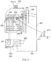
- Figure 1 schematically shows principal components of a generic conventional capacitive touchscreen comprising a physical sensor element 100.
- the touch screen is represented in plan view (to the left in the figure) and also in cross-sectional view (to the right in the figure).
- the touch screen is configured for establishing the position of a touch within a two-dimensional sensing area by providing Cartesian coordinates along an x-direction (horizontal in the figure) and a y-direction (vertical in the figure).
- the sensor element 100 is constructed from a substrate 103 that could be glass or plastic or some other insulating material and upon which is arranged an array of electrodes consisting of multiple laterally extending parallel electrodes, x-electrodes 101, and multiple vertically extending parallel electrodes, y-electrodes 102, which in combination allow the position of a touch 109 to be determined.
- the x-electrodes 101 are aligned parallel to the x-direction and the y-electrodes 102 are aligned parallel to the y-direction.
- the different x-electrodes allow the position of a touch to be determined at different positions along the y-direction while the different y-electrodes allow the position of a touch to be determined at different positions along the x-direction. That is to say in accordance with the terminology used herein, the electrodes are named after their direction of extent rather than the direction along which they resolve position.
- each electrode may have a more detailed structure than the simple "bar" structures represented in Figure 1 , but the operating principles are broadly the same.
- the electrodes which are sometimes called traces, are made of an electrically conductive material such as copper or Indium Tin Oxide (ITO).
- ITO Indium Tin Oxide
- the nature of the various materials used depends on the desired characteristics of the touch screen. For example, a touch screen may need to be transparent, in which case ITO electrodes and a plastic substrate are common.
- a touch pad such as often provided in lieu of a mouse in laptop computers is usually opaque, and hence can use lower cost copper electrodes and an epoxy-glass-fibre substrate (e.g. FR4).
- the electrodes are electrically connected via circuit conductors 104 to a controller chip 105, which is in turn connected to a host processing system 106 by means of a communication interface 107.
- the host 106 interrogates the controller chip 105 to recover the presence and coordinates of any touch or touches present on, or proximate to the sensor 103.
- a front cover also referred to as a lens or panel
- a single touch 109 on the surface of the cover 108 is schematically represented.
- the touch itself does not generally make direct galvanic connection to the sensor 103 or to the electrodes 102. Rather, the touch influences the electric fields 110 that the controller chip 105 generates using the electrodes 102. With appropriate analysis of relative changes in the electrodes' measured capacitance / capacitive coupling, the controller chip 105 can thus calculate a touch position on the cover's surface as an XY coordinate 111. The host system can therefore use the controller chip to detect where a user is touching, and hence take appropriate action, perhaps displaying a menu or activating some function.
- a further aspect of capacitive touch sensors relates to the way the controller chip uses the electrodes of the sensor element to make its measurements.
- controller chip uses the electrodes of the sensor element to make its measurements.
- a first class is known as a "self-capacitance" style.
- the controller 201 will typically apply some electrical stimulus (drive signal) 202 to each electrode 203 which will cause an electric field to form around it 204.
- This field couples through the space around the electrode back to the controller chip via numerous conductive return paths that are part of the nearby circuitry 205, product housing 206, physical elements from the nearby surroundings 207 etc., so completing a capacitive circuit 209.
- the overall sum of return paths is typically referred to as the "free space return path" in an attempt to simplify an otherwise hard-to-visualize electric field distribution.
- the controller is only driving each electrode from a single explicit electrical terminal 208; the other terminal is the capacitive connection via this "free space return path".
- the capacitance measured by the controller is the "self-capacitance" of the electrode (and connected tracks) relative to free space (or Earth as it is sometimes called) i.e. the "self-capacitance” of the electrode.
- Touching or approaching the electrode with a conductive element 210, such as a human finger, causes some of the field to couple via the finger through the connected body 213, through free space and back to the controller.
- This extra return path 211 can be relatively strong for large objects (such as the human body), and so can give a stronger coupling of the electrode's field back to the controller; touching or approaching the electrode hence increases the self-capacitance of the electrode.
- the controller is configured to sense this increase in capacitance.
- the increase is strongly proportional to the area 212 of the applied touch and is normally weakly proportional to the touching body's size (the latter typically offering quite a strong coupling and therefore not being the dominant term in the sum of series connected capacitances).
- the electrodes are arranged on an orthogonal grid, generally with a first set of electrodes on one side of a substantially insulating substrate and the other set of electrodes on the opposite side of the substrate and oriented at nominally 90° to the first set.
- the grid is formed on a single side of the substrate and small conductive bridges are used to allow the two orthogonal sets of electrodes to cross each other without short circuiting.
- One set of electrodes is used to sense touch position in a first axis that we shall call "X" and the second set to sense the touch position in the second orthogonal axis that we shall call "Y".
- the controller can either drive each electrode in turn (sequential) or it can drive them all in parallel.
- any neighbouring electrodes to a driven electrode are sometimes grounded by the controller to prevent them becoming touch sensitive when they are not being sensed (remembering that all nearby capacitive return paths will influence the measured value of the actively driven electrode).
- the nature of the stimulus applied to all the electrodes is typically the same so that the instantaneous voltage on each electrode is approximately the same.
- the drive to each electrode is electrically separate so that the controller can discriminate changes on each electrode individually, but the driving stimulus in terms of voltage or current versus time, is the same. In this way, each electrode has minimal influence on its neighbours (the electrode-to-electrode capacitance is non-zero but its influence is only "felt" by the controller if there is a voltage difference between the electrodes).
- the second class of controller is known as a "mutual-capacitance" style.
- the controller 301 will sequentially stimulate each of an array of transmitter (driven / drive) electrodes 302 that are coupled by virtue of their proximity to an array of receiver electrodes 303.
- the resulting electric field 304 is now directly coupled from the transmitter to each of the nearby receiver electrodes; the "free space” return path discussed above plays a negligible part in the overall coupling back to the controller chip when the sensor is not being touched.
- the area local to and centred on the intersection of a transmitter and a receiver electrode is typically referred to as a "node".
- the electric field 304 is partly diverted to the touching object 305.
- An extra return path to the controller 301 is now established via the body 306 and "free-space" in a similar manner to that described above. However, because this extra return path acts to couple the diverted field directly to the controller chip 301, the amount of field coupled to the nearby receiver electrode 303 decreases. This is measured by the controller chip 301 as a decrease in the "mutual-capacitance" between that particular transmitter electrode and receiver electrodes in the vicinity of the touch. The controller senses this change in capacitance of one or more nodes.
- the magnitude of a capacitance change is nominally proportional to the area 307 of the touch (although the change in capacitance does tend to saturate as the touch area increases beyond a certain size to completely cover the nodes directly under the touch) and weakly proportional to the size of the touching body (for reasons as described above).
- the magnitude of the capacitance change also reduces as the distance between the touch sensor electrodes and the touching object increases.
- the transmitter electrodes and receiver electrodes are arranged as an orthogonal grid, with the transmitter electrodes on one side of a substantially insulating substrate and the receiver electrodes on the opposite side of the substrate.
- This is as schematically shown in Figure 3 .
- a first set of transmitter electrodes 303 is shown on one side of a substantially insulating substrate 308 and a second set of receiver electrodes 302 is arranged at nominally 90° to the transmitter electrodes on the other side of the substrate.
- the grid is formed on a single side of the substrate and small insulating bridges are used to allow the transmitter and receiver electrodes to cross each other without short circuiting.
- a controller chip can typically determine touch positions to a greater resolution than the spacing between electrodes. Also there are established techniques by which multiple touches within a sensing area, and which might be moving, can be uniquely identified and tracked, for example until they leave the sensing area.
- conventional position-sensitive touch sensors are generally configured to provide a position measurements as a Cartesian coordinate within a two-dimensional sensing space which is defined relative to the x-and y-electrodes.
- capacitive sensing controller chips ICs are generally designed to interface to regular linear arrays of straight sensor electrodes, or X and Y electrodes, on a two-dimensional plane.
- a conventional electrode layout coupled to a conventional controller may not be appropriate. This might be, for example, because the design of the touch sensor, and in particular the sensing surface and surrounding connections, is constrained by its application and / or the form of a device into which the sensor is to be incorporated. In particular, in some situations it may be inconvenient or impossible to establish connections from a touch sensor controller chip (IC) to more than one side / edge of a sensing surface. For example, this may be due to a limited availability of space adjacent the sensing area in which to route connections to other edges of the sensing surface. In situations such as this it would be advantageous to employ a sensor having a sensing surface in which connections to the respective electrodes of the sensor may be made along only one of the edges of the sensing surface.
- IC touch sensor controller chip
- US 20110227868 discloses a proximity-sensing panel that includes a substrate panel, one or more proximity-sensing unit and one or more sensing circuit.
- the proximity-sensing unit is formed on the substrate panel.
- the proximity-sensing unit senses motions of an object to generate a proximity-sensing signal accordingly.
- the sensing circuit receives the proximity-sensing signal and generates a control signal to initiate a proximity touch control.
- US 2009/273573 also discloses a proximity-sensing panel wherein the electrodes may be arranged according to a radial coordinates system rather than according to an orthogonal coordinates system.
- a touch-sensitive position sensor in accordance with independent claim 1.
- the processor is configured to transform the reported position to an output position based on a lookup table relating a plurality of possible reported positions to a plurality output positions.
- the processor is configured to transform the reported position to an output position according to a mathematical function associated with the pattern of electrodes.
- the common edge of the sensing surface is a first edge of the sensing surface and the ends of the first electrodes and ends of the second electrodes which meet the first edge of the sensing surface are first ends of respective ones of the first electrodes and first ends of respective ones of the second electrodes, and wherein second ends of the respective ones of the first electrodes meet a second edge of the sensing surface and second ends of the respective ones of the second electrodes meet a third edge of the sensing surface.
- At least one of first electrodes crosses with at least one of the second electrodes but does not cross with at least one other of the first electrodes.
- respective ones of the first electrodes and the second electrodes have a non-uniform width in the plane of the sensing surface which varies in dependence on a distance from the common edge of the sensing surface.
- respective ones of the first electrodes and the second electrodes have a non-uniform width in the plane of the sensing surface which varies in dependence on a distance along the selective electrodes between pairs of nodes.
- respective ones of the first electrodes and / or respective ones of the second electrodes follow generally arcuate paths within the sensing surface.
- the generally arcuate paths within the sensing surface subtend an angle of around 90°.
- the electrical parameter relates to a capacitive coupling associated with the respective electrodes.
- the capacitive coupling is a capacitive coupling between respective ones of the first electrodes and respective ones of the second electrodes.
- the electrical parameter relates to a resistance associated with the electrodes.
- Embodiments of the invention may thus provide a method and apparatus for recovering physical touch positions on a two-layer sensor, e.g. a rectangular sensor, from positions reported by a touch controller in the case where the distances between neighbouring sensor nodes are unequal.
- a two-layer sensor e.g. a rectangular sensor
- a lookup table used to determine the positions of the nearest nodes on the sensor from position reported by the touch controller and further refinement of position is determined by interpolating between these nodes.
- all connections can be made on one edge of the sensor.
- the mathematical relation is chosen to minimise the maximum nearest-neighbour distance of any node (location where electrodes meet or cross) within a sensor.
- the senor has two classification of senor electrodes / lines, which may be referred to D lines (comprising an array of first electrodes) and R lines (comprising an array of second electrodes), and the sensor may comprise uniform width D lines and uniform width R lines with the resulting sensor nodes being formed at the centre of the crossings between each D line and each R line.
- the senor consists of non-uniform width D lines and non-uniform width R lines with the resulting sensor nodes being formed at the centre of the crossings (intersections) between each D line (first electrode) and each R line (second electrode).
- the D lines and R lines are shaped differently in the vicinity of each crossing such that the mutual capacitance between the respective D lines and R lines at the respective intersections between respective ones of the lines are similar.
- Some embodiments of the invention are directed towards addressing this issue by providing sensor electrode patterns that provide a sensing surface for which connections to the electrodes which define the sensing surface can be made along one edge of the active sensing surface (i.e. the surface over which the sensor is able to report positions).
- this can be achieved in accordance with some embodiments of the invention by in effect providing a distorted electrode pattern comprising electrodes that are non-linear within the sensing surface so that electrodes which meet (intersect / cross) one another within the sensing surface nonetheless meet a common edge of the sensing surface.
- the reported position determined with respect to the distorted electrode pattern may be postprocessed to convert it to a physical location, wherein the post-processing takes account of the nature of the distorted electrode pattern (i.e. a transform may be applied to "undo" the effects of the electrode pattern being distorted).
- One coordinate system may be referred to as a "physical" coordinate system and relates to the "real world" position of an object adjacent a sensing surface.
- a physical coordinate system may be used to represent the position of a touch adjacent a two dimensional sensing surface in terms of a number of centimetres away from a reference point along two directions.
- Another coordinate system may be referred to as a "reported" coordinate system and relates to the position of an object adjacent a sensing surface as reported in a coordinate system defined relative to the sensor electrodes.
- a reported coordinate system may be used to represent the position of a touch in terms of which sensor electrodes are in the vicinity of where the touch is detected.
- a controller for a sensor chip will typically output a position in such a "reported” coordinate system (since the controller will naturally calculate positions relative to the electrodes).
- the (interpolated centroid) position of the touch 109 may be defined within a physical coordinate system as being at a position of 2.4 centimetres from the left-hand edge of the sensing area and 3.6 centimetres from the top edge of the sensing area.
- the physical coordinate system is a regular Cartesian coordinate system having an origin at the top left corner of the sensing area and with distance is measured in units of centimetres (of course other origins and units may be used).
- the (interpolated centroid) position of the touch 109 may equally be defined within a reported coordinate system as being around the intersection of the third-from-top x-electrode and the second-from-left y-electrode.
- the reported coordinate system is again a regular Cartesian coordinate system having an origin at the top left corner of the sensing area and with distance is measured in units of electrode separations. It will be appreciated that in general a controller chip will not typically output a reported position that literally uses electrode separations as units, but rather will most likely be configured to output a digitised value for each sensing direction, for example ranging from 0 to 1023 corresponding to the full extent of the sensing area in the relevant direction, wherein the digitised value.
- the physical coordinate system may be seen as defining the location of a touch in "real space” whereas the reported coordinate system may be seen as defining the location of a touch in "controller space” or "reported space”.
- the relationship between the physical (or real-world) coordinate system and the reported (or controller) coordinate system is based around a simple linear scaling of the units use to define position (and a translational offset if different origins are employed).
- a location (x r , y r ) in the controller's reported coordinate system may be transformed into a location (x p , y p ) within the sensing surface's physical coordinate system by simply multiplying x r and y r by a scaling factor based on how physically far apart the respective electrodes are.
- touch sensitive position sensors having electrode patterns which are not arranged on a regular Cartesian grid.
- electrode patterns are provided which comprise an array of first electrodes and an array of second electrodes arranged to provide a sensing surface comprising sensing nodes at locations where respective ones of the first electrodes and the second electrodes meet / intersect / cross, and wherein at least some of the first electrodes and / or the second electrodes are non-linear (i.e. arrange to follow a generally non-linear path, such as a curve) within the sensing area.
- the positions of touches (objects) determined by a conventional sensor controller coupled to the sensor electrode pattern in reported coordinate space differ from the physical positions of the touches relative to the physical sensing surface by more than a simple linear scaling.
- the approach of embodiments of the invention has been found to provide alternative electrode patterns having characteristics which can address some of the issues identified above.
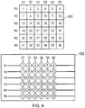
- FIG. 4 schematically shows various aspects of a conventional capacitive touch sensor.
- the capacitive touch sensor is assumed to be based on a mutual-capacitance sensing technique in which a sensing surface 102 is defined by an orthogonal grid of six "receive” electrodes (labelled R1 to R6) and six “drive” electrodes (labelled D1 to D6), as schematically represented in the lower part of Figure 4 .
- These electrodes may be coupled to a conventional touch sensor controller configured to appropriately apply signals to the drive electrodes D1 to D6 and to measure corresponding signals received on the receiver electrodes R1 to R6 in the usual way.
- this type of sensor is primarily sensitive to the location of objects in the vicinity of the respective intersections between the receive electrodes and the drive electrodes.
- the sensing surface may be considered to comprise 36 sensing nodes corresponding to the various intersection / crossing / meeting points as labelled in the figure.
- the presence of an object near to a given sensing node will cause a change in the mutual-capacitance between the respective drive and receiver electrodes in the vicinity of this node.
- a centroid of changes in the mutual-capacitance for a group of sensing nodes may be interpolated to establish a touch position with a precision that is higher than the characteristic electrode spacing.
- FIG. 4 schematically represents the reported position coordinate system for the controller coupled to the sensor.
- the controller is operable to output an indication of the position of an object relative to the locations of the various sensing nodes (i.e. in a coordinate system defined relative to the electrodes).
- the position may be reported.
- x r is a measure of where the object / touch is determined to be relative to the drive electrodes (i.e.
- conventional controllers can "interpolate" positions.
- the relationship between the reported position for an object (x r , y r ) in reported coordinate space and the actual / physical position of an object within the sensing surface in physical space (x p , y p ) is generally a simple linear scaling based around the size of the spacing between electrodes.
- Embodiments of the invention will now be described which are assumed to be based around a mutual-capacitance touch sensor comprising six drive electrodes and six receive electrodes and which may be controlled by a conventional controller such as one which may be used in conjunction with the conventional Cartesian-grid electrode layout shown in Figure 4 .
- a significant aspect of embodiments of the invention is that the electrodes are non-linear within the plane of the sensing surface. Nonetheless, in accordance with embodiments of the invention a sensing surface having non-linear electrodes may be coupled to a broadly conventional-type controller (i.e. a controller that does not "know" the electrodes are not arranged on a conventional regular Cartesian grid).
- FIGS. 5A and 5B schematically represent some aspects of a mutual-capacitance touch sensor according to an embodiment of the invention.
- Figure 5A represents an electrode pattern comprising a first array of six drive electrodes 204 (D1 to D6) and a second array of six receive electrodes 203 (R1 to R6) arranged to cross one another on a physical sensing surface 202 to provide 36 sensing nodes at the respective intersections between respective ones of the drive and receive electrodes.
- the sensor may be manufactured in accordance with any known techniques for providing touch sensor electrodes on a suitable substrate / physical surface.
- the electrode pattern may be formed on a substrate in accordance with known technologies and using conventional materials according to the implementation at hand for (example, whether the sensor is to be transparent or opaque, and so forth).
- Signals applied to and measured from the electrodes D1 to D6 and R1 to R6 may be controlled by a conventional-type touch-sensor controller, such as might be used for driving the conventional touch sensor schematically represented in Figure 4 in order to establish the locations of touches / objects relative to the electrodes in a broadly conventional fashion.
- a controller coupled to the electrodes is arranged to output an estimated position for a touch / object in a reported coordinate space as schematically represented in Figure 5B (i.e. the conventionally-operating controller operates according to an assumption the nodes are arranged on a regular Cartesian grid as is conventional, although in fact they are not).
- the controller is configured to establish where an object is located relative to the drive electrodes and the receive electrodes.
- the locations of objects / touches adjacent the sensing surface represented 202 in Figure 5A may be defined in a physical-space Cartesian coordinate system, which, in this example, is defined by an x-axis running along the top edge of the sensing surface such as schematically represented in Figure 5A and a y-axis running vertically through the centre of the sensing surface.
- a representation of a touch 211 adjacent sensing node 24 is schematically represented as being at physical coordinates (x p , y p ).
- it is the location of a measured touch position in a physical coordinate system which is of primary interest for a device in which the touch sensor is incorporated.
- a controller coupled to the electrodes will initially establish the location of the touch in a reported-space coordinate system defined relative to the electrodes.
- a significant aspect of the electrode pattern in Figure 5A is that the electrodes are not arranged on a regular Cartesian grid, but are non-linear within the plane of the sensing area.
- a result of this arrangement is that a physical location of an object adjacent the sensing area in a physical coordinate system defined relative to the "real world" sensing surface, for example in the physical Cartesian coordinate system (x p , y p ) discussed above, does not linearly map to a reported position in the reported coordinate system (x r , y r ) with fixed scaling.
- respective ones of the drive electrodes D1 to D6 and the receive electrodes R1 to R6 follow generally arcuate paths within the sensing surface defined by the sensing nodes (the sensing surface is the area over which the touch sensor is sensitive to position, and as such is generally bound by the outermost sensing nodes).
- the electrode pattern for the sensing surface evident in Figure 5A is in effect a "distorted" version of a regular Cartesian grid electrode pattern such as represented in Figure 5B .
- a position of a touch in a reported coordinate system may be converted to a position for the touch in a physical coordinate system (x p , y p ) by taking account of the nature of the distortion. This may be achieved based on a mapping between locations in the physical coordinate system and corresponding locations in the reported coordinate system defined relative to the electrodes.
- the mapping may be defined functionally, in which case the conversion from reported coordinates to physical coordinates may be performed mathematically. In other cases the mapping may be defined through a lookup table.
- a reported location in the reported Cartesian coordinate system (x r , y r ) can readily be represented as a location in a reported polar coordinate system ( ⁇ r , r r ).
- the origin of the reported polar coordinate system is in the same place as the origin of the reported-space Cartesian coordinate system discussed above, i.e. in the top-left of the reported coordinate space where the first drive electrode (D1) and the first receive electrode (R1) intersect to define sensing node number 1.
- the line of zero-azimuth for the reported polar coordinate space extends along the x-axis for the reported Cartesian coordinate space, as represented in the figure.
- a physical location in the physical Cartesian coordinate system can readily be represented as a location in a physical polar coordinate system ( ⁇ p , r p ).
- the origin of the physical polar coordinate system is in the same place as the origin of the physical-space Cartesian coordinate system discussed above, i.e. in the middle of the top edge of the sensing surface in the vicinity of sensing node number 1.
- the line of zero-azimuth for the physical polar coordinate space extends rightwards along the x-axis for the physical Cartesian coordinate space, as represented in the figure.
- this distortion broadly corresponds with “fanning out” the reported coordinate system presented in Figure 5B by “twisting” the reported-space y-axis about the origin so that lines corresponding to the orthogonal x- and y-axes in the reported coordinate space are in line with one another in the physical board.
- This fanning out is schematically represented by the heavy arrow marked “DISTORT” in Figure 5B .
- the shapes of the individual electrodes represented in Figure 5A may be determined by simply applying the above-identified distortion (i.e. doubling the azimuth angle for each location) to a regular grid electrode pattern.
- connections to the receive electrodes (R1 to R6) and to the drive electrodes (D1 to D6) can be established along a common edge of the sensing surface, namely the top edge in Figure 5A . Furthermore, these connections may be established within a width which is the same as the widest part of the sensing surface. It will furthermore be appreciated that in accordance with conventional sensing techniques there is no need to establish a connection to the opposite ends of the respective electrodes (i.e. the ends which do not intersect the upper edge of the sensing surface). Accordingly, for the electrode pattern of Figure 5A there is no requirement for a region adjacent the sensing surface through which to route connections such as seen to the left-hand side of the conventional design represented in Figure 3 .
- a conventional controller coupled to a sensor employing the electrode pattern of Figure 5A will detect and report a location (x r , y r ) for the touch 211 in reported coordinate space in accordance with conventional techniques.
- a processor arranged to receive the indication of reported position from a conventional controller in the reported coordinate system can readily transform the reported position to an output position in a physical coordinate system based on the non-linear pattern of electrodes by applying processing in accordance with Equations 3 and 4.
- a physical touch location can be determined for a touch sensor having a sensor electrode pattern to which all external connections can be established along a common edge of the sensing surface within a width that is no wider than the width of the sensing area.
- the active sensing surface is not rectangular (i.e. the sensing nodes do not span a rectangular area). For example, a touch or object in the example region 220 identified in dashed out-line falls outside the sensing area.
- sensing surface which more closely resembles a rectangle. This may be achieved in accordance with embodiments of the invention by providing electrode patterns which correspond to different "distortions" of a regular Cartesian grid.
- Figures 6A and 6B schematically represent aspects of a mutual-capacitance touch sensor according to another embodiment of the invention. These figures are similar to, and will be understood from, the corresponding Figures 5A and 5B and the common aspects of the two sensors will not be described again in detail in the interest of brevity.
- the sensing surface of Figure 6A differs from the sensing surface of Figure 5A by being based on a different mapping between reported coordinates and physical coordinates (i.e. there is a different "distortion" of the regular Cartesian grid assumed by the controller chip coupled to the electrodes). In particular, the distortion is modified so as to provide sensing nodes that span a more rectangular region.
- sensing node 35 in Figure 6A is located further from the vertical central line of the sensing area that the corresponding sensing node in the electrode pattern of Figure 5A , thereby in effect extending the active sensing area to a greater width in the lower part of the sensing surface.
- the electrode pattern of Figure 6A is such that the transform from reported coordinates to physical coordinates is based on a mathematical function - that is to say, the electrode pattern is formulaically defined.
- the separations between neighbouring sensing nodes will generally not be constant.
- the separation between sensing nodes numbered 30 and 36 is significantly larger than the separation between sensing nodes numbered 31 and 25.
- the sensing resolution may be different in different parts of the sensing surface.
- FIG. 7 is similar to, and will be understood from, Figures 5A and 6A and the common aspects of these sensors will not be described again in detail in the interest of brevity.
- the electrode pattern of the sensing surface of Figure 7 is broadly based on the sensing surface of Figure 6A (i.e. based on Equations 5 and 6 above), but is truncated below sensing node 29 to in effect remove that part of the sensing area of Figure 6A which is most restricted in width. This has the advantage of providing a more-rectangular sensing area, but at the cost of losing some sensing ability in that the sensing nodes 30, 35, 36 for the sense of Figure 6A are not available for sensing.
- Electrodes may be arranged to provide sensing nodes at tabulated locations such that a transform from reported positions to physical positions can be established by reference to a corresponding lookup table.
- Such a sensing surface is schematically represented in Figure 8.
- Figure 8 is generally similar to, and will be understood from, Figures 5A , 6A and 7 , and the common aspects of these sensors will not be described again in detail in the interest of brevity.
- the 36 sensing node locations are arranged in a pattern which is generally similar to that of Figure 6A , but in which the sensing nodes are constrained to lie along horizontal straight lines on the physical sensing surface (parallel to the physical coordinate system x-axis). These horizontal lines are evenly spaced in the physical coordinate system and are separated by ⁇ y. Furthermore the sensing nodes lying on each of these horizontal straight lines are equally spaced by an amount ⁇ x. (The sensing nodes on different straight lines are differently spaced because of the different numbers of sensing nodes - i.e. ⁇ x is not the same along each horizontal sensing line).
- a lookup table may thus be defined which specifies the physical coordinates of each sensing node on the physical sensing surface.
- a conventional controller chip will generally report an interpolated position having a resolution greater than the separation between electrodes. Accordingly, it is likely that the exact position reported by controller chip will not correspond exactly with an entry in the lookup table.
- a processor receiving the reported position in a reported coordinate system may be configured to determine the four nearest sensing nodes for a reported "fractional" position. This can readily be determined from the rounded-up and rounded-down values of the two coordinates for the reported position.
- the four nearest sensing nodes are those numbered 28, 29, 34, 35 in the numbering scheme of Figure 6B .
- the processor may then establish the physical locations for these four nearest sensing nodes by reference to the lookup table setting out the physical locations of the sensing nodes (electrode crossing points) and determine an interpolated physical position from the four physical locations of the nearest sensing nodes based on the fractional part of the reported position.
- the electrode patterns can be chosen freely (because they are not constrained to follow any particular mathematical form) and in some cases provide a more uniform response (sensing resolution) over a desired shape sensing area.
- a sensing area of the type represented in Figure 8 can also be truncated in much the same way as a truncated example of the sensing area of Figure 6A is schematically shown in Figure 7 .
- Such a truncated-version of the sensing area of Figure 8 is schematically shown in Figure 9 .
- respective ones of electrodes may have non-uniform widths along their lengths in the plane of the sensing surface. This can be helpful in some cases because touch controllers typically interpolate touch positions by taking into account the signals from several neighbouring electrode nodes. For conventional electrode designs with linear, parallel electrodes, the nodes are regularly spaced at a pitch typically designed to facilitate accurate interpolation for the implementation at hand. In embodiments of the current invention electrode nodes are not generally equally spaced and so the accuracy of interpolation may not be the same in the vicinity of different nodes. If this is considered an issue the shape of the electrodes may be varied from node to node so the range of interpolation accuracies throughout the sensor is improved.
- each electrode might consist of two quasi-parallel wires which vary in their spacing
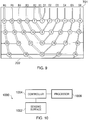
- FIG 10 schematically shows some components of a touch sensor 1000 according to an embodiment of the invention.
- the sensor 1000 comprises a sensing surface 1002, for example in accordance with any of the embodiments of the invention such as discussed above, coupled to a controller chip 1004.
- the controller chip 1004 may, for example, be a conventional "off the shelf' controller chip configured to determine the occurrence of and report a location of a touch using conventional capacitive sensing techniques.
- the sensor 1000 further comprises a processor 1006 arranged to receive a reported position estimate from the controller 1004 and to convert the reported position estimate to a physical position estimate in accordance with the above-describe techniques.
- the processor 1006 may, for example, comprise a suitably programmed general purpose microprocessor, or field programmable gate array, or an application specific integrated circuit.
- the functionality of the controller 1004 and the processor 1006 may be provided in a single element, for example, a single suitablyprogrammed microprocessor.
- embodiments of the invention have primarily focused on touch sensors employing capacitive sensing technologies, and in particular those based on driven and receive electrode based technologies (mutual-capacitance), it will be appreciated that similar considerations apply for sensors employing other capacitive sensing technologies (such as self-capacitance based sensors) or, indeed, touch sensors based on other technologies, such as resistive screen sensors. More generally, embodiments of the invention can be applied to any sensor technology in which sensing is performed by measuring an electrical parameter associated with electrodes.
- embodiments of the invention may in some respects be seen as being based on providing a "distorted" electrode pattern to provide a spatial mapping between a physical touch position and a reported touch position which is nonlinear, and this principle applies regardless of the underlying technology for establishing the reported touch position.
- a touch-sensitive position sensor comprises an array of first electrodes and an array of second electrodes arranged in a pattern to provide a sensing surface, wherein at least some of the first electrodes and the second electrodes are arranged to follow paths which are non-linear within the sensing surface such that there are ends of the first electrodes and ends of the second electrodes which meet a common edge of the sensing surface.
- a controller is coupled to respective ones of the first electrodes and the second electrodes and arranged to determine a reported position for an object adjacent the sensing surface by measuring changes in an electrical parameter e.g. capacitance or resistance, associated with the first electrodes and the second electrodes which is caused by the presence of the object.
- the controller is further operable to provide an indication of the reported position in a first coordinate system defined relative to the first electrodes and the second electrodes
- the sensor further comprises a processor arranged to receive the indication of reported position from the controller in the first coordinate system and to transform the reported position to an output position in a second coordinate system, wherein the transform is based on the non-linear pattern of electrodes.
Claims (12)
- Capteur de position tactile (1000) comprenant :un réseau de premières électrodes (204) et un réseau de secondes électrodes (203) disposés suivant un motif pour fournir une surface de détection (1002), au moins certaines des premières électrodes et des secondes électrodes étant disposées de manière à suivre des chemins non linéaires à l'intérieur de la surface de détection de telle sorte que des extrémités des premières électrodes et des extrémités des secondes électrodes rencontrent un bord linéaire commun de la surface de détection ;un contrôleur (1004) couplé à des électrodes respectives des premières électrodes et des secondes électrodes et conçu de manière à déterminer une position rapportée pour un objet adjacent à la surface de détection en mesurant des changements d'un paramètre électrique associé aux premières électrodes et aux secondes électrodes qui sont causés par la présence de l'objet, et fournir une indication de la position rapportée dans un premier système de coordonnées défini par rapport aux premières électrodes et aux secondes électrodes ;un processeur (1006) conçu pour recevoir l'indication de position rapportée à partir du contrôleur dans le premier système de coordonnées et transformer la position rapportée en une position de sortie dans un second système de coordonnées, la transformation étant basée sur le motif non linéaire des électrodes, etdans lequel la surface de détection couvre une pluralité de nœuds à des emplacements de croisement d'électrodes respectives des premières et secondes électrode, et dans lequel les séparations entre des nœuds adjacents sont différentes pour différents emplacements sur la surface de détection.
- Capteur de position tactile selon la revendication 1, dans lequel le processeur est configuré pour transformer la position rapportée en une position de sortie sur la base d'une table de consultation qui relie une pluralité de positions rapportées possibles à une pluralité de positions de sortie.
- Capteur de position tactile selon n'importe quelle revendication précédente, dans lequel le processeur est configuré pour transformer la position rapportée en une position de sortie selon une fonction mathématique associée au motif d'électrodes.
- Capteur de position tactile selon n'importe quelle revendication précédente, dans lequel le bord commun de la surface de détection est un premier bord de la surface de détection et les extrémités des premières électrodes et extrémités des secondes électrodes qui rencontrent le premier bord de la surface de détection sont des premières extrémités d'électrodes respectives des premières électrodes et des premières extrémités d'électrodes respectives des secondes électrodes, et dans lequel des secondes extrémités d'électrodes respectives des premières électrodes rencontrent un deuxième bord de la surface de détection et des secondes extrémités d'électrodes respectives des secondes électrodes rencontrent un troisième bord de la surface de détection qui est opposé au deuxième bord de la surface de détection.
- Capteur de position tactile selon n'importe quelle revendication précédente, dans lequel au moins certaines des premières électrodes ne se croisent pas avec au moins certaines des secondes électrodes qui se croisent avec d'autres des premières électrodes.
- Capteur de position tactile selon la revendication 1, dans lequel des électrodes respectives des premières électrodes et des secondes électrodes ont une largeur non uniforme dans le plan de la surface de détection qui varie en fonction d'une distance à partir du bord commun de la surface de détection.
- Capteur de position tactile selon la revendication 1, dans lequel des électrodes respectives des premières électrodes et des secondes électrodes ont une largeur non uniforme dans le plan de la surface de détection qui varie en fonction d'une distance le long des électrodes sélectives entre des paires de nœuds.
- Capteur de position tactile selon n'importe quelle revendication précédente, dans lequel des électrodes respectives des premières électrodes et/ou des électrodes respectives des secondes électrodes suivent des trajectoires généralement courbes à l'intérieur de la surface de détection.
- Capteur de position sensible au toucher selon la revendication 9, dans lequel les trajectoires généralement courbes à l'intérieur de la surface de détection ont une étendue d'environ 90°.
- Capteur de position tactile selon n'importe quelle revendication précédente, dans lequel le paramètre électrique se rapporte à un couplage capacitif associé aux électrodes respectives.
- Capteur de position tactile selon la revendication 10, dans lequel le couplage capacitif est un couplage capacitif entre des électrodes respectives des premières électrodes et des électrodes respectives des secondes électrodes.
- Capteur de position tactile selon n'importe quelle revendication précédente, dans lequel le paramètre électrique se rapporte à une résistance associée aux électrodes.
Applications Claiming Priority (2)
| Application Number | Priority Date | Filing Date | Title |
|---|---|---|---|
| GB1217947.9A GB2506675B (en) | 2012-10-08 | 2012-10-08 | Touch sensors and touch sensing methods |
| PCT/GB2013/052615 WO2014057253A1 (fr) | 2012-10-08 | 2013-10-08 | Capteurs tactiles et procédés de détection tactile |
Publications (2)
| Publication Number | Publication Date |
|---|---|
| EP2904479A1 EP2904479A1 (fr) | 2015-08-12 |
| EP2904479B1 true EP2904479B1 (fr) | 2021-11-24 |
Family
ID=47294396
Family Applications (1)
| Application Number | Title | Priority Date | Filing Date |
|---|---|---|---|
| EP13774495.9A Active EP2904479B1 (fr) | 2012-10-08 | 2013-10-08 | Capteurs tactiles et procédés de détection tactile |
Country Status (4)
| Country | Link |
|---|---|
| US (1) | US9588614B2 (fr) |
| EP (1) | EP2904479B1 (fr) |
| GB (1) | GB2506675B (fr) |
| WO (1) | WO2014057253A1 (fr) |
Families Citing this family (7)
| Publication number | Priority date | Publication date | Assignee | Title |
|---|---|---|---|---|
| GB2506676B (en) * | 2012-10-08 | 2015-03-25 | Touchnetix Ltd | Touch sensors and touch sensing methods |
| DE102014211158A1 (de) * | 2014-06-11 | 2015-12-17 | Continental Automotive Gmbh | Tastfeld mit einer verbesserten Berührungserkennung im Randbereich |
| JP6437775B2 (ja) * | 2014-09-30 | 2018-12-12 | エルジー ディスプレイ カンパニー リミテッド | タッチパネル装置およびタッチパネルのタッチ位置座標算出方法 |
| GB2554736B8 (en) * | 2016-10-07 | 2020-02-12 | Touchnetix Ltd | Multi-touch Capacitance Measurements and Displacement Sensing |
| CN107145260B (zh) * | 2017-05-11 | 2020-06-02 | 友达光电(苏州)有限公司 | 触控面板 |
| CN107977124B (zh) * | 2017-11-28 | 2020-11-03 | 友达光电(苏州)有限公司 | 立体触控面板 |
| WO2023250303A1 (fr) * | 2022-06-20 | 2023-12-28 | Microchip Touch Solutions Limited | Capteurs capacitifs de forme irrégulière et emplacements d'événements tactiles au niveau de ceux-ci |
Citations (1)
| Publication number | Priority date | Publication date | Assignee | Title |
|---|---|---|---|---|
| US20090273573A1 (en) * | 2006-07-06 | 2009-11-05 | Apple Inc. | Mutual capacitance touch sensing device |
Family Cites Families (5)
| Publication number | Priority date | Publication date | Assignee | Title |
|---|---|---|---|---|
| US7395717B2 (en) * | 2006-02-10 | 2008-07-08 | Milliken & Company | Flexible capacitive sensor |
| US8654083B2 (en) * | 2006-06-09 | 2014-02-18 | Apple Inc. | Touch screen liquid crystal display |
| TW200901014A (en) | 2007-06-28 | 2009-01-01 | Sense Pad Tech Co Ltd | Touch panel device |
| US8576193B2 (en) * | 2008-04-25 | 2013-11-05 | Apple Inc. | Brick layout and stackup for a touch screen |
| US20110227868A1 (en) * | 2010-03-17 | 2011-09-22 | Edamak Corporation | Proximity-sensing panel |
-
2012
- 2012-10-08 GB GB1217947.9A patent/GB2506675B/en active Active
-
2013
- 2013-10-08 US US14/433,044 patent/US9588614B2/en active Active
- 2013-10-08 EP EP13774495.9A patent/EP2904479B1/fr active Active
- 2013-10-08 WO PCT/GB2013/052615 patent/WO2014057253A1/fr active Application Filing
Patent Citations (1)
| Publication number | Priority date | Publication date | Assignee | Title |
|---|---|---|---|---|
| US20090273573A1 (en) * | 2006-07-06 | 2009-11-05 | Apple Inc. | Mutual capacitance touch sensing device |
Also Published As
| Publication number | Publication date |
|---|---|
| WO2014057253A1 (fr) | 2014-04-17 |
| US9588614B2 (en) | 2017-03-07 |
| GB2506675A (en) | 2014-04-09 |
| EP2904479A1 (fr) | 2015-08-12 |
| US20150234527A1 (en) | 2015-08-20 |
| GB201217947D0 (en) | 2012-11-21 |
| GB2506675B (en) | 2015-08-05 |
Similar Documents
| Publication | Publication Date | Title |
|---|---|---|
| EP2904478B1 (fr) | Capteurs tactiles et procédés de détection tactile | |
| EP2904479B1 (fr) | Capteurs tactiles et procédés de détection tactile | |
| US8552315B2 (en) | Two-dimensional position sensor | |
| US8829926B2 (en) | Transparent proximity sensor | |
| US10558305B2 (en) | Touch sensors | |
| JP5345336B2 (ja) | 入力装置、及びそれを備えた表示装置 | |
| KR101888096B1 (ko) | 접촉 감지 스크린 | |
| US20110048813A1 (en) | Two-dimensional position sensor | |
| US20110310064A1 (en) | User Interfaces and Associated Apparatus and Methods | |
| US20130100041A1 (en) | System for a single-layer sensor having reduced number of interconnect pads for the interconnect periphery of the sensor panel | |
| JP2013501291A (ja) | タッチセンサ | |
| US20140043278A1 (en) | Electrode configuration for large touch screen | |
| TW201533624A (zh) | 觸控面板及其感測方法 | |
| CN106339143B (zh) | 触控基板和触摸屏 | |
| CN102103450B (zh) | 电阻式触控面板 | |
| US11726609B2 (en) | Touch-sensitive apparatus and method | |
| KR101649230B1 (ko) | 터치패널 및 그의 구동방법 | |
| US20130342503A1 (en) | Signal Enhancing Method for Capacitive Touch Panel of Mobile Device | |
| WO2024041967A1 (fr) | Système et procédé tactiles | |
| WO2015118297A1 (fr) | Capteurs tactiles et procédés de détection tactile | |
| CN103455215A (zh) | 具备触控功能的电子装置 |
Legal Events
| Date | Code | Title | Description |
|---|---|---|---|
| PUAI | Public reference made under article 153(3) epc to a published international application that has entered the european phase |
Free format text: ORIGINAL CODE: 0009012 |
|
| 17P | Request for examination filed |
Effective date: 20150324 |
|
| AK | Designated contracting states |
Kind code of ref document: A1 Designated state(s): AL AT BE BG CH CY CZ DE DK EE ES FI FR GB GR HR HU IE IS IT LI LT LU LV MC MK MT NL NO PL PT RO RS SE SI SK SM TR |
|
| AX | Request for extension of the european patent |
Extension state: BA ME |
|
| DAX | Request for extension of the european patent (deleted) | ||
| STAA | Information on the status of an ep patent application or granted ep patent |
Free format text: STATUS: EXAMINATION IS IN PROGRESS |
|
| 17Q | First examination report despatched |
Effective date: 20180614 |
|
| GRAP | Despatch of communication of intention to grant a patent |
Free format text: ORIGINAL CODE: EPIDOSNIGR1 |
|
| STAA | Information on the status of an ep patent application or granted ep patent |
Free format text: STATUS: GRANT OF PATENT IS INTENDED |
|
| INTG | Intention to grant announced |
Effective date: 20201210 |
|
| GRAJ | Information related to disapproval of communication of intention to grant by the applicant or resumption of examination proceedings by the epo deleted |
Free format text: ORIGINAL CODE: EPIDOSDIGR1 |
|
| STAA | Information on the status of an ep patent application or granted ep patent |
Free format text: STATUS: EXAMINATION IS IN PROGRESS |
|
| INTC | Intention to grant announced (deleted) | ||
| GRAP | Despatch of communication of intention to grant a patent |
Free format text: ORIGINAL CODE: EPIDOSNIGR1 |
|
| STAA | Information on the status of an ep patent application or granted ep patent |
Free format text: STATUS: GRANT OF PATENT IS INTENDED |
|
| INTG | Intention to grant announced |
Effective date: 20210618 |
|
| GRAS | Grant fee paid |
Free format text: ORIGINAL CODE: EPIDOSNIGR3 |
|
| GRAA | (expected) grant |
Free format text: ORIGINAL CODE: 0009210 |
|
| STAA | Information on the status of an ep patent application or granted ep patent |
Free format text: STATUS: THE PATENT HAS BEEN GRANTED |
|
| RAP3 | Party data changed (applicant data changed or rights of an application transferred) |
Owner name: TOUCHNETIX LIMITED |
|
| RIN1 | Information on inventor provided before grant (corrected) |
Inventor name: ARD, CHRISTOPHER KYLE Inventor name: SLEEMAN, PETER TIMOTHY Inventor name: ROBERTS, STEPHEN WILLIAM |
|
| AK | Designated contracting states |
Kind code of ref document: B1 Designated state(s): AL AT BE BG CH CY CZ DE DK EE ES FI FR GB GR HR HU IE IS IT LI LT LU LV MC MK MT NL NO PL PT RO RS SE SI SK SM TR |
|
| REG | Reference to a national code |
Ref country code: GB Ref legal event code: FG4D |
|
| REG | Reference to a national code |
Ref country code: DE Ref legal event code: R096 Ref document number: 602013080188 Country of ref document: DE |
|
| REG | Reference to a national code |
Ref country code: AT Ref legal event code: REF Ref document number: 1450355 Country of ref document: AT Kind code of ref document: T Effective date: 20211215 |
|
| REG | Reference to a national code |
Ref country code: IE Ref legal event code: FG4D |
|
| REG | Reference to a national code |
Ref country code: LT Ref legal event code: MG9D |
|
| REG | Reference to a national code |
Ref country code: NL Ref legal event code: MP Effective date: 20211124 |
|
| REG | Reference to a national code |
Ref country code: AT Ref legal event code: MK05 Ref document number: 1450355 Country of ref document: AT Kind code of ref document: T Effective date: 20211124 |
|
| PG25 | Lapsed in a contracting state [announced via postgrant information from national office to epo] |
Ref country code: RS Free format text: LAPSE BECAUSE OF FAILURE TO SUBMIT A TRANSLATION OF THE DESCRIPTION OR TO PAY THE FEE WITHIN THE PRESCRIBED TIME-LIMIT Effective date: 20211124 Ref country code: LT Free format text: LAPSE BECAUSE OF FAILURE TO SUBMIT A TRANSLATION OF THE DESCRIPTION OR TO PAY THE FEE WITHIN THE PRESCRIBED TIME-LIMIT Effective date: 20211124 Ref country code: FI Free format text: LAPSE BECAUSE OF FAILURE TO SUBMIT A TRANSLATION OF THE DESCRIPTION OR TO PAY THE FEE WITHIN THE PRESCRIBED TIME-LIMIT Effective date: 20211124 Ref country code: BG Free format text: LAPSE BECAUSE OF FAILURE TO SUBMIT A TRANSLATION OF THE DESCRIPTION OR TO PAY THE FEE WITHIN THE PRESCRIBED TIME-LIMIT Effective date: 20220224 Ref country code: AT Free format text: LAPSE BECAUSE OF FAILURE TO SUBMIT A TRANSLATION OF THE DESCRIPTION OR TO PAY THE FEE WITHIN THE PRESCRIBED TIME-LIMIT Effective date: 20211124 |
|
| PG25 | Lapsed in a contracting state [announced via postgrant information from national office to epo] |
Ref country code: IS Free format text: LAPSE BECAUSE OF FAILURE TO SUBMIT A TRANSLATION OF THE DESCRIPTION OR TO PAY THE FEE WITHIN THE PRESCRIBED TIME-LIMIT Effective date: 20220324 Ref country code: SE Free format text: LAPSE BECAUSE OF FAILURE TO SUBMIT A TRANSLATION OF THE DESCRIPTION OR TO PAY THE FEE WITHIN THE PRESCRIBED TIME-LIMIT Effective date: 20211124 Ref country code: PT Free format text: LAPSE BECAUSE OF FAILURE TO SUBMIT A TRANSLATION OF THE DESCRIPTION OR TO PAY THE FEE WITHIN THE PRESCRIBED TIME-LIMIT Effective date: 20220324 Ref country code: PL Free format text: LAPSE BECAUSE OF FAILURE TO SUBMIT A TRANSLATION OF THE DESCRIPTION OR TO PAY THE FEE WITHIN THE PRESCRIBED TIME-LIMIT Effective date: 20211124 Ref country code: NO Free format text: LAPSE BECAUSE OF FAILURE TO SUBMIT A TRANSLATION OF THE DESCRIPTION OR TO PAY THE FEE WITHIN THE PRESCRIBED TIME-LIMIT Effective date: 20220224 Ref country code: NL Free format text: LAPSE BECAUSE OF FAILURE TO SUBMIT A TRANSLATION OF THE DESCRIPTION OR TO PAY THE FEE WITHIN THE PRESCRIBED TIME-LIMIT Effective date: 20211124 Ref country code: LV Free format text: LAPSE BECAUSE OF FAILURE TO SUBMIT A TRANSLATION OF THE DESCRIPTION OR TO PAY THE FEE WITHIN THE PRESCRIBED TIME-LIMIT Effective date: 20211124 Ref country code: HR Free format text: LAPSE BECAUSE OF FAILURE TO SUBMIT A TRANSLATION OF THE DESCRIPTION OR TO PAY THE FEE WITHIN THE PRESCRIBED TIME-LIMIT Effective date: 20211124 Ref country code: GR Free format text: LAPSE BECAUSE OF FAILURE TO SUBMIT A TRANSLATION OF THE DESCRIPTION OR TO PAY THE FEE WITHIN THE PRESCRIBED TIME-LIMIT Effective date: 20220225 Ref country code: ES Free format text: LAPSE BECAUSE OF FAILURE TO SUBMIT A TRANSLATION OF THE DESCRIPTION OR TO PAY THE FEE WITHIN THE PRESCRIBED TIME-LIMIT Effective date: 20211124 |
|
| PG25 | Lapsed in a contracting state [announced via postgrant information from national office to epo] |
Ref country code: SM Free format text: LAPSE BECAUSE OF FAILURE TO SUBMIT A TRANSLATION OF THE DESCRIPTION OR TO PAY THE FEE WITHIN THE PRESCRIBED TIME-LIMIT Effective date: 20211124 Ref country code: SK Free format text: LAPSE BECAUSE OF FAILURE TO SUBMIT A TRANSLATION OF THE DESCRIPTION OR TO PAY THE FEE WITHIN THE PRESCRIBED TIME-LIMIT Effective date: 20211124 Ref country code: RO Free format text: LAPSE BECAUSE OF FAILURE TO SUBMIT A TRANSLATION OF THE DESCRIPTION OR TO PAY THE FEE WITHIN THE PRESCRIBED TIME-LIMIT Effective date: 20211124 Ref country code: EE Free format text: LAPSE BECAUSE OF FAILURE TO SUBMIT A TRANSLATION OF THE DESCRIPTION OR TO PAY THE FEE WITHIN THE PRESCRIBED TIME-LIMIT Effective date: 20211124 Ref country code: DK Free format text: LAPSE BECAUSE OF FAILURE TO SUBMIT A TRANSLATION OF THE DESCRIPTION OR TO PAY THE FEE WITHIN THE PRESCRIBED TIME-LIMIT Effective date: 20211124 Ref country code: CZ Free format text: LAPSE BECAUSE OF FAILURE TO SUBMIT A TRANSLATION OF THE DESCRIPTION OR TO PAY THE FEE WITHIN THE PRESCRIBED TIME-LIMIT Effective date: 20211124 |
|
| REG | Reference to a national code |
Ref country code: DE Ref legal event code: R097 Ref document number: 602013080188 Country of ref document: DE |
|
| PLBE | No opposition filed within time limit |
Free format text: ORIGINAL CODE: 0009261 |
|
| STAA | Information on the status of an ep patent application or granted ep patent |
Free format text: STATUS: NO OPPOSITION FILED WITHIN TIME LIMIT |
|
| PG25 | Lapsed in a contracting state [announced via postgrant information from national office to epo] |
Ref country code: AL Free format text: LAPSE BECAUSE OF FAILURE TO SUBMIT A TRANSLATION OF THE DESCRIPTION OR TO PAY THE FEE WITHIN THE PRESCRIBED TIME-LIMIT Effective date: 20211124 |
|
| 26N | No opposition filed |
Effective date: 20220825 |
|
| PG25 | Lapsed in a contracting state [announced via postgrant information from national office to epo] |
Ref country code: SI Free format text: LAPSE BECAUSE OF FAILURE TO SUBMIT A TRANSLATION OF THE DESCRIPTION OR TO PAY THE FEE WITHIN THE PRESCRIBED TIME-LIMIT Effective date: 20211124 |
|
| PG25 | Lapsed in a contracting state [announced via postgrant information from national office to epo] |
Ref country code: MC Free format text: LAPSE BECAUSE OF FAILURE TO SUBMIT A TRANSLATION OF THE DESCRIPTION OR TO PAY THE FEE WITHIN THE PRESCRIBED TIME-LIMIT Effective date: 20211124 Ref country code: IT Free format text: LAPSE BECAUSE OF FAILURE TO SUBMIT A TRANSLATION OF THE DESCRIPTION OR TO PAY THE FEE WITHIN THE PRESCRIBED TIME-LIMIT Effective date: 20211124 |
|
| REG | Reference to a national code |
Ref country code: CH Ref legal event code: PL |
|
| P01 | Opt-out of the competence of the unified patent court (upc) registered |
Effective date: 20230427 |
|
| REG | Reference to a national code |
Ref country code: BE Ref legal event code: MM Effective date: 20221031 |
|
| PG25 | Lapsed in a contracting state [announced via postgrant information from national office to epo] |
Ref country code: LU Free format text: LAPSE BECAUSE OF NON-PAYMENT OF DUE FEES Effective date: 20221008 |
|
| PG25 | Lapsed in a contracting state [announced via postgrant information from national office to epo] |
Ref country code: LI Free format text: LAPSE BECAUSE OF NON-PAYMENT OF DUE FEES Effective date: 20221031 Ref country code: FR Free format text: LAPSE BECAUSE OF NON-PAYMENT OF DUE FEES Effective date: 20221031 Ref country code: CH Free format text: LAPSE BECAUSE OF NON-PAYMENT OF DUE FEES Effective date: 20221031 |
|
| PG25 | Lapsed in a contracting state [announced via postgrant information from national office to epo] |
Ref country code: BE Free format text: LAPSE BECAUSE OF NON-PAYMENT OF DUE FEES Effective date: 20221031 |
|
| PG25 | Lapsed in a contracting state [announced via postgrant information from national office to epo] |
Ref country code: IE Free format text: LAPSE BECAUSE OF NON-PAYMENT OF DUE FEES Effective date: 20221008 |
|
| PGFP | Annual fee paid to national office [announced via postgrant information from national office to epo] |
Ref country code: GB Payment date: 20231018 Year of fee payment: 11 |
|
| PGFP | Annual fee paid to national office [announced via postgrant information from national office to epo] |
Ref country code: DE Payment date: 20231013 Year of fee payment: 11 |
|
| PG25 | Lapsed in a contracting state [announced via postgrant information from national office to epo] |
Ref country code: HU Free format text: LAPSE BECAUSE OF FAILURE TO SUBMIT A TRANSLATION OF THE DESCRIPTION OR TO PAY THE FEE WITHIN THE PRESCRIBED TIME-LIMIT; INVALID AB INITIO Effective date: 20131008 |