EP2902109A1 - Method and device for thermal insulation of micro-reactors - Google Patents
Method and device for thermal insulation of micro-reactors Download PDFInfo
- Publication number
- EP2902109A1 EP2902109A1 EP15154853.4A EP15154853A EP2902109A1 EP 2902109 A1 EP2902109 A1 EP 2902109A1 EP 15154853 A EP15154853 A EP 15154853A EP 2902109 A1 EP2902109 A1 EP 2902109A1
- Authority
- EP
- European Patent Office
- Prior art keywords
- micro
- reactor
- trench
- substrate
- fluidic
- Prior art date
- Legal status (The legal status is an assumption and is not a legal conclusion. Google has not performed a legal analysis and makes no representation as to the accuracy of the status listed.)
- Granted
Links
Images



Classifications
-
- B—PERFORMING OPERATIONS; TRANSPORTING
- B01—PHYSICAL OR CHEMICAL PROCESSES OR APPARATUS IN GENERAL
- B01L—CHEMICAL OR PHYSICAL LABORATORY APPARATUS FOR GENERAL USE
- B01L3/00—Containers or dishes for laboratory use, e.g. laboratory glassware; Droppers
- B01L3/50—Containers for the purpose of retaining a material to be analysed, e.g. test tubes
- B01L3/502—Containers for the purpose of retaining a material to be analysed, e.g. test tubes with fluid transport, e.g. in multi-compartment structures
- B01L3/5027—Containers for the purpose of retaining a material to be analysed, e.g. test tubes with fluid transport, e.g. in multi-compartment structures by integrated microfluidic structures, i.e. dimensions of channels and chambers are such that surface tension forces are important, e.g. lab-on-a-chip
- B01L3/502707—Containers for the purpose of retaining a material to be analysed, e.g. test tubes with fluid transport, e.g. in multi-compartment structures by integrated microfluidic structures, i.e. dimensions of channels and chambers are such that surface tension forces are important, e.g. lab-on-a-chip characterised by the manufacture of the container or its components
-
- B—PERFORMING OPERATIONS; TRANSPORTING
- B01—PHYSICAL OR CHEMICAL PROCESSES OR APPARATUS IN GENERAL
- B01L—CHEMICAL OR PHYSICAL LABORATORY APPARATUS FOR GENERAL USE
- B01L3/00—Containers or dishes for laboratory use, e.g. laboratory glassware; Droppers
- B01L3/50—Containers for the purpose of retaining a material to be analysed, e.g. test tubes
- B01L3/502—Containers for the purpose of retaining a material to be analysed, e.g. test tubes with fluid transport, e.g. in multi-compartment structures
- B01L3/5027—Containers for the purpose of retaining a material to be analysed, e.g. test tubes with fluid transport, e.g. in multi-compartment structures by integrated microfluidic structures, i.e. dimensions of channels and chambers are such that surface tension forces are important, e.g. lab-on-a-chip
- B01L3/502715—Containers for the purpose of retaining a material to be analysed, e.g. test tubes with fluid transport, e.g. in multi-compartment structures by integrated microfluidic structures, i.e. dimensions of channels and chambers are such that surface tension forces are important, e.g. lab-on-a-chip characterised by interfacing components, e.g. fluidic, electrical, optical or mechanical interfaces
-
- B—PERFORMING OPERATIONS; TRANSPORTING
- B01—PHYSICAL OR CHEMICAL PROCESSES OR APPARATUS IN GENERAL
- B01L—CHEMICAL OR PHYSICAL LABORATORY APPARATUS FOR GENERAL USE
- B01L7/00—Heating or cooling apparatus; Heat insulating devices
- B01L7/52—Heating or cooling apparatus; Heat insulating devices with provision for submitting samples to a predetermined sequence of different temperatures, e.g. for treating nucleic acid samples
-
- B—PERFORMING OPERATIONS; TRANSPORTING
- B81—MICROSTRUCTURAL TECHNOLOGY
- B81B—MICROSTRUCTURAL DEVICES OR SYSTEMS, e.g. MICROMECHANICAL DEVICES
- B81B3/00—Devices comprising flexible or deformable elements, e.g. comprising elastic tongues or membranes
- B81B3/0064—Constitution or structural means for improving or controlling the physical properties of a device
- B81B3/0081—Thermal properties
-
- B—PERFORMING OPERATIONS; TRANSPORTING
- B81—MICROSTRUCTURAL TECHNOLOGY
- B81B—MICROSTRUCTURAL DEVICES OR SYSTEMS, e.g. MICROMECHANICAL DEVICES
- B81B7/00—Microstructural systems ; Auxiliary parts of microstructural devices or systems
- B81B7/0083—Temperature control
- B81B7/0087—On-device systems and sensors for controlling, regulating or monitoring
-
- B—PERFORMING OPERATIONS; TRANSPORTING
- B01—PHYSICAL OR CHEMICAL PROCESSES OR APPARATUS IN GENERAL
- B01L—CHEMICAL OR PHYSICAL LABORATORY APPARATUS FOR GENERAL USE
- B01L2200/00—Solutions for specific problems relating to chemical or physical laboratory apparatus
- B01L2200/14—Process control and prevention of errors
- B01L2200/143—Quality control, feedback systems
- B01L2200/147—Employing temperature sensors
-
- B—PERFORMING OPERATIONS; TRANSPORTING
- B01—PHYSICAL OR CHEMICAL PROCESSES OR APPARATUS IN GENERAL
- B01L—CHEMICAL OR PHYSICAL LABORATORY APPARATUS FOR GENERAL USE
- B01L2300/00—Additional constructional details
- B01L2300/08—Geometry, shape and general structure
- B01L2300/0809—Geometry, shape and general structure rectangular shaped
- B01L2300/0816—Cards, e.g. flat sample carriers usually with flow in two horizontal directions
-
- B—PERFORMING OPERATIONS; TRANSPORTING
- B01—PHYSICAL OR CHEMICAL PROCESSES OR APPARATUS IN GENERAL
- B01L—CHEMICAL OR PHYSICAL LABORATORY APPARATUS FOR GENERAL USE
- B01L2300/00—Additional constructional details
- B01L2300/18—Means for temperature control
- B01L2300/1805—Conductive heating, heat from thermostatted solids is conducted to receptacles, e.g. heating plates, blocks
-
- B—PERFORMING OPERATIONS; TRANSPORTING
- B01—PHYSICAL OR CHEMICAL PROCESSES OR APPARATUS IN GENERAL
- B01L—CHEMICAL OR PHYSICAL LABORATORY APPARATUS FOR GENERAL USE
- B01L2300/00—Additional constructional details
- B01L2300/18—Means for temperature control
- B01L2300/1883—Means for temperature control using thermal insulation
-
- B—PERFORMING OPERATIONS; TRANSPORTING
- B81—MICROSTRUCTURAL TECHNOLOGY
- B81B—MICROSTRUCTURAL DEVICES OR SYSTEMS, e.g. MICROMECHANICAL DEVICES
- B81B2201/00—Specific applications of microelectromechanical systems
- B81B2201/05—Microfluidics
- B81B2201/051—Micromixers, microreactors
Definitions
- the present invention relates to thermal properties of micro-structures on a microchip. More in particular, the invention relates to a method of manufacturing thermally insulated micro-reactors on a microchip.
- a micro-reactor also called a micro-structured reactor or a micro-channel reactor, is a device in which chemical reactions take place in a confinement with typical lateral dimensions of a few mm or below.
- Micro-reactors are cavities of microscopic dimensions; they feature systems for controlling their temperature based on heaters and thermometers, which can optionally be integrated within the micro-reactor itself.
- Micro-reactors offer many advantages over conventional scale reactors, including vast improvements in energy efficiency, reaction speed and yield, safety, reliability, scalability, on-site/on-demand production, a much finer degree of process control and reduced consumption of reagents.
- Micro-reactors are fabricated on a plurality of substrates whereby thermally insulating substrates are preferred. In some cases, however, it is necessary to fabricate the micro-reactors together with other fluidic or non-fluidic components, which are preferably fabricated in Si. Silicon, however, is a material with high thermal conductivity. Whether the micro-reactors on-chip are standalone micro-reactors, or whether they are part of an array of micro-reactors, e . g . to analyze a variety of targets in parallel, it is important that increasing temperature in the micro-reactors is not exposed or limited to nearby components or micro-reactors. Apart from the exothermal reactions that take place in the micro-reactor it is desirable that the power to increase temperature in the micro-reactor is minimized.
- the present invention provides a method for manufacturing a micro-fluidic device.
- the method comprises:
- providing at least a partial etch from the semiconductor backside for forming at least one through-substrate trench may comprise completely forming the trench from the backside of the substrate.
- providing at least a partial etch from the semiconductor backside for forming at least one through-substrate trench may comprise partly forming the trench from the front side of the substrate and partly forming the trench from the backside of the substrate.
- first structures are provided in the semiconductor substrate from its front side where the trench is to be provided, and then, after bonding of the cover layer, the remainder of the through-substrate trench is formed from the backside of the semiconductor substrate.
- Providing micro-fluidic channels may comprise providing micro-fluidic channels winded partly or multiple times around the micro-reactor.
- a method according to embodiments of the present invention may further comprise providing means for heating or cooling said micro-reactor.
- providing a through-substrate trench from the semiconductor backside may comprise grinding the semiconductor substrate and performing back side lithography, and patterning and etching said through-substrate trench.
- a Single Nucleotide Polymorphism is a difference in the DNA sequence of one nucleotide only.
- SNP's can result in differences in reactions to drugs and predisposition to illness; thus, cost effective and efficient SNP detection can play an important role in personalized medical care.
- a Lab-on-a-Chip (LoC) system can be used for fast, sensitive and highly specific SNP detection.
- the Lab-on-a-Chip system 299 comprises reaction chambers 300 and other components for performing micro-fluidic actions, such as for example, without being exhaustive, reservoirs 307 for liquids to be inspected, such as e.g.
- a full depth thermal insulation trench 310 is separating the micro-reaction chamber 300 from the other components for thermal conductive purposes.
- thermal insulation of a micro-reaction chamber 300 from the rest of the chip is desired in terms of heating only locations where e.g. PCR has to take place, and not inducing reactions elsewhere or damaging temperature sensitive components like e.g. detectors.
- the micro-reaction chamber 300 is thermally insulated from the rest of the chip, less power is needed to heat the reaction chamber, and the heating time is faster. Disadvantage is that, due to the thermal insulation, cooling time is slower, hence cooling means may need to be provided.
- each micro-reactor 300 may be wrapped by a thermal insulation trench individually.
- a plurality of micro-reactors 300 may be separated from the other components by a common thermal insulation trench.
- On a single chip a combination of both embodiments may be implemented, i.e. at least one micro-reactor 300 may be individually wrapped by a thermal insulation trench 310, while at the same time, at another location on the chip, a plurality of micro-reactors 300 are wrapped by a common thermal insulation trench 310.
- the Lab-on-a-Chip system of FIG. 1 is mainly composed of semiconductor based, e.g.
- silicon based components fabricated on the same chip, but valves, pumps and detectors may be fabricated separately and may be later assembled.
- Silicon is particularly advantageous as a semiconductor substrate material in view of its biocompatibility.
- the use of Si is advantageous as it is material with well-known properties, and the technologies for its processing are well advanced.
- an improved fabrication method of the semiconductor based, e.g. Si based, components is introduced and the characterization of a crucial element of the chip is presented: the micro-reactor where for example DNA amplification may be performed.
- FIG. 1 schematically illustrates a Lab-on-Chip system which may be used for multiple SNP detection.
- Fluid to be inspected e.g. blood, and reagents are loaded in appropriate reservoirs 307, 308; two pumps 306 push them through a mixer 304 into a micro-reactor 300 where DNA amplification (PCR) may take place.
- PCR DNA amplification
- a number, N of fragments of well-defined length and containing the sequences where SNP might be present are amplified.
- the fluid is sent then to a filter 302, for example made of semiconductor, e.g. silicon, pillars having a pre-determined inter-pillar distance of for example 1-2 um.
- the N DNA components are spatially separated, according to the principle of high-performance liquid chromatography, and are routed each to a dedicated detector 301 which detects the presence of SNP.
- heat is dissipated from the micro-reactor 300 where the DNA amplification takes places.
- the heat that is dissipated may affect surrounding components on the micro-chip or may affect other micro-reactors 300 if e.g. an array of micro-reactors is used on the same chip.
- a micro-fluidic device may thermally insulate a micro-reactor, which is a heatable microstructure, from other components on a micro-chip whilst maintaining a mechanical robust construction of the device.
- the invention proposes a technique whereby a through-substrate trench substantially surrounding the micro-reactor, is created. With “substantially surrounding” is meant that the trench covers as much as possible of the circumference of the micro-reactor, e.g. at least 50% thereof, e.g. at least 75% thereof, such as at least 80% thereof or at least 90% thereof. In ideal embodiments, the through-substrate trench would completely surround the micro-reactor.
- the through-substrate trench surrounds the heatable micro-reactor substantially completely, except at that location or those locations where connections are made to the micro-reactor, e.g. by means of the one or more micro-fluidic channels.
- the trench is created at full depth of the semiconductor substrate.
- the proposed invention does not require a carrier wafer for manufacturing the through-substrate trench. Contrary thereto, it provides an anodic bond of the semiconductor substrate, e.g. Si, to a cover layer, e.g. a Pyrex wafer, for sealing micro-fluidic channels prior to providing the full-depth etch of the insulation trench, which is advantageous for mechanical robustness, allows for more complicated thermal insulation trench geometries, and is compatible with automated wafer handling systems typical of mass production tools used in silicon technology.
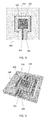
- FIG. 2 illustrates a 3D version of a micro-fluidic device 104
- FIG. 3 illustrates a top view of the same micro-fluidic device 104
- the micro-fluidic device 104 is made in a semiconductor substrate, e.g. a silicon substrate, and comprises a micro-reactor 105 and at least one micro-fluidic channel 101 connected to the micro-reactor 105.
- the micro-reactor 105 comprises a cavity 102, and a semiconductor substrate wall 103, e.g. a silicon wall, forming the micro-reactor 105.
- the micro-fluidic channel 101 is confined by a substrate wall 103.
- a full depth trench 100 i.e.
- a trench completely through the semiconductor substrate surrounds the micro-reactor 105.
- This full depth trench 100 fulfils the purpose of a thermal insulation gap (air).
- the full depth trench 100 ensures that the micro-reactor 105 is not thermally connected to the rest of the micro-chip built on the same substrate and its surrounding components.
- a channel 101 is connected to the cavity 102 of the micro-reactor 105. The channel 101 is separated from the micro-chip and its surrounding components by means of the full depth trench 100.
- the channel 101 can be winded at least partly, i.e. partly, completely or even multiple times, around the micro-reactor 105.
- FIG.4 illustrates a 3D version of a micro-fluidic device 104 with a micro-fluidic channel 101 partially winded around the micro-reactor 105
- FIG. 5 illustrates a top view of the same micro-fluidic device 104.
- the channel 101 is at least partly winded around the micro-reactor 105 to further reduce heat conduction.
- the micro-reactor 105 is separated from the channel 101 by means of a full depth trench 100, i.e. a trench which goes completely through the semiconductor substrate, which fulfills the purpose of a thermal insulation gap.
- the thermal insulation gap is a full depth trench ensuring that the channel 101 and the micro-reactor 105 are not physically, hence not thermally, connected via thermally conductive solid material.
- both the micro-reactor 105 and the at least one micro-fluidic channels 101 are surrounded by a through-substrate trench 100.
- it is a single continuous trench 100 which surrounds both the micro-reactor 105 and the at micro-fluidic channel 101.
- FIG. 6 and FIG. 7 illustrate a top view and a cross-sectional view, respectively, of the schematic of a thermal insulation solution for a micro-fluidic device 104 where two micro-fluidic channels 101 are connected to a micro-reactor 105. Each of the channels 101 is partly winded around the micro-reactor 105. The micro-reactor is attached to two channels 101 for transporting liquid to and from the micro-reactor 105. In the embodiment illustrated, the channels 101 are each partly winded around the micro-reactor to reduce further heat conduction.
- FIG. 7 illustrates a sectional view of a micro-reactor 105 whereby 2 channels 101 are connected to the micro-reactor 105.
- the micro-reactor 105 and the 2 channels 101 are insulated from each other and from other surrounding components on the micro-chip by means of a full depth trench 100.
- the micro-fluidic components such as the micro-fluidic channels 101 and the cavity 102 are sealed by a top cover 106, for example a Pyrex cover or a Schott glass 33 cover, or a cover of another material, e.g. glass, suited for anodic bonding. Pyrex is particularly advantageous as material forming the top cover, in view of its biocompatibility.
- FIG. 6 illustrates a top view of the thermally insulated micro-reactor 105. From the figure it is clear that the channels 101 are each partly winded around the micro-reactor 105, i.e. the channels 101 do not describe the complete circumference of the micro-reactor 105.
- the micro-reactor 105 is connected to one or more channels which are insulated from each other by means of a full depth trench 100 and are fully or even multiple times winded around the micro-reactor 105.
- a plurality of micro-reactors 300 are located on the same micro-chip whereby the micro-reactors 300 and their connected micro-fluidic channels 101 are separated from one another other via a full depth etch insulation trench 310. It is an advantage of this embodiment that the thermal insulation provided by the full-depth trench reduces the thermal mass of the insulated devices and hence allows rapid heating rates and allows individual micro-reactors to be controlled to pre-set thermocycling conditions, independent of neighboring reaction cavities when an array format is used. The capability of loosing heat, hence cooling, is reduced, but this can be solved by adding an additional cooling component.
- a plurality of micro-reactors 300 may be clustered together inside a single insulation trench 310, thus providing thermal insulation between the plurality of micro-reactors 300 and the remainder of the chip. It is an advantage of this embodiments that the thermal insulation provided by the full-depth trench allows heating and/or cooling of the plurality of micro-reactors 300 without at the same time substantially changing the temperature of other micro-fluidic components present in the surrounding substrate.
- the micro-reactor 105, 300 further comprises a means for heating and/or cooling the micro-reactor.
- the means for heating and/or cooling the micro-reactor 105, 300 may be provided at the bottom of the cavity 102.
- the means for heating and/or cooling may be protected from biological material by a layer of protection material, for example a thin layer of silicon nitride.
- the means for heating may be a micro-heater, for example a platinum micro-heater.
- the heater may be provided in the form of a resistor.
- the means for cooling may be a thermoelectric cooler.
- a temperature control system can be used to control individual heating or cooling means of the micro-reactors.
- the temperature control system delivers a variable power to the micro-reactor cavity depending on target and actual cavity temperatures. It may also control the current in the thermoelectric cooler to provide cooling when needed.
- FIG. 8 illustrates a 3D view of the micro-fluidic device 104 illustrated in top view in FIG. 6 and in cross-section in FIG. 7 .
- the present invention provides a method for manufacturing a device comprising at least one thermally insulated micro-reactor 105 and one or more micro-fluidic channels 101.
- the fabrication comprises three major parts:
- FIG. 9 illustrates a schematic of a first embodiment of a process flow according to the present invention:
- FIG. 10 illustrates a schematic of a second embodiment of a process flow according to the present invention:
- the anodic bonding between the semiconductor substrate 900 and the cover wafer 903 is performed before completely providing the through-substrate trenches 100 - hence either before etching of the through-substrate trenches 100 is started, or after a partial etch of the through-substrate trenches 100.
- this increases the mechanical strength hence the robustness of the device, it also allows using standard handling equipment: if full holes are provided through the semiconductor substrate, clamping to vacuum chucks becomes impossible and the use of robot arms for wafer loading/unloading can easily cause wafer break.
- sample inlet and outlet openings 107 may be provided, e.g. etched, through the semiconductor substrate. This is not shown in the process flows, but such inlet and outlet openings 107 are illustrated in FIG. 6 .
- the micro-reactor 105 consists of a 3 ⁇ l cavity 102 about 300 ⁇ m deep.
- High thermal insulation of the reaction chamber from the remaining of the chip is obviously of paramount importance, but in the art difficult to realize, because of the high thermal conductivity of semiconductor substrate material, e.g. silicon.
- the problem has been solved by providing a through-substrate insulation trench 100 around the micro-reactor 105. This etch step for making the insulation trench 100 may at the same time be exploited for opening micro-fluidic ports to the micro-fluidic channels 101.
- the etch of the trench 100 is performed at least partially after anodic bonding, it is possible to completely eliminate semiconductor material, e.g. silicon, from the trench 100.
- Thermal insulation has been further augmented by using long, thermally insulated micro-channels 101 for the inlet and outlet to the micro-reactor 105.
- the micro-channels 101 are winded around the micro-reactor 105.
- the effectiveness of the design is confirmed by experimental results: when the temperature of the micro-reactors 105 is close to 100 °C the temperature of the surrounding part of the chip is only a few degrees above the ambient.
- the thermal mass of that piece of semiconductor substrate comprising the micro-reactors 105 which is actually heated is reduced (thanks to the trench 100 substantially only the micro-reactor 105 is heated, and substantially no surrounding substrate), which allows fast temperature cycling.
- an appropriate temperature control system is utilized in combination with each of the plurality of micro-reactors 105.
- an advanced thermal solution is developed and experimental heating times of less than 1.5 sec from 68 °C to 98 °C and cooling times of less than 2.5 sec from 98 °C to 57 °C (see FIG. 11 ) are demonstrated. It can be seen from this graph that in accordance with embodiments of the present invention fast micro reactor temperature cycling is possible after careful optimization of the various components of the thermal solution.
- FIG.12 illustrates experimental results of the thermal insulation solution in accordance with embodiments of the present invention. It should be noticed that while the temperature of the micro-reactor (PCR) is increasing, the increase of the temperature of the micro-chip (silicon chip) is not proportional to the increase of the temperature of the micro-reactor. This proves that the thermal insulation gap by means of a full depth trench is good solution.
- PCR micro-reactor
- micro-chip silicon chip
Landscapes
- Chemical & Material Sciences (AREA)
- Health & Medical Sciences (AREA)
- Clinical Laboratory Science (AREA)
- Chemical Kinetics & Catalysis (AREA)
- General Health & Medical Sciences (AREA)
- Engineering & Computer Science (AREA)
- Hematology (AREA)
- Analytical Chemistry (AREA)
- Dispersion Chemistry (AREA)
- Computer Hardware Design (AREA)
- Microelectronics & Electronic Packaging (AREA)
- Life Sciences & Earth Sciences (AREA)
- Biochemistry (AREA)
- Molecular Biology (AREA)
- Physics & Mathematics (AREA)
- Thermal Sciences (AREA)
- Micromachines (AREA)
- Physical Or Chemical Processes And Apparatus (AREA)
Abstract
- providing a semiconductor substrate (900) having a front side and a back side;
- providing at least one micro-reactor (105) in said semiconductor substrate (900);
- providing one or more micro-fluidic channels (101) in the front side of said semiconductor substrate (900), connected to said at least one micro-reactor (105);
- sealing said micro-fluidic channels (101) by bonding of a cover layer (903) to the front side of the semiconductor substrate (900); and
- thereafter, from the semiconductor backside, providing at least a partial etch for forming at least one through-substrate trench (100) surrounding said at least one micro-reactor (105) and the one or more micro-fluidic channels (101).
Description
- The present invention relates to thermal properties of micro-structures on a microchip. More in particular, the invention relates to a method of manufacturing thermally insulated micro-reactors on a microchip.
- A micro-reactor, also called a micro-structured reactor or a micro-channel reactor, is a device in which chemical reactions take place in a confinement with typical lateral dimensions of a few mm or below. Micro-reactors are cavities of microscopic dimensions; they feature systems for controlling their temperature based on heaters and thermometers, which can optionally be integrated within the micro-reactor itself. Micro-reactors offer many advantages over conventional scale reactors, including vast improvements in energy efficiency, reaction speed and yield, safety, reliability, scalability, on-site/on-demand production, a much finer degree of process control and reduced consumption of reagents.
- Micro-reactors are fabricated on a plurality of substrates whereby thermally insulating substrates are preferred. In some cases, however, it is necessary to fabricate the micro-reactors together with other fluidic or non-fluidic components, which are preferably fabricated in Si. Silicon, however, is a material with high thermal conductivity. Whether the micro-reactors on-chip are standalone micro-reactors, or whether they are part of an array of micro-reactors, e.g. to analyze a variety of targets in parallel, it is important that increasing temperature in the micro-reactors is not exposed or limited to nearby components or micro-reactors. Apart from the exothermal reactions that take place in the micro-reactor it is desirable that the power to increase temperature in the micro-reactor is minimized.
- It can be concluded that thermal insulation of the micro-reactor is necessary in order to minimize the power necessary for increasing its temperature and to avoid heating of nearby components.
- In "Single step cell lysis/PCR detection of Escherichia coli in an independently controllable silicon microreactor", Sensors and Actuators B 120 (2007) pp.538-544, Cathy Ke et al. describe a micro-reactor designed and modeled to examine thermal properties such as temperature uniformity, power consumption, heating and cooling rates. The micro-reactor contains an etched thermal isolation channel around the reaction cavity, which provides insulation from the surrounding silicon substrate. This channel improves the thermal performance. The depth of the reaction cavity is equal to the depth of the etched thermal isolation channel causing thermal properties of the micro-reactor to be inadequate, in view of parasitic heat dissipation through the substrate.
- In "Boiling heat transfer in rectangular microchannels with reentrant cavities", International Journal of Heat and Mass Transfer 48 (2005) pp.4867-4886, Ali Kozar et al. describe conducted boiling heat transfer experiments in flow through microchannels with reentrant cavities. Insulation cavities are etched in a silicon substrate adjacent to an array of microfluidic channels. The insulation trenches are etched the full depth of the wafer prior to anodic bonding. The fabrication procedure is not practical for insulating micro-reactors since the thermal insulation trench leaves the micro-reactor weakly supported.
- In "Measurements and Modeling of Two-Phase Flow in Microchannels With Nearly Constant Heat Flux Boundary Conditions", Journal of Microelectromechanical Systems, Vol. 11, No. 1, February 2002, Zhang et al. describe a 2 cm long beam attached to silicon plates on both ends for thermal insulation. The full-depth thermal insulation etch is performed after mounting the wafer to a support wafer with photoresist, thus requiring supplementary steps. The device chip comprising the beam is then anodically bonded to Pyrex. For this anodic bonding, the support wafer should be removed to avoid carbonization of the resist or degradation of any other type of adhesive which could be used. It is a disadvantage that the method to fabricate the device as described faces the problem of handling a perforated wafer. Furthermore, the method described does not allow complicated insulation trench geometries without jeopardizing the mechanical robustness of the device.
- It can be concluded that there is a clear need for thermally insulated devices on microchips, such as micro-reactors.
- It is an object of embodiments of the present invention to provide a method of manufacturing thermally insulated devices, such as micro-reactors, on microchips.
- The above objective is accomplished by a method according to the present invention.
- In one aspect, the present invention provides a method for manufacturing a micro-fluidic device. The method comprises:
- providing a semiconductor substrate, e.g. a silicon substrate, having a front side and a back side;
- providing at least one micro-reactor in said semiconductor substrate;
- providing one or more micro-fluidic channels in the front side of said semiconductor substrate, connected to said at least one micro-reactor;
- sealing said micro-fluidic channels by bonding of a cover layer, e.g. anodic bonding of a Pyrex layer, to the front side of the semiconductor substrate; and
- thereafter, from the semiconductor backside, providing at least a partial etch for forming at least one through-substrate trench substantially completely surrounding said at least one micro-reactor and the one or more micro-fluidic channels.
- By providing the through-substrate trenches only after sealing the micro-fluidic channels by a cover layer, the mechanical robustness of the device to be handled during further processing is increased, hence it becomes possible to handle such device with standard automated machines.
- In embodiments of the present invention, providing at least a partial etch from the semiconductor backside for forming at least one through-substrate trench may comprise completely forming the trench from the backside of the substrate. In alternative embodiments, providing at least a partial etch from the semiconductor backside for forming at least one through-substrate trench may comprise partly forming the trench from the front side of the substrate and partly forming the trench from the backside of the substrate. In this embodiment, first structures are provided in the semiconductor substrate from its front side where the trench is to be provided, and then, after bonding of the cover layer, the remainder of the through-substrate trench is formed from the backside of the semiconductor substrate.
- Providing micro-fluidic channels may comprise providing micro-fluidic channels winded partly or multiple times around the micro-reactor.
- A method according to embodiments of the present invention may further comprise providing means for heating or cooling said micro-reactor.
- In a method according to embodiments of the present invention, providing a through-substrate trench from the semiconductor backside may comprise grinding the semiconductor substrate and performing back side lithography, and patterning and etching said through-substrate trench.
- It is an advantage of embodiments of the present invention that heat dissipation towards other components on the micro-chip from these thermally insulated micro-reactors is minimized while a sufficient degree of robustness of the device is maintained.
- Particular and preferred aspects of the invention are set out in the accompanying independent and dependent claims. Features from the dependent claims may be combined with features of the independent claims and with features of other dependent claims as appropriate and not merely as explicitly set out in the claims.
- For purposes of summarizing the invention and the advantages achieved over the prior art, certain objects and advantages of the invention have been described herein above. Of course, it is to be understood that not necessarily all such objects or advantages may be achieved in accordance with any particular embodiment of the invention. Thus, for example, those skilled in the art will recognize that the invention may be embodied or carried out in a manner that achieves or optimizes one advantage or group of advantages as taught herein without necessarily achieving other objects or advantages as may be taught or suggested herein.
- The above and other aspects of the invention will be apparent from and elucidated with reference to the embodiment(s) described hereinafter.
- The invention will now be described further, by way of example, with reference to the accompanying drawings, in which:
-
FIG. 1 illustrates A lab-on-chip implementation for DNA amplification -
FIG. 2 illustrates a 3D view of a micro-fluidic device. -
FIG. 3 illustrates a top view of the micro-fluidic device ofFIG. 2 . -
FIG. 4 illustrates a 3D view of a micro-fluidic device. -
FIG. 5 illustrates a top view of the micro-fluidic device ofFIG. 4 . -
FIG. 6 illustrates a top view,FIG. 7 a cross-sectional view andFIG. 8 a 3D view of a micro-fluidic device. -
FIG. 9 illustrates different processing steps to create thermal insulation structures according to a first method embodiment of the present invention. -
FIG. 10 illustrates different processing steps to create thermal insulation structures according to a second method embodiment of the present invention. -
FIG. 11 illustrates a graph of temperature changes in a micro-reactor insulated in accordance with embodiments of the present invention. -
FIG. 12 : illustrates temperature differences in a micro-reactor and a micro-chip according to embodiments of the present invention. - The drawings are only schematic and are non-limiting. In the drawings, the size of some of the elements may be exaggerated and not drawn on scale for illustrative purposes. The dimensions and the relative dimensions do not necessarily correspond to actual reductions to practice of the invention.
- Any reference signs in the claims shall not be construed as limiting the scope.
- In the different drawings, the same reference signs refer to the same or analogous elements.
- The present invention will be described with respect to particular embodiments and with reference to certain drawings but the invention is not limited thereto but only by the claims.
- The terms first, second and the like in the description and in the claims are used for distinguishing between similar elements and not necessarily for describing a sequence, either temporally, spatially, in ranking or in any other manner. It is to be understood that the terms so used are interchangeable under appropriate circumstances and that the embodiments of the invention described herein are capable of operation in other sequences than described or illustrated herein.
- Moreover, the terms top, under and the like in the description and the claims are used for descriptive purposes and not necessarily for describing relative positions. It is to be understood that the terms so used are interchangeable under appropriate circumstances and that the embodiments of the invention described herein are capable of operation in other orientations than described or illustrated herein.
- It is to be noticed that the term "comprising", used in the claims, should not be interpreted as being restricted to the means listed thereafter; it does not exclude other elements or steps. It is thus to be interpreted as specifying the presence of the stated features, integers, steps or components as referred to, but does not preclude the presence or addition of one or more other features, integers, steps or components, or groups thereof. Thus, the scope of the expression "a device comprising means A and B" should not be limited to devices consisting only of components A and B. It means that with respect to the present invention, the only relevant components of the device are A and B.
- Reference throughout this specification to "one embodiment" or "an embodiment" means that a particular feature, structure or characteristic described in connection with the embodiment is included in at least one embodiment of the present invention. Thus, appearances of the phrases "in one embodiment" or "in an embodiment" in various places throughout this specification are not necessarily all referring to the same embodiment, but may. Furthermore, the particular features, structures or characteristics may be combined in any suitable manner, as would be apparent to one of ordinary skill in the art from this disclosure, in one or more embodiments.
- Similarly it should be appreciated that in the description of exemplary embodiments of the invention, various features of the invention are sometimes grouped together in a single embodiment, figure, or description thereof for the purpose of streamlining the disclosure and aiding in the understanding of one or more of the various inventive aspects. This method of disclosure, however, is not to be interpreted as reflecting an intention that the claimed invention requires more features than are expressly recited in each claim. Rather, as the following claims reflect, inventive aspects lie in less than all features of a single foregoing disclosed embodiment. Thus, the claims following the detailed description are hereby expressly incorporated into this detailed description, with each claim standing on its own as a separate embodiment of this invention.
- Furthermore, while some embodiments described herein include some but not other features included in other embodiments, combinations of features of different embodiments are meant to be within the scope of the invention, and form different embodiments, as would be understood by those in the art. For example, in the following claims, any of the claimed embodiments can be used in any combination.
- It should be noted that the use of particular terminology when describing certain features or aspects of the invention should not be taken to imply that the terminology is being re-defined herein to be restricted to include any specific characteristics of the features or aspects of the invention with which that terminology is associated.
- In the description provided herein, numerous specific details are set forth. However, it is understood that embodiments of the invention may be practiced without these specific details. In other instances, well-known methods, structures and techniques have not been shown in detail in order not to obscure an understanding of this description.
- A Single Nucleotide Polymorphism (SNP) is a difference in the DNA sequence of one nucleotide only. In humans, SNP's can result in differences in reactions to drugs and predisposition to illness; thus, cost effective and efficient SNP detection can play an important role in personalized medical care. For fast, sensitive and highly specific SNP detection a Lab-on-a-Chip (LoC) system can be used. A representative example of such a Lab-on-
a-Chip system 299 and of its functionality is given inFIG. 1 . The Lab-on-a-Chip system 299 comprisesreaction chambers 300 and other components for performing micro-fluidic actions, such as for example, without being exhaustive,reservoirs 307 for liquids to be inspected, such as e.g. blood,reservoirs 308 for reagents,reservoirs 309 for waste, pumps 306 for pumping liquids fromreservoirs mixer 304 for mixing e.g. liquids to be inspected and reagents,valves 305 at different places in the micro-fluidic system, amobile phase 303 andseparation column 302 which together form a simple system for on chip high performance liquid chromatography,detectors 301 for detecting features of the liquid to be inspected. As can be seen inFIG. 1 , according to embodiments of the present invention, a full depththermal insulation trench 310 is separating themicro-reaction chamber 300 from the other components for thermal conductive purposes. This is because thermal insulation of amicro-reaction chamber 300 from the rest of the chip is desired in terms of heating only locations where e.g. PCR has to take place, and not inducing reactions elsewhere or damaging temperature sensitive components like e.g. detectors. On the other hand, if themicro-reaction chamber 300 is thermally insulated from the rest of the chip, less power is needed to heat the reaction chamber, and the heating time is faster. Disadvantage is that, due to the thermal insulation, cooling time is slower, hence cooling means may need to be provided. - As illustrated in the top part of
FIG. 1 , each micro-reactor 300 may be wrapped by a thermal insulation trench individually. Alternatively, as illustrated in the bottom part ofFIG. 1 , a plurality ofmicro-reactors 300 may be separated from the other components by a common thermal insulation trench. On a single chip, a combination of both embodiments may be implemented, i.e. at least one micro-reactor 300 may be individually wrapped by athermal insulation trench 310, while at the same time, at another location on the chip, a plurality ofmicro-reactors 300 are wrapped by a commonthermal insulation trench 310. The Lab-on-a-Chip system ofFIG. 1 is mainly composed of semiconductor based, e.g. silicon based, components fabricated on the same chip, but valves, pumps and detectors may be fabricated separately and may be later assembled. Silicon is particularly advantageous as a semiconductor substrate material in view of its biocompatibility. Furthermore, the use of Si is advantageous as it is material with well-known properties, and the technologies for its processing are well advanced. In embodiments of the present invention an improved fabrication method of the semiconductor based, e.g. Si based, components is introduced and the characterization of a crucial element of the chip is presented: the micro-reactor where for example DNA amplification may be performed. -
FIG. 1 schematically illustrates a Lab-on-Chip system which may be used for multiple SNP detection. Fluid to be inspected, e.g. blood, and reagents are loaded inappropriate reservoirs pumps 306 push them through amixer 304 into a micro-reactor 300 where DNA amplification (PCR) may take place. As an example, a number, N, of fragments of well-defined length and containing the sequences where SNP might be present are amplified. The fluid is sent then to afilter 302, for example made of semiconductor, e.g. silicon, pillars having a pre-determined inter-pillar distance of for example 1-2 um. Here, the N DNA components are spatially separated, according to the principle of high-performance liquid chromatography, and are routed each to adedicated detector 301 which detects the presence of SNP. - It is an object of embodiments of the present invention to reduce heat dissipation from
micro-reactors 300 to surrounding components on a micro-chip. - In the lab-on-chip implementation illustrated in
FIG. 1 , heat is dissipated from the micro-reactor 300 where the DNA amplification takes places. The heat that is dissipated may affect surrounding components on the micro-chip or may affectother micro-reactors 300 if e.g. an array of micro-reactors is used on the same chip. - A micro-fluidic device may thermally insulate a micro-reactor, which is a heatable microstructure, from other components on a micro-chip whilst maintaining a mechanical robust construction of the device. The invention proposes a technique whereby a through-substrate trench substantially surrounding the micro-reactor, is created. With "substantially surrounding" is meant that the trench covers as much as possible of the circumference of the micro-reactor, e.g. at least 50% thereof, e.g. at least 75% thereof, such as at least 80% thereof or at least 90% thereof. In ideal embodiments, the through-substrate trench would completely surround the micro-reactor. This, however, is not possible if an access to the micro-reactor needs to be provided, such as for example with a micro-reactor, where a micro-fluidic channel is connected to that micro-reactor for delivering fluids thereto or for evacuating fluids therefrom. In such cases, the through-substrate trench surrounds the heatable micro-reactor substantially completely, except at that location or those locations where connections are made to the micro-reactor, e.g. by means of the one or more micro-fluidic channels.
- To optimize the thermal insulation properties of the micro-reactor, in accordance with embodiments of the present invention the trench is created at full depth of the semiconductor substrate. The proposed invention does not require a carrier wafer for manufacturing the through-substrate trench. Contrary thereto, it provides an anodic bond of the semiconductor substrate, e.g. Si, to a cover layer, e.g. a Pyrex wafer, for sealing micro-fluidic channels prior to providing the full-depth etch of the insulation trench, which is advantageous for mechanical robustness, allows for more complicated thermal insulation trench geometries, and is compatible with automated wafer handling systems typical of mass production tools used in silicon technology.
-
FIG. 2 illustrates a 3D version of amicro-fluidic device 104, andFIG. 3 illustrates a top view of the samemicro-fluidic device 104. Themicro-fluidic device 104 is made in a semiconductor substrate, e.g. a silicon substrate, and comprises a micro-reactor 105 and at least onemicro-fluidic channel 101 connected to the micro-reactor 105. The micro-reactor 105 comprises acavity 102, and asemiconductor substrate wall 103, e.g. a silicon wall, forming the micro-reactor 105. Also themicro-fluidic channel 101 is confined by asubstrate wall 103. Afull depth trench 100, i.e. a trench completely through the semiconductor substrate, surrounds the micro-reactor 105. Thisfull depth trench 100 fulfils the purpose of a thermal insulation gap (air). Thefull depth trench 100 ensures that the micro-reactor 105 is not thermally connected to the rest of the micro-chip built on the same substrate and its surrounding components. To transport liquid to and from the micro-reactor 105, achannel 101 is connected to thecavity 102 of the micro-reactor 105. Thechannel 101 is separated from the micro-chip and its surrounding components by means of thefull depth trench 100. - It is an object of embodiments of the present invention to still further reduce heat conduction of the micro-reactor 105. To further reduce heat conduction, in accordance with embodiments of the present invention, the
channel 101 can be winded at least partly, i.e. partly, completely or even multiple times, around the micro-reactor 105. -
FIG.4 illustrates a 3D version of amicro-fluidic device 104 with amicro-fluidic channel 101 partially winded around the micro-reactor 105, andFIG. 5 illustrates a top view of the samemicro-fluidic device 104. In such embodiments, thechannel 101 is at least partly winded around the micro-reactor 105 to further reduce heat conduction. The micro-reactor 105 is separated from thechannel 101 by means of afull depth trench 100, i.e. a trench which goes completely through the semiconductor substrate, which fulfills the purpose of a thermal insulation gap. The thermal insulation gap is a full depth trench ensuring that thechannel 101 and the micro-reactor 105 are not physically, hence not thermally, connected via thermally conductive solid material. Also thechannel 101 is separated from other components of the micro-chip by means of afull depth trench 100, which also fulfills the purpose of a thermal insulation gap. Hence, in accordance with embodiments of the present invention, both the micro-reactor 105 and the at least onemicro-fluidic channels 101 are surrounded by a through-substrate trench 100. In the embodiment illustrated inFIG. 4 andFIG. 5 , it is a singlecontinuous trench 100 which surrounds both the micro-reactor 105 and the atmicro-fluidic channel 101. -
FIG. 6 andFIG. 7 illustrate a top view and a cross-sectional view, respectively, of the schematic of a thermal insulation solution for amicro-fluidic device 104 where twomicro-fluidic channels 101 are connected to a micro-reactor 105. Each of thechannels 101 is partly winded around the micro-reactor 105. The micro-reactor is attached to twochannels 101 for transporting liquid to and from the micro-reactor 105. In the embodiment illustrated, thechannels 101 are each partly winded around the micro-reactor to reduce further heat conduction. -
FIG. 7 illustrates a sectional view of a micro-reactor 105 whereby 2channels 101 are connected to the micro-reactor 105. The micro-reactor 105 and the 2channels 101 are insulated from each other and from other surrounding components on the micro-chip by means of afull depth trench 100. The micro-fluidic components such as themicro-fluidic channels 101 and thecavity 102 are sealed by atop cover 106, for example a Pyrex cover or a Schott glass 33 cover, or a cover of another material, e.g. glass, suited for anodic bonding. Pyrex is particularly advantageous as material forming the top cover, in view of its biocompatibility.FIG. 6 illustrates a top view of the thermally insulatedmicro-reactor 105. From the figure it is clear that thechannels 101 are each partly winded around the micro-reactor 105, i.e. thechannels 101 do not describe the complete circumference of the micro-reactor 105. - In embodiments, not illustrated in the drawings, the micro-reactor 105 is connected to one or more channels which are insulated from each other by means of a
full depth trench 100 and are fully or even multiple times winded around the micro-reactor 105. - In particular embodiments, as for example illustrated in
FIG. 1 , a plurality ofmicro-reactors 300 are located on the same micro-chip whereby the micro-reactors 300 and their connectedmicro-fluidic channels 101 are separated from one another other via a full depthetch insulation trench 310. It is an advantage of this embodiment that the thermal insulation provided by the full-depth trench reduces the thermal mass of the insulated devices and hence allows rapid heating rates and allows individual micro-reactors to be controlled to pre-set thermocycling conditions, independent of neighboring reaction cavities when an array format is used. The capability of loosing heat, hence cooling, is reduced, but this can be solved by adding an additional cooling component. - Alternatively, a plurality of
micro-reactors 300 may be clustered together inside asingle insulation trench 310, thus providing thermal insulation between the plurality ofmicro-reactors 300 and the remainder of the chip. It is an advantage of this embodiments that the thermal insulation provided by the full-depth trench allows heating and/or cooling of the plurality ofmicro-reactors 300 without at the same time substantially changing the temperature of other micro-fluidic components present in the surrounding substrate. - In particular embodiments, the micro-reactor 105, 300 further comprises a means for heating and/or cooling the micro-reactor. The means for heating and/or cooling the micro-reactor 105, 300 may be provided at the bottom of the
cavity 102. The means for heating and/or cooling may be protected from biological material by a layer of protection material, for example a thin layer of silicon nitride. The means for heating may be a micro-heater, for example a platinum micro-heater. The heater may be provided in the form of a resistor. The means for cooling may be a thermoelectric cooler. - In particular embodiments, a temperature control system can be used to control individual heating or cooling means of the micro-reactors. In embodiments, the temperature control system delivers a variable power to the micro-reactor cavity depending on target and actual cavity temperatures. It may also control the current in the thermoelectric cooler to provide cooling when needed.
-
FIG. 8 illustrates a 3D view of themicro-fluidic device 104 illustrated in top view inFIG. 6 and in cross-section inFIG. 7 . - In the next section, the fabrication of such
insulated micro-reactor 105 is explained in detail. - In a one aspect, the present invention provides a method for manufacturing a device comprising at least one thermally insulated micro-reactor 105 and one or more
micro-fluidic channels 101. - The fabrication comprises three major parts:
- 1) providing, for example by etching, the fluidic structures, comprising at least one micro-reactor and one or more micro-fluidic channels in a semiconductor substrate,
- 2) sealing the micro-fluidic structures by bonding of a cover layer, e.g. a Pyrex wafer, to the front side of the semiconductor substrate, the bonding for example being any or anodic bonding, adhesive bonding using appropriate bonding material, or fusion bonding, and
- 3) providing a through-substrate trench from the backside of the substrate, the trench substantially completely surrounding the at least one micro-reactor and the one or more micro-fluidic channels.
-
FIG. 9 illustrates a schematic of a first embodiment of a process flow according to the present invention: - a) A
semiconductor substrate 900 is provided. Thesemiconductor substrate 900 has a front side and a back side. On top of the front side of thesemiconductor substrate 900, ahard mask layer 901, for example an oxide layer, is formed; for example an oxide layer with a pre-determined thickness, e.g. 1000 nm, may be deposited. Such hard mask layer is preferred over simply using a resist layer because if deep structures must be etched, a thick resist layer has to be provided, which is inconvenient if small CD structures must be etched. - b) The micro-fluidic structures and in particular the
micro-reactor cavity 102, and optionally other microstructures, are defined in thehard mask 901. Hereto, resistmaterial 902 is provided, e.g. spun, on top of thehard mask layer 901, and is appropriately patterned. - c) The
hard mask layer 901 is etched using the patterned resistlayer 902, so as to define a mask for etching the micro-fluidic structures. - d) The micro-fluidic structures, such as for example the
cavity 102 and themicro-fluidic channels 101 are etched in thesemiconductor substrate 900 - e) The resist
material 902 and thehard mask material 901 are stripped, thus yielding thesemiconductor substrate 900 with the fine micro-fluidic structures. - f) The semiconductor substrate is bonded, e.g. anodically bonded, to a
cover layer 903, for example a Pyrex cover layer, for sealing the micro-fluidic structures. - g) The
semiconductor substrate 900 may optionally be grinded from the backside. - h) A layer of resist
material 904 is provided, e.g. spun, to the back side of thesemiconductor substrate 900, and is appropriately patterned for forming a lithographic mask for defining the through-substrate trenches 100. - i) The through-substrate trenches are etched from the backside of the
semiconductor substrate 900, using the patterned resistlayer 904. -
FIG. 10 illustrates a schematic of a second embodiment of a process flow according to the present invention: - a) A
semiconductor substrate 900 is provided. Thesemiconductor substrate 900 has a front side and a back side. On top of the front side of thesemiconductor substrate 900, ahard mask layer 901, for example an oxide layer, is formed; for example an oxide layer with a pre-determined thickness, e.g. 1000 nm, may be deposited. - b) The micro-fluidic structures and in particular the
micro-reactor cavity 102, and optionally other microstructures, are defined in thehard mask 901, as well as the position of thetrenches 100. Hereto, resistmaterial 902 is provided, e.g. spun, on top of thehard mask layer 901, and is appropriately patterned. - c) The
hard mask layer 901 is etched using the patterned resistlayer 902, so as to define a mask for etching the micro-fluidic structures and part of thetrenches 100. - d) The micro-fluidic structures, such as for example the
cavity 102 and themicro-fluidic channels 101, and a part of thetrenches 100 are etched in thesemiconductor substrate 900. At this moment, thetrenches 100 are only provided up to limited depth, e.g. the same depth as the micro-fluidic structures provided. Both micro-fluidic structures and part of thetrenches 100 may be provided in a single etch step. - e) The resist
material 902 and thehard mask material 901 are stripped, thus yielding thesemiconductor substrate 900 with the fine micro-fluidic structures and part of the trenches. - f) The semiconductor substrate is bonded, e.g. anodically bonded, to a
cover layer 903, for example a Pyrex cover layer, for sealing the micro-fluidic structures. - g) The
semiconductor substrate 900 may optionally be grinded from the backside. - h) A layer of resist
material 904 is provided, e.g. spun, to the back side of thesemiconductor substrate 900, and is appropriately patterned for forming a lithographic mask for defining the second part of the through-substrate trenches 100. - i) The second part of the through-
substrate trenches 100 is etched from the backside of thesemiconductor substrate 900, using the patterned resistlayer 904. - It is an advantage of method embodiments of the present invention that the anodic bonding between the
semiconductor substrate 900 and thecover wafer 903 is performed before completely providing the through-substrate trenches 100 - hence either before etching of the through-substrate trenches 100 is started, or after a partial etch of the through-substrate trenches 100. Not only this increases the mechanical strength hence the robustness of the device, it also allows using standard handling equipment: if full holes are provided through the semiconductor substrate, clamping to vacuum chucks becomes impossible and the use of robot arms for wafer loading/unloading can easily cause wafer break. - In particular embodiments of the present invention, sample inlet and
outlet openings 107 may be provided, e.g. etched, through the semiconductor substrate. This is not shown in the process flows, but such inlet andoutlet openings 107 are illustrated inFIG. 6 . - In the context of the present invention, focus is put on the thermal properties of the
micro reactor 105. Schematics of one embodiment are shown inFIG. 6 to FIG. 8 . - In a particular embodiment, the micro-reactor 105 consists of a 3
µl cavity 102 about 300 µm deep. High thermal insulation of the reaction chamber from the remaining of the chip is obviously of paramount importance, but in the art difficult to realize, because of the high thermal conductivity of semiconductor substrate material, e.g. silicon. In accordance with embodiments of the present invention, the problem has been solved by providing a through-substrate insulation trench 100 around the micro-reactor 105. This etch step for making theinsulation trench 100 may at the same time be exploited for opening micro-fluidic ports to themicro-fluidic channels 101. - Thanks to the fact that the etch of the
trench 100 is performed at least partially after anodic bonding, it is possible to completely eliminate semiconductor material, e.g. silicon, from thetrench 100. Thermal insulation has been further augmented by using long, thermally insulated micro-channels 101 for the inlet and outlet to the micro-reactor 105. - In an embodiment of the invention and in order to reduce the used semiconductor area, in accordance with embodiments of the present invention, the micro-channels 101 are winded around the micro-reactor 105. The effectiveness of the design is confirmed by experimental results: when the temperature of the micro-reactors 105 is close to 100 °C the temperature of the surrounding part of the chip is only a few degrees above the ambient.
- It is an advantage of embodiments of the present invention that, due to the presence of the full-
depth trench 100 around the micro-reactor 105 and themicro-fluidic channels 101, a fast temperature cycling in micro-reactors can be ensured. This allows a temperature cycle as for example illustrated inFIG. 11 to be repeated a large number of times in a micro-reactor insulated in accordance with embodiments of the present invention. - Indeed, due to the thermal insulation by the
trench 100, the thermal mass of that piece of semiconductor substrate comprising the micro-reactors 105 which is actually heated is reduced (thanks to thetrench 100 substantially only the micro-reactor 105 is heated, and substantially no surrounding substrate), which allows fast temperature cycling. In an embodiment of the invention, an appropriate temperature control system is utilized in combination with each of the plurality ofmicro-reactors 105. Thus, by embodiments of the present invention an advanced thermal solution is developed and experimental heating times of less than 1.5 sec from 68 °C to 98 °C and cooling times of less than 2.5 sec from 98 °C to 57 °C (seeFIG. 11 ) are demonstrated. It can be seen from this graph that in accordance with embodiments of the present invention fast micro reactor temperature cycling is possible after careful optimization of the various components of the thermal solution. -
FIG.12 illustrates experimental results of the thermal insulation solution in accordance with embodiments of the present invention. It should be noticed that while the temperature of the micro-reactor (PCR) is increasing, the increase of the temperature of the micro-chip (silicon chip) is not proportional to the increase of the temperature of the micro-reactor. This proves that the thermal insulation gap by means of a full depth trench is good solution.
Claims (6)
- A method for manufacturing a micro-fluidic device (104), the method comprising:- providing a semiconductor substrate (900) having a front side and a back side;- providing at least one micro-reactor (105) in said semiconductor substrate (900);- providing one or more micro-fluidic channels (101) in the front side of said semiconductor substrate (900), connected to said at least one micro-reactor (105);- sealing said micro-fluidic channels (101) by bonding of a cover layer (903) to the front side of the semiconductor substrate (900); and- thereafter, from the semiconductor backside, providing at least a partial etch for forming at least one through-substrate trench (100) surrounding said at least one micro-reactor (105) and the one or more micro-fluidic channels (101).
- A method according to claim 1, wherein providing at least a partial etch from the semiconductor backside for forming at least one through-substrate trench (100) comprises completely forming the trench (100) from the backside of the substrate (900).
- A method according to claim 1, wherein providing at least a partial etch from the semiconductor backside for forming at least one through-substrate trench (100) comprises partly forming the trench (100) from the front side of the substrate (900) and partly forming the trench (100) from the backside of the substrate (900).
- A method according to any of the previous claims, wherein providing micro-fluidic channels (101) comprises providing micro-fluidic channels (101) winded partly, completely or multiple times around the micro-reactor (105).
- A method according to any of the previous claims, further comprising providing means for heating or cooling said micro-reactor (105).
- A method according to any of the previous claims, wherein providing a through-substrate trench (100) from the semiconductor backside comprises:grinding the semiconductor substrate (900) and performing back side lithography, andpatterning and etching said through-substrate trench (100).
Priority Applications (1)
| Application Number | Priority Date | Filing Date | Title |
|---|---|---|---|
| EP15154853.4A EP2902109B1 (en) | 2011-09-23 | 2011-09-23 | Method of manufacturing a device for thermal insulation of micro-reactors |
Applications Claiming Priority (2)
| Application Number | Priority Date | Filing Date | Title |
|---|---|---|---|
| EP15154853.4A EP2902109B1 (en) | 2011-09-23 | 2011-09-23 | Method of manufacturing a device for thermal insulation of micro-reactors |
| EP11182533.7A EP2572788B1 (en) | 2011-09-23 | 2011-09-23 | Method and device for thermal insulation of micro-reactors |
Related Parent Applications (2)
| Application Number | Title | Priority Date | Filing Date |
|---|---|---|---|
| EP11182533.7A Division EP2572788B1 (en) | 2011-09-23 | 2011-09-23 | Method and device for thermal insulation of micro-reactors |
| EP11182533.7A Division-Into EP2572788B1 (en) | 2011-09-23 | 2011-09-23 | Method and device for thermal insulation of micro-reactors |
Publications (2)
| Publication Number | Publication Date |
|---|---|
| EP2902109A1 true EP2902109A1 (en) | 2015-08-05 |
| EP2902109B1 EP2902109B1 (en) | 2018-10-31 |
Family
ID=44772819
Family Applications (2)
| Application Number | Title | Priority Date | Filing Date |
|---|---|---|---|
| EP11182533.7A Active EP2572788B1 (en) | 2011-09-23 | 2011-09-23 | Method and device for thermal insulation of micro-reactors |
| EP15154853.4A Active EP2902109B1 (en) | 2011-09-23 | 2011-09-23 | Method of manufacturing a device for thermal insulation of micro-reactors |
Family Applications Before (1)
| Application Number | Title | Priority Date | Filing Date |
|---|---|---|---|
| EP11182533.7A Active EP2572788B1 (en) | 2011-09-23 | 2011-09-23 | Method and device for thermal insulation of micro-reactors |
Country Status (4)
| Country | Link |
|---|---|
| US (1) | US11052387B2 (en) |
| EP (2) | EP2572788B1 (en) |
| JP (1) | JP6186121B2 (en) |
| CN (1) | CN103007856B (en) |
Cited By (1)
| Publication number | Priority date | Publication date | Assignee | Title |
|---|---|---|---|---|
| CN106732842A (en) * | 2017-02-14 | 2017-05-31 | 太原理工大学 | For micro-fluidic chip without mark high content screening and preparation method thereof |
Families Citing this family (16)
| Publication number | Priority date | Publication date | Assignee | Title |
|---|---|---|---|---|
| JP5583290B2 (en) * | 2012-04-20 | 2014-09-03 | パナソニック株式会社 | DNA analysis microchannel chip |
| US9580679B2 (en) * | 2012-09-21 | 2017-02-28 | California Institute Of Technology | Methods and devices for sample lysis |
| WO2016004362A1 (en) * | 2014-07-02 | 2016-01-07 | Canon U.S. Life Sciences, Inc. | Process for producing a buried microfluidic channel with integrated heater |
| US10033354B2 (en) | 2015-02-10 | 2018-07-24 | Honeywell International Inc. | Systems and methods for device temperature stabilization |
| CN104998705A (en) * | 2015-08-17 | 2015-10-28 | 山东省科学院海洋仪器仪表研究所 | Filter paper guided sandwiched micro-fluidic chip and processing method thereof |
| US11698149B2 (en) | 2017-02-15 | 2023-07-11 | Hewlett-Packard Development Company, L.P. | Microfluidic valve |
| WO2019070489A1 (en) * | 2017-10-04 | 2019-04-11 | Ih Ip Holdings Limited | Controller integrated with reactor board |
| EP3505248B1 (en) * | 2017-12-28 | 2021-07-28 | IMEC vzw | Fast sample loading microfluidic reactor and system |
| JP7054361B2 (en) * | 2018-04-10 | 2022-04-13 | キヤノン株式会社 | Display device and its manufacturing method |
| US11331674B2 (en) * | 2019-04-29 | 2022-05-17 | Hach Company | Liquid mixing |
| CN111013676A (en) * | 2019-12-17 | 2020-04-17 | 江苏圣极基因科技有限公司 | Liquid drop preparation method and micro-fluidic chip |
| EP3838405A1 (en) | 2019-12-20 | 2021-06-23 | Imec VZW | A microfluidic device |
| CN113828365A (en) * | 2020-06-24 | 2021-12-24 | 上海驷格生物科技有限公司 | Microfluid chip and application thereof |
| CN113832019A (en) * | 2020-06-24 | 2021-12-24 | 上海驷格生物科技有限公司 | PCR fluorescent nucleic acid detection device and application thereof |
| CN113832220A (en) * | 2020-06-24 | 2021-12-24 | 上海驷格生物科技有限公司 | PCR fluorescent nucleic acid detection method and application thereof |
| CN114322360B (en) * | 2021-11-22 | 2025-10-24 | 深圳市芯卫来科技有限公司 | Local heating device and manufacturing method thereof |
Citations (1)
| Publication number | Priority date | Publication date | Assignee | Title |
|---|---|---|---|---|
| US20020115200A1 (en) * | 2001-02-16 | 2002-08-22 | Institute Of Microelectronics | Miniaturized thermal cycler |
Family Cites Families (15)
| Publication number | Priority date | Publication date | Assignee | Title |
|---|---|---|---|---|
| US4963498A (en) * | 1985-08-05 | 1990-10-16 | Biotrack | Capillary flow device |
| JP3402635B2 (en) * | 1992-12-08 | 2003-05-06 | キヤノン株式会社 | Micro channel element |
| US20020022261A1 (en) * | 1995-06-29 | 2002-02-21 | Anderson Rolfe C. | Miniaturized genetic analysis systems and methods |
| EP0822578B1 (en) * | 1996-07-31 | 2003-10-08 | STMicroelectronics S.r.l. | Method of fabricating integrated semiconductor devices comprising a chemoresistive gas microsensor |
| US5965410A (en) * | 1997-09-02 | 1999-10-12 | Caliper Technologies Corp. | Electrical current for controlling fluid parameters in microchannels |
| JP2001033427A (en) * | 1999-07-16 | 2001-02-09 | Hitachi Software Eng Co Ltd | Electrophoresis method and device |
| EP1311346A4 (en) * | 2000-06-19 | 2003-07-30 | Caliper Techn Corp | Methods and devices for enhancing bonded substrate yields and regulating temperature |
| JP4695851B2 (en) * | 2003-07-10 | 2011-06-08 | シチズンホールディングス株式会社 | Micro chemical chip temperature controller |
| JP2005056980A (en) * | 2003-08-01 | 2005-03-03 | Programmable Silicon Solutions | Integrated circuit with thermally sensitive elements insulated thermally from heat source and its manufacturing method |
| JP4492500B2 (en) * | 2005-09-08 | 2010-06-30 | カシオ計算機株式会社 | Microreactor and manufacturing method of microreactor |
| US8124033B2 (en) * | 2006-02-17 | 2012-02-28 | Agency, Science, Technology and Research | Apparatus for regulating the temperature of a biological and/or chemical sample and method of using the same |
| JP2008151770A (en) * | 2006-11-22 | 2008-07-03 | Fujifilm Corp | Microchannel chip |
| JP2009179525A (en) * | 2008-01-31 | 2009-08-13 | Casio Comput Co Ltd | REACTOR, REACTOR MANUFACTURING METHOD, AND POWER GENERATION SYSTEM |
| JP5098685B2 (en) * | 2008-02-18 | 2012-12-12 | カシオ計算機株式会社 | Small chemical reactor |
| US7989249B2 (en) * | 2009-02-04 | 2011-08-02 | Northrop Grumman Systems Corporation | Method of manufacturing a micro-electrical-mechanical system with thermally isolated active elements |
-
2011
- 2011-09-23 EP EP11182533.7A patent/EP2572788B1/en active Active
- 2011-09-23 EP EP15154853.4A patent/EP2902109B1/en active Active
-
2012
- 2012-09-21 JP JP2012208755A patent/JP6186121B2/en active Active
- 2012-09-21 CN CN201210356871.8A patent/CN103007856B/en active Active
- 2012-09-24 US US13/625,247 patent/US11052387B2/en active Active
Patent Citations (1)
| Publication number | Priority date | Publication date | Assignee | Title |
|---|---|---|---|---|
| US20020115200A1 (en) * | 2001-02-16 | 2002-08-22 | Institute Of Microelectronics | Miniaturized thermal cycler |
Non-Patent Citations (6)
| Title |
|---|
| ALI KOZAR: "Boiling heat transfer in rectangular microchannels with reentrant cavities", INTERNATIONAL JOURNAL OF HEAT AND MASS TRANSFER, vol. 48, 2005, pages 4867 - 4886 |
| CATHY KE: "Single step cell lysis/PCR detection of Escherichia coli in an independently controllable silicon microreactor", SENSORS AND ACTUATORS B, vol. 120, 2007, pages 538 - 544, XP005812363, DOI: doi:10.1016/j.snb.2006.03.019 |
| KE ET AL: "Single step cell lysis/PCR detection of Escherichia coli in an independently controllable silicon microreactor", SENSORS AND ACTUATORS B: CHEMICAL: INTERNATIONAL JOURNAL DEVOTED TO RESEARCH AND DEVELOPMENT OF PHYSICAL AND CHEMICAL TRANSDUCERS, ELSEVIER S.A, SWITZERLAND, vol. 120, no. 2, 22 December 2006 (2006-12-22), pages 538 - 544, XP005812363, ISSN: 0925-4005, DOI: 10.1016/J.SNB.2006.03.019 * |
| KOSAR ET AL: "Boiling heat transfer in rectangular microchannels with reentrant cavities", INTERNATIONAL JOURNAL OF HEAT AND MASS TRANSFER, PERGAMON PRESS, GB, vol. 48, no. 23-24, 18 August 2005 (2005-08-18), pages 4867 - 4886, XP005088859, ISSN: 0017-9310, DOI: 10.1016/J.IJHEATMASSTRANSFER.2005.06.003 * |
| LIAN ZHANG ET AL: "Measurements and Modeling of Two-Phase Flow in Microchannels With Nearly Constant Heat Flux Boundary Conditions", JOURNAL OF MICROELECTROMECHANICAL SYSTEMS, IEEE SERVICE CENTER, US, vol. 11, no. 1, 1 February 2002 (2002-02-01), XP011034690, ISSN: 1057-7157 * |
| ZHANG: "Measurements and Modeling of Two-Phase Flow in Microchannels With Nearly Constant Heat Flux Boundary Conditions", JOURNAL OF MICROELECTROMECHANICAL SYSTEMS, vol. 11, no. 1, February 2002 (2002-02-01), XP001124511, DOI: doi:10.1109/84.982858 |
Cited By (2)
| Publication number | Priority date | Publication date | Assignee | Title |
|---|---|---|---|---|
| CN106732842A (en) * | 2017-02-14 | 2017-05-31 | 太原理工大学 | For micro-fluidic chip without mark high content screening and preparation method thereof |
| CN106732842B (en) * | 2017-02-14 | 2018-12-28 | 太原理工大学 | For the micro-fluidic chip and preparation method thereof without mark high content screening |
Also Published As
| Publication number | Publication date |
|---|---|
| JP6186121B2 (en) | 2017-08-23 |
| CN103007856B (en) | 2018-10-23 |
| US20130078155A1 (en) | 2013-03-28 |
| CN103007856A (en) | 2013-04-03 |
| EP2572788A1 (en) | 2013-03-27 |
| EP2902109B1 (en) | 2018-10-31 |
| US11052387B2 (en) | 2021-07-06 |
| EP2572788B1 (en) | 2015-03-18 |
| JP2013066885A (en) | 2013-04-18 |
Similar Documents
| Publication | Publication Date | Title |
|---|---|---|
| EP2902109B1 (en) | Method of manufacturing a device for thermal insulation of micro-reactors | |
| US10058869B2 (en) | Micro-fluidic modules on a chip for diagnostic applications | |
| US20080254468A1 (en) | Micro-Fluidic Temperature Driven Valve | |
| US6521447B2 (en) | Miniaturized thermal cycler | |
| US20080241844A1 (en) | Devices and Methods for the Performance of Miniaturized In Vitro Assays | |
| US20090197306A1 (en) | Thermal cycling device | |
| Majeed et al. | Silicon based system for single-nucleotide-polymorphism detection: chip fabrication and thermal characterization of polymerase chain reaction microchamber | |
| JP2008157932A (en) | Micro fluid device and temperature control system for micro fluid device | |
| US20110220332A1 (en) | Micro channel device temperature control | |
| US8911636B2 (en) | Micro-device on glass | |
| Park et al. | Reusable EWOD-based microfluidic system for active droplet generation | |
| US9561504B2 (en) | Microreactor with vent channels for removing air from a reaction chamber | |
| Jones et al. | A micro-PCR chamber suitable for integration into a monolithic silicon lab-on-a-chip platform | |
| CN103894247B (en) | A nucleic acid multiple amplification microfluidic chip | |
| Smekal et al. | Design, fabrication and testing of thermal components and their integration into a microfluidic device | |
| Majeed et al. | Silicon micro-pillar filter fabrication for DNA separation in Lab-on-chip system | |
| Spitzack et al. | Polymerase chain reaction in miniaturized systems: big progress in little devices | |
| Wiederkehr et al. | On-chip multiplex PCR amplification directly from whole blood | |
| Majeed et al. | Silicon microfluidics: An enabling technology for life sciences application | |
| US20220072540A1 (en) | Microfluidic devices | |
| Zou et al. | A micromachined integratable thermal reactor | |
| Park et al. | Small footprint continuous flow PCR devices for a 96-well CFPCR multi-reactor platform | |
| HK1123841A (en) | Micro-fluidic temperature driven valve | |
| ITTO20010392A1 (en) | INTEGRATED DEVICE BASED ON SEMICONDUCTOR TECHNOLOGY, IN PARTICULAR CHEMICAL MICROREACTOR. |
Legal Events
| Date | Code | Title | Description |
|---|---|---|---|
| PUAI | Public reference made under article 153(3) epc to a published international application that has entered the european phase |
Free format text: ORIGINAL CODE: 0009012 |
|
| 17P | Request for examination filed |
Effective date: 20150212 |
|
| AC | Divisional application: reference to earlier application |
Ref document number: 2572788 Country of ref document: EP Kind code of ref document: P |
|
| AK | Designated contracting states |
Kind code of ref document: A1 Designated state(s): AL AT BE BG CH CY CZ DE DK EE ES FI FR GB GR HR HU IE IS IT LI LT LU LV MC MK MT NL NO PL PT RO RS SE SI SK SM TR |
|
| RAP1 | Party data changed (applicant data changed or rights of an application transferred) |
Owner name: IMEC Owner name: KATHOLIEKE UNIVERSITEIT LEUVEN |
|
| RBV | Designated contracting states (corrected) |
Designated state(s): AL AT BE BG CH CY CZ DE DK EE ES FI FR GB GR HR HU IE IS IT LI LT LU LV MC MK MT NL NO PL PT RO RS SE SI SK SM TR |
|
| 17P | Request for examination filed |
Effective date: 20160204 |
|
| RAP1 | Party data changed (applicant data changed or rights of an application transferred) |
Owner name: KATHOLIEKE UNIVERSITEIT LEUVEN Owner name: IMEC VZW |
|
| GRAP | Despatch of communication of intention to grant a patent |
Free format text: ORIGINAL CODE: EPIDOSNIGR1 |
|
| STAA | Information on the status of an ep patent application or granted ep patent |
Free format text: STATUS: GRANT OF PATENT IS INTENDED |
|
| INTG | Intention to grant announced |
Effective date: 20180529 |
|
| GRAS | Grant fee paid |
Free format text: ORIGINAL CODE: EPIDOSNIGR3 |
|
| GRAA | (expected) grant |
Free format text: ORIGINAL CODE: 0009210 |
|
| STAA | Information on the status of an ep patent application or granted ep patent |
Free format text: STATUS: THE PATENT HAS BEEN GRANTED |
|
| AC | Divisional application: reference to earlier application |
Ref document number: 2572788 Country of ref document: EP Kind code of ref document: P |
|
| AK | Designated contracting states |
Kind code of ref document: B1 Designated state(s): AL AT BE BG CH CY CZ DE DK EE ES FI FR GB GR HR HU IE IS IT LI LT LU LV MC MK MT NL NO PL PT RO RS SE SI SK SM TR |
|
| REG | Reference to a national code |
Ref country code: CH Ref legal event code: EP Ref country code: GB Ref legal event code: FG4D |
|
| REG | Reference to a national code |
Ref country code: AT Ref legal event code: REF Ref document number: 1058742 Country of ref document: AT Kind code of ref document: T Effective date: 20181115 |
|
| REG | Reference to a national code |
Ref country code: IE Ref legal event code: FG4D |
|
| REG | Reference to a national code |
Ref country code: DE Ref legal event code: R096 Ref document number: 602011053538 Country of ref document: DE |
|
| REG | Reference to a national code |
Ref country code: NL Ref legal event code: MP Effective date: 20181031 |
|
| REG | Reference to a national code |
Ref country code: LT Ref legal event code: MG4D |
|
| REG | Reference to a national code |
Ref country code: AT Ref legal event code: MK05 Ref document number: 1058742 Country of ref document: AT Kind code of ref document: T Effective date: 20181031 |
|
| PG25 | Lapsed in a contracting state [announced via postgrant information from national office to epo] |
Ref country code: IS Free format text: LAPSE BECAUSE OF FAILURE TO SUBMIT A TRANSLATION OF THE DESCRIPTION OR TO PAY THE FEE WITHIN THE PRESCRIBED TIME-LIMIT Effective date: 20190228 Ref country code: ES Free format text: LAPSE BECAUSE OF FAILURE TO SUBMIT A TRANSLATION OF THE DESCRIPTION OR TO PAY THE FEE WITHIN THE PRESCRIBED TIME-LIMIT Effective date: 20181031 Ref country code: AT Free format text: LAPSE BECAUSE OF FAILURE TO SUBMIT A TRANSLATION OF THE DESCRIPTION OR TO PAY THE FEE WITHIN THE PRESCRIBED TIME-LIMIT Effective date: 20181031 Ref country code: LV Free format text: LAPSE BECAUSE OF FAILURE TO SUBMIT A TRANSLATION OF THE DESCRIPTION OR TO PAY THE FEE WITHIN THE PRESCRIBED TIME-LIMIT Effective date: 20181031 Ref country code: PL Free format text: LAPSE BECAUSE OF FAILURE TO SUBMIT A TRANSLATION OF THE DESCRIPTION OR TO PAY THE FEE WITHIN THE PRESCRIBED TIME-LIMIT Effective date: 20181031 Ref country code: LT Free format text: LAPSE BECAUSE OF FAILURE TO SUBMIT A TRANSLATION OF THE DESCRIPTION OR TO PAY THE FEE WITHIN THE PRESCRIBED TIME-LIMIT Effective date: 20181031 Ref country code: HR Free format text: LAPSE BECAUSE OF FAILURE TO SUBMIT A TRANSLATION OF THE DESCRIPTION OR TO PAY THE FEE WITHIN THE PRESCRIBED TIME-LIMIT Effective date: 20181031 Ref country code: BG Free format text: LAPSE BECAUSE OF FAILURE TO SUBMIT A TRANSLATION OF THE DESCRIPTION OR TO PAY THE FEE WITHIN THE PRESCRIBED TIME-LIMIT Effective date: 20190131 Ref country code: FI Free format text: LAPSE BECAUSE OF FAILURE TO SUBMIT A TRANSLATION OF THE DESCRIPTION OR TO PAY THE FEE WITHIN THE PRESCRIBED TIME-LIMIT Effective date: 20181031 Ref country code: NO Free format text: LAPSE BECAUSE OF FAILURE TO SUBMIT A TRANSLATION OF THE DESCRIPTION OR TO PAY THE FEE WITHIN THE PRESCRIBED TIME-LIMIT Effective date: 20190131 |
|
| PG25 | Lapsed in a contracting state [announced via postgrant information from national office to epo] |
Ref country code: GR Free format text: LAPSE BECAUSE OF FAILURE TO SUBMIT A TRANSLATION OF THE DESCRIPTION OR TO PAY THE FEE WITHIN THE PRESCRIBED TIME-LIMIT Effective date: 20190201 Ref country code: NL Free format text: LAPSE BECAUSE OF FAILURE TO SUBMIT A TRANSLATION OF THE DESCRIPTION OR TO PAY THE FEE WITHIN THE PRESCRIBED TIME-LIMIT Effective date: 20181031 Ref country code: PT Free format text: LAPSE BECAUSE OF FAILURE TO SUBMIT A TRANSLATION OF THE DESCRIPTION OR TO PAY THE FEE WITHIN THE PRESCRIBED TIME-LIMIT Effective date: 20190301 Ref country code: SE Free format text: LAPSE BECAUSE OF FAILURE TO SUBMIT A TRANSLATION OF THE DESCRIPTION OR TO PAY THE FEE WITHIN THE PRESCRIBED TIME-LIMIT Effective date: 20181031 Ref country code: RS Free format text: LAPSE BECAUSE OF FAILURE TO SUBMIT A TRANSLATION OF THE DESCRIPTION OR TO PAY THE FEE WITHIN THE PRESCRIBED TIME-LIMIT Effective date: 20181031 Ref country code: AL Free format text: LAPSE BECAUSE OF FAILURE TO SUBMIT A TRANSLATION OF THE DESCRIPTION OR TO PAY THE FEE WITHIN THE PRESCRIBED TIME-LIMIT Effective date: 20181031 |
|
| PG25 | Lapsed in a contracting state [announced via postgrant information from national office to epo] |
Ref country code: DK Free format text: LAPSE BECAUSE OF FAILURE TO SUBMIT A TRANSLATION OF THE DESCRIPTION OR TO PAY THE FEE WITHIN THE PRESCRIBED TIME-LIMIT Effective date: 20181031 Ref country code: IT Free format text: LAPSE BECAUSE OF FAILURE TO SUBMIT A TRANSLATION OF THE DESCRIPTION OR TO PAY THE FEE WITHIN THE PRESCRIBED TIME-LIMIT Effective date: 20181031 Ref country code: CZ Free format text: LAPSE BECAUSE OF FAILURE TO SUBMIT A TRANSLATION OF THE DESCRIPTION OR TO PAY THE FEE WITHIN THE PRESCRIBED TIME-LIMIT Effective date: 20181031 |
|
| REG | Reference to a national code |
Ref country code: DE Ref legal event code: R097 Ref document number: 602011053538 Country of ref document: DE |
|
| PG25 | Lapsed in a contracting state [announced via postgrant information from national office to epo] |
Ref country code: RO Free format text: LAPSE BECAUSE OF FAILURE TO SUBMIT A TRANSLATION OF THE DESCRIPTION OR TO PAY THE FEE WITHIN THE PRESCRIBED TIME-LIMIT Effective date: 20181031 Ref country code: SK Free format text: LAPSE BECAUSE OF FAILURE TO SUBMIT A TRANSLATION OF THE DESCRIPTION OR TO PAY THE FEE WITHIN THE PRESCRIBED TIME-LIMIT Effective date: 20181031 Ref country code: SM Free format text: LAPSE BECAUSE OF FAILURE TO SUBMIT A TRANSLATION OF THE DESCRIPTION OR TO PAY THE FEE WITHIN THE PRESCRIBED TIME-LIMIT Effective date: 20181031 Ref country code: EE Free format text: LAPSE BECAUSE OF FAILURE TO SUBMIT A TRANSLATION OF THE DESCRIPTION OR TO PAY THE FEE WITHIN THE PRESCRIBED TIME-LIMIT Effective date: 20181031 |
|
| PLBE | No opposition filed within time limit |
Free format text: ORIGINAL CODE: 0009261 |
|
| STAA | Information on the status of an ep patent application or granted ep patent |
Free format text: STATUS: NO OPPOSITION FILED WITHIN TIME LIMIT |
|
| 26N | No opposition filed |
Effective date: 20190801 |
|
| PG25 | Lapsed in a contracting state [announced via postgrant information from national office to epo] |
Ref country code: SI Free format text: LAPSE BECAUSE OF FAILURE TO SUBMIT A TRANSLATION OF THE DESCRIPTION OR TO PAY THE FEE WITHIN THE PRESCRIBED TIME-LIMIT Effective date: 20181031 |
|
| PG25 | Lapsed in a contracting state [announced via postgrant information from national office to epo] |
Ref country code: TR Free format text: LAPSE BECAUSE OF FAILURE TO SUBMIT A TRANSLATION OF THE DESCRIPTION OR TO PAY THE FEE WITHIN THE PRESCRIBED TIME-LIMIT Effective date: 20181031 |
|
| PG25 | Lapsed in a contracting state [announced via postgrant information from national office to epo] |
Ref country code: MC Free format text: LAPSE BECAUSE OF FAILURE TO SUBMIT A TRANSLATION OF THE DESCRIPTION OR TO PAY THE FEE WITHIN THE PRESCRIBED TIME-LIMIT Effective date: 20181031 |
|
| REG | Reference to a national code |
Ref country code: CH Ref legal event code: PL |
|
| PG25 | Lapsed in a contracting state [announced via postgrant information from national office to epo] |
Ref country code: CH Free format text: LAPSE BECAUSE OF NON-PAYMENT OF DUE FEES Effective date: 20190930 Ref country code: IE Free format text: LAPSE BECAUSE OF NON-PAYMENT OF DUE FEES Effective date: 20190923 Ref country code: LU Free format text: LAPSE BECAUSE OF NON-PAYMENT OF DUE FEES Effective date: 20190923 Ref country code: LI Free format text: LAPSE BECAUSE OF NON-PAYMENT OF DUE FEES Effective date: 20190930 |
|
| REG | Reference to a national code |
Ref country code: BE Ref legal event code: MM Effective date: 20190930 |
|
| PG25 | Lapsed in a contracting state [announced via postgrant information from national office to epo] |
Ref country code: BE Free format text: LAPSE BECAUSE OF NON-PAYMENT OF DUE FEES Effective date: 20190930 |
|
| PG25 | Lapsed in a contracting state [announced via postgrant information from national office to epo] |
Ref country code: CY Free format text: LAPSE BECAUSE OF FAILURE TO SUBMIT A TRANSLATION OF THE DESCRIPTION OR TO PAY THE FEE WITHIN THE PRESCRIBED TIME-LIMIT Effective date: 20181031 |
|
| PG25 | Lapsed in a contracting state [announced via postgrant information from national office to epo] |
Ref country code: HU Free format text: LAPSE BECAUSE OF FAILURE TO SUBMIT A TRANSLATION OF THE DESCRIPTION OR TO PAY THE FEE WITHIN THE PRESCRIBED TIME-LIMIT; INVALID AB INITIO Effective date: 20110923 Ref country code: MT Free format text: LAPSE BECAUSE OF FAILURE TO SUBMIT A TRANSLATION OF THE DESCRIPTION OR TO PAY THE FEE WITHIN THE PRESCRIBED TIME-LIMIT Effective date: 20181031 |
|
| PG25 | Lapsed in a contracting state [announced via postgrant information from national office to epo] |
Ref country code: MK Free format text: LAPSE BECAUSE OF FAILURE TO SUBMIT A TRANSLATION OF THE DESCRIPTION OR TO PAY THE FEE WITHIN THE PRESCRIBED TIME-LIMIT Effective date: 20181031 |
|
| P01 | Opt-out of the competence of the unified patent court (upc) registered |
Effective date: 20230513 |
|
| PGFP | Annual fee paid to national office [announced via postgrant information from national office to epo] |
Ref country code: DE Payment date: 20250820 Year of fee payment: 15 |
|
| PGFP | Annual fee paid to national office [announced via postgrant information from national office to epo] |
Ref country code: GB Payment date: 20250820 Year of fee payment: 15 |
|
| PGFP | Annual fee paid to national office [announced via postgrant information from national office to epo] |
Ref country code: FR Payment date: 20250820 Year of fee payment: 15 |