EP2901826B1 - Thermal management assembly comprising bulk graphene material - Google Patents
Thermal management assembly comprising bulk graphene material Download PDFInfo
- Publication number
- EP2901826B1 EP2901826B1 EP13840941.2A EP13840941A EP2901826B1 EP 2901826 B1 EP2901826 B1 EP 2901826B1 EP 13840941 A EP13840941 A EP 13840941A EP 2901826 B1 EP2901826 B1 EP 2901826B1
- Authority
- EP
- European Patent Office
- Prior art keywords
- thermal
- management assembly
- thermal management
- substrate
- graphene
- Prior art date
- Legal status (The legal status is an assumption and is not a legal conclusion. Google has not performed a legal analysis and makes no representation as to the accuracy of the status listed.)
- Active
Links
- OKTJSMMVPCPJKN-UHFFFAOYSA-N Carbon Chemical compound [C] OKTJSMMVPCPJKN-UHFFFAOYSA-N 0.000 title claims description 124
- 229910021389 graphene Inorganic materials 0.000 title claims description 88
- 239000000463 material Substances 0.000 title claims description 58
- 239000000758 substrate Substances 0.000 claims description 60
- 229910052751 metal Inorganic materials 0.000 claims description 47
- 239000002184 metal Substances 0.000 claims description 47
- 239000010949 copper Substances 0.000 claims description 18
- 229910002804 graphite Inorganic materials 0.000 claims description 16
- 239000010439 graphite Substances 0.000 claims description 16
- XEEYBQQBJWHFJM-UHFFFAOYSA-N Iron Chemical compound [Fe] XEEYBQQBJWHFJM-UHFFFAOYSA-N 0.000 claims description 12
- PXHVJJICTQNCMI-UHFFFAOYSA-N Nickel Chemical compound [Ni] PXHVJJICTQNCMI-UHFFFAOYSA-N 0.000 claims description 12
- 239000003795 chemical substances by application Substances 0.000 claims description 12
- 229910052782 aluminium Inorganic materials 0.000 claims description 10
- XAGFODPZIPBFFR-UHFFFAOYSA-N aluminium Chemical compound [Al] XAGFODPZIPBFFR-UHFFFAOYSA-N 0.000 claims description 10
- RYGMFSIKBFXOCR-UHFFFAOYSA-N Copper Chemical compound [Cu] RYGMFSIKBFXOCR-UHFFFAOYSA-N 0.000 claims description 9
- 229910052802 copper Inorganic materials 0.000 claims description 9
- 238000002844 melting Methods 0.000 claims description 8
- 230000008018 melting Effects 0.000 claims description 8
- ATJFFYVFTNAWJD-UHFFFAOYSA-N Tin Chemical compound [Sn] ATJFFYVFTNAWJD-UHFFFAOYSA-N 0.000 claims description 6
- 239000000956 alloy Substances 0.000 claims description 6
- 229910045601 alloy Inorganic materials 0.000 claims description 6
- 229910052742 iron Inorganic materials 0.000 claims description 6
- 239000007769 metal material Substances 0.000 claims description 6
- 229910052750 molybdenum Inorganic materials 0.000 claims description 6
- 229910052759 nickel Inorganic materials 0.000 claims description 6
- 229910052709 silver Inorganic materials 0.000 claims description 6
- 239000004332 silver Substances 0.000 claims description 6
- 229910052718 tin Inorganic materials 0.000 claims description 6
- 239000010936 titanium Substances 0.000 claims description 6
- ZOKXTWBITQBERF-UHFFFAOYSA-N Molybdenum Chemical compound [Mo] ZOKXTWBITQBERF-UHFFFAOYSA-N 0.000 claims description 5
- PMHQVHHXPFUNSP-UHFFFAOYSA-M copper(1+);methylsulfanylmethane;bromide Chemical compound Br[Cu].CSC PMHQVHHXPFUNSP-UHFFFAOYSA-M 0.000 claims description 5
- 239000011733 molybdenum Substances 0.000 claims description 5
- 229910052721 tungsten Inorganic materials 0.000 claims description 5
- LTPBRCUWZOMYOC-UHFFFAOYSA-N beryllium oxide Inorganic materials O=[Be] LTPBRCUWZOMYOC-UHFFFAOYSA-N 0.000 claims description 4
- 229910010271 silicon carbide Inorganic materials 0.000 claims description 4
- 229910052719 titanium Inorganic materials 0.000 claims description 4
- WFKWXMTUELFFGS-UHFFFAOYSA-N tungsten Chemical compound [W] WFKWXMTUELFFGS-UHFFFAOYSA-N 0.000 claims description 4
- 239000010937 tungsten Substances 0.000 claims description 4
- FRWYFWZENXDZMU-UHFFFAOYSA-N 2-iodoquinoline Chemical compound C1=CC=CC2=NC(I)=CC=C21 FRWYFWZENXDZMU-UHFFFAOYSA-N 0.000 claims description 3
- 229910052582 BN Inorganic materials 0.000 claims description 3
- PZNSFCLAULLKQX-UHFFFAOYSA-N Boron nitride Chemical compound N#B PZNSFCLAULLKQX-UHFFFAOYSA-N 0.000 claims description 3
- VYZAMTAEIAYCRO-UHFFFAOYSA-N Chromium Chemical compound [Cr] VYZAMTAEIAYCRO-UHFFFAOYSA-N 0.000 claims description 3
- 229910052581 Si3N4 Inorganic materials 0.000 claims description 3
- XUIMIQQOPSSXEZ-UHFFFAOYSA-N Silicon Chemical compound [Si] XUIMIQQOPSSXEZ-UHFFFAOYSA-N 0.000 claims description 3
- BQCADISMDOOEFD-UHFFFAOYSA-N Silver Chemical compound [Ag] BQCADISMDOOEFD-UHFFFAOYSA-N 0.000 claims description 3
- RTAQQCXQSZGOHL-UHFFFAOYSA-N Titanium Chemical compound [Ti] RTAQQCXQSZGOHL-UHFFFAOYSA-N 0.000 claims description 3
- QCWXUUIWCKQGHC-UHFFFAOYSA-N Zirconium Chemical compound [Zr] QCWXUUIWCKQGHC-UHFFFAOYSA-N 0.000 claims description 3
- NEIHULKJZQTQKJ-UHFFFAOYSA-N [Cu].[Ag] Chemical compound [Cu].[Ag] NEIHULKJZQTQKJ-UHFFFAOYSA-N 0.000 claims description 3
- 229910052790 beryllium Inorganic materials 0.000 claims description 3
- ATBAMAFKBVZNFJ-UHFFFAOYSA-N beryllium atom Chemical compound [Be] ATBAMAFKBVZNFJ-UHFFFAOYSA-N 0.000 claims description 3
- 229910010293 ceramic material Inorganic materials 0.000 claims description 3
- 229910052804 chromium Inorganic materials 0.000 claims description 3
- 239000011651 chromium Substances 0.000 claims description 3
- 230000006835 compression Effects 0.000 claims description 3
- 238000007906 compression Methods 0.000 claims description 3
- PCHJSUWPFVWCPO-UHFFFAOYSA-N gold Chemical compound [Au] PCHJSUWPFVWCPO-UHFFFAOYSA-N 0.000 claims description 3
- 229910052737 gold Inorganic materials 0.000 claims description 3
- 239000010931 gold Substances 0.000 claims description 3
- 229910052735 hafnium Inorganic materials 0.000 claims description 3
- VBJZVLUMGGDVMO-UHFFFAOYSA-N hafnium atom Chemical compound [Hf] VBJZVLUMGGDVMO-UHFFFAOYSA-N 0.000 claims description 3
- TWNQGVIAIRXVLR-UHFFFAOYSA-N oxo(oxoalumanyloxy)alumane Chemical compound O=[Al]O[Al]=O TWNQGVIAIRXVLR-UHFFFAOYSA-N 0.000 claims description 3
- 229910052710 silicon Inorganic materials 0.000 claims description 3
- 239000010703 silicon Substances 0.000 claims description 3
- HBMJWWWQQXIZIP-UHFFFAOYSA-N silicon carbide Chemical compound [Si+]#[C-] HBMJWWWQQXIZIP-UHFFFAOYSA-N 0.000 claims description 3
- HQVNEWCFYHHQES-UHFFFAOYSA-N silicon nitride Chemical compound N12[Si]34N5[Si]62N3[Si]51N64 HQVNEWCFYHHQES-UHFFFAOYSA-N 0.000 claims description 3
- 229910052715 tantalum Inorganic materials 0.000 claims description 3
- GUVRBAGPIYLISA-UHFFFAOYSA-N tantalum atom Chemical compound [Ta] GUVRBAGPIYLISA-UHFFFAOYSA-N 0.000 claims description 3
- 239000011135 tin Substances 0.000 claims description 3
- 229910052726 zirconium Inorganic materials 0.000 claims description 3
- 239000010410 layer Substances 0.000 description 43
- 239000011162 core material Substances 0.000 description 18
- 238000000576 coating method Methods 0.000 description 16
- 239000011248 coating agent Substances 0.000 description 15
- 239000002131 composite material Substances 0.000 description 15
- 238000000034 method Methods 0.000 description 12
- 238000009792 diffusion process Methods 0.000 description 10
- 239000000919 ceramic Substances 0.000 description 9
- 239000011229 interlayer Substances 0.000 description 7
- 238000005304 joining Methods 0.000 description 7
- 239000004065 semiconductor Substances 0.000 description 7
- 230000000712 assembly Effects 0.000 description 6
- 238000000429 assembly Methods 0.000 description 6
- 238000005219 brazing Methods 0.000 description 6
- 239000011247 coating layer Substances 0.000 description 6
- 238000011068 loading method Methods 0.000 description 5
- 150000002739 metals Chemical class 0.000 description 4
- 238000005476 soldering Methods 0.000 description 4
- 238000012546 transfer Methods 0.000 description 4
- 230000003213 activating effect Effects 0.000 description 3
- 238000001816 cooling Methods 0.000 description 3
- 239000012792 core layer Substances 0.000 description 3
- 239000000945 filler Substances 0.000 description 3
- 238000004519 manufacturing process Methods 0.000 description 3
- 239000007787 solid Substances 0.000 description 3
- 239000000654 additive Substances 0.000 description 2
- 238000004026 adhesive bonding Methods 0.000 description 2
- 230000004888 barrier function Effects 0.000 description 2
- 230000008901 benefit Effects 0.000 description 2
- 229910052799 carbon Inorganic materials 0.000 description 2
- 239000000969 carrier Substances 0.000 description 2
- 239000010432 diamond Substances 0.000 description 2
- 229910003460 diamond Inorganic materials 0.000 description 2
- 238000005538 encapsulation Methods 0.000 description 2
- 239000002905 metal composite material Substances 0.000 description 2
- 239000000203 mixture Substances 0.000 description 2
- 230000008646 thermal stress Effects 0.000 description 2
- 238000003466 welding Methods 0.000 description 2
- 229910017944 Ag—Cu Inorganic materials 0.000 description 1
- 229910017945 Cu—Ti Inorganic materials 0.000 description 1
- 229910018725 Sn—Al Inorganic materials 0.000 description 1
- 229910008839 Sn—Ti Inorganic materials 0.000 description 1
- 229910004337 Ti-Ni Inorganic materials 0.000 description 1
- 229910011209 Ti—Ni Inorganic materials 0.000 description 1
- 230000000996 additive effect Effects 0.000 description 1
- 239000000853 adhesive Substances 0.000 description 1
- 230000001070 adhesive effect Effects 0.000 description 1
- CSDREXVUYHZDNP-UHFFFAOYSA-N alumanylidynesilicon Chemical compound [Al].[Si] CSDREXVUYHZDNP-UHFFFAOYSA-N 0.000 description 1
- 230000015572 biosynthetic process Effects 0.000 description 1
- 125000004432 carbon atom Chemical group C* 0.000 description 1
- -1 cold plates Chemical class 0.000 description 1
- 230000000052 comparative effect Effects 0.000 description 1
- 238000010276 construction Methods 0.000 description 1
- WUUZKBJEUBFVMV-UHFFFAOYSA-N copper molybdenum Chemical compound [Cu].[Mo] WUUZKBJEUBFVMV-UHFFFAOYSA-N 0.000 description 1
- SBYXRAKIOMOBFF-UHFFFAOYSA-N copper tungsten Chemical compound [Cu].[W] SBYXRAKIOMOBFF-UHFFFAOYSA-N 0.000 description 1
- 238000011161 development Methods 0.000 description 1
- 239000012530 fluid Substances 0.000 description 1
- 239000007770 graphite material Substances 0.000 description 1
- 230000017525 heat dissipation Effects 0.000 description 1
- KHYBPSFKEHXSLX-UHFFFAOYSA-N iminotitanium Chemical compound [Ti]=N KHYBPSFKEHXSLX-UHFFFAOYSA-N 0.000 description 1
- 238000003754 machining Methods 0.000 description 1
- 238000003913 materials processing Methods 0.000 description 1
- 230000013011 mating Effects 0.000 description 1
- 239000000155 melt Substances 0.000 description 1
- 238000004377 microelectronic Methods 0.000 description 1
- 238000004806 packaging method and process Methods 0.000 description 1
- 239000013500 performance material Substances 0.000 description 1
- 229920000642 polymer Polymers 0.000 description 1
- 238000012545 processing Methods 0.000 description 1
- 239000007779 soft material Substances 0.000 description 1
- 229910000679 solder Inorganic materials 0.000 description 1
- 238000003892 spreading Methods 0.000 description 1
Images


Classifications
-
- B—PERFORMING OPERATIONS; TRANSPORTING
- B32—LAYERED PRODUCTS
- B32B—LAYERED PRODUCTS, i.e. PRODUCTS BUILT-UP OF STRATA OF FLAT OR NON-FLAT, e.g. CELLULAR OR HONEYCOMB, FORM
- B32B15/00—Layered products comprising a layer of metal
- B32B15/04—Layered products comprising a layer of metal comprising metal as the main or only constituent of a layer, which is next to another layer of the same or of a different material
-
- F—MECHANICAL ENGINEERING; LIGHTING; HEATING; WEAPONS; BLASTING
- F28—HEAT EXCHANGE IN GENERAL
- F28F—DETAILS OF HEAT-EXCHANGE AND HEAT-TRANSFER APPARATUS, OF GENERAL APPLICATION
- F28F21/00—Constructions of heat-exchange apparatus characterised by the selection of particular materials
- F28F21/02—Constructions of heat-exchange apparatus characterised by the selection of particular materials of carbon, e.g. graphite
-
- F—MECHANICAL ENGINEERING; LIGHTING; HEATING; WEAPONS; BLASTING
- F28—HEAT EXCHANGE IN GENERAL
- F28F—DETAILS OF HEAT-EXCHANGE AND HEAT-TRANSFER APPARATUS, OF GENERAL APPLICATION
- F28F21/00—Constructions of heat-exchange apparatus characterised by the selection of particular materials
- F28F21/08—Constructions of heat-exchange apparatus characterised by the selection of particular materials of metal
- F28F21/089—Coatings, claddings or bonding layers made from metals or metal alloys
-
- H—ELECTRICITY
- H01—ELECTRIC ELEMENTS
- H01L—SEMICONDUCTOR DEVICES NOT COVERED BY CLASS H10
- H01L23/00—Details of semiconductor or other solid state devices
- H01L23/34—Arrangements for cooling, heating, ventilating or temperature compensation ; Temperature sensing arrangements
- H01L23/36—Selection of materials, or shaping, to facilitate cooling or heating, e.g. heatsinks
- H01L23/373—Cooling facilitated by selection of materials for the device or materials for thermal expansion adaptation, e.g. carbon
- H01L23/3731—Ceramic materials or glass
-
- H—ELECTRICITY
- H01—ELECTRIC ELEMENTS
- H01L—SEMICONDUCTOR DEVICES NOT COVERED BY CLASS H10
- H01L23/00—Details of semiconductor or other solid state devices
- H01L23/34—Arrangements for cooling, heating, ventilating or temperature compensation ; Temperature sensing arrangements
- H01L23/36—Selection of materials, or shaping, to facilitate cooling or heating, e.g. heatsinks
- H01L23/373—Cooling facilitated by selection of materials for the device or materials for thermal expansion adaptation, e.g. carbon
- H01L23/3735—Laminates or multilayers, e.g. direct bond copper ceramic substrates
-
- H—ELECTRICITY
- H01—ELECTRIC ELEMENTS
- H01L—SEMICONDUCTOR DEVICES NOT COVERED BY CLASS H10
- H01L23/00—Details of semiconductor or other solid state devices
- H01L23/34—Arrangements for cooling, heating, ventilating or temperature compensation ; Temperature sensing arrangements
- H01L23/36—Selection of materials, or shaping, to facilitate cooling or heating, e.g. heatsinks
- H01L23/373—Cooling facilitated by selection of materials for the device or materials for thermal expansion adaptation, e.g. carbon
- H01L23/3736—Metallic materials
-
- H—ELECTRICITY
- H05—ELECTRIC TECHNIQUES NOT OTHERWISE PROVIDED FOR
- H05K—PRINTED CIRCUITS; CASINGS OR CONSTRUCTIONAL DETAILS OF ELECTRIC APPARATUS; MANUFACTURE OF ASSEMBLAGES OF ELECTRICAL COMPONENTS
- H05K1/00—Printed circuits
- H05K1/02—Details
- H05K1/0201—Thermal arrangements, e.g. for cooling, heating or preventing overheating
- H05K1/0203—Cooling of mounted components
- H05K1/0209—External configuration of printed circuit board adapted for heat dissipation, e.g. lay-out of conductors, coatings
-
- H—ELECTRICITY
- H05—ELECTRIC TECHNIQUES NOT OTHERWISE PROVIDED FOR
- H05K—PRINTED CIRCUITS; CASINGS OR CONSTRUCTIONAL DETAILS OF ELECTRIC APPARATUS; MANUFACTURE OF ASSEMBLAGES OF ELECTRICAL COMPONENTS
- H05K3/00—Apparatus or processes for manufacturing printed circuits
- H05K3/46—Manufacturing multilayer circuits
- H05K3/4602—Manufacturing multilayer circuits characterized by a special circuit board as base or central core whereon additional circuit layers are built or additional circuit boards are laminated
-
- B—PERFORMING OPERATIONS; TRANSPORTING
- B32—LAYERED PRODUCTS
- B32B—LAYERED PRODUCTS, i.e. PRODUCTS BUILT-UP OF STRATA OF FLAT OR NON-FLAT, e.g. CELLULAR OR HONEYCOMB, FORM
- B32B2307/00—Properties of the layers or laminate
- B32B2307/30—Properties of the layers or laminate having particular thermal properties
- B32B2307/302—Conductive
-
- B—PERFORMING OPERATIONS; TRANSPORTING
- B82—NANOTECHNOLOGY
- B82Y—SPECIFIC USES OR APPLICATIONS OF NANOSTRUCTURES; MEASUREMENT OR ANALYSIS OF NANOSTRUCTURES; MANUFACTURE OR TREATMENT OF NANOSTRUCTURES
- B82Y30/00—Nanotechnology for materials or surface science, e.g. nanocomposites
-
- H—ELECTRICITY
- H01—ELECTRIC ELEMENTS
- H01L—SEMICONDUCTOR DEVICES NOT COVERED BY CLASS H10
- H01L2924/00—Indexing scheme for arrangements or methods for connecting or disconnecting semiconductor or solid-state bodies as covered by H01L24/00
- H01L2924/0001—Technical content checked by a classifier
- H01L2924/0002—Not covered by any one of groups H01L24/00, H01L24/00 and H01L2224/00
-
- H—ELECTRICITY
- H05—ELECTRIC TECHNIQUES NOT OTHERWISE PROVIDED FOR
- H05K—PRINTED CIRCUITS; CASINGS OR CONSTRUCTIONAL DETAILS OF ELECTRIC APPARATUS; MANUFACTURE OF ASSEMBLAGES OF ELECTRICAL COMPONENTS
- H05K2201/00—Indexing scheme relating to printed circuits covered by H05K1/00
- H05K2201/03—Conductive materials
- H05K2201/032—Materials
- H05K2201/0323—Carbon
-
- H—ELECTRICITY
- H05—ELECTRIC TECHNIQUES NOT OTHERWISE PROVIDED FOR
- H05K—PRINTED CIRCUITS; CASINGS OR CONSTRUCTIONAL DETAILS OF ELECTRIC APPARATUS; MANUFACTURE OF ASSEMBLAGES OF ELECTRICAL COMPONENTS
- H05K3/00—Apparatus or processes for manufacturing printed circuits
- H05K3/0058—Laminating printed circuit boards onto other substrates, e.g. metallic substrates
- H05K3/0061—Laminating printed circuit boards onto other substrates, e.g. metallic substrates onto a metallic substrate, e.g. a heat sink
-
- Y—GENERAL TAGGING OF NEW TECHNOLOGICAL DEVELOPMENTS; GENERAL TAGGING OF CROSS-SECTIONAL TECHNOLOGIES SPANNING OVER SEVERAL SECTIONS OF THE IPC; TECHNICAL SUBJECTS COVERED BY FORMER USPC CROSS-REFERENCE ART COLLECTIONS [XRACs] AND DIGESTS
- Y10—TECHNICAL SUBJECTS COVERED BY FORMER USPC
- Y10T—TECHNICAL SUBJECTS COVERED BY FORMER US CLASSIFICATION
- Y10T428/00—Stock material or miscellaneous articles
- Y10T428/30—Self-sustaining carbon mass or layer with impregnant or other layer
Definitions
- the present invention relates to a thermal management assembly that can be used to transfer heat away from a heat source; an assembly having the thermal management assembly in contact with the heat source; and methods of manufacturing such assemblies.
- the present invention relates to a thermal management assembly comprising bulk graphene materials.
- New electronic devices are constantly becoming more powerful and more compact.
- High power components including RF/microwave electronics, diode laser, light emitting diode (LED), insulated gate bipolar transistors (IGBT), central processing units (CPU), etc.
- RF/microwave electronics diode laser, light emitting diode (LED), insulated gate bipolar transistors (IGBT), central processing units (CPU), etc.
- LED light emitting diode
- IGBT insulated gate bipolar transistors
- CPU central processing units
- New capabilities are constrained by the ability of designers to remove heat in a cost-effective manner. Generally, every 10°C increase in chip junction temperature cuts the life of the device in half.
- thermal management products are typically constructed of either copper (Cu) or aluminum (Al). But good thermal management and heat dissipation requires that the semiconductor die is bonded directly to the heat spreader, and conventional materials do not match the coefficient of thermal expansion of semiconductors. When directly bonded for optimum thermal management, thermal stress can impact the life of the assembly. Low coefficient of thermal expansion materials such as tungsten copper (WCu), molybdenum copper (MoCu), and aluminum silicon carbide (AlSiC) were developed to reduce the thermal stress between heat spreader and semiconductor die. To achieve necessary dielectric performance, aluminum nitride (AIN) and beryllium oxide (BeO) are also common choices as substrate materials for microelectronics.
- AIN aluminum nitride
- BeO beryllium oxide
- U.S. Pat. No. 5,296,310 discloses a hybrid structural device of a high thermal conductivity material sandwiched between a pair of face sheets comprising a metal or matrix-reinforced metal.
- the core material can be a highly oriented pyrolytic graphite (HOPG), compression annealed pyrolytic graphite (CAPG), synthetic diamond, composites using these materials, or the like.
- HOPG highly oriented pyrolytic graphite
- CAG compression annealed pyrolytic graphite
- synthetic diamond composites using these materials, or the like.
- U.S. Pat. No. 6,215,661 discloses a heat spreader comprising an L-shaped plate of thermal pyrolytic graphite encapsulated in aluminum.
- 5,958,572 discloses a heat spreading substrate comprising an insert of thermal pyrolytic graphite ("TPG"), a diamond like-carbon, or other similar material having a plurality of vias formed within to optimize heat flow transfer through the plurality of vias.
- TPG thermal pyrolytic graphite
- diamond like-carbon or other similar material having a plurality of vias formed within to optimize heat flow transfer through the plurality of vias.
- TPG Thermal pyrolytic graphite
- TC1050® available from Momentive Performance Materials
- TPG is an advanced thermal management material serving military and aerospace industries for over a decade.
- TPG is formed via a two-step process that provides well-aligned graphene planes to provide a material with superior thermal conductivity (e.g., greater than 1500 W/m-K).
- TC1050® available from Momentive Performance Materials
- TPG can provide four times the cooling power at 1/4th the weight of copper.
- Bulk graphene material is a relatively soft material, due to its weak Van de Waals force between the graphene layers.
- heat spreaders comprising bulk graphene are formed by encapsulating bulk graphene into a metal casing, such as aluminum, copper, etc. via a diffusion bonding process. Such a process is described in U.S. Patent No. 6,661,317 .
- the encapsulated bulk graphene composite parts behave like solid metal and can be further machined, plated, or bonded to other components to meet various customers' requirement.
- a typical manufacturing process is illustrated in FIGs. 1A-1C .
- a bulk graphene-metal composite 100 can be formed by (A) disposing a bulk graphene core 112 between metal face sheets 110a and 110b, (B) subjecting the assemble to a diffusion bonding process; and (C) machining the composite to provide a structure of a desired shape.
- Encapsulated bulk graphene composites such as cold plates, heat spreaders, thermal straps, etc.
- bulk graphene-metal composites have been successfully implemented into the cooling systems in satellites, avionics, and phased array radars, which can take full advantage of its high thermal performance, high durability, and light weight.
- US 5 195 021 A describes a thermal core comprising a graphite layer held between two molybdenum layers for dissipating heat from a plurality of chip carriers.
- US 2012/0234524 A1 discloses a high thermal conductivity/low coefficient of thermal expansion thermally conductive composite material for heat sinks.
- a thermal management assembly comprising a metal-based thermal bond disposed between a bulk graphene core material and a surrounding metal or ceramic substrate.
- the metal-based interlayer comprises a material that is reactive with the graphene to form a carbide.
- the metal-based interlayer provides an interface with the bulk graphene core that allows for excellent thermal conductivity and low thermal resistance.
- the present invention provides a thermal management assembly that exhibits low thermal interface resistance.
- the present invention can even provide a thermal interface that is orders of magnitude lower than conventional thermal interface assemblies.
- the present invention provides a thermal management assembly comprising a first substrate; a second substrate; a bulk graphene material disposed between the first and second substrates; and a thermal bond disposed between (a) a first surface of the bulk graphene layer and the first substrate, and (b) a second surface of the bulk graphene layer and the second substrate, the thermal bonds comprising (i) a metal-based material comprising (ii) an agent that is reactive with the graphene to form a carbide, wherein the agent is chosen from titanium, zirconium, chromium, hafnium, aluminum, tantalum, iron, silicon, or a combination of two or more thereof, and the metal-based material of the thermal bond layers is independently chosen from silver, tin, lead, silver-copper, nickel or combinations of two or more thereof.
- a thermal management assembly comprising a bulk graphene core material having a first surface and a second surface opposite the first surface; a first outer layer disposed on the first surface of the core material; and a second outer layer disposed on the second surface of the core material; wherein the first outer layer and the second outer layer are independently formed from a metal-based material comprising an agent that is reactive with graphene to form a carbide.
- the thermal management assembly can have a thermal interface resistance of less than 10 x10 -6 K-m 2 /W; less than 8 x 10 -6 K-m 2 /W; less than 5 x 10 -6 K-m 2 /W; less than 2 x 10 -6 K-m 2 /W; less than 1 x 10 -6 K-m 2 /W; less than 0.5 x 10 -6 K-m 2 /W; even less than 0.1 x 10 -6 K-m 2 /W.
- the present invention provides a thermal management assembly comprising a bulk graphene core material and a metal-based coating layer disposed on surfaces of the graphene layer.
- the metal-based coating comprises a material that is reactive with graphene to form a carbide.
- the metal-based coating provides an interface with the bulk graphene core that allows for excellent thermal conductivity and low thermal resistance.
- the thermal management assembly can comprise a structure comprising a bulk graphene core having the metal-based coating layer disposed on the surfaces of the bulk graphene material.
- a thermal management assembly comprises the metal-based coating disposed between a bulk graphene core material and outer metal or ceramic substrates.
- thermal management assembly refers to a thermal management device or a heat transfer device comprising a high thermal conductivity material for dissipating or removing heat from a heat source.
- a thermal management assembly can include, but is not limited to, heat spreaders, heat sinks, cold plates, etc.
- the metal-based coating layer comprising a material that is reactive with graphene to form a carbide may also be referred to herein as a "thermal bond layer.”
- the metal-based coating layer can also be referred to as an interlayer disposed between a surface of the graphene core material and a substrate.
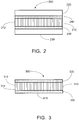
- FIG. 2 illustrates an embodiment of a thermal management assembly in accordance with aspects and embodiments of the invention.
- Thermal management assembly 200 comprises a bulk graphene core 210 disposed between substrates 220 and 230.
- the thermal management assembly 200 comprises thermal bond layers 240 and 250 disposed at the interface between the substrates and the bulk graphene core.
- Thermal bond layers 240 and 250 are metal-based coating interlayers comprising an additive or agent that can react with graphene to produce a carbide surface.
- the layers 240 and 250 are also referred to as "interlayers", "interface layers" or "filler".
- the bulk graphene core can be formed from a plurality of graphene layers being parallel to each other of at most 1 degree per mm in thickness.
- the term “bulk graphene” encompasses materials such as pyrolytic graphite ("PG"), thermal pyrolytic graphite (“TPG”), highly oriented pyrolytic graphite (“HOPG”), compression annealed pyrolytic graphite (“CAPG”), etc.
- PG pyrolytic graphite
- TPG thermal pyrolytic graphite
- HOPG highly oriented pyrolytic graphite
- CAG compression annealed pyrolytic graphite
- bulk graphene may also refer to graphite materials consisting of crystallites of considerable size, the crystallites being highly aligned or oriented with respect to each other and having well ordered carbon layers or a high degree of preferred crystallite orientation.
- Bulk graphene material mostly comprises carbon atoms arranged in hexagonal patterns within each plane.
- the bulk graphene material comprises at least 3000 graphene layers, the graphene layers being parallel to each other at an angle of at most 1 degree per mm in thickness.
- the graphene layers are at an angle between 0.001 degree and 1 degree per mm in thickness.
- the thickness of the bulk graphene is more than 1 um and size at least 1mm x 1mm. It exhibits high thermal conductivity, usually higher than 1000 W/m-K.
- the bulk graphene has an in-plane (a-b direction) thermal conductivity greater than 1000 W/m-K; greater than 1100 W/m-K; greater than 1200 W/m-K; even greater than 1500 W/m-K. In one embodiment, the bulk graphene has a thermal conductivity of from about 1000 W/m-K to about 1800 W/m-K; from about 1100 W/m-K to about 1700 W/m-K; even from about 1200 W/m-K to about 1500 W/m-K.
- the bulk graphene and thermal management assembly can also exhibit excellent through-plane thermal conductivity.
- the bulk graphene and/or thermal management assembly has a through-plane thermal conductivity of from about 200 W/m-K to about 1200 W/m-K; from about 400 W/m-K to about 1000 W/m-K; even from about 500 W/m-K to about 800 W/m-K.
- through-plane thermal conductivity of from about 200 W/m-K to about 1200 W/m-K; from about 400 W/m-K to about 1000 W/m-K; even from about 500 W/m-K to about 800 W/m-K.
- the bulk graphene can be provided in any suitable form.
- the bulk graphene is provided as a sheet.
- the bulk graphene core can have any size or thickness as desired for a particular purpose or intended use.
- the core can have a thickness of from about 0.001 mm to about 1mm, 1 mm to about 5 mm; from about 1.5 mm to about 4 mm; even from about 2 to about 3 mm.
- the core layer can have a thickness of from about 25% to about 95% of the total thickness of the thermal management assembly; from about 35% to about 90% of the total thickness of the thermal management assembly; from about 40% to about 80% of the total thickness of the thermal management assembly; even from about 50% to about 75% of the total thickness of the thermal management assembly.
- numerical values can be combined to form new and non-disclosed ranges.
- the core can be configured as desired for a particular purpose or intended application.
- the bulk graphene core is disposed in the assembly such that graphene planes are oriented substantially parallel to the substrates.
- the bulk graphene is disposed in the assembly such that the graphene planes are oriented perpendicular to the substrates.
- the graphene layers 212 are oriented perpendicular to the plane of the substrates.
- the bulk graphene core can be provided with vias.
- the loading density of the vias may range from less than 0.01% area of occupation to approximately 40% area of occupation. In another embodiment the via loading density may be from about 0.1% to about 20%.
- the spacing of the vias may range from about 0.5 to about 125 mm. In another embodiment, the spacing of the vias may range from about 1 to about 25 mm.
- a bulk graphene material with vias is described in U.S. Patent Publication No. 2010/0326645 .
- the substrate layers can be formed from any suitable metal or ceramic material as desired for a particular purpose or intended application.
- suitable metals for the substrate layer include, but are not limited to, copper, aluminum, tungsten, molybdenum, nickel, iron, tin, silver, gold, beryllium or alloys of two or more thereof.
- suitable ceramics include, but are not limited to, silicon nitride, silicon carbide, aluminum nitride, aluminum oxide, beryllium oxide, boron nitride, etc.
- the first and second substrates can be made from the same or different metal or ceramic materials.
- the thickness of the substrates can be selected as desired for a particular purpose or intended application. The thicknesses can be the same or different. In one embodiment, the substrates may each have a thickness of from about 2 microns to about 2 mm.
- the assembly of FIG. 2 shows substrates 220 and 230, it will be appreciated that the assembly can include one or more additional substrates overlying the substrates 220 and 230.
- the additional substrates can be formed from the same or different materials as substrates 220 or 230.
- the thermal management assembly comprises a metal-based coating disposed on opposing surfaces of the core.
- the metal-based material can serve as an outer layer or a layer for bonding the core layer to the substrates.
- the metal-based coating layer comprises an agent that can form a carbide with graphene at a sufficiently high temperature.
- the metal-based coating material has a lower melting temperature than either the bulk graphene or the substrates.
- the metal-based coating material has a thermal conductivity of about 20 W/m-K or greater.
- the metal-based coating material can comprise any suitable metal or alloy that melts and bonds to the surrounding metal or ceramic substrate at an elevated temperature lower than the substrate melting temperature and is independently chosen from silver, tin, lead, silver-copper, nickel or combinations of two or more thereof.
- the activating agent comprises a material that forms a carbide with graphene at a sufficiently high temperature.
- the activating agent is chosen from titanium, zirconium, chromium, hafnium, aluminum, tantalum, iron, silicon, or a combination of two or more thereof.
- suitable metal-based coatings that can be used to bond bulk graphene to various materials include but are not limited to Ag-Cu-Ti, Ti-Ni, Ni-Pd-Ti, Sn-Ti, Sn-Al, Sn-Ag-Ti, or a combination of two or more thereof.
- the metal-based coating material has a composition different than the composition of the substrate layers.
- FIG. 3 illustrates another embodiment of a thermal management assembly (not according to the present invention).
- thermal management assembly 300 comprises a bulk graphene core 310 having a first surface 312 and a second surface 314, a first outer layer 320 disposed on the first surface of the core, and a second outer layer 330 disposed on the second surface of the core.
- the core layer has the graphene layers 316 oriented perpendicular or parallel to the plane of the outer layers.
- the first and second outer layers are formed from a metal-based coating material.
- the metal-based coating material can be formed from an alloy comprising an agent that is reactive with the graphene to form a carbide.
- any of the materials that can be used as the interface material described above can be used to form the first and second outer layers.
- the metal-based coating layers can have a thickness of from about 0.01 mm to about 2 mm; from about 0.02 mm to about 1 mm; even from about 0.05mm to about 0.5 mm.
- numerical values can be combined to form new and non-disclosed ranges.
- the assembly of FIG. 3 can be used alone as a thermal management assembly or can be further modified to include one or more substrates in the assembly.
- a substrate could be disposed adjacent to the first outer layer 320.
- the assembly 300 could be modified by providing a first substrate adjacent to the first outer layer 320, and a second substrate adjacent to outer layer 330 to provide a thermal management assembly similar to that shown in FIG. 2 .
- the thermal management assembly exhibits good thermal conductivity.
- the thermal management assembly has a through-plane thermal conductivity of from about 200 W/m-K to about 1200 W/m-K; from about 400 W/m-K to about 1100 W/m-K; from about 500 W/m-K to about 1000 W/m-K; even from about 600 W/m-K to about 800 W/m-K.
- the thermal management assembly can have a relatively low thermal interface resistance.
- the thermal management assembly has a thermal interface resistance of less than 10 x10 -6 K-m 2 /W; less than 8 x 10 -6 K-m 2 /W; less than 5 x 10 -6 K-m 2 /W; less than 2 x 10 -6 K-m 2 /W; less than 1 x 10 -6 K-m 2 /W; less than 0.5 x 10 -6 K-m 2 /W; even less than 0.1 x 10 -6 K-m 2 /W.
- the thermal management assembly has a thermal interface resistance of from about 0.1 x 10 -6 K-m 2 /W to about 1 x 10 -6 K-m 2 /W; from about 0.2 x 10 -6 K-m 2 /W to about 0.8 x 10 -6 K-m 2 /W; even from about 0.3 x 10 -6 K-m 2 /W to about 0.6 x 10 -6 K-m 2 /W.
- a thermal interface resistance of from about 0.1 x 10 -6 K-m 2 /W to about 1 x 10 -6 K-m 2 /W; from about 0.2 x 10 -6 K-m 2 /W to about 0.8 x 10 -6 K-m 2 /W; even from about 0.3 x 10 -6 K-m 2 /W to about 0.6 x 10 -6 K-m 2 /W.
- a thermal management assembly can be formed by disposing a bulk graphene core material between two substrate layers and joining the substrate layers via the metal-based coating material.
- the metal-based coating material can be applied to opposing surfaces of the bulk graphene material, and the substrate material can be disposed on the surfaces of the bulk graphene comprising the metal-based coating material, the assembly can be subjected to joining under vacuum at a temperature above the melting temperature of the metal-based coating material and below the melting temperature of the core or the substrates.
- a poor interface can add a significant resistance to the heat flow and, thus, offset or even override the benefit of using the high thermal conductivity materials such as bulk graphene.
- the interface between bulk graphene and Cu showed high resistance due to lack of reaction and diffusion, which can result in an overall thermal conductivity lower than that of Cu.
- the diffusion bonding process exhibits issues of high complexity, high cost, application difficulty to ceramics and high temperature metals, and high interface resistance.
- Brazing and soldering on the other hand, rely on a molten filler metal to wet the mating surfaces of a joint, leading to the formation of metallurgical bonds.
- the metallic property of the brazing/soldering bond provides the continuity of high concentration of energy carriers (electrons), and, thus, renders a highly thermal conductive bond which can be referred to herein as a "thermal bond".
- Typical brazing or soldering fillers at molten format do not wet bulk graphene and do not spread freely to fill the gaps between bulk graphene and substrates. Such assemblies still exhibit relatively high thermal interface resistance due to the thermal barrier between bulk graphene and braze or solder.
- bulk graphene heat spreaders employing a metal-based interlayer between the core and the substrates with an agent that is reactive with graphene to form a carbide layer can provide an interface layer that bonds the core to the substrate and exhibits extremely low interface thermal resistance.
- the thermal management assembly can be sized and shape as desired for a particular purpose or intended use.
- the thermal management assembly can be used in an apparatus to aid in the thermal management of the apparatus.
- the thermal management assembly can be disposed adjacent a heat generating component in an apparatus and can dissipate the heat from heat generating component.
- the thermal management assembly can be used in devices in electronics such as computers, semiconductors, or any device where heat transfer between components is needed.
- the electronic component includes a semiconductor chip as a heat producing component.
- the heat producing component can be a chip carrier, an area array package, a chip scale package, or other semiconductor packaging structure.
- the semiconductor chip itself is the heat producing component.
- the hot device can be any hot device including, but not limited to, light emitting diodes, laser diodes, power amplifiers, MMIC's, IGBT's, ect.
- Composites are formed comprising two copper (Cu) substrates and a bulk graphene board disposed between the two metal layers.
- the bulk graphene material was thermal pyrolytic graphite.
- the bulk graphene board is oriented perpendicular to the Cu substrates so that the high thermal conductive path of the bulk graphene is aligned with the heat flow that comes through the layered structure.
- Ag-Cu with Ti additives is used to join the Cu and the bulk graphene at 850°C under vacuum.
- the prepared samples have a construction similar to the embodiment depicted in FIG. 2 .
- the thickness of the bulk graphene ranged from 37% to 87% of the total thickness of the composite.
- the thermal conductivity of the composites is evaluated by Netzsch NanoFlash LFA 447.
- FIG. 4 shows that the measured through-plane thermal conductivity with various bulk graphene loading matches the calculated value, indicating an excellent thermal bond between Cu and bulk graphene by employing the metal-based interlayer with the activating agent.
- FIG. 5 illustrates the thermal resistance of the composites formed according to aspects of the present invention.
- the present invention can provide composites with extremely low thermal resistance in the range of 10 -7 K-m 2 /W, and that the resistance is independent of the amount of bulk graphene loading.
- FIG. 6 compares the thermal resistance of these composites to those in accordance with aspects of the invention, and illustrates that the comparative composites have a thermal resistance at least an order of magnitude higher than the composites formed in accordance with aspects of the present invention.
Landscapes
- Engineering & Computer Science (AREA)
- Chemical & Material Sciences (AREA)
- Microelectronics & Electronic Packaging (AREA)
- Physics & Mathematics (AREA)
- Materials Engineering (AREA)
- Power Engineering (AREA)
- Computer Hardware Design (AREA)
- General Physics & Mathematics (AREA)
- Condensed Matter Physics & Semiconductors (AREA)
- Ceramic Engineering (AREA)
- Manufacturing & Machinery (AREA)
- General Engineering & Computer Science (AREA)
- Mechanical Engineering (AREA)
- Thermal Sciences (AREA)
- Cooling Or The Like Of Semiconductors Or Solid State Devices (AREA)
- Laminated Bodies (AREA)
- Carbon And Carbon Compounds (AREA)
- Cooling Or The Like Of Electrical Apparatus (AREA)
Description
- The present invention relates to a thermal management assembly that can be used to transfer heat away from a heat source; an assembly having the thermal management assembly in contact with the heat source; and methods of manufacturing such assemblies. In particular, the present invention relates to a thermal management assembly comprising bulk graphene materials.
- New electronic devices are constantly becoming more powerful and more compact. High power components, including RF/microwave electronics, diode laser, light emitting diode (LED), insulated gate bipolar transistors (IGBT), central processing units (CPU), etc., are utilized in a wide variety of industries such as telecommunications, automotive, aerospace, avionics, medical, and materials processing. With these smaller more powerful devices comes an increased requirement to dissipate the heat generated by the devices. The electronics can be damaged by temperature buildup if heat generated during operation is not sufficiently or effectively dissipated. New capabilities are constrained by the ability of designers to remove heat in a cost-effective manner. Generally, every 10°C increase in chip junction temperature cuts the life of the device in half.
- Conventional thermal management products are typically constructed of either copper (Cu) or aluminum (Al). But good thermal management and heat dissipation requires that the semiconductor die is bonded directly to the heat spreader, and conventional materials do not match the coefficient of thermal expansion of semiconductors. When directly bonded for optimum thermal management, thermal stress can impact the life of the assembly. Low coefficient of thermal expansion materials such as tungsten copper (WCu), molybdenum copper (MoCu), and aluminum silicon carbide (AlSiC) were developed to reduce the thermal stress between heat spreader and semiconductor die. To achieve necessary dielectric performance, aluminum nitride (AIN) and beryllium oxide (BeO) are also common choices as substrate materials for microelectronics.
- Other materials and designs have been disclosed for the management and removal of heat from electronic devices using bulk graphene materials.
U.S. Pat. No. 5,296,310 discloses a hybrid structural device of a high thermal conductivity material sandwiched between a pair of face sheets comprising a metal or matrix-reinforced metal. The core material can be a highly oriented pyrolytic graphite (HOPG), compression annealed pyrolytic graphite (CAPG), synthetic diamond, composites using these materials, or the like.U.S. Pat. No. 6,215,661 discloses a heat spreader comprising an L-shaped plate of thermal pyrolytic graphite encapsulated in aluminum.U.S. Pat. No. 5,958,572 discloses a heat spreading substrate comprising an insert of thermal pyrolytic graphite ("TPG"), a diamond like-carbon, or other similar material having a plurality of vias formed within to optimize heat flow transfer through the plurality of vias. - Thermal pyrolytic graphite (TPG), with its metal encapsulated composites (e.g., TC1050® available from Momentive Performance Materials), is an advanced thermal management material serving military and aerospace industries for over a decade. TPG is formed via a two-step process that provides well-aligned graphene planes to provide a material with superior thermal conductivity (e.g., greater than 1500 W/m-K). Compared to copper, which is commonly used in passive cooling and most thermal conductive among all the materials mentioned above, TPG can provide four times the cooling power at 1/4th the weight of copper.
- Bulk graphene material, including the above described materials, is a relatively soft material, due to its weak Van de Waals force between the graphene layers. Traditionally, heat spreaders comprising bulk graphene are formed by encapsulating bulk graphene into a metal casing, such as aluminum, copper, etc. via a diffusion bonding process. Such a process is described in
U.S. Patent No. 6,661,317 . The encapsulated bulk graphene composite parts behave like solid metal and can be further machined, plated, or bonded to other components to meet various customers' requirement. A typical manufacturing process is illustrated inFIGs. 1A-1C . A bulk graphene-metal composite 100 can be formed by (A) disposing abulk graphene core 112 betweenmetal face sheets - Encapsulated bulk graphene composites, such as cold plates, heat spreaders, thermal straps, etc., can quickly conduct the heat away from the heat source and, greatly increase the electronic device's efficiency and life. Over the years, bulk graphene-metal composites have been successfully implemented into the cooling systems in satellites, avionics, and phased array radars, which can take full advantage of its high thermal performance, high durability, and light weight.
- However, the interdiffusion between aluminum/copper and bulk graphene requires high temperature and high pressure, which makes the diffusion bonding process quite complex and extremely expensive. It becomes more challenging when high melting temperature alloys, such as tungsten and molybdenum, are used for encapsulation. The stiffness, brittleness of ceramics substrates and extremely high temperature stability of ceramics makes the bonding of ceramics with bulk graphene directly under heat and pressure an especially challenging process, which essentially eliminates it as an option to form such structures. These limitations of diffusion bonding hinder the development of bulk graphene composites.
-
US 5 195 021 A describes a thermal core comprising a graphite layer held between two molybdenum layers for dissipating heat from a plurality of chip carriers. -
US 2012/0234524 A1 discloses a high thermal conductivity/low coefficient of thermal expansion thermally conductive composite material for heat sinks. - Herein, it is described a thermal management assembly comprising a metal-based thermal bond disposed between a bulk graphene core material and a surrounding metal or ceramic substrate. The metal-based interlayer comprises a material that is reactive with the graphene to form a carbide. The metal-based interlayer provides an interface with the bulk graphene core that allows for excellent thermal conductivity and low thermal resistance.
- In one aspect, the present invention provides a thermal management assembly that exhibits low thermal interface resistance. The present invention can even provide a thermal interface that is orders of magnitude lower than conventional thermal interface assemblies.
- The present invention provides a thermal management assembly comprising a first substrate; a second substrate; a bulk graphene material disposed between the first and second substrates; and a thermal bond disposed between (a) a first surface of the bulk graphene layer and the first substrate, and (b) a second surface of the bulk graphene layer and the second substrate, the thermal bonds comprising (i) a metal-based material comprising (ii) an agent that is reactive with the graphene to form a carbide, wherein the agent is chosen from titanium, zirconium, chromium, hafnium, aluminum, tantalum, iron, silicon, or a combination of two or more thereof, and the metal-based material of the thermal bond layers is independently chosen from silver, tin, lead, silver-copper, nickel or combinations of two or more thereof.
- Herein, it is described a thermal management assembly comprising a bulk graphene core material having a first surface and a second surface opposite the first surface; a first outer layer disposed on the first surface of the core material; and a second outer layer disposed on the second surface of the core material; wherein the first outer layer and the second outer layer are independently formed from a metal-based material comprising an agent that is reactive with graphene to form a carbide.
- The thermal management assembly can have a thermal interface resistance of less than 10 x10-6 K-m2/W; less than 8 x 10⁻⁶ K-m2/W; less than 5 x 10⁻⁶ K-m2/W; less than 2 x 10⁻⁶ K-m2/W; less than 1 x 10⁻⁶ K-m2/W; less than 0.5 x 10⁻⁶ K-m2/W; even less than 0.1 x 10⁻⁶ K-m2/W.
-
FIGS. 1A-1C illustrates a heat spreader comprising bulk graphene encapsulated by metal via a diffusion bonding process; -
FIG. 2 is a cross-sectional view of a thermal management assembly in accordance with an embodiment of the present invention; -
FIG.3 is cross-sectional view of another embodiment of a thermal management assembly (not according to the present invention); -
FIG.4 is a graph illustrating the through plane thermal conductivity of a thermal management assembly in accordance with an embodiment of the invention; -
FIG.5 is a graph illustrating the thermal interface resistance of a thermal management assembly in accordance with the an embodiment of the present invention at different bulk graphene loadings; and -
FIG.6 is a graph illustrating the thermal resistance of thermal management assemblies formed by different manufacturing methods. - The present invention provides a thermal management assembly comprising a bulk graphene core material and a metal-based coating layer disposed on surfaces of the graphene layer. The metal-based coating comprises a material that is reactive with graphene to form a carbide. The metal-based coating provides an interface with the bulk graphene core that allows for excellent thermal conductivity and low thermal resistance. The thermal management assembly can comprise a structure comprising a bulk graphene core having the metal-based coating layer disposed on the surfaces of the bulk graphene material. In one embodiment, a thermal management assembly comprises the metal-based coating disposed between a bulk graphene core material and outer metal or ceramic substrates.
- As used herein, the term "thermal management assembly" refers to a thermal management device or a heat transfer device comprising a high thermal conductivity material for dissipating or removing heat from a heat source. A thermal management assembly can include, but is not limited to, heat spreaders, heat sinks, cold plates, etc.
- The metal-based coating layer comprising a material that is reactive with graphene to form a carbide may also be referred to herein as a "thermal bond layer." Depending on the structure, the metal-based coating layer can also be referred to as an interlayer disposed between a surface of the graphene core material and a substrate.
-
FIG. 2 illustrates an embodiment of a thermal management assembly in accordance with aspects and embodiments of the invention.Thermal management assembly 200 comprises abulk graphene core 210 disposed betweensubstrates thermal management assembly 200 comprises thermal bond layers 240 and 250 disposed at the interface between the substrates and the bulk graphene core. Thermal bond layers 240 and 250 are metal-based coating interlayers comprising an additive or agent that can react with graphene to produce a carbide surface. In the embodiment ofFIG. 2 , thelayers - The bulk graphene core can be formed from a plurality of graphene layers being parallel to each other of at most 1 degree per mm in thickness. As used herein, the term "bulk graphene" encompasses materials such as pyrolytic graphite ("PG"), thermal pyrolytic graphite ("TPG"), highly oriented pyrolytic graphite ("HOPG"), compression annealed pyrolytic graphite ("CAPG"), etc. In one embodiment, bulk graphene may also refer to graphite materials consisting of crystallites of considerable size, the crystallites being highly aligned or oriented with respect to each other and having well ordered carbon layers or a high degree of preferred crystallite orientation. Bulk graphene material mostly comprises carbon atoms arranged in hexagonal patterns within each plane. In one embodiment, the bulk graphene material comprises at least 3000 graphene layers, the graphene layers being parallel to each other at an angle of at most 1 degree per mm in thickness. In one embodiment, the graphene layers are at an angle between 0.001 degree and 1 degree per mm in thickness. The thickness of the bulk graphene is more than 1 um and size at least 1mm x 1mm. It exhibits high thermal conductivity, usually higher than 1000 W/m-K. In one embodiment, the bulk graphene has an in-plane (a-b direction) thermal conductivity greater than 1000 W/m-K; greater than 1100 W/m-K; greater than 1200 W/m-K; even greater than 1500 W/m-K. In one embodiment, the bulk graphene has a thermal conductivity of from about 1000 W/m-K to about 1800 W/m-K; from about 1100 W/m-K to about 1700 W/m-K; even from about 1200 W/m-K to about 1500 W/m-K. The bulk graphene and thermal management assembly can also exhibit excellent through-plane thermal conductivity. In one embodiment, the bulk graphene and/or thermal management assembly has a through-plane thermal conductivity of from about 200 W/m-K to about 1200 W/m-K; from about 400 W/m-K to about 1000 W/m-K; even from about 500 W/m-K to about 800 W/m-K. Here as elsewhere in the specification and claims, numerical values can be combined to form new and non-disclosed ranges.
- The bulk graphene can be provided in any suitable form. In one embodiment, the bulk graphene is provided as a sheet. The bulk graphene core can have any size or thickness as desired for a particular purpose or intended use. In one embodiment, the core can have a thickness of from about 0.001 mm to about 1mm, 1 mm to about 5 mm; from about 1.5 mm to about 4 mm; even from about 2 to about 3 mm. In one embodiment, the core layer can have a thickness of from about 25% to about 95% of the total thickness of the thermal management assembly; from about 35% to about 90% of the total thickness of the thermal management assembly; from about 40% to about 80% of the total thickness of the thermal management assembly; even from about 50% to about 75% of the total thickness of the thermal management assembly. Here as elsewhere in the specification and claims, numerical values can be combined to form new and non-disclosed ranges.
- The core can be configured as desired for a particular purpose or intended application. In one embodiment, the bulk graphene core is disposed in the assembly such that graphene planes are oriented substantially parallel to the substrates. In another embodiment, the bulk graphene is disposed in the assembly such that the graphene planes are oriented perpendicular to the substrates. In
FIG. 2 , the graphene layers 212 are oriented perpendicular to the plane of the substrates. - In one embodiment, the bulk graphene core can be provided with vias. The loading density of the vias may range from less than 0.01% area of occupation to approximately 40% area of occupation. In another embodiment the via loading density may be from about 0.1% to about 20%. In one embodiment, the spacing of the vias may range from about 0.5 to about 125 mm. In another embodiment, the spacing of the vias may range from about 1 to about 25 mm. A bulk graphene material with vias is described in
U.S. Patent Publication No. 2010/0326645 . - The substrate layers can be formed from any suitable metal or ceramic material as desired for a particular purpose or intended application. Examples of suitable metals for the substrate layer include, but are not limited to, copper, aluminum, tungsten, molybdenum, nickel, iron, tin, silver, gold, beryllium or alloys of two or more thereof. Examples of suitable ceramics include, but are not limited to, silicon nitride, silicon carbide, aluminum nitride, aluminum oxide, beryllium oxide, boron nitride, etc. The first and second substrates can be made from the same or different metal or ceramic materials. The thickness of the substrates can be selected as desired for a particular purpose or intended application. The thicknesses can be the same or different. In one embodiment, the substrates may each have a thickness of from about 2 microns to about 2 mm.
- While the assembly of
FIG. 2 showssubstrates substrates substrates - The thermal management assembly comprises a metal-based coating disposed on opposing surfaces of the core. The metal-based material can serve as an outer layer or a layer for bonding the core layer to the substrates. The metal-based coating layer comprises an agent that can form a carbide with graphene at a sufficiently high temperature. Generally, the metal-based coating material has a lower melting temperature than either the bulk graphene or the substrates. In one embodiment, the metal-based coating material has a thermal conductivity of about 20 W/m-K or greater. The metal-based coating material can comprise any suitable metal or alloy that melts and bonds to the surrounding metal or ceramic substrate at an elevated temperature lower than the substrate melting temperature and is independently chosen from silver, tin, lead, silver-copper, nickel or combinations of two or more thereof. The activating agent comprises a material that forms a carbide with graphene at a sufficiently high temperature. The activating agent is chosen from titanium, zirconium, chromium, hafnium, aluminum, tantalum, iron, silicon, or a combination of two or more thereof. Examples of suitable metal-based coatings that can be used to bond bulk graphene to various materials include but are not limited to Ag-Cu-Ti, Ti-Ni, Ni-Pd-Ti, Sn-Ti, Sn-Al, Sn-Ag-Ti, or a combination of two or more thereof. In one embodiment, the metal-based coating material has a composition different than the composition of the substrate layers.
-
FIG. 3 illustrates another embodiment of a thermal management assembly (not according to the present invention). InFIG. 3 ,thermal management assembly 300 comprises abulk graphene core 310 having afirst surface 312 and asecond surface 314, a firstouter layer 320 disposed on the first surface of the core, and a secondouter layer 330 disposed on the second surface of the core. The core layer has the graphene layers 316 oriented perpendicular or parallel to the plane of the outer layers. The first and second outer layers are formed from a metal-based coating material. In one embodiment, the metal-based coating material can be formed from an alloy comprising an agent that is reactive with the graphene to form a carbide. In this embodiment, any of the materials that can be used as the interface material described above can be used to form the first and second outer layers. - The metal-based coating layers can have a thickness of from about 0.01 mm to about 2 mm; from about 0.02 mm to about 1 mm; even from about 0.05mm to about 0.5 mm. Here as elsewhere in the specification and claims, numerical values can be combined to form new and non-disclosed ranges.
- The assembly of
FIG. 3 can be used alone as a thermal management assembly or can be further modified to include one or more substrates in the assembly. For example, in one embodiment a substrate could be disposed adjacent to the firstouter layer 320. In another embodiment, theassembly 300 could be modified by providing a first substrate adjacent to the firstouter layer 320, and a second substrate adjacent toouter layer 330 to provide a thermal management assembly similar to that shown inFIG. 2 . - The thermal management assembly exhibits good thermal conductivity. In one embodiment, the thermal management assembly has a through-plane thermal conductivity of from about 200 W/m-K to about 1200 W/m-K; from about 400 W/m-K to about 1100 W/m-K; from about 500 W/m-K to about 1000 W/m-K; even from about 600 W/m-K to about 800 W/m-K. The thermal management assembly can have a relatively low thermal interface resistance. In one embodiment, the thermal management assembly has a thermal interface resistance of less than 10 x10-6 K-m2/W; less than 8 x 10⁻⁶ K-m2/W; less than 5 x 10⁻⁶ K-m2/W; less than 2 x 10⁻⁶ K-m2/W; less than 1 x 10⁻⁶ K-m2/W; less than 0.5 x 10⁻⁶ K-m2/W; even less than 0.1 x 10⁻⁶ K-m2/W. In one embodiment, the thermal management assembly has a thermal interface resistance of from about 0.1 x 10⁻⁶ K-m2/W to about 1 x 10⁻⁶ K-m2/W; from about 0.2 x 10⁻⁶ K-m2/W to about 0.8 x 10⁻⁶ K-m2/W; even from about 0.3 x 10⁻⁶ K-m2/W to about 0.6 x 10⁻⁶ K-m2/W. Here as elsewhere in the specification and claims, numerical values can be combined to form new and non-disclosed ranges.
- A thermal management assembly can be formed by disposing a bulk graphene core material between two substrate layers and joining the substrate layers via the metal-based coating material. The metal-based coating material can be applied to opposing surfaces of the bulk graphene material, and the substrate material can be disposed on the surfaces of the bulk graphene comprising the metal-based coating material, the assembly can be subjected to joining under vacuum at a temperature above the melting temperature of the metal-based coating material and below the melting temperature of the core or the substrates.
- As described above, the present invention provides a thermal management assembly with good thermal conductivity and, in one embodiment, a low thermal interface resistance. Due to the differences in electronic and vibrational properties in different materials, when an energy carrier attempts to traverse the interface, it scatters at the interface. For thermal management assemblies comprising layers formed from different thermal management materials a poor thermal interface can contribute to interface scattering. Theoretically the thermal resistance through multiple layers can be presented as:

- A poor interface can add a significant resistance to the heat flow and, thus, offset or even override the benefit of using the high thermal conductivity materials such as bulk graphene. For example, for assemblies formed by other processes such as conventional diffusion or brazing, the interface between bulk graphene and Cu showed high resistance due to lack of reaction and diffusion, which can result in an overall thermal conductivity lower than that of Cu.
- Common methods of joining dissimilar materials include mechanical fastening, adhesive bonding, welding, solid state joining, brazing and soldering. Mechanical fastening inevitably leaves a thin gap between the two materials, which is a significant thermal barrier to the heat flow and, therefore, is considered the worst type of joining for heat conduction. Fluid adhesive before curing can fill up the spaces at the interface, but its polymer heritage determines its low thermal conductivity (typically less than 10 W/m-K), which is far less than most of the metals. Welding of high temperature materials is difficult, such as joining W or Mo, and sometimes is impossible when ceramics or graphite is involved. Solid state joining includes diffusion bonding, which was developed for bonding bulk graphene with various metals in the past. As discussed in the previous paragraphs, the diffusion bonding process exhibits issues of high complexity, high cost, application difficulty to ceramics and high temperature metals, and high interface resistance. Brazing and soldering, on the other hand, rely on a molten filler metal to wet the mating surfaces of a joint, leading to the formation of metallurgical bonds. The metallic property of the brazing/soldering bond provides the continuity of high concentration of energy carriers (electrons), and, thus, renders a highly thermal conductive bond which can be referred to herein as a "thermal bond". Typical brazing or soldering fillers at molten format, however, do not wet bulk graphene and do not spread freely to fill the gaps between bulk graphene and substrates. Such assemblies still exhibit relatively high thermal interface resistance due to the thermal barrier between bulk graphene and braze or solder.
- On the other hand, the inventors have found that bulk graphene heat spreaders employing a metal-based interlayer between the core and the substrates with an agent that is reactive with graphene to form a carbide layer can provide an interface layer that bonds the core to the substrate and exhibits extremely low interface thermal resistance.
- The thermal management assembly can be sized and shape as desired for a particular purpose or intended use. The thermal management assembly can be used in an apparatus to aid in the thermal management of the apparatus. The thermal management assembly can be disposed adjacent a heat generating component in an apparatus and can dissipate the heat from heat generating component. The thermal management assembly can be used in devices in electronics such as computers, semiconductors, or any device where heat transfer between components is needed. In one embodiment, the electronic component includes a semiconductor chip as a heat producing component. In such a case, the heat producing component can be a chip carrier, an area array package, a chip scale package, or other semiconductor packaging structure. In other embodiments the semiconductor chip itself is the heat producing component. The hot device can be any hot device including, but not limited to, light emitting diodes, laser diodes, power amplifiers, MMIC's, IGBT's, ect.
- The invention will now be described and may be further understood with respect to the following examples. The examples are intended to be illustrative only and are to be understood as not limiting the invention disclosed herein in any way as to materials, or process parameters, equipment or conditions.
- Composites are formed comprising two copper (Cu) substrates and a bulk graphene board disposed between the two metal layers. In the Examples, the bulk graphene material was thermal pyrolytic graphite. The bulk graphene board is oriented perpendicular to the Cu substrates so that the high thermal conductive path of the bulk graphene is aligned with the heat flow that comes through the layered structure. Ag-Cu with Ti additives is used to join the Cu and the bulk graphene at 850°C under vacuum. The prepared samples have a construction similar to the embodiment depicted in
FIG. 2 . The thickness of the bulk graphene ranged from 37% to 87% of the total thickness of the composite. - The thermal conductivity of the composites is evaluated by Netzsch NanoFlash LFA 447. For a layered structure free of interface thermal resistance, the overall thermal conductivity of the bulk graphene composite can be calculated as:

FIG. 4 shows that the measured through-plane thermal conductivity with various bulk graphene loading matches the calculated value, indicating an excellent thermal bond between Cu and bulk graphene by employing the metal-based interlayer with the activating agent. - The thermal resistance can be estimated by comparing the difference between the theoretical and experimental thermal conductivity, according to the following formula:

-
FIG. 5 illustrates the thermal resistance of the composites formed according to aspects of the present invention. As shown inFIG. 5 , the present invention can provide composites with extremely low thermal resistance in the range of 10-7 K-m2/W, and that the resistance is independent of the amount of bulk graphene loading. - Cu/bulk graphene/Cu samples are also prepared via adhesive bonding, diffusion bonding, and conventional brazing.
FIG. 6 compares the thermal resistance of these composites to those in accordance with aspects of the invention, and illustrates that the comparative composites have a thermal resistance at least an order of magnitude higher than the composites formed in accordance with aspects of the present invention.
Claims (14)
- A thermal management assembly (200) comprising:a first substrate (220, 230);a second substrate (220, 230);a bulk graphene material (210) disposed between the first and second substrates (220, 230); anda thermal bond layer (240, 250) disposed between (a) a first surface of the bulk graphene layer (210) and the first substrate (220, 230), and (b) a second surface of the bulk graphene layer (210) and the second substrate (220, 230), the thermal bond layers (240, 250) comprising (i) a metal-based material comprising (ii) an agent that is reactive with the graphene to form a carbide,characterized in that the agent is chosen from titanium, zirconium, chromium, hafnium, aluminum, tantalum, iron, silicon, or a combination of two or more thereof, and
the metal-based material of the thermal bond layers (240, 250) is independently chosen from silver, tin, lead, silver-copper, nickel or combinations of two or more thereof. - The thermal management assembly (200) of claim 1, wherein the bulk graphene material (210) comprises at least 3000 graphene layers (212), the graphene layers (212) being parallel to each other at an angle of at most 1 degree per mm in thickness.
- The thermal management assembly (200) of claim 2, wherein the bulk graphene material (210) exhibits an in-plane thermal conductivity at least of 1000 W/m·K.
- The thermal management assembly (200) of claims 1-3, wherein the thermal bond layers (240, 250) independently have a thermal conductivity of about 20 W/m·K or greater, and a melting temperature less than the melting temperature of the substrates (220, 230) and the melting temperature of the bulk graphene.
- The thermal management assembly (200) any of claims 1-4, wherein the first substrate (220, 230) and the second substrate (220, 230) independently comprise a metal or a ceramic material.
- The thermal management assembly (200) any of claims 1-5, wherein the first substrate (220, 230) and the second substrate (220, 230) independently comprise copper, aluminum, tungsten, molybdenum, nickel, iron, tin, silver, gold, beryllium, or alloys of two or more thereof.
- The thermal management assembly (200) any of claims 1-5, wherein the first substrate (220, 230) and the second substrate (220, 230) independently comprise silicon nitride, silicon carbide, aluminum nitride, aluminum oxide, beryllium oxide, boron nitride, or a combination of two or more thereof.
- The thermal management assembly (200) any of claims 1-5, wherein the first substrate (220, 230) comprises copper, aluminum, tungsten, molybdenum, nickel, iron, tin, silver, gold, beryllium, or alloys of two or more thereof, and the second substrate (220, 230) comprises silicon nitride, silicon carbide, aluminum nitride, aluminum oxide, beryllium oxide, boron nitride, or a combination of two or more thereof.
- The thermal management assembly (200) any of claims 1-8, wherein the bulk graphene material (210) has a thickness from about 25% to about 95% of the total thickness of the thermal management assembly (200), preferably from about 35% to about 90% of the total thickness of the thermal management assembly (200).
- The thermal management assembly (200) of any of claims 1-9, wherein the bulk graphene material (210) is chosen from pyrolytic graphite, thermal pyrolytic graphite, highly oriented pyrolytic graphite, compression annealed pyrolytic graphite, or a combination of two or more thereof.
- The thermal management assembly (200) any of claims 1-10, wherein the bulk graphene material (210) comprises at least 3000 of graphene layers (212), and the bulk graphene material (210) is disposed in the assembly (200) such that the graphene layers (212) are oriented perpendicular to the first and second substrates (220, 230).
- The thermal management assembly (200) of claim 11, having a through- plane thermal conductivity of from about 200 W/m·K to about 1200 W/m·K.
- The thermal management assembly (200) of any of claims 1-12, wherein the thermal bond has a thermal resistance of less than 10 x 10-6 K·m2/W, preferably less than 5 x 10⁻⁶ K·m2/W, more preferably less than 1 x 10⁻⁶ K·m2/W, even more preferably less than 0.5 x 10⁻⁶ K·m2/W, still even more preferably less than 0.1 x 10⁻⁶ K·m2/W.
- An apparatus comprising a heat generating component and the thermal management assembly (200) of any of claims 1-13 disposed adjacent the heat generating component such that heat from the heat generating component can be transferred through the thermal management assembly (200).
Applications Claiming Priority (2)
| Application Number | Priority Date | Filing Date | Title |
|---|---|---|---|
| US201261705362P | 2012-09-25 | 2012-09-25 | |
| PCT/US2013/061335 WO2014052282A1 (en) | 2012-09-25 | 2013-09-24 | Thermal management assembly comprising bulk graphene material |
Publications (3)
| Publication Number | Publication Date |
|---|---|
| EP2901826A1 EP2901826A1 (en) | 2015-08-05 |
| EP2901826A4 EP2901826A4 (en) | 2016-06-15 |
| EP2901826B1 true EP2901826B1 (en) | 2020-12-16 |
Family
ID=50388897
Family Applications (1)
| Application Number | Title | Priority Date | Filing Date |
|---|---|---|---|
| EP13840941.2A Active EP2901826B1 (en) | 2012-09-25 | 2013-09-24 | Thermal management assembly comprising bulk graphene material |
Country Status (5)
| Country | Link |
|---|---|
| US (1) | US11105567B2 (en) |
| EP (1) | EP2901826B1 (en) |
| JP (1) | JP6529433B2 (en) |
| CN (1) | CN104813751B (en) |
| WO (1) | WO2014052282A1 (en) |
Families Citing this family (42)
| Publication number | Priority date | Publication date | Assignee | Title |
|---|---|---|---|---|
| US9634214B2 (en) * | 2012-11-05 | 2017-04-25 | Ledengin, Inc. | Graphite-containing substrates for LED packages |
| CN104754913B (en) * | 2013-12-27 | 2018-06-05 | 华为技术有限公司 | Heat-conductive composite material piece and preparation method thereof |
| KR102374256B1 (en) * | 2015-02-23 | 2022-03-15 | 삼성전기주식회사 | Circuit board and manufacturing method thereof |
| CN107835916A (en) * | 2015-05-15 | 2018-03-23 | 莫门蒂夫性能材料股份有限公司 | The light-emitting diode component of heat management is carried out using pyrolytic graphite |
| CN107686699B (en) * | 2016-08-05 | 2021-07-16 | 中兴通讯股份有限公司 | Heat-conducting interface material and preparation method thereof |
| US10139168B2 (en) * | 2016-09-26 | 2018-11-27 | International Business Machines Corporation | Cold plate with radial expanding channels for two-phase cooling |
| WO2018117232A1 (en) * | 2016-12-22 | 2018-06-28 | 京セラ株式会社 | Substrate for mounting electronic element, electronic device and electronic module |
| EP3352213B1 (en) | 2017-01-23 | 2021-10-06 | ABB Power Grids Switzerland AG | Semiconductor power module comprising graphene |
| JP6754973B2 (en) * | 2017-02-02 | 2020-09-16 | パナソニックIpマネジメント株式会社 | Graphite radiator plate |
| KR102469901B1 (en) * | 2017-04-07 | 2022-11-22 | 에스케이넥실리스 주식회사 | Graphite Heat Dissipation Film With Copper Foil Lamination |
| KR20190003186A (en) * | 2017-06-30 | 2019-01-09 | 주식회사 솔루에타 | Heat radiation thin film and method of fabricating of the same |
| US10455736B2 (en) | 2017-07-21 | 2019-10-22 | Raytheon Company | Reduced cost and schedule manufacturing of graphene paper based thermal straps/harnesses |
| CN111356544B (en) * | 2017-11-20 | 2022-01-14 | 三菱综合材料株式会社 | Composite heat transfer member and method for manufacturing composite heat transfer member |
| EP3488999B1 (en) * | 2017-11-24 | 2023-03-08 | Airbus Operations, S.L. | Joining method for thermoplastic elements |
| US11476399B2 (en) | 2017-11-29 | 2022-10-18 | Panasonic Intellectual Property Management Co., Ltd. | Jointing material, fabrication method for semiconductor device using the jointing material, and semiconductor device |
| JP7108907B2 (en) * | 2017-11-29 | 2022-07-29 | パナソニックIpマネジメント株式会社 | Bonding material, method for manufacturing semiconductor device using bonding material, and semiconductor device |
| CN111656515B (en) * | 2018-01-30 | 2024-04-26 | 京瓷株式会社 | Electronic component mounting substrate, electronic device, and electronic module |
| US11152279B2 (en) * | 2018-03-26 | 2021-10-19 | Raytheon Company | Monolithic microwave integrated circuit (MMIC) cooling structure |
| US20190301814A1 (en) * | 2018-04-03 | 2019-10-03 | Nanotek Instruments, Inc. | Metallized graphene foam having high through-plane conductivity |
| WO2020056165A1 (en) * | 2018-09-14 | 2020-03-19 | Raytheon Company | Module base with integrated thermal spreader and heat sink for thermal and structural management of high-performance integrated circuits or other devices |
| KR102600004B1 (en) * | 2018-12-26 | 2023-11-08 | 삼성전자주식회사 | Semiconductor package |
| CN110004442A (en) * | 2018-12-27 | 2019-07-12 | 岑对凤 | A kind of superconduction composite plate and its manufacturing method |
| CN112941443B (en) * | 2019-01-30 | 2022-11-04 | 浙江华达新型材料股份有限公司 | Coating type preparation process for plating coating on surface of steel plate |
| CN110602871B (en) * | 2019-09-16 | 2021-10-01 | 沪士电子股份有限公司 | Graphene heat-conducting PCB and preparation method thereof |
| JP7533124B2 (en) | 2019-11-05 | 2024-08-14 | 三菱マテリアル株式会社 | Graphene-containing carbonaceous member/ceramic joint, and copper/graphene-containing carbonaceous member/ceramic joint |
| WO2021090759A1 (en) * | 2019-11-05 | 2021-05-14 | 三菱マテリアル株式会社 | Graphene-containing carbonaceous member/ceramic assembly and copper/graphene-containing carbonaceous member/ceramic assembly |
| WO2021106904A1 (en) * | 2019-11-25 | 2021-06-03 | 三菱マテリアル株式会社 | Graphene bonded body |
| JP7563124B2 (en) | 2019-11-25 | 2024-10-08 | 三菱マテリアル株式会社 | Graphene Joints |
| WO2021149802A1 (en) * | 2020-01-24 | 2021-07-29 | 三菱マテリアル株式会社 | Copper/graphene joined body and method for manufacturing same, and copper/graphene joined structure |
| JP6947318B2 (en) * | 2020-01-24 | 2021-10-13 | 三菱マテリアル株式会社 | Copper / graphene junction and its manufacturing method, and copper / graphene junction structure |
| US11032947B1 (en) * | 2020-02-17 | 2021-06-08 | Raytheon Company | Tailored coldplate geometries for forming multiple coefficient of thermal expansion (CTE) zones |
| CN112543580B (en) * | 2020-11-17 | 2022-04-15 | 河北北方学院 | Production process of high-thermal-conductivity graphene-metal copper composite layer radiator |
| CN112693636A (en) * | 2020-12-28 | 2021-04-23 | 上海卫星工程研究所 | Light-weight thermal control device for satellite and manufacturing method thereof |
| TWI833063B (en) * | 2021-01-27 | 2024-02-21 | 大陸商河南烯力新材料科技有限公司 | Thermal conductive structure and electronic device |
| US12004308B2 (en) * | 2021-05-18 | 2024-06-04 | Mellanox Technologies, Ltd. | Process for laminating graphene-coated printed circuit boards |
| US11963309B2 (en) | 2021-05-18 | 2024-04-16 | Mellanox Technologies, Ltd. | Process for laminating conductive-lubricant coated metals for printed circuit boards |
| JP2023006510A (en) | 2021-06-30 | 2023-01-18 | 日亜化学工業株式会社 | Light-emitting module, vehicle lamp, and heat dissipation member |
| US11849536B1 (en) | 2022-10-12 | 2023-12-19 | Lunar Energy, Inc. | Gantry for thermal management |
| US11997812B2 (en) | 2022-10-12 | 2024-05-28 | Lunar Energy, Inc. | Cover for sealing a power module |
| US11889662B1 (en) * | 2022-10-12 | 2024-01-30 | Lunar Energy, Inc. | Thermal interface sandwich |
| CN118354563A (en) * | 2023-01-13 | 2024-07-16 | 华为技术有限公司 | Graphene plate, preparation method, heat dissipation module and electronic equipment |
| CN115799974B (en) * | 2023-02-07 | 2023-05-26 | 度亘激光技术(苏州)有限公司 | Heat conduction structure, preparation method thereof and indirect heat conduction structure |
Family Cites Families (26)
| Publication number | Priority date | Publication date | Assignee | Title |
|---|---|---|---|---|
| US4104417A (en) * | 1973-03-12 | 1978-08-01 | Union Carbide Corporation | Method of chemically bonding aluminum to carbon substrates via monocarbides |
| AT389832B (en) * | 1988-08-01 | 1990-02-12 | Plansee Metallwerk | SOLDER CONNECTION |
| US4963414A (en) * | 1989-06-12 | 1990-10-16 | General Electric Company | Low thermal expansion, heat sinking substrate for electronic surface mount applications |
| JPH03136397A (en) * | 1989-08-21 | 1991-06-11 | Texas Instr Inc <Ti> | Forced core for surface carrying technique and its manufacturing method |
| US5195021A (en) | 1989-08-21 | 1993-03-16 | Texas Instruments Incorporated | Constraining core for surface mount technology |
| US5296310A (en) | 1992-02-14 | 1994-03-22 | Materials Science Corporation | High conductivity hydrid material for thermal management |
| US5494753A (en) * | 1994-06-20 | 1996-02-27 | General Electric Company | Articles having thermal conductors of graphite |
| US6131651A (en) * | 1998-09-16 | 2000-10-17 | Advanced Ceramics Corporation | Flexible heat transfer device and method |
| US5958572A (en) | 1997-09-30 | 1999-09-28 | Motorola, Inc. | Hybrid substrate for cooling an electronic component |
| US6075701A (en) * | 1999-05-14 | 2000-06-13 | Hughes Electronics Corporation | Electronic structure having an embedded pyrolytic graphite heat sink material |
| US6215661B1 (en) | 1999-08-11 | 2001-04-10 | Motorola, Inc. | Heat spreader |
| US6661317B2 (en) | 2002-03-13 | 2003-12-09 | The Boeing Co. | Microwave monolithic integrated circuit assembly with multi-orientation pyrolytic graphite heat-dissipating assembly |
| US7220485B2 (en) * | 2003-09-19 | 2007-05-22 | Momentive Performance Materials Inc. | Bulk high thermal conductivity feedstock and method of making thereof |
| CN100496186C (en) * | 2003-09-19 | 2009-06-03 | 通用电气公司 | Bulk high thermal conductivity material and method of making thereof |
| JP2005159318A (en) * | 2003-11-04 | 2005-06-16 | Otsuka Denki Kk | Heat conductor |
| EP1680274B1 (en) | 2003-11-04 | 2018-09-26 | NeoGraf Solutions, LLC | Sandwiched thermal solution |
| US20070053168A1 (en) * | 2004-01-21 | 2007-03-08 | General Electric Company | Advanced heat sinks and thermal spreaders |
| US20100326645A1 (en) * | 2004-01-21 | 2010-12-30 | Wei Fan | Thermal pyrolytic graphite laminates with vias |
| AT7807U1 (en) * | 2004-09-06 | 2005-09-26 | Plansee Ag | COMPOSITE MATERIAL |
| JP2006196593A (en) | 2005-01-12 | 2006-07-27 | Sumitomo Electric Ind Ltd | Semiconductor device and heat sink |
| JP5098642B2 (en) * | 2005-06-16 | 2012-12-12 | パナソニック株式会社 | Method for producing heat-dissipating graphite sheet |
| US20070289730A1 (en) | 2006-06-06 | 2007-12-20 | Chang-Hsin Wu | Combination heat-transfer plate member |
| JP2011023670A (en) | 2009-07-17 | 2011-02-03 | Thermo Graphitics Co Ltd | Anisotropic thermally-conductive element, and method of manufacturing the same |
| US20110070459A1 (en) * | 2009-09-18 | 2011-03-24 | Irwin In Kim | Thermal Management System |
| US10347559B2 (en) * | 2011-03-16 | 2019-07-09 | Momentive Performance Materials Inc. | High thermal conductivity/low coefficient of thermal expansion composites |
| JP5930604B2 (en) | 2011-05-12 | 2016-06-08 | 株式会社サーモグラフィティクス | Method for manufacturing anisotropic heat conduction element |
-
2013
- 2013-09-24 WO PCT/US2013/061335 patent/WO2014052282A1/en active Application Filing
- 2013-09-24 US US14/431,123 patent/US11105567B2/en active Active
- 2013-09-24 JP JP2015534593A patent/JP6529433B2/en active Active
- 2013-09-24 CN CN201380061372.9A patent/CN104813751B/en active Active
- 2013-09-24 EP EP13840941.2A patent/EP2901826B1/en active Active
Non-Patent Citations (1)
| Title |
|---|
| None * |
Also Published As
| Publication number | Publication date |
|---|---|
| US11105567B2 (en) | 2021-08-31 |
| JP6529433B2 (en) | 2019-06-12 |
| US20150253089A1 (en) | 2015-09-10 |
| EP2901826A1 (en) | 2015-08-05 |
| EP2901826A4 (en) | 2016-06-15 |
| CN104813751B (en) | 2019-12-31 |
| CN104813751A (en) | 2015-07-29 |
| WO2014052282A1 (en) | 2014-04-03 |
| JP2015532531A (en) | 2015-11-09 |
Similar Documents
| Publication | Publication Date | Title |
|---|---|---|
| EP2901826B1 (en) | Thermal management assembly comprising bulk graphene material | |
| JP6602362B2 (en) | Composite material with high thermal conductivity / low thermal expansion coefficient | |
| JP5612471B2 (en) | Layered heat spreader and manufacturing method thereof | |
| EP2980844B1 (en) | Substrate for power modules, substrate with heat sink for power modules, and power module | |
| EP2978019B1 (en) | Method for manufacturing bonded body and method for manufacturing power-module substrate | |
| JP6079505B2 (en) | Bonded body and power module substrate | |
| US20100326645A1 (en) | Thermal pyrolytic graphite laminates with vias | |
| EP3295081B1 (en) | Light emitting diode assembly using thermal pyrolytic graphite for thermal management | |
| US20160059535A1 (en) | Conductive bond foils | |
| WO2009061450A2 (en) | Heat transfer composite, associated device and method | |
| EP1974378A2 (en) | Thermal interconnect and interface systems, methods of production and uses thereof | |
| US8980398B2 (en) | Component having a ceramic base with a metalized surface | |
| WO2019026836A1 (en) | Power module | |
| JP2021100006A (en) | Semiconductor package | |
| CN108389839A (en) | Graphite radiating plate | |
| JP7201658B2 (en) | Cooling system | |
| TW201739725A (en) | Bonded body, power module substrate, method of producing bonded body and method of producing power module substrate | |
| JP4051402B2 (en) | Flexible heat transfer device and method for manufacturing the same | |
| Fan et al. | Thermal pyrolytic graphite composite with coefficient of thermal expansion matching for advanced thermal management | |
| Fan et al. | How can millions of aligned graphene layers cool high power microelectronics? | |
| JP6508182B2 (en) | Semiconductor module and method of manufacturing the same | |
| EP3624182B1 (en) | Power semiconductor module arrangement, substrate arrangement, and method for producing the same | |
| EP3471138A1 (en) | Heat sink plate |
Legal Events
| Date | Code | Title | Description |
|---|---|---|---|
| PUAI | Public reference made under article 153(3) epc to a published international application that has entered the european phase |
Free format text: ORIGINAL CODE: 0009012 |
|
| 17P | Request for examination filed |
Effective date: 20150402 |
|
| AK | Designated contracting states |
Kind code of ref document: A1 Designated state(s): AL AT BE BG CH CY CZ DE DK EE ES FI FR GB GR HR HU IE IS IT LI LT LU LV MC MK MT NL NO PL PT RO RS SE SI SK SM TR |
|
| AX | Request for extension of the european patent |
Extension state: BA ME |
|
| DAX | Request for extension of the european patent (deleted) | ||
| RA4 | Supplementary search report drawn up and despatched (corrected) |
Effective date: 20160513 |
|
| RIC1 | Information provided on ipc code assigned before grant |
Ipc: F28F 21/02 20060101ALI20160509BHEP Ipc: H05K 7/20 20060101ALI20160509BHEP Ipc: F28F 21/08 20060101ALI20160509BHEP Ipc: H01L 23/373 20060101ALI20160509BHEP Ipc: H05K 3/46 20060101ALI20160509BHEP Ipc: B32B 15/04 20060101ALI20160509BHEP Ipc: H05K 3/10 20060101AFI20160509BHEP |
|
| STAA | Information on the status of an ep patent application or granted ep patent |
Free format text: STATUS: EXAMINATION IS IN PROGRESS |
|
| 17Q | First examination report despatched |
Effective date: 20180221 |
|
| GRAP | Despatch of communication of intention to grant a patent |
Free format text: ORIGINAL CODE: EPIDOSNIGR1 |
|
| STAA | Information on the status of an ep patent application or granted ep patent |
Free format text: STATUS: GRANT OF PATENT IS INTENDED |
|
| RIC1 | Information provided on ipc code assigned before grant |
Ipc: F28F 21/08 20060101ALI20200709BHEP Ipc: H05K 3/00 20060101ALI20200709BHEP Ipc: H05K 3/46 20060101ALI20200709BHEP Ipc: H05K 3/10 20060101AFI20200709BHEP Ipc: B32B 15/04 20060101ALI20200709BHEP Ipc: F28F 21/02 20060101ALI20200709BHEP Ipc: H01L 23/373 20060101ALI20200709BHEP Ipc: H05K 1/02 20060101ALI20200709BHEP Ipc: H05K 7/20 20060101ALI20200709BHEP |
|
| INTG | Intention to grant announced |
Effective date: 20200728 |
|
| GRAS | Grant fee paid |
Free format text: ORIGINAL CODE: EPIDOSNIGR3 |
|
| GRAA | (expected) grant |
Free format text: ORIGINAL CODE: 0009210 |
|
| STAA | Information on the status of an ep patent application or granted ep patent |
Free format text: STATUS: THE PATENT HAS BEEN GRANTED |
|
| AK | Designated contracting states |
Kind code of ref document: B1 Designated state(s): AL AT BE BG CH CY CZ DE DK EE ES FI FR GB GR HR HU IE IS IT LI LT LU LV MC MK MT NL NO PL PT RO RS SE SI SK SM TR |
|
| REG | Reference to a national code |
Ref country code: GB Ref legal event code: FG4D |
|
| REG | Reference to a national code |
Ref country code: DE Ref legal event code: R096 Ref document number: 602013074785 Country of ref document: DE |
|
| REG | Reference to a national code |
Ref country code: IE Ref legal event code: FG4D |
|
| REG | Reference to a national code |
Ref country code: AT Ref legal event code: REF Ref document number: 1346778 Country of ref document: AT Kind code of ref document: T Effective date: 20210115 |
|
| REG | Reference to a national code |
Ref country code: NL Ref legal event code: FP |
|
| RAP2 | Party data changed (patent owner data changed or rights of a patent transferred) |
Owner name: MOMENTIVE PERFORMANCE MATERIALS QUARTZ, INC. |
|
| PG25 | Lapsed in a contracting state [announced via postgrant information from national office to epo] |
Ref country code: GR Free format text: LAPSE BECAUSE OF FAILURE TO SUBMIT A TRANSLATION OF THE DESCRIPTION OR TO PAY THE FEE WITHIN THE PRESCRIBED TIME-LIMIT Effective date: 20210317 Ref country code: FI Free format text: LAPSE BECAUSE OF FAILURE TO SUBMIT A TRANSLATION OF THE DESCRIPTION OR TO PAY THE FEE WITHIN THE PRESCRIBED TIME-LIMIT Effective date: 20201216 Ref country code: RS Free format text: LAPSE BECAUSE OF FAILURE TO SUBMIT A TRANSLATION OF THE DESCRIPTION OR TO PAY THE FEE WITHIN THE PRESCRIBED TIME-LIMIT Effective date: 20201216 Ref country code: NO Free format text: LAPSE BECAUSE OF FAILURE TO SUBMIT A TRANSLATION OF THE DESCRIPTION OR TO PAY THE FEE WITHIN THE PRESCRIBED TIME-LIMIT Effective date: 20210316 |
|
| REG | Reference to a national code |
Ref country code: AT Ref legal event code: MK05 Ref document number: 1346778 Country of ref document: AT Kind code of ref document: T Effective date: 20201216 |
|
| PG25 | Lapsed in a contracting state [announced via postgrant information from national office to epo] |
Ref country code: SE Free format text: LAPSE BECAUSE OF FAILURE TO SUBMIT A TRANSLATION OF THE DESCRIPTION OR TO PAY THE FEE WITHIN THE PRESCRIBED TIME-LIMIT Effective date: 20201216 Ref country code: LV Free format text: LAPSE BECAUSE OF FAILURE TO SUBMIT A TRANSLATION OF THE DESCRIPTION OR TO PAY THE FEE WITHIN THE PRESCRIBED TIME-LIMIT Effective date: 20201216 Ref country code: BG Free format text: LAPSE BECAUSE OF FAILURE TO SUBMIT A TRANSLATION OF THE DESCRIPTION OR TO PAY THE FEE WITHIN THE PRESCRIBED TIME-LIMIT Effective date: 20210316 |
|
| PG25 | Lapsed in a contracting state [announced via postgrant information from national office to epo] |
Ref country code: HR Free format text: LAPSE BECAUSE OF FAILURE TO SUBMIT A TRANSLATION OF THE DESCRIPTION OR TO PAY THE FEE WITHIN THE PRESCRIBED TIME-LIMIT Effective date: 20201216 |
|
| REG | Reference to a national code |
Ref country code: LT Ref legal event code: MG9D |
|
| PG25 | Lapsed in a contracting state [announced via postgrant information from national office to epo] |
Ref country code: LT Free format text: LAPSE BECAUSE OF FAILURE TO SUBMIT A TRANSLATION OF THE DESCRIPTION OR TO PAY THE FEE WITHIN THE PRESCRIBED TIME-LIMIT Effective date: 20201216 Ref country code: RO Free format text: LAPSE BECAUSE OF FAILURE TO SUBMIT A TRANSLATION OF THE DESCRIPTION OR TO PAY THE FEE WITHIN THE PRESCRIBED TIME-LIMIT Effective date: 20201216 Ref country code: PT Free format text: LAPSE BECAUSE OF FAILURE TO SUBMIT A TRANSLATION OF THE DESCRIPTION OR TO PAY THE FEE WITHIN THE PRESCRIBED TIME-LIMIT Effective date: 20210416 Ref country code: SK Free format text: LAPSE BECAUSE OF FAILURE TO SUBMIT A TRANSLATION OF THE DESCRIPTION OR TO PAY THE FEE WITHIN THE PRESCRIBED TIME-LIMIT Effective date: 20201216 Ref country code: SM Free format text: LAPSE BECAUSE OF FAILURE TO SUBMIT A TRANSLATION OF THE DESCRIPTION OR TO PAY THE FEE WITHIN THE PRESCRIBED TIME-LIMIT Effective date: 20201216 Ref country code: CZ Free format text: LAPSE BECAUSE OF FAILURE TO SUBMIT A TRANSLATION OF THE DESCRIPTION OR TO PAY THE FEE WITHIN THE PRESCRIBED TIME-LIMIT Effective date: 20201216 Ref country code: EE Free format text: LAPSE BECAUSE OF FAILURE TO SUBMIT A TRANSLATION OF THE DESCRIPTION OR TO PAY THE FEE WITHIN THE PRESCRIBED TIME-LIMIT Effective date: 20201216 |
|
| PG25 | Lapsed in a contracting state [announced via postgrant information from national office to epo] |
Ref country code: AT Free format text: LAPSE BECAUSE OF FAILURE TO SUBMIT A TRANSLATION OF THE DESCRIPTION OR TO PAY THE FEE WITHIN THE PRESCRIBED TIME-LIMIT Effective date: 20201216 Ref country code: PL Free format text: LAPSE BECAUSE OF FAILURE TO SUBMIT A TRANSLATION OF THE DESCRIPTION OR TO PAY THE FEE WITHIN THE PRESCRIBED TIME-LIMIT Effective date: 20201216 |
|
| REG | Reference to a national code |
Ref country code: DE Ref legal event code: R097 Ref document number: 602013074785 Country of ref document: DE |
|
| PG25 | Lapsed in a contracting state [announced via postgrant information from national office to epo] |
Ref country code: IS Free format text: LAPSE BECAUSE OF FAILURE TO SUBMIT A TRANSLATION OF THE DESCRIPTION OR TO PAY THE FEE WITHIN THE PRESCRIBED TIME-LIMIT Effective date: 20210416 |
|
| PLBE | No opposition filed within time limit |
Free format text: ORIGINAL CODE: 0009261 |
|
| STAA | Information on the status of an ep patent application or granted ep patent |
Free format text: STATUS: NO OPPOSITION FILED WITHIN TIME LIMIT |
|
| PG25 | Lapsed in a contracting state [announced via postgrant information from national office to epo] |
Ref country code: AL Free format text: LAPSE BECAUSE OF FAILURE TO SUBMIT A TRANSLATION OF THE DESCRIPTION OR TO PAY THE FEE WITHIN THE PRESCRIBED TIME-LIMIT Effective date: 20201216 |
|
| 26N | No opposition filed |
Effective date: 20210917 |
|
| PG25 | Lapsed in a contracting state [announced via postgrant information from national office to epo] |
Ref country code: ES Free format text: LAPSE BECAUSE OF FAILURE TO SUBMIT A TRANSLATION OF THE DESCRIPTION OR TO PAY THE FEE WITHIN THE PRESCRIBED TIME-LIMIT Effective date: 20201216 Ref country code: DK Free format text: LAPSE BECAUSE OF FAILURE TO SUBMIT A TRANSLATION OF THE DESCRIPTION OR TO PAY THE FEE WITHIN THE PRESCRIBED TIME-LIMIT Effective date: 20201216 |
|
| PG25 | Lapsed in a contracting state [announced via postgrant information from national office to epo] |
Ref country code: SI Free format text: LAPSE BECAUSE OF FAILURE TO SUBMIT A TRANSLATION OF THE DESCRIPTION OR TO PAY THE FEE WITHIN THE PRESCRIBED TIME-LIMIT Effective date: 20201216 |
|
| REG | Reference to a national code |
Ref country code: CH Ref legal event code: PL |
|
| REG | Reference to a national code |
Ref country code: BE Ref legal event code: MM Effective date: 20210930 |
|
| PG25 | Lapsed in a contracting state [announced via postgrant information from national office to epo] |
Ref country code: IS Free format text: LAPSE BECAUSE OF FAILURE TO SUBMIT A TRANSLATION OF THE DESCRIPTION OR TO PAY THE FEE WITHIN THE PRESCRIBED TIME-LIMIT Effective date: 20210416 Ref country code: MC Free format text: LAPSE BECAUSE OF FAILURE TO SUBMIT A TRANSLATION OF THE DESCRIPTION OR TO PAY THE FEE WITHIN THE PRESCRIBED TIME-LIMIT Effective date: 20201216 |
|
| PG25 | Lapsed in a contracting state [announced via postgrant information from national office to epo] |
Ref country code: LU Free format text: LAPSE BECAUSE OF NON-PAYMENT OF DUE FEES Effective date: 20210924 Ref country code: IE Free format text: LAPSE BECAUSE OF NON-PAYMENT OF DUE FEES Effective date: 20210924 Ref country code: BE Free format text: LAPSE BECAUSE OF NON-PAYMENT OF DUE FEES Effective date: 20210930 |
|
| PG25 | Lapsed in a contracting state [announced via postgrant information from national office to epo] |
Ref country code: LI Free format text: LAPSE BECAUSE OF NON-PAYMENT OF DUE FEES Effective date: 20210930 Ref country code: CH Free format text: LAPSE BECAUSE OF NON-PAYMENT OF DUE FEES Effective date: 20210930 |
|
| PG25 | Lapsed in a contracting state [announced via postgrant information from national office to epo] |
Ref country code: HU Free format text: LAPSE BECAUSE OF FAILURE TO SUBMIT A TRANSLATION OF THE DESCRIPTION OR TO PAY THE FEE WITHIN THE PRESCRIBED TIME-LIMIT; INVALID AB INITIO Effective date: 20130924 |
|
| PG25 | Lapsed in a contracting state [announced via postgrant information from national office to epo] |
Ref country code: CY Free format text: LAPSE BECAUSE OF FAILURE TO SUBMIT A TRANSLATION OF THE DESCRIPTION OR TO PAY THE FEE WITHIN THE PRESCRIBED TIME-LIMIT Effective date: 20201216 |
|
| P01 | Opt-out of the competence of the unified patent court (upc) registered |
Effective date: 20230601 |
|
| PGFP | Annual fee paid to national office [announced via postgrant information from national office to epo] |
Ref country code: TR Payment date: 20230911 Year of fee payment: 11 Ref country code: NL Payment date: 20230926 Year of fee payment: 11 Ref country code: IT Payment date: 20230920 Year of fee payment: 11 Ref country code: GB Payment date: 20230926 Year of fee payment: 11 |
|
| PGFP | Annual fee paid to national office [announced via postgrant information from national office to epo] |
Ref country code: FR Payment date: 20230926 Year of fee payment: 11 Ref country code: DE Payment date: 20230928 Year of fee payment: 11 |
|
| PG25 | Lapsed in a contracting state [announced via postgrant information from national office to epo] |
Ref country code: MK Free format text: LAPSE BECAUSE OF FAILURE TO SUBMIT A TRANSLATION OF THE DESCRIPTION OR TO PAY THE FEE WITHIN THE PRESCRIBED TIME-LIMIT Effective date: 20201216 |
|
| PG25 | Lapsed in a contracting state [announced via postgrant information from national office to epo] |
Ref country code: MT Free format text: LAPSE BECAUSE OF FAILURE TO SUBMIT A TRANSLATION OF THE DESCRIPTION OR TO PAY THE FEE WITHIN THE PRESCRIBED TIME-LIMIT Effective date: 20201216 |