EP2899588A1 - Liquid crystal display - Google Patents
Liquid crystal display Download PDFInfo
- Publication number
- EP2899588A1 EP2899588A1 EP13838335.1A EP13838335A EP2899588A1 EP 2899588 A1 EP2899588 A1 EP 2899588A1 EP 13838335 A EP13838335 A EP 13838335A EP 2899588 A1 EP2899588 A1 EP 2899588A1
- Authority
- EP
- European Patent Office
- Prior art keywords
- insulating film
- liquid crystal
- organic insulating
- interlayer insulating
- transparent electrode
- Prior art date
- Legal status (The legal status is an assumption and is not a legal conclusion. Google has not performed a legal analysis and makes no representation as to the accuracy of the status listed.)
- Withdrawn
Links
- 239000004973 liquid crystal related substance Substances 0.000 title claims abstract description 105
- 239000011229 interlayer Substances 0.000 claims abstract description 82
- 239000004065 semiconductor Substances 0.000 claims description 23
- QVGXLLKOCUKJST-UHFFFAOYSA-N atomic oxygen Chemical compound [O] QVGXLLKOCUKJST-UHFFFAOYSA-N 0.000 claims description 12
- 229910052760 oxygen Inorganic materials 0.000 claims description 12
- 239000001301 oxygen Substances 0.000 claims description 12
- GYHNNYVSQQEPJS-UHFFFAOYSA-N Gallium Chemical compound [Ga] GYHNNYVSQQEPJS-UHFFFAOYSA-N 0.000 claims description 4
- 229910052733 gallium Inorganic materials 0.000 claims description 4
- 229910052738 indium Inorganic materials 0.000 claims description 4
- APFVFJFRJDLVQX-UHFFFAOYSA-N indium atom Chemical compound [In] APFVFJFRJDLVQX-UHFFFAOYSA-N 0.000 claims description 4
- 238000009413 insulation Methods 0.000 claims description 3
- HCHKCACWOHOZIP-UHFFFAOYSA-N Zinc Chemical compound [Zn] HCHKCACWOHOZIP-UHFFFAOYSA-N 0.000 claims description 2
- 229910052725 zinc Inorganic materials 0.000 claims description 2
- 239000011701 zinc Substances 0.000 claims description 2
- 230000002708 enhancing effect Effects 0.000 abstract description 4
- 239000010408 film Substances 0.000 description 187
- 239000000758 substrate Substances 0.000 description 114
- 239000010410 layer Substances 0.000 description 45
- 238000009832 plasma treatment Methods 0.000 description 25
- 239000000463 material Substances 0.000 description 24
- 230000015572 biosynthetic process Effects 0.000 description 17
- 238000005268 plasma chemical vapour deposition Methods 0.000 description 14
- 230000005684 electric field Effects 0.000 description 12
- 239000011347 resin Substances 0.000 description 10
- 229920005989 resin Polymers 0.000 description 10
- VYPSYNLAJGMNEJ-UHFFFAOYSA-N Silicium dioxide Chemical compound O=[Si]=O VYPSYNLAJGMNEJ-UHFFFAOYSA-N 0.000 description 9
- GQPLMRYTRLFLPF-UHFFFAOYSA-N Nitrous Oxide Chemical compound [O-][N+]#N GQPLMRYTRLFLPF-UHFFFAOYSA-N 0.000 description 8
- 238000002161 passivation Methods 0.000 description 8
- 230000000052 comparative effect Effects 0.000 description 7
- 238000001312 dry etching Methods 0.000 description 7
- 238000000206 photolithography Methods 0.000 description 7
- 239000007789 gas Substances 0.000 description 6
- 239000011159 matrix material Substances 0.000 description 6
- 238000000034 method Methods 0.000 description 6
- 238000001039 wet etching Methods 0.000 description 6
- 230000007547 defect Effects 0.000 description 5
- 208000037265 diseases, disorders, signs and symptoms Diseases 0.000 description 5
- 230000014759 maintenance of location Effects 0.000 description 5
- 238000004544 sputter deposition Methods 0.000 description 5
- ZOKXTWBITQBERF-UHFFFAOYSA-N Molybdenum Chemical compound [Mo] ZOKXTWBITQBERF-UHFFFAOYSA-N 0.000 description 4
- 229910021417 amorphous silicon Inorganic materials 0.000 description 4
- 239000003086 colorant Substances 0.000 description 4
- 229910052750 molybdenum Inorganic materials 0.000 description 4
- 239000011733 molybdenum Substances 0.000 description 4
- 239000001272 nitrous oxide Substances 0.000 description 4
- 239000010936 titanium Substances 0.000 description 4
- 239000004988 Nematic liquid crystal Substances 0.000 description 3
- 229910052581 Si3N4 Inorganic materials 0.000 description 3
- 229910004205 SiNX Inorganic materials 0.000 description 3
- 229910052782 aluminium Inorganic materials 0.000 description 3
- XAGFODPZIPBFFR-UHFFFAOYSA-N aluminium Chemical compound [Al] XAGFODPZIPBFFR-UHFFFAOYSA-N 0.000 description 3
- 238000000137 annealing Methods 0.000 description 3
- 229910052681 coesite Inorganic materials 0.000 description 3
- 229910052906 cristobalite Inorganic materials 0.000 description 3
- 238000005516 engineering process Methods 0.000 description 3
- 229910044991 metal oxide Inorganic materials 0.000 description 3
- 150000004706 metal oxides Chemical class 0.000 description 3
- 238000002294 plasma sputter deposition Methods 0.000 description 3
- 229920001721 polyimide Polymers 0.000 description 3
- 239000003566 sealing material Substances 0.000 description 3
- 239000000377 silicon dioxide Substances 0.000 description 3
- HQVNEWCFYHHQES-UHFFFAOYSA-N silicon nitride Chemical compound N12[Si]34N5[Si]62N3[Si]51N64 HQVNEWCFYHHQES-UHFFFAOYSA-N 0.000 description 3
- 229910052814 silicon oxide Inorganic materials 0.000 description 3
- 229910052682 stishovite Inorganic materials 0.000 description 3
- 229910052905 tridymite Inorganic materials 0.000 description 3
- 239000004642 Polyimide Substances 0.000 description 2
- XUIMIQQOPSSXEZ-UHFFFAOYSA-N Silicon Chemical compound [Si] XUIMIQQOPSSXEZ-UHFFFAOYSA-N 0.000 description 2
- RTAQQCXQSZGOHL-UHFFFAOYSA-N Titanium Chemical compound [Ti] RTAQQCXQSZGOHL-UHFFFAOYSA-N 0.000 description 2
- 238000004380 ashing Methods 0.000 description 2
- 230000004888 barrier function Effects 0.000 description 2
- 238000005229 chemical vapour deposition Methods 0.000 description 2
- 239000010949 copper Substances 0.000 description 2
- 238000000354 decomposition reaction Methods 0.000 description 2
- 230000006866 deterioration Effects 0.000 description 2
- 230000000694 effects Effects 0.000 description 2
- 239000011777 magnesium Substances 0.000 description 2
- 229910052751 metal Inorganic materials 0.000 description 2
- 239000002184 metal Substances 0.000 description 2
- 238000000059 patterning Methods 0.000 description 2
- 238000001020 plasma etching Methods 0.000 description 2
- 239000004033 plastic Substances 0.000 description 2
- 229920003023 plastic Polymers 0.000 description 2
- 229910021420 polycrystalline silicon Inorganic materials 0.000 description 2
- 229910052710 silicon Inorganic materials 0.000 description 2
- 239000010703 silicon Substances 0.000 description 2
- 125000006850 spacer group Chemical group 0.000 description 2
- JBQYATWDVHIOAR-UHFFFAOYSA-N tellanylidenegermanium Chemical compound [Te]=[Ge] JBQYATWDVHIOAR-UHFFFAOYSA-N 0.000 description 2
- 239000010409 thin film Substances 0.000 description 2
- 229910052719 titanium Inorganic materials 0.000 description 2
- 238000002834 transmittance Methods 0.000 description 2
- 229920000178 Acrylic resin Polymers 0.000 description 1
- 239000004925 Acrylic resin Substances 0.000 description 1
- RYGMFSIKBFXOCR-UHFFFAOYSA-N Copper Chemical compound [Cu] RYGMFSIKBFXOCR-UHFFFAOYSA-N 0.000 description 1
- 206010021143 Hypoxia Diseases 0.000 description 1
- FYYHWMGAXLPEAU-UHFFFAOYSA-N Magnesium Chemical compound [Mg] FYYHWMGAXLPEAU-UHFFFAOYSA-N 0.000 description 1
- 239000004695 Polyether sulfone Substances 0.000 description 1
- NIXOWILDQLNWCW-UHFFFAOYSA-N acrylic acid group Chemical group C(C=C)(=O)O NIXOWILDQLNWCW-UHFFFAOYSA-N 0.000 description 1
- 229910052793 cadmium Inorganic materials 0.000 description 1
- BDOSMKKIYDKNTQ-UHFFFAOYSA-N cadmium atom Chemical compound [Cd] BDOSMKKIYDKNTQ-UHFFFAOYSA-N 0.000 description 1
- 239000004020 conductor Substances 0.000 description 1
- 229910052802 copper Inorganic materials 0.000 description 1
- 230000003247 decreasing effect Effects 0.000 description 1
- 230000002542 deteriorative effect Effects 0.000 description 1
- 230000002349 favourable effect Effects 0.000 description 1
- 238000010304 firing Methods 0.000 description 1
- 239000011521 glass Substances 0.000 description 1
- 239000012535 impurity Substances 0.000 description 1
- AMGQUBHHOARCQH-UHFFFAOYSA-N indium;oxotin Chemical compound [In].[Sn]=O AMGQUBHHOARCQH-UHFFFAOYSA-N 0.000 description 1
- 239000012212 insulator Substances 0.000 description 1
- 239000005001 laminate film Substances 0.000 description 1
- 229910052749 magnesium Inorganic materials 0.000 description 1
- 238000004519 manufacturing process Methods 0.000 description 1
- 230000000149 penetrating effect Effects 0.000 description 1
- 230000002093 peripheral effect Effects 0.000 description 1
- 238000000623 plasma-assisted chemical vapour deposition Methods 0.000 description 1
- 229920003207 poly(ethylene-2,6-naphthalate) Polymers 0.000 description 1
- 229920006393 polyether sulfone Polymers 0.000 description 1
- 239000011112 polyethylene naphthalate Substances 0.000 description 1
- -1 polyethylene terephthalate Polymers 0.000 description 1
- 229920000139 polyethylene terephthalate Polymers 0.000 description 1
- 239000005020 polyethylene terephthalate Substances 0.000 description 1
- 239000009719 polyimide resin Substances 0.000 description 1
- 229920005591 polysilicon Polymers 0.000 description 1
- 230000002035 prolonged effect Effects 0.000 description 1
Images



Classifications
-
- G—PHYSICS
- G02—OPTICS
- G02F—OPTICAL DEVICES OR ARRANGEMENTS FOR THE CONTROL OF LIGHT BY MODIFICATION OF THE OPTICAL PROPERTIES OF THE MEDIA OF THE ELEMENTS INVOLVED THEREIN; NON-LINEAR OPTICS; FREQUENCY-CHANGING OF LIGHT; OPTICAL LOGIC ELEMENTS; OPTICAL ANALOGUE/DIGITAL CONVERTERS
- G02F1/00—Devices or arrangements for the control of the intensity, colour, phase, polarisation or direction of light arriving from an independent light source, e.g. switching, gating or modulating; Non-linear optics
- G02F1/01—Devices or arrangements for the control of the intensity, colour, phase, polarisation or direction of light arriving from an independent light source, e.g. switching, gating or modulating; Non-linear optics for the control of the intensity, phase, polarisation or colour
- G02F1/13—Devices or arrangements for the control of the intensity, colour, phase, polarisation or direction of light arriving from an independent light source, e.g. switching, gating or modulating; Non-linear optics for the control of the intensity, phase, polarisation or colour based on liquid crystals, e.g. single liquid crystal display cells
- G02F1/133—Constructional arrangements; Operation of liquid crystal cells; Circuit arrangements
- G02F1/1333—Constructional arrangements; Manufacturing methods
- G02F1/133345—Insulating layers
-
- G—PHYSICS
- G02—OPTICS
- G02F—OPTICAL DEVICES OR ARRANGEMENTS FOR THE CONTROL OF LIGHT BY MODIFICATION OF THE OPTICAL PROPERTIES OF THE MEDIA OF THE ELEMENTS INVOLVED THEREIN; NON-LINEAR OPTICS; FREQUENCY-CHANGING OF LIGHT; OPTICAL LOGIC ELEMENTS; OPTICAL ANALOGUE/DIGITAL CONVERTERS
- G02F1/00—Devices or arrangements for the control of the intensity, colour, phase, polarisation or direction of light arriving from an independent light source, e.g. switching, gating or modulating; Non-linear optics
- G02F1/01—Devices or arrangements for the control of the intensity, colour, phase, polarisation or direction of light arriving from an independent light source, e.g. switching, gating or modulating; Non-linear optics for the control of the intensity, phase, polarisation or colour
- G02F1/13—Devices or arrangements for the control of the intensity, colour, phase, polarisation or direction of light arriving from an independent light source, e.g. switching, gating or modulating; Non-linear optics for the control of the intensity, phase, polarisation or colour based on liquid crystals, e.g. single liquid crystal display cells
- G02F1/133—Constructional arrangements; Operation of liquid crystal cells; Circuit arrangements
- G02F1/1333—Constructional arrangements; Manufacturing methods
- G02F1/1343—Electrodes
- G02F1/13439—Electrodes characterised by their electrical, optical, physical properties; materials therefor; method of making
-
- G—PHYSICS
- G02—OPTICS
- G02F—OPTICAL DEVICES OR ARRANGEMENTS FOR THE CONTROL OF LIGHT BY MODIFICATION OF THE OPTICAL PROPERTIES OF THE MEDIA OF THE ELEMENTS INVOLVED THEREIN; NON-LINEAR OPTICS; FREQUENCY-CHANGING OF LIGHT; OPTICAL LOGIC ELEMENTS; OPTICAL ANALOGUE/DIGITAL CONVERTERS
- G02F1/00—Devices or arrangements for the control of the intensity, colour, phase, polarisation or direction of light arriving from an independent light source, e.g. switching, gating or modulating; Non-linear optics
- G02F1/01—Devices or arrangements for the control of the intensity, colour, phase, polarisation or direction of light arriving from an independent light source, e.g. switching, gating or modulating; Non-linear optics for the control of the intensity, phase, polarisation or colour
- G02F1/13—Devices or arrangements for the control of the intensity, colour, phase, polarisation or direction of light arriving from an independent light source, e.g. switching, gating or modulating; Non-linear optics for the control of the intensity, phase, polarisation or colour based on liquid crystals, e.g. single liquid crystal display cells
- G02F1/133—Constructional arrangements; Operation of liquid crystal cells; Circuit arrangements
- G02F1/136—Liquid crystal cells structurally associated with a semi-conducting layer or substrate, e.g. cells forming part of an integrated circuit
- G02F1/1362—Active matrix addressed cells
- G02F1/136227—Through-hole connection of the pixel electrode to the active element through an insulation layer
-
- G—PHYSICS
- G02—OPTICS
- G02F—OPTICAL DEVICES OR ARRANGEMENTS FOR THE CONTROL OF LIGHT BY MODIFICATION OF THE OPTICAL PROPERTIES OF THE MEDIA OF THE ELEMENTS INVOLVED THEREIN; NON-LINEAR OPTICS; FREQUENCY-CHANGING OF LIGHT; OPTICAL LOGIC ELEMENTS; OPTICAL ANALOGUE/DIGITAL CONVERTERS
- G02F1/00—Devices or arrangements for the control of the intensity, colour, phase, polarisation or direction of light arriving from an independent light source, e.g. switching, gating or modulating; Non-linear optics
- G02F1/01—Devices or arrangements for the control of the intensity, colour, phase, polarisation or direction of light arriving from an independent light source, e.g. switching, gating or modulating; Non-linear optics for the control of the intensity, phase, polarisation or colour
- G02F1/13—Devices or arrangements for the control of the intensity, colour, phase, polarisation or direction of light arriving from an independent light source, e.g. switching, gating or modulating; Non-linear optics for the control of the intensity, phase, polarisation or colour based on liquid crystals, e.g. single liquid crystal display cells
- G02F1/133—Constructional arrangements; Operation of liquid crystal cells; Circuit arrangements
- G02F1/136—Liquid crystal cells structurally associated with a semi-conducting layer or substrate, e.g. cells forming part of an integrated circuit
- G02F1/1362—Active matrix addressed cells
- G02F1/1368—Active matrix addressed cells in which the switching element is a three-electrode device
-
- H—ELECTRICITY
- H10—SEMICONDUCTOR DEVICES; ELECTRIC SOLID-STATE DEVICES NOT OTHERWISE PROVIDED FOR
- H10D—INORGANIC ELECTRIC SEMICONDUCTOR DEVICES
- H10D86/00—Integrated devices formed in or on insulating or conducting substrates, e.g. formed in silicon-on-insulator [SOI] substrates or on stainless steel or glass substrates
- H10D86/40—Integrated devices formed in or on insulating or conducting substrates, e.g. formed in silicon-on-insulator [SOI] substrates or on stainless steel or glass substrates characterised by multiple TFTs
- H10D86/421—Integrated devices formed in or on insulating or conducting substrates, e.g. formed in silicon-on-insulator [SOI] substrates or on stainless steel or glass substrates characterised by multiple TFTs having a particular composition, shape or crystalline structure of the active layer
- H10D86/423—Integrated devices formed in or on insulating or conducting substrates, e.g. formed in silicon-on-insulator [SOI] substrates or on stainless steel or glass substrates characterised by multiple TFTs having a particular composition, shape or crystalline structure of the active layer comprising semiconductor materials not belonging to the Group IV, e.g. InGaZnO
-
- H—ELECTRICITY
- H10—SEMICONDUCTOR DEVICES; ELECTRIC SOLID-STATE DEVICES NOT OTHERWISE PROVIDED FOR
- H10D—INORGANIC ELECTRIC SEMICONDUCTOR DEVICES
- H10D86/00—Integrated devices formed in or on insulating or conducting substrates, e.g. formed in silicon-on-insulator [SOI] substrates or on stainless steel or glass substrates
- H10D86/40—Integrated devices formed in or on insulating or conducting substrates, e.g. formed in silicon-on-insulator [SOI] substrates or on stainless steel or glass substrates characterised by multiple TFTs
- H10D86/431—Integrated devices formed in or on insulating or conducting substrates, e.g. formed in silicon-on-insulator [SOI] substrates or on stainless steel or glass substrates characterised by multiple TFTs having different compositions, shapes, layouts or thicknesses of gate insulators in different TFTs
-
- H—ELECTRICITY
- H10—SEMICONDUCTOR DEVICES; ELECTRIC SOLID-STATE DEVICES NOT OTHERWISE PROVIDED FOR
- H10D—INORGANIC ELECTRIC SEMICONDUCTOR DEVICES
- H10D86/00—Integrated devices formed in or on insulating or conducting substrates, e.g. formed in silicon-on-insulator [SOI] substrates or on stainless steel or glass substrates
- H10D86/40—Integrated devices formed in or on insulating or conducting substrates, e.g. formed in silicon-on-insulator [SOI] substrates or on stainless steel or glass substrates characterised by multiple TFTs
- H10D86/60—Integrated devices formed in or on insulating or conducting substrates, e.g. formed in silicon-on-insulator [SOI] substrates or on stainless steel or glass substrates characterised by multiple TFTs wherein the TFTs are in active matrices
-
- G—PHYSICS
- G02—OPTICS
- G02F—OPTICAL DEVICES OR ARRANGEMENTS FOR THE CONTROL OF LIGHT BY MODIFICATION OF THE OPTICAL PROPERTIES OF THE MEDIA OF THE ELEMENTS INVOLVED THEREIN; NON-LINEAR OPTICS; FREQUENCY-CHANGING OF LIGHT; OPTICAL LOGIC ELEMENTS; OPTICAL ANALOGUE/DIGITAL CONVERTERS
- G02F1/00—Devices or arrangements for the control of the intensity, colour, phase, polarisation or direction of light arriving from an independent light source, e.g. switching, gating or modulating; Non-linear optics
- G02F1/01—Devices or arrangements for the control of the intensity, colour, phase, polarisation or direction of light arriving from an independent light source, e.g. switching, gating or modulating; Non-linear optics for the control of the intensity, phase, polarisation or colour
- G02F1/13—Devices or arrangements for the control of the intensity, colour, phase, polarisation or direction of light arriving from an independent light source, e.g. switching, gating or modulating; Non-linear optics for the control of the intensity, phase, polarisation or colour based on liquid crystals, e.g. single liquid crystal display cells
- G02F1/133—Constructional arrangements; Operation of liquid crystal cells; Circuit arrangements
- G02F1/1333—Constructional arrangements; Manufacturing methods
- G02F1/1343—Electrodes
- G02F1/134309—Electrodes characterised by their geometrical arrangement
- G02F1/134372—Electrodes characterised by their geometrical arrangement for fringe field switching [FFS] where the common electrode is not patterned
Definitions
- the present invention relates to a liquid crystal display. More specifically, the present invention relates to a liquid crystal display suitable for a fringe field switching (FFS) mode, which is one of horizontal alignment modes.
- FFS fringe field switching
- Liquid crystal displays commonly include a thin film transistor substrate (hereinafter, also referred to as an array substrate) on which pixel electrodes and thin-film transistors (TFTs) are formed in a matrix; a counter substrate that faces the array substrate and includes color filters arranged to correspond to the pixel electrodes; and a liquid crystal layer sandwiched between the array substrate and the counter substrate.
- Liquid crystal displays control the alignment of liquid crystal molecules in the liquid crystal layer to control the transmittance of light for each pixel, thereby producing an image.
- liquid crystal displays are flat and lightweight, they can be used in various fields from large-sized display devices (e.g. TVs) to cellphones and digital still cameras (DSCs).
- LCDs digital still cameras
- Liquid crystal displays sometimes have problems in the viewing angle properties. Poor viewing angle properties change the luminance and/or the chromaticity in the front view and oblique views of the display.
- the known major liquid crystal modes for liquid crystal displays are a vertical alignment (VA) mode which controls the alignment of liquid crystal molecules by applying an electric field in the direction perpendicular to the substrate surfaces to liquid crystal molecules having a negative anisotropy of dielectric constant; and a horizontal alignment mode which controls the alignment of liquid crystal molecules by applying an electric field in the direction horizontal (parallel) to the substrate surfaces (i.e. transverse electric field) to liquid crystal molecules having a positive or negative anisotropy of dielectric constant.
- the horizontal alignment mode is generally considered to be better than the vertical alignment mode.
- One of the horizontal alignment-mode liquid crystal displays suggested is a fringe field switching (FFS)-mode liquid crystal display.
- FFS-mode liquid crystal displays provide display by applying a fringe electric field (oblique electric field including both the transverse electric field components and vertical electric field components) to the liquid crystal layer.
- Patent Literature 1 discloses a technology for forming an overhanging portion by shaving the surface of an organic passivation film by plasma-asher treatment before formation of an interlayer insulating film on the counter substrate formed on the organic passivation film.
- Patent Literature 1 JP 2012-53371 A
- the adhesion between the counter electrode and the interlayer insulating film formed on the counter electrode may decrease to cause the interlayer insulating film to peel.
- This problem occurs probably because of the following two factors.
- One of the factors is that the film forming temperature for an interlayer insulating film cannot be raised because the interlayer insulating film needs to be formed on the organic insulating film, and thus the interlayer insulating film is formed at low temperatures.
- the other factor is the resist residues on the counter electrode.
- the above-described factors are regarded as bringing difficulties in providing cohesion between the counter electrode and the interlayer insulating film.
- Fig. 10 is a schematic cross-sectional view of an array substrate in Comparative Embodiment 1, illustrating a TFT and the neighboring regions thereof in a display region, on which the present inventors have made studies.
- the array substrate of Comparative Embodiment 1 is an array substrate for FFS-mode liquid crystal displays. As illustrated in Fig. 10 , the array substrate is provided with an insulating substrate 111, TFTs 122 arranged on the insulating substrate 111, a first interlayer insulating film 117 arranged on the TFTs 122, an organic insulating film 118 arranged on the first interlayer insulating film 117, a counter electrode 119 arranged on the organic insulating film 118, a second interlayer insulating film 120 covering the organic insulating film 118 and the counter electrode 119, and pixel electrodes 121 arranged on the second insulating film 120.
- the TFTs 122 each include a gate electrode 112, a gate insulating film 113, a semiconductor layer 114, a source electrode 115, and a drain electrode 116.
- the organic insulating film 118 is arranged to reduce the irregularities on the surface of the array substrate.
- a higher film formation temperature gives higher adhesion to the base film.
- the film formation temperature needs to be low in order to suppress changes in the properties of the organic insulating film 118.
- the film formation temperature is preferably 220°C or lower.
- the second interlayer insulating film 120 formed at low temperatures unfortunately has poor adhesion to the base film, and may peel off the base film as described above.
- Patent Literature 1 deals with the problem by a technology of enhancing the adhesion between the counter electrode and the interlayer insulating film by performing plasma-asher treatment before formation of the interlayer insulating film so as to shave the surface of the organic passivation film and also roughen the counter electrode surface, and removing the resist residues on the counter electrode.
- the plasma-asher treatment greatly shaves the organic passivation film, and the counter electrode on the organic passivation film overhangs on the organic passivation film. Therefore, the film coatability of the interlayer insulating film arranged on the counter electrode deteriorates in the vicinity of an end portion of the counter electrode, causing defects. Specifically, the moisture resistance of the interlayer insulating film may decrease or the alignment disorder of the liquid crystal molecules may occur. Also, the deterioration in the coatability may decrease the resist applicability of the film during photolithography for forming openings in the interlayer insulating film. As a result, application defects such as cissing may occur when a resist material is applied to the interlayer insulating film.
- the present invention has been made in view of the above current state of the art, and aims to provide a liquid crystal display capable of enhancing moisture resistance and resist applicability while suppressing alignment disorder of liquid crystal molecules.
- One aspect of the present invention may be a liquid crystal display including:
- liquid crystal display is also referred to as a first liquid crystal display of the present invention.
- Another aspect of the present invention may be a liquid crystal display including:
- liquid crystal display is also referred to as a second liquid crystal display of the present invention.
- first and second liquid crystal displays of the present invention are described below.
- the following preferred embodiments may be appropriately combined with one another, and an embodiment obtained by combining at least two of the following preferred embodiments is also one preferred embodiment.
- the step portion may have a height lower than 10 nm.
- the transparent electrode may be a counter electrode or a pixel electrode.
- the first and second liquid crystal displays of the present invention may each further include a TFT including an oxide semiconductor under the organic insulating film.
- the oxide semiconductor may contain indium, gallium, zinc, and oxygen.
- the present invention can provide a liquid crystal display capable of enhancing moisture resistance and resist applicability while suppressing alignment disorder of liquid crystal molecules.
- the end portion of a counter electrode herein means a portion at which the counter electrode ends.
- the end portion of a counter electrode therefore may be a portion adjacent to an opening formed in the counter electrode or a portion (peripheral portion) adjacent to the periphery of the counter electrode, for example.
- Fig. 1 is a schematic cross-sectional view of a liquid crystal display of Embodiment 1, illustrating a TFT and the neighboring regions thereof in a display region.
- the liquid crystal display of the present embodiment is an active-matrix driven, transparent, FFS-mode (one of horizontal alignment modes) liquid crystal display. As illustrated in Fig. 1 , the liquid crystal display of the present embodiment is provided with a liquid crystal panel 1, a backlight (not illustrated) arranged on the rear side of the liquid crystal panel 1, a controller (not illustrated) configured to drive and control the liquid crystal panel 1 and the backlight, and a flexible substrate (not illustrated) connecting the liquid crystal panel 1 to the controller.
- FFS-mode one of horizontal alignment modes
- the liquid crystal panel 1 includes a display region for display of images.
- the display region includes pixels arranged in a matrix.
- Each pixel may include subpixels in multiple colors (e.g. three colors: red, green, and blue).
- the liquid crystal display of the present embodiment may be a black and white liquid crystal display, and in this case, it is not necessary to divide each pixel into multiple subpixels.
- the liquid crystal panel 1 includes an array substrate (active matrix substrate) 10, a counter substrate 40 which faces the array substrate 10, a liquid crystal layer 30 and a seal (not shown) arranged between the substrates 10 and 40, an alignment film 31 arranged on the liquid crystal layer 30 side surface of the array substrate 10, an alignment film 32 arranged on the liquid crystal layer 30 side surface of the counter substrate 40, a source driver (not illustrated) which is a driving circuit for the later-described source bus lines, and a gate driver (not illustrated) which is a driving circuit for the later-described gate bus lines.
- the alignment films 31 and 32 define the initial alignment of liquid crystal molecules (not illustrated) in the liquid crystal layer 30.
- the seal is formed to surround the display region.
- the seal bonds the substrates 10 and 40 to one another, and encloses the liquid crystal layer 30 between the substrates 10 and 40.
- the array substrate 10 is arranged on the rear side of the liquid crystal display, while the counter substrate 40 is arranged on the viewer side.
- the array substrate 10 is irradiated with light from the backlight, and an image displayed on the liquid crystal panel 1 is viewed from the counter substrate 40 side.
- a polarizing plate (not illustrated) is attached to the surface on the side opposite to the liquid crystal layer 30 side of each of the substrates 10 and 40. These polarizing plates are usually arranged in crossed Nicols.
- the counter substrate 40 includes a transparent insulating substrate 41, color filters 42 in multiple colors, a black matrix (BM) 43 configured to function as a light-shielding member, an overcoat film 44 covering the color filters 42 and the BM 43, multiple pillar-shaped spacers (not illustrated), and an external conductive film 45 arranged on the surface opposite to the liquid crystal layer 30 side surface of the counter substrate 40.
- the BM 43 is formed to shield from light the regions (frame regions) surrounding the display region, the regions facing the bus lines, and the regions facing the later-described TFTs.
- the color filters 42 in the respective colors are arranged in the display region, and are formed to cover the regions defined by the BM 43, i.e., the openings of the BM 43.
- the overcoat film 44 is formed to reduce irregularities on the surface (flatter the surface) of the counter substrate 40.
- the pillar-shaped spacers are components arranged to keep a given space between the array substrate 10 and the counter substrate 40, and are arranged within the light-shielding region on the BM 43.
- the external conductive film 45 is arranged to stabilize the electric field inside the liquid crystal panel 1, and is formed from a transparent conductive film material such as indium tin oxide (ITO) by sputtering, for example.
- ITO indium tin oxide
- the array substrate 10 includes a transparent insulating substrate 11, and various components formed on the insulating substrate 11. Specifically, the array substrate 10 includes the source bus lines and gate bus lines (neither of which is illustrated) arranged to cross one another, in the display region. Multiple common bus lines may be formed in parallel with the gate bus lines. The subpixels almost conform to the respective regions defined by the source bus lines and the gate bus lines or common bus lines.
- the array substrate 10 includes multiple TFTs 22 configured to function as switching elements in the display region.
- a gate electrode 12 is formed, and a gate insulating film 13 is arranged to cover the gate electrode 12.
- a semiconductor layer 14 is formed to overlap the gate electrode 12.
- the semiconductor layer 14 has an island shape.
- a source electrode 15 and a drain electrode 16 are formed to partially overlap the semiconductor layer 14.
- a first interlayer insulating film 17 is provided on the gate insulating film 13, the semiconductor layer 14, the source electrode 15, and the drain electrode 16, a first interlayer insulating film 17 is provided.
- an organic insulating film 18 is provided on the first interlayer insulating film 17.
- a transparent counter electrode 19 corresponding to the transparent electrode is provided.
- a second interlayer insulating film 20 is arranged to cover the organic insulating film 18 and the counter electrode 19.
- transparent pixel electrodes 21 connected to the respective TFTs 22 are arranged.
- the TFTs 22 and the pixel electrodes 21 are formed in regions corresponding to the respective subpixels.
- Each of the TFTs 22 is connected to the corresponding source bus line and gate bus line.
- Each of the TFTs 22 has a bottom gate structure, and formed from the gate electrode 12, the gate insulating film 13, the semiconductor layer 14, the source electrode 15, and the drain electrode 16.
- the gate electrode 12 is connected to a gate bus line
- the source electrode 15 is connected to the source bus line.
- the source electrode 15 and the drain electrode 16 are each connected to the semiconductor layer 14.
- the first interlayer insulating film 17, the organic insulating film 18, and the second interlayer insulating film 20 each have an opening, and the pixel electrode 21 is connected to the drain electrode 16 through these openings.
- the pixel electrode 21 is connected to the drain electrode 16 through these openings.
- multiple slits (elongated openings) 21a parallel to one another are formed.
- the counter electrode 19 is formed to face at least the slits 21a in the region excluding the openings.
- the counter electrode 19 may be formed to cover the entire display region in the regions excluding the openings.
- pulse scanning signals are supplied at certain timings from the gate driver, and the scanning signals are line-sequentially applied to the respective TFTs 22.
- the TFTs 22 are each turned on for a given period of time upon input of a scanning signal. While the TFTs 22 are turned on, image signals are supplied to the pixel electrodes 21 from the source driver through the source bus lines and the TFTs 22.
- a common signal is supplied which is a signal applied commonly to all the pixels. Therefore, when an image signal is applied to one of the pixel electrodes 21, a parabolic electric line of force will be generated between the pixel electrode 21 and the counter electrode 19, which produces a fringe electric field corresponding to the image signal in the liquid crystal layer 30.
- the fringe electric field controls the alignment (rotation) of liquid crystal molecules (typically, nematic liquid crystal molecules with a positive anisotropy of dielectric constant), whereby the light transmittance of each subpixel is controlled.
- liquid crystal molecules typically, nematic liquid crystal molecules with a positive anisotropy of dielectric constant
- the pixel electrodes 21 are placed on the counter electrode 19, with the second interlayer insulating film 20 in between.
- common signals are applied as described above. Therefore, when an image signal is applied to the pixel electrodes 21, these transparent components form retention capacitance.
- the pixel electrodes 21 and the counter electrode 19 are also configured to function as electrodes for retention capacitance.
- the second interlayer insulating film 20 is also configured to function as an insulator that provides insulation between the pixel electrodes 21 and the counter electrode 19, and to function also as a dielectric body that forms retention capacitance.
- Fig. 2 is an enlarged view of the vicinity of an end portion of the counter electrode illustrated in Fig. 1 .
- the counter electrode 19 has a plasma-treated surface. Also, the plasma treatment slightly etches a part of the organic insulating film 18. As a result, as illustrated in Fig. 2 , the organic insulating film 18 will be perpendicularly shaved from an end portion 19a of the counter electrode 19, and thus has a step portion 18a under the end portion 19a. The counter electrode 19, however, does not protrude laterally from the step portion 18a, and therefore an overhanging portion is not formed.
- the height h of the step portion 18a i.e., the amount of the organic insulating film 18 shaved perpendicularly, is set to 20 nm or lower.
- the expression “perpendicularly” means the normal direction from the main surfaces of the insulating substrate 11.
- the second interlayer insulating film 20 functioning as a dielectric body for retention capacitance as described above, also functions to block moisture.
- moisture may enter the organic insulating film 18 from the step portion 18a to swell the organic insulating film 18, deteriorating the properties of the organic insulating film 18.
- Moisture in this case from the step portion 18a may reach the TFTs 22 to deteriorate the properties of the TFTs 22.
- the present embodiment can suppress generation of such defects.
- the second interlayer insulating film 20 Since the second interlayer insulating film 20 has sufficient coatability, the resist applicability of the second interlayer insulating film 20 can be prevented from decreasing. Therefore, generation of application defects such as cissing can be suppressed when the resist material is applied to the second interlayer insulating film 20.
- the above structure can suppress generation of alignment disorder of the liquid crystal molecules in the vicinity of the end portion 19a and the step portion 18a.
- the height h of the step portion 18a may be lower than 10 nm.
- the lower limit for the height h is not particularly limited, and may be appropriately set.
- the height h may be, for example, 1 nm or higher.
- Fig. 3 is a process flow chart of an array substrate included in the liquid crystal display of Embodiment 1.
- the insulating substrate 11 having an insulating surface is prepared.
- the insulating substrate 11 can be any insulating substrate commonly used for displays, such as a glass substrate, a silicon substrate, and a heat-resistant plastic substrate.
- Examples of the material of the plastic substrate include polyethylene terephthalate resin, polyethylenenaphthalate resin, polyether sulfone resin, acrylic resin, and polyimide resin.
- a conductive layer including components such as the gate electrodes 12 and gate bus lines is formed on the insulating substrate 11.
- the material of the gate layer can be, for example, molybdenum (Mo) or aluminum (Al).
- the gate layer may include a barrier metal layer, the material of which can be, for example, titanium (Ti) or molybdenum (Mo).
- the gate layer is formed by sputtering, and patterned by wet etching or dry etching through a resist pattern formed thereon by photolithography.
- the gate insulating film 13 is formed on the insulating substrate 11 on which the gate layer is formed.
- the material of the gate insulating film 13 can be, for example, silicon nitride (SiNx) or silicon oxide (e.g. SiO 2 ).
- the gate insulating film 13 is formed by plasma CVD or sputtering.
- the gate insulating film 13 may be a laminate formed from the above materials.
- the island-shaped semiconductor layers 14 are formed on the gate insulating film 13.
- the material of the semiconductor layers 14 can be, for example, amorphous silicon (a-Si), polysilicon (poly-Si), or an oxide semiconductor.
- the semiconductor layers 14 are formed by plasma CVD or sputtering, and are patterned by wet etching or dry etching through a resist pattern formed by photolithography.
- the oxide semiconductor preferably contains oxygen (O) and at least one element selected from the group consisting of indium (In), gallium (Ga), aluminum (Al), copper (Cu), zinc (Zn), magnesium (Mg), and cadmium (Cd), and more preferably contains indium (In), gallium (Ga), zinc (Zn), and oxygen (O).
- the mobility of the TFTs 22 in the case of using an oxide semiconductor can be made higher than that in the case of using amorphous silicon. Therefore, even when the definition is increased, that is, even when the turned-on time of the TFT 22 per subpixel is shortened, the voltage can be sufficiently applied to the liquid crystal layer 30.
- a conductive layer including the source electrodes 15, the drain electrodes 16, and the source bus lines is formed.
- the material of the source layer can be, for example, molybdenum (Mo) or aluminum (Al).
- the source layer may include a barrier metal layer, the material of which can be, for example, titanium (Ti) or molybdenum (Mo).
- the source layer is formed by sputtering, and patterned by wet etching or dry etching through a resist pattern formed thereon by photolithography.
- the first interlayer insulating film 17 as an inorganic passivation film is formed on the insulating substrate 11 on which the source layer is formed.
- the first interlayer insulating film 17 protects TFTs 22, especially channels of the TFTs 22, from impurities.
- the material of the first interlayer insulating film 17 can be, for example, silicon nitride (SiNx) or silicon oxide (e.g. SiO 2 ).
- the first interlayer insulating film 17 is formed by plasma CVD or sputtering.
- the first interlayer insulating film 17 may be a laminate formed from the above materials.
- the organic insulating film 18 is formed on the first interlayer insulating film 17. Openings for connecting the pixel electrodes 21 to the drain electrodes 16 are formed in the organic insulating film 18.
- the organic insulating film 18 is formed to protect the TFTs 22 and reduce irregularities on the surface (flatter the surface) of the counter substrate 40.
- the thickness of the organic insulating film 18 is preferably 1 ⁇ m to 4 ⁇ m, and more preferably 2 ⁇ m to 3 ⁇ m.
- the material of the organic insulating film 18 can be a photosensitive resin such as an acrylic photosensitive resin, a silicon-based photosensitive resin, and a polyimide-based photosensitive resin. In the case of using a photosensitive resin material, exposure and development of the photosensitive resin film, i.e.
- the patterning of the film can be performed without forming a resist pattern.
- the patterned film is fired by annealing.
- the annealing provides a smooth, curved surface to the organic insulating film 18 at portions around the openings.
- the annealing is preferably performed at 190°C to 230°C, more preferably at 200°C to 220°C, for preferably 30 minutes to 2 hours, more preferably about 1 hour.
- the first interlayer insulating film 17 is etched by dry etching with the organic insulating film 18 as a mask, so that the surfaces of the drain electrodes 16 are exposed. As a result, contact holes penetrating the organic insulating film 18 and the first interlayer insulating film 17 are formed.
- the counter electrode 19 is formed on the organic insulating film 18.
- the counter electrode 19 is formed on the flat upper surface of the organic insulating film 18.
- the material of the counter electrode 19 can be, for example, a transparent conductive film material. Specific examples of the transparent conductive film material include metal oxides such as ITO.
- the counter electrode 19 is formed by sputtering, and patterned by wet etching or dry etching through a resist pattern formed by photolithography.
- the thickness of the counter electrode 19 is preferably 50 nm to 200 nm, and more preferably 60 nm to 120 nm.
- the pretreatment may be plasma treatment. Thereby, the resist residue on the counter electrode 19 can be removed.
- the pretreatment can also roughen the surfaces of the counter electrode 19 and the organic insulating film 18. As a result, the adhesion between the counter electrode 19 and the second interlayer insulating film 20 and between the organic insulating film 18 and the second interlayer insulating film 20 can be enhanced. Also, since plasma has a strong influence particularly on the organic insulating film 18, the exposed portion of the organic insulating film 18 is removed by decomposition by the plasma. That is, the plasma treatment etches the organic insulating film 18 with the counter electrode 19 as a mask. As a result, the step portion 18a having a height of 20 nm or lower is formed as described above.
- the overhanging portion as disclosed in Patent Literature 1 can be formed depending on the plasma treatment conditions, and it is therefore preferred to appropriately adjust the plasma treatment conditions.
- the plasma treatment may be performed by any device by any method. Examples of the device include a plasma CVD device, a plasma etching device, and plasma ashing device.
- the plasma treatment is preferably performed in the same device as the device for forming the second interlayer insulating film 20 (plasma CVD device is suitable).
- plasma CVD device is suitable.
- the organic insulating film 18 is considered to be etched (removed by decomposition) isotropically.
- the height of the step portion 18a is set to 20 nm or lower in the present embodiment, formation of an overhanging portion can be prevented.
- the amount of the organic insulating film 18 shaved increases as the plasma treatment time increases.
- the treatment time is thus preferably as short as possible.
- the temperature in the device is around 200°C which is higher than the ordinary temperature as described below.
- the plasma treatment is preferably started before the temperature of the insulating substrate 11 excessively increases after the insulating substrate 11 is placed in the plasma CVD device.
- the amount of the organic insulating film 18 shaved increases as the time before the start of treatment increases. Accordingly, the time for plasma treatment and the time before the start of plasma treatment are both preferably set to several seconds to tens of seconds.
- the plasma treatment is preferably oxygen-based plasma treatment utilizing oxygen-based gases.
- oxygen-based gases include oxygen (O 2 ) and nitrous oxide (N 2 O).
- N 2 O gas can be used in the case of a plasma CVD device, and O 2 gas can be used in the case of a plasma etching device or a plasma ashing device.
- O 2 gas can be used in the case of a plasma etching device or a plasma ashing device.
- the second interlayer insulating film 20 as an inorganic passivation film is formed.
- the material of the second interlayer insulating film 20 can be, for example, silicon nitride (SiNx) or silicon oxide (e.g. SiO 2 ).
- the second interlayer insulating film 20 is formed by the plasma CVD method, and patterned by wet etching or dry etching through a resist pattern formed by photolithography. As a result, openings are formed in the second interlayer insulating film. These openings are formed such that they at least partially overlap the contact holes, that is, the drain electrodes 16 are exposed in the openings.
- the second interlayer insulating film 20 may be a laminate film formed from the above materials.
- the temperature for forming the second interlayer insulating film 20 is limited to the range that does not cause deterioration of the organic insulating film 18. Specifically, the temperature is preferably equal to or lower than the firing temperature for the organic insulating film 18. More specifically, the temperature is preferably 190°C to 230°C, more preferably 200°C to 220°C. Thus, since the second interlayer insulating film 20 is formed by what is called a low-temperature CVD method, a decrease in the cohesion (adhesion) between the second interlayer insulating film 20 and the counter electrode 19 and the organic insulating film 18, which are formed under the second interlayer insulating film 20, is concerned.
- the cohesion (adhesion) can be sufficiently achieved.
- the present inventors have verified that in the present embodiment, an overhanging portion is not formed by the end portion 19a of the counter electrode 19, and that the above-described cohesion is sufficiently achieved.
- the pixel electrodes 21 are formed on the insulating substrate 11 on which the second interlayer insulating film 20 is formed.
- the material of the pixel electrodes 21 can be, for example, a transparent conductive material.
- Specific examples of the transparent conductive film material include metal oxides such as ITO.
- the pixel electrodes are formed by sputtering, and patterned by wet etching or dry etching through a resist pattern formed by photolithography.
- an alignment film is formed by application of an alignment film material containing an organic resin such as polyimide to the surfaces of the array substrate and the separately produced counter substrate.
- an alignment film material containing an organic resin such as polyimide
- the respective alignment films are subjected to alignment treatment such that the liquid crystal molecules are aligned in a given direction.
- a sealing material is applied to one of the array substrate and the counter substrate, so that the display region is surrounded by the sealing material.
- a liquid crystal material is dropped on one of the array substrate and the counter substrate.
- the array substrate and the counter substrate are then placed on the top of the other such that the alignment films on the respective substrates face one another.
- the sealing material is then cured to bond the substrates. Thereby, a liquid crystal layer is formed between the substrates.
- a liquid crystal panel is completed through the step of bonding the polarizing plate and optionally a phase plate.
- an FPC substrate and (optionally) an IC chip on which a driving circuit is formed are connected, and the controller and the backlight unit are mounted on the liquid crystal panel.
- the liquid crystal panel is then housed in a case, whereby a liquid crystal display of Embodiment 1 is completed.
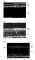
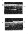
- Figs. 4 to 8 are each an SEM photograph of a cross-section of the array substrate before formation of a counter electrode.
- Figs. 4 and 5 each illustrate the array substrate in the present embodiment.
- Figs. 6 to 8 each illustrate an array substrate in Comparative Embodiments 2 to 4.
- oxygen-based plasma treatment was performed using a plasma CVD device for forming the second interlayer film 20 before formation of the second interlayer insulating film 20.
- the oxygen-based gas used was N 2 O gas.
- the respective array substrates illustrated in Figs. 4 to 8 were produced in the same manner except that the time for plasma treatment, the time from placement of the array substrate in a plasma CVD device to the start of the plasma treatment (hereinafter, also referred to as time before the start of treatment), and the distance between the electrodes in the plasma CVD device were changed.
- the time for plasma treatment and/or the time before the start of treatment was/were prolonged compared to those for the array substrate illustrated in Fig.
- the distance between the electrodes was 30 mm for the array substrate illustrated in Fig. 7 , and was 25 mm for the array substrates illustrated in the drawings other than Fig. 7 .
- the RF power was set to 57 mW/cm 2
- the process pressure was set to 1100 mTorr.
- the height (the amount shaved) of the step portion of the organic insulating film 18 was 10 nm in the array substrate illustrated in Fig. 4 , 20 nm in the array substrate illustrated in Fig. 5 , 30 nm in the array substrate illustrated in Fig. 6 , 100 nm in the array substrate illustrated in Fig. 7 , and 180 nm in the array substrate illustrated in Fig. 8 .
- the results show that when the height of the step portion (the amount of the organic insulating film 18 shaved) was 30 nm or higher, the coverage of the second interlayer insulating film 20 is insufficient, and fissures (cracks) 20a are generated, at portions around the step portions. Such fissures not only allow moisture to enter therethrough but also cause defects such as a decrease in the resist applicability and an alignment disorder of the liquid crystal molecules.
- the results show that when the height of the step portion was 20 nm or lower, favorable coverage without fissures can be achieved.
- the present embodiment is substantially the same as Embodiment 1 except that the structure around the end portions of the counter electrodes is different. Therefore, in the present embodiment, the features of the present embodiment are mainly described, and the features that are the same as those in Embodiment 1 are not described. Also, components (including the portions thereof) having the same or similar functions in the present embodiment and Embodiment 1 are provided with the same reference signs, and the components are not described in the present embodiment.
- Fig. 9 is a schematic cross-sectional view of an array substrate included in the liquid crystal display of Embodiment 2, illustrating a TFT and the neighboring regions thereof in the display region.
- the array substrate 10 included in the liquid crystal display of the present embodiment is provided with the insulating substrate 11, the TFTs 22 arranged on the insulating substrate 11, the first interlayer insulating film 17 arranged on the TFTs 22, the organic insulating film 18 arranged on the first interlayer insulating film 17, the counter electrode 19 arranged on the organic insulating film 18, the second interlayer insulating film 20 covering the organic insulating film 18 and the counter electrode 19, and the pixel electrodes 21 arranged on the second interlayer insulating film 20.
- the TFTs 22 each include the gate electrode 12, the gate insulating film 13, the semiconductor layer 14, the source electrode 15, and the drain electrode 16.
- plasma treatment (preferably oxygen plasma treatment) is performed before formation of the second interlayer insulating film 20.
- the counter electrode 19 therefore has a plasma-treated surface.
- more mild plasma treatment is performed than in the case of Embodiment 1.
- the organic insulating film 18 is hardly etched by the plasma treatment. More specifically, it is preferred to shorten the time for plasma treatment and/or the time before the start of treatment compared to the case of Embodiment 1.
- the RF power, the process pressure, and the distance between electrodes can respectively be set to, for example, 42 mW/cm 2 , 1100 mTorr, and 25 mm.
- the organic insulating film 18 does not have a step portion under the end portion 19a of the counter electrode 19, and has a flat upper surface 18b, as illustrated in Fig. 9 .
- the present embodiment can achieve the same effects as Embodiment 1.
- the pixel electrodes are arranged on the counter electrode with the second interlayer insulating film in between.
- the counter electrode may be arranged on the pixel electrodes with the second interlayer insulating film in between.
- the pixel electrodes correspond to the above-described transparent electrode.
- Embodiments 1 and 2 what is called bottom-gate TFTs were described in which the gate electrodes were arranged between the insulating substrate and the semiconductor layers. In each of the embodiments, however, the TFTs may be of any type appropriately selected. For example, what is called planar TFTs may be used in which semiconductor layers are arranged between the insulating substrate and the gate electrodes, and the source electrodes and the drain electrodes are arranged on the gate electrodes with an interlayer insulating film in between.
- the liquid crystal displays of the respective embodiments may be black and white liquid crystal displays.
- each of the pixels is not necessarily divided into subpixels.
- the display mode for the liquid crystal displays of the respective embodiments may be any appropriate mode that utilizes an organic insulating film, a transparent electrode arranged on the organic insulating film, and an interlayer insulating film arranged on the transparent electrode.
- the display mode may be a twisted nematic (TN) mode, a multi-domain vertical alignment (MVA) mode, an in-plane switching (IPS) mode utilizing the counter electrode and the pixel electrodes each having a comb structure and an interlayer insulating film arranged between the counter electrode and the pixel electrodes, or a transverse bend alignment (TBA) mode.
- TN twisted nematic
- MVA multi-domain vertical alignment
- IPS in-plane switching
- TSA transverse bend alignment
- the liquid crystal layer includes nematic liquid crystal molecules having a negative anisotropy of dielectric constant, the liquid crystal molecules are vertically aligned with no voltage applied, the array substrate includes a pair of electrodes (e.g. counter electrode and pixel electrodes each having a comb structure) and an interlayer insulating film arranged between the pair of electrodes, and the liquid crystal molecules are bend-aligned by the transverse electric field generated between the pair of electrodes.
- the array substrate includes a pair of electrodes (e.g. counter electrode and pixel electrodes each having a comb structure) and an interlayer insulating film arranged between the pair of electrodes, and the liquid crystal molecules are bend-aligned by the transverse electric field generated between the pair of electrodes.
- a suitable display mode for liquid crystal displays is a mode in which the array substrate includes a transparent electrode, transparent pixel electrodes, and an interlayer insulating film between the electrodes (hereinafter, such a structure is also referred to as a transparent Cs structure), and the retention capacitance is formed by these components.
- display modes include continuous pinwheel alignment (CPA) mode which utilizes a transparent Cs structure.
- the liquid crystal layer includes nematic liquid crystal molecules having a negative anisotropy of dielectric constant; the liquid crystal molecules are vertically aligned with no voltage applied, the array substrate includes a transparent electrode, an interlayer insulating film arranged on the transparent electrode, and transparent pixel electrodes arranged on the interlayer insulating film; common signals are supplied to the transparent electrode; the counter substrate includes a transparent electrode facing the pixel electrodes, and dot-like projections (rivets) arranged on the counter electrode; and the liquid crystal molecules are radially aligned with the rivets as the centers by the vertical electric field generated between the pixel electrodes and the counter electrode.
- openings having a circular, cross, or polygonal shape may be formed on the counter electrode, so that the liquid crystal molecules can be radially aligned with the openings as the centers.
- liquid crystal panels of the respective liquid crystal displays may be provided with a reflecting display portion that provides display by reflecting external light.
Landscapes
- Physics & Mathematics (AREA)
- Nonlinear Science (AREA)
- Mathematical Physics (AREA)
- Chemical & Material Sciences (AREA)
- Crystallography & Structural Chemistry (AREA)
- General Physics & Mathematics (AREA)
- Optics & Photonics (AREA)
- Engineering & Computer Science (AREA)
- Microelectronics & Electronic Packaging (AREA)
- Liquid Crystal (AREA)
Abstract
Description
- The present invention relates to a liquid crystal display. More specifically, the present invention relates to a liquid crystal display suitable for a fringe field switching (FFS) mode, which is one of horizontal alignment modes.
- Liquid crystal displays commonly include a thin film transistor substrate (hereinafter, also referred to as an array substrate) on which pixel electrodes and thin-film transistors (TFTs) are formed in a matrix; a counter substrate that faces the array substrate and includes color filters arranged to correspond to the pixel electrodes; and a liquid crystal layer sandwiched between the array substrate and the counter substrate. Liquid crystal displays control the alignment of liquid crystal molecules in the liquid crystal layer to control the transmittance of light for each pixel, thereby producing an image.
- Since liquid crystal displays are flat and lightweight, they can be used in various fields from large-sized display devices (e.g. TVs) to cellphones and digital still cameras (DSCs). Liquid crystal displays, however, sometimes have problems in the viewing angle properties. Poor viewing angle properties change the luminance and/or the chromaticity in the front view and oblique views of the display.
- The known major liquid crystal modes for liquid crystal displays are a vertical alignment (VA) mode which controls the alignment of liquid crystal molecules by applying an electric field in the direction perpendicular to the substrate surfaces to liquid crystal molecules having a negative anisotropy of dielectric constant; and a horizontal alignment mode which controls the alignment of liquid crystal molecules by applying an electric field in the direction horizontal (parallel) to the substrate surfaces (i.e. transverse electric field) to liquid crystal molecules having a positive or negative anisotropy of dielectric constant. In terms of the viewing angle, the horizontal alignment mode is generally considered to be better than the vertical alignment mode. One of the horizontal alignment-mode liquid crystal displays suggested is a fringe field switching (FFS)-mode liquid crystal display. FFS-mode liquid crystal displays provide display by applying a fringe electric field (oblique electric field including both the transverse electric field components and vertical electric field components) to the liquid crystal layer.
- As to the FFS-mode liquid crystal displays,
Patent Literature 1, for example, discloses a technology for forming an overhanging portion by shaving the surface of an organic passivation film by plasma-asher treatment before formation of an interlayer insulating film on the counter substrate formed on the organic passivation film. - Patent Literature 1:
JP 2012-53371 A - In an FFS-mode liquid crystal display, the adhesion between the counter electrode and the interlayer insulating film formed on the counter electrode may decrease to cause the interlayer insulating film to peel. This problem occurs probably because of the following two factors. One of the factors is that the film forming temperature for an interlayer insulating film cannot be raised because the interlayer insulating film needs to be formed on the organic insulating film, and thus the interlayer insulating film is formed at low temperatures. The other factor is the resist residues on the counter electrode. The above-described factors are regarded as bringing difficulties in providing cohesion between the counter electrode and the interlayer insulating film.
-
Fig. 10 is a schematic cross-sectional view of an array substrate inComparative Embodiment 1, illustrating a TFT and the neighboring regions thereof in a display region, on which the present inventors have made studies. - The array substrate of
Comparative Embodiment 1 is an array substrate for FFS-mode liquid crystal displays. As illustrated inFig. 10 , the array substrate is provided with aninsulating substrate 111,TFTs 122 arranged on theinsulating substrate 111, a firstinterlayer insulating film 117 arranged on theTFTs 122, an organicinsulating film 118 arranged on the firstinterlayer insulating film 117, acounter electrode 119 arranged on the organicinsulating film 118, a secondinterlayer insulating film 120 covering the organicinsulating film 118 and thecounter electrode 119, andpixel electrodes 121 arranged on the secondinsulating film 120. TheTFTs 122 each include agate electrode 112, agate insulating film 113, asemiconductor layer 114, asource electrode 115, and adrain electrode 116. - The organic
insulating film 118 is arranged to reduce the irregularities on the surface of the array substrate. In the case of forming the secondinterlayer insulating film 120 by plasma-enhanced chemical vapor deposition (CVD), a higher film formation temperature gives higher adhesion to the base film. The film formation temperature, however, needs to be low in order to suppress changes in the properties of the organicinsulating film 118. Specifically, the film formation temperature is preferably 220°C or lower. Here, the secondinterlayer insulating film 120 formed at low temperatures unfortunately has poor adhesion to the base film, and may peel off the base film as described above. -
Patent Literature 1 deals with the problem by a technology of enhancing the adhesion between the counter electrode and the interlayer insulating film by performing plasma-asher treatment before formation of the interlayer insulating film so as to shave the surface of the organic passivation film and also roughen the counter electrode surface, and removing the resist residues on the counter electrode. - With the technology described in
Patent Literature 1, however, the plasma-asher treatment greatly shaves the organic passivation film, and the counter electrode on the organic passivation film overhangs on the organic passivation film. Therefore, the film coatability of the interlayer insulating film arranged on the counter electrode deteriorates in the vicinity of an end portion of the counter electrode, causing defects. Specifically, the moisture resistance of the interlayer insulating film may decrease or the alignment disorder of the liquid crystal molecules may occur. Also, the deterioration in the coatability may decrease the resist applicability of the film during photolithography for forming openings in the interlayer insulating film. As a result, application defects such as cissing may occur when a resist material is applied to the interlayer insulating film. - The present invention has been made in view of the above current state of the art, and aims to provide a liquid crystal display capable of enhancing moisture resistance and resist applicability while suppressing alignment disorder of liquid crystal molecules.
- One aspect of the present invention may be a liquid crystal display including:
- an organic insulating film;
- a transparent electrode arranged on the organic insulating film; and
- an interlayer insulating film arranged on the transparent electrode,
- the transparent electrode including a plasma-treated surface,
- the organic insulating film being shaved vertically from an end portion of the transparent electrode, and thereby including a step portion under the end portion,
- the transparent electrode not laterally protruding from the step portion,
- the step portion having a height of 20 nm or lower.
- Hereinafter, such a liquid crystal display is also referred to as a first liquid crystal display of the present invention.
- Another aspect of the present invention may be a liquid crystal display including:
- an organic insulating film;
- a transparent electrode arranged on the organic insulating film; and
- an interlayer insulation film arranged on the transparent electrode,
- the transparent electrode including a plasma-treated surface,
- the organic insulating film including a flat upper surface without a step portion under an end portion of the transparent electrode.
- Hereinafter, such a liquid crystal display is also referred to as a second liquid crystal display of the present invention.
- The preferred embodiments of the first and second liquid crystal displays of the present invention are described below. The following preferred embodiments may be appropriately combined with one another, and an embodiment obtained by combining at least two of the following preferred embodiments is also one preferred embodiment.
- The step portion may have a height lower than 10 nm.
- The transparent electrode may be a counter electrode or a pixel electrode.
- The first and second liquid crystal displays of the present invention may each further include a TFT including an oxide semiconductor under the organic insulating film.
- The oxide semiconductor may contain indium, gallium, zinc, and oxygen.
- The present invention can provide a liquid crystal display capable of enhancing moisture resistance and resist applicability while suppressing alignment disorder of liquid crystal molecules.
-
-
Fig. 1 is a schematic cross-sectional view of a liquid crystal display ofEmbodiment 1, illustrating a TFT in a display region and the neighboring regions thereof. -
Fig. 2 is an enlarged view of the vicinity of an end portion of a counter substrate inFig. 1 . -
Fig. 3 is a process flow chart of an array substrate included in the liquid crystal display ofEmbodiment 1. -
Fig. 4 is an SEM photograph of a cross-section of the array substrate ofEmbodiment 1 before formation of a counter electrode. -
Fig. 5 is another SEM photograph of a cross-section of the array substrate ofEmbodiment 1 before formation of a counter electrode. -
Fig. 6 is an SEM photograph of a cross-section of an array substrate of Comparative Embodiment 2 before formation of a counter electrode. -
Fig. 7 is an SEM photograph of a cross-section of an array substrate of Comparative Embodiment 3 before formation of a counter electrode. -
Fig. 8 is an SEM photograph of a cross-section of an array substrate of Comparative Embodiment 4 before formation of a counter electrode. -
Fig. 9 is a schematic cross-sectional view of an array substrate included in the liquid crystal display of Embodiment 2, illustrating a TFT and the neighboring regions thereof in a display region. -
Fig. 10 is a schematic cross-sectional view of an array substrate ofComparative Embodiment 1, illustrating a TFT and the neighboring regions thereof in a display region. - The present invention will be described in more detail below with reference to the drawings based on embodiments which, however, are not intended to limit the scope of the present invention.
- The end portion of a counter electrode herein means a portion at which the counter electrode ends. The end portion of a counter electrode therefore may be a portion adjacent to an opening formed in the counter electrode or a portion (peripheral portion) adjacent to the periphery of the counter electrode, for example.
-
Fig. 1 is a schematic cross-sectional view of a liquid crystal display ofEmbodiment 1, illustrating a TFT and the neighboring regions thereof in a display region. - The liquid crystal display of the present embodiment is an active-matrix driven, transparent, FFS-mode (one of horizontal alignment modes) liquid crystal display. As illustrated in
Fig. 1 , the liquid crystal display of the present embodiment is provided with aliquid crystal panel 1, a backlight (not illustrated) arranged on the rear side of theliquid crystal panel 1, a controller (not illustrated) configured to drive and control theliquid crystal panel 1 and the backlight, and a flexible substrate (not illustrated) connecting theliquid crystal panel 1 to the controller. - The
liquid crystal panel 1 includes a display region for display of images. The display region includes pixels arranged in a matrix. Each pixel may include subpixels in multiple colors (e.g. three colors: red, green, and blue). The liquid crystal display of the present embodiment may be a black and white liquid crystal display, and in this case, it is not necessary to divide each pixel into multiple subpixels. - The
liquid crystal panel 1 includes an array substrate (active matrix substrate) 10, acounter substrate 40 which faces thearray substrate 10, aliquid crystal layer 30 and a seal (not shown) arranged between thesubstrates alignment film 31 arranged on theliquid crystal layer 30 side surface of thearray substrate 10, analignment film 32 arranged on theliquid crystal layer 30 side surface of thecounter substrate 40, a source driver (not illustrated) which is a driving circuit for the later-described source bus lines, and a gate driver (not illustrated) which is a driving circuit for the later-described gate bus lines. Thealignment films liquid crystal layer 30. - The seal is formed to surround the display region. The seal bonds the
substrates liquid crystal layer 30 between thesubstrates - The
array substrate 10 is arranged on the rear side of the liquid crystal display, while thecounter substrate 40 is arranged on the viewer side. Thearray substrate 10 is irradiated with light from the backlight, and an image displayed on theliquid crystal panel 1 is viewed from thecounter substrate 40 side. To the surface on the side opposite to theliquid crystal layer 30 side of each of thesubstrates - The
counter substrate 40 includes a transparent insulatingsubstrate 41,color filters 42 in multiple colors, a black matrix (BM) 43 configured to function as a light-shielding member, anovercoat film 44 covering thecolor filters 42 and theBM 43, multiple pillar-shaped spacers (not illustrated), and an externalconductive film 45 arranged on the surface opposite to theliquid crystal layer 30 side surface of thecounter substrate 40. TheBM 43 is formed to shield from light the regions (frame regions) surrounding the display region, the regions facing the bus lines, and the regions facing the later-described TFTs. The color filters 42 in the respective colors are arranged in the display region, and are formed to cover the regions defined by theBM 43, i.e., the openings of theBM 43. Theovercoat film 44 is formed to reduce irregularities on the surface (flatter the surface) of thecounter substrate 40. The pillar-shaped spacers are components arranged to keep a given space between thearray substrate 10 and thecounter substrate 40, and are arranged within the light-shielding region on theBM 43. The externalconductive film 45 is arranged to stabilize the electric field inside theliquid crystal panel 1, and is formed from a transparent conductive film material such as indium tin oxide (ITO) by sputtering, for example. - The
array substrate 10 includes a transparent insulatingsubstrate 11, and various components formed on the insulatingsubstrate 11. Specifically, thearray substrate 10 includes the source bus lines and gate bus lines (neither of which is illustrated) arranged to cross one another, in the display region. Multiple common bus lines may be formed in parallel with the gate bus lines. The subpixels almost conform to the respective regions defined by the source bus lines and the gate bus lines or common bus lines. - The
array substrate 10 includesmultiple TFTs 22 configured to function as switching elements in the display region. On the insulatingsubstrate 11, agate electrode 12 is formed, and agate insulating film 13 is arranged to cover thegate electrode 12. On thegate insulating film 13, asemiconductor layer 14 is formed to overlap thegate electrode 12. Thesemiconductor layer 14 has an island shape. On thegate insulating film 13, asource electrode 15 and adrain electrode 16 are formed to partially overlap thesemiconductor layer 14. On thegate insulating film 13, thesemiconductor layer 14, thesource electrode 15, and thedrain electrode 16, a firstinterlayer insulating film 17 is provided. On the firstinterlayer insulating film 17, an organic insulatingfilm 18 is provided. On the organic insulatingfilm 18, atransparent counter electrode 19 corresponding to the transparent electrode is provided. On thecounter electrode 19, a secondinterlayer insulating film 20 is arranged to cover the organic insulatingfilm 18 and thecounter electrode 19. On the secondinterlayer insulating film 20,transparent pixel electrodes 21 connected to therespective TFTs 22 are arranged. TheTFTs 22 and thepixel electrodes 21 are formed in regions corresponding to the respective subpixels. Each of theTFTs 22 is connected to the corresponding source bus line and gate bus line. - Each of the
TFTs 22 has a bottom gate structure, and formed from thegate electrode 12, thegate insulating film 13, thesemiconductor layer 14, thesource electrode 15, and thedrain electrode 16. Thegate electrode 12 is connected to a gate bus line, and thesource electrode 15 is connected to the source bus line. Thesource electrode 15 and thedrain electrode 16 are each connected to thesemiconductor layer 14. - On the
drain electrode 16, the firstinterlayer insulating film 17, the organic insulatingfilm 18, and the secondinterlayer insulating film 20 each have an opening, and thepixel electrode 21 is connected to thedrain electrode 16 through these openings. On each of thepixel electrodes 21, multiple slits (elongated openings) 21a parallel to one another are formed. Thecounter electrode 19 is formed to face at least theslits 21a in the region excluding the openings. Thecounter electrode 19 may be formed to cover the entire display region in the regions excluding the openings. - To the gate bus lines and the
gate electrode 12, pulse scanning signals are supplied at certain timings from the gate driver, and the scanning signals are line-sequentially applied to therespective TFTs 22. TheTFTs 22 are each turned on for a given period of time upon input of a scanning signal. While theTFTs 22 are turned on, image signals are supplied to thepixel electrodes 21 from the source driver through the source bus lines and theTFTs 22. To thecounter electrode 19, a common signal is supplied which is a signal applied commonly to all the pixels. Therefore, when an image signal is applied to one of thepixel electrodes 21, a parabolic electric line of force will be generated between thepixel electrode 21 and thecounter electrode 19, which produces a fringe electric field corresponding to the image signal in theliquid crystal layer 30. The fringe electric field controls the alignment (rotation) of liquid crystal molecules (typically, nematic liquid crystal molecules with a positive anisotropy of dielectric constant), whereby the light transmittance of each subpixel is controlled. In this manner, a large number of subpixels are each independently driven, so that an image is displayed in the display region. - The
pixel electrodes 21 are placed on thecounter electrode 19, with the secondinterlayer insulating film 20 in between. To thecounter electrode 19, common signals are applied as described above. Therefore, when an image signal is applied to thepixel electrodes 21, these transparent components form retention capacitance. In this manner, thepixel electrodes 21 and thecounter electrode 19 are also configured to function as electrodes for retention capacitance. The secondinterlayer insulating film 20 is also configured to function as an insulator that provides insulation between thepixel electrodes 21 and thecounter electrode 19, and to function also as a dielectric body that forms retention capacitance. -
Fig. 2 is an enlarged view of the vicinity of an end portion of the counter electrode illustrated inFig. 1 . - As described later, plasma treatment is performed before formation of the second
interlayer insulating film 20 in the present embodiment. Therefore, thecounter electrode 19 has a plasma-treated surface. Also, the plasma treatment slightly etches a part of the organic insulatingfilm 18. As a result, as illustrated inFig. 2 , the organic insulatingfilm 18 will be perpendicularly shaved from anend portion 19a of thecounter electrode 19, and thus has astep portion 18a under theend portion 19a. Thecounter electrode 19, however, does not protrude laterally from thestep portion 18a, and therefore an overhanging portion is not formed. The height h of thestep portion 18a, i.e., the amount of the organic insulatingfilm 18 shaved perpendicularly, is set to 20 nm or lower. Here, the expression "perpendicularly" means the normal direction from the main surfaces of the insulatingsubstrate 11. - With such a structure, it is possible to achieve adhesion of the second
interlayer insulating film 20 by the plasma treatment, and also achieve the coatability of the secondinterlayer insulating film 20 in the vicinity of theend portion 19a and thestep portion 18a. The secondinterlayer insulating film 20, functioning as a dielectric body for retention capacitance as described above, also functions to block moisture. Hence, if the coatability of the film in the vicinity of thestep portion 18 deteriorates, moisture may enter the organic insulatingfilm 18 from thestep portion 18a to swell the organic insulatingfilm 18, deteriorating the properties of the organic insulatingfilm 18. Moisture in this case from thestep portion 18a may reach theTFTs 22 to deteriorate the properties of theTFTs 22. The present embodiment can suppress generation of such defects. - Since the second
interlayer insulating film 20 has sufficient coatability, the resist applicability of the secondinterlayer insulating film 20 can be prevented from decreasing. Therefore, generation of application defects such as cissing can be suppressed when the resist material is applied to the secondinterlayer insulating film 20. - The above structure can suppress generation of alignment disorder of the liquid crystal molecules in the vicinity of the
end portion 19a and thestep portion 18a. - Here, the height h of the
step portion 18a may be lower than 10 nm. The lower limit for the height h is not particularly limited, and may be appropriately set. The height h may be, for example, 1 nm or higher. - Hereinafter, the method for producing a liquid crystal display of the present embodiment is described.
Fig. 3 is a process flow chart of an array substrate included in the liquid crystal display ofEmbodiment 1. - First, the insulating
substrate 11 having an insulating surface is prepared. The insulatingsubstrate 11 can be any insulating substrate commonly used for displays, such as a glass substrate, a silicon substrate, and a heat-resistant plastic substrate. Examples of the material of the plastic substrate include polyethylene terephthalate resin, polyethylenenaphthalate resin, polyether sulfone resin, acrylic resin, and polyimide resin. - Next, a conductive layer (hereinafter, also referred to as a gate layer) including components such as the
gate electrodes 12 and gate bus lines is formed on the insulatingsubstrate 11. The material of the gate layer can be, for example, molybdenum (Mo) or aluminum (Al). Also, the gate layer may include a barrier metal layer, the material of which can be, for example, titanium (Ti) or molybdenum (Mo). The gate layer is formed by sputtering, and patterned by wet etching or dry etching through a resist pattern formed thereon by photolithography. - Next, the
gate insulating film 13 is formed on the insulatingsubstrate 11 on which the gate layer is formed. The material of thegate insulating film 13 can be, for example, silicon nitride (SiNx) or silicon oxide (e.g. SiO2). Thegate insulating film 13 is formed by plasma CVD or sputtering. Thegate insulating film 13 may be a laminate formed from the above materials. - Next, the island-shaped semiconductor layers 14 are formed on the
gate insulating film 13. The material of the semiconductor layers 14 can be, for example, amorphous silicon (a-Si), polysilicon (poly-Si), or an oxide semiconductor. The semiconductor layers 14 are formed by plasma CVD or sputtering, and are patterned by wet etching or dry etching through a resist pattern formed by photolithography. - The oxide semiconductor preferably contains oxygen (O) and at least one element selected from the group consisting of indium (In), gallium (Ga), aluminum (Al), copper (Cu), zinc (Zn), magnesium (Mg), and cadmium (Cd), and more preferably contains indium (In), gallium (Ga), zinc (Zn), and oxygen (O). The mobility of the
TFTs 22 in the case of using an oxide semiconductor can be made higher than that in the case of using amorphous silicon. Therefore, even when the definition is increased, that is, even when the turned-on time of theTFT 22 per subpixel is shortened, the voltage can be sufficiently applied to theliquid crystal layer 30. Also, when an oxide semiconductor is used, leakage current with theTFTs 22 turned off can be reduced compared to the case of using amorphous silicon. Driving modes, such as low frequency driving and driving with stop periods, can therefore be employed regardless of whether the definition is high or not, and thereby the power consumption can be reduced. - Next, on the insulating
substrate 11 on which the semiconductor layers 14 are formed, a conductive layer (hereinafter, also referred to as a source layer) including thesource electrodes 15, thedrain electrodes 16, and the source bus lines is formed. The material of the source layer can be, for example, molybdenum (Mo) or aluminum (Al). Also, the source layer may include a barrier metal layer, the material of which can be, for example, titanium (Ti) or molybdenum (Mo). The source layer is formed by sputtering, and patterned by wet etching or dry etching through a resist pattern formed thereon by photolithography. - Next, the first
interlayer insulating film 17 as an inorganic passivation film is formed on the insulatingsubstrate 11 on which the source layer is formed. The firstinterlayer insulating film 17 protectsTFTs 22, especially channels of theTFTs 22, from impurities. The material of the firstinterlayer insulating film 17 can be, for example, silicon nitride (SiNx) or silicon oxide (e.g. SiO2). The firstinterlayer insulating film 17 is formed by plasma CVD or sputtering. The firstinterlayer insulating film 17 may be a laminate formed from the above materials. - Next, the organic insulating
film 18 is formed on the firstinterlayer insulating film 17. Openings for connecting thepixel electrodes 21 to thedrain electrodes 16 are formed in the organic insulatingfilm 18. The organic insulatingfilm 18 is formed to protect theTFTs 22 and reduce irregularities on the surface (flatter the surface) of thecounter substrate 40. The thickness of the organic insulatingfilm 18 is preferably 1 µm to 4 µm, and more preferably 2 µm to 3 µm. The material of the organic insulatingfilm 18 can be a photosensitive resin such as an acrylic photosensitive resin, a silicon-based photosensitive resin, and a polyimide-based photosensitive resin. In the case of using a photosensitive resin material, exposure and development of the photosensitive resin film, i.e. patterning of the film, can be performed without forming a resist pattern. After the patterning, the patterned film is fired by annealing. The annealing provides a smooth, curved surface to the organic insulatingfilm 18 at portions around the openings. The annealing is preferably performed at 190°C to 230°C, more preferably at 200°C to 220°C, for preferably 30 minutes to 2 hours, more preferably about 1 hour. - Then, the first
interlayer insulating film 17 is etched by dry etching with the organic insulatingfilm 18 as a mask, so that the surfaces of thedrain electrodes 16 are exposed. As a result, contact holes penetrating the organic insulatingfilm 18 and the firstinterlayer insulating film 17 are formed. - Next, the
counter electrode 19 is formed on the organic insulatingfilm 18. Thecounter electrode 19 is formed on the flat upper surface of the organic insulatingfilm 18. The material of thecounter electrode 19 can be, for example, a transparent conductive film material. Specific examples of the transparent conductive film material include metal oxides such as ITO. Thecounter electrode 19 is formed by sputtering, and patterned by wet etching or dry etching through a resist pattern formed by photolithography. The thickness of thecounter electrode 19 is preferably 50 nm to 200 nm, and more preferably 60 nm to 120 nm. - Next, before formation of the second
interlayer insulating film 20, treatment (hereinafter, also referred to as pretreatment) is performed on the insulatingsubstrate 11 on which thecounter electrode 19 is formed. The pretreatment may be plasma treatment. Thereby, the resist residue on thecounter electrode 19 can be removed. The pretreatment can also roughen the surfaces of thecounter electrode 19 and the organic insulatingfilm 18. As a result, the adhesion between thecounter electrode 19 and the secondinterlayer insulating film 20 and between the organic insulatingfilm 18 and the secondinterlayer insulating film 20 can be enhanced. Also, since plasma has a strong influence particularly on the organic insulatingfilm 18, the exposed portion of the organic insulatingfilm 18 is removed by decomposition by the plasma. That is, the plasma treatment etches the organic insulatingfilm 18 with thecounter electrode 19 as a mask. As a result, thestep portion 18a having a height of 20 nm or lower is formed as described above. - However, the overhanging portion as disclosed in
Patent Literature 1 can be formed depending on the plasma treatment conditions, and it is therefore preferred to appropriately adjust the plasma treatment conditions. The plasma treatment may be performed by any device by any method. Examples of the device include a plasma CVD device, a plasma etching device, and plasma ashing device. In particular, the plasma treatment is preferably performed in the same device as the device for forming the second interlayer insulating film 20 (plasma CVD device is suitable). When a plasma CVD device is used, the organic insulatingfilm 18 is considered to be etched (removed by decomposition) isotropically. However, since the height of thestep portion 18a is set to 20 nm or lower in the present embodiment, formation of an overhanging portion can be prevented. - The amount of the organic insulating
film 18 shaved increases as the plasma treatment time increases. The treatment time is thus preferably as short as possible. When a plasma CVD device for forming the secondinterlayer insulating film 20 is used, the temperature in the device is around 200°C which is higher than the ordinary temperature as described below. Hence, the plasma treatment is preferably started before the temperature of the insulatingsubstrate 11 excessively increases after the insulatingsubstrate 11 is placed in the plasma CVD device. The amount of the organic insulatingfilm 18 shaved increases as the time before the start of treatment increases. Accordingly, the time for plasma treatment and the time before the start of plasma treatment are both preferably set to several seconds to tens of seconds. - The plasma treatment is preferably oxygen-based plasma treatment utilizing oxygen-based gases. Specific suitable examples of the oxygen-based gases include oxygen (O2) and nitrous oxide (N2O). N2O gas can be used in the case of a plasma CVD device, and O2 gas can be used in the case of a plasma etching device or a plasma ashing device. If the
counter electrode 19 is formed using a metal oxide, the surface of thecounter electrode 19 can be refined by oxygen-based plasma treatment, and oxygen deficiency on the surface can be repaired. - Next, on the insulating
substrate 11 on which the pretreatment has been performed, the secondinterlayer insulating film 20 as an inorganic passivation film is formed. The material of the secondinterlayer insulating film 20 can be, for example, silicon nitride (SiNx) or silicon oxide (e.g. SiO2). The secondinterlayer insulating film 20 is formed by the plasma CVD method, and patterned by wet etching or dry etching through a resist pattern formed by photolithography. As a result, openings are formed in the second interlayer insulating film. These openings are formed such that they at least partially overlap the contact holes, that is, thedrain electrodes 16 are exposed in the openings. The secondinterlayer insulating film 20 may be a laminate film formed from the above materials. - The temperature for forming the second
interlayer insulating film 20 is limited to the range that does not cause deterioration of the organic insulatingfilm 18. Specifically, the temperature is preferably equal to or lower than the firing temperature for the organic insulatingfilm 18. More specifically, the temperature is preferably 190°C to 230°C, more preferably 200°C to 220°C. Thus, since the secondinterlayer insulating film 20 is formed by what is called a low-temperature CVD method, a decrease in the cohesion (adhesion) between the secondinterlayer insulating film 20 and thecounter electrode 19 and the organic insulatingfilm 18, which are formed under the secondinterlayer insulating film 20, is concerned. However, since the above pretreatment has been performed before formation of the secondinterlayer insulating film 20, the cohesion (adhesion) can be sufficiently achieved. The present inventors have verified that in the present embodiment, an overhanging portion is not formed by theend portion 19a of thecounter electrode 19, and that the above-described cohesion is sufficiently achieved. - Next, the
pixel electrodes 21 are formed on the insulatingsubstrate 11 on which the secondinterlayer insulating film 20 is formed. The material of thepixel electrodes 21 can be, for example, a transparent conductive material. Specific examples of the transparent conductive film material include metal oxides such as ITO. The pixel electrodes are formed by sputtering, and patterned by wet etching or dry etching through a resist pattern formed by photolithography. - As a result, an array substrate is completed. In the following cell assembling step, an alignment film is formed by application of an alignment film material containing an organic resin such as polyimide to the surfaces of the array substrate and the separately produced counter substrate. By a method such as rubbing treatment and photoalignment treatment, the respective alignment films are subjected to alignment treatment such that the liquid crystal molecules are aligned in a given direction.
- Next, a sealing material is applied to one of the array substrate and the counter substrate, so that the display region is surrounded by the sealing material. On one of the array substrate and the counter substrate, a liquid crystal material is dropped. The array substrate and the counter substrate are then placed on the top of the other such that the alignment films on the respective substrates face one another. The sealing material is then cured to bond the substrates. Thereby, a liquid crystal layer is formed between the substrates.
- Then, a liquid crystal panel is completed through the step of bonding the polarizing plate and optionally a phase plate. To the liquid crystal panel, an FPC substrate and (optionally) an IC chip on which a driving circuit is formed are connected, and the controller and the backlight unit are mounted on the liquid crystal panel. The liquid crystal panel is then housed in a case, whereby a liquid crystal display of
Embodiment 1 is completed. - The following shows the results of studying the relation between the height h of the
step portion 18a of the organic insulatingfilm 18 and the coatability of the secondinterlayer insulating film 20.Figs. 4 to 8 are each an SEM photograph of a cross-section of the array substrate before formation of a counter electrode.Figs. 4 and 5 each illustrate the array substrate in the present embodiment.Figs. 6 to 8 each illustrate an array substrate in Comparative Embodiments 2 to 4. - In each of these steps for producing an array substrate, oxygen-based plasma treatment was performed using a plasma CVD device for forming the
second interlayer film 20 before formation of the secondinterlayer insulating film 20. The oxygen-based gas used was N2O gas. The respective array substrates illustrated inFigs. 4 to 8 were produced in the same manner except that the time for plasma treatment, the time from placement of the array substrate in a plasma CVD device to the start of the plasma treatment (hereinafter, also referred to as time before the start of treatment), and the distance between the electrodes in the plasma CVD device were changed. For the array substrates illustrated inFigs. 5 to 8 , the time for plasma treatment and/or the time before the start of treatment was/were prolonged compared to those for the array substrate illustrated inFig. 4 . The distance between the electrodes was 30 mm for the array substrate illustrated inFig. 7 , and was 25 mm for the array substrates illustrated in the drawings other thanFig. 7 . For each of the array substrates illustrated inFigs. 4 to 8 , the RF power was set to 57 mW/cm2, and the process pressure was set to 1100 mTorr. - As a result, the height (the amount shaved) of the step portion of the organic insulating
film 18 was 10 nm in the array substrate illustrated inFig. 4 , 20 nm in the array substrate illustrated inFig. 5 , 30 nm in the array substrate illustrated inFig. 6 , 100 nm in the array substrate illustrated inFig. 7 , and 180 nm in the array substrate illustrated inFig. 8 . - Also, the results show that when the height of the step portion (the amount of the organic insulating
film 18 shaved) was 30 nm or higher, the coverage of the secondinterlayer insulating film 20 is insufficient, and fissures (cracks) 20a are generated, at portions around the step portions. Such fissures not only allow moisture to enter therethrough but also cause defects such as a decrease in the resist applicability and an alignment disorder of the liquid crystal molecules. - Meanwhile, the results show that when the height of the step portion was 20 nm or lower, favorable coverage without fissures can be achieved.
- The present embodiment is substantially the same as
Embodiment 1 except that the structure around the end portions of the counter electrodes is different. Therefore, in the present embodiment, the features of the present embodiment are mainly described, and the features that are the same as those inEmbodiment 1 are not described. Also, components (including the portions thereof) having the same or similar functions in the present embodiment andEmbodiment 1 are provided with the same reference signs, and the components are not described in the present embodiment. -
Fig. 9 is a schematic cross-sectional view of an array substrate included in the liquid crystal display of Embodiment 2, illustrating a TFT and the neighboring regions thereof in the display region. - The
array substrate 10 included in the liquid crystal display of the present embodiment is provided with the insulatingsubstrate 11, theTFTs 22 arranged on the insulatingsubstrate 11, the firstinterlayer insulating film 17 arranged on theTFTs 22, the organic insulatingfilm 18 arranged on the firstinterlayer insulating film 17, thecounter electrode 19 arranged on the organic insulatingfilm 18, the secondinterlayer insulating film 20 covering the organic insulatingfilm 18 and thecounter electrode 19, and thepixel electrodes 21 arranged on the secondinterlayer insulating film 20. TheTFTs 22 each include thegate electrode 12, thegate insulating film 13, thesemiconductor layer 14, thesource electrode 15, and thedrain electrode 16. - Also in the present embodiment, plasma treatment (preferably oxygen plasma treatment) is performed before formation of the second
interlayer insulating film 20. Thecounter electrode 19 therefore has a plasma-treated surface. In the present embodiment, however, more mild plasma treatment is performed than in the case ofEmbodiment 1. Hence, the organic insulatingfilm 18 is hardly etched by the plasma treatment. More specifically, it is preferred to shorten the time for plasma treatment and/or the time before the start of treatment compared to the case ofEmbodiment 1. When a plasma CVD device is used, the RF power, the process pressure, and the distance between electrodes can respectively be set to, for example, 42 mW/cm2, 1100 mTorr, and 25 mm. As a result, the organic insulatingfilm 18 does not have a step portion under theend portion 19a of thecounter electrode 19, and has a flatupper surface 18b, as illustrated inFig. 9 . - The present embodiment can achieve the same effects as
Embodiment 1. - As described above, in the structure in each of
Embodiments 1 and 2, the pixel electrodes are arranged on the counter electrode with the second interlayer insulating film in between. In the structure in each of the embodiments, the counter electrode may be arranged on the pixel electrodes with the second interlayer insulating film in between. In this case, the pixel electrodes correspond to the above-described transparent electrode. - Also in
Embodiments 1 and 2, what is called bottom-gate TFTs were described in which the gate electrodes were arranged between the insulating substrate and the semiconductor layers. In each of the embodiments, however, the TFTs may be of any type appropriately selected. For example, what is called planar TFTs may be used in which semiconductor layers are arranged between the insulating substrate and the gate electrodes, and the source electrodes and the drain electrodes are arranged on the gate electrodes with an interlayer insulating film in between. - The liquid crystal displays of the respective embodiments may be black and white liquid crystal displays. In this case, each of the pixels is not necessarily divided into subpixels.
- In
Embodiments 1 and 2, FFS-mode liquid crystal displays were described. The display mode for the liquid crystal displays of the respective embodiments may be any appropriate mode that utilizes an organic insulating film, a transparent electrode arranged on the organic insulating film, and an interlayer insulating film arranged on the transparent electrode. For example, the display mode may be a twisted nematic (TN) mode, a multi-domain vertical alignment (MVA) mode, an in-plane switching (IPS) mode utilizing the counter electrode and the pixel electrodes each having a comb structure and an interlayer insulating film arranged between the counter electrode and the pixel electrodes, or a transverse bend alignment (TBA) mode. In the TBA mode, the liquid crystal layer includes nematic liquid crystal molecules having a negative anisotropy of dielectric constant, the liquid crystal molecules are vertically aligned with no voltage applied, the array substrate includes a pair of electrodes (e.g. counter electrode and pixel electrodes each having a comb structure) and an interlayer insulating film arranged between the pair of electrodes, and the liquid crystal molecules are bend-aligned by the transverse electric field generated between the pair of electrodes. In particular, a suitable display mode for liquid crystal displays is a mode in which the array substrate includes a transparent electrode, transparent pixel electrodes, and an interlayer insulating film between the electrodes (hereinafter, such a structure is also referred to as a transparent Cs structure), and the retention capacitance is formed by these components. Examples of such display modes include continuous pinwheel alignment (CPA) mode which utilizes a transparent Cs structure. In the CPA mode utilizing a transparent Cs structure, the liquid crystal layer includes nematic liquid crystal molecules having a negative anisotropy of dielectric constant; the liquid crystal molecules are vertically aligned with no voltage applied, the array substrate includes a transparent electrode, an interlayer insulating film arranged on the transparent electrode, and transparent pixel electrodes arranged on the interlayer insulating film; common signals are supplied to the transparent electrode; the counter substrate includes a transparent electrode facing the pixel electrodes, and dot-like projections (rivets) arranged on the counter electrode; and the liquid crystal molecules are radially aligned with the rivets as the centers by the vertical electric field generated between the pixel electrodes and the counter electrode. Here, in place of forming dot-like projections (rivets), openings having a circular, cross, or polygonal shape, for example, may be formed on the counter electrode, so that the liquid crystal molecules can be radially aligned with the openings as the centers. - Also, in
Embodiments 1 and 2, transparent liquid crystal displays have been described, but the liquid crystal panels of the respective liquid crystal displays may be provided with a reflecting display portion that provides display by reflecting external light. - The above embodiments may be appropriately combined as long as the combination does not go beyond the scope of the present invention. Also, the alternative examples of each embodiment can be combined with the other embodiments.
-
- 1: Liquid crystal panel
- 10: Array substrate
- 11: Insulating substrate
- 12: Gate electrode
- 13: Gate insulating film
- 14: Semiconductor layer
- 15: Source electrode
- 16: Drain electrode
- 17: First interlayer insulating film
- 18: Organic insulating film
- 18a: Step portion
- 18b: Upper surface
- 19: Counter electrode
- 19a: End portion
- 20: Second interlayer insulating film
- 20a: Fissure (crack)
- 21: Pixel electrode
- 21a: Slit
- 22: TFT
- 30: Liquid crystal layer
- 31, 32: Alignment film
- 40: Counter substrate
- 41: Insulating substrate
- 42: Color filter
- 43: Black matrix (BM)
- 44: Overcoat film
- 45: External conductive film
- h: Height of step portion
Claims (6)
- A liquid crystal display comprising:an organic insulating film;a transparent electrode arranged on the organic insulating film; andan interlayer insulating film arranged on the transparent electrode,the transparent electrode comprising a plasma-treated surface,the organic insulating film being shaved vertically from an end portion of the transparent electrode, and thereby including a step portion under the end portion,the transparent electrode not laterally protruding from the step portion,the step portion having a height of 20 nm or lower.
- The liquid crystal display according to claim 1,wherein the step portion has a height lower than 10 nm.
- The liquid crystal display according to claim 1 or 2,
wherein the transparent electrode is a counter electrode or a pixel electrode. - The liquid crystal display according to any one of claims 1 to 3, further comprising
a TFT comprising an oxide semiconductor under the organic insulating film. - The liquid crystal display according to claim 4,
wherein the oxide semiconductor contains indium, gallium, zinc, and oxygen. - A liquid crystal display comprising:an organic insulating film;a transparent electrode arranged on the organic insulating film; andan interlayer insulation film arranged on the transparent electrode,the transparent electrode comprising a plasma-treated surface,the organic insulating film comprising a flat upper surface without a step portion under an end portion of the transparent electrode.
Applications Claiming Priority (2)
| Application Number | Priority Date | Filing Date | Title |
|---|---|---|---|
| JP2012208687 | 2012-09-21 | ||
| PCT/JP2013/074804 WO2014046025A1 (en) | 2012-09-21 | 2013-09-13 | Liquid crystal display |
Publications (2)
| Publication Number | Publication Date |
|---|---|
| EP2899588A1 true EP2899588A1 (en) | 2015-07-29 |
| EP2899588A4 EP2899588A4 (en) | 2015-09-30 |
Family
ID=50341338
Family Applications (1)
| Application Number | Title | Priority Date | Filing Date |
|---|---|---|---|
| EP13838335.1A Withdrawn EP2899588A4 (en) | 2012-09-21 | 2013-09-13 | LIQUID CRYSTAL DISPLAY DEVICE |
Country Status (6)
| Country | Link |
|---|---|
| US (1) | US20150228675A1 (en) |
| EP (1) | EP2899588A4 (en) |
| JP (1) | JPWO2014046025A1 (en) |
| KR (1) | KR20150041792A (en) |
| CN (1) | CN104662470A (en) |
| WO (1) | WO2014046025A1 (en) |
Cited By (1)
| Publication number | Priority date | Publication date | Assignee | Title |
|---|---|---|---|---|
| US20180246382A1 (en) * | 2015-08-31 | 2018-08-30 | Sharp Kabushiki Kaisha | Display panel and method of producing display panel |
Families Citing this family (12)
| Publication number | Priority date | Publication date | Assignee | Title |
|---|---|---|---|---|
| TWI523205B (en) * | 2014-03-28 | 2016-02-21 | 友達光電股份有限公司 | Pixel structure and display panel |
| CN106233196B (en) * | 2014-04-16 | 2019-05-07 | 夏普株式会社 | Liquid crystal display panel and method of manufacturing the same |
| KR102875870B1 (en) * | 2015-02-04 | 2025-10-27 | 가부시키가이샤 한도오따이 에네루기 켄큐쇼 | Semiconductor device, method for manufacturing the semiconductor device, or display device including the semiconductor device |
| KR102420398B1 (en) | 2015-11-24 | 2022-07-14 | 삼성디스플레이 주식회사 | Liquid crystal display device and manufacturing method thereof |
| KR102514320B1 (en) * | 2015-12-24 | 2023-03-27 | 삼성디스플레이 주식회사 | Display device |
| CN106444187A (en) | 2016-08-22 | 2017-02-22 | 京东方科技集团股份有限公司 | Array substrate and display device |
| US9922896B1 (en) | 2016-09-16 | 2018-03-20 | Taiwan Semiconductor Manufacturing Company, Ltd. | Info structure with copper pillar having reversed profile |
| US20210294138A1 (en) * | 2016-09-27 | 2021-09-23 | Sharp Kabushiki Kaisha | Active matrix substrate and method for manufacturing same |
| JP6963003B2 (en) * | 2017-03-06 | 2021-11-05 | シャープ株式会社 | Liquid crystal display |
| JP2019074684A (en) * | 2017-10-18 | 2019-05-16 | シャープ株式会社 | Method for manufacturing substrate for display panel |
| CN208908224U (en) * | 2018-10-16 | 2019-05-28 | 合肥鑫晟光电科技有限公司 | A kind of display base plate, display device |
| CN111430371A (en) * | 2020-03-31 | 2020-07-17 | 京东方科技集团股份有限公司 | Array substrate, display panel, display device and manufacturing method |
Family Cites Families (8)
| Publication number | Priority date | Publication date | Assignee | Title |
|---|---|---|---|---|
| KR100803177B1 (en) * | 2001-05-14 | 2008-02-14 | 삼성전자주식회사 | Thin film transistor for liquid crystal display device and manufacturing method thereof |
| KR100421480B1 (en) * | 2001-06-01 | 2004-03-12 | 엘지.필립스 엘시디 주식회사 | Method for Processing Surface of Organic Isolation Film and Method of Fabricating Thin Film Transistor Substate using the same |
| KR101002332B1 (en) * | 2003-12-30 | 2010-12-17 | 엘지디스플레이 주식회사 | LCD and its manufacturing method |
| JP2006301243A (en) * | 2005-04-20 | 2006-11-02 | Sanyo Epson Imaging Devices Corp | Display device |
| TWI292281B (en) * | 2005-12-29 | 2008-01-01 | Ind Tech Res Inst | Pixel structure of active organic light emitting diode and method of fabricating the same |
| JP2010056541A (en) * | 2008-07-31 | 2010-03-11 | Semiconductor Energy Lab Co Ltd | Semiconductor device and manufacturing method thereof |
| JP5501030B2 (en) * | 2010-02-26 | 2014-05-21 | 株式会社ジャパンディスプレイ | Liquid crystal display panel and electronic device |
| JP2012053371A (en) * | 2010-09-03 | 2012-03-15 | Hitachi Displays Ltd | Liquid crystal display device and method for manufacturing the same |
-
2013
- 2013-09-13 JP JP2014536823A patent/JPWO2014046025A1/en active Pending
- 2013-09-13 EP EP13838335.1A patent/EP2899588A4/en not_active Withdrawn
- 2013-09-13 US US14/424,458 patent/US20150228675A1/en not_active Abandoned
- 2013-09-13 CN CN201380049023.5A patent/CN104662470A/en active Pending
- 2013-09-13 WO PCT/JP2013/074804 patent/WO2014046025A1/en not_active Ceased
- 2013-09-13 KR KR20157004757A patent/KR20150041792A/en not_active Ceased
Cited By (1)
| Publication number | Priority date | Publication date | Assignee | Title |
|---|---|---|---|---|
| US20180246382A1 (en) * | 2015-08-31 | 2018-08-30 | Sharp Kabushiki Kaisha | Display panel and method of producing display panel |
Also Published As
| Publication number | Publication date |
|---|---|
| US20150228675A1 (en) | 2015-08-13 |
| KR20150041792A (en) | 2015-04-17 |
| WO2014046025A1 (en) | 2014-03-27 |
| EP2899588A4 (en) | 2015-09-30 |
| JPWO2014046025A1 (en) | 2016-08-18 |
| CN104662470A (en) | 2015-05-27 |
Similar Documents
| Publication | Publication Date | Title |
|---|---|---|
| EP2899588A1 (en) | Liquid crystal display | |
| US11036098B2 (en) | Liquid crystal display device having rectangular-shaped pixel electrodes overlapping with comb-shaped counter electrodes in plan view | |
| US9897880B2 (en) | Array substrate and manufacturing method thereof and liquid crystal display panel using the array substrate | |
| US10303021B2 (en) | BOA liquid crystal display panel and manufacturing method thereof | |
| US9209203B2 (en) | Active matrix substrate and method for manufacturing the same | |
| TW201415127A (en) | Liquid crystal display device having minimized bezel | |
| US8531637B2 (en) | Liquid crystal display device and manufacturing method thereof | |
| WO2011158424A1 (en) | Thin film transistor substrate and liquid crystal display device | |
| US20140054626A1 (en) | Array substrate, manufacturing method thereof and display apparatus | |
| KR20080075717A (en) | Manufacturing method of transverse electric field liquid crystal display device | |
| JP4916522B2 (en) | Liquid crystal display | |
| KR20140052450A (en) | Thin film transistor substrate having oxide semiconductor and manufacturing method thereof | |
| US7623210B2 (en) | LCD apparatus having insulating layer with increased thickness over and in the same direction as data line with pixel electrodes overlapping top surface thereof to prevent light leakage | |
| JP5507738B2 (en) | Liquid crystal display | |
| JP5318269B2 (en) | Liquid crystal display | |
| JP5159936B2 (en) | Liquid crystal display | |
| KR101030523B1 (en) | Manufacturing method of array substrate of liquid crystal display device | |
| JP2012208184A (en) | Liquid crystal display element and manufacturing method for the same | |
| KR20070003190A (en) | LCD and its manufacturing method | |
| WO2013015133A1 (en) | Liquid crystal display substrate, method for manufacturing liquid crystal display substrate, and liquid crystal display | |
| CN101971234A (en) | Active matrix substrate, display device, and method for manufacturing active matrix substrate |
Legal Events
| Date | Code | Title | Description |
|---|---|---|---|
| PUAI | Public reference made under article 153(3) epc to a published international application that has entered the european phase |
Free format text: ORIGINAL CODE: 0009012 |
|
| 17P | Request for examination filed |
Effective date: 20150416 |
|
| AK | Designated contracting states |
Kind code of ref document: A1 Designated state(s): AL AT BE BG CH CY CZ DE DK EE ES FI FR GB GR HR HU IE IS IT LI LT LU LV MC MK MT NL NO PL PT RO RS SE SI SK SM TR |
|
| AX | Request for extension of the european patent |
Extension state: BA ME |
|
| RA4 | Supplementary search report drawn up and despatched (corrected) |
Effective date: 20150831 |
|
| RIC1 | Information provided on ipc code assigned before grant |
Ipc: G02F 1/1362 20060101ALI20150825BHEP Ipc: G02F 1/1343 20060101AFI20150825BHEP Ipc: G02F 1/1368 20060101ALI20150825BHEP |
|
| STAA | Information on the status of an ep patent application or granted ep patent |
Free format text: STATUS: THE APPLICATION HAS BEEN WITHDRAWN |
|
| DAX | Request for extension of the european patent (deleted) | ||
| 18W | Application withdrawn |
Effective date: 20151209 |