EP2897185B1 - Organische lichtemittierende Vorrichtung - Google Patents
Organische lichtemittierende Vorrichtung Download PDFInfo
- Publication number
- EP2897185B1 EP2897185B1 EP15151515.2A EP15151515A EP2897185B1 EP 2897185 B1 EP2897185 B1 EP 2897185B1 EP 15151515 A EP15151515 A EP 15151515A EP 2897185 B1 EP2897185 B1 EP 2897185B1
- Authority
- EP
- European Patent Office
- Prior art keywords
- group
- emitting device
- organic light
- layer
- compound
- Prior art date
- Legal status (The legal status is an assumption and is not a legal conclusion. Google has not performed a legal analysis and makes no representation as to the accuracy of the status listed.)
- Active
Links
Images
Classifications
-
- H—ELECTRICITY
- H10—SEMICONDUCTOR DEVICES; ELECTRIC SOLID-STATE DEVICES NOT OTHERWISE PROVIDED FOR
- H10K—ORGANIC ELECTRIC SOLID-STATE DEVICES
- H10K50/00—Organic light-emitting devices
-
- H—ELECTRICITY
- H10—SEMICONDUCTOR DEVICES; ELECTRIC SOLID-STATE DEVICES NOT OTHERWISE PROVIDED FOR
- H10K—ORGANIC ELECTRIC SOLID-STATE DEVICES
- H10K85/00—Organic materials used in the body or electrodes of devices covered by this subclass
- H10K85/60—Organic compounds having low molecular weight
- H10K85/649—Aromatic compounds comprising a hetero atom
- H10K85/654—Aromatic compounds comprising a hetero atom comprising only nitrogen as heteroatom
-
- C—CHEMISTRY; METALLURGY
- C09—DYES; PAINTS; POLISHES; NATURAL RESINS; ADHESIVES; COMPOSITIONS NOT OTHERWISE PROVIDED FOR; APPLICATIONS OF MATERIALS NOT OTHERWISE PROVIDED FOR
- C09K—MATERIALS FOR MISCELLANEOUS APPLICATIONS, NOT PROVIDED FOR ELSEWHERE
- C09K11/00—Luminescent materials, e.g. electroluminescent or chemiluminescent
- C09K11/06—Luminescent materials, e.g. electroluminescent or chemiluminescent containing organic luminescent materials
-
- H—ELECTRICITY
- H10—SEMICONDUCTOR DEVICES; ELECTRIC SOLID-STATE DEVICES NOT OTHERWISE PROVIDED FOR
- H10K—ORGANIC ELECTRIC SOLID-STATE DEVICES
- H10K50/00—Organic light-emitting devices
- H10K50/10—OLEDs or polymer light-emitting diodes [PLED]
- H10K50/11—OLEDs or polymer light-emitting diodes [PLED] characterised by the electroluminescent [EL] layers
-
- H—ELECTRICITY
- H10—SEMICONDUCTOR DEVICES; ELECTRIC SOLID-STATE DEVICES NOT OTHERWISE PROVIDED FOR
- H10K—ORGANIC ELECTRIC SOLID-STATE DEVICES
- H10K50/00—Organic light-emitting devices
- H10K50/10—OLEDs or polymer light-emitting diodes [PLED]
- H10K50/11—OLEDs or polymer light-emitting diodes [PLED] characterised by the electroluminescent [EL] layers
- H10K50/12—OLEDs or polymer light-emitting diodes [PLED] characterised by the electroluminescent [EL] layers comprising dopants
- H10K50/121—OLEDs or polymer light-emitting diodes [PLED] characterised by the electroluminescent [EL] layers comprising dopants for assisting energy transfer, e.g. sensitization
-
- H—ELECTRICITY
- H10—SEMICONDUCTOR DEVICES; ELECTRIC SOLID-STATE DEVICES NOT OTHERWISE PROVIDED FOR
- H10K—ORGANIC ELECTRIC SOLID-STATE DEVICES
- H10K50/00—Organic light-emitting devices
- H10K50/10—OLEDs or polymer light-emitting diodes [PLED]
- H10K50/18—Carrier blocking layers
-
- H—ELECTRICITY
- H10—SEMICONDUCTOR DEVICES; ELECTRIC SOLID-STATE DEVICES NOT OTHERWISE PROVIDED FOR
- H10K—ORGANIC ELECTRIC SOLID-STATE DEVICES
- H10K85/00—Organic materials used in the body or electrodes of devices covered by this subclass
- H10K85/60—Organic compounds having low molecular weight
- H10K85/649—Aromatic compounds comprising a hetero atom
- H10K85/657—Polycyclic condensed heteroaromatic hydrocarbons
-
- H—ELECTRICITY
- H10—SEMICONDUCTOR DEVICES; ELECTRIC SOLID-STATE DEVICES NOT OTHERWISE PROVIDED FOR
- H10K—ORGANIC ELECTRIC SOLID-STATE DEVICES
- H10K85/00—Organic materials used in the body or electrodes of devices covered by this subclass
- H10K85/60—Organic compounds having low molecular weight
- H10K85/649—Aromatic compounds comprising a hetero atom
- H10K85/657—Polycyclic condensed heteroaromatic hydrocarbons
- H10K85/6572—Polycyclic condensed heteroaromatic hydrocarbons comprising only nitrogen in the heteroaromatic polycondensed ring system, e.g. phenanthroline or carbazole
-
- H—ELECTRICITY
- H10—SEMICONDUCTOR DEVICES; ELECTRIC SOLID-STATE DEVICES NOT OTHERWISE PROVIDED FOR
- H10K—ORGANIC ELECTRIC SOLID-STATE DEVICES
- H10K2101/00—Properties of the organic materials covered by group H10K85/00
- H10K2101/30—Highest occupied molecular orbital [HOMO], lowest unoccupied molecular orbital [LUMO] or Fermi energy values
-
- H—ELECTRICITY
- H10—SEMICONDUCTOR DEVICES; ELECTRIC SOLID-STATE DEVICES NOT OTHERWISE PROVIDED FOR
- H10K—ORGANIC ELECTRIC SOLID-STATE DEVICES
- H10K2101/00—Properties of the organic materials covered by group H10K85/00
- H10K2101/40—Interrelation of parameters between multiple constituent active layers or sublayers, e.g. HOMO values in adjacent layers
-
- H—ELECTRICITY
- H10—SEMICONDUCTOR DEVICES; ELECTRIC SOLID-STATE DEVICES NOT OTHERWISE PROVIDED FOR
- H10K—ORGANIC ELECTRIC SOLID-STATE DEVICES
- H10K2101/00—Properties of the organic materials covered by group H10K85/00
- H10K2101/50—Oxidation-reduction potentials, e.g. excited state redox potentials
-
- H—ELECTRICITY
- H10—SEMICONDUCTOR DEVICES; ELECTRIC SOLID-STATE DEVICES NOT OTHERWISE PROVIDED FOR
- H10K—ORGANIC ELECTRIC SOLID-STATE DEVICES
- H10K50/00—Organic light-emitting devices
- H10K50/10—OLEDs or polymer light-emitting diodes [PLED]
- H10K50/18—Carrier blocking layers
- H10K50/181—Electron blocking layers
Definitions
- Embodiments of the present invention relate to organic light-emitting devices.
- OLEDs are self-emitting devices that have advantages such as wide viewing angles, excellent (e.g. high) contrast, quick response time, and excellent (e.g. high) brightness, good driving voltage and response speed characteristics, and can provide multicolored images.
- a typical OLED has a structure including a first electrode, a hole transport region, an emission layer (EML), an electron transport region, and a second electrode that are sequentially stacked on a substrate. Holes injected from the first electrode move to the EML via the hole transport region, and electrons injected from the second electrode move to the EML via the electron transport region. Carriers (i.e. the holes and the electrons) recombine in the EML to generate excitons. When the excitons drop from an excited state to a ground state, light is emitted.
- Carriers i.e. the holes and the electrons
- Organic light-emitting diodes having a positive electrode; a negative electrode; a hole-injecting layer; a hole-transporting layer; a light-emitting layer; a lifetime enhancing layer; an electron-transporting layer; an electron-injecting layer; and a positive electrode are known in the art from e.g. US 2006/251923 A1 and US 2012/126205 A1 .
- One or more embodiments of the present invention are directed to an organic light-emitting device having low driving voltage, high efficiency, and a long lifespan.
- an organic light-emitting device includes a positive electrode, a negative electrode, and one or more organic material layer between the positive electrode and the negative electrode.
- the one or more organic material layer includes a hole-injecting layer (HIL), a hole-transporting layer (HTL), an emission layer (EML), an electron-transporting layer (ETL), and an electron-injecting layer (EIL).
- HIL hole-injecting layer
- HTL hole-transporting layer
- EML emission layer
- ETL electron-transporting layer
- EIL electron-injecting layer
- the EML includes a host material and a dopant material.
- a lifetime enhancement layer is positioned between the EML and the HTL.
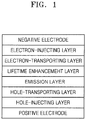
- Figure 1 is a schematic cross-sectional view of an organic light-emitting device according to an embodiment of the present invention.
- An organic light-emitting device includes a positive electrode, a negative electrode, and one or more organic material layers between the positive electrode and the negative electrode.
- the one or more of the organic material layers includes a HIL, a HTL, an EML, an ETL, and an EIL, and the EML includes a host material and a dopant material.
- a lifetime enhancement layer is positioned between the EML and the ETL.
- the lifetime enhancement layer includes a bipolar compound including an electron withdrawing group (EWG) capable of good (or substantial) electron absorption and an electron donating group (EDG) capable of good (or substantial) electron donation.
- EWG electron withdrawing group
- EDG electron donating group
- Most conventional electron or hole (carrier) transporting layer materials include a unipolar compound having either an EWG capable of substantial electron absorption or an EDG capable of good (or substantial) electron donation, thus selectively transporting either electrons or holes.
- the compound according to an embodiment of the present invention includes both the EWG and the EDG, and thus, exhibits bipolarity.
- the compound included in the lifetime enhancement layer according to an embodiment of the present invention has a hole-injecting energy barrier having an ionization potential of 5.5 eV or greater.
- a hole-injecting energy barrier having an ionization potential of 5.5 eV or greater.
- the compound included in the lifetime enhancement layer may have an ionization potential of 5.5 eV or greater, and in embodiments where the EML emits green or blue phosphorescent light, the compound included in the lifetime enhancement layer may have an ionization potential of 6.0 eV or greater.
- the lifetime enhancement layer has a triplet energy of 2.3 eV or greater to prevent diffusion of excitons generated in the EML into the ETL.
- the lifetime enhancement layer includes a compound that satisfies E HOMO -E LUMO > 3.0 eV and shows bipolarity, such that electron clouds of HOMO and LUMO are separated. Accordingly, the difference between triplet energy and singlet energy of the compound is small, so as to satisfy an equation of ⁇ E st ⁇ 0.5 eV (where ⁇ E st is the difference between the singlet energy (S1) and the triplet energy (T1) of the compound). Thus, high triplet energy (T1) may be shown even at an energy band gap of E HOMO -E LUMO > 3.0 eV.
- the compound included in the lifetime enhancement layer has a high triplet energy of 2.3 eV to prevent diffusion of excitons generated in the EML into the ETL of the organic light-emitting device. Accordingly, mixing of colors in an EL (electroluminescence) spectrum at the interface between the EML and the ETL may be prevented or reduced, and the stability and half-life of the organic light-emitting device may be increased.
- the compound included in the lifetime enhancement layer may have a triplet energy of 2.3 eV or greater, in embodiments where the EML emits green phosphorescent light, the compound included in the lifetime enhancement layer may have a triplet energy of 2.5 eV (or 2.5 eV or greater), and in embodiments where the EML emits blue phosphorescent light, the compound included in the lifetime enhancement layer may have a triplet energy of 2.7 eV (or 2.7 eV or greater).
- the lifetime enhancement layer includes an organic layer (e.g. an organic membrane layer) having a thickness of 1 ⁇ m or greater.
- organic layer e.g. an organic membrane layer
- hole mobility or electron mobility each measured through transit time of a carrier at room temperature
- the compound in the lifetime enhancement layer includes both the EWG and the EDG.
- hole mobility due to the EDG is 1 ⁇ 10 -6 cm 2 /V ⁇ s or greater at room temperature
- electron mobility due to the EWG is 1 ⁇ 10 -6 cm 2 /V ⁇ s or greater.
- hole mobility due to the EDG is from 1 ⁇ 10 -6 cm 2 /V ⁇ s to 1 ⁇ 10 -2 cm 2 /V ⁇ s at room temperature (e.g.
- the lifetime enhancement layer having a mobility of 1 ⁇ 10 -6 cm 2 /V ⁇ s prevents or reduces the delay in the injection of electrons from the negative electrode compared to the injection of holes from the positive electrode.
- the lifetime enhancement layer has a mobility of 1 ⁇ 10 -4 cm 2 /V ⁇ s. In other embodiments, the lifetime enhancement layer has a mobility of 1 ⁇ 10 -4 cm 2 /V ⁇ s or greater ( e.g. from 1 ⁇ 10 -4 cm 2 /V ⁇ s to 1 ⁇ 10 -2 cm 2 /V ⁇ s
- a bipolar compound in the lifetime enhancement layer the bipolar compound having a good electron-absorbing EWG and a good electron-donating EDG, is represented by Formula 1 below:
- the compound of Formula 1 may be represented by any one of Formulae A-1 to A-24 below, but the compound of Formula 1 is not limited thereto.
- R 2 , Y 1 to Y 4 , and Ar 1 to Ar 5 may be as described above in connection with Formula 1.
- Y 1 to Y 4 are each independently C(R 1 ), wherein R 1 may be described as above in connection with Formula 1.
- Y 1 and Y 4 are each independently C(R 1 ), wherein R 1 is H.
- Y 1 and Y 2 are each independently C(R 1 ), wherein R 1 is H.
- Y 3 and Y 4 are each independently C(R 1 ), wherein R 1 is H.
- Ar 1 is a C 6 -C 20 aryl group, preferably phenyl.
- R 2 is H.
- the compound of Formula 1 may be represented by Formulae A-1 to A-6, in order to facilitate the desired physical and chemical properties of the compound, but the compound of Formula 1 is not limited thereto.
- the compound represented by Formula 1 may be condensed with a compound represented by Formula 2 below.
- one of Y 1 and Y 2 , Y 2 and Y 3 , or Y 3 and Y 4 of Formula 1 may form a condensed ring with the compound represented by Formula 2.
- Y 1 to Y 4 of Formula 1 may be each independently, N or C(R 1 ), and a plurality of R 1 s may be the same or different.
- R 1 to R 3 and Ar 1 to Ar 5 may be each independently hydrogen, deuterium, a halogen group, a cyano group, a nitro group, an amino group, a C 1 -C 40 alkyl group, a C 2 -C 40 alkenyl group, a C 2 -C 40 alkynyl group, a C 3 -C 40 cycloalkyl group, a heterocycloalkyl group having 3 to 40 nuclear (i.e. ring) atoms, a C 6 -C 60 aryl group, a heteroaryl group having 5 to 60 (i.e.
- X 4 is N(Ar 1 ), wherein Ar 1 may be described as above in connection with Formula 2.
- Y 5 to Y 8 are each independently C(R 3 ), where a plurality of R 3 s may be the same or different and wherein R 3 may be described as above in connection with Formula 2, preferably wherein R 3 is selected from hydrogen or a C 1 -C 40 phosphine oxide group (e.g. a C 1 -C 30 , a C 10 -C 30 , a C 15 -C 30 , a C 15 -C 20 phosphine oxide group, such as a C 18 phosphine oxide group).
- Y 5 to Y 8 are each independently C(R 3 ), wherein R 3 is hydrogen.
- the resulting condensed compound may be represented by Formulae 1a to 1f:
- X 1 to X 4 and Y 1 to Y 8 may be as described above in connection with Formulae 1 and 2.
- Y 1 to Y 4 may be each independently N or C(R 1 ) and in some embodiments, may all be C(R 1 ) (preferably wherein R 1 is hydrogen); and Y 5 to Y 8 may each independently be N or C(R 3 ) and in some embodiments, may all be C(R 3 ) (preferably hydrogen or a C 1 -C 40 phosphine oxide group, more preferably hydrogen).
- a plurality of R 1 s and R 3 s may be each independently the same or different.
- X 1 is N(Ar 1 ), wherein Ar 1 may be as described above in connection with Formulae 1 and 2, preferably wherein Ar 1 is a C 6 -C 60 aryl group, preferably phenyl.
- X 1 is O.
- X 4 is N(Ar 1 ), wherein Ar 1 may be as described above in connection with Formulae 1 and 2.
- Y 5 to Y 8 are each independently C(R 3 ), where a plurality of R 3 s may be the same or different and wherein R 3 may be described as above in connection with Formula 2, preferably wherein R 3 is selected from hydrogen or a C 1 -C 40 phosphine oxide group (e.g. a C 1 -C 30 , a C 10 -C 30 , a C 15 -C 30 , a C 15 -C 20 phosphine oxide group, such as a C 18 phosphine oxide group).
- R 3 is preferably selected from H or a C 18 phosphine oxide group.
- the condensed compound may be represented by Formulae B-1 to B-30, but the condensed compound is not limited thereto.
- Ar 1 and R 1 to R 3 may be as described above in connection with Formulae 1 and 2.
- the condensed compound includes at least one of a condensed indole or a condensed carbazole moiety, in order to show strong EDG properties with good electron donation.
- R 1 to R 3 and Ar 1 to Ar 5 may be each independently selected from the group consisting of hydrogen, deuterium, a halogen group, a cyano group, a nitro group, an amino group, a C 1 -C 40 alkyl group, a C 2 -C 40 alkenyl group, a C 2 -C 40 alkynyl group, a C 3 -C 40 cycloalkyl group, a heterocycloalkyl group having 3 to 40 nuclear (i.e. ring) atoms, a C 6 -C 60 aryl group, a heteroaryl group having 5 to 60 (i.e.
- R 1 to R 3 may bind to a nearby group to form a condensed ring, and in some embodiments, R 1 to R 3 may include at least one moiety having strong electron-absorbing EWG, such as a heteroaryl group, a phosphine oxide group, or a cyano group.
- R 1 and R 3 are each independently represented by H.
- R 1 and R 3 are each independently selected from hydrogen or a C 1 -C 40 phosphine oxide group (e.g. a C 1 -C 30 , a C 10 -C 30 , a C 15 -C 30 , a C 15 -C 20 phosphine oxide group, such as a C 18 phosphine oxide group), wherein a plurality of R 1 s and R 3 s may be each independently the same or different.
- a C 1 -C 40 phosphine oxide group e.g. a C 1 -C 30 , a C 10 -C 30 , a C 15 -C 30 , a C 15 -C 20 phosphine oxide group, such as a C 18 phosphine oxide group
- R 2 is preferably hydrogen.
- R 2 is preferably phenyl.
- heteroaryl group may refer to a monovalent substituent derived from a monoheterocyclic or polyheterocyclic aromatic hydrocarbon having 5 to 40 nuclear (i.e. ring) atoms, where at least one carbon atom in the ring, and in some embodiments 1 to 3 carbons atoms in the ring, are substituted with a heteroatom such as N, O, S, or Se.
- the heteroaryl group contains two or more rings, the rings may be attached to each via a single bond or may be fused to each other, and may have a condensed form with an aryl group.
- Non-limiting examples of the heteroaryl include a 5-membered monocyclic ring such as furan, pyrrole, pyrroline, thiophene, pyrazole, pyrazoline, imidazole, oxazole, thiazole, oxadiazole, triazole, and thiadiazole; a 6-membered monocyclic ring such as pyridine, pyrazine, pyrimidine, pyridazine, and triazine; and a polycyclic ring such as benzofuran, benzothiophene, indole, benzimidazole, benzothiazole, purine, quinoline, isoquinoline, quinoxaline, naphthyridine, imidazopyridine, indazole, carbazole, phenoxazine, phenothiazine, and phenanthroline.
- the heteroaryl group may preferably be a 6-membered monocyclic ring (
- R 1 to R 3 and Ar 1 to Ar 5 may each independently be represented by Formulae C-1 to C-15.
- At least one of R 1 to R 3 and Ar 1 to Ar 5 includes a pyridine, a pyrazine, a pyrimidine, a pyridazine, a triazine, or a cyano group.
- an alkyl group may refer to a monovalent substituent derived from a linear or a branched chain of a C 1 -C 40 saturated hydrocarbon, and non-limiting examples of the alkyl group include a methyl group, an ethyl group, a propyl group, an isobutyl group, a sec-butyl group, a pentyl group, an iso-amyl group, a hexyl group, or the like.
- An alkenyl group may refer to a monovalent substituent derived from a linear or a branched chain of a C 2 -C 40 saturated hydrocarbon that includes at least one carbon-carbon double bond therein, and non-limiting examples of the alkenyl group include a vinyl group, an allyl group, an isopropenyl group, and a 2-butenyl group.
- An alkynyl group may refer to a monovalent substituent derived from a linear or a branched chain of a C 2 -C 40 saturated hydrocarbon that includes at least one carbon-carbon triple bond therein, and non-limiting examples of the alkynyl group include an ethynyl group and a 2-propynyl group.
- An aryl group may refer to a monovalent substituent derived from a C 6 -C 60 aromatic saturated hydrocarbon having at least one ring. When the aryl group includes two or more rings, the rings may be connected to each other via a single bond or may be fused to each other.
- Non-limiting examples of the aryl group include a phenyl group, a naphthyl group, a phenanthryl group, and an anthryl group.
- a heteroaryl group may refer to a monovalent substituent derived from a monoheterocyclic or a polyheterocyclic aromatic hydrocarbon having 5 to 40 nuclear (i.e. ring) atoms, in which at least one carbon atom in the ring, and in some embodiments 1 to 3 carbons atoms in the ring, are substituted with a heteroatom such as N, O, S, or Se.
- a heteroatom such as N, O, S, or Se.
- the heteroaryl group may be connected to each via a single bond or may be fused to each other.
- the heteroaryl group may also include a condensed shape with an aryl group.
- Non-limiting examples of the heteroaryl group include: a 6-membered monocyclic ring such as a pyridyl group, pyrazinyl group, a pyrimidinyl group, a pyridazinyl group, and a triazinyl group; a polycyclic ring such as a phenoxathienyl group, an indolizinyl group, an indolyl group, a purinyl group, a quinolyl group, a benzothiazole group, and a carbazolyl group; a 2-puranyl group; a N-imidazolyl group; a 2-isoxazolyl group;a 2-pyridinyl group; and a 2-pyrimidinyl group.
- a 6-membered monocyclic ring such as a pyridyl group, pyrazinyl group, a pyrimidinyl group, a pyridazinyl group, and
- An aryloxy group may refer to a monovalent substituent represented by RO-, where R is a C 5 -C 60 aryl group.
- R is a C 5 -C 60 aryl group.
- Non-limiting examples of the aryloxy group include a phenyloxy group, a naphthyloxy group, and a diphenyloxy group.
- An alkoxy group may refer to a monovalent substituent represented by R'O-, where R' is a linear, branched, or cyclic C 1 to C 40 alkyl group.
- R'O- a monovalent substituent represented by R'O-, where R' is a linear, branched, or cyclic C 1 to C 40 alkyl group.
- Non-limiting examples of the alkoxy group include a methoxy group, an ethoxy group, an n-propoxy group, a 1-propoxy group, a t-butoxy group, an n-butoxy group, and a pentoxy group.
- An arylamine group may refer to an amine group connected to a C 6 -C 60 aryl group.
- a cycloalkyl group may refer to a monovalent substituent derived from a C 3 -C 40 monocyclic or polycyclic non-aromatic hydrocarbon.
- Non-limiting examples of the cycloalkyl group include a cyclopropyl group, a cyclopentyl group, a cyclohexyl group, a norbornyl group, and an adamantane.
- a heterocycloalkyl group may refer to a monovalent substituent derived from a monocyclic or polycyclic hydrocarbon having 3 to 40 nuclear (i.e. ring) atoms, in which at least one carbon atom, and in some embodiments 1 to 3 carbon atoms, are substituted with a heteroatom such as N, O, S, or Se.
- Non-limiting examples of the heterocycloalkyl group include morpholine and piperazine.
- An alkylsilyl group may refer to a silyl group connected to a C 1 -C 40 alkyl group
- an arylsilyl group may refer to a silyl group connected to a C 5 -C 40 aryl group.
- a condensed ring may refer to a condensed aliphatic ring, a condensed aromatic ring, a condensed heteroaliphatic ring, a condensed heteroaromatic ring, or a combination thereof.
- An organic light-emitting device includes a positive electrode, a negative electrode, and at least one organic material layer between the positive electrode and the negative electrode, where the at least one organic material layer includes a hole-injecting layer (HIL), a hole-transporting layer (HTL), an emission layer (EML), an electron-transporting layer (ETL), and an electron-injecting layer (EIL).
- the EML includes a host material and a dopant material.
- a lifetime enhancement layer is positioned between the EML and the ETL.
- any suitable material may be used for the positive electrode in the organic light-emitting device according to an embodiment of the present invention
- the material for the positive electrode include a metal, such as vanadium (V), chromium (Cr), copper (Cu), zinc (Zn), and gold (Au), or an alloy thereof; a metal oxide such as zinc oxide, indium oxide, indium tin oxide (ITO), and indium zinc oxide (IZO); a combination of a metal and a metal oxide, such as ZnO:AI and SnO 2 :Sb; a conductive polymer such as polythiophene, poly(3-methyl thiophene), poly[3,4-(ethylene-1,2-dioxy)thiophene] (PEDT), polypyrrole, and polyaniline; and carbon black.
- a metal such as vanadium (V), chromium (Cr), copper (Cu), zinc (Zn), and gold (Au), or an alloy thereof
- a metal oxide such as zinc oxide, indium oxide
- any suitable material can be used for the negative electrode in the organic light-emitting device according to an embodiment of the present invention
- the material for the negative electrode include metals, such as magnesium (Mg), calcium (Ca), sodium (Na), potassium (K), titanium (Ti), indium (In), Yttrium (Y), lithium (Li), gadolinium (Gd), aluminum (Al), silver (Ag), tin (Sn), lead (Pb) or an alloy thereof; and a multi-layer structure material such as LiF/Al and LiO 2 /Al.
- the EIL and the ETL may respectively include an electron-injecting material and an electron-transporting material, each of which has high (or good) electron mobility and is capable of facilitating thorough electron injection.
- the compound capable of facilitating thorough electron injection includes a good electron-absorbing EWG and may be, for example, an anthracene derivative, a nitrogen-containing aromatic heterocyclic ring, or an alkali metal complex.
- the compound included in the ETL and the lifetime enhancement layer may be the same, and the compound included in the EIL and the lifetime enhancement layer may be the same.
- an alkali metal complex may be vacuum deposited on the EIL or the ETL.
- the metal complex may be an alkali metal, an alkaline earth metal, or a rare earth metal, but the metal complex is not limited thereto.
- the metal complex may be vacuum deposited on the EIL or the ETL to facilitate thorough injection of electrons from the negative electrode.
- the HTL and the HIL may respectively include a hole-transporting material and a hole-injecting material, each of which has high (or good) hole mobility and is capable of lowering a hole injection barrier.
- the hole-injecting material and the hole-transporting material each include an arylamine derivative.
- an organic membrane layer that is capable of blocking electrons and excitons may be positioned between the HTL and the EML.
- the organic membrane layer has a high lowest unoccupied molecular orbital (LUMO) value to block or suppress electrons from moving into the HTL, and a high triplet energy to prevent (or reduce) the diffusion of excitons from the EML into the HTL.
- the organic membrane layer capable of blocking or suppressing electrons from moving into the HTL may improve interface properties between the HTL and the EML, thus improving performance efficiency.
- the organic membrane layer includes a carbazole or an arylamine derivative.
- the EML includes the host material and the dopant material, each in an amount of about 0.1 wt% to about 30 wt% relative to the weight of the EML.
- the amount of the dopant may be from about 0.1 wt% to about 20 wt%, and when the EML emits blue, green, or red phosphorescent light, the amount of the dopant may be from about 1 wt% to about 30 wt%.
- the host compound i.e. host material
- the host compound can be any suitable compound including but not limited to an alkali metal complex, an alkaline earth metal complex, or a condensed aromatic ring derivative.
- the host compound may be an aluminum complex, a beryllium complex, an anthracene, or a pyrene derivative.
- the dopant compound i.e. dopant material
- the host compound can be any suitable compound having a structure in which various substituents are bound to a condensed aromatic ring or a condensed heteroaromatic ring.
- the host compound may include an anthracene derivative, a pyrene derivative, a triphenylene derivative, a carbazole derivative, a dibenzofuran derivative, and/or a dibenzothiopene derivative.
- the dopant compound include a metal complex or a metal complex including iridium (Ir) or platinum (Pt).
- the EML may include a single EML or a plurality of EMLs capable of achieving mixed color.
- the plurality of EMLs may be sequentially stacked between the HTL and the ETL to achieve mixed color when voltage and current are applied.
- the EMLs are stacked in series to achieve mixed color when voltage and current are applied, thus increasing efficiency in proportion to the number of the EMLs.
- a middle layer is positioned between the plurality of the EMLs and has the functions of both hole injection and electron injection, and the organic light-emitting device may exhibit an increase in the driving voltage in proportion to the number of EMLs. At the same time, though, the current in the device is maintained at a uniform level, thus improving the emission efficiency in proportion to the number of EMLs.
- the organic light-emitting device is capable of maintaining the maximum emission efficiency when voltage and current are applied, while substantially increasing the half-life of initial brightness.
- the organic light-emitting device includes a positive electrode, at least one organic material layer, and a negative electrode, which are sequentially stacked.
- the organic light-emitting device may include an insulation layer or an adhesive layer at the interface between the one of the positive and the negative electrode and the organic material layer.
- the organic light-emitting device may be manufactured via a method that should be apparent to one of ordinary skill in the art by using a different organic material layer and electrode than those described herein, as long as the lifetime enhancement layer of the present embodiments is positioned between the EML and the ETL of the organic material layer.
- the organic material layer may be formed by a vacuum deposition method or a solution coating method.
- the solution coating method include spin coating, dip coating, doctor blading, inkjet printing, or thermal transferring method, but the solution coating method is not limited thereto.
- Non-limiting examples of a substrate that may be included in the organic light-emitting device of the present embodiments include a silicon wafer, quartz, a glass plate, a metal plate, a plastic film, and a sheet.
- nitrobenzene was removed from the resulting mixture using methylene chloride to separate the organic layers, and then MgSO 4 was used to remove water from the organic layers, followed by further removing the solvent.
- 2,4-dibromoaniline (25.09 g, 0.1 mol) was added to a reactor and methylene chloride (100 ml) was further added thereto.
- Benzoyl chloride (11.6 mL, 0.1 mol) and pyridine (1.62 mL, 0.02 mol) were then slowly added to the reactor, mixed, and the resulting solution was stirred at room temperature for 2 hours to prepare a mixture.
- N-(2,4-dibromophenyl)benzamide (25.1 g, 71.0 mmol), K 2 CO 3 (19.6g, 142 mmol), and DMSO (710 ml) were mixed in a nitrogen current atmosphere, and the resulting solution was stirred at a temperature of 140°C for 1.5 hours to prepare a mixture.
- 6-bromo-2-phenylbenzo[d]oxazole (14.8 g, 54.0 mmol), 4,4,4',4',5,5, 5',5'-octamethyl-2,2'-bi(1,3,2-dioxaborolane) (15.1 g, 59.4 mmol), Pd(dppf)Cl 2 (6.24 g, 5.40 mmol), KOAc (15.25 g, 0.162 mol), and 1,4-dioxane (280 ml) were mixed in a nitrogen current atmosphere, and the resulting solution was stirred at a temperature of 130°C for 12 hours to prepare a mixture.
- 6-(2-nitrophenyl)-2-phenylbenzo[d]oxazole 11.05 g, 34.9 mmol
- triphenylphosphine 27.46 g, 104.7 mmol
- 1,2-dichlorobenzene 150 ml
- N -(2,4-dibromophenyl)benzamide (26.62 g, 0.075 mol) obtained from Process 1 in Preparation Example 3 was added to a reactor, toluene (300 ml) was added thereto, and the resulting mixture was stirred. Lawesson's reagent (22.92 g, 0.053 mol) was slowly added to the reactor in a drop-wise manner, mixed, and the resulting mixture was stirred at a temperature of 110 °C for 4 hours to obtain a product.
- N -(2,4-dibromophenyl)benzothioamide (26.35 g, 71.0 mmol) obtained from Process 1 in Preparation Example 4 was mixed in a nitrogen current atmosphere with K 2 CO 3 (19.63 g, 142 mmol), and DMSO (710 ml), and the resulting solution was stirred at a temperature of 140 °C for 1.5 hours to prepare a mixture.
- IC-1 (3 g, 10.63 mmol), 2-(3-chlorophenyl)-4,6-diphenyl-1,3,5-triazine (4.38 g, 12.75 mmol), Pd(OAc) 2 (0.12 g, 5 mol%), NaO(t-bu) (2.04 g, 21.25 mmol), P(t-bu) 3 (0.21 g, 1.06 mmol), and toluene (100 ml) were mixed in a nitrogen current atmosphere, and the resulting solution was stirred at a temperature of 110°C for 12 hours to prepare a mixture.
- Embodiments of the present invention are not limited to the compounds described herein, and may be synthesized by one of ordinary skill in the art using similar synthesis methods to those described herein.
- a glass substrate coated with ITO (Indium tin oxide) having a thickness of 1500 ⁇ was ultrasonically washed with distilled water, followed by washing with a solvent, such as isopropyl alcohol, acetone, and/or methanol.
- the substrate was then dried and transported to a UV OZONE washer (Power sonic 405, available from Hwashin Tech) to be washed with UV for 5 minutes, and then was transported to a vacuum deposition apparatus.
- an organic light-emitting device was manufactured on the ITO transparent substrate prepared as described above.
- a lifetime enhancement layer of each of the manufactured organic light-emitting devices included one of compounds LE-01 to LE-28.
- the layers included in the organic light-emitting device are listed in the top row of Table 2.
- Table 2 HIL HTL EML Lifetime Enhancement layer
- ETL EIL Negative electrode Compound DS-205 (available from Doosan) NPB ADN and 5 % DS-405 (available from Doosan) LE-01 - LE-28 Alq3 LiF Al Thickness 80 nm 15 nm 30 nm 5nm 25 nm 1 nm 200 nm
- NPB, ADN and Alq 3 are as follows:
- An organic light-emitting device was manufactured as in Example 1, except that a lifetime enhancement layer was not used and the ETL had a thickness of 30nm.
- An organic light-emitting device was manufactured as in Example 1, except that BCP was used instead of LE-01 in a lifetime enhancement layer.
- a glass substrate coated with ITO (Indium tin oxide) having a thickness of 1500 ⁇ was ultrasonically washed with distilled water, followed by ultrasonic washing with a solvent, such as isopropyl alcohol, acetone, and/or methanol.
- the resulting substrate was dried and transported to a UV OZONE washer (Power sonic 405, available from Hwashin Tech) to be washed with UV for 5 minutes, and then was transported to a vacuum deposition apparatus.
- a solvent such as isopropyl alcohol, acetone, and/or methanol
- a green phosphorescent organic light-emitting device was manufactured on the ITO transparent substrate prepared as described above.
- a lifetime enhancement layer of each of the manufactured organic light-emitting devices included one of LE-04, LE-08, LE-11, LE-12, LE-15, LE-16, LE-17, and LE-18.
- the layers included in the organic light-emitting device are listed in the top row of Table 3.
- An organic light-emitting device was manufactured as in Example 1, except that a lifetime enhancement layer was not used and the ETL had a thickness of 30 nm.
- An organic light-emitting device was manufactured as in Example 29, except that BCP was used instead of LE-04 in a lifetime enhancement layer.
- the organic light-emitting devices of Examples 1 to 28 and Examples 29 to 36 which included the lifetime enhancement layer according to embodiments of the present invention, showed good current efficiency, low driving voltage, and good half-life, as compared to the organic light-emitting devices of Comparative Examples 1 to 4, which did not include the lifetime enhancement layer according to embodiments of the present invention.
- Some of the organic light-emitting devices of Examples 1 to 28 and Examples 29 to 36 also showed long lifetime (T 97 ).
- the organic light-emitting devices according to embodiments of the present invention have low driving voltage, high efficiency, and a long lifetime.
Landscapes
- Physics & Mathematics (AREA)
- Chemical & Material Sciences (AREA)
- Engineering & Computer Science (AREA)
- Materials Engineering (AREA)
- Spectroscopy & Molecular Physics (AREA)
- Optics & Photonics (AREA)
- Organic Chemistry (AREA)
- Electroluminescent Light Sources (AREA)
Claims (13)
- Organische lichtemittierende Vorrichtung, umfassend:eine positive Elektrode;eine negative Elektrode; undmindestens eine organische Materialschicht zwischen der positiven Elektrode und der negativen Elektrode, wobeidie mindestens eine organische Materialschicht eine Lochinjektionsschicht, eine Lochtransportschicht, eine Emissionsschicht umfasst, umfassend ein Wirtsmaterial und ein Dotierstoffmaterial, eine Elektronentransportschicht, eine Elektroninjektionsschicht undeine Schicht zur Erhöhung der Lebensdauer zwischen der Emissionsschicht und der Elektronentransportschicht, wobei die Schicht zur Erhöhung der Lebensdauer eine bipolare Verbindung umfasst, die eine elektronenziehende Gruppe (EWG) und eine elektronenspendende Gruppe (EDG) umfasst, wobei die bipolare Verbindung ein gemessenes Ionisationspotential von 5,5 eV oder größer, eine gemessene Differenz zwischen einer Energie des am höchsten besetzten Molekülorbitals und einer Energie des am niedrigsten besetzten Molekülorbitals von mehr als 3,0 eV aufweist, eine gemessene Triplett-Energie von 2,3 eV oder mehr und eine unter Verwendung von B3LYP/6-31G* berechnete Differenz zwischen einer Singulett-Energie und der Triplett-Energie von weniger als 0,5 eV, wobei die Singulett-Energie (S1) ist Triplett-Energie (T1) ist; undwobei die bipolare Verbindung eine Verbindung ist, die dargestellt wird durch Formel 1:
 X1 ausgewählt ist aus der Gruppe bestehend aus O, S, Se, N(Ar1), C(Ar1), C(Ar2)(Ar3) und Si(Ar4)(Ar5),Y1 bis Y4 jeweils unabhängig N oder C(R1) sind, wobei eine Vielzahl von R1 gleich oder verschieden sind und ein oder mehrere R1 wahlweise an einer nahe befindlichen Gruppe binden, um einen kondensierten Ring zu bilden; undX2 und X3 jeweils unabhängig N oder C(R2) sind, wobei eine Vielzahl von R2 gleich oder verschieden ist und ein oder mehrere R2 wahlweise an einer nahe befindlichen Gruppe binden, um einen kondensierten Ring zu bilden;R1 bis R2 und Ar1 bis Ar2 jeweils unabhängig ausgewählt sind aus der Gruppe bestehend aus einem Wasserstoff, einem Deuterium, einer Halogen-Gruppe, einer Cyano-Gruppe, einer Nitro-Gruppe, einer Amino-Gruppe, einer C1- bis C40-Alkyl-Gruppe, einer C2- bis C40-Alkenyl-Gruppe, einer C2- bis C40-Alkinyl-Gruppe, einer C3- bis C40-Cycloalkyl-Gruppe, einer Heterocycloalkyl-Gruppe, die 3 bis 40 Ringatome aufweist, einer C6- bis C60-Aryl-Gruppe, einer C1- bis C40-Alkoxy-Gruppe, einer C6-C60-Aryloxy-Gruppe, einer C1- bis C40-Alkylsilyl-Gruppe, einer C6-C60-Arylsilyl-Gruppe, einer C1- bis C40-Alkylbor-Gruppe, einer C6- bis C60-Arylbor-Gruppe, einer C1-C40-Phosphin-Gruppe, einer C1-C40-Phosphinoxid-Gruppe und einer C6-C60-Arylamin-Gruppe, undeiner C1- bis C40-Alkyl-Gruppe, einer C2- bis C40-Alkenyl-Gruppe, einer C2- bis C40-Alkinyl-Gruppe, einer C3- bis C40-Cycloalkyl-Gruppe, einer Heterocycloalkyl-Gruppe, die 3 bis 40 Ringatome aufweist, einer C6- bis C60-Aryl-Gruppe, einer C1- bis C40-AlkoxyGruppe, einer C6-C60-Aryloxy-Gruppe, einer C1- bis C40-Alkylsilyl-Gruppe, einer C6-C60-Arylsilyl-Gruppe, einer C1- bis C40-Alkylbor-Gruppe, einer C6- bis C60-Arylbor-Gruppe, einer C1-C40-Phosphin-Gruppe, einer C1-C40-Phosphinoxid-Gruppe und einer C6-C60-Arylamin-Gruppe, die jeweils unabhängig substituiert sind mit einer der folgenden, die ausgewählt ist aus der Gruppe bestehend aus einem Deuterium, einer Halogen-Gruppe, einer Cyano-Gruppe, einer Nitro-Gruppe, einer Amino-Gruppe, einer C1- bis C40-AlkylGruppe, einer C2- bis C40-Alkenyl-Gruppe, einer C2- bis C40-Alkinyl-Gruppe, einer C3- bis C40-Cycloalkyl-Gruppe, einer Heterocycloalkyl-Gruppe, die 3 bis 40 Ringatome aufweist, einer C6- bis C40-Aryl-Gruppe, einer C1- bis C40-Alkoxy-Gruppe, einer C6-C60-AryloxyGruppe, einer C1- bis C40-Alkylsilyl-Gruppe, einer C6-C60-Arylsilyl-Gruppe, einer C1- bis C40-Alkylbor-Gruppe, einer C6- bis C60-Arylbor-Gruppe, einer C1-C40-Phosphin-Gruppe, einer C1-C40-Phosphinoxid-Gruppe und einer C6-C60-Arylamin-Gruppe; undeiner Gruppe, die dargestellt wird durch Formeln C-1 bis C-15:wobei in den Formeln C-1 bis C-15:


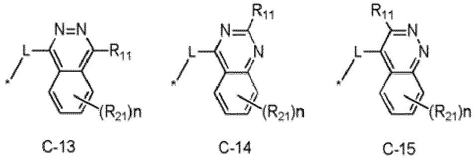 L eine Einfachbindung ist, die ausgewählt ist aus der Gruppe bestehend aus einer C6- bis C18-Arylen-Gruppe und einer Heteroarylen-Gruppe, die 5 bis 18 Ringatome aufweist;R11 und R21 gleich oder verschieden sind und jeweils unabhängig ausgewählt sind aus der Gruppe bestehend aus Wasserstoff, Deuterium, einer Halogen-Gruppe, einer Cyano-Gruppe, einer Nitro-Gruppe, einer Amino-Gruppe, einer C1-bis C40-Alkyl-Gruppe, einer C2- bis C40-Alkenyl-Gruppe, einer C2- bis C40-Alkinyl-Gruppe, einer C3- bis C40-Cycloalkyl-Gruppe, einer Heterocycloalkyl-Gruppe, die 3 bis 40 Ringatome aufweist, einer C6- bis C60-Aryloxy-Gruppe, einer Heteroaryl-Gruppe, die 5 bis 60 Ringatome aufweist, einer C1- bis C40-Alkoxy-Gruppe, einer C6- bis C60-Aryloxy-Gruppe, einer C1- bis C40-Alkylsilyl-Gruppe, einer C6- bis C60-Arylsilyl-Gruppe, einer C1- bis C40-Alkylbor-Gruppe, einer C6- bis C60-Arylbor-Gruppe, einer C1- bis C60-Phosphine-Gruppe, einer C1- bis C60-Phosphinoxid-Gruppe und einer C6- bis C60-Arylamin-Gruppe, und R11 und R12 durch Binden an einer nahe befindlichen Gruppe jeweils einen kondensierten Ring bilden können; undn eine ganze Zahl von 0 bis 4 ist.
 - Organische lichtemittierende Vorrichtung nach Anspruch 1, wobei, wenn die Emissionsschicht blaues fluoreszierendes Licht, grünes fluoreszierendes Licht oder rotes phosphoreszierendes Licht emittiert, die in der Schicht zur Erhöhung der Lebensdauer enthaltene Verbindung eine gemessene Triplett-Energie von 2,3 eV oder mehr aufweist.
- Organische Licht emittierende Vorrichtung nach Anspruch 1, wobei, wenn die Emissionsschicht grünes phosphoreszierendes Licht emittiert, die bipolare Verbindung eine gemessene Triplett-Energie von 2,5 eV oder mehr und ein gemessenes Ionisationspotential von 6,0 eV oder mehr aufweist.
- Organische Licht emittierende Vorrichtung nach Anspruch 1, wobei, wenn die Emissionsschicht blaues phosphoreszierendes Licht emittiert, die bipolare Verbindung eine gemessene Triplett-Energie von 2,7 eV oder mehr und ein gemessenes Ionisationspotential von 6,0 eV oder mehr aufweist.
- Organische Licht emittierende Vorrichtung nach einem der Ansprüche 1 bis 4, wobei
die Schicht zur Verbesserung der Lebensdauer eine organische Membranschicht mit einer Dicke von 1 µm oder mehr umfasst, und
Elektronenbeweglichkeit und Löcherbeweglichkeit, gemessen durch Laufzeit eines Trägers bei Raumtemperatur, jeweils mindestens 1 × 10⁻⁶ cm2/V.s betragen. - Organische Licht emittierende Vorrichtung nach einem der Ansprüche 1 bis 5, wobei die durch Formel 1 dargestellte Verbindung dargestellt wird durch Formeln A-1 bis A-24:


- Organische Licht emittierende Vorrichtung nach einem der Ansprüche 1 bis 6, wobei jeder Y1 und Y2, Y2 und Y3 oder Y3 und Y4 der durch Formel 1 dargestellten Verbindung einen kondensierten Ring mit einer Verbindung bildet, die durch Formel 2 dargestellt wird:
 eine gestrichelte Linie einen Abschnitt darstellt, wo die durch Formel 2 dargestellte Verbindung mit der durch Formel 1 dargestellten Verbindung kondensiert ist,Y5 bis Y8 jeweils unabhängig N oder C(R3) sind, wobei eine Vielzahl von R3 gleich oder verschieden sind,X4 ausgewählt ist aus der Gruppe bestehend aus O, S, Se, N(Ar1), C(Ar2)(Ar3) und Si(Ar4)(Ar5),mindestens eines von X1 und X4 N(Ar1) ist,R1 bis R3 und Ar1 bis Ars jeweils unabhängig ausgewählt sind aus der Gruppe bestehend aus Wasserstoff, Deuterium, einer Halogen-Gruppe, einer Cyano-Gruppe, einer Nitro-Gruppe, einer Amino-Gruppe, einer C1- bis C40-Alkyl-Gruppe, einer C2- bis C40-Alkenyl-Gruppe, einer C2- bis C40-Alkinyl-Gruppe, einer C3- bis C40-Cycloalkyl-Gruppe einer Heterocycloalkyl-Gruppe, die 3 bis 40 Ringatome aufweist, einer C6- bis C60-ArylGruppe, einer Heteroaryl-Gruppe, die 5 bis 60 Ringatome aufweist, einer C1- bis C40-Alkoxy-Gruppe, einer C6-C60-Aryloxy-Gruppe, einer C1- bis C40-Alkylsilyl-Gruppe, einer C6-C60-Arylsilyl-Gruppe, einer C1- bis C40-Alkylbor-Gruppe, einer C6- bis C60-Arylbor-Gruppe, einer C1- bis C40-Phosphin-Gruppe, einer C1- bis C40-Phosphinoxid-Gruppe und einer C6- bis C60-Arylamin-Gruppe, undeiner C1- bis C40-Alkyl-Gruppe, einer C2- bis C40-Alkenyl-Gruppe, einer C2- bis C40-Alkinyl-Gruppe, einer C3- bis C40-Cycloalkyl-Gruppe, einer Heterocycloalkyl-Gruppe, die 3 bis 40 Ringatome aufweist, einer C6- bis C60-Aryl-Gruppe, einer Heteroaryl-Gruppe, die 5 bis 60 Ringatome aufweist, einer C1- bis C40-Alkoxy-Gruppe, einer C6- bis C60-Aryloxy-Gruppe, einer C1- bis C40-Alkylsilyl-Gruppe, einer C6- bis C60-Arylsilyl-Gruppe, einer C1- bis C40-Alkylbor-Gruppe, einer C6- bis C60-Arylbor-Gruppe, einer C1- bis C40-Phosphin-Gruppe, einer C1- bis C40-Phosphinoxid-Gruppe und einer C6- bis C60-Arylamin-Gruppe, die jeweils unabhängig substituiert sind mit einer der folgenden, die ausgewählt ist aus der Gruppe bestehend aus einem Deuterium, einer Halogen-Gruppe, einer Cyano-Gruppe, einer Nitro-Gruppe, einer Amino-Gruppe, einer C1- bis C40-Alkyl-Gruppe, einer C2- bis C40-Alkenyl-Gruppe, einer C2- bis C40-Alkinyl-Gruppe, einer C3- bis C40-Cycloalkyl-Gruppe, einer Heterocycloalkyl-Gruppe, die 3 bis 40 Ringatome aufweist, einer C6- bis C40-Aryl-Gruppe, einer Heteroaryl-Gruppe, die 5 bis 40 Ringatome aufweist, einer C1- bis C40-Alkoxy-Gruppe, einer C6- bis C60-Aryloxy-Gruppe, einer C1- bis C40-Alkylsilyl-Gruppe, einer C6- bis C60-Arylsilyl-Gruppe, einer C1- bis C40-Alkylbor-Gruppe, einer C6- bis C60-Arylbor-Gruppe, einer C1- bis C40-Phosphin-Gruppe, einer C1- bis C40-Phosphinoxid-Gruppe und einer C6- bis C60-Arylamin-Gruppe; undR1 bis R3 wahlweise an einer nahe befindlichen Gruppe binden, um einen kondensierten Ring zu bilden.
 - Organische Licht emittierende Vorrichtung nach Anspruch 7, wobei die Verbindung, die gebildet wird, wenn die durch Formel 1 dargestellte Verbindung mit der durch Formel 2 dargestellten Verbindung kondensiert ist, ein Verbindung ist, die durch eine beliebige Verbindung dargestellt wird, die ausgewählt ist aus Formeln 1a bis 1f:


- Organische Licht emittierende Vorrichtung nach Anspruch 7 oder Anspruch 8, wobei die Verbindung, die gebildet wird, wenn die durch Formel 1 dargestellte Verbindung mit der durch Formel 2 dargestellten Verbindung kondensiert ist, eine Verbindung ist, die durch eine beliebige der Verbindungen dargestellt wird, die ausgewählt sind aus Formeln B-1 bis B-30:


- Organische Licht emittierende Vorrichtung nach einem der Ansprüche 1 bis 9, worin mindestens eines von R1 bis R3 und Ar1 bis Ar5 eine Cyano-Gruppe, eine Heterocycloalkyl-Gruppe, die 3 bis 40 Ringatome aufweist, und/oder eine C1- bis C60-Phosphinoxid-Gruppe umfasst, vorzugsweise
wobei mindestens eine von R1 bis R3 und Ar1 bis Ar5 eine Pyridin-, eine Pyrazin-, eine Pyrimidin-, eine Pyridazin-, eine Triazin- und/oder eine Cyano-Gruppe umfasst. - Organische Licht emittierende Vorrichtung nach einem der vorhergehenden Ansprüche, wobei die Elektronentransportschicht und die Schicht zur Erhöhung der Lebensdauer dieselbe Verbindung umfassen; und/oder
wobei die Elektroninjektionsschicht und die Schicht zur Erhöhung der Lebensdauer dieselbe Verbindung umfassen; und/oder
wobei sich ein Alkalimetall-Komplex auf der Elektroninjektionsschicht oder der Elektronentransportschicht befindet; und/oder
wobei sich eine organische Membranschicht, die ausgelegt ist, um Elektronen und Exzitonen zu blockieren, zwischen der Löchertransportschicht und der Emissionsschicht befindet. - Organische Licht emittierende Vorrichtung nach einem der vorhergehenden Ansprüche, wobei die Emissionsschicht einen Dotierstoff in einer Menge von etwa 0,1% bis etwa 30 Gew.-% umfasst.
- Organische Licht emittierende Vorrichtung nach einem der vorhergehenden Ansprüche, wobei eine Vielzahl der Emissionsschichten zwischen der Löchertransportschicht und der Elektronentransportschicht ausgelegt ist, um eine Mischfarbe zu zeigen, wenn Spannung und Strom an ihnen angelegt sind; und/oder
wobei eine Vielzahl der Emissionsschichten aus dem gleichen Material oder verschiedenen Materialien ausgebildet und zwischen der Löchertransportschicht und der Elektronentransportschicht gestapelt sind, um eine Mischfarbe zu zeigen und/oder die Leistungsfähigkeitzu erhöhen, wenn Spannung und Strom an ihnen angelegt sind.
Applications Claiming Priority (1)
| Application Number | Priority Date | Filing Date | Title |
|---|---|---|---|
| KR1020140006264A KR102221106B1 (ko) | 2014-01-17 | 2014-01-17 | 유기 발광 소자 |
Publications (2)
| Publication Number | Publication Date |
|---|---|
| EP2897185A1 EP2897185A1 (de) | 2015-07-22 |
| EP2897185B1 true EP2897185B1 (de) | 2020-12-16 |
Family
ID=52347225
Family Applications (1)
| Application Number | Title | Priority Date | Filing Date |
|---|---|---|---|
| EP15151515.2A Active EP2897185B1 (de) | 2014-01-17 | 2015-01-16 | Organische lichtemittierende Vorrichtung |
Country Status (4)
| Country | Link |
|---|---|
| US (1) | US9543538B2 (de) |
| EP (1) | EP2897185B1 (de) |
| KR (1) | KR102221106B1 (de) |
| CN (1) | CN104795504B (de) |
Families Citing this family (26)
| Publication number | Priority date | Publication date | Assignee | Title |
|---|---|---|---|---|
| KR101742359B1 (ko) | 2013-12-27 | 2017-05-31 | 주식회사 두산 | 유기 전계 발광 소자 |
| US9478763B2 (en) * | 2014-04-04 | 2016-10-25 | Seiko Epson Corporation | Light emitting element, light emitting device, display apparatus, and electronic equipment having a light emitting layer with host and assist dopant materials with different electron and hole transportation properties |
| KR102369595B1 (ko) * | 2014-12-08 | 2022-03-04 | 삼성디스플레이 주식회사 | 유기 발광 소자 및 이를 포함하는 표시 장치 |
| EP3051604B1 (de) | 2015-01-30 | 2017-10-11 | Samsung Display Co., Ltd. | Organische lichtemittierende vorrichtung |
| KR20170016701A (ko) * | 2015-08-04 | 2017-02-14 | 주식회사 두산 | 유기 발광 화합물 및 이를 이용한 유기 전계 발광 소자 |
| KR20170034067A (ko) * | 2015-09-18 | 2017-03-28 | 엘지디스플레이 주식회사 | 유기 발광 표시 장치 |
| KR102627398B1 (ko) | 2015-12-11 | 2024-01-22 | 삼성디스플레이 주식회사 | 축합환 화합물 및 이를 포함한 유기 발광 소자 |
| EP3182478B1 (de) | 2015-12-18 | 2018-11-28 | Novaled GmbH | Elektroneninjektionsschicht für eine organische leuchtdiode (oled) |
| KR20170075122A (ko) * | 2015-12-22 | 2017-07-03 | 삼성디스플레이 주식회사 | 유기 발광 소자 |
| KR102579752B1 (ko) | 2015-12-22 | 2023-09-19 | 삼성디스플레이 주식회사 | 유기 발광 소자 |
| KR102384293B1 (ko) | 2015-12-22 | 2022-04-08 | 삼성디스플레이 주식회사 | 유기 발광 소자 |
| KR20170075114A (ko) | 2015-12-22 | 2017-07-03 | 삼성디스플레이 주식회사 | 유기 발광 소자 |
| EP3208861A1 (de) | 2016-02-19 | 2017-08-23 | Novaled GmbH | Elektronentransportschicht mit einer matrixverbindungsmischung für eine organische leuchtdiode (oled) |
| KR102642199B1 (ko) | 2016-04-07 | 2024-03-05 | 삼성디스플레이 주식회사 | 유기 발광 소자 |
| KR101958059B1 (ko) * | 2016-07-29 | 2019-03-14 | 엘지디스플레이 주식회사 | 유기 발광 표시 장치 |
| JP6717150B2 (ja) * | 2016-10-05 | 2020-07-01 | コニカミノルタ株式会社 | 有機エレクトロニクス素子、及び、電子機器 |
| KR102746486B1 (ko) * | 2016-12-23 | 2024-12-26 | 솔루스첨단소재 주식회사 | 유기 화합물 및 이를 포함하는 유기 전계 발광 소자 |
| DE102017111137B4 (de) | 2017-05-22 | 2025-07-10 | Novaled Gmbh | Organische elektrolumineszente Vorrichtung |
| KR101884130B1 (ko) * | 2017-08-29 | 2018-07-31 | 주식회사 두산 | 유기 전계 발광 소자 |
| KR102654919B1 (ko) | 2018-07-23 | 2024-04-05 | 삼성디스플레이 주식회사 | 유기 발광 소자 |
| CN108963098B (zh) * | 2018-08-03 | 2020-04-28 | 京东方科技集团股份有限公司 | 一种qled显示面板及其制备方法、显示装置 |
| WO2020050563A1 (ko) * | 2018-09-03 | 2020-03-12 | 주식회사 엘지화학 | 유기 발광 소자 |
| CN109096281A (zh) * | 2018-09-05 | 2018-12-28 | 武汉市晟承宇科技有限公司 | 一种用于有机电致发光器件的化合物 |
| CN110783473B (zh) * | 2019-10-31 | 2022-10-21 | 昆山国显光电有限公司 | 一种发光器件和显示面板 |
| JP7668101B2 (ja) * | 2020-11-06 | 2025-04-24 | JDI Design and Development 合同会社 | 有機el素子、有機elパネル、および、有機el素子の製造方法 |
| CN118019372A (zh) * | 2024-01-16 | 2024-05-10 | 武汉华星光电半导体显示技术有限公司 | 一种显示面板及显示装置 |
Family Cites Families (8)
| Publication number | Priority date | Publication date | Assignee | Title |
|---|---|---|---|---|
| KR100560789B1 (ko) * | 2003-11-25 | 2006-03-13 | 삼성에스디아이 주식회사 | 풀칼라유기전계발광소자 및 그의 제조방법 |
| JP4947909B2 (ja) | 2004-03-25 | 2012-06-06 | 三洋電機株式会社 | 有機エレクトロルミネッセンス素子 |
| US9051344B2 (en) * | 2005-05-06 | 2015-06-09 | Universal Display Corporation | Stability OLED materials and devices |
| EP2133932A4 (de) | 2007-03-23 | 2011-06-22 | Idemitsu Kosan Co | Organische el-einrichtung |
| US8034465B2 (en) * | 2007-06-20 | 2011-10-11 | Global Oled Technology Llc | Phosphorescent oled having double exciton-blocking layers |
| KR100924144B1 (ko) | 2008-06-05 | 2009-10-28 | 삼성모바일디스플레이주식회사 | 유기전계발광소자 및 그의 제조 방법 |
| CN102668160B (zh) * | 2010-11-22 | 2016-06-22 | 出光兴产株式会社 | 有机电致发光器件 |
| US20120126205A1 (en) | 2010-11-22 | 2012-05-24 | Idemitsu Kosan Co., Ltd. | Organic electroluminescence device |
-
2014
- 2014-01-17 KR KR1020140006264A patent/KR102221106B1/ko active Active
- 2014-10-31 US US14/530,637 patent/US9543538B2/en active Active
-
2015
- 2015-01-14 CN CN201510017737.9A patent/CN104795504B/zh active Active
- 2015-01-16 EP EP15151515.2A patent/EP2897185B1/de active Active
Non-Patent Citations (1)
| Title |
|---|
| None * |
Also Published As
| Publication number | Publication date |
|---|---|
| CN104795504B (zh) | 2018-12-07 |
| US20150207093A1 (en) | 2015-07-23 |
| KR20150086095A (ko) | 2015-07-27 |
| US9543538B2 (en) | 2017-01-10 |
| EP2897185A1 (de) | 2015-07-22 |
| KR102221106B1 (ko) | 2021-03-02 |
| CN104795504A (zh) | 2015-07-22 |
Similar Documents
| Publication | Publication Date | Title |
|---|---|---|
| EP2897185A1 (de) | Organische lichtemittierende Vorrichtung | |
| EP3305792B1 (de) | Stickstoffhaltige kondensierte zyklische verbindung und organisches lichtemittierendes element damit | |
| EP3854792A1 (de) | Neuartige verbindung und organische lichtemittierende diode damit | |
| EP3428163B1 (de) | Polycyclische verbindung und organisches lichtemittierendes element damit | |
| EP3137451B1 (de) | Elektronentransportmaterial und organische elektrolumineszenzvorrichtung damit | |
| EP3862350B1 (de) | Neuartige verbindung und organische lichtemittierende vorrichtung mit verwendung davon | |
| EP3835299B1 (de) | Neuartige heterocyclische verbindung und organische lichtemittierende vorrichtung mit verwendung davon | |
| CN112397664B (zh) | 杂环化合物和包含其的有机发光器件 | |
| CN113039183B (zh) | 新型化合物及包含其的有机发光器件 | |
| EP3415585B1 (de) | Organisches lichtemittierendes element | |
| KR102392663B1 (ko) | 신규한 화합물 및 이를 이용한 유기 발광 소자 | |
| EP3483152B1 (de) | Verbindung und organische lichtemittierende vorrichtung damit | |
| CN114503297A (zh) | 第一和第二有机半导体层以及包括所述第一和第二有机半导体层的有机电子器件 | |
| KR102729197B1 (ko) | 유기 화합물 및 이를 이용한 유기 전계 발광 소자 | |
| KR102126884B1 (ko) | 헤테로 고리 화합물 및 이를 이용한 유기발광 소자 | |
| CN113423706A (zh) | 新型化合物及包含其的有机发光器件 | |
| KR20200035905A (ko) | 신규한 화합물 및 이를 이용한 유기발광 소자 | |
| EP3263555A1 (de) | Heteroringverbindung und organisches lumineszierendes element damit | |
| CN113454078A (zh) | 新型杂环化合物及包含其的有机发光器件 | |
| KR20190118821A (ko) | 축합환 화합물 및 이를 포함한 유기 발광 소자 | |
| KR102103506B1 (ko) | 신규한 헤테로 고리 화합물 및 이를 이용한 유기발광 소자 | |
| EP3029034A1 (de) | Benzotriazolderivat und organisches elektrolumineszentes element | |
| KR102924600B1 (ko) | 유기 화합물 및 이를 이용한 유기 전계 발광 소자 | |
| CN112703192B (zh) | 化合物及包含其的有机发光器件 | |
| KR102703928B1 (ko) | 유기 화합물 및 이를 포함하는 유기 전계 발광 소자 |
Legal Events
| Date | Code | Title | Description |
|---|---|---|---|
| PUAI | Public reference made under article 153(3) epc to a published international application that has entered the european phase |
Free format text: ORIGINAL CODE: 0009012 |
|
| 17P | Request for examination filed |
Effective date: 20150116 |
|
| AK | Designated contracting states |
Kind code of ref document: A1 Designated state(s): AL AT BE BG CH CY CZ DE DK EE ES FI FR GB GR HR HU IE IS IT LI LT LU LV MC MK MT NL NO PL PT RO RS SE SI SK SM TR |
|
| AX | Request for extension of the european patent |
Extension state: BA ME |
|
| RAP1 | Party data changed (applicant data changed or rights of an application transferred) |
Owner name: DOOSAN CORPORATION Owner name: SAMSUNG DISPLAY CO., LTD. |
|
| RIN1 | Information on inventor provided before grant (corrected) |
Inventor name: BEAK, YOUNGMI Inventor name: LEE, CHANG JUN Inventor name: KIM, MIKYUNG Inventor name: EUM, MIN-SIK Inventor name: PARK, HOCHEOL Inventor name: KIM, TAE HYUNG Inventor name: SHIN, DONGWOO Inventor name: LEE, EUNJUNG Inventor name: KIM, SEULONG Inventor name: CHU, CHANGWOONG |
|
| 17P | Request for examination filed |
Effective date: 20160115 |
|
| RBV | Designated contracting states (corrected) |
Designated state(s): AL AT BE BG CH CY CZ DE DK EE ES FI FR GB GR HR HU IE IS IT LI LT LU LV MC MK MT NL NO PL PT RO RS SE SI SK SM TR |
|
| STAA | Information on the status of an ep patent application or granted ep patent |
Free format text: STATUS: EXAMINATION IS IN PROGRESS |
|
| 17Q | First examination report despatched |
Effective date: 20191010 |
|
| RAP1 | Party data changed (applicant data changed or rights of an application transferred) |
Owner name: DOOSAN SOLUS CO., LTD. Owner name: SAMSUNG DISPLAY CO., LTD. |
|
| GRAP | Despatch of communication of intention to grant a patent |
Free format text: ORIGINAL CODE: EPIDOSNIGR1 |
|
| STAA | Information on the status of an ep patent application or granted ep patent |
Free format text: STATUS: GRANT OF PATENT IS INTENDED |
|
| INTG | Intention to grant announced |
Effective date: 20200703 |
|
| GRAS | Grant fee paid |
Free format text: ORIGINAL CODE: EPIDOSNIGR3 |
|
| GRAA | (expected) grant |
Free format text: ORIGINAL CODE: 0009210 |
|
| STAA | Information on the status of an ep patent application or granted ep patent |
Free format text: STATUS: THE PATENT HAS BEEN GRANTED |
|
| AK | Designated contracting states |
Kind code of ref document: B1 Designated state(s): AL AT BE BG CH CY CZ DE DK EE ES FI FR GB GR HR HU IE IS IT LI LT LU LV MC MK MT NL NO PL PT RO RS SE SI SK SM TR |
|
| REG | Reference to a national code |
Ref country code: GB Ref legal event code: FG4D |
|
| REG | Reference to a national code |
Ref country code: IE Ref legal event code: FG4D |
|
| REG | Reference to a national code |
Ref country code: DE Ref legal event code: R096 Ref document number: 602015063443 Country of ref document: DE |
|
| REG | Reference to a national code |
Ref country code: AT Ref legal event code: REF Ref document number: 1346388 Country of ref document: AT Kind code of ref document: T Effective date: 20210115 |
|
| REG | Reference to a national code |
Ref country code: DE Ref legal event code: R082 Ref document number: 602015063443 Country of ref document: DE Representative=s name: GULDE & PARTNER PATENT- UND RECHTSANWALTSKANZL, DE Ref country code: DE Ref legal event code: R081 Ref document number: 602015063443 Country of ref document: DE Owner name: SAMSUNG DISPLAY CO., LTD., YONGIN-SI, KR Free format text: FORMER OWNERS: DOOSAN SOLUS CO., LTD., IKSAN-SI, JEOLLABUK-DO, KR; SAMSUNG DISPLAY CO., LTD., YONGIN-SI, GYEONGGI-DO, KR Ref country code: DE Ref legal event code: R081 Ref document number: 602015063443 Country of ref document: DE Owner name: SOLUS ADVANCED MATERIALS CO., LTD., IKSAN-SI, KR Free format text: FORMER OWNERS: DOOSAN SOLUS CO., LTD., IKSAN-SI, JEOLLABUK-DO, KR; SAMSUNG DISPLAY CO., LTD., YONGIN-SI, GYEONGGI-DO, KR |
|
| PG25 | Lapsed in a contracting state [announced via postgrant information from national office to epo] |
Ref country code: NO Free format text: LAPSE BECAUSE OF FAILURE TO SUBMIT A TRANSLATION OF THE DESCRIPTION OR TO PAY THE FEE WITHIN THE PRESCRIBED TIME-LIMIT Effective date: 20210316 Ref country code: FI Free format text: LAPSE BECAUSE OF FAILURE TO SUBMIT A TRANSLATION OF THE DESCRIPTION OR TO PAY THE FEE WITHIN THE PRESCRIBED TIME-LIMIT Effective date: 20201216 Ref country code: RS Free format text: LAPSE BECAUSE OF FAILURE TO SUBMIT A TRANSLATION OF THE DESCRIPTION OR TO PAY THE FEE WITHIN THE PRESCRIBED TIME-LIMIT Effective date: 20201216 Ref country code: GR Free format text: LAPSE BECAUSE OF FAILURE TO SUBMIT A TRANSLATION OF THE DESCRIPTION OR TO PAY THE FEE WITHIN THE PRESCRIBED TIME-LIMIT Effective date: 20210317 |
|
| REG | Reference to a national code |
Ref country code: AT Ref legal event code: MK05 Ref document number: 1346388 Country of ref document: AT Kind code of ref document: T Effective date: 20201216 |
|
| REG | Reference to a national code |
Ref country code: NL Ref legal event code: MP Effective date: 20201216 |
|
| PG25 | Lapsed in a contracting state [announced via postgrant information from national office to epo] |
Ref country code: LV Free format text: LAPSE BECAUSE OF FAILURE TO SUBMIT A TRANSLATION OF THE DESCRIPTION OR TO PAY THE FEE WITHIN THE PRESCRIBED TIME-LIMIT Effective date: 20201216 Ref country code: SE Free format text: LAPSE BECAUSE OF FAILURE TO SUBMIT A TRANSLATION OF THE DESCRIPTION OR TO PAY THE FEE WITHIN THE PRESCRIBED TIME-LIMIT Effective date: 20201216 Ref country code: BG Free format text: LAPSE BECAUSE OF FAILURE TO SUBMIT A TRANSLATION OF THE DESCRIPTION OR TO PAY THE FEE WITHIN THE PRESCRIBED TIME-LIMIT Effective date: 20210316 |
|
| PG25 | Lapsed in a contracting state [announced via postgrant information from national office to epo] |
Ref country code: HR Free format text: LAPSE BECAUSE OF FAILURE TO SUBMIT A TRANSLATION OF THE DESCRIPTION OR TO PAY THE FEE WITHIN THE PRESCRIBED TIME-LIMIT Effective date: 20201216 Ref country code: NL Free format text: LAPSE BECAUSE OF FAILURE TO SUBMIT A TRANSLATION OF THE DESCRIPTION OR TO PAY THE FEE WITHIN THE PRESCRIBED TIME-LIMIT Effective date: 20201216 |
|
| REG | Reference to a national code |
Ref country code: LT Ref legal event code: MG9D |
|
| PG25 | Lapsed in a contracting state [announced via postgrant information from national office to epo] |
Ref country code: LT Free format text: LAPSE BECAUSE OF FAILURE TO SUBMIT A TRANSLATION OF THE DESCRIPTION OR TO PAY THE FEE WITHIN THE PRESCRIBED TIME-LIMIT Effective date: 20201216 Ref country code: PT Free format text: LAPSE BECAUSE OF FAILURE TO SUBMIT A TRANSLATION OF THE DESCRIPTION OR TO PAY THE FEE WITHIN THE PRESCRIBED TIME-LIMIT Effective date: 20210416 Ref country code: RO Free format text: LAPSE BECAUSE OF FAILURE TO SUBMIT A TRANSLATION OF THE DESCRIPTION OR TO PAY THE FEE WITHIN THE PRESCRIBED TIME-LIMIT Effective date: 20201216 Ref country code: SK Free format text: LAPSE BECAUSE OF FAILURE TO SUBMIT A TRANSLATION OF THE DESCRIPTION OR TO PAY THE FEE WITHIN THE PRESCRIBED TIME-LIMIT Effective date: 20201216 Ref country code: SM Free format text: LAPSE BECAUSE OF FAILURE TO SUBMIT A TRANSLATION OF THE DESCRIPTION OR TO PAY THE FEE WITHIN THE PRESCRIBED TIME-LIMIT Effective date: 20201216 Ref country code: EE Free format text: LAPSE BECAUSE OF FAILURE TO SUBMIT A TRANSLATION OF THE DESCRIPTION OR TO PAY THE FEE WITHIN THE PRESCRIBED TIME-LIMIT Effective date: 20201216 Ref country code: CZ Free format text: LAPSE BECAUSE OF FAILURE TO SUBMIT A TRANSLATION OF THE DESCRIPTION OR TO PAY THE FEE WITHIN THE PRESCRIBED TIME-LIMIT Effective date: 20201216 |
|
| PG25 | Lapsed in a contracting state [announced via postgrant information from national office to epo] |
Ref country code: PL Free format text: LAPSE BECAUSE OF FAILURE TO SUBMIT A TRANSLATION OF THE DESCRIPTION OR TO PAY THE FEE WITHIN THE PRESCRIBED TIME-LIMIT Effective date: 20201216 Ref country code: AT Free format text: LAPSE BECAUSE OF FAILURE TO SUBMIT A TRANSLATION OF THE DESCRIPTION OR TO PAY THE FEE WITHIN THE PRESCRIBED TIME-LIMIT Effective date: 20201216 |
|
| REG | Reference to a national code |
Ref country code: CH Ref legal event code: PL |
|
| REG | Reference to a national code |
Ref country code: DE Ref legal event code: R097 Ref document number: 602015063443 Country of ref document: DE |
|
| PG25 | Lapsed in a contracting state [announced via postgrant information from national office to epo] |
Ref country code: MC Free format text: LAPSE BECAUSE OF FAILURE TO SUBMIT A TRANSLATION OF THE DESCRIPTION OR TO PAY THE FEE WITHIN THE PRESCRIBED TIME-LIMIT Effective date: 20201216 Ref country code: LU Free format text: LAPSE BECAUSE OF NON-PAYMENT OF DUE FEES Effective date: 20210116 Ref country code: IS Free format text: LAPSE BECAUSE OF FAILURE TO SUBMIT A TRANSLATION OF THE DESCRIPTION OR TO PAY THE FEE WITHIN THE PRESCRIBED TIME-LIMIT Effective date: 20210416 |
|
| REG | Reference to a national code |
Ref country code: BE Ref legal event code: MM Effective date: 20210131 |
|
| PLBE | No opposition filed within time limit |
Free format text: ORIGINAL CODE: 0009261 |
|
| STAA | Information on the status of an ep patent application or granted ep patent |
Free format text: STATUS: NO OPPOSITION FILED WITHIN TIME LIMIT |
|
| PG25 | Lapsed in a contracting state [announced via postgrant information from national office to epo] |
Ref country code: AL Free format text: LAPSE BECAUSE OF FAILURE TO SUBMIT A TRANSLATION OF THE DESCRIPTION OR TO PAY THE FEE WITHIN THE PRESCRIBED TIME-LIMIT Effective date: 20201216 Ref country code: IT Free format text: LAPSE BECAUSE OF FAILURE TO SUBMIT A TRANSLATION OF THE DESCRIPTION OR TO PAY THE FEE WITHIN THE PRESCRIBED TIME-LIMIT Effective date: 20201216 |
|
| 26N | No opposition filed |
Effective date: 20210917 |
|
| PG25 | Lapsed in a contracting state [announced via postgrant information from national office to epo] |
Ref country code: LI Free format text: LAPSE BECAUSE OF NON-PAYMENT OF DUE FEES Effective date: 20210131 Ref country code: ES Free format text: LAPSE BECAUSE OF FAILURE TO SUBMIT A TRANSLATION OF THE DESCRIPTION OR TO PAY THE FEE WITHIN THE PRESCRIBED TIME-LIMIT Effective date: 20201216 Ref country code: CH Free format text: LAPSE BECAUSE OF NON-PAYMENT OF DUE FEES Effective date: 20210131 Ref country code: DK Free format text: LAPSE BECAUSE OF FAILURE TO SUBMIT A TRANSLATION OF THE DESCRIPTION OR TO PAY THE FEE WITHIN THE PRESCRIBED TIME-LIMIT Effective date: 20201216 |
|
| PG25 | Lapsed in a contracting state [announced via postgrant information from national office to epo] |
Ref country code: IE Free format text: LAPSE BECAUSE OF NON-PAYMENT OF DUE FEES Effective date: 20210116 Ref country code: FR Free format text: LAPSE BECAUSE OF NON-PAYMENT OF DUE FEES Effective date: 20210216 |
|
| PG25 | Lapsed in a contracting state [announced via postgrant information from national office to epo] |
Ref country code: SI Free format text: LAPSE BECAUSE OF FAILURE TO SUBMIT A TRANSLATION OF THE DESCRIPTION OR TO PAY THE FEE WITHIN THE PRESCRIBED TIME-LIMIT Effective date: 20201216 |
|
| PG25 | Lapsed in a contracting state [announced via postgrant information from national office to epo] |
Ref country code: IS Free format text: LAPSE BECAUSE OF FAILURE TO SUBMIT A TRANSLATION OF THE DESCRIPTION OR TO PAY THE FEE WITHIN THE PRESCRIBED TIME-LIMIT Effective date: 20210416 |
|
| PG25 | Lapsed in a contracting state [announced via postgrant information from national office to epo] |
Ref country code: BE Free format text: LAPSE BECAUSE OF NON-PAYMENT OF DUE FEES Effective date: 20210131 |
|
| REG | Reference to a national code |
Ref country code: DE Ref legal event code: R079 Ref document number: 602015063443 Country of ref document: DE Free format text: PREVIOUS MAIN CLASS: H01L0051500000 Ipc: H10K0050000000 |
|
| PG25 | Lapsed in a contracting state [announced via postgrant information from national office to epo] |
Ref country code: HU Free format text: LAPSE BECAUSE OF FAILURE TO SUBMIT A TRANSLATION OF THE DESCRIPTION OR TO PAY THE FEE WITHIN THE PRESCRIBED TIME-LIMIT; INVALID AB INITIO Effective date: 20150116 |
|
| PG25 | Lapsed in a contracting state [announced via postgrant information from national office to epo] |
Ref country code: CY Free format text: LAPSE BECAUSE OF FAILURE TO SUBMIT A TRANSLATION OF THE DESCRIPTION OR TO PAY THE FEE WITHIN THE PRESCRIBED TIME-LIMIT Effective date: 20201216 |
|
| P01 | Opt-out of the competence of the unified patent court (upc) registered |
Effective date: 20230530 |
|
| PG25 | Lapsed in a contracting state [announced via postgrant information from national office to epo] |
Ref country code: MK Free format text: LAPSE BECAUSE OF FAILURE TO SUBMIT A TRANSLATION OF THE DESCRIPTION OR TO PAY THE FEE WITHIN THE PRESCRIBED TIME-LIMIT Effective date: 20201216 |
|
| PG25 | Lapsed in a contracting state [announced via postgrant information from national office to epo] |
Ref country code: MT Free format text: LAPSE BECAUSE OF FAILURE TO SUBMIT A TRANSLATION OF THE DESCRIPTION OR TO PAY THE FEE WITHIN THE PRESCRIBED TIME-LIMIT Effective date: 20201216 |
|
| PG25 | Lapsed in a contracting state [announced via postgrant information from national office to epo] |
Ref country code: TR Free format text: LAPSE BECAUSE OF FAILURE TO SUBMIT A TRANSLATION OF THE DESCRIPTION OR TO PAY THE FEE WITHIN THE PRESCRIBED TIME-LIMIT Effective date: 20201216 |
|
| PGFP | Annual fee paid to national office [announced via postgrant information from national office to epo] |
Ref country code: GB Payment date: 20251222 Year of fee payment: 12 |
|
| PGFP | Annual fee paid to national office [announced via postgrant information from national office to epo] |
Ref country code: DE Payment date: 20251222 Year of fee payment: 12 |