EP2897165A1 - Semiconductor device - Google Patents
Semiconductor device Download PDFInfo
- Publication number
- EP2897165A1 EP2897165A1 EP13837869.0A EP13837869A EP2897165A1 EP 2897165 A1 EP2897165 A1 EP 2897165A1 EP 13837869 A EP13837869 A EP 13837869A EP 2897165 A1 EP2897165 A1 EP 2897165A1
- Authority
- EP
- European Patent Office
- Prior art keywords
- arm
- elements
- power
- semiconductor device
- current
- Prior art date
- Legal status (The legal status is an assumption and is not a legal conclusion. Google has not performed a legal analysis and makes no representation as to the accuracy of the status listed.)
- Withdrawn
Links
Images

Classifications
-
- H—ELECTRICITY
- H10—SEMICONDUCTOR DEVICES; ELECTRIC SOLID-STATE DEVICES NOT OTHERWISE PROVIDED FOR
- H10W—GENERIC PACKAGES, INTERCONNECTIONS, CONNECTORS OR OTHER CONSTRUCTIONAL DETAILS OF DEVICES COVERED BY CLASS H10
- H10W72/00—Interconnections or connectors in packages
- H10W72/60—Strap connectors, e.g. thick copper clips for grounding of power devices
-
- H—ELECTRICITY
- H02—GENERATION; CONVERSION OR DISTRIBUTION OF ELECTRIC POWER
- H02M—APPARATUS FOR CONVERSION BETWEEN AC AND AC, BETWEEN AC AND DC, OR BETWEEN DC AND DC, AND FOR USE WITH MAINS OR SIMILAR POWER SUPPLY SYSTEMS; CONVERSION OF DC OR AC INPUT POWER INTO SURGE OUTPUT POWER; CONTROL OR REGULATION THEREOF
- H02M7/00—Conversion of AC power input into DC power output; Conversion of DC power input into AC power output
- H02M7/42—Conversion of DC power input into AC power output without possibility of reversal
- H02M7/44—Conversion of DC power input into AC power output without possibility of reversal by static converters
- H02M7/48—Conversion of DC power input into AC power output without possibility of reversal by static converters using discharge tubes with control electrode or semiconductor devices with control electrode
-
- H—ELECTRICITY
- H10—SEMICONDUCTOR DEVICES; ELECTRIC SOLID-STATE DEVICES NOT OTHERWISE PROVIDED FOR
- H10W—GENERIC PACKAGES, INTERCONNECTIONS, CONNECTORS OR OTHER CONSTRUCTIONAL DETAILS OF DEVICES COVERED BY CLASS H10
- H10W72/00—Interconnections or connectors in packages
-
- H—ELECTRICITY
- H10—SEMICONDUCTOR DEVICES; ELECTRIC SOLID-STATE DEVICES NOT OTHERWISE PROVIDED FOR
- H10W—GENERIC PACKAGES, INTERCONNECTIONS, CONNECTORS OR OTHER CONSTRUCTIONAL DETAILS OF DEVICES COVERED BY CLASS H10
- H10W72/00—Interconnections or connectors in packages
- H10W72/50—Bond wires
-
- H—ELECTRICITY
- H10—SEMICONDUCTOR DEVICES; ELECTRIC SOLID-STATE DEVICES NOT OTHERWISE PROVIDED FOR
- H10W—GENERIC PACKAGES, INTERCONNECTIONS, CONNECTORS OR OTHER CONSTRUCTIONAL DETAILS OF DEVICES COVERED BY CLASS H10
- H10W90/00—Package configurations
-
- H—ELECTRICITY
- H02—GENERATION; CONVERSION OR DISTRIBUTION OF ELECTRIC POWER
- H02M—APPARATUS FOR CONVERSION BETWEEN AC AND AC, BETWEEN AC AND DC, OR BETWEEN DC AND DC, AND FOR USE WITH MAINS OR SIMILAR POWER SUPPLY SYSTEMS; CONVERSION OF DC OR AC INPUT POWER INTO SURGE OUTPUT POWER; CONTROL OR REGULATION THEREOF
- H02M3/00—Conversion of DC power input into DC power output
- H02M3/02—Conversion of DC power input into DC power output without intermediate conversion into AC
- H02M3/04—Conversion of DC power input into DC power output without intermediate conversion into AC by static converters
- H02M3/06—Conversion of DC power input into DC power output without intermediate conversion into AC by static converters using resistors or capacitors, e.g. potential divider
- H02M3/07—Conversion of DC power input into DC power output without intermediate conversion into AC by static converters using resistors or capacitors, e.g. potential divider using capacitors charged and discharged alternately by semiconductor devices with control electrode, e.g. charge pumps
-
- H—ELECTRICITY
- H10—SEMICONDUCTOR DEVICES; ELECTRIC SOLID-STATE DEVICES NOT OTHERWISE PROVIDED FOR
- H10W—GENERIC PACKAGES, INTERCONNECTIONS, CONNECTORS OR OTHER CONSTRUCTIONAL DETAILS OF DEVICES COVERED BY CLASS H10
- H10W72/00—Interconnections or connectors in packages
- H10W72/50—Bond wires
- H10W72/531—Shapes of wire connectors
-
- H—ELECTRICITY
- H10—SEMICONDUCTOR DEVICES; ELECTRIC SOLID-STATE DEVICES NOT OTHERWISE PROVIDED FOR
- H10W—GENERIC PACKAGES, INTERCONNECTIONS, CONNECTORS OR OTHER CONSTRUCTIONAL DETAILS OF DEVICES COVERED BY CLASS H10
- H10W72/00—Interconnections or connectors in packages
- H10W72/50—Bond wires
- H10W72/541—Dispositions of bond wires
-
- H—ELECTRICITY
- H10—SEMICONDUCTOR DEVICES; ELECTRIC SOLID-STATE DEVICES NOT OTHERWISE PROVIDED FOR
- H10W—GENERIC PACKAGES, INTERCONNECTIONS, CONNECTORS OR OTHER CONSTRUCTIONAL DETAILS OF DEVICES COVERED BY CLASS H10
- H10W90/00—Package configurations
- H10W90/701—Package configurations characterised by the relative positions of pads or connectors relative to package parts
- H10W90/761—Package configurations characterised by the relative positions of pads or connectors relative to package parts of strap connectors
- H10W90/763—Package configurations characterised by the relative positions of pads or connectors relative to package parts of strap connectors between laterally-adjacent chips
-
- H—ELECTRICITY
- H10—SEMICONDUCTOR DEVICES; ELECTRIC SOLID-STATE DEVICES NOT OTHERWISE PROVIDED FOR
- H10W—GENERIC PACKAGES, INTERCONNECTIONS, CONNECTORS OR OTHER CONSTRUCTIONAL DETAILS OF DEVICES COVERED BY CLASS H10
- H10W90/00—Package configurations
- H10W90/701—Package configurations characterised by the relative positions of pads or connectors relative to package parts
- H10W90/761—Package configurations characterised by the relative positions of pads or connectors relative to package parts of strap connectors
- H10W90/764—Package configurations characterised by the relative positions of pads or connectors relative to package parts of strap connectors between a chip and a stacked insulating package substrate, interposer or RDL
Definitions
- the present invention relates to a semiconductor device that includes a power module, having power elements and rectifying elements, in which the elements are wired with beam leads.
- Patent Literature 1 discloses a known example of a conventional semiconductor device such as the one mentioned above.
- This conventional semiconductor device has a paired arm structure formed by a positive side circuit and a negative side circuit.
- a first metal block is connected to the back side of a plurality of first semiconductor elements (power elements), and a second metal block is connected to the back side of a plurality of second semiconductor elements (rectifying elements).
- the front side of the first and second semiconductor elements and the first and second metal blocks are connected by a lead frame.
- the first and second metal blocks form a portion of a main electrode through which principle current flows.
- the first and second semiconductor elements, the first and second metal blocks, and the lead frame are integrally covered by a package. Within the package, the main electrode and a control electrode that are formed by the lead frame are disposed in nearly the same plane, except for the portion connecting to the first and second semiconductor elements and the first and second metal blocks.
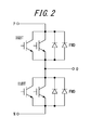
- the above conventional semiconductor device for example as illustrated in FIG. 2 , includes a positive side input terminal P, a negative side input terminal N, and an output terminal O.
- Two Insulated Gate Bipolar Transistors (IGBT) and two Free Wheeling Diodes (FWD) are used in each of the upper and lower arms.
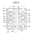
- FIGS. 3 and 4 The layouts of semiconductor devices configured with these methods are illustrated in FIGS. 3 and 4 . Note that in these figures, arrows depicted with solid lines indicate the direction of current when the IGBTs are operating, and arrows depicted with dashed lines indicate the direction of current when the FWDs are operating.
- IGBTs in parallel as a two-chip set are each individually connected by beam leads, as illustrated in FIG. 3 .
- IGBTs 101a and 101b and diodes 102a and 102b fixed to a positive side pattern 104a on an insulating substrate 100 are individually connected by independent beam leads 103a to 103d to an output side pattern 104c on the insulating substrate 100.
- IGBTs 101c and 101d and diodes 102c and 102d fixed to the output side pattern 104c are individually connected by independent beam leads 103e to 103h to a negative side pattern 104b provided on the insulating substrate 100.
- the positive side input terminal P is connected to the positive side pattern 104a at one edge of the insulating substrate 100
- the negative side input terminal N is connected to the negative side pattern 104b at the same edge of the insulating substrate 100
- the output terminal O is connected to the output side pattern 104c at the other edge of the insulating substrate 100.
- connection between each element and pattern is the same as the connection in FIG. 3 , yet the method of wiring the beam leads differs.
- IGBTs 101a and 101b are grouped as a two-chip set on the positive side pattern 104a and are connected to the output side pattern 104c by a beam lead 103i.
- diodes 102a and 102b are grouped as a chip set on the positive side pattern 104a and are connected to the output side pattern 104c by a beam lead 103j.
- IGBTs 101c and 101d are grouped as a two-chip set on the output side pattern 104c and are connected to the negative side pattern 104b by a beam lead 103k.
- diodes 102c and 102d are grouped as a two-chip set on the output side pattern 104c and are connected to the negative side pattern 104b by a beam lead 1031.
- the present invention has been conceived in light of the above problems and provides a semiconductor device with a power module that includes an upper arm and a lower arm each configured by connecting a plurality of power elements and a plurality of rectifying elements in parallel, with the elements wired by beam leads, such that a temperature increase in the beam leads can be suppressed while reducing the number of wiring lines, and such that an increase in manufacturing costs can be suppressed.
- a semiconductor device according to a first aspect of the present invention as recited in claim 1 is a semiconductor device comprising a power module including an upper arm and a lower arm each configured by connecting in parallel a plurality of power elements and a plurality of rectifying elements, current to one arm in the power module flowing through a plurality of separately wired beam leads, a portion of the power elements and a portion of the rectifying elements in the one arm forming a pair and being connected by a common beam lead.
- a semiconductor device is a semiconductor device comprising a power module including an upper arm and a lower arm each configured by connecting in parallel a plurality of power elements and a plurality of rectifying elements identical in number to the power elements, current to one arm in the power module flowing through a plurality of separately wired beam leads, a portion of the power elements and a portion of the rectifying elements, identical in number to the portion of the power elements, in the one arm forming a pair and being connected by a common beam lead.
- a semiconductor device according to a third aspect of the present invention as recited in claim 3 is a semiconductor device comprising a power module including an upper arm and a lower arm each configured by connecting in parallel two power element chips and two rectifying element chips, current to one arm in the power module flowing through a plurality of separately wired beam leads, one of the power element chips and one of the rectifying element chips in the one arm forming a pair and being connected by a common beam lead.
- the semiconductor device recited in claim 1 is a semiconductor device provided with a power module including an upper arm and a lower arm each configured by connecting in parallel a plurality of power elements and a plurality of rectifying elements.
- Current to one arm in the power module flows through a plurality of separately wired beam leads.
- a portion of the power elements and a portion of the rectifying elements in the one arm form a pair and are connected by a common beam lead. Therefore, this pair of elements does not turn ON simultaneously.
- a temperature increase in the beam leads can be suppressed while reducing the number of wiring lines, thereby suppressing an increase in manufacturing costs.
- the semiconductor device recited in claim 2 is a semiconductor device provided with a power module including an upper arm and a lower arm each configured by connecting in parallel a plurality of power elements and a plurality of rectifying elements identical in number to the power elements.
- Current to one arm in the power module flows through a plurality of separately wired beam leads.
- a portion of the power elements and a portion of the rectifying elements, identical in number to the portion of the power elements, in the one arm form a pair and are connected by a common beam lead. Therefore, this pair of elements does not turn ON simultaneously.
- the maximum current flowing through the beam leads can be reduced, and nearly the same amount of current flows in each pair of identical numbers of power elements and rectifying elements, making it possible to prevent current from becoming uneven between beam leads.
- a temperature increase in the beam leads can be suppressed while reducing the number of wiring lines, thereby suppressing an increase in manufacturing costs.
- the semiconductor device recited in claim 3 is a semiconductor device provided with a power module including an upper arm and a lower arm each configured by connecting in parallel two power elements and two rectifying elements.
- Current to one arm in the power module flows through a plurality of separately wired beam leads.
- One of the power elements and one of the rectifying elements in the one arm form a pair and are connected by a common beam lead. Therefore, this pair of elements does not turn ON simultaneously.
- the maximum current flowing through the beam leads can be reduced, and it is possible to prevent current from becoming uneven between beam leads.
- a temperature increase in the beam leads can be suppressed while reducing the number of wiring lines, thereby suppressing an increase in manufacturing costs.
- the semiconductor device of the present embodiment is, for example, used in an inverter that controls power supplied to an electric motor for driving that is mounted in an electric vehicle.
- the semiconductor device of the present embodiment as well is provided with a power module including an upper arm 10 configured by connecting in parallel two IGBTs 1a and 1b and two diodes 2a and 2b.
- the semiconductor device is also provided with a power module including a lower arm 11 configured by connecting in parallel two IGBTs 1c and 1d and two diodes 2c and 2d.
- These power modules are a portion of the above-mentioned inverter.
- An insulating substrate 5 has fixed thereon the following: a rectangular positive side pattern 4a, formed from conducting metal, at the right in FIG. 1 (the upper arm side); a negative side pattern 4b, formed from conducting metal, extending horizontally from the left of FIG. 1 to near the approximate center and then turning downward and extending vertically downward to form an inverted L shape; and an output side pattern 4c, formed from conducting metal, extending from the top edge to the bottom edge in FIG. 1 at approximately the center position of FIG. 1 and then turning to the left (the bottom arm side), extending horizontally to the left edge, and rising vertically from the lower left edge to near the positive side pattern 4b to form a U shape.
- a rectangular positive side pattern 4a formed from conducting metal, at the right in FIG. 1 (the upper arm side)
- a negative side pattern 4b formed from conducting metal, extending horizontally from the left of FIG. 1 to near the approximate center and then turning downward and extending vertically downward to form an inverted L shape
- an output side pattern 4c formed from conducting
- a positive side input terminal P is provided and connected to the positive side pattern 4a.
- a negative side input terminal N is provided and connected to the negative side pattern 4b.
- an output terminal O is provided and connected to the output side pattern 4c.
- the IGBT 1a and the diode 2a for which current flows in opposite directions, form a pair.
- the collector side of the IGBT 1a and the cathode side of the diode 2a are fixed to the positive side pattern 4a provided on the insulating substrate 5.
- the emitter side of the IGBT 1a and the anode side of the diode 2a are grouped and connected to each other by one side of a beam lead 3a, and the other side of the beam lead 3a is connected to the output side pattern 4c provided on the insulating substrate 5.
- the IGBT 1a and the diode 2a are thus made conductive with each other by the beam lead 3a.
- the IGBT 1b and the diode 2b of the upper arm form another pair.
- the collector side of the IGBT 1b and the cathode side of the diode 2b are fixed to the positive side pattern 4a.
- the emitter side of the IGBT 1b and the anode side of the diode 2b are grouped and connected to each other by one side of a beam lead 3b, and the other side of the beam lead 3b is connected to the output side pattern 4c.
- the IGBT 1b and the diode 2b are thus made conductive with each other by the beam lead 3b.
- the IGBT 1c and the diode 2c for which current flows in opposite directions, form a pair.
- the collector side of the IGBT 1c and the cathode side of the diode 2c are fixed to the output side pattern 4c.
- the emitter side of the IGBT 1c and the anode side of the diode 2c are grouped and connected to each other by one side of a beam lead 3c, and the other side of the beam lead 3c is connected to the negative side pattern 4b provided on the insulating substrate 5.
- the IGBT 1c and the diode 2c are thus made conductive with each other by the beam lead 3c.
- the IGBT 1d and the diode 2d of the lower arm form another pair.
- the collector side of the IGBT 1d and the cathode side of the diode 2d are fixed to the output side pattern 4c.
- the emitter side of the IGBT 1d and the anode side of the diode 2d are grouped and connected to each other by one side of a beam lead 3d, and the other side of the beam lead 3d is connected to the negative side pattern 4b.
- the IGBT 1d and the diode 2d are thus made conductive with each other by the beam lead 3d.
- a gate signal for control determined by a control unit (not illustrated) in accordance with the amount of accelerator depression, vehicle speed, or the like, can be applied to the gate of each of the IGBTs 1a to 1d.
- Three combinations that are similar to the combination of the upper arm 10 and the lower arm 11 are provided, and the output terminals thereof are connected to respective coils of a three-phase AC electric motor.
- the IGBTs 1a and 1b of the upper arm 10 and the diodes 2c and 2d of the lower arm 11 form a step-down chopper
- the IGBTs 1c and 1d of the lower arm 11 and the diodes 2a and 2b of the upper arm 10 form a step-up chopper.
- the diodes 2a to 2d are used because, by causing the induced voltage energy generated by the electric motor to flow to the DC power source, the diodes 2a to 2d prevent the terminal voltage of the motor from rising due to the induced voltage, which would cause the IGBTs 1a to 1d to be damaged by overvoltage.
- the diodes 2a and 2b of the upper arm 10 block current from flowing through these diodes 2a and 2b
- the diodes 2c and 2d of the lower arm 11 block current from flowing through these diodes 2c and 2d.
- the IGBTs 1a and 1b of the upper arm 10 are connected individually by different beam leads 3a and 3b, and when the IGBTs 1a and 1b are ON, current does not flow to the diodes 2a and 2b connected to the beam leads 3a and 3b. Therefore, the current flowing through the beam leads 3a and 3b decreases.
- the IGBTs 1c and 1d of the lower arm 11 are connected individually by different beam leads 3c and 3d, and when the IGBTs 1c and 1d are ON, current does not flow to the diodes 2c and 2d connected to the beam leads 3c and 3d. Therefore, the current flowing through the beam leads 3c and 3d decreases.
- arrows depicted with solid lines indicate the direction of current when the IGBTs are operating
- arrows depicted with dashed lines indicate the direction of current when the diodes are operating.
- the power module includes the upper arm 10 and the lower arm 11 each configured by connecting the plurality of IGBTs 1a to 1d and the plurality of diodes 2a to 2d in parallel, and the current in one arm 10 (or 11) flows through the plurality of separately wired beam leads 3a to 3d.
- a portion of the IGBTs 1a and 1b (and/or 1c and 1d) and a portion of the diodes 2a and 2b (and/or 2c and 2d) in the one arm 10 (or 11) form pairs and are connected by common beam leads 3a to 3d. Therefore, in these pairs, the IGBT and diode do not turn ON simultaneously, and hence current does not flow simultaneously to both elements.
- the amount of current flowing through the beam leads 3a to 3d can be suppressed and equalized. Therefore, the beam leads 3a to 3d can be prevented from reaching a high temperature, and the beam leads 3a to 3d need not be made large.
- the beam leads 3a to 3d are fewer in number as compared to when beam leads are individually wired, thus suppressing an increase in manufacturing costs.
- each arm is configured to include two IGBTs and two diodes, yet this embodiment is not limiting.
- the case of one arm being configured with three or more each of the power elements and rectifying elements is included, and the semiconductor device may have a plurality of sets.
- the present invention may also be applied just to a pair of only a portion of the plurality of power elements and rectifying elements in one arm.
Landscapes
- Engineering & Computer Science (AREA)
- Power Engineering (AREA)
- Rectifiers (AREA)
- Inverter Devices (AREA)
Abstract
Description
- The present invention relates to a semiconductor device that includes a power module, having power elements and rectifying elements, in which the elements are wired with beam leads.
- Patent Literature 1 discloses a known example of a conventional semiconductor device such as the one mentioned above.
- This conventional semiconductor device has a paired arm structure formed by a positive side circuit and a negative side circuit. A first metal block is connected to the back side of a plurality of first semiconductor elements (power elements), and a second metal block is connected to the back side of a plurality of second semiconductor elements (rectifying elements). The front side of the first and second semiconductor elements and the first and second metal blocks are connected by a lead frame. The first and second metal blocks form a portion of a main electrode through which principle current flows. The first and second semiconductor elements, the first and second metal blocks, and the lead frame are integrally covered by a package. Within the package, the main electrode and a control electrode that are formed by the lead frame are disposed in nearly the same plane, except for the portion connecting to the first and second semiconductor elements and the first and second metal blocks.
- PTL 1:
JP 2004-22960 A - The above conventional semiconductor device, however, has the problems described below.
- The above conventional semiconductor device, for example as illustrated in
FIG. 2 , includes a positive side input terminal P, a negative side input terminal N, and an output terminal O. Two Insulated Gate Bipolar Transistors (IGBT) and two Free Wheeling Diodes (FWD) are used in each of the upper and lower arms. - Basically, the following two methods are used when wiring such a two-chip parallel-connected power module with beam leads.
- The layouts of semiconductor devices configured with these methods are illustrated in
FIGS. 3 and4 . Note that in these figures, arrows depicted with solid lines indicate the direction of current when the IGBTs are operating, and arrows depicted with dashed lines indicate the direction of current when the FWDs are operating. - To begin with, in the first method, IGBTs in parallel as a two-chip set are each individually connected by beam leads, as illustrated in
FIG. 3 . - As illustrated in the same figure, in the upper arm, IGBTs 101a and 101b and
diodes positive side pattern 104a on aninsulating substrate 100 are individually connected by independent beam leads 103a to 103d to anoutput side pattern 104c on theinsulating substrate 100. - On the other hand, in the lower arm,
IGBTs diodes output side pattern 104c are individually connected by independent beam leads 103e to 103h to anegative side pattern 104b provided on theinsulating substrate 100. - The positive side input terminal P is connected to the
positive side pattern 104a at one edge of theinsulating substrate 100, the negative side input terminal N is connected to thenegative side pattern 104b at the same edge of theinsulating substrate 100, and the output terminal O is connected to theoutput side pattern 104c at the other edge of theinsulating substrate 100. - By thus wiring each element independently with an independent beam lead, the number of wiring lines and production steps grows large, leading to the problem of increased manufacturing costs.
- In the second method, as illustrated in
FIG. 4 , the connection between each element and pattern is the same as the connection inFIG. 3 , yet the method of wiring the beam leads differs. - Specifically, in the upper arm, IGBTs 101a and 101b are grouped as a two-chip set on the
positive side pattern 104a and are connected to theoutput side pattern 104c by a beam lead 103i. Similarly,diodes positive side pattern 104a and are connected to theoutput side pattern 104c by a beam lead 103j. - On the other hand, in the lower arm,
IGBTs output side pattern 104c and are connected to thenegative side pattern 104b by abeam lead 103k. Similarly,diodes output side pattern 104c and are connected to thenegative side pattern 104b by abeam lead 1031. - With this configuration, however, current flows simultaneously to a plurality of IGBTs or diodes connected by the same beam lead, causing the problem of the beam leads reaching a high temperature due to the high amount of current.
- To avoid this problem, the beam leads need to be thickened, causing the problem of increased manufacturing costs.
- The present invention has been conceived in light of the above problems and provides a semiconductor device with a power module that includes an upper arm and a lower arm each configured by connecting a plurality of power elements and a plurality of rectifying elements in parallel, with the elements wired by beam leads, such that a temperature increase in the beam leads can be suppressed while reducing the number of wiring lines, and such that an increase in manufacturing costs can be suppressed.
- A semiconductor device according to a first aspect of the present invention as recited in claim 1 is a semiconductor device comprising a power module including an upper arm and a lower arm each configured by connecting in parallel a plurality of power elements and a plurality of rectifying elements, current to one arm in the power module flowing through a plurality of separately wired beam leads, a portion of the power elements and a portion of the rectifying elements in the one arm forming a pair and being connected by a common beam lead.
- A semiconductor device according to a second aspect of the present invention as recited in claim 2 is a semiconductor device comprising a power module including an upper arm and a lower arm each configured by connecting in parallel a plurality of power elements and a plurality of rectifying elements identical in number to the power elements, current to one arm in the power module flowing through a plurality of separately wired beam leads, a portion of the power elements and a portion of the rectifying elements, identical in number to the portion of the power elements, in the one arm forming a pair and being connected by a common beam lead.
- A semiconductor device according to a third aspect of the present invention as recited in claim 3 is a semiconductor device comprising a power module including an upper arm and a lower arm each configured by connecting in parallel two power element chips and two rectifying element chips, current to one arm in the power module flowing through a plurality of separately wired beam leads, one of the power element chips and one of the rectifying element chips in the one arm forming a pair and being connected by a common beam lead.
- The semiconductor device recited in claim 1 is a semiconductor device provided with a power module including an upper arm and a lower arm each configured by connecting in parallel a plurality of power elements and a plurality of rectifying elements. Current to one arm in the power module flows through a plurality of separately wired beam leads. A portion of the power elements and a portion of the rectifying elements in the one arm form a pair and are connected by a common beam lead. Therefore, this pair of elements does not turn ON simultaneously.
- As a result, the maximum current flowing through the beam leads can be reduced.
- Accordingly, a temperature increase in the beam leads can be suppressed while reducing the number of wiring lines, thereby suppressing an increase in manufacturing costs.
- The semiconductor device recited in claim 2 is a semiconductor device provided with a power module including an upper arm and a lower arm each configured by connecting in parallel a plurality of power elements and a plurality of rectifying elements identical in number to the power elements. Current to one arm in the power module flows through a plurality of separately wired beam leads. A portion of the power elements and a portion of the rectifying elements, identical in number to the portion of the power elements, in the one arm form a pair and are connected by a common beam lead. Therefore, this pair of elements does not turn ON simultaneously.
- As a result, the maximum current flowing through the beam leads can be reduced, and nearly the same amount of current flows in each pair of identical numbers of power elements and rectifying elements, making it possible to prevent current from becoming uneven between beam leads.
- Accordingly, a temperature increase in the beam leads can be suppressed while reducing the number of wiring lines, thereby suppressing an increase in manufacturing costs.
- The semiconductor device recited in claim 3 is a semiconductor device provided with a power module including an upper arm and a lower arm each configured by connecting in parallel two power elements and two rectifying elements. Current to one arm in the power module flows through a plurality of separately wired beam leads. One of the power elements and one of the rectifying elements in the one arm form a pair and are connected by a common beam lead. Therefore, this pair of elements does not turn ON simultaneously.
- As a result, the maximum current flowing through the beam leads can be reduced, and it is possible to prevent current from becoming uneven between beam leads.
- Accordingly, in a power module with the above two-chip configuration as well, a temperature increase in the beam leads can be suppressed while reducing the number of wiring lines, thereby suppressing an increase in manufacturing costs.
- The present invention will be further described below with reference to the accompanying drawings, wherein:
-
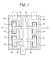
FIG. 1 illustrates the layout of power elements, rectifying elements, and the like, as well as the flow of current therein, in a semiconductor device according to an embodiment of the present invention; -
FIG. 2 is a circuit diagram of a semiconductor device according to a conventional technique, in which two-chip sets of power elements are connected by beam leads; -
FIG. 3 illustrates the layout and the direction of current in a semiconductor device according to a conventional technique, in which each element in a two-chip set of power elements is individually connected by a beam lead; and -
FIG. 4 illustrates the layout and the direction of current in a semiconductor device according to a conventional technique, in which a two-chip set of power elements is collectively connected by one beam lead. - The following describes embodiments of the present invention in detail, based on the embodiment illustrated in the drawings.
- First, the overall configuration of a semiconductor device according to the present embodiment is described.
- The semiconductor device of the present embodiment is, for example, used in an inverter that controls power supplied to an electric motor for driving that is mounted in an electric vehicle.
- As illustrated in
FIG. 1 , the semiconductor device of the present embodiment as well is provided with a power module including anupper arm 10 configured by connecting in parallel twoIGBTs diodes lower arm 11 configured by connecting in parallel twoIGBTs diodes - An insulating
substrate 5 has fixed thereon the following: a rectangularpositive side pattern 4a, formed from conducting metal, at the right inFIG. 1 (the upper arm side); anegative side pattern 4b, formed from conducting metal, extending horizontally from the left ofFIG. 1 to near the approximate center and then turning downward and extending vertically downward to form an inverted L shape; and anoutput side pattern 4c, formed from conducting metal, extending from the top edge to the bottom edge inFIG. 1 at approximately the center position ofFIG. 1 and then turning to the left (the bottom arm side), extending horizontally to the left edge, and rising vertically from the lower left edge to near thepositive side pattern 4b to form a U shape. - At one edge of the insulating substrate 5 (at the top edge in
FIG. 1 ), a positive side input terminal P is provided and connected to thepositive side pattern 4a. At the same edge of the insulatingsubstrate 5, a negative side input terminal N is provided and connected to thenegative side pattern 4b. At the other edge of the insulating substrate 5 (at the bottom edge inFIG. 1 ), an output terminal O is provided and connected to theoutput side pattern 4c. - At the upper arm side, the
IGBT 1a and thediode 2a, for which current flows in opposite directions, form a pair. For example, in the case of theIGBT 1a being an n-channel type, the collector side of theIGBT 1a and the cathode side of thediode 2a are fixed to thepositive side pattern 4a provided on the insulatingsubstrate 5. The emitter side of theIGBT 1a and the anode side of thediode 2a are grouped and connected to each other by one side of abeam lead 3a, and the other side of thebeam lead 3a is connected to theoutput side pattern 4c provided on the insulatingsubstrate 5. TheIGBT 1a and thediode 2a are thus made conductive with each other by thebeam lead 3a. - Similarly, the
IGBT 1b and thediode 2b of the upper arm, for which current flows in opposite directions, form another pair. For example, in the case of theIGBT 1b being an n-channel type, the collector side of theIGBT 1b and the cathode side of thediode 2b are fixed to thepositive side pattern 4a. The emitter side of theIGBT 1b and the anode side of thediode 2b are grouped and connected to each other by one side of abeam lead 3b, and the other side of thebeam lead 3b is connected to theoutput side pattern 4c. TheIGBT 1b and thediode 2b are thus made conductive with each other by thebeam lead 3b. - On the other hand, at the lower arm side, the
IGBT 1c and thediode 2c, for which current flows in opposite directions, form a pair. For example, in the case of theIGBT 1c being an n-channel type, the collector side of theIGBT 1c and the cathode side of thediode 2c are fixed to theoutput side pattern 4c. The emitter side of theIGBT 1c and the anode side of thediode 2c are grouped and connected to each other by one side of abeam lead 3c, and the other side of thebeam lead 3c is connected to thenegative side pattern 4b provided on the insulatingsubstrate 5. TheIGBT 1c and thediode 2c are thus made conductive with each other by thebeam lead 3c. - Similarly, the
IGBT 1d and thediode 2d of the lower arm, for which current flows in opposite directions, form another pair. For example, in the case of theIGBT 1d being an n-channel type, the collector side of theIGBT 1d and the cathode side of thediode 2d are fixed to theoutput side pattern 4c. The emitter side of theIGBT 1d and the anode side of thediode 2d are grouped and connected to each other by one side of abeam lead 3d, and the other side of thebeam lead 3d is connected to thenegative side pattern 4b. TheIGBT 1d and thediode 2d are thus made conductive with each other by thebeam lead 3d. - While not illustrated, a gate signal for control, determined by a control unit (not illustrated) in accordance with the amount of accelerator depression, vehicle speed, or the like, can be applied to the gate of each of the IGBTs 1a to 1d.
- Three combinations that are similar to the combination of the
upper arm 10 and thelower arm 11 are provided, and the output terminals thereof are connected to respective coils of a three-phase AC electric motor. - Next, the operations of the inverter that is a semiconductor device with the above-described configuration are described.
- In the above-described semiconductor device, the
IGBTs upper arm 10 and thediodes lower arm 11 form a step-down chopper, and theIGBTs lower arm 11 and thediodes upper arm 10 form a step-up chopper. - By complementary switching of the
IGBTs lower arms - In other words, by turning the
IGBTs upper arm 10 ON and theIGBTs lower arm 11 OFF, positive reactor current flows through theIGBTs upper arm 10 into the electric motor coil connected to the output terminal O. Conversely, by turning theIGBTs lower arm 11 ON and theIGBTs upper arm 10 OFF, negative reactor current flows through theIGBTs - The
diodes 2a to 2d are used because, by causing the induced voltage energy generated by the electric motor to flow to the DC power source, thediodes 2a to 2d prevent the terminal voltage of the motor from rising due to the induced voltage, which would cause the IGBTs 1a to 1d to be damaged by overvoltage. - Furthermore, in the former case mentioned above in which positive reactor current flows, the
diodes upper arm 10 block current from flowing through thesediodes diodes lower arm 11 block current from flowing through thesediodes - Accordingly, current does not flow simultaneously through both the
IGBTs diodes upper arm 10, and similarly, current does not flow simultaneously through both theIGBTs diodes lower arm 11. - The
IGBTs upper arm 10 are connected individually by different beam leads 3a and 3b, and when theIGBTs diodes - Similarly, the
IGBTs lower arm 11 are connected individually by different beam leads 3c and 3d, and when theIGBTs diodes - Note that in
FIG. 1 , arrows depicted with solid lines indicate the direction of current when the IGBTs are operating, and arrows depicted with dashed lines indicate the direction of current when the diodes are operating. - As is clear from the above description, in the semiconductor device of the present embodiment, the power module includes the
upper arm 10 and thelower arm 11 each configured by connecting the plurality ofIGBTs 1a to 1d and the plurality ofdiodes 2a to 2d in parallel, and the current in one arm 10 (or 11) flows through the plurality of separately wired beam leads 3a to 3d. At this time, in the semiconductor device, a portion of theIGBTs diodes - In other words, only one chip's worth (either the IGBT or the diode in the pair) of current flows simultaneously through the beam leads 3a to 3d.
- Accordingly, the amount of current flowing through the beam leads 3a to 3d can be suppressed and equalized. Therefore, the beam leads 3a to 3d can be prevented from reaching a high temperature, and the beam leads 3a to 3d need not be made large.
- Furthermore, the beam leads 3a to 3d are fewer in number as compared to when beam leads are individually wired, thus suppressing an increase in manufacturing costs.
- The present invention has been described based on the above embodiments, yet the present invention is not limited to these embodiments and includes any design modification or the like within the spirit and scope of the present invention.
- For example, in the embodiment, each arm is configured to include two IGBTs and two diodes, yet this embodiment is not limiting. The case of one arm being configured with three or more each of the power elements and rectifying elements is included, and the semiconductor device may have a plurality of sets.
- The present invention may also be applied just to a pair of only a portion of the plurality of power elements and rectifying elements in one arm.
-
- 1a, 1b: IGBT (power element) at upper arm side
- 1c, 1d: IGBT (power element) at lower arm side
- 2a, 2b: Diode (rectifying element) at upper arm side
- 2c, 2d: Diode (rectifying element) at lower arm side
- 3a to 3d: Beam lead
- 4a: Positive side pattern
- 4b: Negative side pattern
- 4c: Output side pattern
- 5: Insulating substrate
- 10: Upper arm
- 11: Lower arm
- N: Negative side input terminal
- P: Positive side input terminal
- O: Output terminal
Claims (3)
- A semiconductor device comprising a power module including an upper arm and a lower arm each configured by connecting in parallel a plurality of power elements and a plurality of rectifying elements, current to one arm in the power module flowing through a plurality of separately wired beam leads,
a portion of the power elements and a portion of the rectifying elements in the one arm forming a pair and being connected by a common beam lead. - A semiconductor device comprising a power module including an upper arm and a lower arm each configured by connecting in parallel a plurality of power elements and a plurality of rectifying elements identical in number to the power elements, current to one arm in the power module flowing through a plurality of separately wired beam leads,
a portion of the power elements and a portion of the rectifying elements, identical in number to the portion of the power elements, in the one arm forming a pair and being connected by a common beam lead. - A semiconductor device comprising a power module including an upper arm and a lower arm each configured by connecting in parallel two power element chips and two rectifying element chips, current to one arm in the power module flowing through a plurality of separately wired beam leads,
one of the power element chips and one of the rectifying element chips in the one arm forming a pair and being connected by a common beam lead.
Applications Claiming Priority (2)
| Application Number | Priority Date | Filing Date | Title |
|---|---|---|---|
| JP2012200305A JP2014056920A (en) | 2012-09-12 | 2012-09-12 | Semiconductor device |
| PCT/JP2013/003117 WO2014041722A1 (en) | 2012-09-12 | 2013-05-16 | Semiconductor device |
Publications (2)
| Publication Number | Publication Date |
|---|---|
| EP2897165A1 true EP2897165A1 (en) | 2015-07-22 |
| EP2897165A4 EP2897165A4 (en) | 2016-01-06 |
Family
ID=50277869
Family Applications (1)
| Application Number | Title | Priority Date | Filing Date |
|---|---|---|---|
| EP13837869.0A Withdrawn EP2897165A4 (en) | 2012-09-12 | 2013-05-16 | SEMICONDUCTOR DEVICE |
Country Status (5)
| Country | Link |
|---|---|
| US (1) | US9607931B2 (en) |
| EP (1) | EP2897165A4 (en) |
| JP (1) | JP2014056920A (en) |
| CN (1) | CN104603938B (en) |
| WO (1) | WO2014041722A1 (en) |
Cited By (1)
| Publication number | Priority date | Publication date | Assignee | Title |
|---|---|---|---|---|
| US9905494B2 (en) | 2015-04-27 | 2018-02-27 | Fuji Electric Co., Ltd. | Semiconductor device |
Families Citing this family (8)
| Publication number | Priority date | Publication date | Assignee | Title |
|---|---|---|---|---|
| CN106415834B (en) * | 2014-11-28 | 2019-09-13 | 富士电机株式会社 | semiconductor device |
| JP5887007B1 (en) * | 2015-07-07 | 2016-03-16 | カルソニックカンセイ株式会社 | Power semiconductor device |
| JP6599736B2 (en) * | 2015-11-20 | 2019-10-30 | 株式会社三社電機製作所 | Semiconductor module |
| JP6760156B2 (en) * | 2017-03-20 | 2020-09-23 | 株式会社デンソー | Power converter |
| CN111886695B (en) | 2018-10-05 | 2024-11-01 | 富士电机株式会社 | Semiconductor device, semiconductor module and vehicle |
| DE102019206820A1 (en) * | 2019-05-10 | 2020-11-12 | Robert Bosch Gmbh | Semiconductor power module |
| DE102019206822A1 (en) * | 2019-05-10 | 2020-11-12 | Robert Bosch Gmbh | Semiconductor power module |
| JP6939932B1 (en) * | 2020-03-12 | 2021-09-22 | 住友電気工業株式会社 | Semiconductor device |
Family Cites Families (11)
| Publication number | Priority date | Publication date | Assignee | Title |
|---|---|---|---|---|
| JPH0480065U (en) * | 1990-11-27 | 1992-07-13 | ||
| JP4220731B2 (en) | 2002-06-19 | 2009-02-04 | 三菱電機株式会社 | Power semiconductor device |
| JP2004273749A (en) * | 2003-03-07 | 2004-09-30 | Fuji Electric Fa Components & Systems Co Ltd | Semiconductor power module |
| JP4566678B2 (en) * | 2004-10-04 | 2010-10-20 | 日立オートモティブシステムズ株式会社 | Power module |
| JP4603956B2 (en) * | 2005-08-26 | 2010-12-22 | 日立オートモティブシステムズ株式会社 | Power converter |
| JP2008086099A (en) * | 2006-09-27 | 2008-04-10 | Honda Motor Co Ltd | Inverter device |
| JP4858238B2 (en) * | 2007-03-05 | 2012-01-18 | 富士電機株式会社 | Laser welding member and semiconductor device using the same |
| JP4757815B2 (en) * | 2007-03-05 | 2011-08-24 | 本田技研工業株式会社 | Electric motor control device and vehicle |
| US7570008B2 (en) * | 2007-07-30 | 2009-08-04 | Hitachi, Ltd. | Power module, power converter, and electric machine system for mounting in vehicle |
| JP2009159184A (en) * | 2007-12-26 | 2009-07-16 | Hitachi Ltd | CIRCUIT DEVICE HAVING FREE WHEEL DIODE, CIRCUIT DEVICE USING DIODE AND POWER CONVERTER USING SAME |
| US9673283B2 (en) * | 2011-05-06 | 2017-06-06 | Cree, Inc. | Power module for supporting high current densities |
-
2012
- 2012-09-12 JP JP2012200305A patent/JP2014056920A/en active Pending
-
2013
- 2013-05-16 US US14/421,636 patent/US9607931B2/en not_active Expired - Fee Related
- 2013-05-16 EP EP13837869.0A patent/EP2897165A4/en not_active Withdrawn
- 2013-05-16 CN CN201380046664.5A patent/CN104603938B/en not_active Expired - Fee Related
- 2013-05-16 WO PCT/JP2013/003117 patent/WO2014041722A1/en not_active Ceased
Cited By (1)
| Publication number | Priority date | Publication date | Assignee | Title |
|---|---|---|---|---|
| US9905494B2 (en) | 2015-04-27 | 2018-02-27 | Fuji Electric Co., Ltd. | Semiconductor device |
Also Published As
| Publication number | Publication date |
|---|---|
| CN104603938B (en) | 2017-09-19 |
| CN104603938A (en) | 2015-05-06 |
| EP2897165A4 (en) | 2016-01-06 |
| JP2014056920A (en) | 2014-03-27 |
| WO2014041722A1 (en) | 2014-03-20 |
| US9607931B2 (en) | 2017-03-28 |
| US20150235923A1 (en) | 2015-08-20 |
Similar Documents
| Publication | Publication Date | Title |
|---|---|---|
| US9607931B2 (en) | Semiconductor device for suppressing a temperature increase in beam leads | |
| JP7153649B2 (en) | Power semiconductor modules with low gate path inductance | |
| CN110495087B (en) | Semiconductor module and power conversion device | |
| JP6196853B2 (en) | 3 level converter half bridge | |
| JP2019029457A (en) | Semiconductor module | |
| JP2010104204A (en) | Power converter | |
| JP2014217270A (en) | Half bridge for 3-level power conversion device | |
| EP3442108A1 (en) | Multilevel power converter | |
| US11710685B2 (en) | Semiconductor module and power conversion device | |
| JP2013162690A (en) | Vvvf inverter and vehicle controller | |
| CN112204733A (en) | Semiconductor module and power conversion device | |
| WO2025119364A1 (en) | Power semiconductor module, half-bridge power module, and vehicle | |
| CN109755229A (en) | A kind of IGBT module | |
| CN105097738A (en) | Semiconductor device | |
| US10186978B2 (en) | Modular power conversion semiconductor device | |
| JP2009148077A (en) | Voltage-driven semiconductor module and power converter using same | |
| WO2020078082A1 (en) | Different-edge-connecting power electrode assembly and power module | |
| JP2017162884A (en) | Semiconductor device | |
| CN105374811A (en) | a power module | |
| US10930616B2 (en) | Semiconductor module, method for manufacturing semiconductor module, and power conversion apparatus | |
| CN105374809A (en) | Power module | |
| CN205211749U (en) | Power module | |
| JP6362959B2 (en) | Power conversion circuit, manufacturing method thereof, and power conditioner | |
| CN109560066A (en) | A kind of power module with gap bridge conductive layer | |
| CN109585436A (en) | A kind of power module of interspersed branch's layout |
Legal Events
| Date | Code | Title | Description |
|---|---|---|---|
| PUAI | Public reference made under article 153(3) epc to a published international application that has entered the european phase |
Free format text: ORIGINAL CODE: 0009012 |
|
| 17P | Request for examination filed |
Effective date: 20150305 |
|
| AK | Designated contracting states |
Kind code of ref document: A1 Designated state(s): AL AT BE BG CH CY CZ DE DK EE ES FI FR GB GR HR HU IE IS IT LI LT LU LV MC MK MT NL NO PL PT RO RS SE SI SK SM TR |
|
| AX | Request for extension of the european patent |
Extension state: BA ME |
|
| DAX | Request for extension of the european patent (deleted) | ||
| RIN1 | Information on inventor provided before grant (corrected) |
Inventor name: YASUDA, HIROKI |
|
| RA4 | Supplementary search report drawn up and despatched (corrected) |
Effective date: 20151203 |
|
| RIC1 | Information provided on ipc code assigned before grant |
Ipc: H02M 7/48 20070101ALI20151127BHEP Ipc: H01L 23/48 20060101AFI20151127BHEP Ipc: H01L 25/07 20060101ALI20151127BHEP Ipc: H01L 25/18 20060101ALI20151127BHEP |
|
| STAA | Information on the status of an ep patent application or granted ep patent |
Free format text: STATUS: THE APPLICATION HAS BEEN WITHDRAWN |
|
| 18W | Application withdrawn |
Effective date: 20190415 |