EP2897163A1 - Semiconductor device and method for manufacturing semiconductor device - Google Patents
Semiconductor device and method for manufacturing semiconductor device Download PDFInfo
- Publication number
- EP2897163A1 EP2897163A1 EP15150271.3A EP15150271A EP2897163A1 EP 2897163 A1 EP2897163 A1 EP 2897163A1 EP 15150271 A EP15150271 A EP 15150271A EP 2897163 A1 EP2897163 A1 EP 2897163A1
- Authority
- EP
- European Patent Office
- Prior art keywords
- layer
- insulation layer
- semiconductor element
- semiconductor device
- external connection
- Prior art date
- Legal status (The legal status is an assumption and is not a legal conclusion. Google has not performed a legal analysis and makes no representation as to the accuracy of the status listed.)
- Granted
Links
Images




Classifications
-
- H—ELECTRICITY
- H10—SEMICONDUCTOR DEVICES; ELECTRIC SOLID-STATE DEVICES NOT OTHERWISE PROVIDED FOR
- H10W—GENERIC PACKAGES, INTERCONNECTIONS, CONNECTORS OR OTHER CONSTRUCTIONAL DETAILS OF DEVICES COVERED BY CLASS H10
- H10W74/00—Encapsulations, e.g. protective coatings
- H10W74/01—Manufacture or treatment
- H10W74/019—Manufacture or treatment using temporary auxiliary substrates
-
- H—ELECTRICITY
- H10—SEMICONDUCTOR DEVICES; ELECTRIC SOLID-STATE DEVICES NOT OTHERWISE PROVIDED FOR
- H10W—GENERIC PACKAGES, INTERCONNECTIONS, CONNECTORS OR OTHER CONSTRUCTIONAL DETAILS OF DEVICES COVERED BY CLASS H10
- H10W74/00—Encapsulations, e.g. protective coatings
- H10W74/10—Encapsulations, e.g. protective coatings characterised by their shape or disposition
- H10W74/111—Encapsulations, e.g. protective coatings characterised by their shape or disposition the semiconductor body being completely enclosed
- H10W74/114—Encapsulations, e.g. protective coatings characterised by their shape or disposition the semiconductor body being completely enclosed by a substrate and the encapsulations
- H10W74/117—Encapsulations, e.g. protective coatings characterised by their shape or disposition the semiconductor body being completely enclosed by a substrate and the encapsulations the substrate having spherical bumps for external connection
-
- H—ELECTRICITY
- H10—SEMICONDUCTOR DEVICES; ELECTRIC SOLID-STATE DEVICES NOT OTHERWISE PROVIDED FOR
- H10W—GENERIC PACKAGES, INTERCONNECTIONS, CONNECTORS OR OTHER CONSTRUCTIONAL DETAILS OF DEVICES COVERED BY CLASS H10
- H10W90/00—Package configurations
-
- H—ELECTRICITY
- H10—SEMICONDUCTOR DEVICES; ELECTRIC SOLID-STATE DEVICES NOT OTHERWISE PROVIDED FOR
- H10W—GENERIC PACKAGES, INTERCONNECTIONS, CONNECTORS OR OTHER CONSTRUCTIONAL DETAILS OF DEVICES COVERED BY CLASS H10
- H10W70/00—Package substrates; Interposers; Redistribution layers [RDL]
- H10W70/60—Insulating or insulated package substrates; Interposers; Redistribution layers
- H10W70/62—Insulating or insulated package substrates; Interposers; Redistribution layers characterised by their interconnections
- H10W70/63—Vias, e.g. via plugs
-
- H—ELECTRICITY
- H10—SEMICONDUCTOR DEVICES; ELECTRIC SOLID-STATE DEVICES NOT OTHERWISE PROVIDED FOR
- H10W—GENERIC PACKAGES, INTERCONNECTIONS, CONNECTORS OR OTHER CONSTRUCTIONAL DETAILS OF DEVICES COVERED BY CLASS H10
- H10W72/00—Interconnections or connectors in packages
- H10W72/01—Manufacture or treatment
- H10W72/0198—Manufacture or treatment batch processes
-
- H—ELECTRICITY
- H10—SEMICONDUCTOR DEVICES; ELECTRIC SOLID-STATE DEVICES NOT OTHERWISE PROVIDED FOR
- H10W—GENERIC PACKAGES, INTERCONNECTIONS, CONNECTORS OR OTHER CONSTRUCTIONAL DETAILS OF DEVICES COVERED BY CLASS H10
- H10W72/00—Interconnections or connectors in packages
- H10W72/071—Connecting or disconnecting
- H10W72/072—Connecting or disconnecting of bump connectors
-
- H—ELECTRICITY
- H10—SEMICONDUCTOR DEVICES; ELECTRIC SOLID-STATE DEVICES NOT OTHERWISE PROVIDED FOR
- H10W—GENERIC PACKAGES, INTERCONNECTIONS, CONNECTORS OR OTHER CONSTRUCTIONAL DETAILS OF DEVICES COVERED BY CLASS H10
- H10W72/00—Interconnections or connectors in packages
- H10W72/071—Connecting or disconnecting
- H10W72/072—Connecting or disconnecting of bump connectors
- H10W72/07202—Connecting or disconnecting of bump connectors using auxiliary members
- H10W72/07204—Connecting or disconnecting of bump connectors using auxiliary members using temporary auxiliary members, e.g. sacrificial coatings
- H10W72/07207—Temporary substrates, e.g. removable substrates
-
- H—ELECTRICITY
- H10—SEMICONDUCTOR DEVICES; ELECTRIC SOLID-STATE DEVICES NOT OTHERWISE PROVIDED FOR
- H10W—GENERIC PACKAGES, INTERCONNECTIONS, CONNECTORS OR OTHER CONSTRUCTIONAL DETAILS OF DEVICES COVERED BY CLASS H10
- H10W72/00—Interconnections or connectors in packages
- H10W72/071—Connecting or disconnecting
- H10W72/072—Connecting or disconnecting of bump connectors
- H10W72/07231—Techniques
- H10W72/07232—Compression bonding, e.g. thermocompression bonding
-
- H—ELECTRICITY
- H10—SEMICONDUCTOR DEVICES; ELECTRIC SOLID-STATE DEVICES NOT OTHERWISE PROVIDED FOR
- H10W—GENERIC PACKAGES, INTERCONNECTIONS, CONNECTORS OR OTHER CONSTRUCTIONAL DETAILS OF DEVICES COVERED BY CLASS H10
- H10W72/00—Interconnections or connectors in packages
- H10W72/071—Connecting or disconnecting
- H10W72/073—Connecting or disconnecting of die-attach connectors
-
- H—ELECTRICITY
- H10—SEMICONDUCTOR DEVICES; ELECTRIC SOLID-STATE DEVICES NOT OTHERWISE PROVIDED FOR
- H10W—GENERIC PACKAGES, INTERCONNECTIONS, CONNECTORS OR OTHER CONSTRUCTIONAL DETAILS OF DEVICES COVERED BY CLASS H10
- H10W72/00—Interconnections or connectors in packages
- H10W72/071—Connecting or disconnecting
- H10W72/073—Connecting or disconnecting of die-attach connectors
- H10W72/07302—Connecting or disconnecting of die-attach connectors using an auxiliary member
- H10W72/07304—Connecting or disconnecting of die-attach connectors using an auxiliary member the auxiliary member being temporary, e.g. a sacrificial coating
- H10W72/07307—Connecting or disconnecting of die-attach connectors using an auxiliary member the auxiliary member being temporary, e.g. a sacrificial coating the auxiliary member being a temporary substrate, e.g. a removable substrate
-
- H—ELECTRICITY
- H10—SEMICONDUCTOR DEVICES; ELECTRIC SOLID-STATE DEVICES NOT OTHERWISE PROVIDED FOR
- H10W—GENERIC PACKAGES, INTERCONNECTIONS, CONNECTORS OR OTHER CONSTRUCTIONAL DETAILS OF DEVICES COVERED BY CLASS H10
- H10W72/00—Interconnections or connectors in packages
- H10W72/20—Bump connectors, e.g. solder bumps or copper pillars; Dummy bumps; Thermal bumps
- H10W72/241—Dispositions, e.g. layouts
-
- H—ELECTRICITY
- H10—SEMICONDUCTOR DEVICES; ELECTRIC SOLID-STATE DEVICES NOT OTHERWISE PROVIDED FOR
- H10W—GENERIC PACKAGES, INTERCONNECTIONS, CONNECTORS OR OTHER CONSTRUCTIONAL DETAILS OF DEVICES COVERED BY CLASS H10
- H10W72/00—Interconnections or connectors in packages
- H10W72/20—Bump connectors, e.g. solder bumps or copper pillars; Dummy bumps; Thermal bumps
- H10W72/251—Materials
- H10W72/252—Materials comprising solid metals or solid metalloids, e.g. PbSn, Ag or Cu
-
- H—ELECTRICITY
- H10—SEMICONDUCTOR DEVICES; ELECTRIC SOLID-STATE DEVICES NOT OTHERWISE PROVIDED FOR
- H10W—GENERIC PACKAGES, INTERCONNECTIONS, CONNECTORS OR OTHER CONSTRUCTIONAL DETAILS OF DEVICES COVERED BY CLASS H10
- H10W72/00—Interconnections or connectors in packages
- H10W72/20—Bump connectors, e.g. solder bumps or copper pillars; Dummy bumps; Thermal bumps
- H10W72/261—Functions other than electrical connecting
-
- H—ELECTRICITY
- H10—SEMICONDUCTOR DEVICES; ELECTRIC SOLID-STATE DEVICES NOT OTHERWISE PROVIDED FOR
- H10W—GENERIC PACKAGES, INTERCONNECTIONS, CONNECTORS OR OTHER CONSTRUCTIONAL DETAILS OF DEVICES COVERED BY CLASS H10
- H10W72/00—Interconnections or connectors in packages
- H10W72/50—Bond wires
- H10W72/551—Materials of bond wires
- H10W72/552—Materials of bond wires comprising metals or metalloids, e.g. silver
- H10W72/5522—Materials of bond wires comprising metals or metalloids, e.g. silver comprising gold [Au]
-
- H—ELECTRICITY
- H10—SEMICONDUCTOR DEVICES; ELECTRIC SOLID-STATE DEVICES NOT OTHERWISE PROVIDED FOR
- H10W—GENERIC PACKAGES, INTERCONNECTIONS, CONNECTORS OR OTHER CONSTRUCTIONAL DETAILS OF DEVICES COVERED BY CLASS H10
- H10W72/00—Interconnections or connectors in packages
- H10W72/851—Dispositions of multiple connectors or interconnections
- H10W72/874—On different surfaces
- H10W72/884—Die-attach connectors and bond wires
-
- H—ELECTRICITY
- H10—SEMICONDUCTOR DEVICES; ELECTRIC SOLID-STATE DEVICES NOT OTHERWISE PROVIDED FOR
- H10W—GENERIC PACKAGES, INTERCONNECTIONS, CONNECTORS OR OTHER CONSTRUCTIONAL DETAILS OF DEVICES COVERED BY CLASS H10
- H10W74/00—Encapsulations, e.g. protective coatings
-
- H—ELECTRICITY
- H10—SEMICONDUCTOR DEVICES; ELECTRIC SOLID-STATE DEVICES NOT OTHERWISE PROVIDED FOR
- H10W—GENERIC PACKAGES, INTERCONNECTIONS, CONNECTORS OR OTHER CONSTRUCTIONAL DETAILS OF DEVICES COVERED BY CLASS H10
- H10W74/00—Encapsulations, e.g. protective coatings
- H10W74/10—Encapsulations, e.g. protective coatings characterised by their shape or disposition
-
- H—ELECTRICITY
- H10—SEMICONDUCTOR DEVICES; ELECTRIC SOLID-STATE DEVICES NOT OTHERWISE PROVIDED FOR
- H10W—GENERIC PACKAGES, INTERCONNECTIONS, CONNECTORS OR OTHER CONSTRUCTIONAL DETAILS OF DEVICES COVERED BY CLASS H10
- H10W74/00—Encapsulations, e.g. protective coatings
- H10W74/10—Encapsulations, e.g. protective coatings characterised by their shape or disposition
- H10W74/15—Encapsulations, e.g. protective coatings characterised by their shape or disposition on active surfaces of flip-chip devices, e.g. underfills
-
- H—ELECTRICITY
- H10—SEMICONDUCTOR DEVICES; ELECTRIC SOLID-STATE DEVICES NOT OTHERWISE PROVIDED FOR
- H10W—GENERIC PACKAGES, INTERCONNECTIONS, CONNECTORS OR OTHER CONSTRUCTIONAL DETAILS OF DEVICES COVERED BY CLASS H10
- H10W90/00—Package configurations
- H10W90/701—Package configurations characterised by the relative positions of pads or connectors relative to package parts
- H10W90/721—Package configurations characterised by the relative positions of pads or connectors relative to package parts of bump connectors
- H10W90/724—Package configurations characterised by the relative positions of pads or connectors relative to package parts of bump connectors between a chip and a stacked insulating package substrate, interposer or RDL
-
- H—ELECTRICITY
- H10—SEMICONDUCTOR DEVICES; ELECTRIC SOLID-STATE DEVICES NOT OTHERWISE PROVIDED FOR
- H10W—GENERIC PACKAGES, INTERCONNECTIONS, CONNECTORS OR OTHER CONSTRUCTIONAL DETAILS OF DEVICES COVERED BY CLASS H10
- H10W90/00—Package configurations
- H10W90/701—Package configurations characterised by the relative positions of pads or connectors relative to package parts
- H10W90/731—Package configurations characterised by the relative positions of pads or connectors relative to package parts of die-attach connectors
- H10W90/734—Package configurations characterised by the relative positions of pads or connectors relative to package parts of die-attach connectors between a chip and a stacked insulating package substrate, interposer or RDL
-
- H—ELECTRICITY
- H10—SEMICONDUCTOR DEVICES; ELECTRIC SOLID-STATE DEVICES NOT OTHERWISE PROVIDED FOR
- H10W—GENERIC PACKAGES, INTERCONNECTIONS, CONNECTORS OR OTHER CONSTRUCTIONAL DETAILS OF DEVICES COVERED BY CLASS H10
- H10W90/00—Package configurations
- H10W90/701—Package configurations characterised by the relative positions of pads or connectors relative to package parts
- H10W90/751—Package configurations characterised by the relative positions of pads or connectors relative to package parts of bond wires
- H10W90/754—Package configurations characterised by the relative positions of pads or connectors relative to package parts of bond wires between a chip and a stacked insulating package substrate, interposer or RDL
Definitions
- the present invention relates to a semiconductor device and a method for manufacturing a semiconductor device.
- Japanese Laid-Open Patent Publication Nos. 2001-223297 and 2003-7910 describe examples of a conventional semiconductor device (semiconductor package) that includes a semiconductor element (semiconductor chip).
- a semiconductor element is mounted on a wiring substrate such as an interposer (rewiring substrate).
- a wiring substrate such as an interposer (rewiring substrate).
- bonding wires such as a gold wire.
- the semiconductor element and the bonding wires are encapsulated by a resin.
- connection pads of a semiconductor element are connected to electrode pads of a wiring substrate by bumps such as solder. Then, the semiconductor element is encapsulated by a resin.
- a semiconductor element When a semiconductor element includes a circuit element that detects an approach of an object (detection subject), for example, a tactile sensor, the mounting condition of the semiconductor element may affect the operation of the semiconductor element. Thus, a semiconductor device that subtly affects the operation of the semiconductor element is needed.
- a semiconductor device in one embodiment, includes a first insulation layer and a wiring layer formed on a first surface of the first insulation layer.
- the wiring layer includes an external connection pad and an internal connection pad.
- the external connection pad is located at a position corresponding to a periphery of the first insulation layer.
- the internal connection pad is located at an inner side of the external connection pad.
- a semiconductor element is located facing the first surface of the first insulation layer.
- the semiconductor element includes an electrode pad formed on a first surface of the semiconductor element that faces the first surface of the first insulation layer and located at a position corresponding to the internal connection pad of the wiring layer.
- the semiconductor element further includes a bump formed on the electrode pad and connected to the internal connection pad.
- the semiconductor element further includes a circuit element region defined in the first surface of the semiconductor element at an inner side of the electrode pad.
- a second insulation layer fills a gap between the first surface of the semiconductor element and the first surface of the first insulation layer.
- a third insulation layer covers a second surface of the semiconductor element which is located at a side opposite to the first surface of the semiconductor element. The third insulation layer also covers the second insulation layer.
- the third insulation layer includes an opening at a position corresponding to the external connection pad. An external connection terminal is connected to the external connection pad.
- a first embodiment of a semiconductor device 10 includes an insulation layer 11 at the outermost layer (uppermost layer in Fig. 1A ).
- the insulation layer 11 is tetragonal and flat.
- the thickness of the insulation layer 11 is, for example, 20 micrometers ( ⁇ m).
- the material of the insulation layer 11 is, for example, an organic resin, such as an epoxy resin or a polyimide resin.
- an insulative resin including a reinforcement material may be used as the material of the insulation layer 11.
- An insulative resin including a reinforcement material is formed, for example, by impregnating a thermosetting resin, such as epoxy or polyimide, in a reinforcement material, such as a woven cloth or a non-woven cloth using a fiber bundle, such as glass, aramid, or liquid crystal polymer (LCP).
- the insulation layer 11 includes a first surface (lower surface 11a in Fig. 1A ) and a second surface (upper surface 11b in Fig. 1A ).
- the upper surface 11b of the insulation layer 11 forms the outermost surface (upper surface 10a in Fig. 1A ) of the semiconductor device 10.
- a wiring layer 12 is formed on the lower surface 11a of the insulation layer 11.
- the wiring layer 12 is formed on a peripheral region of the insulation layer 11.
- the region where the wiring layer 12 is formed is set in correspondence with a semiconductor element 16.
- the material of the wiring layer 12 is, for example, copper (Cu).
- the wiring layer 12 includes a first surface (lower surface 12a in Fig. 1A ) and a second surface (upper surface in Fig. 1A ).
- the upper surface of the wiring layer 12 is covered by the insulation layer 11.
- the lower surface 12a of the wiring layer 12 is covered by a resist layer 13.
- the material of the resist layer 13 is, for example, an organic resin, such as an epoxy resin or a polyimide resin.
- the resist layer 13 includes openings 13a and 13b that partially expose the lower surface 12a of the wiring layer 12.
- the opening 13a exposes an inner portion of the lower surface 12a of the wiring layer 12 as an internal connection pad 12b.
- the opening 13b exposes an outer portion of the lower surface 12a of the wiring layer 12 as an external connection pad 12c.
- Surfaces of the connection pads 12b and 12c may be covered by a plating layer (not illustrated). In this case, a plate layer is formed, for example, from tin (Sn) or by undergoing an electroless plating process.
- a bump 14 is formed on the internal connection pad 12b.
- the bump 14 is, for example, solder.
- a bump 15 is formed on the external connection pad 12c.
- the bump 15 is, for example, solder.
- the material of a solder bump is, for example, an alloy of Sn and Cu, an alloy of Sn and silver (Ag), or an alloy of Sn, Ag, and Cu, or the like.
- the bump 15 may be omitted.
- the semiconductor element 16 (semiconductor chip) is connected to the internal connection pads 12b.
- the semiconductor element 16 includes a first surface (upper surface 16a in Fig. 1A ) and a second surface (lower surface 16g in Fig. 1A ).
- the semiconductor element 16 is, for example, a sensor chip that detects the capacitance of an object (detection subject) proximate to the upper surface 16a of the semiconductor element 16.
- An example of a detection subject is a human finger.
- the thickness of the semiconductor element 16 is, for example, 200 ⁇ m.
- a plurality of the external connection pads 16b are formed in the peripheral region of the upper surface 16a of the semiconductor element 16.
- the external connection pad 16b is, for example, tetragonal in a plan view.
- a detection region 16d which serves as a circuit element region, is formed on the upper surface 16a of the semiconductor element 16, for example, at an inner side of the external connection pad 16b.
- a circuit element (sensor element) used to detect an object is formed in the detection region 16d.
- the detection region 16d is, for example, tetragonal in a plan view.
- the detection region 16d extends in the thicknesswise direction of the semiconductor element 16 as illustrated by broken lines in Fig. 1A . This is the same in the other accompanying drawings.
- a bump 16e is formed on the external connection pad 16b (refer to Fig. 1C ).
- the bump 16e is, for example, gold.
- the semiconductor element 16 is electrically connected to the wiring layer 12 by the bumps 16e and 14.
- the wiring layer 12 is formed in the region corresponding to the semiconductor element 16 and covered by the resist layer 13.
- the wiring layer 12 is formed so as not to be overlapped with the detection region 16d of the upper surface 16a of the semiconductor element 16 in a plan view.
- the wiring layer 12 is not illustrated in Fig. 1B , the wiring layer 12 is located in a region between outer edges of the detection region 16d and the insulation layer 11, more specifically, between an inner edge of the resist layer 13 and the outer edge of the insulation layer 11.
- the external connection pad 12c is located in a region where the external connection pad 12c is not overlapped with the semiconductor element 16 in a plan view, that is, the outer side of the semiconductor element 16.
- a gap formed by the upper surface 16a of the semiconductor element 16, the lower surface 11a of the insulation layer 11, and the resist layer 13, is filled with an underfill resin 17.
- the underfill resin 17 is, for example, an insulative resin such as an epoxy resin.
- the underfill resin 17 also substantially covers a side surface 16f of the semiconductor element 16.
- the lower surface 16g of the semiconductor element 16 is covered by an insulation layer 18.
- the insulation layer 18 also covers the underfill resin 17 and the resist layer 13. That is, the semiconductor element 16 is encapsulated by the insulation layer 18.
- the insulation layer 18 is, for example, an insulative resin such as an epoxy resin.
- the insulation layer 18 is a mold resin that is formed by a transfer molding process, a compression molding process, an injection molding process, or the like.
- the thickness of the insulation layer 18 is, for example, approximately 200 ⁇ m, at a location where the insulation layer 18 covers the lower surface 16g of the semiconductor element 16.
- the insulation layer 18 includes an opening 18a that exposes the bump 15.
- An external connection terminal 19 is formed in the opening 18a.
- the external connection terminal 19 is, for example, a solder ball.
- the material of a solder ball is, for example, an alloy of Sn and Cu, an alloy of Sn and Ag, an alloy of Sn, Ag, and Cu, or the like.
- the external connection terminal 19A includes a distal end (lower end in Fig. 1A ) projecting beyond the lower surface 18b of the insulation layer 18.
- the external connection terminal 19 is used to connect a pad of a mount board (e.g., motherboard) on which the semiconductor device 10 is mounted.
- the external connection terminal 19 ensures a distance ("standoff") between the lower surface (here, lower surface 18b) of the semiconductor device 10 and a mounting surface of the mount board which face toward each other.
- the wiring layer 12 is not formed immediately above the detection region 16d of the semiconductor element 16.
- the detection region 16d is covered by the underfill resin 17, which fills a gap between the lower surface 11a of the insulation layer 11 and the upper surface 16a of the semiconductor element 16.
- the detection region 16d is covered by the underfill resin 17 and the insulation layer 11.
- the thickness of the underfill resin 17 is determined by the thickness of the wiring layer 12 and the shapes of the bumps 16e and 14, which connect the semiconductor element 16 to the wiring layer 12.
- the detection region 16d is not covered by an encapsulation resin, which is used in various types of molding processes.
- the insulation layer 11 and the underfill resin 17, which cover the detection region 16d are thin, and thickness variations of the insulation layer 11 and the underfill resin 17 resulting from a manufacturing process are small.
- the semiconductor element 16 is a chip sensor that includes a sensor element, for example, a tactile sensor, in the circuit element region (detection region 16d), face-down mounting in which the detection region 16d and the mount board face toward each other is not used.
- a sensor element for example, a tactile sensor
- the semiconductor element 16, which is a chip sensor, is face-up-mounted.
- the semiconductor element 16 in a semiconductor device 90, which is of a conventional type and includes the semiconductor element 16, the semiconductor element 16 is connected to a wiring substrate 91 by a bonding wire 92.
- the bonding wire 92 is covered by, for example, a molded resin 93.
- the molded resin 93 may cause variations in the thickness depending on the conditions of the manufacturing process. The variations in the thickness of the resin 93 affect the operation (e.g., detection sensitivity, detection precision, or the like) of the semiconductor element 16.
- the semiconductor device 10 of the present embodiment has small variations in the distance between the upper surface 16a of the semiconductor element 16, which includes detection region 16d, and the upper surface 11b of the insulation layer 11 (upper surface 10a of the semiconductor device 10) during the manufacturing process.
- the insulation layer 11 and the underfill resin 17, which cover the upper surface 16a of the semiconductor element 16 subtly affects the detecting operation of the semiconductor element 16.
- Figs. 2A to 4B only have those reference characters that are used in the description of the steps.
- a support plate 100 is prepared.
- the support plate 100 is flat.
- the material of the support plate 100 is, for example, copper (Cu).
- the thickness of the support plate 100 is, for example, 0.1 to 0.2 mm.
- the support plate 100 is large enough to simultaneously form a batch of the semiconductor elements 16.
- a film-like insulative resin is applied to an upper surface 100a of the support plate 100 to form the insulation layer 11.
- the first surface 11a (upper surface in Fig. 2A ) of the insulation layer 11 undergoes, for example, an additive process, a semi-additive process, or the like, to form the wiring layer 12.
- the insulation layer 11 and the wiring layer 12 may be formed by using a lamination film of the insulation layer 11 and a metal layer. In such a case, the lamination film is applied so that the insulation layer 11 faces the upper surface 100a of the support plate 100.
- the metal layer is etched to form the wiring layer 12.
- the wiring layer 12 is covered by, for example, a photosensitive resin film, and the resin film is patterned by a photolithography.
- a conductive material e.g., solder paste
- the conductive material undergoes a reflow process to form the bumps 14 and 15.
- the procedures for forming the structure illustrated in Fig. 2B will now be described.
- the semiconductor element 16 is prepared.
- the first surface 16a (lower surface in Fig. 2B ) of the semiconductor element 16 includes the bump 16e.
- a resin film is applied to cover the internal connection pads 12b of the wiring layer 12.
- the resin film is partially cured.
- the semiconductor element 16 is pressed to the resin film by applying pressure in a high temperature (thermal pressure bonding).
- This connects the bump 16e of the semiconductor element 16 to the bump 14 of the first surface 12a (upper surface in Fig. 2B ) of the wiring layer 12.
- the force produced by a distal end of the bump 16e contacting the first surface 12a of the wiring layer 12 is used to press the semiconductor element 16.
- the resin film which has been softened by the thermal pressure bonding, is hardened to form the underfill resin 17. Then, the underfill resin 17 is completely hardened by curing (thermosetting process).
- a solder bump 19a is formed on the external connection pad 12c.
- the solder bump 19a is obtained by, for example, mounting a spherical solder ball on the external connection pad 12c and performing a reflow process on the solder ball.
- an upper surface of the structure illustrated in Fig. 2C is entirely encapsulated (molded) by a resin.
- a resin for example, the structure of Fig. 2C undergoes a transfer molding process, a compression molding process, an injection molding process, or the like. This forms the insulation layer 18 that covers the semiconductor element 16, the underfill resin 17, and the solder bump 19a.
- the support plate 100 is removed.
- the support plate 100 is formed from copper, the support plate 100 is removed by etching.
- the opening 18a is formed in the insulation layer 18 to expose the solder bump 19a.
- a laser processing device is used to form the opening 18a.
- the external connection terminal 19 is formed.
- the external connection terminal 19 is obtained by applying a conductive material, such as a solder paste or a solder ball, to the solder bump 19a illustrated in Fig. 3C and performing a reflow process on the conductive material.
- a conductive material such as a solder paste or a solder ball
- Fig. 4B the structure of Fig. 4A is cut along predetermined positions (broken lines illustrated in Fig. 4B ) to obtain an individual piece of the semiconductor device 10.
- Fig. 1A is reversed upside-down in Figs. 2A to 4B .
- the first embodiment has the advantages described below.
- the semiconductor device 10 includes the insulation layer 11 at the uppermost position.
- the wiring layer 12 is formed on the lower surface 11a (first surface) of the insulation layer 11.
- the lower surface 12a (first surface) of the wiring layer 12 is covered by the resist layer 13.
- the resist layer 13 includes the openings 13a and 13b, which partially expose the lower surface 12a of the wiring layer 12.
- the opening 13a exposes the inner portion of the lower surface 12a of the wiring layer 12 as the internal connection pad 12b.
- the opening 13b exposes the outer portion of the lower surface 12a of the wiring layer 12 as the external connection pad 12c.
- the internal connection pads 12b are connected to the semiconductor element 16.
- the detection region 16d is formed on the upper surface 16a (first surface) of the semiconductor element 16.
- the upper surface 16a of the semiconductor element 16 is covered by the insulation layer 11 and the underfill resin 17.
- the semiconductor element 16 is electrically connected to the wiring layer 12 formed on the lower surface 11a of the insulation layer 11 by bonding the bump 16e to the bump 14.
- the wiring layer 12 includes the external connection pads 12c at the outer side of the internal connection pads 12b, which are connected to the semiconductor element 16.
- the semiconductor device 10 is mounted on the external connection pads 12c.
- the insulation layer 11 is formed on the upper surface 100a of the support plate 100.
- the wiring layer 12 is formed on the first surface 11a of the insulation layer 11.
- the semiconductor element 16 is connected to the internal connection pads 12b of the wiring layer 12.
- the semiconductor element 16 is covered by the insulation layer 18.
- the support plate 100 is removed.
- the opening 18a is formed in the insulation layer 18.
- the external connection terminal 19 is formed in the opening 18a. This allows for easy formation of the semiconductor device 10 in which the thin insulation layer 11 and the thin underfill resin 17 cover the first surface 16a of the semiconductor element 16, which includes the circuit element region (detection region 16d).
- a semiconductor device 30 includes the insulation layer 11 at the uppermost position.
- the wiring layer 12 is formed on the lower surface 11a (first surface) of the insulation layer 11.
- the lower surface 12a (first surface) of the wiring layer 12 is covered by a first resist layer 31.
- the material of the first resist layer 31 is, for example, an organic resin, such as an epoxy resin or a polyimide resin.
- a second resist layer 32 is formed on a lower surface 31a (first surface) of the first resist layer 31.
- the second resist layer 32 covers a peripheral portion of the lower surface 31a of the first resist layer 31.
- the first resist layer 31 includes an opening 33.
- the opening 33 exposes an inner portion of the lower surface 12a of the wiring layer 12 as the internal connection pad 12b.
- An opening 34 is formed in the first and second resist layers 31 and 32.
- the opening 34 exposes an outer portion of the lower surface 12a of the wiring layer 12 as the external connection pad 12c.
- the material of the second resist layer 32 is, for example, an organic resin, such as an epoxy resin or a polyimide resin.
- the first and second resist layers 31 and 32 may be formed from different materials.
- the semiconductor device 30 includes a step 41 at the outer edge.
- the step 41 allows for easy coupling (e.g., alignment) of the semiconductor device 30 to an electronic device.
- the step 41 is arranged to determine the attachment position of the semiconductor device 30 in an electronic device, for example, the position of an upper surface 30a of the semiconductor device 30 relative to a surface of the electronic device.
- a support plate 110 is prepared.
- the support plate 110 includes a flat support portion 111 and a projection portion 112 projecting upward from a first surface 111a (upper surface in Fig. 6A ) of the support portion 111.
- the projection portion 112 has the shape of a lattice that corresponds to the position of the step 41 of the semiconductor device 30 illustrated in Fig. 5B .
- a film-like insulative resin is applied to the first surface 111 a of the support portion 111 to form the insulation layer 11.
- the first surface 111 a of the support portion 111 undergoes, for example, an additive process, a semi-additive process, or the like, to form the wiring layer 12.
- the insulation layer 11 and the wiring layer 12 may be formed by applying a lamination film of the insulation layer 11 and a metal layer to the support portion 111 and etching the metal layer.
- the wiring layer 12 is covered by, for example, a photosensitive resin film, and the resin film is patterned by a photolithography. This forms the first resist layer 31 that includes the opening 33. In the same manner, the first resist layer 31 is covered by, for example, a photosensitive resin film, and the resin film is patterned by a photolithography. This forms the second resist layer 32 that includes the opening 34.
- a conductive material e.g., solder paste
- the conductive material undergoes a reflow process to form the bumps 14 and 15.
- a resin film is applied to cover the internal connection pads 12b of the wiring layer 12.
- the resin film is partially cured.
- the semiconductor element 16 is pressed to the resin film by applying pressure in a high temperature (thermal pressure bonding). This connects the bump 16e of the first surface 12a of the wiring layer 12 to the bump 14 of the semiconductor element 16.
- the resin film which has been softened by the thermal pressure bonding, is hardened to form the underfill resin 17.
- the underfill resin 17 is completely hardened by curing (thermosetting process).
- the solder bump 19a is formed on the external connection pad 12c.
- the solder bump 19a is obtained by, for example, mounting a spherical solder ball on the external connection pad 12c and performing a reflow process on the solder ball.
- an upper surface of the structure illustrated in Fig. 6C is entirely encapsulated (molded) by a resin.
- a resin for example, the structure of Fig. 6C undergoes a transfer molding process, a compression molding process, an injection molding process, or the like. This forms the insulation layer 18 that covers the semiconductor element 16, the underfill resin 17, and the solder bump 19a.
- the support plate 110 is removed.
- the support plate 110 is formed from copper, the support plate 110 is removed by etching.
- a groove portion 43 (recessed portion) having the shape of a lattice is formed by removing the support plate 110.
- the opening 18a is formed in the insulation layer 18 to expose the solder bump 19a.
- a laser processing device is used to form the opening 18a.
- the external connection terminal 19 is formed.
- the external connection terminal 19 is obtained by applying a conductive material, such as a solder paste or a solder ball, to the solder bump 19a illustrated in Fig. 7C and performing a reflow process on the conductive material.
- a conductive material such as a solder paste or a solder ball
- the structure of Fig. 8A is cut along predetermined positions (broken lines illustrated in Fig. 8B ) of the groove portion 43 to obtain an individual piece of the semiconductor device 30.
- the semiconductor device 30 includes the step 41.
- the structure of Fig. 5A is reversed upside-down in Figs. 6A to 8B .
- the second embodiment has the following advantages in addition to the advantages of the first embodiment.
- the semiconductor device 30 includes the insulation layer 11 at the uppermost position.
- the wiring layer 12 is formed on the lower surface 11a (first surface) of the insulation layer 11.
- the lower surface 12a (first surface) of the wiring layer 12 is covered by the first resist layer 31.
- the peripheral portion of the first resist layer 31 is covered by the second resist layer 32.
- the outer edge of the insulation layer 11 and the outer edges of the first and second resist layers 31 and 32 are located at the inner side of the outer edge of the insulation layer 18.
- the insulation layer 11 has the tetragonal shape that is smaller than the insulation layer 18, and the edges are chamfered to have an arcuate shape in a plan view.
- the semiconductor device 30 includes the step 41 at the outer edge. This provides the semiconductor device 30 including the step 41 that corresponds to the thickness of the insulation layer 11 and the thicknesses of the first and second resist layers 31 and 32.
- the support plate 110 includes the flat support portion 111 and the projection portion 112, which has the shape of a lattice and projects from the support portion 111.
- the insulation layer 11 is formed on the support portion 111.
- the wiring layer 12 is formed on the first surface 11a of the insulation layer 11.
- the semiconductor element 16 is connected to the internal connection pads 12b of the wiring layer 12.
- the semiconductor element 16 is covered by the insulation layer 18.
- the support plate 110 is removed. The removal of the support portion 111 forms the groove portion 43 that corresponds to the projection portion 112. Then, the opening 18a is formed in the insulation layer 18.
- the external connection terminal 19 is formed in the opening 18a.
- the semiconductor device 30 includes the step 41. This allows for easy coupling of the semiconductor device 30 to an electronic device.
- the shape of the step 41 of the semiconductor device 30 may be modified.
- a step 41 may be formed only on corners of a semiconductor device 50.
- the semiconductor device 50 includes the single resist layer 13 formed on the first surface 11a of the insulation layer 11.
- the semiconductor device 50 may include the first and second resist layers 31 and 32 in the same manner as the second embodiment.
- the shape of the step 41 may be modified.
- the step 41 may be formed by cutting away corners of the insulation layer 11 in a straight line.
- the step 41 may be formed by forming the octagonal insulation layer 11 in a plan view.
- the step 41 is formed by the insulation layer 11 and the first and second resist layers 31 and 32.
- the shape of the step may be modified.
- the step only needs to be formed to partially include the insulation layer 18.
- the upper surface of the insulation layer 18 may be covered by another resist layer.
- the height of the projection portion 112 illustrated in Fig. 6A may be changed during the process for manufacturing the semiconductor device 30 to change the film thicknesses of the first and second resist layers 31 and 32. This changes the height of the step 41 formed by the projection portion 112.
- the shape of the detection region 16d illustrated in Fig. 1C is one example and thus may be modified, for example, to be circular in a plan view. Alternatively, a plurality of detection regions may be formed on the upper surface 16a of the semiconductor element 16.
- the support plates 100 and 110 formed from copper are removed by etching.
- a material other than copper may be used as long as the support plates 100 and 110 can be removed.
- a rigid holding material may be used. The rigid holding material may be removed during the process.
- peripheral portions of the copper support plates 100 and 110 may be bonded to the insulation layer 11, for example, with an adhesive agent. The support plates 100 and 110 are removed by separating the bonding portion.
- the external connection pads 16b are arranged in a tetragonal layout along the periphery of the semiconductor element 16.
- the external connection pads 16b are not limited to such a layout.
- the external connection pads 16b may be located along two opposing sides of the semiconductor element 16.
- the external connection pads 16b may be arranged in a plurality of rows (e.g., two rows) along the side of the semiconductor element 16.
- the step 41 may be formed by mechanically processing the insulation layer 11, the resist layer, and the like using a routing machine, or the like.
- a plurality of second resist layers may be stacked.
- the step 41 may be formed by partially or entirely using the second resist layers.
- the bumps 14 and 15 illustrated in Fig. 1A may be omitted from the above embodiments.
- the external connection terminal 19 illustrated in Fig. 1A does not have to be projected beyond the lower surface 18b of the insulation layer 18 in accordance with the mounted semiconductor devices 10 and 30.
- the step illustrated in Fig. 4A step to form the external connection terminal 19 applying a conductive material to the bump 19a may be omitted.
- the shape of the resist layers 13 and 31 may be modified.
- the resist layer 13 covers the lower surface 11a (first surface) of the insulation layer 11 at the outer side of the detection region 16d of the semiconductor element 16.
- the resist layer 13 may be formed to be partially overlapped with the detection region 16d or to entirely cover the lower surface 11a of the insulation layer 11 in a plan view.
Landscapes
- Internal Circuitry In Semiconductor Integrated Circuit Devices (AREA)
- Structures Or Materials For Encapsulating Or Coating Semiconductor Devices Or Solid State Devices (AREA)
- Wire Bonding (AREA)
Abstract
Description
- The present invention relates to a semiconductor device and a method for manufacturing a semiconductor device.
- Japanese Laid-Open Patent Publication Nos.
2001-223297 2003-7910 - When a semiconductor element includes a circuit element that detects an approach of an object (detection subject), for example, a tactile sensor, the mounting condition of the semiconductor element may affect the operation of the semiconductor element. Thus, a semiconductor device that subtly affects the operation of the semiconductor element is needed.
- In one embodiment of the present invention, a semiconductor device includes a first insulation layer and a wiring layer formed on a first surface of the first insulation layer. The wiring layer includes an external connection pad and an internal connection pad. The external connection pad is located at a position corresponding to a periphery of the first insulation layer. The internal connection pad is located at an inner side of the external connection pad. A semiconductor element is located facing the first surface of the first insulation layer. The semiconductor element includes an electrode pad formed on a first surface of the semiconductor element that faces the first surface of the first insulation layer and located at a position corresponding to the internal connection pad of the wiring layer. The semiconductor element further includes a bump formed on the electrode pad and connected to the internal connection pad. The semiconductor element further includes a circuit element region defined in the first surface of the semiconductor element at an inner side of the electrode pad. A second insulation layer fills a gap between the first surface of the semiconductor element and the first surface of the first insulation layer. A third insulation layer covers a second surface of the semiconductor element which is located at a side opposite to the first surface of the semiconductor element. The third insulation layer also covers the second insulation layer. The third insulation layer includes an opening at a position corresponding to the external connection pad. An external connection terminal is connected to the external connection pad.
- Other embodiments and advantages of the invention will become apparent from the following description, taken in conjunction with the accompanying drawings, illustrating by way of example the principles of the invention.
- The invention, together with objects and advantages thereof, may best be understood by reference to the following description of the presently preferred embodiments together with the accompanying drawings in which:
-
Fig. 1A is a schematic cross-sectional view of a first embodiment of a semiconductor device; -
Fig. 1B is a schematic plan view of the semiconductor device illustrated inFig. 1A ; -
Fig. 1C is a schematic plan view of a semiconductor element illustrated inFig. 1A ; -
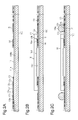
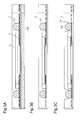
Figs. 2A to 2C ,3A to 3C ,4A, and 4B are schematic cross-sectional views illustrating the procedures for manufacturing the semiconductor device illustrated inFig. 1A ; -
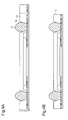
Fig. 5A is a schematic cross-sectional view of a second embodiment of the semiconductor device; -
Fig. 5B is a schematic plan view of the semiconductor device illustrated inFig. 5A ; -
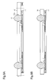
Figs. 6A to 6C ,7A to 7C ,8A, and 8B are the procedures for manufacturing the semiconductor device illustrated inFig. 5A ; -
Fig. 9A is a schematic cross-sectional view of another semiconductor device; -
Fig. 9B is a schematic plan view of the semiconductor device illustrated inFig. 9A ; and -
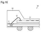
Fig. 10 is a schematic cross-sectional view of a comparative example of a semiconductor element. - One embodiment will now be described with reference to the accompanying drawings. Elements in the drawings are illustrated for simplicity and clarity and have not necessarily been drawn to scale. In the cross-sectional views, hatching of some elements is omitted.
- As illustrated in
Fig. 1A , a first embodiment of asemiconductor device 10 includes aninsulation layer 11 at the outermost layer (uppermost layer inFig. 1A ). - As illustrated in
Fig. 1B , theinsulation layer 11 is tetragonal and flat. The thickness of theinsulation layer 11 is, for example, 20 micrometers (µm). The material of theinsulation layer 11 is, for example, an organic resin, such as an epoxy resin or a polyimide resin. Also, an insulative resin including a reinforcement material may be used as the material of theinsulation layer 11. An insulative resin including a reinforcement material is formed, for example, by impregnating a thermosetting resin, such as epoxy or polyimide, in a reinforcement material, such as a woven cloth or a non-woven cloth using a fiber bundle, such as glass, aramid, or liquid crystal polymer (LCP). - As illustrated in
Fig. 1A , theinsulation layer 11 includes a first surface (lower surface 11a inFig. 1A ) and a second surface (upper surface 11b inFig. 1A ). Theupper surface 11b of theinsulation layer 11 forms the outermost surface (upper surface 10a inFig. 1A ) of thesemiconductor device 10. Awiring layer 12 is formed on thelower surface 11a of theinsulation layer 11. Thewiring layer 12 is formed on a peripheral region of theinsulation layer 11. The region where thewiring layer 12 is formed is set in correspondence with asemiconductor element 16. The material of thewiring layer 12 is, for example, copper (Cu). - The
wiring layer 12 includes a first surface (lower surface 12a inFig. 1A ) and a second surface (upper surface inFig. 1A ). The upper surface of thewiring layer 12 is covered by theinsulation layer 11. Thelower surface 12a of thewiring layer 12 is covered by a resistlayer 13. The material of the resistlayer 13 is, for example, an organic resin, such as an epoxy resin or a polyimide resin. The resistlayer 13 includesopenings lower surface 12a of thewiring layer 12. Theopening 13a exposes an inner portion of thelower surface 12a of thewiring layer 12 as aninternal connection pad 12b. Theopening 13b exposes an outer portion of thelower surface 12a of thewiring layer 12 as anexternal connection pad 12c. Surfaces of theconnection pads - A
bump 14 is formed on theinternal connection pad 12b. Thebump 14 is, for example, solder. Abump 15 is formed on theexternal connection pad 12c. Thebump 15 is, for example, solder. The material of a solder bump is, for example, an alloy of Sn and Cu, an alloy of Sn and silver (Ag), or an alloy of Sn, Ag, and Cu, or the like. Thebump 15 may be omitted. - The semiconductor element 16 (semiconductor chip) is connected to the
internal connection pads 12b. Thesemiconductor element 16 includes a first surface (upper surface 16a inFig. 1A ) and a second surface (lower surface 16g inFig. 1A ). Thesemiconductor element 16 is, for example, a sensor chip that detects the capacitance of an object (detection subject) proximate to theupper surface 16a of thesemiconductor element 16. An example of a detection subject is a human finger. The thickness of thesemiconductor element 16 is, for example, 200 µm. - As illustrated in
Fig. 1C , a plurality of theexternal connection pads 16b (electrode pads) are formed in the peripheral region of theupper surface 16a of thesemiconductor element 16. Theexternal connection pad 16b is, for example, tetragonal in a plan view. - A
detection region 16d, which serves as a circuit element region, is formed on theupper surface 16a of thesemiconductor element 16, for example, at an inner side of theexternal connection pad 16b. In the present embodiment, a circuit element (sensor element) used to detect an object is formed in thedetection region 16d. As illustrated inFig. 1C , thedetection region 16d is, for example, tetragonal in a plan view. Although formed on theupper surface 16a of thesemiconductor element 16, thedetection region 16d extends in the thicknesswise direction of thesemiconductor element 16 as illustrated by broken lines inFig. 1A . This is the same in the other accompanying drawings. - As illustrated in
Fig. 1A , abump 16e is formed on theexternal connection pad 16b (refer toFig. 1C ). Thebump 16e is, for example, gold. Thesemiconductor element 16 is electrically connected to thewiring layer 12 by thebumps - As described above, the
wiring layer 12 is formed in the region corresponding to thesemiconductor element 16 and covered by the resistlayer 13. Thewiring layer 12 is formed so as not to be overlapped with thedetection region 16d of theupper surface 16a of thesemiconductor element 16 in a plan view. Although thewiring layer 12 is not illustrated inFig. 1B , thewiring layer 12 is located in a region between outer edges of thedetection region 16d and theinsulation layer 11, more specifically, between an inner edge of the resistlayer 13 and the outer edge of theinsulation layer 11. Thus, theexternal connection pad 12c is located in a region where theexternal connection pad 12c is not overlapped with thesemiconductor element 16 in a plan view, that is, the outer side of thesemiconductor element 16. - As illustrated in
Fig. 1A , a gap formed by theupper surface 16a of thesemiconductor element 16, thelower surface 11a of theinsulation layer 11, and the resistlayer 13, is filled with anunderfill resin 17. Theunderfill resin 17 is, for example, an insulative resin such as an epoxy resin. Theunderfill resin 17 also substantially covers aside surface 16f of thesemiconductor element 16. - The
lower surface 16g of thesemiconductor element 16 is covered by aninsulation layer 18. Theinsulation layer 18 also covers theunderfill resin 17 and the resistlayer 13. That is, thesemiconductor element 16 is encapsulated by theinsulation layer 18. Theinsulation layer 18 is, for example, an insulative resin such as an epoxy resin. Theinsulation layer 18 is a mold resin that is formed by a transfer molding process, a compression molding process, an injection molding process, or the like. The thickness of theinsulation layer 18 is, for example, approximately 200 µm, at a location where theinsulation layer 18 covers thelower surface 16g of thesemiconductor element 16. - The
insulation layer 18 includes anopening 18a that exposes thebump 15. Anexternal connection terminal 19 is formed in theopening 18a. Theexternal connection terminal 19 is, for example, a solder ball. The material of a solder ball is, for example, an alloy of Sn and Cu, an alloy of Sn and Ag, an alloy of Sn, Ag, and Cu, or the like. The external connection terminal 19A includes a distal end (lower end inFig. 1A ) projecting beyond thelower surface 18b of theinsulation layer 18. Theexternal connection terminal 19 is used to connect a pad of a mount board (e.g., motherboard) on which thesemiconductor device 10 is mounted. Theexternal connection terminal 19 ensures a distance ("standoff") between the lower surface (here,lower surface 18b) of thesemiconductor device 10 and a mounting surface of the mount board which face toward each other. - The operation of the
semiconductor device 10 will now be described. - The
wiring layer 12 is not formed immediately above thedetection region 16d of thesemiconductor element 16. Thedetection region 16d is covered by theunderfill resin 17, which fills a gap between thelower surface 11a of theinsulation layer 11 and theupper surface 16a of thesemiconductor element 16. In other words, thedetection region 16d is covered by theunderfill resin 17 and theinsulation layer 11. The thickness of theunderfill resin 17 is determined by the thickness of thewiring layer 12 and the shapes of thebumps semiconductor element 16 to thewiring layer 12. In this manner, thedetection region 16d is not covered by an encapsulation resin, which is used in various types of molding processes. Thus, compared to when an encapsulation resin is used, theinsulation layer 11 and theunderfill resin 17, which cover thedetection region 16d, are thin, and thickness variations of theinsulation layer 11 and theunderfill resin 17 resulting from a manufacturing process are small. - This results in small variations resulting from the manufacturing process in the distance between the
upper surface 16a of thesemiconductor element 16, which includes thedetection region 16d, and theupper surface 11b of the insulation layer 11 (upper surface 10a of the semiconductor device 10) arranged as a contact surface of a detection subject. Thus, theinsulation layer 11 and theunderfill resin 17, which cover theupper surface 16a of thesemiconductor element 16, subtly affect a detecting operation of thesemiconductor element 16. - When the
semiconductor element 16 is a chip sensor that includes a sensor element, for example, a tactile sensor, in the circuit element region (detection region 16d), face-down mounting in which thedetection region 16d and the mount board face toward each other is not used. - Thus, as illustrated in
Fig. 10 , thesemiconductor element 16, which is a chip sensor, is face-up-mounted. In this case, in asemiconductor device 90, which is of a conventional type and includes thesemiconductor element 16, thesemiconductor element 16 is connected to awiring substrate 91 by abonding wire 92. Thebonding wire 92 is covered by, for example, a moldedresin 93. However, the moldedresin 93 may cause variations in the thickness depending on the conditions of the manufacturing process. The variations in the thickness of theresin 93 affect the operation (e.g., detection sensitivity, detection precision, or the like) of thesemiconductor element 16. - In contrast, the
semiconductor device 10 of the present embodiment has small variations in the distance between theupper surface 16a of thesemiconductor element 16, which includesdetection region 16d, and theupper surface 11b of the insulation layer 11 (upper surface 10a of the semiconductor device 10) during the manufacturing process. Thus, in thesemiconductor device 10, theinsulation layer 11 and theunderfill resin 17, which cover theupper surface 16a of thesemiconductor element 16 subtly affects the detecting operation of thesemiconductor element 16. - The procedures for manufacturing the
semiconductor device 10 will now be described with reference toFigs. 2A to 4B. Figs. 2A to 4B only have those reference characters that are used in the description of the steps. - The procedures for forming the structure illustrated in
Fig. 2A will now be described. As illustrated inFig. 2A , asupport plate 100 is prepared. Thesupport plate 100 is flat. The material of thesupport plate 100 is, for example, copper (Cu). The thickness of thesupport plate 100 is, for example, 0.1 to 0.2 mm. For example, thesupport plate 100 is large enough to simultaneously form a batch of thesemiconductor elements 16. - A film-like insulative resin is applied to an upper surface 100a of the
support plate 100 to form theinsulation layer 11. Thefirst surface 11a (upper surface inFig. 2A ) of theinsulation layer 11 undergoes, for example, an additive process, a semi-additive process, or the like, to form thewiring layer 12. Alternatively, theinsulation layer 11 and thewiring layer 12 may be formed by using a lamination film of theinsulation layer 11 and a metal layer. In such a case, the lamination film is applied so that theinsulation layer 11 faces the upper surface 100a of thesupport plate 100. The metal layer is etched to form thewiring layer 12. Thewiring layer 12 is covered by, for example, a photosensitive resin film, and the resin film is patterned by a photolithography. This forms the resistlayer 13 that includes theopenings first surface 12a (upper surface inFig. 2A ) of thewiring layer 12 through theopenings bumps - The procedures for forming the structure illustrated in
Fig. 2B will now be described. Thesemiconductor element 16 is prepared. Thefirst surface 16a (lower surface inFig. 2B ) of thesemiconductor element 16 includes thebump 16e. - A resin film is applied to cover the
internal connection pads 12b of thewiring layer 12. The resin film is partially cured. In a state in which thefirst surface 16a of thesemiconductor element 16 faces an upper surface of the resin film, thesemiconductor element 16 is pressed to the resin film by applying pressure in a high temperature (thermal pressure bonding). This connects thebump 16e of thesemiconductor element 16 to thebump 14 of thefirst surface 12a (upper surface inFig. 2B ) of thewiring layer 12. The force produced by a distal end of thebump 16e contacting thefirst surface 12a of thewiring layer 12 is used to press thesemiconductor element 16. This accurately sets the distance between thefirst surface 16a of thesemiconductor element 16 and thefirst surface 12a of thewiring layer 12. The resin film, which has been softened by the thermal pressure bonding, is hardened to form theunderfill resin 17. Then, theunderfill resin 17 is completely hardened by curing (thermosetting process). - As illustrated in
Fig. 2C , asolder bump 19a is formed on theexternal connection pad 12c. Thesolder bump 19a is obtained by, for example, mounting a spherical solder ball on theexternal connection pad 12c and performing a reflow process on the solder ball. - As illustrated in
Fig. 3A , an upper surface of the structure illustrated inFig. 2C is entirely encapsulated (molded) by a resin. For example, the structure ofFig. 2C undergoes a transfer molding process, a compression molding process, an injection molding process, or the like. This forms theinsulation layer 18 that covers thesemiconductor element 16, theunderfill resin 17, and thesolder bump 19a. - As illustrated in
Fig. 3B , thesupport plate 100 is removed. For example, when thesupport plate 100 is formed from copper, thesupport plate 100 is removed by etching. - As illustrated in
Fig. 3C , theopening 18a is formed in theinsulation layer 18 to expose thesolder bump 19a. For example, a laser processing device is used to form theopening 18a. - As illustrated in
Fig. 4A , theexternal connection terminal 19 is formed. Theexternal connection terminal 19 is obtained by applying a conductive material, such as a solder paste or a solder ball, to thesolder bump 19a illustrated inFig. 3C and performing a reflow process on the conductive material. - As illustrated in
Fig. 4B , the structure ofFig. 4A is cut along predetermined positions (broken lines illustrated inFig. 4B ) to obtain an individual piece of thesemiconductor device 10. For the sake of the illustration of manufacturing procedures, the structure ofFig. 1A is reversed upside-down inFigs. 2A to 4B . - The first embodiment has the advantages described below.
- (1-1) The
semiconductor device 10 includes theinsulation layer 11 at the uppermost position. Thewiring layer 12 is formed on thelower surface 11a (first surface) of theinsulation layer 11. Thelower surface 12a (first surface) of thewiring layer 12 is covered by the resistlayer 13. The resistlayer 13 includes theopenings lower surface 12a of thewiring layer 12. Theopening 13a exposes the inner portion of thelower surface 12a of thewiring layer 12 as theinternal connection pad 12b. Theopening 13b exposes the outer portion of thelower surface 12a of thewiring layer 12 as theexternal connection pad 12c. Theinternal connection pads 12b are connected to thesemiconductor element 16. - The
detection region 16d is formed on theupper surface 16a (first surface) of thesemiconductor element 16. Theupper surface 16a of thesemiconductor element 16 is covered by theinsulation layer 11 and theunderfill resin 17. Thesemiconductor element 16 is electrically connected to thewiring layer 12 formed on thelower surface 11a of theinsulation layer 11 by bonding thebump 16e to thebump 14. Thewiring layer 12 includes theexternal connection pads 12c at the outer side of theinternal connection pads 12b, which are connected to thesemiconductor element 16. Thesemiconductor device 10 is mounted on theexternal connection pads 12c. - This results in small variations resulting from the manufacturing process in the distance between the
upper surface 16a of thesemiconductor element 16, which includes thedetection region 16d, and theupper surface 11b (second surface)of theinsulation layer 11 arranged as the contact surface of a detection subject. Thus, theinsulation layer 11 and theunderfill resin 17, which cover theupper surface 16a of thesemiconductor element 16, subtly affect the detecting operation of thesemiconductor element 16. - (1-2) The
insulation layer 11 is formed on the upper surface 100a of thesupport plate 100. Thewiring layer 12 is formed on thefirst surface 11a of theinsulation layer 11. Then, thesemiconductor element 16 is connected to theinternal connection pads 12b of thewiring layer 12. Thesemiconductor element 16 is covered by theinsulation layer 18. Thesupport plate 100 is removed. Theopening 18a is formed in theinsulation layer 18. Theexternal connection terminal 19 is formed in theopening 18a. This allows for easy formation of thesemiconductor device 10 in which thethin insulation layer 11 and thethin underfill resin 17 cover thefirst surface 16a of thesemiconductor element 16, which includes the circuit element region (detection region 16d). - A second embodiment will now be described. In the second embodiment, the same reference characters are given to those components that are the same as the corresponding components of the first embodiment. The description of such components will be omitted partially or entirely.
- As illustrated in
Fig. 5A , asemiconductor device 30 includes theinsulation layer 11 at the uppermost position. Thewiring layer 12 is formed on thelower surface 11a (first surface) of theinsulation layer 11. Thelower surface 12a (first surface) of thewiring layer 12 is covered by a first resistlayer 31. The material of the first resistlayer 31 is, for example, an organic resin, such as an epoxy resin or a polyimide resin. A second resistlayer 32 is formed on alower surface 31a (first surface) of the first resistlayer 31. The second resistlayer 32 covers a peripheral portion of thelower surface 31a of the first resistlayer 31. The first resistlayer 31 includes anopening 33. Theopening 33 exposes an inner portion of thelower surface 12a of thewiring layer 12 as theinternal connection pad 12b. Anopening 34 is formed in the first and second resistlayers opening 34 exposes an outer portion of thelower surface 12a of thewiring layer 12 as theexternal connection pad 12c. In the same manner as the first resistlayer 31, the material of the second resistlayer 32 is, for example, an organic resin, such as an epoxy resin or a polyimide resin. The first and second resistlayers - The outer edge of the
insulation layer 11 and the outer edges of the first and second resistlayers insulation layer 18. For example, as illustrated inFig. 5B , theinsulation layer 11 has a tetragonal shape that is smaller than theinsulation layer 18, and corners of theinsulation layer 11 are rounded in a plan view. Thus, thesemiconductor device 30 includes astep 41 at the outer edge. Thestep 41 allows for easy coupling (e.g., alignment) of thesemiconductor device 30 to an electronic device. Also, thestep 41 is arranged to determine the attachment position of thesemiconductor device 30 in an electronic device, for example, the position of anupper surface 30a of thesemiconductor device 30 relative to a surface of the electronic device. - The procedures for manufacturing the
semiconductor device 30 will now be described. - The procedures for forming the structure illustrated in
Fig. 6A will now be described. As illustrated inFig. 6A , asupport plate 110 is prepared. Thesupport plate 110 includes aflat support portion 111 and aprojection portion 112 projecting upward from afirst surface 111a (upper surface inFig. 6A ) of thesupport portion 111. Theprojection portion 112 has the shape of a lattice that corresponds to the position of thestep 41 of thesemiconductor device 30 illustrated inFig. 5B . A film-like insulative resin is applied to thefirst surface 111 a of thesupport portion 111 to form theinsulation layer 11. Thefirst surface 111 a of thesupport portion 111 undergoes, for example, an additive process, a semi-additive process, or the like, to form thewiring layer 12. In the same manner asFig. 2A , theinsulation layer 11 and thewiring layer 12 may be formed by applying a lamination film of theinsulation layer 11 and a metal layer to thesupport portion 111 and etching the metal layer. - The
wiring layer 12 is covered by, for example, a photosensitive resin film, and the resin film is patterned by a photolithography. This forms the first resistlayer 31 that includes theopening 33. In the same manner, the first resistlayer 31 is covered by, for example, a photosensitive resin film, and the resin film is patterned by a photolithography. This forms the second resistlayer 32 that includes theopening 34. A conductive material (e.g., solder paste) is applied to thefirst surface 12a of thewiring layer 12 through theopenings bumps - The procedures for forming the structure illustrated in
Fig. 6B will now be described. A resin film is applied to cover theinternal connection pads 12b of thewiring layer 12. The resin film is partially cured. In a state in which thefirst surface 16a of thesemiconductor element 16 faces an upper surface of the resin film, thesemiconductor element 16 is pressed to the resin film by applying pressure in a high temperature (thermal pressure bonding). This connects thebump 16e of thefirst surface 12a of thewiring layer 12 to thebump 14 of thesemiconductor element 16. The resin film, which has been softened by the thermal pressure bonding, is hardened to form theunderfill resin 17. Then, theunderfill resin 17 is completely hardened by curing (thermosetting process). - As illustrated in
Fig. 6C , thesolder bump 19a is formed on theexternal connection pad 12c. Thesolder bump 19a is obtained by, for example, mounting a spherical solder ball on theexternal connection pad 12c and performing a reflow process on the solder ball. - As illustrated in
Fig. 7A , an upper surface of the structure illustrated inFig. 6C is entirely encapsulated (molded) by a resin. For example, the structure ofFig. 6C undergoes a transfer molding process, a compression molding process, an injection molding process, or the like. This forms theinsulation layer 18 that covers thesemiconductor element 16, theunderfill resin 17, and thesolder bump 19a. - As illustrated in
Fig. 7B , thesupport plate 110 is removed. For example, when thesupport plate 110 is formed from copper, thesupport plate 110 is removed by etching. A groove portion 43 (recessed portion) having the shape of a lattice is formed by removing thesupport plate 110. - As illustrated in
Fig. 7C , theopening 18a is formed in theinsulation layer 18 to expose thesolder bump 19a. For example, a laser processing device is used to form theopening 18a. - As illustrated in
Fig. 8A , theexternal connection terminal 19 is formed. Theexternal connection terminal 19 is obtained by applying a conductive material, such as a solder paste or a solder ball, to thesolder bump 19a illustrated inFig. 7C and performing a reflow process on the conductive material. - As illustrated in
Fig. 8B , the structure ofFig. 8A is cut along predetermined positions (broken lines illustrated inFig. 8B ) of thegroove portion 43 to obtain an individual piece of thesemiconductor device 30. Thesemiconductor device 30 includes thestep 41. For the sake of the illustration of manufacturing steps, the structure ofFig. 5A is reversed upside-down inFigs. 6A to 8B . - The second embodiment has the following advantages in addition to the advantages of the first embodiment.
- (2-1) The
semiconductor device 30 includes theinsulation layer 11 at the uppermost position. Thewiring layer 12 is formed on thelower surface 11a (first surface) of theinsulation layer 11. Thelower surface 12a (first surface) of thewiring layer 12 is covered by the first resistlayer 31. The peripheral portion of the first resistlayer 31 is covered by the second resistlayer 32. The outer edge of theinsulation layer 11 and the outer edges of the first and second resistlayers insulation layer 18. Theinsulation layer 11 has the tetragonal shape that is smaller than theinsulation layer 18, and the edges are chamfered to have an arcuate shape in a plan view. Thus, thesemiconductor device 30 includes thestep 41 at the outer edge. This provides thesemiconductor device 30 including thestep 41 that corresponds to the thickness of theinsulation layer 11 and the thicknesses of the first and second resistlayers - (2-2) The
support plate 110 includes theflat support portion 111 and theprojection portion 112, which has the shape of a lattice and projects from thesupport portion 111. Theinsulation layer 11 is formed on thesupport portion 111. Thewiring layer 12 is formed on thefirst surface 11a of theinsulation layer 11. Thesemiconductor element 16 is connected to theinternal connection pads 12b of thewiring layer 12. Thesemiconductor element 16 is covered by theinsulation layer 18. Thesupport plate 110 is removed. The removal of thesupport portion 111 forms thegroove portion 43 that corresponds to theprojection portion 112. Then, theopening 18a is formed in theinsulation layer 18. Theexternal connection terminal 19 is formed in theopening 18a. This allows for easy formation of thesemiconductor device 30 in which thethin insulation layer 11 and thethin underfill resin 17 cover thefirst surface 16a of thesemiconductor element 16, which includes the circuit element region (detection region 16d). Also, thesemiconductor device 30 includes thestep 41. This allows for easy coupling of thesemiconductor device 30 to an electronic device. - It should be apparent to those skilled in the art that the present invention may be embodied in many other specific forms without departing from the scope of the invention. Particularly, it should be understood that the present invention may be embodied in the following forms.
- In the second embodiment, the shape of the
step 41 of thesemiconductor device 30 may be modified. - For example, as illustrated in
Fig. 9B , astep 41 may be formed only on corners of asemiconductor device 50. In the same manner as thesemiconductor device 10 of the first embodiment, as illustrated inFig. 9A , thesemiconductor device 50 includes the single resistlayer 13 formed on thefirst surface 11a of theinsulation layer 11. Instead, thesemiconductor device 50 may include the first and second resistlayers - The shape of the
step 41 may be modified. For example, thestep 41 may be formed by cutting away corners of theinsulation layer 11 in a straight line. For example, in the second embodiment, thestep 41 may be formed by forming theoctagonal insulation layer 11 in a plan view. - In the second embodiment, the
step 41 is formed by theinsulation layer 11 and the first and second resistlayers insulation layer 18. For example, the upper surface of theinsulation layer 18 may be covered by another resist layer. Alternatively, the height of theprojection portion 112 illustrated inFig. 6A may be changed during the process for manufacturing thesemiconductor device 30 to change the film thicknesses of the first and second resistlayers step 41 formed by theprojection portion 112. - The shape of the
detection region 16d illustrated inFig. 1C is one example and thus may be modified, for example, to be circular in a plan view. Alternatively, a plurality of detection regions may be formed on theupper surface 16a of thesemiconductor element 16. - In the above embodiments, the
support plates support plates copper support plates insulation layer 11, for example, with an adhesive agent. Thesupport plates - In
Fig. 1C , theexternal connection pads 16b are arranged in a tetragonal layout along the periphery of thesemiconductor element 16. However, theexternal connection pads 16b are not limited to such a layout. For example, theexternal connection pads 16b may be located along two opposing sides of thesemiconductor element 16. Alternatively, theexternal connection pads 16b may be arranged in a plurality of rows (e.g., two rows) along the side of thesemiconductor element 16. - The
step 41 may be formed by mechanically processing theinsulation layer 11, the resist layer, and the like using a routing machine, or the like. - In the second embodiment, a plurality of second resist layers may be stacked. The
step 41 may be formed by partially or entirely using the second resist layers. - For example, the
bumps Fig. 1A may be omitted from the above embodiments. - In the above embodiments, the
external connection terminal 19 illustrated inFig. 1A does not have to be projected beyond thelower surface 18b of theinsulation layer 18 in accordance with the mountedsemiconductor devices Fig. 4A (step to form theexternal connection terminal 19 applying a conductive material to thebump 19a) may be omitted. - In the above embodiments, the shape of the resist
layers Figs. 1A and 1B , the resistlayer 13 covers thelower surface 11a (first surface) of theinsulation layer 11 at the outer side of thedetection region 16d of thesemiconductor element 16. Instead, the resistlayer 13 may be formed to be partially overlapped with thedetection region 16d or to entirely cover thelower surface 11a of theinsulation layer 11 in a plan view. - The present examples and embodiments are to be considered as illustrative and not restrictive, and the invention is not to be limited to the details given herein, but may be modified within the scope and equivalence of the appended claims.
Claims (11)
- A semiconductor device (10 or 30) comprising:a first insulation layer (11);a wiring layer (12) formed on a first surface (11a) of the first insulation layer (11), the wiring layer (12) including
an external connection pad (12c) located at a position corresponding to a periphery of the first insulation layer (11), and
an internal connection pad (12b) located at an inner side of the external connection pad (12c);a semiconductor element (16) located facing the first surface (11a) of the first insulation layer (11), the semiconductor element (16) including
an electrode pad (16b) formed on a first surface (16a) of the semiconductor element (16) that faces the first surface (11a) of the first insulation layer (11) and located at a position corresponding to the internal connection pad (12b) of the wiring layer (12),
a bump (16e) formed on the electrode pad (16b) and connected to the internal connection pad (12b), and
a circuit element region (16d) defined in the first surface (16a) of the semiconductor element (16) at an inner side of the electrode pad (16b);a second insulation layer (17) that fills a gap between the first surface (16a) of the semiconductor element (16) and the first surface (11a) of the first insulation layer (11);a third insulation layer (18) that covers a second surface (16g) of the semiconductor element (16) and the second insulation layer (17), wherein the third insulation layer (18) includes an opening (18a) at a position corresponding to the external connection pad (12c), and the second surface (16g) of the semiconductor element (16) is located at a side opposite to the first surface (16a) of the semiconductor element (16); andan external connection terminal (19) connected to the external connection pad (12c). - The semiconductor device (10 or 30) according to claim 1, wherein
the external connection pad (12c) and the internal connection pad (12b) are formed on a first surface (12a) of the wiring layer (12), and
the semiconductor device (10 or 30) further comprises a resist layer (13 or 31,32) that covers the first surface (12a) of the wiring layer (12), the resist layer (13 or 31,32) including
a first opening (13a or 33) that exposes an inner portion of the first surface (12a) of the wiring layer (12) as the internal connection pad (12b), and
a second opening (13b or 34) that exposes an outer portion of the first surface (12a) of the wiring layer (12) as the external connection pad (12c). - The semiconductor device (30) according to claim 2, wherein
the resist layer (31,32) includes
a first resist layer (31) that covers the first surface (12a) of the wiring layer (12), and
a second resist layer (32) that covers a peripheral portion of the first resist layer (31),
the first opening (33) extends through the first resist layer (31), and
the second opening (34) extends through the first and second resist layers (31,32). - The semiconductor device (10 or 30) according to any one of claims 1 to 3, wherein the semiconductor element (16) is a sensor chip and includes sensor elements formed in the circuit element region (16d).
- The semiconductor device (10 or 30) according to any one of claims 1 to 4, wherein the wiring layer (12) is located in a region where the wiring layer (12) is not overlapped with the circuit element region (16d) of the semiconductor element (16) in a plan view.
- The semiconductor device (10 or 30) according to any one of claims 1 to 5, wherein the external connection pad (19) is located at an outer side of the semiconductor element (16) in a plan view.
- The semiconductor device (10 or 30) according to any one of claims 1 to 6, wherein the second insulation layer (17) extends to a location between the external connection pad (12c) and the internal connection pad (12b) and covers a side surface (16f) of the semiconductor element (16).
- The semiconductor device (10 or 30) according to any one of claims 1 to 7, wherein
the first insulation layer (11) includes a second surface (11b) that is located at a side opposite to the first surface (11a) of the first insulation layer (11), and
the second surface (11b) of the first insulation layer (11) forms an outermost surface (10a) of the semiconductor device (10 or 30). - A method for manufacturing a semiconductor device (10 or 30), the method comprising:forming an insulation layer (11) on an upper surface (100a) of a support plate (100);forming a wiring layer (12) on an upper surface (11a) of the insulation layer (11);connecting a semiconductor element (16) to an internal connection pad (12b) of the wiring layer (12);forming a resin layer (18) that covers the semiconductor element (16);removing the support plate (100);forming an opening (18a) in the resin layer (18); andforming an external connection terminal (19) in the opening (18a) so that the external connection terminal (19) is connected to an external connection pad (12c) of the wiring layer (12).
- The method according to claim 9, further comprising connecting a first connection terminal (19a) to the external connection pad (12c) of the wiring layer (12) before the forming a resin layer (18), wherein
the forming a resin layer (18) includes covering the semiconductor element (16) and the first connection terminal (19a) by the resin layer (18),
the forming an opening (18a) in the resin layer (18) includes exposing the first connection terminal (19a) in the opening (18a), and
the forming an external connection terminal (19) includes applying a conductive material to the first connection terminal (19a) so as to form the external connection terminal (19) that projects beyond a surface of the resin layer (18). - The method according to claim 9 or 10, further comprising forming a resist layer (31,32) covering the wiring layer (12), wherein
the support plate (110) includes a projection portion (112) for forming a recessed portion (43) extending through the insulation layer (11) and the resist layer (31,32),
the recessed portion (43) exposes an edge portion of the insulation layer (11) and an edge portion of the resist layer (31,32) when the support plate (110) is removed,
the method further comprises cutting the resin layer (18) at the recessed portion (43) to form a step (41) at an edge portion of the semiconductor device (30), the step (41) being formed by the edge portion of the insulation layer (11), the edge portion of the resist layer (31,32), and an edge portion of the resin layer (18).
Applications Claiming Priority (1)
| Application Number | Priority Date | Filing Date | Title |
|---|---|---|---|
| JP2014003530A JP6335513B2 (en) | 2014-01-10 | 2014-01-10 | Semiconductor device and method for manufacturing semiconductor device |
Publications (2)
| Publication Number | Publication Date |
|---|---|
| EP2897163A1 true EP2897163A1 (en) | 2015-07-22 |
| EP2897163B1 EP2897163B1 (en) | 2020-12-09 |
Family
ID=52232094
Family Applications (1)
| Application Number | Title | Priority Date | Filing Date |
|---|---|---|---|
| EP15150271.3A Active EP2897163B1 (en) | 2014-01-10 | 2015-01-07 | Semiconductor device and method of manufacturing a semiconductor device |
Country Status (3)
| Country | Link |
|---|---|
| US (1) | US9397061B2 (en) |
| EP (1) | EP2897163B1 (en) |
| JP (1) | JP6335513B2 (en) |
Families Citing this family (7)
| Publication number | Priority date | Publication date | Assignee | Title |
|---|---|---|---|---|
| JP2015195263A (en) * | 2014-03-31 | 2015-11-05 | マイクロン テクノロジー, インク. | Semiconductor device and manufacturing method or the same |
| TWI566305B (en) * | 2014-10-29 | 2017-01-11 | 巨擘科技股份有限公司 | Method for manufacturing three-dimensional integrated circuit |
| US20180053753A1 (en) * | 2016-08-16 | 2018-02-22 | Freescale Semiconductor, Inc. | Stackable molded packages and methods of manufacture thereof |
| US10199356B2 (en) | 2017-02-24 | 2019-02-05 | Micron Technology, Inc. | Semiconductor device assembles with electrically functional heat transfer structures |
| US10096576B1 (en) | 2017-06-13 | 2018-10-09 | Micron Technology, Inc. | Semiconductor device assemblies with annular interposers |
| US10090282B1 (en) | 2017-06-13 | 2018-10-02 | Micron Technology, Inc. | Semiconductor device assemblies with lids including circuit elements |
| KR102594282B1 (en) * | 2021-10-13 | 2023-10-26 | 주식회사 에스에프에이반도체 | Manufacturing method of CIS semiconductor package |
Citations (7)
| Publication number | Priority date | Publication date | Assignee | Title |
|---|---|---|---|---|
| JP2001223297A (en) | 1999-11-30 | 2001-08-17 | Fujitsu Ltd | Semiconductor device, method of manufacturing semiconductor device, and method of stacking semiconductor device |
| JP2003007910A (en) | 2001-06-19 | 2003-01-10 | Matsushita Electric Ind Co Ltd | Semiconductor device |
| US20100097080A1 (en) * | 2008-10-22 | 2010-04-22 | Fujitsu Limited | Contact sensor unit, electronic device, and method for producing a contact sensor unit |
| US20100171207A1 (en) * | 2009-01-07 | 2010-07-08 | Chi-Chih Shen | Stackable semiconductor device packages |
| US20120112764A1 (en) * | 2010-11-05 | 2012-05-10 | AuthenTec, Inc., State of Incorporation: Delaware | Method of making a finger sensor package and associated devices |
| US20120299183A1 (en) * | 2010-02-17 | 2012-11-29 | Canon Kabushiki Kaisha | Semiconductor device and stacked-type semiconductor device |
| US20130221452A1 (en) * | 2011-09-15 | 2013-08-29 | Stats Chippac, Ltd. | Semiconductor Device and Method of Forming Semiconductor Die with Active Region Responsive to External Stimulus |
Family Cites Families (9)
| Publication number | Priority date | Publication date | Assignee | Title |
|---|---|---|---|---|
| US6458622B1 (en) * | 1999-07-06 | 2002-10-01 | Motorola, Inc. | Stress compensation composition and semiconductor component formed using the stress compensation composition |
| JP3683179B2 (en) * | 2000-12-26 | 2005-08-17 | 松下電器産業株式会社 | Semiconductor device and manufacturing method thereof |
| JP2003282609A (en) * | 2002-03-27 | 2003-10-03 | Fujitsu Ltd | Fingerprint recognition semiconductor device and manufacturing method thereof |
| JP4204989B2 (en) * | 2004-01-30 | 2009-01-07 | 新光電気工業株式会社 | Semiconductor device and manufacturing method thereof |
| JP2008205317A (en) * | 2007-02-21 | 2008-09-04 | Nec Electronics Corp | Solid-state imaging device, manufacturing method thereof, and electronic apparatus using the same |
| US8592992B2 (en) * | 2011-12-14 | 2013-11-26 | Stats Chippac, Ltd. | Semiconductor device and method of forming vertical interconnect structure with conductive micro via array for 3-D Fo-WLCSP |
| US8717775B1 (en) | 2010-08-02 | 2014-05-06 | Amkor Technology, Inc. | Fingerprint sensor package and method |
| JP5992676B2 (en) * | 2011-11-25 | 2016-09-14 | 京セラ株式会社 | Wiring board manufacturing method |
| US9543373B2 (en) * | 2013-10-23 | 2017-01-10 | Taiwan Semiconductor Manufacturing Company, Ltd. | Semiconductor structure and manufacturing method thereof |
-
2014
- 2014-01-10 JP JP2014003530A patent/JP6335513B2/en active Active
-
2015
- 2015-01-07 US US14/591,209 patent/US9397061B2/en active Active
- 2015-01-07 EP EP15150271.3A patent/EP2897163B1/en active Active
Patent Citations (7)
| Publication number | Priority date | Publication date | Assignee | Title |
|---|---|---|---|---|
| JP2001223297A (en) | 1999-11-30 | 2001-08-17 | Fujitsu Ltd | Semiconductor device, method of manufacturing semiconductor device, and method of stacking semiconductor device |
| JP2003007910A (en) | 2001-06-19 | 2003-01-10 | Matsushita Electric Ind Co Ltd | Semiconductor device |
| US20100097080A1 (en) * | 2008-10-22 | 2010-04-22 | Fujitsu Limited | Contact sensor unit, electronic device, and method for producing a contact sensor unit |
| US20100171207A1 (en) * | 2009-01-07 | 2010-07-08 | Chi-Chih Shen | Stackable semiconductor device packages |
| US20120299183A1 (en) * | 2010-02-17 | 2012-11-29 | Canon Kabushiki Kaisha | Semiconductor device and stacked-type semiconductor device |
| US20120112764A1 (en) * | 2010-11-05 | 2012-05-10 | AuthenTec, Inc., State of Incorporation: Delaware | Method of making a finger sensor package and associated devices |
| US20130221452A1 (en) * | 2011-09-15 | 2013-08-29 | Stats Chippac, Ltd. | Semiconductor Device and Method of Forming Semiconductor Die with Active Region Responsive to External Stimulus |
Also Published As
| Publication number | Publication date |
|---|---|
| JP2015133388A (en) | 2015-07-23 |
| US20150200175A1 (en) | 2015-07-16 |
| EP2897163B1 (en) | 2020-12-09 |
| US9397061B2 (en) | 2016-07-19 |
| JP6335513B2 (en) | 2018-05-30 |
Similar Documents
| Publication | Publication Date | Title |
|---|---|---|
| EP2897163B1 (en) | Semiconductor device and method of manufacturing a semiconductor device | |
| EP3007102B1 (en) | Semiconductor device and method for manufacturing semiconductor device | |
| CN110739275B (en) | Fingerprint sensor and method of manufacturing the same | |
| US8344492B2 (en) | Semiconductor device and method of manufacturing the same, and electronic apparatus | |
| US8835228B2 (en) | Substrate-less stackable package with wire-bond interconnect | |
| KR102367404B1 (en) | Method of manufacturing semiconductor package | |
| CN104685622A (en) | BVA interposer | |
| KR20140126598A (en) | semiconductor package and method for manufacturing of the same | |
| US20100213605A1 (en) | Semiconductor device and method of manufacturing semiconductor device | |
| CN108695269B (en) | Semiconductor device package and method of manufacturing the same | |
| US9980371B2 (en) | Printed wiring board | |
| US11756896B2 (en) | Semiconductor package structure including shielding layer contacting conductive contact | |
| JP2003338587A (en) | Semiconductor device and manufacturing method thereof | |
| CN101154641A (en) | Semiconductor device and manufacturing method thereof | |
| CN101308802A (en) | Sensing type semiconductor device and manufacturing method thereof | |
| US7964493B2 (en) | Method of manufacturing semiconductor device | |
| KR20090029646A (en) | Manufacturing Method of Semiconductor Device | |
| US8674503B2 (en) | Circuit board, fabricating method thereof and package structure | |
| TWI630665B (en) | Method of making chip package structure | |
| JP2002231765A (en) | Semiconductor device | |
| TW201830592A (en) | Package structure and its manufacturing method | |
| US11862544B2 (en) | Electronic assembly | |
| KR20150033912A (en) | Ultra thin type printed circuit board and semiconductor package including the same and method of manufacturing the semiconductor package | |
| KR20140027645A (en) | A method for manufacturing a chip embedded substrate |
Legal Events
| Date | Code | Title | Description |
|---|---|---|---|
| PUAI | Public reference made under article 153(3) epc to a published international application that has entered the european phase |
Free format text: ORIGINAL CODE: 0009012 |
|
| 17P | Request for examination filed |
Effective date: 20150107 |
|
| AK | Designated contracting states |
Kind code of ref document: A1 Designated state(s): AL AT BE BG CH CY CZ DE DK EE ES FI FR GB GR HR HU IE IS IT LI LT LU LV MC MK MT NL NO PL PT RO RS SE SI SK SM TR |
|
| AX | Request for extension of the european patent |
Extension state: BA ME |
|
| 17P | Request for examination filed |
Effective date: 20160126 |
|
| RBV | Designated contracting states (corrected) |
Designated state(s): AL AT BE BG CH CY CZ DE DK EE ES FI FR GB GR HR HU IE IS IT LI LT LU LV MC MK MT NL NO PL PT RO RS SE SI SK SM TR |
|
| STAA | Information on the status of an ep patent application or granted ep patent |
Free format text: STATUS: EXAMINATION IS IN PROGRESS |
|
| 17Q | First examination report despatched |
Effective date: 20170921 |
|
| GRAP | Despatch of communication of intention to grant a patent |
Free format text: ORIGINAL CODE: EPIDOSNIGR1 |
|
| STAA | Information on the status of an ep patent application or granted ep patent |
Free format text: STATUS: GRANT OF PATENT IS INTENDED |
|
| RIC1 | Information provided on ipc code assigned before grant |
Ipc: H01L 23/31 20060101AFI20190919BHEP Ipc: H01L 21/56 20060101ALI20190919BHEP |
|
| INTG | Intention to grant announced |
Effective date: 20191022 |
|
| GRAS | Grant fee paid |
Free format text: ORIGINAL CODE: EPIDOSNIGR3 |
|
| GRAJ | Information related to disapproval of communication of intention to grant by the applicant or resumption of examination proceedings by the epo deleted |
Free format text: ORIGINAL CODE: EPIDOSDIGR1 |
|
| GRAL | Information related to payment of fee for publishing/printing deleted |
Free format text: ORIGINAL CODE: EPIDOSDIGR3 |
|
| STAA | Information on the status of an ep patent application or granted ep patent |
Free format text: STATUS: EXAMINATION IS IN PROGRESS |
|
| INTC | Intention to grant announced (deleted) | ||
| GRAP | Despatch of communication of intention to grant a patent |
Free format text: ORIGINAL CODE: EPIDOSNIGR1 |
|
| STAA | Information on the status of an ep patent application or granted ep patent |
Free format text: STATUS: GRANT OF PATENT IS INTENDED |
|
| INTG | Intention to grant announced |
Effective date: 20200826 |
|
| GRAS | Grant fee paid |
Free format text: ORIGINAL CODE: EPIDOSNIGR3 |
|
| GRAA | (expected) grant |
Free format text: ORIGINAL CODE: 0009210 |
|
| STAA | Information on the status of an ep patent application or granted ep patent |
Free format text: STATUS: THE PATENT HAS BEEN GRANTED |
|
| AK | Designated contracting states |
Kind code of ref document: B1 Designated state(s): AL AT BE BG CH CY CZ DE DK EE ES FI FR GB GR HR HU IE IS IT LI LT LU LV MC MK MT NL NO PL PT RO RS SE SI SK SM TR |
|
| REG | Reference to a national code |
Ref country code: GB Ref legal event code: FG4D |
|
| REG | Reference to a national code |
Ref country code: AT Ref legal event code: REF Ref document number: 1344266 Country of ref document: AT Kind code of ref document: T Effective date: 20201215 Ref country code: CH Ref legal event code: EP |
|
| REG | Reference to a national code |
Ref country code: DE Ref legal event code: R096 Ref document number: 602015063131 Country of ref document: DE |
|
| REG | Reference to a national code |
Ref country code: IE Ref legal event code: FG4D |
|
| PG25 | Lapsed in a contracting state [announced via postgrant information from national office to epo] |
Ref country code: GR Free format text: LAPSE BECAUSE OF FAILURE TO SUBMIT A TRANSLATION OF THE DESCRIPTION OR TO PAY THE FEE WITHIN THE PRESCRIBED TIME-LIMIT Effective date: 20210310 Ref country code: FI Free format text: LAPSE BECAUSE OF FAILURE TO SUBMIT A TRANSLATION OF THE DESCRIPTION OR TO PAY THE FEE WITHIN THE PRESCRIBED TIME-LIMIT Effective date: 20201209 Ref country code: RS Free format text: LAPSE BECAUSE OF FAILURE TO SUBMIT A TRANSLATION OF THE DESCRIPTION OR TO PAY THE FEE WITHIN THE PRESCRIBED TIME-LIMIT Effective date: 20201209 Ref country code: NO Free format text: LAPSE BECAUSE OF FAILURE TO SUBMIT A TRANSLATION OF THE DESCRIPTION OR TO PAY THE FEE WITHIN THE PRESCRIBED TIME-LIMIT Effective date: 20210309 |
|
| REG | Reference to a national code |
Ref country code: AT Ref legal event code: MK05 Ref document number: 1344266 Country of ref document: AT Kind code of ref document: T Effective date: 20201209 |
|
| PG25 | Lapsed in a contracting state [announced via postgrant information from national office to epo] |
Ref country code: BG Free format text: LAPSE BECAUSE OF FAILURE TO SUBMIT A TRANSLATION OF THE DESCRIPTION OR TO PAY THE FEE WITHIN THE PRESCRIBED TIME-LIMIT Effective date: 20210309 Ref country code: SE Free format text: LAPSE BECAUSE OF FAILURE TO SUBMIT A TRANSLATION OF THE DESCRIPTION OR TO PAY THE FEE WITHIN THE PRESCRIBED TIME-LIMIT Effective date: 20201209 Ref country code: LV Free format text: LAPSE BECAUSE OF FAILURE TO SUBMIT A TRANSLATION OF THE DESCRIPTION OR TO PAY THE FEE WITHIN THE PRESCRIBED TIME-LIMIT Effective date: 20201209 |
|
| REG | Reference to a national code |
Ref country code: NL Ref legal event code: MP Effective date: 20201209 |
|
| PG25 | Lapsed in a contracting state [announced via postgrant information from national office to epo] |
Ref country code: NL Free format text: LAPSE BECAUSE OF FAILURE TO SUBMIT A TRANSLATION OF THE DESCRIPTION OR TO PAY THE FEE WITHIN THE PRESCRIBED TIME-LIMIT Effective date: 20201209 Ref country code: HR Free format text: LAPSE BECAUSE OF FAILURE TO SUBMIT A TRANSLATION OF THE DESCRIPTION OR TO PAY THE FEE WITHIN THE PRESCRIBED TIME-LIMIT Effective date: 20201209 |
|
| REG | Reference to a national code |
Ref country code: LT Ref legal event code: MG9D |
|
| PG25 | Lapsed in a contracting state [announced via postgrant information from national office to epo] |
Ref country code: LT Free format text: LAPSE BECAUSE OF FAILURE TO SUBMIT A TRANSLATION OF THE DESCRIPTION OR TO PAY THE FEE WITHIN THE PRESCRIBED TIME-LIMIT Effective date: 20201209 Ref country code: RO Free format text: LAPSE BECAUSE OF FAILURE TO SUBMIT A TRANSLATION OF THE DESCRIPTION OR TO PAY THE FEE WITHIN THE PRESCRIBED TIME-LIMIT Effective date: 20201209 Ref country code: SK Free format text: LAPSE BECAUSE OF FAILURE TO SUBMIT A TRANSLATION OF THE DESCRIPTION OR TO PAY THE FEE WITHIN THE PRESCRIBED TIME-LIMIT Effective date: 20201209 Ref country code: PT Free format text: LAPSE BECAUSE OF FAILURE TO SUBMIT A TRANSLATION OF THE DESCRIPTION OR TO PAY THE FEE WITHIN THE PRESCRIBED TIME-LIMIT Effective date: 20210409 Ref country code: SM Free format text: LAPSE BECAUSE OF FAILURE TO SUBMIT A TRANSLATION OF THE DESCRIPTION OR TO PAY THE FEE WITHIN THE PRESCRIBED TIME-LIMIT Effective date: 20201209 Ref country code: EE Free format text: LAPSE BECAUSE OF FAILURE TO SUBMIT A TRANSLATION OF THE DESCRIPTION OR TO PAY THE FEE WITHIN THE PRESCRIBED TIME-LIMIT Effective date: 20201209 Ref country code: CZ Free format text: LAPSE BECAUSE OF FAILURE TO SUBMIT A TRANSLATION OF THE DESCRIPTION OR TO PAY THE FEE WITHIN THE PRESCRIBED TIME-LIMIT Effective date: 20201209 |
|
| PG25 | Lapsed in a contracting state [announced via postgrant information from national office to epo] |
Ref country code: AT Free format text: LAPSE BECAUSE OF FAILURE TO SUBMIT A TRANSLATION OF THE DESCRIPTION OR TO PAY THE FEE WITHIN THE PRESCRIBED TIME-LIMIT Effective date: 20201209 Ref country code: PL Free format text: LAPSE BECAUSE OF FAILURE TO SUBMIT A TRANSLATION OF THE DESCRIPTION OR TO PAY THE FEE WITHIN THE PRESCRIBED TIME-LIMIT Effective date: 20201209 |
|
| REG | Reference to a national code |
Ref country code: CH Ref legal event code: PL |
|
| REG | Reference to a national code |
Ref country code: DE Ref legal event code: R097 Ref document number: 602015063131 Country of ref document: DE |
|
| PG25 | Lapsed in a contracting state [announced via postgrant information from national office to epo] |
Ref country code: IS Free format text: LAPSE BECAUSE OF FAILURE TO SUBMIT A TRANSLATION OF THE DESCRIPTION OR TO PAY THE FEE WITHIN THE PRESCRIBED TIME-LIMIT Effective date: 20210409 Ref country code: MC Free format text: LAPSE BECAUSE OF FAILURE TO SUBMIT A TRANSLATION OF THE DESCRIPTION OR TO PAY THE FEE WITHIN THE PRESCRIBED TIME-LIMIT Effective date: 20201209 Ref country code: LU Free format text: LAPSE BECAUSE OF NON-PAYMENT OF DUE FEES Effective date: 20210107 |
|
| REG | Reference to a national code |
Ref country code: BE Ref legal event code: MM Effective date: 20210131 |
|
| PLBE | No opposition filed within time limit |
Free format text: ORIGINAL CODE: 0009261 |
|
| STAA | Information on the status of an ep patent application or granted ep patent |
Free format text: STATUS: NO OPPOSITION FILED WITHIN TIME LIMIT |
|
| PG25 | Lapsed in a contracting state [announced via postgrant information from national office to epo] |
Ref country code: IT Free format text: LAPSE BECAUSE OF FAILURE TO SUBMIT A TRANSLATION OF THE DESCRIPTION OR TO PAY THE FEE WITHIN THE PRESCRIBED TIME-LIMIT Effective date: 20201209 Ref country code: AL Free format text: LAPSE BECAUSE OF FAILURE TO SUBMIT A TRANSLATION OF THE DESCRIPTION OR TO PAY THE FEE WITHIN THE PRESCRIBED TIME-LIMIT Effective date: 20201209 |
|
| 26N | No opposition filed |
Effective date: 20210910 |
|
| GBPC | Gb: european patent ceased through non-payment of renewal fee |
Effective date: 20210309 |
|
| PG25 | Lapsed in a contracting state [announced via postgrant information from national office to epo] |
Ref country code: SI Free format text: LAPSE BECAUSE OF FAILURE TO SUBMIT A TRANSLATION OF THE DESCRIPTION OR TO PAY THE FEE WITHIN THE PRESCRIBED TIME-LIMIT Effective date: 20201209 Ref country code: CH Free format text: LAPSE BECAUSE OF NON-PAYMENT OF DUE FEES Effective date: 20210131 Ref country code: ES Free format text: LAPSE BECAUSE OF FAILURE TO SUBMIT A TRANSLATION OF THE DESCRIPTION OR TO PAY THE FEE WITHIN THE PRESCRIBED TIME-LIMIT Effective date: 20201209 Ref country code: DK Free format text: LAPSE BECAUSE OF FAILURE TO SUBMIT A TRANSLATION OF THE DESCRIPTION OR TO PAY THE FEE WITHIN THE PRESCRIBED TIME-LIMIT Effective date: 20201209 Ref country code: LI Free format text: LAPSE BECAUSE OF NON-PAYMENT OF DUE FEES Effective date: 20210131 |
|
| PG25 | Lapsed in a contracting state [announced via postgrant information from national office to epo] |
Ref country code: IE Free format text: LAPSE BECAUSE OF NON-PAYMENT OF DUE FEES Effective date: 20210107 Ref country code: GB Free format text: LAPSE BECAUSE OF NON-PAYMENT OF DUE FEES Effective date: 20210309 Ref country code: FR Free format text: LAPSE BECAUSE OF NON-PAYMENT OF DUE FEES Effective date: 20210209 |
|
| PG25 | Lapsed in a contracting state [announced via postgrant information from national office to epo] |
Ref country code: IS Free format text: LAPSE BECAUSE OF FAILURE TO SUBMIT A TRANSLATION OF THE DESCRIPTION OR TO PAY THE FEE WITHIN THE PRESCRIBED TIME-LIMIT Effective date: 20210409 |
|
| PG25 | Lapsed in a contracting state [announced via postgrant information from national office to epo] |
Ref country code: BE Free format text: LAPSE BECAUSE OF NON-PAYMENT OF DUE FEES Effective date: 20210131 |
|
| PG25 | Lapsed in a contracting state [announced via postgrant information from national office to epo] |
Ref country code: HU Free format text: LAPSE BECAUSE OF FAILURE TO SUBMIT A TRANSLATION OF THE DESCRIPTION OR TO PAY THE FEE WITHIN THE PRESCRIBED TIME-LIMIT; INVALID AB INITIO Effective date: 20150107 |
|
| PG25 | Lapsed in a contracting state [announced via postgrant information from national office to epo] |
Ref country code: CY Free format text: LAPSE BECAUSE OF FAILURE TO SUBMIT A TRANSLATION OF THE DESCRIPTION OR TO PAY THE FEE WITHIN THE PRESCRIBED TIME-LIMIT Effective date: 20201209 |
|
| PG25 | Lapsed in a contracting state [announced via postgrant information from national office to epo] |
Ref country code: MK Free format text: LAPSE BECAUSE OF FAILURE TO SUBMIT A TRANSLATION OF THE DESCRIPTION OR TO PAY THE FEE WITHIN THE PRESCRIBED TIME-LIMIT Effective date: 20201209 |
|
| PG25 | Lapsed in a contracting state [announced via postgrant information from national office to epo] |
Ref country code: TR Free format text: LAPSE BECAUSE OF FAILURE TO SUBMIT A TRANSLATION OF THE DESCRIPTION OR TO PAY THE FEE WITHIN THE PRESCRIBED TIME-LIMIT Effective date: 20201209 |
|
| PG25 | Lapsed in a contracting state [announced via postgrant information from national office to epo] |
Ref country code: MT Free format text: LAPSE BECAUSE OF FAILURE TO SUBMIT A TRANSLATION OF THE DESCRIPTION OR TO PAY THE FEE WITHIN THE PRESCRIBED TIME-LIMIT Effective date: 20201209 |
|
| REG | Reference to a national code |
Ref country code: DE Ref legal event code: R079 Ref document number: 602015063131 Country of ref document: DE Free format text: PREVIOUS MAIN CLASS: H01L0023310000 Ipc: H10W0074100000 |
|
| PGFP | Annual fee paid to national office [announced via postgrant information from national office to epo] |
Ref country code: DE Payment date: 20251203 Year of fee payment: 12 |