EP2897136A1 - Cable, electronic device, and method for controlling electronic device - Google Patents
Cable, electronic device, and method for controlling electronic device Download PDFInfo
- Publication number
- EP2897136A1 EP2897136A1 EP13844807.1A EP13844807A EP2897136A1 EP 2897136 A1 EP2897136 A1 EP 2897136A1 EP 13844807 A EP13844807 A EP 13844807A EP 2897136 A1 EP2897136 A1 EP 2897136A1
- Authority
- EP
- European Patent Office
- Prior art keywords
- cable
- light
- electronic device
- receptacle
- source device
- Prior art date
- Legal status (The legal status is an assumption and is not a legal conclusion. Google has not performed a legal analysis and makes no representation as to the accuracy of the status listed.)
- Granted
Links
- 238000000034 method Methods 0.000 title claims description 21
- 239000013307 optical fiber Substances 0.000 claims abstract description 52
- 238000004891 communication Methods 0.000 claims description 19
- 238000005304 joining Methods 0.000 claims description 4
- 230000003287 optical effect Effects 0.000 description 33
- 238000010586 diagram Methods 0.000 description 27
- 239000002131 composite material Substances 0.000 description 24
- 230000005540 biological transmission Effects 0.000 description 12
- 238000006243 chemical reaction Methods 0.000 description 5
- 230000000694 effects Effects 0.000 description 5
- 238000005516 engineering process Methods 0.000 description 3
- 238000012545 processing Methods 0.000 description 3
- 238000006073 displacement reaction Methods 0.000 description 2
- 230000005611 electricity Effects 0.000 description 2
- 239000004973 liquid crystal related substance Substances 0.000 description 2
- 230000010355 oscillation Effects 0.000 description 2
- 238000005498 polishing Methods 0.000 description 2
- 238000002360 preparation method Methods 0.000 description 2
- RYGMFSIKBFXOCR-UHFFFAOYSA-N Copper Chemical compound [Cu] RYGMFSIKBFXOCR-UHFFFAOYSA-N 0.000 description 1
- 239000000853 adhesive Substances 0.000 description 1
- 230000001070 adhesive effect Effects 0.000 description 1
- 230000004075 alteration Effects 0.000 description 1
- 230000003321 amplification Effects 0.000 description 1
- 238000005452 bending Methods 0.000 description 1
- 238000000748 compression moulding Methods 0.000 description 1
- 230000001627 detrimental effect Effects 0.000 description 1
- 230000006870 function Effects 0.000 description 1
- 238000003780 insertion Methods 0.000 description 1
- 230000037431 insertion Effects 0.000 description 1
- 238000007726 management method Methods 0.000 description 1
- 238000004519 manufacturing process Methods 0.000 description 1
- 238000012986 modification Methods 0.000 description 1
- 230000004048 modification Effects 0.000 description 1
- 238000000465 moulding Methods 0.000 description 1
- 238000003199 nucleic acid amplification method Methods 0.000 description 1
- 230000002093 peripheral effect Effects 0.000 description 1
- 238000012827 research and development Methods 0.000 description 1
Images


Classifications
-
- H—ELECTRICITY
- H01—ELECTRIC ELEMENTS
- H01B—CABLES; CONDUCTORS; INSULATORS; SELECTION OF MATERIALS FOR THEIR CONDUCTIVE, INSULATING OR DIELECTRIC PROPERTIES
- H01B11/00—Communication cables or conductors
- H01B11/18—Coaxial cables; Analogous cables having more than one inner conductor within a common outer conductor
- H01B11/1891—Coaxial cables; Analogous cables having more than one inner conductor within a common outer conductor comprising auxiliary conductors
-
- G—PHYSICS
- G02—OPTICS
- G02B—OPTICAL ELEMENTS, SYSTEMS OR APPARATUS
- G02B6/00—Light guides; Structural details of arrangements comprising light guides and other optical elements, e.g. couplings
- G02B6/44—Mechanical structures for providing tensile strength and external protection for fibres, e.g. optical transmission cables
- G02B6/4401—Optical cables
- G02B6/4415—Cables for special applications
- G02B6/4416—Heterogeneous cables
-
- G—PHYSICS
- G02—OPTICS
- G02B—OPTICAL ELEMENTS, SYSTEMS OR APPARATUS
- G02B6/00—Light guides; Structural details of arrangements comprising light guides and other optical elements, e.g. couplings
- G02B6/24—Coupling light guides
- G02B6/36—Mechanical coupling means
- G02B6/38—Mechanical coupling means having fibre to fibre mating means
- G02B6/3807—Dismountable connectors, i.e. comprising plugs
- G02B6/381—Dismountable connectors, i.e. comprising plugs of the ferrule type, e.g. fibre ends embedded in ferrules, connecting a pair of fibres
- G02B6/3817—Dismountable connectors, i.e. comprising plugs of the ferrule type, e.g. fibre ends embedded in ferrules, connecting a pair of fibres containing optical and electrical conductors
-
- G—PHYSICS
- G02—OPTICS
- G02B—OPTICAL ELEMENTS, SYSTEMS OR APPARATUS
- G02B6/00—Light guides; Structural details of arrangements comprising light guides and other optical elements, e.g. couplings
- G02B6/24—Coupling light guides
- G02B6/36—Mechanical coupling means
- G02B6/38—Mechanical coupling means having fibre to fibre mating means
- G02B6/3807—Dismountable connectors, i.e. comprising plugs
- G02B6/3873—Connectors using guide surfaces for aligning ferrule ends, e.g. tubes, sleeves, V-grooves, rods, pins, balls
- G02B6/3885—Multicore or multichannel optical connectors, i.e. one single ferrule containing more than one fibre, e.g. ribbon type
-
- G—PHYSICS
- G02—OPTICS
- G02B—OPTICAL ELEMENTS, SYSTEMS OR APPARATUS
- G02B6/00—Light guides; Structural details of arrangements comprising light guides and other optical elements, e.g. couplings
- G02B6/24—Coupling light guides
- G02B6/42—Coupling light guides with opto-electronic elements
- G02B6/4292—Coupling light guides with opto-electronic elements the light guide being disconnectable from the opto-electronic element, e.g. mutually self aligning arrangements
- G02B6/4293—Coupling light guides with opto-electronic elements the light guide being disconnectable from the opto-electronic element, e.g. mutually self aligning arrangements hybrid electrical and optical connections for transmitting electrical and optical signals
-
- H—ELECTRICITY
- H01—ELECTRIC ELEMENTS
- H01R—ELECTRICALLY-CONDUCTIVE CONNECTIONS; STRUCTURAL ASSOCIATIONS OF A PLURALITY OF MUTUALLY-INSULATED ELECTRICAL CONNECTING ELEMENTS; COUPLING DEVICES; CURRENT COLLECTORS
- H01R13/00—Details of coupling devices of the kinds covered by groups H01R12/70 or H01R24/00 - H01R33/00
- H01R13/62—Means for facilitating engagement or disengagement of coupling parts or for holding them in engagement
- H01R13/629—Additional means for facilitating engagement or disengagement of coupling parts, e.g. aligning or guiding means, levers, gas pressure electrical locking indicators, manufacturing tolerances
- H01R13/631—Additional means for facilitating engagement or disengagement of coupling parts, e.g. aligning or guiding means, levers, gas pressure electrical locking indicators, manufacturing tolerances for engagement only
-
- H—ELECTRICITY
- H01—ELECTRIC ELEMENTS
- H01R—ELECTRICALLY-CONDUCTIVE CONNECTIONS; STRUCTURAL ASSOCIATIONS OF A PLURALITY OF MUTUALLY-INSULATED ELECTRICAL CONNECTING ELEMENTS; COUPLING DEVICES; CURRENT COLLECTORS
- H01R13/00—Details of coupling devices of the kinds covered by groups H01R12/70 or H01R24/00 - H01R33/00
- H01R13/66—Structural association with built-in electrical component
- H01R13/70—Structural association with built-in electrical component with built-in switch
- H01R13/703—Structural association with built-in electrical component with built-in switch operated by engagement or disengagement of coupling parts, e.g. dual-continuity coupling part
-
- H—ELECTRICITY
- H01—ELECTRIC ELEMENTS
- H01R—ELECTRICALLY-CONDUCTIVE CONNECTIONS; STRUCTURAL ASSOCIATIONS OF A PLURALITY OF MUTUALLY-INSULATED ELECTRICAL CONNECTING ELEMENTS; COUPLING DEVICES; CURRENT COLLECTORS
- H01R2103/00—Two poles
Definitions
- the present disclosure relates to a cable, an electronic device and a method for controlling the electronic device.
- a replacement from a standard image quality (SD image quality) of such as 720 horizontal pixels by 480 vertical pixels to a high definition image quality (HD image quality) of such as 1920 horizontal pixels by 1080 vertical pixels is in progress.
- SD image quality standard image quality
- HD image quality high definition image quality
- 4K2K high definition image quality
- UHDTV ultrahigh definition television
- Patent Literature 1 JP 2010-237640A
- the present disclosure intends to provide a novel and improved photoelectric composite cable that is capable of yielding an optical interface that is safe, inexpensive, and compact; and is capable of high-speed transmission, an electronic device and a method for controlling the electronic device.
- a cable including at least one optical fiber cable, at least two electrical cables provided so as to sandwich the optical fiber cable, and plugs positioned at both ends and each having an electrical contact part connected to each of the electrical cables.
- an electronic device including a receptacle having at least two electrical contacts and at least one light-emitting part configured to emit laser light for performing communication by light to a partner side electronic device, and a light emission control part configured to control emission of laser light from the light-emitting part.
- the light emission control part starts control of emission of laser light from the light-emitting part by a current when a cable is connected to the receptacle and the current flows to the electrical contacts from the partner side electronic device.
- an electronic device including a receptacle having at least two electrical contacts and at least one light-receiving part configured to receive laser light for performing communication by light emitted from a partner side electronic device, and a supply control part configured to control supply of a current to the partner side electronic device through the electrical contacts.
- the supply control part starts supply of a current through the electrical contacts when a cable is connected to the receptacle.
- a method for controlling an electronic device including a step of starting control of emission of laser light from a light-emitting part by a current when a cable is connected to a receptacle having at least two electrical contacts and at least one light-emitting part configured to emit laser light for performing communication by light to a partner side electronic device, and the current flows from the partner side electronic device to the electrical contacts.
- a method for controlling an electronic device including a step of starting supply of a current to a partner side electronic device through electrical contacts when a cable is connected to a receptacle having at least two electrical contacts and at least one light-receiving part configured to receive laser light for performing communication by light emitted from the partner side electronic device.
- the present disclosure is capable of providing a novel and improved cable that is capable of yielding an optical interface that is safe, inexpensive, and compact, and is capable of high-speed transmission, an electronic device and a method for controlling the electronic device.
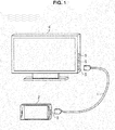
- FIG. 1 is an explanatory diagram that shows an exemplary entire configuration of a system configured by electronic devices connected with a cable according to an embodiment of the present disclosure.
- FIG. 1 an explanatory diagram that shows an exemplary entire configuration of a system configured by electronic devices connected with a cable according to an embodiment of the present disclosure.
- an exemplary entire configuration of a system according to an embodiment of the present disclosure will be described with reference to FIG. 1 .
- a system includes a source device 2 and a sink device 4.
- the source device 2 and the sink device 4 are connected with a cable 1.
- the source device 2 illustrates a compact mobile device such as a smart phone or a digital camera in FIG. 1 .
- the sink device 4 illustrates a television receiver in FIG. 1 .
- the source device 2 is provided with a source device side receptacle 3 for connecting the cable 1
- the sink device 4 is provided with a sink device side receptacle 5 for connecting the cable 1.
- the source device 2 and the sink device 4, which are shown in FIG. 1 are only an example, and the source device 2 and the sink device 4 are not limited to those shown in FIG. 1 .
- FIG. 1 a situation where the sink device 4 is provided with a plurality of the sink device side receptacles 5 (three in the drawing) is shown in FIG. 1 , it goes without saying that the present disclosure is not limited to such an example.
- source and sink are used under a definition the same as a “source” and a “sink” in a high-definition multimedia interface (HDMI). That is, the source device 2 is a device on a side from which data are sent, and the sink device 4 is a device on a side by which the data are received. Data stored in the source device 2 are transmitted to the sink device 4 through the cable 1 when the source device 2 and the sink device 4 are connected with the cable 1.
- a side that sends data is defined as a "source” and a side that receives the data is defined as a "sink”.
- the cable 1 is a cable that connects the source device side receptacle 3 provided to the source device 2 that is an output source of a video and voice, and the sink device side receptacle 5 provided to the sink device 4.
- the cable 1 performs delivery of such as video data, voice data, other data, control signals, and electrical power between the source device 2 and the sink device 4.
- the cable 1 is provided with an optical fiber cable for performing high-speed data transmission between the source device 2 and the sink device 4. Further, the cable 1 is provided with also an electrical cable for sending and receiving electrical power between the source device 2 and the sink device 4.
- a width of the cable 1 and a size of a connector are desirable to be suppressed to a size that can be used in compact electronic devices such as digital cameras and smart phones.
- FIG. 2 is an explanatory diagram that shows an exemplary structure of the cable 1 that is used in a system according to an embodiment of the present disclosure.
- an exemplary structure of the cable 1 that is used in a system according to an embodiment of the present disclosure will be described with reference to FIG. 2 .
- the cable 1 includes two plugs 12 provided to both ends, two or more electrical contact parts 13 provided to each of the plugs 12, and a plurality of optical contact parts 14 arranged in a row with a substantial equidistance. Further, a photoelectric composite cable wire 11 described below is formed between the two plugs 12.
- the photoelectric composite cable wire 11 includes at least one, desirably a plurality of optical fiber cables and two or more electrical cables. The electrical cable is connected to the electrical contact part 13.
- the plug 12 is a plug for connecting to the source device side receptacle 3 or the sink device side receptacle 5. Therefore, a shape of the plug 12 is defined to be adaptable to shapes of the source device side receptacle 3 and the sink device side receptacle 5. Further, the electrical contact parts 13 provided to the plug 12 are provided for sending and receiving electrical power between the source device 2 and the sink device 4 as will be described below. It goes without saying that the shape of the plug 12 and a position of the electrical contact part 13 provided to the plug 12 are not limited to those shown in FIG. 2 .
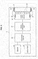
- FIG. 3 is an explanatory diagram that shows an exemplary functional configuration of the source device 2 that configures a system according to an embodiment of the present disclosure.
- an exemplary functional configuration of the source device 2 will be described with reference to FIG. 3 .
- the source device 2 that configures a system according to an embodiment of the present disclosure includes an integrated chip set 22, a memory 23, a display part 24, a signal conversion part 27 and a laser drive circuit 35. Further, the source device side receptacle 3 provided to the source device 2 includes electrical contacts 31 and 32 and a plurality of light-emitting parts 34.
- the integrated chip set 22 performs control of an operation of the source device 2. Although there are various controls of an operation of the source device 2, which the integrated chip set 22 performs, for example, the integrated chip set 22 performs various signal processes for supplying to the sink device 4 over contents such as an image and a voice, which are supplied from the source device 2 to the sink device 4.
- the memory 23 stores such as various programs that control an operation of the source device 2 and data that are used for control of the operation, and as required, the program or the data are read from the integrated chip set 22.
- the display part 24 displays images, characters and other pieces of information and includes such as a liquid crystal display and an organic EL display. The display part 24 displays images, characters and other pieces of information by the control of the integrated chip set 22.
- the signal conversion part 27 converts data of the contents such as an image and a sound into a signal for driving the laser drive circuit 35.
- a signal produced by the signal conversion part 27 is supplied to the laser drive circuit 35.
- the laser drive circuit 35 makes the light-emitting parts 34 of the source device side receptacle 3 emit light based on the signal supplied from the signal conversion part 27.
- the light-emitting part 34 emits laser light by the laser drive circuit 35.
- the light-emitting part 34 includes such as an optical member such as a vertical cavity surface emitting laser (VCSEL) element for transmitting a signal by light emission and a lens formed associatively with the VCSEL element.
- VCSEL vertical cavity surface emitting laser
- the light-emitting part 34 is provided to a position corresponding to an optical contact of the plug of the cable 1.
- the electrical contacts 31 and 32 are provided to positions that sandwich the plurality of the light-emitting parts 34 therebetween as shown in FIG. 3 .
- the electrical contact 31 is an electrical contact that imparts a predetermined potential, for example, a potential of + 5 V
- the electrical contact 32 is an electrical contact of a potential of GND.
- the electrical contact 31 that imparts a potential of + 5 V is connected with a positive electrode power supply 36 of the laser drive circuit 35, and, in the same manner, the electrical contact 32 of GND is connected to the GND 37 of the laser drive circuit 35, thus, the power supply to the laser drive circuit 35 is made possible.
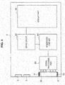
- FIG. 4 is an explanatory diagram that shows an exemplary functional configuration of the sink device 4 that configures a system according to an embodiment of the present disclosure.
- an exemplary functional configuration of the sink device 4 will be described with reference to FIG. 4 .
- the sink device 4 includes an integrated chip set 42, a drive circuit 43, a display part 44, and a signal processing part 53. Further, the sink device side receptacle 5 includes electrical contacts 51 and 52, and a plurality of light-receiving parts 54.
- the integrated chip set 42 controls an operation of the sink device 4.
- the integrated chip set 42 performs a signal process for displaying data of contents of an image and a voice transmitted from the source device 2 through the cable 1 on the display part 44, and supplies to the drive circuit 43.
- the drive circuit 43 acquires the signal from the integrated chip stet 42 and produces a signal for driving the display part 44.
- the display part 44 includes such as a liquid crystal display or an organic EL display and displays an image when driven by the drive circuit 43.
- the sink device 4 includes, as shown in FIG. 4 , one or a plurality of the sink device side receptacles 5, and, each of the sink device side receptacles 5 includes a plurality of the light-receiving parts 54 due to a photodiode element for transmitting a signal by receiving light and an optical member such as a lens that is formed associatively with the photodiode element so as to correspond to the optical contact of the plug of the cable 1.
- the electrical contacts 51 and 52 are provided with the light-receiving parts 54 interposed therebetween.
- the electrical contact 51 is an electrical contact that imparts a potential of, for example, + 5 V
- the electrical contact 52 is an electrical contact that imparts a potential of GND.
- the sink device 4 is capable of supplying electric power to the source device 2 by the contact of the electrical contacts 51 and 52 and the electrical contact parts 13 of the plug 12.
- the contents of such as an image and a voice that are transmitted through the cable 1 and supplied by the source device 2 are guided as an optical signal by an optical fiber core wire 17 of each channel of the cable 1 described below.
- the optical signal guided by the optical fiber core wire 17 is optically coupled respectively with the light-receiving part 54 of each channel corresponding to the optical contact part 14 of each channel described below.
- the signal from the light-receiving part 54 undergoes a signal process at the integrated chip set 42 after processes such as amplification and parallelization have been performed at, for example, the signal processing part 53.
- the integrated chip set 42 supplies the signal after signal process to the drive circuit 43, and the drive circuit 43 converts into a signal appropriate for driving the display part 44. Then, the content of the image transmitted from the source device 2 is displayed on the display part 44, and the voice transmitted from the source device 2 is sounded by a not shown speaker.
- FIG. 5 is an explanatory diagram that shows power supply from the sink device 4 to the source device 2 through the cable 1.
- light emission and power supply of the source device 2 due to the power supply through the cable 1 will be described with reference to FIG. 5 .
- the cable 1 is provided with two plugs 12 at both ends and each plug 12 is provided with two or more electrical contact parts 13.
- the cable 1 is provided with two or more electrical cables 15 that connect between the electrical contact parts 13 provided to the plugs 12 at both ends.
- the sink device 4 includes, as described above, the electrical contacts 51 and 52 in the sink device side receptacle 5.
- the electrical contact 51 is an electrical contact that imparts a potential of, for example, + 5 V
- the electrical contact 52 is an electrical contact of a potential of GND.
- the electrical contact parts 13 come into contact with the electrical contacts 31 and 32. By the contact, a potential of + 5 V is imparted to the laser drive circuit 35 on the source device side. In the same manner, also the GND side is connected through the electrical cable 15 of the cable 1. Therefore, by power supply from the sink device 4, the light-emitting part 34 of the source device 2 becomes capable of being driven.
- the source device 2 and the sink device 4 are connected with the cable 1, by use of the electrical cable 15 provided to the cable 1, the power supply to the source device 2, or, when the source device 2 is provided with a battery, also charging to the battery becomes possible.
- FIG. 6 is a flow chart that shows exemplary operations of the source device 2 and the sink device 4 when the source device 2 and the sink device 4 are connected with the cable 1 in a system according to an embodiment of the present disclosure.
- FIG. 6 exemplary operations of the source device 2 and the sink device 4 when the source device 2 and the sink device 4 are connected with the cable 1 will be described.
- the sink device 4 is in a standby mode (step S101). In a state in the standby mode, the electrical contact 51 on a + 5 V side of the sink device 4 is normally in a small current mode.
- the source device 2 and the sink device 4 stand by until the source device 2 and the sink device 4 are connected with the cable 1 (step S102).
- the sink device 4 detects connection with the source device 2 through the cable 1 by detecting that a current flowed between the electrical contact 51 on the + 5 V side and the electrical contact 52 on the GND side (step S103).
- the electrical contact 51 on the + 5 V side of the sink device 4 side enters into a mode capable of supplying a specified current value larger than that during the standby mode by the connection of the source device 2 and the sink device 4 with the cable 1.
- the sink device 4 sends a pulse for notifying that a preparation for power supply from the sink device 4 to a line to which + 5 V is supplied of the electrical cables 15 has been completed to the source device 2 (step S104).
- the source device 2 that has received the pulse for notifying the completion of preparation of the power supply from the sink device 4 obtains a specified current value from the electrical contact 31 on the + 5 V power supply side and drives the laser drive circuit 35 (step S105). Further, when the source device 2 receives power supply from the sink device 4, the source device 2 enters into a mode for receiving the power supply from the sink device 4 (step S106).
- the sink device 4 that has detected the connection with the source device 2 through the cable 1 controls from, for example, the integrated chip set 42 such that a circuit of the light-receiving part 54 of the sink device side receptacle 5 is activated (step S107).
- the connection by the electrical cable 15 becomes open when the cable 1 came off, and a current is not supplied from the sink device 4 to the source device 2. Therefore, oscillation of the laser light from the light emitting part 34 of the source device side receptacle 3 stops.
- the sink device 4 that has detected the connection through the cable 1 may make active, in the first stage when the light-receiving parts 54 of the sink device side receptacle 5 are activated, firstly only predetermined prioritized one channel among the plurality of the light-receiving parts 54 of the sink device 4. Further, in a signal from the light-emitting part 34 of the source device 2, which corresponds to the prioritized one channel among the light-receiving parts 54, a designation signal that designates a channel that is scheduled to be actually used may be added.
- the prioritized one channel among the light-receiving parts 54 of the sink device 4 receives the designation signal that designates channels scheduled to be actually used from the light-emitting part 34, only the light-receiving parts 54 corresponding to channels only of additionally necessary number, which are designated by the designation signal may be activated.
- the source device 2 and the sink device 4 are operated like this, since only the light-receiving parts necessary for transmitting data between the source device 2 and the sink device 4 are energized, and unnecessary light-receiving parts are not energized, power consumption may be suppressed. Further, when the source device 2 and the sink device 4 are configured like this, low consumption power during standby and low consumption power due to partial drive of only a necessary part of channels can be yielded.
- a case where only a part of the channels is partially driven for example, a case where a bit rate of a signal that is transmitted from the source device 2 to the sink device 4 is low is considered.
- the bit rate of a signal transmitted from the source device 2 to the sink device 4 is low, there is no need of driving all channels, and, only by driving minimum channels appropriate for the bit rate of the signal, a signal is transmitted from the source device 2 to the sink device 4.
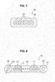
- FIG. 7 is an explanatory diagram that shows an exemplary shape of a general optical ribbon
- FIG. 8 is an explanatory diagram that shows an exemplary cross-section of the cable 1.
- the optical ribbon 19 is configured by arranging a plurality of optical fiber core wires 17 in a row and by covering the plurality of optical fiber core wires 17 with a resinous covering 18 for protecting the optical fiber core wires 17 arranged in a row.
- the number of the optical fiber core wires 17 although, for example, 2 cores, 4 cores, 8 cores, and 12 cores are generally considered, the number of the optical fiber core wires 17 is not limited to these.
- the photoelectric composite cable wire 11 that connects two plugs 12 includes electrical cables 15 with the plurality of the optical fiber core wires 17 interposed therebetween as shown in FIG. 8 . Further, when a cross section of the photoelectric composite cable wire 11 is viewed, as shown in FIG. 8 , diameters or thicknesses ⁇ D of covering parts 16 of the electrical cables 15 that sandwich the optical fiber core wires 17 are thicker than a thickness dimension t of the covering 18 of a part of the optical fiber core wires 17.
- the cable 1 When the cable 1 is configured like this, the following advantageous effects are yielded. Firstly, when the photoelectric composite cable wire 11 always comes into contact with a plane such as a floor or a table, the covering part of the electrical cable 15 comes into contact, therefore, an advantageous effect that it becomes difficult to impart an external damage to the optical fiber core wires 17 and the covering 18 of the optical fiber core wires is yielded.
- FIG. 9, FIG. 10 and FIG. 11 each is an explanatory diagram that shows a case where the photoelectric composite cable wire 11 is twisted, laterally bent, or vertically bent.
- maximum displacement and force F are in proportion to a distance of an axis that is a center of bending.
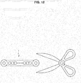
- FIG. 12 is an explanatory diagram that shows a situation where the cable 1 is about to be cut with a pair of scissors. As shown in FIG. 12 , also when the cable 1 is cut with, for example, a pair of scissors, a cutter, or a sharp corner, a peripheral electrical cable 15 and the covering part 16 of the electrical cable 15 are initially cut. Therefore, the optical fiber core wires 17 and the covering 18 of the optical fiber core wires are cut after the electrical cable 15 and the covering part 16 of the electrical cable 15 are cut.
- the photoelectric composite cable wire 11 is cut in a state where the source device 2 and the sink device 4 are connected with the cable 1, the electrical cable 15 is cut in advance, therefore, the power supply from the sink device 4 to the source device 2 is stopped and oscillation (light emission) of the laser light of the source device 2 is stopped. That is, in a state where the cable 1 is entirely or partially cut, an infrared ray or visible light that may be detrimental to human eye due to high energy density does not come out of a cut plane of the cable 1. Further, in the same manner, also when the plug 12 is not inserted in the sink device side receptacle 5, the infrared ray or the visible light does not come out from an end plane of the plug 12 or the optical contact part 14. Therefore, even when the photoelectric composite cable wire 11 is cut in a state where the source device 2 and the sink device 4 are connected with the cable 1, the eye safety is yielded.
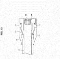
- FIG. 13 is an explanatory diagram that conceptually shows a certain exemplary structure of the plug 12 of the cable 1.
- FIG. 14 is an explanatory diagram that shows a plan view and a front view of another exemplary structure of the plug 12.
- the photoelectric composite cable wire 11 is provided with the electrical cables 15 with the plurality of optical fiber core wires 17 interposed therebetween. Therefore, as a structure of the plug 12, a shape that is shown in, for example, FIG. 13 is considered.
- FIG. 13 shows an internal structure of the plug 12.
- a plurality of the optical fiber core wires 17 are arranged in a row, and in front of the optical fiber core wires 17, a member of the optical contact parts 14 is provided.
- FIG. 14 shows another exemplary structure of the plug 12.
- the plurality of the optical fiber core wires 17 are arranged in a row, and in front thereof, the member of the optical contact parts 14 is formed with positioning hole parts 61 and 62 provided on both sides.
- FIG. 14 illustrates only a right half of the plug 12 such that an internal structure of the plug 12 may be well understood.
- the electrical contact parts 13 with a spring element are configured so as to come into the positioning hole parts 61 and 62 from a side surface on an opposite side of a side where the optical fiber core wires 17 are present of the positioning hole parts 61 and 62.
- the member of the optical contact parts 14 is formed by integrally molding the plurality of channels in a row, a form of the optical contact part in the cable of the present disclosure is not limited to such examples.
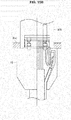
- FIG. 15A and FIG. 15B each is an explanatory diagram that shows a situation where the plug 12 and the source device side receptacle 3 of the source device 2, or the sink device side receptacle 5 of the sink device 5 are joined in a plan view.
- the FIG. 15A and FIG. 15B each shows only a right half of the plug 12 such that an internal structure of the plug 12 may be well understood.
- FIG. 15A shows a state before the plug 12 and the source device side receptacle 3 of the source device 2, or the sink device side receptacle 5 of the sink device 5 are joined.
- FIG. 15B shows a state after the plug 12 and the source device side receptacle 3 of the source device 2, or the sink device side receptacle 5 of the sink device 5 have been joined.
- Positioning pins 63 and 64 are provided to the source device side receptacle 3 or the sink device side receptacle 5.
- the positioning pins 63 and 64 are electrical contacts of the source device side receptacle 3 or the sink device side receptacle 5.
- the positioning pins 63 and 64 are inserted into the positioning hole parts 61 and 62 of the plug 12, and by the contact with the electrical contact parts 13 with a spring element, electrical continuation is established and positioning is performed with respect to an insertion direction.
- the optical contact part 14 of the plug 12 is positioned with respect to the light-emitting part 34 of the source device 2 or the light-receiving part 54 of the sink device 4, an optical communication is performed between the source device 2 and the sink device 4.
- the plug 12 configured like this separates, at the time of assembling, two electrical cables 15 (including covering) which are externally disposed in the optical composite cable wire 11, and the optical ribbon 19 into three at the root of the plug 12. Then, the electrical cable 15 is, after the covering has been peeled, electrically joined with the electrical contact part 13 positioned outside of the plurality of optical fiber core wires 17 by means of such as caulking. On the other hand, the plurality of the optical fiber core wires 17 in the center part become a plurality of optical contact parts 14 that are arranged with the same pitch as that (distance between core wires) of the optical fiber core wires.
- the optical fiber core wires 17 and the integrally molded optical contact parts having such as lenses for condensing light of a plurality of channels arranged with the same pitch may have a configuration in which these are adhered by facing with a distance or by facing without a distance by use of such as an adhesive.
- a size of the plug 12 of the cable 1 is desirable to be formed into a relatively small size, for example, a size identical with a micro-universal serial bus (USB) terminal, or a size smaller than that.
- USB micro-universal serial bus
- the shape of the plug 12 shown in FIG. 14 is an example and the shape of the plug of the cable is not limited to such an example in the present disclosure.
- a form of a cable of the present disclosure is not limited to the form described above.
- the present disclosure is not limited to such an example.
- Three, four or more electrical contact parts 13 may be provided to the plug 12.
- a signal for example, on a + 5 V side as a minute differential signal
- a signal of an existing electrical interface such as a past mobile high-definition link (MHL) may be flowed through the electrical contact part 13.
- MHL mobile high-definition link
- the electrical contact part 13 may have a structure in which overall positioning is performed with a polishing shaft.
- the polishing shaft may be provided with a groove for providing a click feeling at the time of joining or for calling in compression molding.
- the optical ribbon 19 is not necessarily arranged in a row.
- the 12 cores may be arranged in a row, or in 3 rows of 4 cores.
- the plug 12 may be configured also by facing the plurality of the optical fiber core wires 17 and the plurality of the optical contact parts 14 that are arranged with the same pitch as that (distance between core wires) of the plurality of the optical fiber core wires 17.
- the photoelectric composite interface and the cable 1 used in the photoelectric composite interface may be configured as described above.
- the cable 1, the source device side receptacle 3 of the source device 2 and the sink device side receptacle 5 of the sink device 4 are formed into forms as described above, an interface for a not-existing CE device, which is capable of performing communication at a ultra-high-speed from several tens of Gbps to exceeding 100 Gbps, which has been very difficult to yield in an existing interface between devices due to only electricity is yielded.
- optical fibers incorporated in the cable are suppressed from breaking, the eye safety from a laser light used in communication is yielded, and low consumption power of the source device is yielded. Further, downsizing and thinning of the plug of the cable 1 are yielded, and by reducing an assemblage cost, manufacture at low cost is yielded.
- the cable 1, the source device 2 and the sink device 4 are capable of providing a safe and inexpensive novel photoelectric composite interface corresponding to a rise in a transmission speed of a non-compressed signal accompanying high pixelization of a future display.
- present technology may also be configured as below.
- a cable including:
- An electronic device including:
- the electronic device according to (8), wherein the light emission control part makes light emit only from the minimum light-emitting parts necessary for communication with the partner side electronic device at the time when control of emission of laser light from the light-emitting part is started.
- An electronic device including:
- a method for controlling an electronic device including:
- a method for controlling an electronic device including:
Abstract
Description
- The present disclosure relates to a cable, an electronic device and a method for controlling the electronic device.
- Recently, an advancement of technology of high pixelization of a display device is in progress, and trends of the advancement of the technology of high pixelization of a display device are expected to continue further. Therefore, a demand for a transmission speed of non-compressed signals to the display device is increasing in proportion to an increase in the number of pixels of the display device.
- In a television, for example, a replacement from a standard image quality (SD image quality) of such as 720 horizontal pixels by 480 vertical pixels to a high definition image quality (HD image quality) of such as 1920 horizontal pixels by 1080 vertical pixels is in progress. However, research and development of an image resolution of around 4,000 horizontal pixels by around 2,000 vertical pixels, which is so-called as 4K2K, and, furthermore, also a ultrahigh definition television (UHDTV) that is also called a super-high vision of 7,680 horizontal pixels by 4,320 vertical pixels are in progress.
- In the 4K2K, a transmission speed of 4 times a transmission speed of the HD image quality is necessary and, in the UHDTV, the transmission speed of 48 times the transmission speed of the HD image quality is necessary. In the transmission speeds like this, there is a problem that transmission of non-compressed video signals due to a past copper wire line is not realistic. Therefore, it is considered that transmission by an optical fiber cable becomes general in the same manner as in the other high-speed data communication such as 100 G bit ETHERNET standard.
- Patent Literature 1:
JP 2010-237640A - On the other hand, there does not exist a typical standard of a high-speed optical interface of about 10 Gbps or more, which is mainly used in consumer electronics (CE) devices. Although a composite cable that accommodates an electric wire and an optical fiber has been proposed as in, for example, the
Patent Literature 1, it cannot be said that optical interfaces for use in infrastructures or managements including present INTERNET have yielded eye-safety from laser light, realistic low cost and a magnitude corresponding to recent compact devices, which are required for the CE devices. Therefore, in view of the trends of high-pixelization of the display devices, an optical interface that is safe, inexpensive and compact, and is mainly used in the CE devices is in demand. - Therefore, the present disclosure intends to provide a novel and improved photoelectric composite cable that is capable of yielding an optical interface that is safe, inexpensive, and compact; and is capable of high-speed transmission, an electronic device and a method for controlling the electronic device.
- According to the present disclosure, there is provided a cable including at least one optical fiber cable, at least two electrical cables provided so as to sandwich the optical fiber cable, and plugs positioned at both ends and each having an electrical contact part connected to each of the electrical cables.
- According to the present disclosure, there is provided an electronic device including a receptacle having at least two electrical contacts and at least one light-emitting part configured to emit laser light for performing communication by light to a partner side electronic device, and a light emission control part configured to control emission of laser light from the light-emitting part. The light emission control part starts control of emission of laser light from the light-emitting part by a current when a cable is connected to the receptacle and the current flows to the electrical contacts from the partner side electronic device.
- According to the present disclosure, there is provided an electronic device including a receptacle having at least two electrical contacts and at least one light-receiving part configured to receive laser light for performing communication by light emitted from a partner side electronic device, and a supply control part configured to control supply of a current to the partner side electronic device through the electrical contacts. The supply control part starts supply of a current through the electrical contacts when a cable is connected to the receptacle.
- According to the present disclosure, there is provided a method for controlling an electronic device, the method including a step of starting control of emission of laser light from a light-emitting part by a current when a cable is connected to a receptacle having at least two electrical contacts and at least one light-emitting part configured to emit laser light for performing communication by light to a partner side electronic device, and the current flows from the partner side electronic device to the electrical contacts.
- According to the present disclosure, there is provided a method for controlling an electronic device, the method including a step of starting supply of a current to a partner side electronic device through electrical contacts when a cable is connected to a receptacle having at least two electrical contacts and at least one light-receiving part configured to receive laser light for performing communication by light emitted from the partner side electronic device.
- As described above, according to the present disclosure, the present disclosure is capable of providing a novel and improved cable that is capable of yielding an optical interface that is safe, inexpensive, and compact, and is capable of high-speed transmission, an electronic device and a method for controlling the electronic device.
-
- [
FIG. 1] FIG. 1 is an explanatory diagram that shows an exemplary entire configuration of a system configured by electronic devices connected with a cable according to an embodiment of the present disclosure. - [
FIG. 2] FIG. 2 is an explanatory diagram that shows an exemplary structure of acable 1 that is used in a system according to an embodiment of the present disclosure. - [
FIG. 3] FIG. 3 is an explanatory diagram that shows an exemplary functional configuration of asource device 2 that configures a system according to an embodiment of the present disclosure. - [
FIG. 4] FIG. 4 is an explanatory diagram that shows an exemplary functional configuration of asink device 4 that configures a system according to an embodiment of the present disclosure. - [
FIG. 5] FIG. 5 is an explanatory diagram that shows power supply from thesink device 4 to thesource device 2 through thecable 1. - [
FIG. 6] FIG. 6 is a flow chart that shows exemplary operations of thesource device 2 and thesink device 4. - [
FIG. 7] FIG. 7 is an explanatory diagram that shows an exemplary shape of a general optical ribbon. - [
FIG. 8] FIG. 8 is an explanatory diagram that shows an exemplary cross-section of thecable 1. - [
FIG. 9] FIG. 9 is an explanatory diagram that shows a case where a photoelectriccomposite cable wire 11 is twisted. - [
FIG.10] FIG. 10 is an explanatory diagram that shows a case where the photoelectriccomposite cable wire 11 is laterally bent. - [
FIG. 11] FIG. 11 is an explanatory diagram that shows a case where the photoelectriccomposite cable wire 11 is vertically bent. - [
FIG. 12] FIG. 12 is an explanatory diagram that shows a situation where thecable 1 is about to be cut with a pair of scissors. - [
FIG. 13] FIG. 13 is an explanatory diagram that conceptually shows a structure of aplug 12 of thecable 1. - [
FIG. 14] FIG. 14 is an explanatory diagram that shows a plan view and a front view of an exemplary configuration of theplug 12. - [
FIG. 15A] FIG. 15A is an explanatory diagram that shows a situation where a plug and a receptacle are joined. - [
FIG. 15B] FIG. 15B is an explanatory diagram that shows a situation where a plug and a receptacle are joined. - Hereinafter, preferred embodiments of the present disclosure will be described in detail with reference to the appended drawings. Note that, in this specification and the drawings, elements that have substantially the same function and structure are denoted with the same reference signs, and repeated explanation is omitted.
- Note that description will be provided in the following order.
- [Exemplary System Configuration]
[Exemplary Structure of Cable]
[Exemplary Functional Configuration of Source Device]
[Exemplary Functional Configuration of Sink Device]
[Power Supply through Cable]
[Exemplary Operations of Source Device and Sink Device]
[Exemplary Shape of Cable] - Firstly, an exemplary entire configuration of a system according to an embodiment of the present disclosure will be described.
FIG. 1 is an explanatory diagram that shows an exemplary entire configuration of a system configured by electronic devices connected with a cable according to an embodiment of the present disclosure. Hereinafter, an exemplary entire configuration of a system according to an embodiment of the present disclosure will be described with reference toFIG. 1 . - As shown in
FIG. 1 , a system according to an embodiment of the present disclosure includes asource device 2 and asink device 4. Thesource device 2 and thesink device 4 are connected with acable 1. - The
source device 2 illustrates a compact mobile device such as a smart phone or a digital camera inFIG. 1 . Thesink device 4 illustrates a television receiver inFIG. 1 . Thesource device 2 is provided with a sourcedevice side receptacle 3 for connecting thecable 1, and thesink device 4 is provided with a sinkdevice side receptacle 5 for connecting thecable 1. It goes without saying that thesource device 2 and thesink device 4, which are shown inFIG. 1 are only an example, and thesource device 2 and thesink device 4 are not limited to those shown inFIG. 1 . Further, although a situation where thesink device 4 is provided with a plurality of the sink device side receptacles 5 (three in the drawing) is shown inFIG. 1 , it goes without saying that the present disclosure is not limited to such an example. - Here, terms of "source" and "sink" are used under a definition the same as a "source" and a "sink" in a high-definition multimedia interface (HDMI). That is, the
source device 2 is a device on a side from which data are sent, and thesink device 4 is a device on a side by which the data are received. Data stored in thesource device 2 are transmitted to thesink device 4 through thecable 1 when thesource device 2 and thesink device 4 are connected with thecable 1. In the following explanation, a side that sends data is defined as a "source" and a side that receives the data is defined as a "sink". - The
cable 1 is a cable that connects the sourcedevice side receptacle 3 provided to thesource device 2 that is an output source of a video and voice, and the sinkdevice side receptacle 5 provided to thesink device 4. Thecable 1 performs delivery of such as video data, voice data, other data, control signals, and electrical power between thesource device 2 and thesink device 4. Thecable 1 is provided with an optical fiber cable for performing high-speed data transmission between thesource device 2 and thesink device 4. Further, thecable 1 is provided with also an electrical cable for sending and receiving electrical power between thesource device 2 and thesink device 4. A width of thecable 1 and a size of a connector are desirable to be suppressed to a size that can be used in compact electronic devices such as digital cameras and smart phones. - In the above, an exemplary entire configuration of a system according to an embodiment of the present disclosure has been described with reference to
FIG. 1 . Next, an exemplary structure of a cable used in a system according to an embodiment of the present disclosure will be described. -
FIG. 2 is an explanatory diagram that shows an exemplary structure of thecable 1 that is used in a system according to an embodiment of the present disclosure. Hereinafter, an exemplary structure of thecable 1 that is used in a system according to an embodiment of the present disclosure will be described with reference toFIG. 2 . - As shown in
FIG. 2 , thecable 1 includes twoplugs 12 provided to both ends, two or moreelectrical contact parts 13 provided to each of theplugs 12, and a plurality ofoptical contact parts 14 arranged in a row with a substantial equidistance. Further, a photoelectriccomposite cable wire 11 described below is formed between the two plugs 12. The photoelectriccomposite cable wire 11 includes at least one, desirably a plurality of optical fiber cables and two or more electrical cables. The electrical cable is connected to theelectrical contact part 13. - The
plug 12 is a plug for connecting to the sourcedevice side receptacle 3 or the sinkdevice side receptacle 5. Therefore, a shape of theplug 12 is defined to be adaptable to shapes of the sourcedevice side receptacle 3 and the sinkdevice side receptacle 5. Further, theelectrical contact parts 13 provided to theplug 12 are provided for sending and receiving electrical power between thesource device 2 and thesink device 4 as will be described below. It goes without saying that the shape of theplug 12 and a position of theelectrical contact part 13 provided to theplug 12 are not limited to those shown inFIG. 2 . - When a high-speed and large capacity digital signal of 10 Gbps per one channel is assumed to be flowed to the photoelectric
composite cable wire 11 shown inFIG. 2 , by using an optical fiber having a plurality of channels (the number of channels) as the photoelectriccomposite cable wire 11, signals corresponding to multiple number of the channel number can be transmitted. That is, ultra-high-speed communication from several tens of Gbps to exceeding 100 Gbps, which has been very difficult to yield with a past inter-device interface due to only electricity becomes possible. - In the above, an exemplary structure of the
cable 1 used in a system according to an embodiment of the present disclosure has been described with reference toFIG. 2 . Next, an exemplary functional configuration of thesource device 2 that configures a system according to an embodiment of the present disclosure will be described. -
FIG. 3 is an explanatory diagram that shows an exemplary functional configuration of thesource device 2 that configures a system according to an embodiment of the present disclosure. Hereinafter, an exemplary functional configuration of thesource device 2 will be described with reference toFIG. 3 . - As shown in
FIG. 3 , thesource device 2 that configures a system according to an embodiment of the present disclosure includes an integrated chip set 22, amemory 23, adisplay part 24, asignal conversion part 27 and alaser drive circuit 35. Further, the sourcedevice side receptacle 3 provided to thesource device 2 includeselectrical contacts parts 34. - The integrated chip set 22 performs control of an operation of the
source device 2. Although there are various controls of an operation of thesource device 2, which the integrated chip set 22 performs, for example, the integrated chip set 22 performs various signal processes for supplying to thesink device 4 over contents such as an image and a voice, which are supplied from thesource device 2 to thesink device 4. Thememory 23 stores such as various programs that control an operation of thesource device 2 and data that are used for control of the operation, and as required, the program or the data are read from the integrated chip set 22. Thedisplay part 24 displays images, characters and other pieces of information and includes such as a liquid crystal display and an organic EL display. Thedisplay part 24 displays images, characters and other pieces of information by the control of the integrated chip set 22. - The
signal conversion part 27 converts data of the contents such as an image and a sound into a signal for driving thelaser drive circuit 35. A signal produced by thesignal conversion part 27 is supplied to thelaser drive circuit 35. Thelaser drive circuit 35 makes the light-emittingparts 34 of the sourcedevice side receptacle 3 emit light based on the signal supplied from thesignal conversion part 27. - The light-emitting
part 34 emits laser light by thelaser drive circuit 35. The light-emittingpart 34 includes such as an optical member such as a vertical cavity surface emitting laser (VCSEL) element for transmitting a signal by light emission and a lens formed associatively with the VCSEL element. - The light-emitting
part 34 is provided to a position corresponding to an optical contact of the plug of thecable 1. Theelectrical contacts parts 34 therebetween as shown inFIG. 3 . Theelectrical contact 31 is an electrical contact that imparts a predetermined potential, for example, a potential of + 5 V, and theelectrical contact 32 is an electrical contact of a potential of GND. When theplug 12 of thecable 1 is engaged with the sourcedevice side receptacle 3, theelectrical contacts electrical contact parts 13 of theplug 12 come into contact. Thesource device 2 is capable of receiving a supply of electric power from thesink device 4 by the contact of theelectrical contacts electrical contact parts 13 of theplug 12. - The
electrical contact 31 that imparts a potential of + 5 V is connected with a positiveelectrode power supply 36 of thelaser drive circuit 35, and, in the same manner, theelectrical contact 32 of GND is connected to theGND 37 of thelaser drive circuit 35, thus, the power supply to thelaser drive circuit 35 is made possible. - In the above, an exemplary functional configuration of the
source device 2 has been described with reference toFIG. 3 . Next, an exemplary functional configuration of thesink device 4 that configures a system according to an embodiment of the present disclosure will be described. -
FIG. 4 is an explanatory diagram that shows an exemplary functional configuration of thesink device 4 that configures a system according to an embodiment of the present disclosure. Hereinafter, an exemplary functional configuration of thesink device 4 will be described with reference toFIG. 4 . - As shown in
FIG. 4 , thesink device 4 includes an integrated chip set 42, adrive circuit 43, adisplay part 44, and asignal processing part 53. Further, the sinkdevice side receptacle 5 includeselectrical contacts parts 54. - The integrated chip set 42 controls an operation of the
sink device 4. For example, the integrated chip set 42 performs a signal process for displaying data of contents of an image and a voice transmitted from thesource device 2 through thecable 1 on thedisplay part 44, and supplies to thedrive circuit 43. Thedrive circuit 43 acquires the signal from the integratedchip stet 42 and produces a signal for driving thedisplay part 44. Thedisplay part 44 includes such as a liquid crystal display or an organic EL display and displays an image when driven by thedrive circuit 43. - The
sink device 4 includes, as shown inFIG. 4 , one or a plurality of the sinkdevice side receptacles 5, and, each of the sinkdevice side receptacles 5 includes a plurality of the light-receivingparts 54 due to a photodiode element for transmitting a signal by receiving light and an optical member such as a lens that is formed associatively with the photodiode element so as to correspond to the optical contact of the plug of thecable 1. Theelectrical contacts parts 54 interposed therebetween. Theelectrical contact 51 is an electrical contact that imparts a potential of, for example, + 5 V, and theelectrical contact 52 is an electrical contact that imparts a potential of GND. When theplug 12 of thecable 1 is engaged with the sinkdevice side receptacle 5, theelectrical contacts electrical contact parts 13 of theplug 12 come into contact. Thesink device 4 is capable of supplying electric power to thesource device 2 by the contact of theelectrical contacts electrical contact parts 13 of theplug 12. - The contents of such as an image and a voice that are transmitted through the
cable 1 and supplied by thesource device 2 are guided as an optical signal by an opticalfiber core wire 17 of each channel of thecable 1 described below. The optical signal guided by the opticalfiber core wire 17 is optically coupled respectively with the light-receivingpart 54 of each channel corresponding to theoptical contact part 14 of each channel described below. - The signal from the light-receiving
part 54 undergoes a signal process at the integrated chip set 42 after processes such as amplification and parallelization have been performed at, for example, thesignal processing part 53. The integrated chip set 42 supplies the signal after signal process to thedrive circuit 43, and thedrive circuit 43 converts into a signal appropriate for driving thedisplay part 44. Then, the content of the image transmitted from thesource device 2 is displayed on thedisplay part 44, and the voice transmitted from thesource device 2 is sounded by a not shown speaker. - In the above, an exemplary functional configuration of the
sink device 4 has been described with reference toFIG. 4 . Next, light emission and power supply of thesource device 2 due to power supply through thecable 1 that connects thesource device 2 and thesink device 4 will be described. -
FIG. 5 is an explanatory diagram that shows power supply from thesink device 4 to thesource device 2 through thecable 1. Hereinafter, light emission and power supply of thesource device 2 due to the power supply through thecable 1 will be described with reference toFIG. 5 . - As shown in
FIG. 2 , thecable 1 is provided with twoplugs 12 at both ends and each plug 12 is provided with two or moreelectrical contact parts 13. Thecable 1 is provided with two or moreelectrical cables 15 that connect between theelectrical contact parts 13 provided to theplugs 12 at both ends. - The
sink device 4 includes, as described above, theelectrical contacts device side receptacle 5. Theelectrical contact 51 is an electrical contact that imparts a potential of, for example, + 5 V, and theelectrical contact 52 is an electrical contact of a potential of GND. When theplug 12 is inserted into the sinkdevice side receptacle 5, theelectrical contact parts 13 come into contact with theelectrical contacts electrical cable 15 is performed from the sinkdevice side receptacle 5 to a partner side plug 12 of thecable 1 by the contact ofelectrical contacts electrical contact parts 13. - When the partner side plug 12 is inserted into the source
device side receptacle 3, theelectrical contact parts 13 come into contact with theelectrical contacts laser drive circuit 35 on the source device side. In the same manner, also the GND side is connected through theelectrical cable 15 of thecable 1. Therefore, by power supply from thesink device 4, the light-emittingpart 34 of thesource device 2 becomes capable of being driven. - Further, when the
source device 2 and thesink device 4 are connected with thecable 1, by use of theelectrical cable 15 provided to thecable 1, the power supply to thesource device 2, or, when thesource device 2 is provided with a battery, also charging to the battery becomes possible. - In the above, the light emission and power supply of the
source device 2 due to power supply through thecable 1 have been described with reference toFIG. 5 . Next, exemplary operations of thesource device 2 and thesink device 4 when thesource device 2 and thesink device 4 are connected with thecable 1 will be described. -
FIG. 6 is a flow chart that shows exemplary operations of thesource device 2 and thesink device 4 when thesource device 2 and thesink device 4 are connected with thecable 1 in a system according to an embodiment of the present disclosure. Hereinafter, with reference toFIG. 6 , exemplary operations of thesource device 2 and thesink device 4 when thesource device 2 and thesink device 4 are connected with thecable 1 will be described. - At the time of non-connection of the cable in which the
source device 2 and thesink device 4 are not connected with thecable 1, thesink device 4 is in a standby mode (step S101). In a state in the standby mode, theelectrical contact 51 on a + 5 V side of thesink device 4 is normally in a small current mode. - The
source device 2 and thesink device 4 stand by until thesource device 2 and thesink device 4 are connected with the cable 1 (step S102). When thesource device 2 and thesink device 4 are connected with thecable 1, thesink device 4 detects connection with thesource device 2 through thecable 1 by detecting that a current flowed between theelectrical contact 51 on the + 5 V side and theelectrical contact 52 on the GND side (step S103). Theelectrical contact 51 on the + 5 V side of thesink device 4 side enters into a mode capable of supplying a specified current value larger than that during the standby mode by the connection of thesource device 2 and thesink device 4 with thecable 1. - Subsequently, the
sink device 4 sends a pulse for notifying that a preparation for power supply from thesink device 4 to a line to which + 5 V is supplied of theelectrical cables 15 has been completed to the source device 2 (step S104). - The
source device 2 that has received the pulse for notifying the completion of preparation of the power supply from thesink device 4 obtains a specified current value from theelectrical contact 31 on the + 5 V power supply side and drives the laser drive circuit 35 (step S105). Further, when thesource device 2 receives power supply from thesink device 4, thesource device 2 enters into a mode for receiving the power supply from the sink device 4 (step S106). - Further, the
sink device 4 that has detected the connection with thesource device 2 through thecable 1 controls from, for example, the integrated chip set 42 such that a circuit of the light-receivingpart 54 of the sinkdevice side receptacle 5 is activated (step S107). - When the
source device 2 and thesink device 4 are driven like this, laser light is emitted from the light-emittingpart 34 of the sourcedevice side receptacle 3 only when both devices are surely connected with thecable 1. - Further, when the
source device 2 and thesink device 4 are driven like this, the connection by theelectrical cable 15 becomes open when thecable 1 came off, and a current is not supplied from thesink device 4 to thesource device 2. Therefore, oscillation of the laser light from thelight emitting part 34 of the sourcedevice side receptacle 3 stops. - That is, when the
source device 2 and thesink device 4 are not surely connected with thecable 1, a potential of + 5 V is not supplied from thesink device 4 to thesource device 2, and since the laser light is not emitted from the light-emittingpart 34, the eye safety is yielded. - In the above, exemplary operations of the
source device 2 and thesink device 4 when thesource device 2 and thesink device 4 are connected with thecable 1 have been described with reference toFIG. 6 . - Next, modified exemplary operations of the
source device 2 and thesink device 4 will be described. Thesink device 4 that has detected the connection through thecable 1 may make active, in the first stage when the light-receivingparts 54 of the sinkdevice side receptacle 5 are activated, firstly only predetermined prioritized one channel among the plurality of the light-receivingparts 54 of thesink device 4. Further, in a signal from the light-emittingpart 34 of thesource device 2, which corresponds to the prioritized one channel among the light-receivingparts 54, a designation signal that designates a channel that is scheduled to be actually used may be added. - Then, when the prioritized one channel among the light-receiving
parts 54 of thesink device 4 receives the designation signal that designates channels scheduled to be actually used from the light-emittingpart 34, only the light-receivingparts 54 corresponding to channels only of additionally necessary number, which are designated by the designation signal may be activated. - When the
source device 2 and thesink device 4 are operated like this, since only the light-receiving parts necessary for transmitting data between thesource device 2 and thesink device 4 are energized, and unnecessary light-receiving parts are not energized, power consumption may be suppressed. Further, when thesource device 2 and thesink device 4 are configured like this, low consumption power during standby and low consumption power due to partial drive of only a necessary part of channels can be yielded. - Specifically, as a case where only a part of the channels is partially driven, for example, a case where a bit rate of a signal that is transmitted from the
source device 2 to thesink device 4 is low is considered. When the bit rate of a signal transmitted from thesource device 2 to thesink device 4 is low, there is no need of driving all channels, and, only by driving minimum channels appropriate for the bit rate of the signal, a signal is transmitted from thesource device 2 to thesink device 4. - Next, an exemplary shape of the
cable 1 used in a system according to an embodiment of the present disclosure will be described.FIG. 7 is an explanatory diagram that shows an exemplary shape of a general optical ribbon, andFIG. 8 is an explanatory diagram that shows an exemplary cross-section of thecable 1. - Firstly, an exemplary shape of a general
optical ribbon 19 will be described with reference toFIG. 7 . In general, theoptical ribbon 19 is configured by arranging a plurality of opticalfiber core wires 17 in a row and by covering the plurality of opticalfiber core wires 17 with a resinous covering 18 for protecting the opticalfiber core wires 17 arranged in a row. As the number of the opticalfiber core wires 17, although, for example, 2 cores, 4 cores, 8 cores, and 12 cores are generally considered, the number of the opticalfiber core wires 17 is not limited to these. - Next, an exemplary cross section of the
cable 1 will be described with reference toFIG. 8 . The photoelectriccomposite cable wire 11 that connects twoplugs 12 includeselectrical cables 15 with the plurality of the opticalfiber core wires 17 interposed therebetween as shown inFIG. 8 . Further, when a cross section of the photoelectriccomposite cable wire 11 is viewed, as shown inFIG. 8 , diameters or thicknesses Φ D of coveringparts 16 of theelectrical cables 15 that sandwich the opticalfiber core wires 17 are thicker than a thickness dimension t of the covering 18 of a part of the opticalfiber core wires 17. - When the
cable 1 is configured like this, the following advantageous effects are yielded. Firstly, when the photoelectriccomposite cable wire 11 always comes into contact with a plane such as a floor or a table, the covering part of theelectrical cable 15 comes into contact, therefore, an advantageous effect that it becomes difficult to impart an external damage to the opticalfiber core wires 17 and the covering 18 of the optical fiber core wires is yielded. - Further, there is an advantageous effect that a role as a mechanical holding member (tension member) when the photoelectric
composite cable wire 11 is pulled may be imparted to theelectrical cables 15.FIG. 9, FIG. 10 and FIG. 11 each is an explanatory diagram that shows a case where the photoelectriccomposite cable wire 11 is twisted, laterally bent, or vertically bent. As shown inFIG. 9, FIG. 10 and FIG. 11 , together with the role as the mechanical holding member, in all cases where the photoelectriccomposite cable wire 11 is twisted, laterally or vertically bent, maximum displacement and force F are in proportion to a distance of an axis that is a center of bending. Therefore, since in all cases where the photoelectriccomposite cable wire 11 is twisted, laterally or vertically bent, the maximum displacement and force F are applied to theelectrical cable 15 and the coveringpart 16 of theelectrical cable 15, an advantageous effect that excessive stress is capable of being prevented from occurring to the opticalfiber core wires 17 and the covering 18 of the opticalfiber core wires 17 is capable of yielding to thecable 1. -
FIG. 12 is an explanatory diagram that shows a situation where thecable 1 is about to be cut with a pair of scissors. As shown inFIG. 12 , also when thecable 1 is cut with, for example, a pair of scissors, a cutter, or a sharp corner, a peripheralelectrical cable 15 and the coveringpart 16 of theelectrical cable 15 are initially cut. Therefore, the opticalfiber core wires 17 and the covering 18 of the optical fiber core wires are cut after theelectrical cable 15 and the coveringpart 16 of theelectrical cable 15 are cut. - As described above, when the photoelectric
composite cable wire 11 is cut in a state where thesource device 2 and thesink device 4 are connected with thecable 1, theelectrical cable 15 is cut in advance, therefore, the power supply from thesink device 4 to thesource device 2 is stopped and oscillation (light emission) of the laser light of thesource device 2 is stopped. That is, in a state where thecable 1 is entirely or partially cut, an infrared ray or visible light that may be detrimental to human eye due to high energy density does not come out of a cut plane of thecable 1. Further, in the same manner, also when theplug 12 is not inserted in the sinkdevice side receptacle 5, the infrared ray or the visible light does not come out from an end plane of theplug 12 or theoptical contact part 14. Therefore, even when the photoelectriccomposite cable wire 11 is cut in a state where thesource device 2 and thesink device 4 are connected with thecable 1, the eye safety is yielded. - Subsequently, an exemplary structure of the
plugs 12 provided to both ends of thecable 1 will be described.FIG. 13 is an explanatory diagram that conceptually shows a certain exemplary structure of theplug 12 of thecable 1. Further,FIG. 14 is an explanatory diagram that shows a plan view and a front view of another exemplary structure of theplug 12. As described above, the photoelectriccomposite cable wire 11 is provided with theelectrical cables 15 with the plurality of opticalfiber core wires 17 interposed therebetween. Therefore, as a structure of theplug 12, a shape that is shown in, for example,FIG. 13 is considered. -
FIG. 13 shows an internal structure of theplug 12. In an example shown inFIG. 13 , a plurality of the opticalfiber core wires 17 are arranged in a row, and in front of the opticalfiber core wires 17, a member of theoptical contact parts 14 is provided. -
FIG. 14 shows another exemplary structure of theplug 12. In theplug 12 shown inFIG. 14 , the plurality of the opticalfiber core wires 17 are arranged in a row, and in front thereof, the member of theoptical contact parts 14 is formed withpositioning hole parts FIG. 14 illustrates only a right half of theplug 12 such that an internal structure of theplug 12 may be well understood. As shown inFIG. 14 , theelectrical contact parts 13 with a spring element are configured so as to come into thepositioning hole parts fiber core wires 17 are present of thepositioning hole parts FIG. 13 andFIG. 14 , although the member of theoptical contact parts 14 is formed by integrally molding the plurality of channels in a row, a form of the optical contact part in the cable of the present disclosure is not limited to such examples. - Next, joining of the
plug 12 and the sourcedevice side receptacle 3 of thesource device 2, or the sinkdevice side receptacle 5 of thesink device 5 will be described.FIG. 15A andFIG. 15B each is an explanatory diagram that shows a situation where theplug 12 and the sourcedevice side receptacle 3 of thesource device 2, or the sinkdevice side receptacle 5 of thesink device 5 are joined in a plan view. TheFIG. 15A andFIG. 15B each shows only a right half of theplug 12 such that an internal structure of theplug 12 may be well understood.FIG. 15A shows a state before theplug 12 and the sourcedevice side receptacle 3 of thesource device 2, or the sinkdevice side receptacle 5 of thesink device 5 are joined.FIG. 15B shows a state after theplug 12 and the sourcedevice side receptacle 3 of thesource device 2, or the sinkdevice side receptacle 5 of thesink device 5 have been joined. - Positioning pins 63 and 64 are provided to the source
device side receptacle 3 or the sinkdevice side receptacle 5. The positioning pins 63 and 64 are electrical contacts of the sourcedevice side receptacle 3 or the sinkdevice side receptacle 5. When theplug 12 is inserted into the sourcedevice side receptacle 3 or the sinkdevice side receptacle 5, the positioning pins 63 and 64 are inserted into thepositioning hole parts plug 12, and by the contact with theelectrical contact parts 13 with a spring element, electrical continuation is established and positioning is performed with respect to an insertion direction. - Further, when the
optical contact part 14 of theplug 12 is positioned with respect to the light-emittingpart 34 of thesource device 2 or the light-receivingpart 54 of thesink device 4, an optical communication is performed between thesource device 2 and thesink device 4. - The
plug 12 configured like this separates, at the time of assembling, two electrical cables 15 (including covering) which are externally disposed in the opticalcomposite cable wire 11, and theoptical ribbon 19 into three at the root of theplug 12. Then, theelectrical cable 15 is, after the covering has been peeled, electrically joined with theelectrical contact part 13 positioned outside of the plurality of opticalfiber core wires 17 by means of such as caulking. On the other hand, the plurality of the opticalfiber core wires 17 in the center part become a plurality ofoptical contact parts 14 that are arranged with the same pitch as that (distance between core wires) of the optical fiber core wires. The opticalfiber core wires 17 and the integrally molded optical contact parts having such as lenses for condensing light of a plurality of channels arranged with the same pitch may have a configuration in which these are adhered by facing with a distance or by facing without a distance by use of such as an adhesive. - Since the
cable 1 is connected to a portable telephone or a digital camera, a size of theplug 12 of thecable 1 is desirable to be formed into a relatively small size, for example, a size identical with a micro-universal serial bus (USB) terminal, or a size smaller than that. Further, the shape of theplug 12 shown inFIG. 14 is an example and the shape of the plug of the cable is not limited to such an example in the present disclosure. - In the above, an exemplary shape of the
cable 1 used in a system according to an embodiment of the present disclosure has been described. A form of a cable of the present disclosure is not limited to the form described above. - For example, although a configuration in which two
electrical contact parts 13 are provided to theplug 12 is shown in the above description, the present disclosure is not limited to such an example. Three, four or moreelectrical contact parts 13 may be provided to theplug 12. When three or moreelectrical contact parts 13 are provided to theplug 12, with a signal, for example, on a + 5 V side as a minute differential signal, a signal of an existing electrical interface such as a past mobile high-definition link (MHL) may be flowed through theelectrical contact part 13. - Further, for example, as a structure of a positioning pin, the
electrical contact part 13 may have a structure in which overall positioning is performed with a polishing shaft. Further, the polishing shaft may be provided with a groove for providing a click feeling at the time of joining or for calling in compression molding. - Further, for example, the
optical ribbon 19 is not necessarily arranged in a row. For example, even when the same 12 cores are assumed, the 12 cores may be arranged in a row, or in 3 rows of 4 cores. Further, theplug 12 may be configured also by facing the plurality of the opticalfiber core wires 17 and the plurality of theoptical contact parts 14 that are arranged with the same pitch as that (distance between core wires) of the plurality of the opticalfiber core wires 17. - As described above, according to an embodiment of the present disclosure, the photoelectric composite interface and the
cable 1 used in the photoelectric composite interface may be configured as described above. When thecable 1, the sourcedevice side receptacle 3 of thesource device 2 and the sinkdevice side receptacle 5 of thesink device 4 are formed into forms as described above, an interface for a not-existing CE device, which is capable of performing communication at a ultra-high-speed from several tens of Gbps to exceeding 100 Gbps, which has been very difficult to yield in an existing interface between devices due to only electricity is yielded. - That is, different from an existing professional optical interface, while having a shape that is suitable for CE devices used in such as homes and is easy to handle, optical fibers incorporated in the cable are suppressed from breaking, the eye safety from a laser light used in communication is yielded, and low consumption power of the source device is yielded. Further, downsizing and thinning of the plug of the
cable 1 are yielded, and by reducing an assemblage cost, manufacture at low cost is yielded. - Therefore, the
cable 1, thesource device 2 and thesink device 4 according to an embodiment of the present disclosure are capable of providing a safe and inexpensive novel photoelectric composite interface corresponding to a rise in a transmission speed of a non-compressed signal accompanying high pixelization of a future display. - The preferred embodiments of the present disclosure have been described above with reference to the accompanying drawings, whilst the present disclosure is not limited to the above examples, of course. A person skilled in the art may find various alterations and modifications within the scope of the appended claims, and it should be understood that they will naturally come under the technical scope of the present disclosure.
- Additionally, the present technology may also be configured as below.
- A cable including:
- at least one optical fiber cable;
- at least two electrical cables provided so as to sandwich the optical fiber cable; and
- plugs positioned at both ends and each having an electrical contact part connected to each of the electrical cables.
- The cable according to (1),
wherein a diameter of a cross-section of a covering part of the electrical cable is longer than a thickness of a covering part of the optical fiber cable. - The cable according to (1) or (2),
wherein the number of the optical fiber cables is two or more, and a plurality of the optical fiber cables are arranged in a row. - The cable according to any one of (1) to (3),
wherein the number of the optical fiber cables is two or more, and a plurality of the optical fiber cables are arranged in two or more rows. - The cable according to any one of (1) to (4),
wherein the plug is provided with a positioning part for joining with a receptacle. - The cable according to (5),
wherein the electrical contact part is moved to an inside of the positioning part when the plug is joined with the receptacle. - The cable according to (6),
wherein the electrical contact part includes a spring element. - An electronic device including:
- a receptacle having at least two electrical contacts and at least one light-emitting part configured to emit laser light for performing communication by light to a partner side electronic device; and
- a light emission control part configured to control emission of laser light from the light-emitting part,
- wherein the light emission control part starts control of emission of laser light from the light-emitting part by a current when a cable is connected to the receptacle and the current flows to the electrical contacts from the partner side electronic device.
- The electronic device according to (8),
wherein the light emission control part makes light emit only from the minimum light-emitting parts necessary for communication with the partner side electronic device at the time when control of emission of laser light from the light-emitting part is started. - An electronic device including:
- a receptacle having at least two electrical contacts and at least one light-receiving part configured to receive laser light for performing communication by light emitted from a partner side electronic device; and
- a supply control part configured to control supply of a current to the partner side electronic device through the electrical contacts,
- wherein the supply control part starts supply of a current through the electrical contacts when a cable is connected to the receptacle.
- A method for controlling an electronic device, the method including:
- a step of starting control of emission of laser light from a light-emitting part by a current when a cable is connected to a receptacle having at least two electrical contacts and at least one light-emitting part configured to emit laser light for performing communication by light to a partner side electronic device, and the current flows from the partner side electronic device to the electrical contacts.
- A method for controlling an electronic device, the method including:
- a step of starting supply of a current to a partner side electronic device through electrical contacts when a cable is connected to a receptacle having at least two electrical contacts and at least one light-receiving part configured to receive laser light for performing communication by light emitted from the partner side electronic device.
-
- 1
- cable
- 2
- source device
- 3
- source device side receptacle
- 4
- sink device
- 5
- sink device side receptacle
- 11
- photoelectric composite cable wire
- 12
- plug
- 13
- electrical contact part
- 14
- optical contact part
- 15
- electrical cable
- 16
- covering part
- 17
- optical fiber core wire
- 18
- covering
- 19
- optical ribbon
- 22
- integrated chip set
- 23
- memory
- 24
- display part
- 27
- signal conversion part
- 31, 32
- electrical contact
- 34
- light-emitting part
- 35
- laser drive circuit
- 36
- positive electrode power supply part
- 42
- integrated chip set
- 43
- drive circuit
- 44
- display part
- 51, 52
- electrical contact
- 53
- signal processing part
- 54
- light-receiving part
- 61, 62
- positioning hole part
- 63, 64
- positioning pin
Claims (12)
- A cable comprising:at least one optical fiber cable;at least two electrical cables provided so as to sandwich the optical fiber cable; andplugs positioned at both ends and each having an electrical contact part connected to each of the electrical cables.
- The cable according to claim 1,
wherein a diameter of a cross-section of a covering part of the electrical cable is longer than a thickness of a covering part of the optical fiber cable. - The cable according to claim 1,
wherein the number of the optical fiber cables is two or more, and a plurality of the optical fiber cables are arranged in a row. - The cable according to claim 1,
wherein the number of the optical fiber cables is two or more, and a plurality of the optical fiber cables are arranged in two or more rows. - The cable according to claim 1,
wherein the plug is provided with a positioning part for joining with a receptacle. - The cable according to claim 5,
wherein the electrical contact part is moved to an inside of the positioning part when the plug is joined with the receptacle. - The cable according to claim 6,
wherein the electrical contact part includes a spring element. - An electronic device comprising:a receptacle having at least two electrical contacts and at least one light-emitting part configured to emit laser light for performing communication by light to a partner side electronic device; anda light emission control part configured to control emission of laser light from the light-emitting part,wherein the light emission control part starts control of emission of laser light from the light-emitting part by a current when a cable is connected to the receptacle and the current flows to the electrical contacts from the partner side electronic device.
- The electronic device according to claim 8,
wherein the light emission control part makes light emit only from the minimum light-emitting parts necessary for communication with the partner side electronic device at the time when control of emission of laser light from the light-emitting part is started. - An electronic device comprising:a receptacle having at least two electrical contacts and at least one light-receiving part configured to receive laser light for performing communication by light emitted from a partner side electronic device; anda supply control part configured to control supply of a current to the partner side electronic device through the electrical contacts,wherein the supply control part starts supply of a current through the electrical contacts when a cable is connected to the receptacle.
- A method for controlling an electronic device, the method comprising:a step of starting control of emission of laser light from a light-emitting part by a current when a cable is connected to a receptacle having at least two electrical contacts and at least one light-emitting part configured to emit laser light for performing communication by light to a partner side electronic device, and the current flows from the partner side electronic device to the electrical contacts.
- A method for controlling an electronic device, the method comprising:a step of starting supply of a current to a partner side electronic device through electrical contacts when a cable is connected to a receptacle having at least two electrical contacts and at least one light-receiving part configured to receive laser light for performing communication by light emitted from the partner side electronic device.
Applications Claiming Priority (2)
| Application Number | Priority Date | Filing Date | Title |
|---|---|---|---|
| JP2012224876 | 2012-10-10 | ||
| PCT/JP2013/075911 WO2014057807A1 (en) | 2012-10-10 | 2013-09-25 | Cable, electronic device, and method for controlling electronic device |
Publications (3)
| Publication Number | Publication Date |
|---|---|
| EP2897136A1 true EP2897136A1 (en) | 2015-07-22 |
| EP2897136A4 EP2897136A4 (en) | 2016-09-07 |
| EP2897136B1 EP2897136B1 (en) | 2021-05-05 |
Family
ID=50477278
Family Applications (1)
| Application Number | Title | Priority Date | Filing Date |
|---|---|---|---|
| EP13844807.1A Active EP2897136B1 (en) | 2012-10-10 | 2013-09-25 | Photoelectric composite cable |
Country Status (9)
| Country | Link |
|---|---|
| US (3) | US9791650B2 (en) |
| EP (1) | EP2897136B1 (en) |
| JP (2) | JPWO2014057807A1 (en) |
| KR (1) | KR20150070108A (en) |
| CN (1) | CN104718583B (en) |
| BR (1) | BR112015007525A2 (en) |
| CA (1) | CA2887200A1 (en) |
| RU (1) | RU2665703C2 (en) |
| WO (1) | WO2014057807A1 (en) |
Cited By (1)
| Publication number | Priority date | Publication date | Assignee | Title |
|---|---|---|---|---|
| EP3468212A4 (en) * | 2016-06-01 | 2019-06-26 | Panasonic Intellectual Property Management Co., Ltd. | Transmission device, reception device, cable, transmission method, and reception method |
Families Citing this family (10)
| Publication number | Priority date | Publication date | Assignee | Title |
|---|---|---|---|---|
| US10277330B2 (en) | 2013-09-19 | 2019-04-30 | Radius Universal Llc | Fiber optic communications and power network |
| US10139569B2 (en) * | 2016-04-05 | 2018-11-27 | Radius Universal, LLC | Connector assemblies for hybrid fiber/wire connections |
| US10663672B2 (en) | 2016-04-05 | 2020-05-26 | Radius Universal Llc | Connector assemblies for hybrid fiber/wire connections |
| CN106205853A (en) * | 2016-08-30 | 2016-12-07 | 通鼎互联信息股份有限公司 | A kind of USB3.1 transmission optoelectronic composite cable |
| CN107819636A (en) * | 2016-09-13 | 2018-03-20 | 联想企业解决方案(新加坡)有限公司 | Apparatus and method for locating data cable |
| CN107104330A (en) * | 2017-02-14 | 2017-08-29 | 珠海普生医疗科技有限公司 | A kind of jamproof medical cable |
| CN109980708B (en) * | 2017-12-28 | 2021-03-23 | 中国电信股份有限公司 | Power supply device, power supply system, and power supply method |
| US10739541B2 (en) * | 2018-09-07 | 2020-08-11 | Corning Research & Development Corporation | Optical cable assemblies having variable output current limits |
| CN114664216B (en) * | 2022-02-21 | 2022-10-18 | 北京富通亚讯网络信息技术有限公司 | Display system with MPO optical fiber function |
| CN115185046A (en) * | 2022-07-04 | 2022-10-14 | 京东科技信息技术有限公司 | Light source module, initialization and control method and device |
Family Cites Families (31)
| Publication number | Priority date | Publication date | Assignee | Title |
|---|---|---|---|---|
| JPS6039514U (en) * | 1983-08-26 | 1985-03-19 | トヨクニ電線株式会社 | flat cable |
| NL8403691A (en) | 1984-12-05 | 1986-07-01 | Philips Nv | OPTICAL CONNECTING DEVICE. |
| CN1007020B (en) * | 1985-07-15 | 1990-02-28 | Bicc公众有限公司 | Improved optical fibre ribbon structure |
| JPS6344585U (en) | 1986-09-10 | 1988-03-25 | ||
| JPS6438910A (en) * | 1987-08-04 | 1989-02-09 | Mitsubishi Rayon Co | Flat type composite cable |
| JPH01148662U (en) * | 1988-03-31 | 1989-10-16 | ||
| US4969924A (en) * | 1989-05-18 | 1990-11-13 | General Motors Corporation | Electro-optical connector plug |
| US5109452A (en) * | 1990-07-16 | 1992-04-28 | Puritan-Bennett Corporation | Electrical-optical hybrid connector |
| DE69210334T2 (en) * | 1991-09-04 | 1996-10-02 | Furukawa Electric Co Ltd | Multi-core optical connector |
| JPH0737441A (en) * | 1993-07-20 | 1995-02-07 | Fujikura Ltd | Electric power-optical combinative cord attached with composite plug |
| JPH0750638A (en) | 1993-08-04 | 1995-02-21 | Hitachi Ltd | Optical interconnect transmission circuit and optical interconnect transmitter |
| JP4300632B2 (en) | 1998-06-10 | 2009-07-22 | ソニー株式会社 | Optical transceiver |
| JP2000214354A (en) * | 1999-01-21 | 2000-08-04 | Toshiba Corp | Optical fiber cord and optical link system |
| US6618515B2 (en) * | 2000-06-21 | 2003-09-09 | Mitsubishi Cable Industries, Ltd. | Connector with a connection detection function, optical fiber cable with a connection detection function, and equipment control mechanism for an optical equipment |
| JP2006157811A (en) * | 2004-12-01 | 2006-06-15 | Fuji Xerox Co Ltd | Optical transmission method and apparatus for decreasing transmission error |
| JP4193067B2 (en) | 2005-04-28 | 2008-12-10 | 住友電気工業株式会社 | Optical DVI cable and optical signal transmission device |
| JP2007149499A (en) | 2005-11-28 | 2007-06-14 | Teac Corp | Connector, plug, and jack |
| US7272282B1 (en) * | 2006-07-31 | 2007-09-18 | Corning Cable Systems. Llc. | Fiber optic cables and assemblies suitable for distribution |
| JP5228398B2 (en) | 2007-08-16 | 2013-07-03 | 日立電線株式会社 | Composite cable |
| JP2009210906A (en) * | 2008-03-05 | 2009-09-17 | Tomoegawa Paper Co Ltd | Optical fiber assembly |
| JP2010237641A (en) | 2009-03-13 | 2010-10-21 | Fujikura Ltd | Optical module and cable with module |
| US8380028B2 (en) * | 2009-05-18 | 2013-02-19 | Hitachi Cable, Ltd. | Composite cable |
| JP2010272417A (en) | 2009-05-22 | 2010-12-02 | Hitachi Cable Ltd | Composite cable |
| RU90058U1 (en) * | 2009-10-14 | 2009-12-27 | Общество с ограниченной ответственностью "Научно-производственное предприятие "ЭГО" | COMBINED COMMUNICATION LINE BETWEEN MODULES OF THE LOAD Crane SECURITY SYSTEM |
| CN102043204B (en) * | 2009-10-20 | 2012-12-19 | 富士康(昆山)电脑接插件有限公司 | Connector |
| EP2548062B1 (en) * | 2010-03-19 | 2019-09-25 | Corning Incorporated | Fiber optic interface devices for electronic devices |
| US8651749B2 (en) | 2010-03-19 | 2014-02-18 | Corning Incorporated | Fiber optic interface with translatable ferrule device |
| US9046671B2 (en) | 2010-05-14 | 2015-06-02 | Sumitomo Electric Industries, Ltd. | Composite optical fiber cable and composite optical fiber cable assembly providing protection by flexure |
| JP5080624B2 (en) | 2010-08-31 | 2012-11-21 | 日本航空電子工業株式会社 | Photoelectric composite connector and its receptacle |
| US8774577B2 (en) * | 2010-12-07 | 2014-07-08 | Corning Cable Systems Llc | Optical couplings having coded magnetic arrays and devices incorporating the same |
| US8672559B2 (en) * | 2011-01-31 | 2014-03-18 | Avago Technologies General IP Singapore Pte. Ltd. | Thin connector assembly that has optical and electrical capabilities and that includes a plug having an optical surface that can be easily wiped clean |
-
2013
- 2013-09-25 US US14/432,556 patent/US9791650B2/en active Active
- 2013-09-25 KR KR1020157007409A patent/KR20150070108A/en not_active Application Discontinuation
- 2013-09-25 RU RU2015112230A patent/RU2665703C2/en active
- 2013-09-25 JP JP2014540797A patent/JPWO2014057807A1/en active Pending
- 2013-09-25 WO PCT/JP2013/075911 patent/WO2014057807A1/en active Application Filing
- 2013-09-25 CN CN201380051984.XA patent/CN104718583B/en active Active
- 2013-09-25 CA CA2887200A patent/CA2887200A1/en not_active Abandoned
- 2013-09-25 BR BR112015007525A patent/BR112015007525A2/en not_active Application Discontinuation
- 2013-09-25 EP EP13844807.1A patent/EP2897136B1/en active Active
-
2017
- 2017-09-01 US US15/693,514 patent/US10222567B2/en active Active
- 2017-10-30 JP JP2017209233A patent/JP2018074586A/en active Pending
-
2018
- 2018-11-28 US US16/202,476 patent/US10539755B2/en active Active
Cited By (2)
| Publication number | Priority date | Publication date | Assignee | Title |
|---|---|---|---|---|
| EP3468212A4 (en) * | 2016-06-01 | 2019-06-26 | Panasonic Intellectual Property Management Co., Ltd. | Transmission device, reception device, cable, transmission method, and reception method |
| US10931915B2 (en) | 2016-06-01 | 2021-02-23 | Panasonic Intellectual Property Management Co., Ltd. | Transmission device, reception device, cable, transmission method, and reception method |
Also Published As
| Publication number | Publication date |
|---|---|
| CA2887200A1 (en) | 2014-04-17 |
| US20150293322A1 (en) | 2015-10-15 |
| US20190094479A1 (en) | 2019-03-28 |
| JP2018074586A (en) | 2018-05-10 |
| US9791650B2 (en) | 2017-10-17 |
| US10539755B2 (en) | 2020-01-21 |
| KR20150070108A (en) | 2015-06-24 |
| BR112015007525A2 (en) | 2017-07-04 |
| CN104718583A (en) | 2015-06-17 |
| CN104718583B (en) | 2018-01-26 |
| US10222567B2 (en) | 2019-03-05 |
| EP2897136A4 (en) | 2016-09-07 |
| RU2015112230A (en) | 2016-10-20 |
| WO2014057807A1 (en) | 2014-04-17 |
| EP2897136B1 (en) | 2021-05-05 |
| US20180011272A1 (en) | 2018-01-11 |
| JPWO2014057807A1 (en) | 2016-09-05 |
| RU2665703C2 (en) | 2018-09-04 |
Similar Documents
| Publication | Publication Date | Title |
|---|---|---|
| US10539755B2 (en) | Cable, electronic device, and method for controlling electronic device | |
| JP3979300B2 (en) | Interface module for digital video signal transmission | |
| US11233569B2 (en) | Optical data interconnect system | |
| US20060031611A1 (en) | Digital video signal interface module | |
| KR20210148147A (en) | Battery triggering for activation of optical data interconnection systems | |
| US20150338591A1 (en) | Fiber optic cable with electrical connectors at both ends | |
| CN111527432B (en) | Optical signal transmission apparatus, electronic apparatus, source device, and operation method thereof | |
| CN109309820B (en) | HDMI active optical cable connecting wire with monitoring and configuration functions | |
| US11750294B2 (en) | Optical communication interface system | |
| US11188134B2 (en) | Connector and second electronic device including the connector | |
| JP2007178490A (en) | Optical digital interface | |
| CN117793274A (en) | Repeater, receiving end plug, active cable and signal transmission method | |
| JP2013058335A (en) | Opto-electric composite cable | |
| CN103384170A (en) | Data transmission system and optical fiber data line | |
| JP5242715B2 (en) | cable | |
| JP2009198602A (en) | Optical terminating device | |
| EP4125229A1 (en) | Optical communication interface system | |
| CN215344813U (en) | HDMI light path distributor and distribution system | |
| KR102355876B1 (en) | Optical Connector | |
| CN212114227U (en) | Photon communication interface supporting plug exchange of optical fiber cable | |
| Schlepple et al. | Ultracompact 4× 3.4 Gbps optoelectronic package for an active optical HDMI cable | |
| JP2015161940A (en) | Cable with optical module | |
| CN115695739A (en) | Optical communication interface system | |
| TWM516786U (en) | Structure of transmission line |
Legal Events
| Date | Code | Title | Description |
|---|---|---|---|
| PUAI | Public reference made under article 153(3) epc to a published international application that has entered the european phase |
Free format text: ORIGINAL CODE: 0009012 |
|
| 17P | Request for examination filed |
Effective date: 20150418 |
|
| AK | Designated contracting states |
Kind code of ref document: A1 Designated state(s): AL AT BE BG CH CY CZ DE DK EE ES FI FR GB GR HR HU IE IS IT LI LT LU LV MC MK MT NL NO PL PT RO RS SE SI SK SM TR |
|
| AX | Request for extension of the european patent |
Extension state: BA ME |
|
| DAX | Request for extension of the european patent (deleted) | ||
| RIC1 | Information provided on ipc code assigned before grant |
Ipc: H01R 13/631 20060101ALI20160330BHEP Ipc: H01R 31/06 20060101ALI20160330BHEP Ipc: H01B 11/22 20060101AFI20160330BHEP Ipc: H01B 7/08 20060101ALI20160330BHEP Ipc: G02B 6/42 20060101ALI20160330BHEP Ipc: G02B 6/44 20060101ALI20160330BHEP Ipc: G02B 6/38 20060101ALN20160330BHEP Ipc: H01R 13/46 20060101ALI20160330BHEP |
|
| RA4 | Supplementary search report drawn up and despatched (corrected) |
Effective date: 20160805 |
|
| RIC1 | Information provided on ipc code assigned before grant |
Ipc: H01R 13/46 20060101ALI20160801BHEP Ipc: H01R 13/631 20060101ALI20160801BHEP Ipc: G02B 6/38 20060101ALN20160801BHEP Ipc: H01B 7/08 20060101ALI20160801BHEP Ipc: H01B 11/22 20060101AFI20160801BHEP Ipc: H01R 31/06 20060101ALI20160801BHEP Ipc: G02B 6/42 20060101ALI20160801BHEP Ipc: G02B 6/44 20060101ALI20160801BHEP |
|
| STAA | Information on the status of an ep patent application or granted ep patent |
Free format text: STATUS: EXAMINATION IS IN PROGRESS |
|
| 17Q | First examination report despatched |
Effective date: 20190225 |
|
| GRAP | Despatch of communication of intention to grant a patent |
Free format text: ORIGINAL CODE: EPIDOSNIGR1 |
|
| STAA | Information on the status of an ep patent application or granted ep patent |
Free format text: STATUS: GRANT OF PATENT IS INTENDED |
|
| RIC1 | Information provided on ipc code assigned before grant |
Ipc: G02B 6/42 20060101ALI20201111BHEP Ipc: H01B 11/22 20060101AFI20201111BHEP Ipc: G02B 6/44 20060101ALI20201111BHEP Ipc: H01R 31/06 20060101ALI20201111BHEP Ipc: H01B 7/08 20060101ALI20201111BHEP Ipc: H01R 13/46 20060101ALI20201111BHEP Ipc: G02B 6/38 20060101ALN20201111BHEP Ipc: H01R 13/631 20060101ALI20201111BHEP |
|
| INTG | Intention to grant announced |
Effective date: 20201203 |
|
| GRAS | Grant fee paid |
Free format text: ORIGINAL CODE: EPIDOSNIGR3 |
|
| GRAA | (expected) grant |
Free format text: ORIGINAL CODE: 0009210 |
|
| STAA | Information on the status of an ep patent application or granted ep patent |
Free format text: STATUS: THE PATENT HAS BEEN GRANTED |
|
| AK | Designated contracting states |
Kind code of ref document: B1 Designated state(s): AL AT BE BG CH CY CZ DE DK EE ES FI FR GB GR HR HU IE IS IT LI LT LU LV MC MK MT NL NO PL PT RO RS SE SI SK SM TR |
|
| REG | Reference to a national code |
Ref country code: GB Ref legal event code: FG4D |
|
| REG | Reference to a national code |
Ref country code: CH Ref legal event code: EP |
|
| REG | Reference to a national code |
Ref country code: AT Ref legal event code: REF Ref document number: 1390845 Country of ref document: AT Kind code of ref document: T Effective date: 20210515 |
|
| REG | Reference to a national code |
Ref country code: IE Ref legal event code: FG4D |
|
| REG | Reference to a national code |
Ref country code: DE Ref legal event code: R096 Ref document number: 602013077377 Country of ref document: DE |
|
| RAP4 | Party data changed (patent owner data changed or rights of a patent transferred) |
Owner name: SONY GROUP CORPORATION |
|
| REG | Reference to a national code |
Ref country code: LT Ref legal event code: MG9D |
|
| REG | Reference to a national code |
Ref country code: AT Ref legal event code: MK05 Ref document number: 1390845 Country of ref document: AT Kind code of ref document: T Effective date: 20210505 |
|
| PG25 | Lapsed in a contracting state [announced via postgrant information from national office to epo] |
Ref country code: FI Free format text: LAPSE BECAUSE OF FAILURE TO SUBMIT A TRANSLATION OF THE DESCRIPTION OR TO PAY THE FEE WITHIN THE PRESCRIBED TIME-LIMIT Effective date: 20210505 Ref country code: LT Free format text: LAPSE BECAUSE OF FAILURE TO SUBMIT A TRANSLATION OF THE DESCRIPTION OR TO PAY THE FEE WITHIN THE PRESCRIBED TIME-LIMIT Effective date: 20210505 Ref country code: BG Free format text: LAPSE BECAUSE OF FAILURE TO SUBMIT A TRANSLATION OF THE DESCRIPTION OR TO PAY THE FEE WITHIN THE PRESCRIBED TIME-LIMIT Effective date: 20210805 Ref country code: AT Free format text: LAPSE BECAUSE OF FAILURE TO SUBMIT A TRANSLATION OF THE DESCRIPTION OR TO PAY THE FEE WITHIN THE PRESCRIBED TIME-LIMIT Effective date: 20210505 Ref country code: HR Free format text: LAPSE BECAUSE OF FAILURE TO SUBMIT A TRANSLATION OF THE DESCRIPTION OR TO PAY THE FEE WITHIN THE PRESCRIBED TIME-LIMIT Effective date: 20210505 |
|
| PG25 | Lapsed in a contracting state [announced via postgrant information from national office to epo] |
Ref country code: RS Free format text: LAPSE BECAUSE OF FAILURE TO SUBMIT A TRANSLATION OF THE DESCRIPTION OR TO PAY THE FEE WITHIN THE PRESCRIBED TIME-LIMIT Effective date: 20210505 Ref country code: SE Free format text: LAPSE BECAUSE OF FAILURE TO SUBMIT A TRANSLATION OF THE DESCRIPTION OR TO PAY THE FEE WITHIN THE PRESCRIBED TIME-LIMIT Effective date: 20210505 Ref country code: NO Free format text: LAPSE BECAUSE OF FAILURE TO SUBMIT A TRANSLATION OF THE DESCRIPTION OR TO PAY THE FEE WITHIN THE PRESCRIBED TIME-LIMIT Effective date: 20210805 Ref country code: PT Free format text: LAPSE BECAUSE OF FAILURE TO SUBMIT A TRANSLATION OF THE DESCRIPTION OR TO PAY THE FEE WITHIN THE PRESCRIBED TIME-LIMIT Effective date: 20210906 Ref country code: PL Free format text: LAPSE BECAUSE OF FAILURE TO SUBMIT A TRANSLATION OF THE DESCRIPTION OR TO PAY THE FEE WITHIN THE PRESCRIBED TIME-LIMIT Effective date: 20210505 Ref country code: ES Free format text: LAPSE BECAUSE OF FAILURE TO SUBMIT A TRANSLATION OF THE DESCRIPTION OR TO PAY THE FEE WITHIN THE PRESCRIBED TIME-LIMIT Effective date: 20210505 Ref country code: IS Free format text: LAPSE BECAUSE OF FAILURE TO SUBMIT A TRANSLATION OF THE DESCRIPTION OR TO PAY THE FEE WITHIN THE PRESCRIBED TIME-LIMIT Effective date: 20210905 Ref country code: GR Free format text: LAPSE BECAUSE OF FAILURE TO SUBMIT A TRANSLATION OF THE DESCRIPTION OR TO PAY THE FEE WITHIN THE PRESCRIBED TIME-LIMIT Effective date: 20210806 Ref country code: LV Free format text: LAPSE BECAUSE OF FAILURE TO SUBMIT A TRANSLATION OF THE DESCRIPTION OR TO PAY THE FEE WITHIN THE PRESCRIBED TIME-LIMIT Effective date: 20210505 |
|
| REG | Reference to a national code |
Ref country code: NL Ref legal event code: MP Effective date: 20210505 |
|
| PG25 | Lapsed in a contracting state [announced via postgrant information from national office to epo] |
Ref country code: NL Free format text: LAPSE BECAUSE OF FAILURE TO SUBMIT A TRANSLATION OF THE DESCRIPTION OR TO PAY THE FEE WITHIN THE PRESCRIBED TIME-LIMIT Effective date: 20210505 |
|
| PG25 | Lapsed in a contracting state [announced via postgrant information from national office to epo] |
Ref country code: SK Free format text: LAPSE BECAUSE OF FAILURE TO SUBMIT A TRANSLATION OF THE DESCRIPTION OR TO PAY THE FEE WITHIN THE PRESCRIBED TIME-LIMIT Effective date: 20210505 Ref country code: SM Free format text: LAPSE BECAUSE OF FAILURE TO SUBMIT A TRANSLATION OF THE DESCRIPTION OR TO PAY THE FEE WITHIN THE PRESCRIBED TIME-LIMIT Effective date: 20210505 Ref country code: CZ Free format text: LAPSE BECAUSE OF FAILURE TO SUBMIT A TRANSLATION OF THE DESCRIPTION OR TO PAY THE FEE WITHIN THE PRESCRIBED TIME-LIMIT Effective date: 20210505 Ref country code: DK Free format text: LAPSE BECAUSE OF FAILURE TO SUBMIT A TRANSLATION OF THE DESCRIPTION OR TO PAY THE FEE WITHIN THE PRESCRIBED TIME-LIMIT Effective date: 20210505 Ref country code: EE Free format text: LAPSE BECAUSE OF FAILURE TO SUBMIT A TRANSLATION OF THE DESCRIPTION OR TO PAY THE FEE WITHIN THE PRESCRIBED TIME-LIMIT Effective date: 20210505 Ref country code: RO Free format text: LAPSE BECAUSE OF FAILURE TO SUBMIT A TRANSLATION OF THE DESCRIPTION OR TO PAY THE FEE WITHIN THE PRESCRIBED TIME-LIMIT Effective date: 20210505 |
|
| REG | Reference to a national code |
Ref country code: DE Ref legal event code: R097 Ref document number: 602013077377 Country of ref document: DE |
|
| PLBE | No opposition filed within time limit |
Free format text: ORIGINAL CODE: 0009261 |
|
| STAA | Information on the status of an ep patent application or granted ep patent |
Free format text: STATUS: NO OPPOSITION FILED WITHIN TIME LIMIT |
|
| 26N | No opposition filed |
Effective date: 20220208 |
|
| REG | Reference to a national code |
Ref country code: CH Ref legal event code: PL |
|
| REG | Reference to a national code |
Ref country code: BE Ref legal event code: MM Effective date: 20210930 |
|
| PG25 | Lapsed in a contracting state [announced via postgrant information from national office to epo] |
Ref country code: IS Free format text: LAPSE BECAUSE OF FAILURE TO SUBMIT A TRANSLATION OF THE DESCRIPTION OR TO PAY THE FEE WITHIN THE PRESCRIBED TIME-LIMIT Effective date: 20210905 Ref country code: MC Free format text: LAPSE BECAUSE OF FAILURE TO SUBMIT A TRANSLATION OF THE DESCRIPTION OR TO PAY THE FEE WITHIN THE PRESCRIBED TIME-LIMIT Effective date: 20210505 Ref country code: AL Free format text: LAPSE BECAUSE OF FAILURE TO SUBMIT A TRANSLATION OF THE DESCRIPTION OR TO PAY THE FEE WITHIN THE PRESCRIBED TIME-LIMIT Effective date: 20210505 |
|
| PG25 | Lapsed in a contracting state [announced via postgrant information from national office to epo] |
Ref country code: LU Free format text: LAPSE BECAUSE OF NON-PAYMENT OF DUE FEES Effective date: 20210925 Ref country code: IT Free format text: LAPSE BECAUSE OF FAILURE TO SUBMIT A TRANSLATION OF THE DESCRIPTION OR TO PAY THE FEE WITHIN THE PRESCRIBED TIME-LIMIT Effective date: 20210505 Ref country code: IE Free format text: LAPSE BECAUSE OF NON-PAYMENT OF DUE FEES Effective date: 20210925 Ref country code: BE Free format text: LAPSE BECAUSE OF NON-PAYMENT OF DUE FEES Effective date: 20210930 |
|
| PG25 | Lapsed in a contracting state [announced via postgrant information from national office to epo] |
Ref country code: LI Free format text: LAPSE BECAUSE OF NON-PAYMENT OF DUE FEES Effective date: 20210930 Ref country code: CH Free format text: LAPSE BECAUSE OF NON-PAYMENT OF DUE FEES Effective date: 20210930 |
|
| PGFP | Annual fee paid to national office [announced via postgrant information from national office to epo] |
Ref country code: GB Payment date: 20220819 Year of fee payment: 10 Ref country code: DE Payment date: 20220616 Year of fee payment: 10 |
|
| PGFP | Annual fee paid to national office [announced via postgrant information from national office to epo] |
Ref country code: FR Payment date: 20220819 Year of fee payment: 10 |
|
| PG25 | Lapsed in a contracting state [announced via postgrant information from national office to epo] |
Ref country code: HU Free format text: LAPSE BECAUSE OF FAILURE TO SUBMIT A TRANSLATION OF THE DESCRIPTION OR TO PAY THE FEE WITHIN THE PRESCRIBED TIME-LIMIT; INVALID AB INITIO Effective date: 20130925 |
|
| PG25 | Lapsed in a contracting state [announced via postgrant information from national office to epo] |
Ref country code: CY Free format text: LAPSE BECAUSE OF FAILURE TO SUBMIT A TRANSLATION OF THE DESCRIPTION OR TO PAY THE FEE WITHIN THE PRESCRIBED TIME-LIMIT Effective date: 20210505 |
|
| P01 | Opt-out of the competence of the unified patent court (upc) registered |
Effective date: 20230527 |