EP2896984A1 - Element zur Lichtstromsteuerung, lichtemittierende Einheit und Anzeigevorrichtung - Google Patents
Element zur Lichtstromsteuerung, lichtemittierende Einheit und Anzeigevorrichtung Download PDFInfo
- Publication number
- EP2896984A1 EP2896984A1 EP15151361.1A EP15151361A EP2896984A1 EP 2896984 A1 EP2896984 A1 EP 2896984A1 EP 15151361 A EP15151361 A EP 15151361A EP 2896984 A1 EP2896984 A1 EP 2896984A1
- Authority
- EP
- European Patent Office
- Prior art keywords
- luminous flux
- flux control
- control member
- light
- optical
- Prior art date
- Legal status (The legal status is an assumption and is not a legal conclusion. Google has not performed a legal analysis and makes no representation as to the accuracy of the status listed.)
- Granted
Links
Images




Classifications
-
- H—ELECTRICITY
- H10—SEMICONDUCTOR DEVICES; ELECTRIC SOLID-STATE DEVICES NOT OTHERWISE PROVIDED FOR
- H10H—INORGANIC LIGHT-EMITTING SEMICONDUCTOR DEVICES HAVING POTENTIAL BARRIERS
- H10H20/00—Individual inorganic light-emitting semiconductor devices having potential barriers, e.g. light-emitting diodes [LED]
- H10H20/80—Constructional details
- H10H20/85—Packages
- H10H20/855—Optical field-shaping means, e.g. lenses
-
- G—PHYSICS
- G02—OPTICS
- G02F—OPTICAL DEVICES OR ARRANGEMENTS FOR THE CONTROL OF LIGHT BY MODIFICATION OF THE OPTICAL PROPERTIES OF THE MEDIA OF THE ELEMENTS INVOLVED THEREIN; NON-LINEAR OPTICS; FREQUENCY-CHANGING OF LIGHT; OPTICAL LOGIC ELEMENTS; OPTICAL ANALOGUE/DIGITAL CONVERTERS
- G02F1/00—Devices or arrangements for the control of the intensity, colour, phase, polarisation or direction of light arriving from an independent light source, e.g. switching, gating or modulating; Non-linear optics
- G02F1/01—Devices or arrangements for the control of the intensity, colour, phase, polarisation or direction of light arriving from an independent light source, e.g. switching, gating or modulating; Non-linear optics for the control of the intensity, phase, polarisation or colour
- G02F1/13—Devices or arrangements for the control of the intensity, colour, phase, polarisation or direction of light arriving from an independent light source, e.g. switching, gating or modulating; Non-linear optics for the control of the intensity, phase, polarisation or colour based on liquid crystals, e.g. single liquid crystal display cells
- G02F1/133—Constructional arrangements; Operation of liquid crystal cells; Circuit arrangements
- G02F1/13306—Circuit arrangements or driving methods for the control of single liquid crystal cells
-
- F—MECHANICAL ENGINEERING; LIGHTING; HEATING; WEAPONS; BLASTING
- F21—LIGHTING
- F21V—FUNCTIONAL FEATURES OR DETAILS OF LIGHTING DEVICES OR SYSTEMS THEREOF; STRUCTURAL COMBINATIONS OF LIGHTING DEVICES WITH OTHER ARTICLES, NOT OTHERWISE PROVIDED FOR
- F21V5/00—Refractors for light sources
- F21V5/04—Refractors for light sources of lens shape
- F21V5/048—Refractors for light sources of lens shape the lens being a simple lens adapted to cooperate with a point-like source for emitting mainly in one direction and having an axis coincident with the main light transmission direction, e.g. convergent or divergent lenses, plano-concave or plano-convex lenses
-
- G—PHYSICS
- G02—OPTICS
- G02B—OPTICAL ELEMENTS, SYSTEMS OR APPARATUS
- G02B19/00—Condensers, e.g. light collectors or similar non-imaging optics
- G02B19/0004—Condensers, e.g. light collectors or similar non-imaging optics characterised by the optical means employed
- G02B19/0009—Condensers, e.g. light collectors or similar non-imaging optics characterised by the optical means employed having refractive surfaces only
- G02B19/0014—Condensers, e.g. light collectors or similar non-imaging optics characterised by the optical means employed having refractive surfaces only at least one surface having optical power
-
- G—PHYSICS
- G02—OPTICS
- G02B—OPTICAL ELEMENTS, SYSTEMS OR APPARATUS
- G02B19/00—Condensers, e.g. light collectors or similar non-imaging optics
- G02B19/0004—Condensers, e.g. light collectors or similar non-imaging optics characterised by the optical means employed
- G02B19/0028—Condensers, e.g. light collectors or similar non-imaging optics characterised by the optical means employed refractive and reflective surfaces, e.g. non-imaging catadioptric systems
-
- G—PHYSICS
- G02—OPTICS
- G02B—OPTICAL ELEMENTS, SYSTEMS OR APPARATUS
- G02B19/00—Condensers, e.g. light collectors or similar non-imaging optics
- G02B19/0033—Condensers, e.g. light collectors or similar non-imaging optics characterised by the use
- G02B19/0047—Condensers, e.g. light collectors or similar non-imaging optics characterised by the use for use with a light source
- G02B19/0061—Condensers, e.g. light collectors or similar non-imaging optics characterised by the use for use with a light source the light source comprising a LED
-
- G—PHYSICS
- G02—OPTICS
- G02B—OPTICAL ELEMENTS, SYSTEMS OR APPARATUS
- G02B3/00—Simple or compound lenses
- G02B3/02—Simple or compound lenses with non-spherical faces
- G02B3/04—Simple or compound lenses with non-spherical faces with continuous faces that are rotationally symmetrical but deviate from a true sphere, e.g. so called "aspheric" lenses
-
- G—PHYSICS
- G02—OPTICS
- G02F—OPTICAL DEVICES OR ARRANGEMENTS FOR THE CONTROL OF LIGHT BY MODIFICATION OF THE OPTICAL PROPERTIES OF THE MEDIA OF THE ELEMENTS INVOLVED THEREIN; NON-LINEAR OPTICS; FREQUENCY-CHANGING OF LIGHT; OPTICAL LOGIC ELEMENTS; OPTICAL ANALOGUE/DIGITAL CONVERTERS
- G02F1/00—Devices or arrangements for the control of the intensity, colour, phase, polarisation or direction of light arriving from an independent light source, e.g. switching, gating or modulating; Non-linear optics
- G02F1/01—Devices or arrangements for the control of the intensity, colour, phase, polarisation or direction of light arriving from an independent light source, e.g. switching, gating or modulating; Non-linear optics for the control of the intensity, phase, polarisation or colour
- G02F1/13—Devices or arrangements for the control of the intensity, colour, phase, polarisation or direction of light arriving from an independent light source, e.g. switching, gating or modulating; Non-linear optics for the control of the intensity, phase, polarisation or colour based on liquid crystals, e.g. single liquid crystal display cells
- G02F1/133—Constructional arrangements; Operation of liquid crystal cells; Circuit arrangements
- G02F1/1333—Constructional arrangements; Manufacturing methods
- G02F1/1335—Structural association of cells with optical devices, e.g. polarisers or reflectors
- G02F1/1336—Illuminating devices
- G02F1/133602—Direct backlight
-
- G—PHYSICS
- G02—OPTICS
- G02F—OPTICAL DEVICES OR ARRANGEMENTS FOR THE CONTROL OF LIGHT BY MODIFICATION OF THE OPTICAL PROPERTIES OF THE MEDIA OF THE ELEMENTS INVOLVED THEREIN; NON-LINEAR OPTICS; FREQUENCY-CHANGING OF LIGHT; OPTICAL LOGIC ELEMENTS; OPTICAL ANALOGUE/DIGITAL CONVERTERS
- G02F1/00—Devices or arrangements for the control of the intensity, colour, phase, polarisation or direction of light arriving from an independent light source, e.g. switching, gating or modulating; Non-linear optics
- G02F1/01—Devices or arrangements for the control of the intensity, colour, phase, polarisation or direction of light arriving from an independent light source, e.g. switching, gating or modulating; Non-linear optics for the control of the intensity, phase, polarisation or colour
- G02F1/13—Devices or arrangements for the control of the intensity, colour, phase, polarisation or direction of light arriving from an independent light source, e.g. switching, gating or modulating; Non-linear optics for the control of the intensity, phase, polarisation or colour based on liquid crystals, e.g. single liquid crystal display cells
- G02F1/133—Constructional arrangements; Operation of liquid crystal cells; Circuit arrangements
- G02F1/1333—Constructional arrangements; Manufacturing methods
- G02F1/1335—Structural association of cells with optical devices, e.g. polarisers or reflectors
- G02F1/1336—Illuminating devices
- G02F1/133602—Direct backlight
- G02F1/133603—Direct backlight with LEDs
-
- G—PHYSICS
- G02—OPTICS
- G02F—OPTICAL DEVICES OR ARRANGEMENTS FOR THE CONTROL OF LIGHT BY MODIFICATION OF THE OPTICAL PROPERTIES OF THE MEDIA OF THE ELEMENTS INVOLVED THEREIN; NON-LINEAR OPTICS; FREQUENCY-CHANGING OF LIGHT; OPTICAL LOGIC ELEMENTS; OPTICAL ANALOGUE/DIGITAL CONVERTERS
- G02F1/00—Devices or arrangements for the control of the intensity, colour, phase, polarisation or direction of light arriving from an independent light source, e.g. switching, gating or modulating; Non-linear optics
- G02F1/01—Devices or arrangements for the control of the intensity, colour, phase, polarisation or direction of light arriving from an independent light source, e.g. switching, gating or modulating; Non-linear optics for the control of the intensity, phase, polarisation or colour
- G02F1/13—Devices or arrangements for the control of the intensity, colour, phase, polarisation or direction of light arriving from an independent light source, e.g. switching, gating or modulating; Non-linear optics for the control of the intensity, phase, polarisation or colour based on liquid crystals, e.g. single liquid crystal display cells
- G02F1/133—Constructional arrangements; Operation of liquid crystal cells; Circuit arrangements
- G02F1/1333—Constructional arrangements; Manufacturing methods
- G02F1/1335—Structural association of cells with optical devices, e.g. polarisers or reflectors
- G02F1/1336—Illuminating devices
- G02F1/133602—Direct backlight
- G02F1/133606—Direct backlight including a specially adapted diffusing, scattering or light controlling members
- G02F1/133607—Direct backlight including a specially adapted diffusing, scattering or light controlling members the light controlling member including light directing or refracting elements, e.g. prisms or lenses
-
- G—PHYSICS
- G02—OPTICS
- G02F—OPTICAL DEVICES OR ARRANGEMENTS FOR THE CONTROL OF LIGHT BY MODIFICATION OF THE OPTICAL PROPERTIES OF THE MEDIA OF THE ELEMENTS INVOLVED THEREIN; NON-LINEAR OPTICS; FREQUENCY-CHANGING OF LIGHT; OPTICAL LOGIC ELEMENTS; OPTICAL ANALOGUE/DIGITAL CONVERTERS
- G02F1/00—Devices or arrangements for the control of the intensity, colour, phase, polarisation or direction of light arriving from an independent light source, e.g. switching, gating or modulating; Non-linear optics
- G02F1/01—Devices or arrangements for the control of the intensity, colour, phase, polarisation or direction of light arriving from an independent light source, e.g. switching, gating or modulating; Non-linear optics for the control of the intensity, phase, polarisation or colour
- G02F1/13—Devices or arrangements for the control of the intensity, colour, phase, polarisation or direction of light arriving from an independent light source, e.g. switching, gating or modulating; Non-linear optics for the control of the intensity, phase, polarisation or colour based on liquid crystals, e.g. single liquid crystal display cells
- G02F1/133—Constructional arrangements; Operation of liquid crystal cells; Circuit arrangements
- G02F1/1333—Constructional arrangements; Manufacturing methods
- G02F1/1335—Structural association of cells with optical devices, e.g. polarisers or reflectors
- G02F1/1336—Illuminating devices
- G02F1/133602—Direct backlight
- G02F1/133612—Electrical details
Definitions
- the present invention relates to a luminous flux control member, a light-emitting unit, and a display device.
- a liquid crystal display is a device that changes a variety of electrical information, which has been generated by various devices, to visual information using a variation in liquid crystal transmittance depending on an applied voltage and transmits the visual information.
- the liquid crystal display has no light-emitting capability and thus requires a back light, but has small power consumption and can be embodied in a small weight and small thickness. Accordingly, the liquid crystal display is widely used.
- the liquid crystal display has no light-emitting capability and thus has a backlight unit (BLU) as a light-emitting unit that provides light to a rear surface of a liquid crystal panel on which an image is displayed.
- BLU backlight unit
- the liquid crystal display includes a liquid crystal panel having a color filter substrate and an array substrate which are separated from each other with a predetermined gap therebetween and which face each other and a liquid crystal layer interposed between the color filter substrate and the array substrate and a backlight unit that irradiates the liquid crystal panel with light.
- the backlight unit used in the liquid crystal display can be classified into an edge type and a direct type depending on the positions of light-emitting diodes as light sources.
- light-emitting diodes as light sources are arranged on a side surface of a light guide plate and the light guide plate applies light emitted from the light-emitting diodes to the liquid crystal panel using total reflection and the like.
- a diffusing plate is used instead of the light guide plate and light-emitting diodes are arranged on the rear surface of the liquid crystal panel. Accordingly, the light-emitting diodes apply light to the rear surface of the liquid crystal panel.
- illuminance uniformity in a liquid crystal display is an important factor for determining quality of the liquid crystal display.
- the backlight unit has to uniformly apply light to the liquid crystal panel.
- the invention is directed to a luminous flux control member, a light-emitting unit, and a display device with improved illuminance uniformity.
- a luminous flux control member including: an incident surface; a first optical surface that is separated from the incident surface in a direction of an optical axis and includes a concave portion recessed toward the incident surface; and a second optical surface that forms a side surface of the luminous flux control member, wherein the first optical surface includes a connection portion that connects the concave portion to the second optical surface.
- connection portion may include a ring shape having a predetermined width, the inner peripheral surface of the ring shape may be connected to the concave portion, and the outer peripheral surface of the ring shape may be connected to the second optical surface.
- connection portion and the second optical surface may form an edge.
- the second optical surface maybe inclined with respect to the optical axis.
- the connection portion may have a width ranging from 1 ⁇ m to 100 ⁇ m.
- connection portion may extend from the outer periphery of the concave portion in a direction perpendicular to the optical axis.
- connection portion may include a flat section.
- connection portion may include a curved section.
- the radius of curvature of the curved section may be equal to or greater than half the width of the connection portion.
- the luminous flux control member may further include a flange that includes a top surface connected to the second optical surface and a bottom surface connected to the incident surface.
- the luminous flux control member may further include one or more support portions that protrude from the bottom surface of the flange.
- a ratio of a height to a diameter in the luminous flux control member may range from 0.5 to 5, the diameter may be the width in a direction perpendicular to the optical axis, and the height may be the optical axial size of the luminous flux control member.
- the first optical surface may transmit a part of incidence light passing through the incident surface and may reflect the remaining incidence light onto the second optical surface
- the second optical surface may transmit a part of the incidence light passing through the incident surface and may reflect the remaining incidence light onto the first optical surface
- a light-emitting unit including: a substrate; a plurality of light sources that are disposed on the substrate; and a plurality of luminous flux control members that are disposed on the plurality of light sources, respectively, wherein each luminous flux control member includes an incident surface, a first optical surface that is separated from the incident surface in a direction of an optical axis and includes a concave portion recessed toward the incident surface, and a second optical surface that forms a side surface of the luminous flux control member, and wherein the first optical surface includes a connection portion that connects the concave portion to the second optical surface.
- a display device including: a backlight unit that includes a drive substrate, a plurality of light sources disposed on the drive substrate, and a plurality of luminous flux control members disposed on the plurality of light sources, respectively; a liquid crystal panel that is disposed on the backlight unit; and a driving circuit unit that is electrically connected to the liquid crystal panel, wherein each luminous flux control member includes an incident surface, a first optical surface that is separated from the incident surface in a direction of an optical axis and includes a concave portion recessed toward the incident surface, and a second optical surface that forms a side surface of the luminous flux control member, and wherein the first optical surface includes a connection portion that connects the concave portion to the second optical surface.
- the luminous flux control member In the luminous flux control member according to the aspect of the invention, it is possible to ensure illuminance uniformity regardless of the size of the luminous flux control member and the size of an air gap from the light source.
- the term "and/or" includes a combination of a plurality of relevant items or any one of the plurality of relevant items.
- a luminous flux control member in which two optical surfaces constituting an outer surface function as reflecting surfaces so as to improve illuminance uniformity.
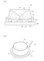
- FIG. 1 is a lateral cross-sectional view of a light-emitting unit according to an exemplary embodiment of the invention in which the light-emitting unit is cut along a direction of an optical axis.
- a light-emitting unit includes a light-emitting element 110, a luminous flux control member 120, and a drive substrate 200.
- the light-emitting element 110 is disposed on the drive substrate 200 and is electrically connected to a circuit pattern formed on the drive substrate 200.
- the light-emitting element 110 may be a chip or a package.
- the light-emitting element 110 may employ various types of optical elements that convert an electrical signal to an optical signal.
- the light-emitting element 110 is a light-emitting diode functioning as a dot light source.
- the luminous flux control member 120 functions to improve illuminance uniformity of the light-emitting unit by refracting light incident from the light-emitting element 110 as a light source to control an optical path.
- the luminous flux control member 120 may include optical lenses.
- the luminous flux control member 120 may be disposed to cover at least a part of the outer surface of the light-emitting element 110.
- the luminous flux control member 120 is embodied in a shape in which a first optical surface S2 is recessed toward the light-emitting element 110.
- the luminous flux control member 120 may be separated from the light-emitting element 110 as illustrated in FIG. 1 .
- light emitted from the light-emitting element 110 maybe incident on the luminous flux control member 120 through a surface of the luminous flux control member 120 which is disposed to face the light-emitting element 110. That is, an incident surface is formed by an outer surface of the luminous flux control member 120.
- the luminous flux control member 120 may be embodied in an integrated optical lens (IOL) type, that is, a light-emitting element integrated type, in which at least a part of the light-emitting element 110 is accommodated in the luminous flux control member 120.
- IOL integrated optical lens
- light emitted from the light-emitting element 110 may be incident on the luminous flux control member 120 through an interface between the luminous flux control member 120 and the outer surface of the light-emitting element 110.
- the interface between the luminous flux control member 120 and the outer surface of the light-emitting element 110 functions as an incident surface on which light is incident from the light-emitting element 110.
- the luminous flux control member 120 includes an incident surface S1 on which light from the light-emitting element 110 is incident, a first optical surface S2 that is separated from the incident surface S1 in a direction of an optical axis (OA), and a second optical surface S3 that extends from the first optical surface S2 toward the incident surface S 1.
- incident surface S1 on which light from the light-emitting element 110 is incident
- first optical surface S2 that is separated from the incident surface S1 in a direction of an optical axis (OA)
- OA optical axis
- the optical axis (OA) may be a virtual line indicating a traveling direction of light at the center of a stereoscopic luminous flux emitted from the light-emitting element 110 or a virtual line connecting the center of the incident surface S1 to the center of the first optical surface S2. Accordingly, in the luminous flux control member 120, the center of the incident surface S1 formed on the bottom and the center of the first optical surface S2 formed on the top may be located on the optical axis (OA).
- the luminous flux control member 120 may further include a flange 121.
- the flange 121 is an edge that protrudes from the entire periphery of the luminous flux control member 120 for the purpose of reinforcing the luminous flux control member 120.
- the flange 121 includes a top surface 121a connected to the second optical surface S3 and a bottom surface 121b connected to the incident surface S1.
- the luminous flux control member 120 may further include a plurality of support portions 122 that protrude from the bottom surface of the flange 121 or the incident surface S1 in the direction of the optical axis (OA).
- a filler 130 may be disposed to surround the light-emitting element 110 and the luminous flux control member 120 maybe disposed on the filler 130. That is, the filler may fill a space between the incident surface S1 of the luminous flux control member 120 and the light-emitting element 110. Light emitted from the light-emitting element 110 passes through the filler 130 and is incident on the luminous flux control member 120 through the incident surface S1 of the luminous flux control member 120.
- FIG. 1 illustrates an example in which one light-emitting element 110 and one luminous flux control member 120 are disposed on one drive substrate 200, but the invention is not limited to this example.
- a plurality of light-emitting elements 110 may be disposed on one drive substrate 200.
- a plurality of luminous flux control members 120 may be disposed to correspond to one light-emitting element 110.
- FIGS. 2 to 6 illustrate an example in which the luminous flux control member 120 includes the flange 121 and the support portions 122, but the invention is not limited to this example.
- the luminous flux control member 120 may not include the flange 121 or the support portions 122.
- FIG. 2 is a perspective view illustrating a luminous flux control member according to an exemplary embodiment of the invention
- FIGS. 3 to 5 are a top view, a bottom view, and a side view of the luminous flux control member according to the exemplary embodiment of the invention, respectively.
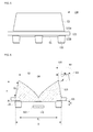
- FIG. 6 is a lateral cross-sectional view of the luminous flux control member according to the exemplary embodiment of the invention in which the luminous flux control member is cut along the direction of the optical axis.
- FIG. 7 is a diagram illustrating a phenomenon of light splash occurring due to deformation of an edge of the luminous flux control member.
- FIG. 8 illustrates optical characteristics of the luminous flux control member depending on the width of a connection portion that is formed in the first optical surface.
- the luminous flux control member 120 includes an incident surface S1 which is disposed to face the light-emitting element 110 and on which light emitted from the light-emitting element 110 is incident, a first optical surface S2 that is separated from the incident surface S1 in the direction of the optical axis (OA) and is recessed toward the incident surface S1, and a second optical surface S3 that extends from the first optical surface S2 to the incident surface S1.
- the incident surface S1 is formed on the surface of the luminous flux control member 120 facing the light-emitting element 110.
- FIGS. 2 to 6 illustrate an example in which the light-emitting element 110 is located outside the luminous flux control member 120, but the luminous flux control member 120 may be an IOL type in which the light-emitting element 110 is accommodated therein.
- the incident surface S1 of the luminous flux control member 120 is not the outer surface of the luminous flux control member 120, but an inner surface corresponding to the interface between the luminous flux control member 120 and the light-emitting element 110.
- the incident surface S1 may include a flat surface.
- the incident surface S 1 may include a spherical surface or an aspherical surface.
- a cross-section of the incident surface S1 taken along the direction of the optical axis (OA) may include a flat section.
- a cross-section of the incident surface S1 taken along the direction of the optical axis (OA) may include a curved section.
- the cross-section of the incident surface S1 taken along the direction of the optical axis (OA) may include a curved section connecting the center to the edge.
- the incident surface S1 may include a concave portion that is recessed toward the first optical surface S2. In this case, a part or all of the light-emitting element 110 maybe accommodated in the concave portion of the incident surface S1.
- the incident surface S1 may include a protruding portion that protrudes toward the light-emitting element 110.
- the incident surface S1 includes a concave portion that is recessed toward the first optical surface S2 at the center thereof and a protruding portion that protrudes toward the light-emitting element 110 on the surface connecting the center to the edge.
- the incident surface S1 may have a rotationally-symmetric structure with respect to the optical axis (OA).
- the incident surface S1 may be formed in a circular shape as illustrated in FIG. 4 .
- the incident surface S1 may have a rotationally-asymmetric structure with respect to the optical axis (OA).
- the first optical surface S2 is separated from the incident surface S1 in the direction of the optical axis (OA) and may include a concave portion S23 that is recessed toward the incident surface S1 and a connection portion S21 extending from the edge of the concave portion S23
- a center S22 of the concave portion S23 is recessed toward the incident surface and the center S22 of the concave portion S23 corresponds to the center of the first optical surface S2.
- the center S22 of the concave portion S23 may be located on the optical axis OA.
- the center S22 of the concave portion S23 may be recessed deeper toward the incident surface S 1.
- the center S22 of the concave portion S23 is recessed toward the incident surface S1 by half the height H of the luminous flux control member 120 or greater, excluding the support portion 122.
- the concave portion S23 may connect the center S22 to the edge with a curve. That is, the concave portion S23 may connect the center S22 of the concave portion S23 to the connection portion S21 on the periphery of the concave portion S23 in a curved shape.
- the shape of the curve connecting the center S22 of the concave portion S23 to the connection portion S21 may be a curved shape convex to the optical axis OA.
- connection portion S21 extends from the edge of the concave portion S23 in the peripheral direction (direction perpendicular to the optical axis) of the second optical surface S3 to form a peripheral portion of the first optical surface S2.
- connection portion S21 functions to connect the concave portion S23 to the second optical surface S3 and to protect the concave portion S23 from a deformation such as a recess.
- the connection portion S21 has a ring shape with a predetermined width W1
- the inner peripheral surface S211 of the ring is connected to the edge of the concave portion S23
- the outer peripheral surface S212 of the ring is connected to the second optical surface S3.
- the concave portion S23 and the second optical surface S3 form a sharp edge.
- a deformation such as a recess may occur in the edge formed by the first optical surface S2 and the second optical surface S3 due to an external environment.
- the deformation of the edge formed by the first optical surface S2 and the second optical surface S3 may serve as a factor for causing the phenomenon of light splash in a light-emitting unit.
- FIGS. 7A and 7B when deformation by recess occurs in the edge of the luminous flux control member 120 as illustrated in FIG. 7A , an area 5 in which illuminance is abnormally high in a region separate from the center of an illuminance surface of the luminous flux control member 120 due to the phenomenon of light splash is generated as illustrated in FIG. 7B .
- the luminous flux control member 120 unsusceptible to recessing is provided by disposing the connection portion S21 as an allowance portion between the concave portion S23 and the second optical surface S3.
- the connection portion S21 functions as a protective section for protecting the concave portion S23, which is an important portion for determining the optical characteristics of the luminous flux control member 120, from recessing or the like and forms an edge less susceptible to recessing than the concave portion S23.
- connection portion S21 when the width W1 of the connection portion S21 is excessively large, the illuminance distribution of the luminous flux control member 120 maybe adversely influenced. Accordingly, it is necessary to limit the width of the connection portion S21.
- the illuminance distribution of the luminous flux control member 120 is insignificantly influenced when the width W1 of the connection portion S21 is equal to or less than 50 mm, but the illuminance distribution of the luminous flux control member 120 is changed when the width W1 of the connection portion S21 is greater than 70 mm.
- the width W1 of the connection portion S21 may vary depending on the size of the luminous flux control member 120 and products to which the luminous flux control member 120 is applied. For example, when the luminous flux control member 120 is applied to a 42" backlight unit and the width W1 of the connection portion S21 is equal to or less than 100 mm, the illuminance distribution of the luminous flux control member 120 is insignificantly influenced.
- connection portion S21 preferably ranges from 1 mm to 100 mm.
- connection portion S21 may connect the connection portion S23 to the second optical surface S3 in a linear shape. That is, the connection portion S21 may include a flat surface.
- connection portion S21 When the connection portion S21 is designed as a flat surface connecting the concave portion S23 to the second optical surface S3, the connection portion S21 may be deformed into a curved surface depending on the shrinkage rate of the luminous flux control member 120 during the course of manufacturing.
- connection portion S21 may include a curved section connecting the concave portion S23 to the second optical surface S3. That is, the connection portion S21 may include a curved surface.
- the connection portion S21 may include both a flat section and a curve section that connect the concave portion S23 to the second optical surface S3. That is, the connection portion S21 may include both a curved surface and a flat surface.
- connection portion S21 When the connection portion S21 includes a curved surface, the connection portion S21 may include a protruding portion that protrudes to the outside of the luminous flux control member 120 and has a peak and a valley.
- the radius of curvature R of the curved section forming the connection portion S21 is equal to or greater than 1/2 W1 (the width of the connection portion S21) and the radius of curvature R of the flat section constituting the connection portion S21 maybe infinite.
- the first optical surface S2 may have a rotationally-symmetric structure with respect to the optical axis (OA).
- the incident surface S1 may have a circular shape as illustrated in FIG. 3 .
- the first optical surface S2 may have a diameter smaller than the maximum diameter of the second optical surface S3.
- the second optical surface S3 forms an outer side surface of the luminous flux control member 120.
- the second optical surface S3 may be inclined with respect to the optical axis (OA).
- the second optical surface S3 may extend from the connection portion S21 of the first optical surface S2 to a lateral-bottom side.
- the second optical surface S3 maybe bent from the connection portion S21 of the first optical surface S2. That is, the second optical surface S3 and the connection portion S21 may form an edge.
- the bending means a shape in which two surfaces are connected to form an edge.
- the two surfaces are connected to form an edge with a radius of curvature of about 0.2 mm or less, it can be said that the two surfaces are bent.
- the second optical surface S3 may be formed as a surface connecting the first optical surface S2 to the incident surface S1.
- the second optical surface S3 may include a flat section or a curved section connecting the first optical surface S2 to the incident surface S 1.
- the second optical surface S3 may be formed as a surface connecting the first optical surface S2 to the flange S21.
- the second optical surface S3 may include a flat section or a curved section connecting the first optical surface S2 to the flange 121.
- the second optical surface S3 may have a rotationally-symmetric structure with respect to the optical axis (OA).
- the second optical surface S3 has a circular cross-section perpendicular to the optical axis (OA) as illustrated in FIG. 3 .
- the second optical surface S3 may be designed so that the maximum diameter thereof is greater than the diameter of the first optical surface S2 and the minimum diameter S3 is equal to the diameter of the first optical surface S2.
- the second optical surface S3 maybe disposed as a curved surface in which the closer it becomes to the first optical surface S2, the closer it becomes to the optical axis (OA). That is, the diameter of the second optical surface S3 becomes larger as it becomes closer to the incident surface S1 and becomes smaller as it becomes closer to the first optical surface S2.
- the flange 121 is formed to protrude from the entire periphery of the luminous flux control member 120 and is disposed between the second optical surface S3 and the incident surface S1. That is, the flange 121 connects the second optical surface S3 to the incident surface S 1.
- the flange 121 has a diameter greater than the maximum diameter of the second optical surface S3 as illustrated in FIG. 3 and has an inner surface in contact with the periphery of the second optical surface S3 as illustrated in FIG. 4 .
- the support portion 122 is a support means for separating the incident surface S1 of the luminous flux control member 120 from the light-emitting element 110 and protrudes from the flange 121 or the incident surface S1 in the direction of the optical axis (OA).
- three support portions 122 are formed to protrude from the bottom surface of the flange 121.
- the support portion 122 has a length greater than the height of the light-emitting element 110 so as to separate the incident surface S1 of the luminous flux control member 120 from the light-emitting element 110 by a predetermined gap.
- the incident surface S1 and the light-emitting element 110 are separated from each other by a predetermined gap so as to guarantee illuminance uniformity.
- the gap G between the incident surface S1 and the light-emitting element 110 ranges from 0.1 mm to 2 mm.
- the ratio (D/H) of the diameter (D) to the height (H) ranges from 0.5 to 5.
- the ratio (D/H) of the diameter (D) to the height (H) is 2.5.
- the diameter (D) maybe the maximum diameter of the part of the luminous flux control member 120, excluding the flange, that is, the maximum diameter of the second optical surface S3.
- the curved section may satisfy a spline curve which is a nonlinear numerical analysis technique.
- the spline curve as a function for forming a smooth curve with a small number of control points, may define an interpolation curve passing through selected control points and an approximate curve of a line connecting the selected control points.
- a B-spline curve, a Bezier curve, a non-uniform rational B-spline (NURBS) curve, a cubic spline curve, and the like can be used as the spline curve.
- the curved section constituting the cross-section of each surface can be expressed by a Bezier curve equation.
- the Bezier curve equation is a function for acquiring various free curves by movement of a start point as a first control point, an end point as a final control point, and internal control points located therebetween and may be expressed by Expression 1.
- B(u) represents a continuous function for calculating a curve acquired by N control points located at different positions
- N represents a parameter for determining the order of the Bezier curve equation
- P k represents the coordinate of the k-th control point and includes N+1 control points.
- u is a real number in the range of 0 to 1 and represents a curved section in which the control points are segmented in the range of 0 to 1.
- B(u) is a blending function which is a function for generating a curve by blending the control points.
- the Bezier curve may have a varying shape depending on the positions of the control points.
- the luminous flux control member 120 having the aforementioned structure may cause a part of light incident from the light-emitting element 110 to travel through a first optical path in which light is totally reflected onto the second optical surface S3 through the use of the first optical surface S2, is reflected through the use of the second optical surface S3, and is then emitted therefrom and a second optical path in which light is totally reflected onto the first optical surface S2 through the use of the second optical surface S3, is refracted through the use of the first optical surface S2, and is emitted to the outside.
- FIG. 9 is a diagram illustrating optical characteristics of the luminous flux control member 120 according to the exemplary embodiment of the invention.
- the incident surface S1 of the luminous flux control member 120 functions to refract light incident from the light-emitting element 110 and to cause the refracted light to travel onto the first optical surface S2 or the second optical surface S3.
- the incident surface S1 When light emitted from the light-emitting element 110 is incident, the incident surface S1 refracts the incident light depending on the incidence angle thereof to travel to the inside of the luminous flux control member 120.
- the first optical surface S2 When light passing through the inside of the luminous flux control member 120 is incident, the first optical surface S2 refracts a part of the incident light to be emitted from the luminous flux control member 120 and totally reflects the remaining incident light to be incident on the second optical surface S3.
- the second optical surface S3 When light passing through the inside of the luminous flux control member 120 is incident, the second optical surface S3 refracts a part of the incident light to be emitted from the luminous flux control member 120 and totally reflects the remaining incident light to be incident on the first optical surface S2.
- the first optical surface S2 When the light totally reflected by the second optical surface S3 is incident, the first optical surface S2 refracts the incident light to be emitted from the luminous flux control member 120.
- the second optical surface S3 When light totally reflected by the first optical surface S2 is incident, the second optical surface S3 refracts the incident light to be emitted from the luminous flux control member 120.
- the traveling angle of light is defined by a left-hand rule with respect to the Y axis parallel to the optical axis (OA).
- the clockwise direction about the Y axis is defined to be positive (+) and the counterclockwise direction is defined to be negative (-).
- angles at which light emitted from the light-emitting element 110 is incident on the incident surface S1 are defined as ⁇ 1 and ⁇ 2, and angles at which the light refracted by the incident surface S1 travels to the first optical surface S2 and the second optical surface S3 are defined as ⁇ 3 and ⁇ 4, respectively.
- Angles at which the light reflected by the first optical surface S2 and the second optical surface S3 is reflected to be emitted to the outside by the second optical surface S3 and the first optical surface S2 are defined as ⁇ 5 and ⁇ 6, respectively
- the first optical surface S2 functions as a totally-reflecting surface that totally reflects a part of light incident through the incident surface S1 to the second optical surface S3.
- a part of light refracted by the incident surface S1 is totally reflected by the first optical surface S2, is incident on the second optical surface S3, is refracted to be emitted from the luminous flux control member 120 by the second optical surface S3.
- First light L1 illustrated FIG. 9 will be described below as an example.
- the first light L1 with an incidence angle ⁇ 1 of light incident on the luminous flux control member 120 traveling from the light-emitting element 110 is refracted by the incident surface S1 and is changed to a traveling angle ⁇ 3.
- the first light L1 traveling at the angle ⁇ 3 is incident on the first optical surface S2 and is reflected by the first optical surface S2.
- the first light reflected by the first optical surface S2 is incident on the second optical surface S3 and is refracted to be emitted to the outside at an angle ⁇ 5 by the second optical surface S3.
- the first light L1 In the traveling path of the first light L1, the first light L1 is incident at a positive angle ⁇ 1, is reflected by the first optical surface S2, and is finally refracted at a positive angle ⁇ 5 to be emitted to the outside through the use of the second optical surface S3. Therefore, both the incidence angle ⁇ 1 and the emission angle ⁇ 5 are positive and satisfy " ⁇ 5/ ⁇ 1>0".
- the first optical surface S2 functions as a refracting surface that refracts the light totally reflected by the second optical surface S3 to be emitted from the luminous flux control member 120. That is, a part of light refracted by the incident surface S1 is reflected by the second optical surface S3 and, is then incident on the first optical surface S2. The first optical surface S2 refracts the incident light to be emitted from the luminous flux control member 120.
- Second light L2 illustrated FIG. 9 will be described below as an example.
- the second light L2 with an incidence angle ⁇ 2 of light incident on the luminous flux control member 120 traveling from the light-emitting element 110 is refracted by the incident surface S1 and is changed to a traveling angle ⁇ 4.
- the second light L2 traveling at the angle ⁇ 4 is incident on the second optical surface S3 and is totally reflected by the second optical surface S3.
- the second light totally reflected by the second optical surface S3 is incident on the first optical surface S2 and is refracted to be emitted to the outside at an angle ⁇ 6 by the first optical surface S2.
- the second light L2 In the traveling path of the second light L2, the second light L2 is incident at a positive angle ⁇ 2, is reflected by the second optical surface S3, and is finally refracted at a negative angle ⁇ 6 to be emitted to the outside through the use of the first optical surface S2. Therefore, one of the incidence angle and the emission angle is negative and the other is positive, whereby " ⁇ 6/ ⁇ 2 ⁇ 0" is satisfied.
- the luminous flux control member 120 can cause a part, which satisfies a predetermined condition, of incident light to travel through the first optical path or the second optical path.
- the luminous flux control member 120 can cause a part, which travels through the incident surface S1 and has a traveling angle within ⁇ 60 degrees, of the incident light to travel through the first optical path or the second optical path.
- the incidence angle range of light which travels through the incident surface S1 and which has a traveling angle within ⁇ 60 degrees may be within ⁇ 85 degrees. That is, the incident surface S1 refracts a part, which has an incidence angle within ⁇ 85 degrees, of the incident light to travel at an angle within ⁇ 60 degrees.
- the light which passes through the incident surface S1 and which has a traveling angle within ⁇ 60 degrees is incident on the first optical surface S2 or the second optical surface S3, travels through the first optical path or the second optical path, and is emitted from the luminous flux control member 120.
- the incident surface S1 refracts a part, which satisfies a predetermined condition, of the incident light to be incident on the first optical surface S2 and refracts the remaining light to be incident on the second optical surface S3.
- the incident surface S1 refracts a part, which has an incidence angle within ⁇ 80 degrees, of the incident light to travel to the first optical surface S2 and refracts the remaining incident light to travel to the second optical surface S3.
- a part of the light, which passes through the incident surface S1 and is incident on the first optical surface S2 is reflected onto second optical surface S3 and the remaining incident light is refracted and emitted to the outside.
- FIG. 9 illustrates the optical path in the right section when the luminous flux control member 120 is divided into two sections with respect to the optical axis (OA).
- the first light L1 travels through the first optical path and the second light L2 travels through the second optical path. Then, the first light L1 corresponding to light traveling when the first optical surface S2 functions as a reflecting surface travels and is emitted to the right side with respect to the optical axis (OA). On the contrary, the second light L2 corresponding to light traveling when the second optical surface S3 functions as a reflecting surface travels and is emitted to the left side with respect to the optical axis.
- the luminous flux control member 120 needs to be designed so that K is within a range of 0.25 to 2.5 in order to improve illuminance uniformity.
- the luminous flux control member according to the exemplary embodiment of the invention can be applied to an illumination unit, a backlight unit of a liquid crystal display, or the like.
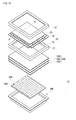
- FIG. 10 is an exploded perspective view of a liquid crystal display according to an exemplary embodiment of the invention to which the luminous flux control member described above with reference to FIGS. 1 to 9 is applied.
- FIG. 11 is a cross-sectional view of a backlight unit of the liquid crystal display according to the exemplary embodiment of the invention taken along line A-A' of FIG. 10 .
- the liquid crystal display includes a backlight unit 10 and a liquid crystal panel 20.
- the liquid crystal panel 20 is a display component of the liquid crystal display and includes a thin film transistor (TFT) substrate, a color filter substrate, and a liquid crystal layer interposed between two substrates.
- TFT substrate includes a plurality of gate lines, a plurality of data lines intersecting the plurality of gate lines, and thin film transistors (TFT) formed at intersections of the gate lines and the data lines.
- a driving circuit unit 30 may be connected to one side of the liquid crystal panel 20.
- the driving circuit unit 30 includes a printed circuit board (PCB) 31 that supplies scanning signals to the gate lines of the TFT substrate and a printed circuit board 32 that supplies data signals to the data lines.
- PCB printed circuit board
- the driving circuit unit 30 is electrically connected to the liquid crystal panel 20 in a chip-on-film (COF) manner, a tape carrier package (TCP) manner, or the like.
- COF chip-on-film
- TCP tape carrier package
- the liquid crystal display may further include a panel guide 21 that supports the liquid crystal panel 20 and an upper case 22 coupled to the panel guide 21 so as to surround the edge of the liquid crystal panel 20.
- the backlight unit 10 is coupled to the liquid crystal panel 20 in a direct type and includes a bottom cover 300, a drive substrate 200, a plurality of light source units 100, and a plurality of optical sheets 400.
- the bottom cover 300 is formed of a metal or the like and has a box shape of which the top is opened.
- the bottom cover 300 may be formed by bending or curving a metal plate or the like.
- the drive substrate 200 is accommodated in a space of the bottom cover 300 formed by bending or curving.
- the bottom cover 300 functions to support the optical sheets 400 and the liquid crystal panel 20.
- the drive substrate 200 has a plate shape and a reflecting layer may be formed on the drive substrate 200.
- the reflecting layer functions to reflect light emitted from the light-emitting element 110 to improve performance of the backlight unit 10.
- the plurality of light source units 100 may be mounted on the drive substrate 200.
- Each light source unit 100 may include a light-emitting element 110 and a luminous flux control member 120 disposed to cover the light-emitting element 110.
- FIGS. 9 and 10 illustrate an example in which the light-emitting element 110 is a light-emitting diode.
- the light-emitting diodes 110 are disposed on the drive substrate 200 and are electrically connected to the drive substrate 200.
- the light-emitting diodes 110 emit light in response to a driving signal supplied from the drive substrate 200.
- Each light-emitting diode 110 functions as a dot light source and an array of the light-emitting diodes 110 arranged at predetermined intervals on the drive substrate 200 may form a surface light source.
- Each light-emitting diode 110 may be disposed in the form of a light-emitting diode package including a light-emitting diode chip. Each light-emitting diode 110 may emit white light or may selectively emit blue light, green light, and red light.
- the luminous flux control member 120 When light emitted from the light-emitting diode 110 is incident, the luminous flux control member 120 functions to control a luminous flux to improve illuminance uniformity.
- the luminous flux control member 120 may be provided separate from the light-emitting diode 110.
- the luminous flux control member 120 may be provided as an IOL type in which the light-emitting diode 110 is accommodated therein.
- FIGS. 10 and 11 illustrate an example in which the luminous flux control members 120 are separated from each other and are arranged at predetermined intervals, but the invention is not limited to this example.
- the luminous flux control members may be embodied in the form in which the plurality of luminous flux control members 120 arranged at predetermined intervals corresponding to the light-emitting diodes 110 are incorporated into one structure.
- the optical sheets include a diffusing sheet 410, a polarizing sheet 420, and a prism sheet 430 and may be used to improve characteristics of light passing through the optical sheets 400.
- the diffusing sheet 410 causes light incident from the light source unit 100 to travel onto the front surface of the liquid crystal panel 20, diffuses the light so as to have a uniform distribution in a wide range, and applies the diffused light to the liquid crystal panel 20.
- the polarizing sheet 420 functions to polarize obliquely-incident of light incident on the polarizing sheet 420 so as to be emitted perpendicularly. At least one polarizing sheet 420 may be disposed under the liquid crystal panel 20 in order to change light emitting from the diffusing sheet 410 to be perpendicular.
- the prism sheet 430 transmits light parallel to a transmission axis thereof and reflects light perpendicular to the transmission axis.
- the backlight unit 10 can apply light having improved illuminance uniformity to the liquid crystal panel 20 and thus the liquid crystal display can realize improved image quality with improved illuminance uniformity.
Landscapes
- Physics & Mathematics (AREA)
- General Physics & Mathematics (AREA)
- Optics & Photonics (AREA)
- Nonlinear Science (AREA)
- Mathematical Physics (AREA)
- Chemical & Material Sciences (AREA)
- Crystallography & Structural Chemistry (AREA)
- Engineering & Computer Science (AREA)
- General Engineering & Computer Science (AREA)
- Planar Illumination Modules (AREA)
Applications Claiming Priority (1)
| Application Number | Priority Date | Filing Date | Title |
|---|---|---|---|
| KR1020140006274A KR102174249B1 (ko) | 2014-01-17 | 2014-01-17 | 광속제어부재, 발광장치 및 표시장치 |
Publications (2)
| Publication Number | Publication Date |
|---|---|
| EP2896984A1 true EP2896984A1 (de) | 2015-07-22 |
| EP2896984B1 EP2896984B1 (de) | 2020-07-29 |
Family
ID=52595031
Family Applications (1)
| Application Number | Title | Priority Date | Filing Date |
|---|---|---|---|
| EP15151361.1A Active EP2896984B1 (de) | 2014-01-17 | 2015-01-16 | Element zur Lichtstromsteuerung, lichtemittierende Einheit und Anzeigevorrichtung |
Country Status (4)
| Country | Link |
|---|---|
| US (1) | US9703130B2 (de) |
| EP (1) | EP2896984B1 (de) |
| KR (1) | KR102174249B1 (de) |
| CN (1) | CN104791709A (de) |
Families Citing this family (3)
| Publication number | Priority date | Publication date | Assignee | Title |
|---|---|---|---|---|
| JP6425415B2 (ja) * | 2014-05-02 | 2018-11-21 | 株式会社エンプラス | 光束制御部材、発光装置および照明装置 |
| JP6507035B2 (ja) * | 2015-06-03 | 2019-04-24 | 株式会社エンプラス | 光束制御部材、発光装置および照明装置 |
| JP6869667B2 (ja) * | 2016-08-31 | 2021-05-12 | 三菱電機株式会社 | 面光源装置および液晶表示装置 |
Citations (4)
| Publication number | Priority date | Publication date | Assignee | Title |
|---|---|---|---|---|
| US20090032827A1 (en) * | 2007-07-30 | 2009-02-05 | Philips Lumileds Lighting Company, Llc | Concave Wide Emitting Lens for LED Useful for Backlighting |
| US20120032202A1 (en) * | 2009-04-14 | 2012-02-09 | Sharp Kabushiki Kaisha | Planar light source device and display device provided with the planar light source device |
| US20120086875A1 (en) * | 2009-06-30 | 2012-04-12 | Sharp Kabushiki Kaisha | Lighting device, display device and television receiver |
| US20130088857A1 (en) * | 2011-10-11 | 2013-04-11 | Kyungjoon LEE | Optical assembly, backlight unit having the same, and display apparatus thereof |
Family Cites Families (15)
| Publication number | Priority date | Publication date | Assignee | Title |
|---|---|---|---|---|
| JPWO2003100367A1 (ja) * | 2002-05-08 | 2005-09-22 | コナミ株式会社 | 模型用受光装置、模型、及び模型用信号光検出方法 |
| KR101112552B1 (ko) * | 2005-03-08 | 2012-02-15 | 삼성전자주식회사 | 발광 다이오드용 렌즈, 발광 다이오드, 이를 포함하는 백라이트 어셈블리 및 액정 표시 장치 |
| KR20070013469A (ko) * | 2005-07-26 | 2007-01-31 | 삼성전자주식회사 | 광학렌즈 및 광학 패키지와, 이를 갖는 백라이트 어셈블리및 표시장치 |
| JP4993616B2 (ja) * | 2008-03-05 | 2012-08-08 | 株式会社エンプラス | 発光装置、面光源装置、及び表示装置 |
| KR100990426B1 (ko) | 2008-09-04 | 2010-10-29 | 주식회사 헤파스 | 빛의 후면 확산방출 수단을 갖는 엘이디 광확산 렌즈 |
| KR101028304B1 (ko) * | 2009-10-15 | 2011-04-11 | 엘지이노텍 주식회사 | 발광 장치 |
| KR100986468B1 (ko) * | 2009-11-19 | 2010-10-08 | 엘지이노텍 주식회사 | 렌즈 및 렌즈를 갖는 발광 장치 |
| JP2011204657A (ja) * | 2010-03-26 | 2011-10-13 | Enplas Corp | 光束制御部材およびこれを用いた照明装置 |
| TWI561770B (en) * | 2010-04-30 | 2016-12-11 | Samsung Electronics Co Ltd | Light emitting device package, light source module, backlight unit, display apparatus, television set, and illumination apparatus |
| JP5896108B2 (ja) * | 2011-09-09 | 2016-03-30 | 株式会社エンプラス | 光束制御部材およびこれを備えた発光装置 |
| TWI606618B (zh) * | 2012-01-03 | 2017-11-21 | Lg伊諾特股份有限公司 | 發光裝置 |
| JP5839686B2 (ja) * | 2012-01-27 | 2016-01-06 | 株式会社エンプラス | 光束制御部材および発光装置 |
| JP6085105B2 (ja) * | 2012-06-22 | 2017-02-22 | 株式会社エンプラス | 光束制御部材、発光装置、照明装置および表示装置 |
| KR102023540B1 (ko) * | 2012-08-08 | 2019-09-24 | 엘지이노텍 주식회사 | 광속 제어 부재, 발광 장치 및 표시 장치 |
| JP6111110B2 (ja) * | 2012-08-27 | 2017-04-05 | 株式会社エンプラス | 光束制御部材、発光装置、面光源装置および表示装置 |
-
2014
- 2014-01-17 KR KR1020140006274A patent/KR102174249B1/ko not_active Expired - Fee Related
-
2015
- 2015-01-16 US US14/598,310 patent/US9703130B2/en active Active
- 2015-01-16 EP EP15151361.1A patent/EP2896984B1/de active Active
- 2015-01-19 CN CN201510025511.3A patent/CN104791709A/zh active Pending
Patent Citations (4)
| Publication number | Priority date | Publication date | Assignee | Title |
|---|---|---|---|---|
| US20090032827A1 (en) * | 2007-07-30 | 2009-02-05 | Philips Lumileds Lighting Company, Llc | Concave Wide Emitting Lens for LED Useful for Backlighting |
| US20120032202A1 (en) * | 2009-04-14 | 2012-02-09 | Sharp Kabushiki Kaisha | Planar light source device and display device provided with the planar light source device |
| US20120086875A1 (en) * | 2009-06-30 | 2012-04-12 | Sharp Kabushiki Kaisha | Lighting device, display device and television receiver |
| US20130088857A1 (en) * | 2011-10-11 | 2013-04-11 | Kyungjoon LEE | Optical assembly, backlight unit having the same, and display apparatus thereof |
Also Published As
| Publication number | Publication date |
|---|---|
| US20150301379A1 (en) | 2015-10-22 |
| CN104791709A (zh) | 2015-07-22 |
| EP2896984B1 (de) | 2020-07-29 |
| KR20150086102A (ko) | 2015-07-27 |
| KR102174249B1 (ko) | 2020-11-04 |
| US9703130B2 (en) | 2017-07-11 |
Similar Documents
| Publication | Publication Date | Title |
|---|---|---|
| US8210730B2 (en) | Surface light source device | |
| US7357557B2 (en) | Light guide plate | |
| JP4959971B2 (ja) | 光学パッケージ、光学レンズ、これを有するバックライトアセンブリ、及び表示装置 | |
| US20100142225A1 (en) | Illuminating device and display device having the same | |
| US9690034B2 (en) | Illumination device and display device | |
| US20230077729A1 (en) | Optical structure comprising a concave-and-convex-shaped interface having a flat portion between a high refractive-index layer and a low refractive-index layer and display device | |
| US20130194823A1 (en) | Backlight unit | |
| US9310546B2 (en) | Backlight unit and display device having the same | |
| US20200159071A1 (en) | Back light unit and display device having the same | |
| EP2821836A1 (de) | Optische Linse, lichtemittierende Vorrichtung und Anzeige | |
| US20090167987A1 (en) | Light Guide Plate, and Backlight Assembly and Liquid Crystal Display Having the Same | |
| TWI578068B (zh) | 直下式導光結構、導光板及背光模組 | |
| CN203585839U (zh) | 背光源单元和液晶显示装置 | |
| EP2555026A1 (de) | Anzeigevorrichtung | |
| US9091798B2 (en) | Display apparatus and backlight assembly | |
| US9709244B2 (en) | Light-source module | |
| EP2896984B1 (de) | Element zur Lichtstromsteuerung, lichtemittierende Einheit und Anzeigevorrichtung | |
| EP2881655A1 (de) | Optisches Element zur Steuerung des Lichtstroms, lichtemittierende Vorrichtung und Anzeigevorrichtung | |
| CN101655193A (zh) | 面发光装置和图像显示装置 | |
| JP6311569B2 (ja) | 面光源装置、表示装置、及び電子機器 | |
| EP2754954A1 (de) | Schwarzlichteinheit | |
| EP2881777A1 (de) | Optisches Element und lichtemittierende Vorrichtung damit | |
| TWI704316B (zh) | 照明裝置、顯示裝置及攜帶用電子機器 | |
| US20190391450A1 (en) | Planar lighting device | |
| US7703936B2 (en) | Illumination device, light guide plate, surface light source device and illumination unit |
Legal Events
| Date | Code | Title | Description |
|---|---|---|---|
| PUAI | Public reference made under article 153(3) epc to a published international application that has entered the european phase |
Free format text: ORIGINAL CODE: 0009012 |
|
| 17P | Request for examination filed |
Effective date: 20150116 |
|
| AK | Designated contracting states |
Kind code of ref document: A1 Designated state(s): AL AT BE BG CH CY CZ DE DK EE ES FI FR GB GR HR HU IE IS IT LI LT LU LV MC MK MT NL NO PL PT RO RS SE SI SK SM TR |
|
| AX | Request for extension of the european patent |
Extension state: BA ME |
|
| 17P | Request for examination filed |
Effective date: 20160121 |
|
| RBV | Designated contracting states (corrected) |
Designated state(s): AL AT BE BG CH CY CZ DE DK EE ES FI FR GB GR HR HU IE IS IT LI LT LU LV MC MK MT NL NO PL PT RO RS SE SI SK SM TR |
|
| RAP1 | Party data changed (applicant data changed or rights of an application transferred) |
Owner name: LG INNOTEK CO., LTD. |
|
| STAA | Information on the status of an ep patent application or granted ep patent |
Free format text: STATUS: EXAMINATION IS IN PROGRESS |
|
| 17Q | First examination report despatched |
Effective date: 20180709 |
|
| GRAP | Despatch of communication of intention to grant a patent |
Free format text: ORIGINAL CODE: EPIDOSNIGR1 |
|
| STAA | Information on the status of an ep patent application or granted ep patent |
Free format text: STATUS: GRANT OF PATENT IS INTENDED |
|
| INTG | Intention to grant announced |
Effective date: 20200514 |
|
| GRAS | Grant fee paid |
Free format text: ORIGINAL CODE: EPIDOSNIGR3 |
|
| GRAA | (expected) grant |
Free format text: ORIGINAL CODE: 0009210 |
|
| STAA | Information on the status of an ep patent application or granted ep patent |
Free format text: STATUS: THE PATENT HAS BEEN GRANTED |
|
| AK | Designated contracting states |
Kind code of ref document: B1 Designated state(s): AL AT BE BG CH CY CZ DE DK EE ES FI FR GB GR HR HU IE IS IT LI LT LU LV MC MK MT NL NO PL PT RO RS SE SI SK SM TR |
|
| REG | Reference to a national code |
Ref country code: CH Ref legal event code: EP |
|
| REG | Reference to a national code |
Ref country code: AT Ref legal event code: REF Ref document number: 1296465 Country of ref document: AT Kind code of ref document: T Effective date: 20200815 |
|
| REG | Reference to a national code |
Ref country code: IE Ref legal event code: FG4D |
|
| REG | Reference to a national code |
Ref country code: DE Ref legal event code: R096 Ref document number: 602015056389 Country of ref document: DE |
|
| REG | Reference to a national code |
Ref country code: LT Ref legal event code: MG4D |
|
| REG | Reference to a national code |
Ref country code: NL Ref legal event code: MP Effective date: 20200729 |
|
| REG | Reference to a national code |
Ref country code: AT Ref legal event code: MK05 Ref document number: 1296465 Country of ref document: AT Kind code of ref document: T Effective date: 20200729 |
|
| PG25 | Lapsed in a contracting state [announced via postgrant information from national office to epo] |
Ref country code: AT Free format text: LAPSE BECAUSE OF FAILURE TO SUBMIT A TRANSLATION OF THE DESCRIPTION OR TO PAY THE FEE WITHIN THE PRESCRIBED TIME-LIMIT Effective date: 20200729 Ref country code: NO Free format text: LAPSE BECAUSE OF FAILURE TO SUBMIT A TRANSLATION OF THE DESCRIPTION OR TO PAY THE FEE WITHIN THE PRESCRIBED TIME-LIMIT Effective date: 20201029 Ref country code: GR Free format text: LAPSE BECAUSE OF FAILURE TO SUBMIT A TRANSLATION OF THE DESCRIPTION OR TO PAY THE FEE WITHIN THE PRESCRIBED TIME-LIMIT Effective date: 20201030 Ref country code: LT Free format text: LAPSE BECAUSE OF FAILURE TO SUBMIT A TRANSLATION OF THE DESCRIPTION OR TO PAY THE FEE WITHIN THE PRESCRIBED TIME-LIMIT Effective date: 20200729 Ref country code: BG Free format text: LAPSE BECAUSE OF FAILURE TO SUBMIT A TRANSLATION OF THE DESCRIPTION OR TO PAY THE FEE WITHIN THE PRESCRIBED TIME-LIMIT Effective date: 20201029 Ref country code: SE Free format text: LAPSE BECAUSE OF FAILURE TO SUBMIT A TRANSLATION OF THE DESCRIPTION OR TO PAY THE FEE WITHIN THE PRESCRIBED TIME-LIMIT Effective date: 20200729 Ref country code: HR Free format text: LAPSE BECAUSE OF FAILURE TO SUBMIT A TRANSLATION OF THE DESCRIPTION OR TO PAY THE FEE WITHIN THE PRESCRIBED TIME-LIMIT Effective date: 20200729 Ref country code: ES Free format text: LAPSE BECAUSE OF FAILURE TO SUBMIT A TRANSLATION OF THE DESCRIPTION OR TO PAY THE FEE WITHIN THE PRESCRIBED TIME-LIMIT Effective date: 20200729 Ref country code: FI Free format text: LAPSE BECAUSE OF FAILURE TO SUBMIT A TRANSLATION OF THE DESCRIPTION OR TO PAY THE FEE WITHIN THE PRESCRIBED TIME-LIMIT Effective date: 20200729 Ref country code: PT Free format text: LAPSE BECAUSE OF FAILURE TO SUBMIT A TRANSLATION OF THE DESCRIPTION OR TO PAY THE FEE WITHIN THE PRESCRIBED TIME-LIMIT Effective date: 20201130 |
|
| PG25 | Lapsed in a contracting state [announced via postgrant information from national office to epo] |
Ref country code: IS Free format text: LAPSE BECAUSE OF FAILURE TO SUBMIT A TRANSLATION OF THE DESCRIPTION OR TO PAY THE FEE WITHIN THE PRESCRIBED TIME-LIMIT Effective date: 20201129 Ref country code: LV Free format text: LAPSE BECAUSE OF FAILURE TO SUBMIT A TRANSLATION OF THE DESCRIPTION OR TO PAY THE FEE WITHIN THE PRESCRIBED TIME-LIMIT Effective date: 20200729 Ref country code: PL Free format text: LAPSE BECAUSE OF FAILURE TO SUBMIT A TRANSLATION OF THE DESCRIPTION OR TO PAY THE FEE WITHIN THE PRESCRIBED TIME-LIMIT Effective date: 20200729 Ref country code: RS Free format text: LAPSE BECAUSE OF FAILURE TO SUBMIT A TRANSLATION OF THE DESCRIPTION OR TO PAY THE FEE WITHIN THE PRESCRIBED TIME-LIMIT Effective date: 20200729 |
|
| PG25 | Lapsed in a contracting state [announced via postgrant information from national office to epo] |
Ref country code: NL Free format text: LAPSE BECAUSE OF FAILURE TO SUBMIT A TRANSLATION OF THE DESCRIPTION OR TO PAY THE FEE WITHIN THE PRESCRIBED TIME-LIMIT Effective date: 20200729 |
|
| PG25 | Lapsed in a contracting state [announced via postgrant information from national office to epo] |
Ref country code: RO Free format text: LAPSE BECAUSE OF FAILURE TO SUBMIT A TRANSLATION OF THE DESCRIPTION OR TO PAY THE FEE WITHIN THE PRESCRIBED TIME-LIMIT Effective date: 20200729 Ref country code: SM Free format text: LAPSE BECAUSE OF FAILURE TO SUBMIT A TRANSLATION OF THE DESCRIPTION OR TO PAY THE FEE WITHIN THE PRESCRIBED TIME-LIMIT Effective date: 20200729 Ref country code: EE Free format text: LAPSE BECAUSE OF FAILURE TO SUBMIT A TRANSLATION OF THE DESCRIPTION OR TO PAY THE FEE WITHIN THE PRESCRIBED TIME-LIMIT Effective date: 20200729 Ref country code: IT Free format text: LAPSE BECAUSE OF FAILURE TO SUBMIT A TRANSLATION OF THE DESCRIPTION OR TO PAY THE FEE WITHIN THE PRESCRIBED TIME-LIMIT Effective date: 20200729 Ref country code: CZ Free format text: LAPSE BECAUSE OF FAILURE TO SUBMIT A TRANSLATION OF THE DESCRIPTION OR TO PAY THE FEE WITHIN THE PRESCRIBED TIME-LIMIT Effective date: 20200729 Ref country code: DK Free format text: LAPSE BECAUSE OF FAILURE TO SUBMIT A TRANSLATION OF THE DESCRIPTION OR TO PAY THE FEE WITHIN THE PRESCRIBED TIME-LIMIT Effective date: 20200729 |
|
| REG | Reference to a national code |
Ref country code: DE Ref legal event code: R097 Ref document number: 602015056389 Country of ref document: DE |
|
| PG25 | Lapsed in a contracting state [announced via postgrant information from national office to epo] |
Ref country code: AL Free format text: LAPSE BECAUSE OF FAILURE TO SUBMIT A TRANSLATION OF THE DESCRIPTION OR TO PAY THE FEE WITHIN THE PRESCRIBED TIME-LIMIT Effective date: 20200729 |
|
| PLBE | No opposition filed within time limit |
Free format text: ORIGINAL CODE: 0009261 |
|
| STAA | Information on the status of an ep patent application or granted ep patent |
Free format text: STATUS: NO OPPOSITION FILED WITHIN TIME LIMIT |
|
| PG25 | Lapsed in a contracting state [announced via postgrant information from national office to epo] |
Ref country code: SK Free format text: LAPSE BECAUSE OF FAILURE TO SUBMIT A TRANSLATION OF THE DESCRIPTION OR TO PAY THE FEE WITHIN THE PRESCRIBED TIME-LIMIT Effective date: 20200729 |
|
| 26N | No opposition filed |
Effective date: 20210430 |
|
| PG25 | Lapsed in a contracting state [announced via postgrant information from national office to epo] |
Ref country code: MC Free format text: LAPSE BECAUSE OF FAILURE TO SUBMIT A TRANSLATION OF THE DESCRIPTION OR TO PAY THE FEE WITHIN THE PRESCRIBED TIME-LIMIT Effective date: 20200729 Ref country code: SI Free format text: LAPSE BECAUSE OF FAILURE TO SUBMIT A TRANSLATION OF THE DESCRIPTION OR TO PAY THE FEE WITHIN THE PRESCRIBED TIME-LIMIT Effective date: 20200729 |
|
| REG | Reference to a national code |
Ref country code: CH Ref legal event code: PL |
|
| REG | Reference to a national code |
Ref country code: DE Ref legal event code: R081 Ref document number: 602015056389 Country of ref document: DE Owner name: SUZHOU LEKIN SEMICONDUCTOR CO. LTD., TAICANG, CN Free format text: FORMER OWNER: LG INNOTEK CO., LTD., SEOUL, KR |
|
| GBPC | Gb: european patent ceased through non-payment of renewal fee |
Effective date: 20210116 |
|
| PG25 | Lapsed in a contracting state [announced via postgrant information from national office to epo] |
Ref country code: LU Free format text: LAPSE BECAUSE OF NON-PAYMENT OF DUE FEES Effective date: 20210116 |
|
| REG | Reference to a national code |
Ref country code: BE Ref legal event code: MM Effective date: 20210131 |
|
| PG25 | Lapsed in a contracting state [announced via postgrant information from national office to epo] |
Ref country code: FR Free format text: LAPSE BECAUSE OF NON-PAYMENT OF DUE FEES Effective date: 20210131 |
|
| PG25 | Lapsed in a contracting state [announced via postgrant information from national office to epo] |
Ref country code: LI Free format text: LAPSE BECAUSE OF NON-PAYMENT OF DUE FEES Effective date: 20210131 Ref country code: CH Free format text: LAPSE BECAUSE OF NON-PAYMENT OF DUE FEES Effective date: 20210131 Ref country code: GB Free format text: LAPSE BECAUSE OF NON-PAYMENT OF DUE FEES Effective date: 20210116 |
|
| PG25 | Lapsed in a contracting state [announced via postgrant information from national office to epo] |
Ref country code: IE Free format text: LAPSE BECAUSE OF NON-PAYMENT OF DUE FEES Effective date: 20210116 |
|
| PG25 | Lapsed in a contracting state [announced via postgrant information from national office to epo] |
Ref country code: IS Free format text: LAPSE BECAUSE OF FAILURE TO SUBMIT A TRANSLATION OF THE DESCRIPTION OR TO PAY THE FEE WITHIN THE PRESCRIBED TIME-LIMIT Effective date: 20201129 |
|
| PG25 | Lapsed in a contracting state [announced via postgrant information from national office to epo] |
Ref country code: BE Free format text: LAPSE BECAUSE OF NON-PAYMENT OF DUE FEES Effective date: 20210131 |
|
| PG25 | Lapsed in a contracting state [announced via postgrant information from national office to epo] |
Ref country code: HU Free format text: LAPSE BECAUSE OF FAILURE TO SUBMIT A TRANSLATION OF THE DESCRIPTION OR TO PAY THE FEE WITHIN THE PRESCRIBED TIME-LIMIT; INVALID AB INITIO Effective date: 20150116 |
|
| PG25 | Lapsed in a contracting state [announced via postgrant information from national office to epo] |
Ref country code: CY Free format text: LAPSE BECAUSE OF FAILURE TO SUBMIT A TRANSLATION OF THE DESCRIPTION OR TO PAY THE FEE WITHIN THE PRESCRIBED TIME-LIMIT Effective date: 20200729 |
|
| PG25 | Lapsed in a contracting state [announced via postgrant information from national office to epo] |
Ref country code: MK Free format text: LAPSE BECAUSE OF FAILURE TO SUBMIT A TRANSLATION OF THE DESCRIPTION OR TO PAY THE FEE WITHIN THE PRESCRIBED TIME-LIMIT Effective date: 20200729 |
|
| PG25 | Lapsed in a contracting state [announced via postgrant information from national office to epo] |
Ref country code: TR Free format text: LAPSE BECAUSE OF FAILURE TO SUBMIT A TRANSLATION OF THE DESCRIPTION OR TO PAY THE FEE WITHIN THE PRESCRIBED TIME-LIMIT Effective date: 20200729 |
|
| PG25 | Lapsed in a contracting state [announced via postgrant information from national office to epo] |
Ref country code: MT Free format text: LAPSE BECAUSE OF FAILURE TO SUBMIT A TRANSLATION OF THE DESCRIPTION OR TO PAY THE FEE WITHIN THE PRESCRIBED TIME-LIMIT Effective date: 20200729 |
|
| PGFP | Annual fee paid to national office [announced via postgrant information from national office to epo] |
Ref country code: DE Payment date: 20251203 Year of fee payment: 12 |