EP2896944A1 - Temperature sensor and manufacturing method for temperature sensor - Google Patents
Temperature sensor and manufacturing method for temperature sensor Download PDFInfo
- Publication number
- EP2896944A1 EP2896944A1 EP14195651.6A EP14195651A EP2896944A1 EP 2896944 A1 EP2896944 A1 EP 2896944A1 EP 14195651 A EP14195651 A EP 14195651A EP 2896944 A1 EP2896944 A1 EP 2896944A1
- Authority
- EP
- European Patent Office
- Prior art keywords
- side face
- lead wire
- corner
- distal end
- temperature sensor
- Prior art date
- Legal status (The legal status is an assumption and is not a legal conclusion. Google has not performed a legal analysis and makes no representation as to the accuracy of the status listed.)
- Granted
Links
Images





Classifications
-
- H—ELECTRICITY
- H01—ELECTRIC ELEMENTS
- H01C—RESISTORS
- H01C7/00—Non-adjustable resistors formed as one or more layers or coatings; Non-adjustable resistors made from powdered conducting material or powdered semi-conducting material with or without insulating material
- H01C7/008—Thermistors
-
- G—PHYSICS
- G01—MEASURING; TESTING
- G01K—MEASURING TEMPERATURE; MEASURING QUANTITY OF HEAT; THERMALLY-SENSITIVE ELEMENTS NOT OTHERWISE PROVIDED FOR
- G01K7/00—Measuring temperature based on the use of electric or magnetic elements directly sensitive to heat ; Power supply therefor, e.g. using thermoelectric elements
- G01K7/16—Measuring temperature based on the use of electric or magnetic elements directly sensitive to heat ; Power supply therefor, e.g. using thermoelectric elements using resistive elements
-
- G—PHYSICS
- G01—MEASURING; TESTING
- G01K—MEASURING TEMPERATURE; MEASURING QUANTITY OF HEAT; THERMALLY-SENSITIVE ELEMENTS NOT OTHERWISE PROVIDED FOR
- G01K7/00—Measuring temperature based on the use of electric or magnetic elements directly sensitive to heat ; Power supply therefor, e.g. using thermoelectric elements
- G01K7/16—Measuring temperature based on the use of electric or magnetic elements directly sensitive to heat ; Power supply therefor, e.g. using thermoelectric elements using resistive elements
- G01K7/22—Measuring temperature based on the use of electric or magnetic elements directly sensitive to heat ; Power supply therefor, e.g. using thermoelectric elements using resistive elements the element being a non-linear resistance, e.g. thermistor
-
- H—ELECTRICITY
- H01—ELECTRIC ELEMENTS
- H01C—RESISTORS
- H01C1/00—Details
- H01C1/14—Terminals or tapping points specially adapted for resistors; Arrangements of terminals or tapping points on resistors
-
- H—ELECTRICITY
- H01—ELECTRIC ELEMENTS
- H01C—RESISTORS
- H01C17/00—Apparatus or processes specially adapted for manufacturing resistors
-
- Y—GENERAL TAGGING OF NEW TECHNOLOGICAL DEVELOPMENTS; GENERAL TAGGING OF CROSS-SECTIONAL TECHNOLOGIES SPANNING OVER SEVERAL SECTIONS OF THE IPC; TECHNICAL SUBJECTS COVERED BY FORMER USPC CROSS-REFERENCE ART COLLECTIONS [XRACs] AND DIGESTS
- Y10—TECHNICAL SUBJECTS COVERED BY FORMER USPC
- Y10T—TECHNICAL SUBJECTS COVERED BY FORMER US CLASSIFICATION
- Y10T29/00—Metal working
- Y10T29/49—Method of mechanical manufacture
- Y10T29/49002—Electrical device making
- Y10T29/49082—Resistor making
- Y10T29/49085—Thermally variable
Definitions
- the present invention relates to a temperature sensor including a thermistor element, and a manufacturing method for the temperature sensor.
- two lead wires of different lengths are prepared.
- these lead wires are cut at the distal end.
- the cut surfaces of the respective lead wires are inclined inward to each other, with a metal wire being exposed from the cut surface of each of the lead wires.
- a thermistor element is disposed so that the side face of one of the lead wires is attached to the thermistor element in parallel to the longitudinal direction of the thermistor element, and that the distal end of the other lead wire supports a terminal electrode of the thermistor element.
- solder paste is applied to the junction between each of the lead wires and the corresponding terminal electrode. Thereafter, the solder paste is heated with a hot-air heater, causing the solder paste to melt. As a result, the thermistor body is fixed to both of the lead wires.
- an insulating member is applied so as to cover the distal end portions of both of the lead wires and the entire thermistor element, and the insulating member is cured. Thereafter, the terminal end portion of each of the lead wires is immersed in a high temperature solder bath, thereby stripping the insulating coat covering this portion, and solder coating is applied.
- the temperature sensor is completed.
- the thermistor element is merely attached to one of the lead wires, and the terminal electrode of the thermistor element is only supported by the distal end of the other lead wire. Therefore, the thermistor element is held by the two lead wires with a relatively weak force. Consequently, at the time of solder paste application or the like, even application of a small external force causes the thermistor element to dislodge from the lead wires. As a result, the percentage of non-defective products (hereinafter, referred to as "yield rate”) is low with the manufacturing method according to related art.
- a manufacturing method for a temperature sensor including a first disposing step of disposing a first lead wire and a second lead wire side by side, a preparing step of preparing a thermistor element, the thermistor element including a body, and a first outer electrode and a second outer electrode that are provided to the body, the thermistor element having a first side face and a second side face that are opposite to each other, a third side face that is adjacent to the first side face to form a first corner, and a fourth side face that is adjacent to the second side face to form a second corner at a position substantially diagonal to the first corner, a second disposing step of disposing the thermistor element so that a distal end portion of the first lead wire extends along the first side face and passes by the first side face, and a distal end portion of the second lead wire extends along the second side face, and a fixing step of electrically connecting and fixing the first lead wire to the first outer electrode, and
- a temperature sensor including a thermistor element that includes a body, and a first outer electrode and a second outer electrode that are provided to the body, the thermistor element having at least a first side face and a second side face that are opposite to each other, a third side face that is adjacent to the first side face to form a first corner, and a fourth side face that is adjacent to the second side face to form a second corner at a position substantially diagonal to the first corner, a first lead wire that has a distal end portion, the distal end portion extending along the first side face and passing by the first side face, the first lead wire being electrically connected to the first outer electrode at the first corner, and a second lead wire that has a distal end portion extending along the second side face, the second lead wire being electrically connected to the second outer electrode at the second corner.
- a temperature sensor 1 according to an embodiment of the present invention will be described with reference to the drawings.
- L-axis, a W-axis, and a T-axis depicted in some drawings will be defined first.
- the L-axis, the W-axis, and the T-axis are orthogonal to each other, and indicate the left-right direction (length direction), front-back direction (width direction), and top-bottom direction (height direction) of a thermistor element 2, respectively.
- the temperature sensor 1 generally includes the thermistor element 2, a first lead wire 31, a second lead wire 32, a sealing member 4, and a fixing member 5. Because the thermistor element 2 and the distal ends of the first and second lead wires 31 and 32 are sealed by the sealing member 4, these portions are not illustrated in Fig. 1 . In Fig. 2 , only the contours of the sealing member 4 are indicated by a broken line, and the thermistor element 2 and the distal ends of the first and second lead wires 31 and 32 are illustrated in see-through view.
- the thermistor element 2 is, for example, a multilayer chip thermistor. As illustrated in Fig. 3 , the thermistor element 2 includes a thermistor body 21, a first outer electrode 22, and a second outer electrode 23.
- the thermistor body 21 includes a multilayer body having a plurality of ceramic layers stacked in the T-axis direction. In some cases, a single inner electrode is provided between ceramic layers that are adjacent to each other in the T-axis direction.
- the thermistor body 21 has such a temperature characteristic that its resistance varies greatly with changing ambient temperature.
- the thermistor body 21 is an NTC thermistor whose resistance decreases with increasing temperature.
- Such an NTC thermistor can be fabricated from a sintered oxide (sintered ceramic) obtained by mixing and sintering two to four kinds of oxides selected from the group consisting of, for example, manganese (Mn), nickel (Ni), iron (Fe), cobalt (Co), and copper (Cu).
- the thermistor body 21 has a size that is standardized by, for example, the Japanese Industrial Standards (JIS). While the size of the thermistor body 21 is not particularly limited, for example, it is assumed that the thermistor body 21 is in 1005 size. In this case, the thermistor body 21 has a dimension in the L-axis direction (that is, L-dimension) of 1.0 mm, and a dimension in the W-axis direction (that is, W-dimension) of 0.5 mm. Although the dimension in the T-axis direction (that is, T-dimension) is not specified by JIS, the toner T-dimension is, for example, 0.5 mm.
- JIS Japanese Industrial Standards
- the L-dimension, the W-dimension, and the T-dimension are all design target values, and may not necessarily be precisely 1.0 mm, 0.5 mm, and 0.5 mm, respectively. That is, the L-dimension, the W-dimension, and the T-dimension all have tolerances.
- the thermistor body 21 has a substantially rectangular parallelepiped shape including a first principal face M1, a second principal face M2, a first side face S1, a second side face S2, a third side face S3, and a fourth side face S4.
- the first and second principal faces M1 and M2 are bottom and top faces of the thermistor body 21, respectively, and are opposite to each other at a distance of the T-dimension in the T-axis direction.
- the first and second side faces S1 and S2 are front and back faces of the thermistor body 21, respectively, and are opposite to each other at a distance of the W-dimension in the W-axis direction.
- the third and fourth side faces S3 and S4 are front side face and left side face of the thermistor body 21, respectively, and are opposite to each other at a distance of the L-dimension in the L-axis direction.
- Each of the first and second outer electrodes 22 and 23 includes, for example, a primary coat including silver (Ag) as its main component, a nickel (Ni) plated layer formed on top of the primary coat, and a tin (Sn) plated layer formed on top of the Ni-plated layer.
- a primary coat including silver (Ag) as its main component, a nickel (Ni) plated layer formed on top of the primary coat, and a tin (Sn) plated layer formed on top of the Ni-plated layer.
- the first outer electrode 22 covers, for example, the right end portion of the thermistor body 21. More specifically, in this embodiment, the first outer electrode 22 covers the respective right end portions of the first and second principal faces M1 and M2 and first and second side faces S1 and S2, in addition to the entirety of the third side face S3 of the thermistor body 21.
- the second outer electrode 23 covers, for example, the left end portion of the thermistor body 21. More specifically, in this embodiment, the second outer electrode 23 covers the respective left end portions of the first and second principal faces M1 and M2 and first and second side faces S1 and S2, in addition to the entirety of the fourth side face S4 of the thermistor body 21.
- the second outer electrode 23 is located at a predetermined distance in the negative direction of the L-axis with reference to the first outer electrode 22.
- Fig. 4 is a schematic plan view of the portion of the thermistor element 2 illustrated in Fig. 2 , as seen from the negative direction of the T-axis.
- the first side face S1' is a face that is visible when the thermistor element 2 is seen in plan view from the negative direction of the W-axis.
- the first side face S1' is formed by the first side face S1 of the thermistor body 21, and the front faces of the first and second outer electrodes 22 and 23.
- the second side face S2' is a face that is visible when the thermistor element 2 is seen in plan view from the positive direction of the W-axis.
- the second side face S2' is formed by the second side face S2 of the thermistor body 21, and the back faces of the first and second outer electrodes 22 and 23.
- the third side face S3' is a face that is visible when the thermistor element 2 is seen in plan view from the positive direction of the L-axis.
- the third side face S3' is formed by the right side face of the first outer electrode 22.
- the fourth side face S4' is a face that is visible when the thermistor element 2 is seen in plan view from the negative direction of the L-axis.
- the fourth side face S4' is formed by the left side face of the second outer electrode 23.
- the edge at the front side of the third side face S3' is substantially the same as the edge at the right side of the first side face S1'. That is, the first and third side faces S1' and S3' are adjacent to each other while sharing this edge, forming a first corner ⁇ 1 of about 90°.
- the edge at the back side of the fourth side face S4' is substantially the same as the edge at the left side of the second side face S2'. That is, the second and fourth side faces S2' and S4' are adjacent to each other while sharing this edge, forming a second corner ⁇ 2 of about 90°.
- the first and second corners ⁇ 1 and ⁇ 2 are located diagonal to each other in plan view as seen in the toner T-axis direction. Further, the first and fourth side faces S1' and S4' are also adjacent to each other at the front side, forming a third corner ⁇ 3 of about 90°.
- the first and second lead wires 31 and 32 are lead wires of the same kind, and have a length of about 15 mm to about 150 mm in the L-axis direction, and a wire diameter of about 0.3 mm.
- Each of the first and second lead wires 31 and 32 is preferably a single wire to reduce the cost of the temperature sensor 1. More specifically, as illustrated in Fig. 4 , the first lead wire 31 is formed by a core wire 312 coated with enamel 311. Likewise, the second lead wire 32 is formed by a core wire 322 coated with enamel 321.
- the core wires 312 and 322 are preferably made of a metallic material with low thermal conductivity. An example of such a metallic material is an alloy of copper and nickel.
- the thermistor element 2 is required to detect its own ambient temperature. Accordingly, propagation of heat from the first and second lead wires 31 and 32 to the thermistor element 2 is undesirable from the viewpoint of detecting ambient temperature. For this reason, instead of copper that has a relatively high thermal conductivity, an alloy of copper and nickel is used for the core wires 312 and 322.
- the first and second lead wires 31 and 32 described above are disposed side by side in the W-axis direction, for example.
- the thermistor element 2 is secured in place while being sandwiched between the distal end portions of the first and second lead wires 31 and 32.
- a more detailed description will be made of how the thermistor element 2 is mounted.
- the distal end portion of the first lead wire 31 extends on and along the first side face S1' so as to pass by the first side face S1' from the left end to the right end. Further, the distal end portion of the first lead wire 31 is electrically connected and fixed to the first outer electrode 22 by solder. For these reasons, in the distal end portion of the first lead wire 31, the coating of the enamel 311 is removed for at least the location to be connected to the first outer electrode 22.
- the coating of the enamel 311 is left for the location where the first lead wire 31 extends on and along the portion of the first side face S1' corresponding to the thermistor body 21 and the second outer electrode 23. This ensures electrical insulation between the first lead wire 31 and the second outer electrode 23. From the viewpoint of improving the yield rate, it is further preferable that the distal end portion of the first lead wire 31 be bent at the corner ⁇ 1 toward the third side face S3', at an angle slightly smaller than 90°.
- the distal end portion of the second lead wire 32 extends on and along the second side face S2' so as to pass by the portion of the second side face S2' corresponding to the second outer electrode 23 from the left end to the right end. Further, the distal end portion of the second lead wire 32 is electrically connected and fixed to the second outer electrode 23 by solder. For these reasons, in the distal end portion of the second lead wire 32, the coating of the enamel 321 is removed for at least the location to be connected to the second outer electrode 23.
- distal end portion of the second lead wire 32 be bent at the corner ⁇ 2 toward the fourth side face S4' at an angle slightly smaller than 90°.
- the coating of the enamel 311 or 321 is removed from the area up to, for example, about 5 mm from its proximal end, and the area is coated with solder.
- the sealing member 4 is formed of a resin material having electrical insulating property.
- the sealing member 4 seals the thermistor element 2 and the distal end portions of the first and second lead wires 31 and 32 to protect the thermistor element 2.
- the fixing member 5 is located on the distal end side with respect to the solder-coated portion in the proximal end portion of each of the first and second lead wires 31 and 32.
- the fixing member 5 is, for example, an adhesive made of resin. The fixing member 5 fixes the first and second lead wires 31 and 32 to each other so that these lead wires do not separate.
- the temperature sensor 1 mentioned above can be adapted for a variety of applications.
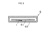
- the temperature sensor 1 is used to measure the temperature of the space between a circuit board 61 and a casing 62 of an electronic apparatus 6.
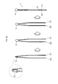
- a manufacturing method for the temperature sensor 1 mentioned above will be described with reference to Figs. 6A and 6B .
- a first disposing step as illustrated at the left end in Fig. 6A , the first and second lead wires 31 and 32 are disposed side by side.
- the first lead wire 31 is cut so as to be slighter longer than the second lead wire 32.
- the enamel coating at the distal end of each of the first and second lead wires 31 and 32 is removed.
- a bending step the distal end portions of the first and second lead wires 31 and 32 are bent.
- the distal end portion of the first lead wire 31 is bent so as to extend toward the third side face S3' at the first corner ⁇ 1 when the thermistor element 2 is inserted.
- the distal end of the second lead wire 32 is bent so as to extend toward the fourth side face S4' at the second corner ⁇ 2 when the thermistor element 2 is inserted.
- the distal end of the first lead wire 31 and the distal end of the second lead wire 32 are brought inwards and closer to each other.
- the thermistor element 2 (see Fig. 4 ) having the thermistor body 21 provided with the first and second outer electrodes 22 and 23 is prepared.
- the thermistor element 2 has the first and third side faces S1' and S3' that form the first corner ⁇ 1, and the second and fourth side face S2' and S4' that form the second corner ⁇ 2 at a position diagonal to the first corner ⁇ 1.
- the first and fourth side faces S1' and S4' further form the third corner ⁇ 3.
- the thermistor element 2 is inserted between the distal ends of both the first and second lead wires 31 and 32.
- the thermistor element 2 is disposed so that the distal end portion of the portion that is to become the first lead wire 31 extends along the first side face S1' of the thermistor element 2 and passes by the first side face S1', and that the distal end portion of the portion that is to become the second lead wire 32 extends along the second side face S2'.
- the distal end portions of the first and second lead wires 31 and 32 are bent. In this case, the bent portion at the distal end of the first lead wire 31 holds the first corner ⁇ 1 of the thermistor element 2, and the bent portion at the distal end of the second lead wire 32 holds the second corner ⁇ 2 of the thermistor element 2.
- the thermistor element 2 is fixed to the distal ends of both the first and second lead wires 31 and 32 by solder. More specifically, the first lead wire 31 is electrically connected and fixed to the first outer electrode 22 in a state in which the first and second corners ⁇ 1 and ⁇ 2 are supported by the distal ends of the first and second lead wires 31 and 32, respectively. Substantially simultaneously with this process, the second lead wire 32 is electrically connected and fixed to the second outer electrode 23. At this time, more preferably, the third corner ⁇ 3 of the thermistor element 2 is also supported by the first lead wire 31.
- the thermistor element 2 and the distal end portions of the first and second lead wires 31 and 32 are covered with an insulating resin material. Thereafter, the insulating resin material is applied with coating as required, and then cured.
- the proximal end portion of each of the first and second lead wires 31 and 32 is immersed in a high temperature solder to remove the enamel coating from this portion, and a solder coating is applied to the portion that is to become the proximal end of each of the first and second lead wires 31 and 32.
- the portions of the first and second lead wires 31 and 32 which are located on the distal end side with respect to the solder coating are fixed to each other with an adhesive or the like, and the fixing member 5 is formed.
- the distal ends of the first and second lead wires 31 and 32 are brought inwards and closer to each other.
- the thermistor element 2 is inserted between the distal ends of both the first and second lead wires 31 and 32.
- the thermistor element 2 is disposed so that the distal end portion of the first lead wire 31 extends along the first side face S1' of the thermistor element 2 and passes by the first side face S1', and that the distal end portion of the portion that is to become the second lead wire 32 extends along the second side face S2'.
- the distal ends of the first and second lead wires 31 and 32 sandwich and support the first and second corners ⁇ 1 and ⁇ 2 of the thermistor element 2 from the positive direction and negative direction of the W-axis, respectively.
- the distal end of the first lead wire 31 passes by the first side face S1', and the distal end of the second lead wire 32 extends along the second side face S2', thus increasing the contact area between the first lead wire 31 and the first side face S1' and the contact area between the second lead wire 32 and the second side face S2' in comparison to related art. Therefore, the clamping force by the first and second lead wires 31 and 32 can be increased.
- dislodging of the thermistor element 2 from the first and second lead wires 31 and 32 in the fixing step or the like can be reduced, making it possible to provide a manufacturing method for the temperature sensor 1 with improved yield rate.
- the distal end portion of the first lead wire 31 is bent toward the third side face S3', and the distal end portion of the second lead wire 32 is bent toward the fourth side face S4'. Therefore, the bent portion of the first lead wire 31 holds the first corner ⁇ 1 in such a way as to cover the first corner ⁇ 1, and the bend portion of the second lead wire 32 holds the second corner ⁇ 2 in such a way as to cover the second corner ⁇ 2.
- the first and second lead wires 31 and 32 are able to hold the thermistor element 2 in a more stable manner. Consequently, dislodging of the thermistor element 2 from the first and second lead wires 31 and 32 in the fixing step or the like can be reduced, making it possible to provide a manufacturing method for the temperature sensor 1 with improved yield rate.
- the thermistor element 2 is an NTC thermistor. However, this should not be constructed restrictively.
- the thermistor element 2 may be a PTC thermistor.
- the thermistor body 21 is typically made from a sintered ceramic obtained by mixing a predetermined amount of rare earth with barium titanate (BaTiO 3 ) and sintering the mixture.
- the thermistor element 2 is described as a multilayer chip thermistor. However, this should not be construed restrictively.
- the thermistor element 2 may be a single-chip thermistor.
- the thermistor element 2 may not necessarily be in 1005 size but may be in 3225 size, 3216 size, 2012 size, 1608 size, 0603 size, or 0402 size.
- dimensions such as the L-dimension are as summarized in Table below. Table: Size of Thermistor Element 2 Size L-dimension [mm] W-dimension [mm] T-dimension [mm] 3225 3.2 2.5 1.0 3216 3.2 1.6 1.0 2012 2.0 1.2 1.0 1608 1.6 0.8 0.4 1005 1.0 0.5 0.25 0603 0.6 0.3 0.15 0402 0.4 0.2 0.1
- first and second lead wires 31 and 32 are fixed to each other by the fixing member 5.
- the first and second lead wires 31 and 32 may be twisted so that these lead wires do not separate.
- the first and second lead wires 31 and 32 have the core wires 312 and 322 coated with the enamels 311 and 321, respectively.
- the enamels 311 and 321 may be further coated with vinyl or the like.
- the distal end portion of the first lead wire 31 is bent at the first corner ⁇ 1 toward the third side face S3', and the distal end portion of the second lead wire 32 is bent at the second corner ⁇ 2 toward the fourth side face S4'.
- the distal end portion of the first lead wire 31 may be additionally bent at the third corner ⁇ 3 toward the fourth side face S4' at an angle smaller than 90°. This makes it possible to improve the holding of the thermistor element 2 by the first and second lead wires 31 and 32.
- the distal end portion of the second lead wire 32 extends along the second side face S2' so as to pass by the portion of the second side face S2' corresponding to the second outer electrode 23 from the left end to the right end.
- the distal end portion of the second lead wire 32 may be extended to a position on the second side face S2' near the boundary between the first outer electrode 22 and the thermistor body 21, as long as the distal end portion of the second lead wire 32 does not abut on the first outer electrode 22. As a result, the holding force of the second lead wire 32 improves.
- the distal end portion of the first lead wire 31 is bent at the first corner ⁇ 1 toward the third side face S3'.
- the distal end portion of the first lead wire 31 may not be bent at the first corner ⁇ 1.
- the first and second outer electrodes 22 and 23 are opposite to each other in the L-axis direction.
- the first and second outer electrodes 22 and 23 may be opposite to each other in the W-axis direction.
- the enamels 311 and 321 may be removed from the location where the first and second lead wires 31 and 32 extend on the first and second outer electrodes 22 and 23, respectively.
- the temperature sensor and the manufacturing method for the temperature sensor according to the present invention allow an improvement in yield rate, and are suitable for use in electronic equipment or the like.
Landscapes
- Physics & Mathematics (AREA)
- Engineering & Computer Science (AREA)
- Microelectronics & Electronic Packaging (AREA)
- General Physics & Mathematics (AREA)
- Nonlinear Science (AREA)
- Electromagnetism (AREA)
- Manufacturing & Machinery (AREA)
- Thermistors And Varistors (AREA)
- Measuring Temperature Or Quantity Of Heat (AREA)
- Apparatuses And Processes For Manufacturing Resistors (AREA)
Abstract
Description
- The present invention relates to a temperature sensor including a thermistor element, and a manufacturing method for the temperature sensor.
- In related art, a temperature sensor disclosed in International Publication No.
2008/156082 exists as this type of temperature sensor. This temperature sensor is manufactured by the following procedure. - First, two lead wires of different lengths are prepared. Next, these lead wires are cut at the distal end. By this cut, the cut surfaces of the respective lead wires are inclined inward to each other, with a metal wire being exposed from the cut surface of each of the lead wires. Next, a thermistor element is disposed so that the side face of one of the lead wires is attached to the thermistor element in parallel to the longitudinal direction of the thermistor element, and that the distal end of the other lead wire supports a terminal electrode of the thermistor element.
- Next, a solder paste is applied to the junction between each of the lead wires and the corresponding terminal electrode. Thereafter, the solder paste is heated with a hot-air heater, causing the solder paste to melt. As a result, the thermistor body is fixed to both of the lead wires.
- Next, an insulating member is applied so as to cover the distal end portions of both of the lead wires and the entire thermistor element, and the insulating member is cured. Thereafter, the terminal end portion of each of the lead wires is immersed in a high temperature solder bath, thereby stripping the insulating coat covering this portion, and solder coating is applied.
- Through the above steps, the temperature sensor is completed.
- In the manufacturing method according to related art, the thermistor element is merely attached to one of the lead wires, and the terminal electrode of the thermistor element is only supported by the distal end of the other lead wire. Therefore, the thermistor element is held by the two lead wires with a relatively weak force. Consequently, at the time of solder paste application or the like, even application of a small external force causes the thermistor element to dislodge from the lead wires. As a result, the percentage of non-defective products (hereinafter, referred to as "yield rate") is low with the manufacturing method according to related art.
- Accordingly, it is an object of the present invention to provide a temperature sensor and a manufacturing method for the temperature sensor which allow an improvement in yield rate.
- According to preferred embodiments of the present invention, there is provided a manufacturing method for a temperature sensor, including a first disposing step of disposing a first lead wire and a second lead wire side by side, a preparing step of preparing a thermistor element, the thermistor element including a body, and a first outer electrode and a second outer electrode that are provided to the body, the thermistor element having a first side face and a second side face that are opposite to each other, a third side face that is adjacent to the first side face to form a first corner, and a fourth side face that is adjacent to the second side face to form a second corner at a position substantially diagonal to the first corner, a second disposing step of disposing the thermistor element so that a distal end portion of the first lead wire extends along the first side face and passes by the first side face, and a distal end portion of the second lead wire extends along the second side face, and a fixing step of electrically connecting and fixing the first lead wire to the first outer electrode, and electrically connecting and fixing the second lead wire to the second outer electrode, in a state in which the first corner and the second corner are respectively supported by the first lead wire and the second lead wire.
- According to preferred embodiments of the present invention, there is provided a temperature sensor including a thermistor element that includes a body, and a first outer electrode and a second outer electrode that are provided to the body, the thermistor element having at least a first side face and a second side face that are opposite to each other, a third side face that is adjacent to the first side face to form a first corner, and a fourth side face that is adjacent to the second side face to form a second corner at a position substantially diagonal to the first corner, a first lead wire that has a distal end portion, the distal end portion extending along the first side face and passing by the first side face, the first lead wire being electrically connected to the first outer electrode at the first corner, and a second lead wire that has a distal end portion extending along the second side face, the second lead wire being electrically connected to the second outer electrode at the second corner.
- Other features, elements, characteristics and advantages of the present invention will become more apparent from the following detailed description of preferred embodiments of the present invention with reference to the attached drawings.
-
-
Fig. 1 is a perspective view of a temperature sensor according to an embodiment of the present invention in its completed state; -
Fig. 2 illustrates in see-through view the distal end portion (a sealing member and its vicinity) of the temperature sensor illustrated inFig. 1 ; -
Fig. 3 is an enlarged view of a thermistor element illustrated inFig. 1 ; -
Fig. 4 is an enlarged view of the distal end portion of the temperature sensor illustrated inFig. 2 ; -
Fig. 5 schematically illustrates an example of application of the temperature sensor illustrated inFig. 1 ; -
Fig. 6A is a first schematic illustration of a manufacturing process for the temperature sensor illustrated inFig. 1 ; -
Fig. 6B is a second schematic illustration of the manufacturing process for the temperature sensor illustrated inFig. 1 ; -
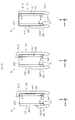
Fig. 7A is a first schematic illustration of a modification of the temperature sensor illustrated inFig. 2 ; -
Fig. 7B is a second schematic illustration of a modification of the temperature sensor illustrated inFig. 2 ; and -
Fig. 7C is a third schematic illustration of a modification of the temperature sensor illustrated inFig. 2 . - Hereinafter, a
temperature sensor 1 according to an embodiment of the present invention will be described with reference to the drawings. Prior to describing thetemperature sensor 1, an L-axis, a W-axis, and a T-axis depicted in some drawings will be defined first. The L-axis, the W-axis, and the T-axis are orthogonal to each other, and indicate the left-right direction (length direction), front-back direction (width direction), and top-bottom direction (height direction) of athermistor element 2, respectively. - As illustrated in
Figs. 1 and2 , thetemperature sensor 1 generally includes thethermistor element 2, afirst lead wire 31, asecond lead wire 32, asealing member 4, and afixing member 5. Because thethermistor element 2 and the distal ends of the first andsecond lead wires member 4, these portions are not illustrated inFig. 1 . InFig. 2 , only the contours of the sealingmember 4 are indicated by a broken line, and thethermistor element 2 and the distal ends of the first andsecond lead wires - The
thermistor element 2 is, for example, a multilayer chip thermistor. As illustrated inFig. 3 , thethermistor element 2 includes athermistor body 21, a firstouter electrode 22, and a secondouter electrode 23. - The
thermistor body 21 includes a multilayer body having a plurality of ceramic layers stacked in the T-axis direction. In some cases, a single inner electrode is provided between ceramic layers that are adjacent to each other in the T-axis direction. - The
thermistor body 21 has such a temperature characteristic that its resistance varies greatly with changing ambient temperature. In this embodiment, it is assumed that thethermistor body 21 is an NTC thermistor whose resistance decreases with increasing temperature. Such an NTC thermistor can be fabricated from a sintered oxide (sintered ceramic) obtained by mixing and sintering two to four kinds of oxides selected from the group consisting of, for example, manganese (Mn), nickel (Ni), iron (Fe), cobalt (Co), and copper (Cu). - The
thermistor body 21 has a size that is standardized by, for example, the Japanese Industrial Standards (JIS). While the size of thethermistor body 21 is not particularly limited, for example, it is assumed that thethermistor body 21 is in 1005 size. In this case, thethermistor body 21 has a dimension in the L-axis direction (that is, L-dimension) of 1.0 mm, and a dimension in the W-axis direction (that is, W-dimension) of 0.5 mm. Although the dimension in the T-axis direction (that is, T-dimension) is not specified by JIS, the toner T-dimension is, for example, 0.5 mm. It is to be noted that the L-dimension, the W-dimension, and the T-dimension are all design target values, and may not necessarily be precisely 1.0 mm, 0.5 mm, and 0.5 mm, respectively. That is, the L-dimension, the W-dimension, and the T-dimension all have tolerances. - As illustrated inside the dotted circle at the right side of
Fig. 3 , thethermistor body 21 has a substantially rectangular parallelepiped shape including a first principal face M1, a second principal face M2, a first side face S1, a second side face S2, a third side face S3, and a fourth side face S4. The first and second principal faces M1 and M2 are bottom and top faces of thethermistor body 21, respectively, and are opposite to each other at a distance of the T-dimension in the T-axis direction. The first and second side faces S1 and S2 are front and back faces of thethermistor body 21, respectively, and are opposite to each other at a distance of the W-dimension in the W-axis direction. The third and fourth side faces S3 and S4 are front side face and left side face of thethermistor body 21, respectively, and are opposite to each other at a distance of the L-dimension in the L-axis direction. - Each of the first and second
outer electrodes - The first
outer electrode 22 covers, for example, the right end portion of thethermistor body 21. More specifically, in this embodiment, the firstouter electrode 22 covers the respective right end portions of the first and second principal faces M1 and M2 and first and second side faces S1 and S2, in addition to the entirety of the third side face S3 of thethermistor body 21. - The second
outer electrode 23 covers, for example, the left end portion of thethermistor body 21. More specifically, in this embodiment, the secondouter electrode 23 covers the respective left end portions of the first and second principal faces M1 and M2 and first and second side faces S1 and S2, in addition to the entirety of the fourth side face S4 of thethermistor body 21. The secondouter electrode 23 is located at a predetermined distance in the negative direction of the L-axis with reference to the firstouter electrode 22. - Next, referring to
Fig. 4 , a first side face S1', a second side face S2', a third side face S3', and a four side face S4' of thethermistor element 2 will be described.Fig. 4 is a schematic plan view of the portion of thethermistor element 2 illustrated inFig. 2 , as seen from the negative direction of the T-axis. The first side face S1' is a face that is visible when thethermistor element 2 is seen in plan view from the negative direction of the W-axis. The first side face S1' is formed by the first side face S1 of thethermistor body 21, and the front faces of the first and secondouter electrodes thermistor element 2 is seen in plan view from the positive direction of the W-axis. The second side face S2' is formed by the second side face S2 of thethermistor body 21, and the back faces of the first and secondouter electrodes thermistor element 2 is seen in plan view from the positive direction of the L-axis. The third side face S3' is formed by the right side face of the firstouter electrode 22. The fourth side face S4' is a face that is visible when thethermistor element 2 is seen in plan view from the negative direction of the L-axis. The fourth side face S4' is formed by the left side face of the secondouter electrode 23. - The edge at the front side of the third side face S3' is substantially the same as the edge at the right side of the first side face S1'. That is, the first and third side faces S1' and S3' are adjacent to each other while sharing this edge, forming a first corner θ1 of about 90°. The edge at the back side of the fourth side face S4' is substantially the same as the edge at the left side of the second side face S2'. That is, the second and fourth side faces S2' and S4' are adjacent to each other while sharing this edge, forming a second corner θ2 of about 90°. The first and second corners θ1 and θ2 are located diagonal to each other in plan view as seen in the toner T-axis direction. Further, the first and fourth side faces S1' and S4' are also adjacent to each other at the front side, forming a third corner θ3 of about 90°.
- Now, reference will be made to
Figs. 1 and2 again. The first and secondlead wires lead wires temperature sensor 1. More specifically, as illustrated inFig. 4 , thefirst lead wire 31 is formed by acore wire 312 coated withenamel 311. Likewise, thesecond lead wire 32 is formed by acore wire 322 coated withenamel 321. Thecore wires thermistor element 2 is required to detect its own ambient temperature. Accordingly, propagation of heat from the first and secondlead wires thermistor element 2 is undesirable from the viewpoint of detecting ambient temperature. For this reason, instead of copper that has a relatively high thermal conductivity, an alloy of copper and nickel is used for thecore wires - The first and second
lead wires thermistor element 2 is secured in place while being sandwiched between the distal end portions of the first and secondlead wires thermistor element 2 is mounted. - From the viewpoint of improving the yield rate of the manufacturing process, as illustrated in
Fig. 4 , the distal end portion of thefirst lead wire 31 extends on and along the first side face S1' so as to pass by the first side face S1' from the left end to the right end. Further, the distal end portion of thefirst lead wire 31 is electrically connected and fixed to the firstouter electrode 22 by solder. For these reasons, in the distal end portion of thefirst lead wire 31, the coating of theenamel 311 is removed for at least the location to be connected to the firstouter electrode 22. Further, in the distal end portion of thefirst lead wire 31, the coating of theenamel 311 is left for the location where thefirst lead wire 31 extends on and along the portion of the first side face S1' corresponding to thethermistor body 21 and the secondouter electrode 23. This ensures electrical insulation between thefirst lead wire 31 and the secondouter electrode 23. From the viewpoint of improving the yield rate, it is further preferable that the distal end portion of thefirst lead wire 31 be bent at the corner θ1 toward the third side face S3', at an angle slightly smaller than 90°. - The distal end portion of the
second lead wire 32 extends on and along the second side face S2' so as to pass by the portion of the second side face S2' corresponding to the secondouter electrode 23 from the left end to the right end. Further, the distal end portion of thesecond lead wire 32 is electrically connected and fixed to the secondouter electrode 23 by solder. For these reasons, in the distal end portion of thesecond lead wire 32, the coating of theenamel 321 is removed for at least the location to be connected to the secondouter electrode 23. - It is further preferable that the distal end portion of the
second lead wire 32 be bent at the corner θ2 toward the fourth side face S4' at an angle slightly smaller than 90°. - For each of the first and second
lead wires enamel - The sealing
member 4 is formed of a resin material having electrical insulating property. The sealingmember 4 seals thethermistor element 2 and the distal end portions of the first and secondlead wires thermistor element 2. - The fixing
member 5 is located on the distal end side with respect to the solder-coated portion in the proximal end portion of each of the first and secondlead wires member 5 is, for example, an adhesive made of resin. The fixingmember 5 fixes the first and secondlead wires - The
temperature sensor 1 mentioned above can be adapted for a variety of applications. For example, as illustrated inFig. 5 , thetemperature sensor 1 is used to measure the temperature of the space between acircuit board 61 and acasing 62 of an electronic apparatus 6. - Next, a manufacturing method for the
temperature sensor 1 mentioned above will be described with reference toFigs. 6A and6B . First, in a first disposing step, as illustrated at the left end inFig. 6A , the first and secondlead wires Fig. 6A , thefirst lead wire 31 is cut so as to be slighter longer than thesecond lead wire 32. Next, as illustrated third from the left inFig. 6A , the enamel coating at the distal end of each of the first and secondlead wires Fig. 6A , in a bending step, the distal end portions of the first and secondlead wires first lead wire 31 is bent so as to extend toward the third side face S3' at the first corner θ1 when thethermistor element 2 is inserted. Further, the distal end of thesecond lead wire 32 is bent so as to extend toward the fourth side face S4' at the second corner θ2 when thethermistor element 2 is inserted. - Next, as illustrated fifth from the left in
Fig. 6A , in a curving step, the distal end of thefirst lead wire 31 and the distal end of thesecond lead wire 32 are brought inwards and closer to each other. - Next, as illustrated sixth from the left in
Fig. 6A , in a preparing step, the thermistor element 2 (seeFig. 4 ) having thethermistor body 21 provided with the first and secondouter electrodes thermistor element 2 has the first and third side faces S1' and S3' that form the first corner θ1, and the second and fourth side face S2' and S4' that form the second corner θ2 at a position diagonal to the first corner θ1. The first and fourth side faces S1' and S4' further form the third corner θ3. - Next, as illustrated sixth from the left in
Fig. 6A , in a second disposing step, thethermistor element 2 is inserted between the distal ends of both the first and secondlead wires Fig. 4 , thethermistor element 2 is disposed so that the distal end portion of the portion that is to become thefirst lead wire 31 extends along the first side face S1' of thethermistor element 2 and passes by the first side face S1', and that the distal end portion of the portion that is to become thesecond lead wire 32 extends along the second side face S2'. Further, in this embodiment, preferably, the distal end portions of the first and secondlead wires first lead wire 31 holds the first corner θ1 of thethermistor element 2, and the bent portion at the distal end of thesecond lead wire 32 holds the second corner θ2 of thethermistor element 2. - Next, as illustrated at the left end in
Fig. 6B , in a fixing step, thethermistor element 2 is fixed to the distal ends of both the first and secondlead wires first lead wire 31 is electrically connected and fixed to the firstouter electrode 22 in a state in which the first and second corners θ1 and θ2 are supported by the distal ends of the first and secondlead wires second lead wire 32 is electrically connected and fixed to the secondouter electrode 23. At this time, more preferably, the third corner θ3 of thethermistor element 2 is also supported by thefirst lead wire 31. - Next, as illustrated second from the left in
Fig. 6B , to form the sealingmember 4, thethermistor element 2 and the distal end portions of the first and secondlead wires - Next, as illustrated third from the left in
Fig. 6B , the proximal end portion of each of the first and secondlead wires lead wires Fig. 6B , the portions of the first and secondlead wires member 5 is formed. - As mentioned above, in the manufacturing process for the
temperature sensor 1 according to this embodiment, in the curving step, the distal ends of the first and secondlead wires thermistor element 2 is inserted between the distal ends of both the first and secondlead wires Fig. 4 , thethermistor element 2 is disposed so that the distal end portion of thefirst lead wire 31 extends along the first side face S1' of thethermistor element 2 and passes by the first side face S1', and that the distal end portion of the portion that is to become thesecond lead wire 32 extends along the second side face S2'. - Therefore, after the second disposing step, the distal ends of the first and second
lead wires thermistor element 2 from the positive direction and negative direction of the W-axis, respectively. At this time, the distal end of thefirst lead wire 31 passes by the first side face S1', and the distal end of thesecond lead wire 32 extends along the second side face S2', thus increasing the contact area between thefirst lead wire 31 and the first side face S1' and the contact area between thesecond lead wire 32 and the second side face S2' in comparison to related art. Therefore, the clamping force by the first and secondlead wires thermistor element 2 from the first and secondlead wires temperature sensor 1 with improved yield rate. - In this embodiment, preferably, the distal end portion of the
first lead wire 31 is bent toward the third side face S3', and the distal end portion of thesecond lead wire 32 is bent toward the fourth side face S4'. Therefore, the bent portion of thefirst lead wire 31 holds the first corner θ1 in such a way as to cover the first corner θ1, and the bend portion of thesecond lead wire 32 holds the second corner θ2 in such a way as to cover the second corner θ2. As a result, the first and secondlead wires thermistor element 2 in a more stable manner. Consequently, dislodging of thethermistor element 2 from the first and secondlead wires temperature sensor 1 with improved yield rate. - In the above embodiment, the
thermistor element 2 is an NTC thermistor. However, this should not be constructed restrictively. Thethermistor element 2 may be a PTC thermistor. In this case, thethermistor body 21 is typically made from a sintered ceramic obtained by mixing a predetermined amount of rare earth with barium titanate (BaTiO3) and sintering the mixture. - In the above embodiment, the
thermistor element 2 is described as a multilayer chip thermistor. However, this should not be construed restrictively. Thethermistor element 2 may be a single-chip thermistor. - The
thermistor element 2 may not necessarily be in 1005 size but may be in 3225 size, 3216 size, 2012 size, 1608 size, 0603 size, or 0402 size. For these sizes, dimensions such as the L-dimension are as summarized in Table below.Table: Size of Thermistor Element 2Size L-dimension [mm] W-dimension [mm] T-dimension [mm] 3225 3.2 2.5 1.0 3216 3.2 1.6 1.0 2012 2.0 1.2 1.0 1608 1.6 0.8 0.4 1005 1.0 0.5 0.25 0603 0.6 0.3 0.15 0402 0.4 0.2 0.1 - In the above embodiment, the first and second
lead wires member 5. However, this should not be construed restrictively. The first and secondlead wires - In the above embodiment, the first and second
lead wires core wires enamels lead wires enamels - Next, several modifications of the
temperature sensor 1 will be described with reference toFigs. 7A to 7C . In the example illustrated inFig. 4 , the distal end portion of thefirst lead wire 31 is bent at the first corner θ1 toward the third side face S3', and the distal end portion of thesecond lead wire 32 is bent at the second corner θ2 toward the fourth side face S4'. However, this should not be construed restrictively. As illustrated at the left end inFig. 7A , in thetemperature sensor 1, the distal end portion of thefirst lead wire 31 may be additionally bent at the third corner θ3 toward the fourth side face S4' at an angle smaller than 90°. This makes it possible to improve the holding of thethermistor element 2 by the first and secondlead wires - In the example illustrated in
Fig. 4 , the distal end portion of thesecond lead wire 32 extends along the second side face S2' so as to pass by the portion of the second side face S2' corresponding to the secondouter electrode 23 from the left end to the right end. However, this should not be construed restrictively. As illustrated in the middle inFig. 7A , the distal end portion of thesecond lead wire 32 may be extended to a position on the second side face S2' near the boundary between the firstouter electrode 22 and thethermistor body 21, as long as the distal end portion of thesecond lead wire 32 does not abut on the firstouter electrode 22. As a result, the holding force of thesecond lead wire 32 improves. - In the example illustrated in
Fig. 4 , the distal end portion of thefirst lead wire 31 is bent at the first corner θ1 toward the third side face S3'. However, as illustrated at the right end inFig. 7A , the distal end portion of thefirst lead wire 31 may not be bent at the first corner θ1. - In the foregoing example, in the
thermistor element 2, the first and secondouter electrodes Fig. 7B , the first and secondouter electrodes Fig. 7C , in the distal end portions of the first and secondlead wires enamels lead wires outer electrodes - The temperature sensor and the manufacturing method for the temperature sensor according to the present invention allow an improvement in yield rate, and are suitable for use in electronic equipment or the like.
- While preferred embodiments of the invention have been described above, it is to be understood that variations and modifications will be apparent to those skilled in the art without departing from the scope and spirit of the invention. The scope of the invention, therefore, is to be determined solely by the following claims.
Claims (8)
- A manufacturing method for a temperature sensor, comprising:a first disposing step of disposing a first lead wire and a second lead wire side by side;a preparing step of preparing a thermistor element, the thermistor element including a body, and a first outer electrode and a second outer electrode that are provided to the body, the thermistor element havinga first side face and a second side face that are opposite to each other,a third side face that is adjacent to the first side face to form a first corner, anda fourth side face that is adjacent to the second side face to form a second corner at a position substantially diagonal to the first corner;a second disposing step of disposing the thermistor element so that a distal end portion of the first lead wire extends along the first side face and passes by the first side face, and a distal end portion of the second lead wire extends along the second side face; anda fixing step of electrically connecting and fixing the first lead wire to the first outer electrode, and electrically connecting and fixing the second lead wire to the second outer electrode, in a state in which the first corner and the second corner are respectively supported by the first lead wire and the second lead wire.
- The manufacturing method for a temperature sensor according to Claim 1, wherein:the first side face is further adjacent to the fourth side face to form a third corner; andin the fixing step, both the first corner and the third corner are supported by the first lead wire, and the second corner is supported by the second lead wire.
- The manufacturing method for a temperature sensor according to Claim 1 or 2, further comprising, prior to the second disposing step, a bending step of bending the distal end portion of the first lead wire at the first corner toward the third side face.
- The manufacturing method for a temperature sensor according to Claim 3, wherein the bending step further includes bending the distal end portion of the second lead wire at the second corner toward the fourth side face.
- A temperature sensor comprising:a thermistor element that includes a body, and a first outer electrode and a second outer electrode that are provided to the body, the thermistor element having at leasta first side face and a second side face that are opposite to each other,a third side face that is adjacent to the first side face to form a first corner, anda fourth side face that is adjacent to the second side face to form a second corner at a position substantially diagonal to the first corner;a first lead wire that has a distal end portion, the distal end portion extending along the first side face and passing by the first side face, the first lead wire being electrically connected to the first outer electrode at the first corner; anda second lead wire that has a distal end portion extending along the second side face, the second lead wire being electrically connected to the second outer electrode at the second corner.
- The temperature sensor according to Claim 5, wherein the distal end portion of the first lead wire is bent at the first corner toward the third side face.
- The temperature sensor according to Claim 5 or 6, wherein the distal end portion of the second lead wire is bent at the second corner toward the fourth side face.
- The temperature sensor according to any one of Claims 5 to 7, wherein each of the first lead wire and the second lead wire is a single wire.
Applications Claiming Priority (1)
| Application Number | Priority Date | Filing Date | Title |
|---|---|---|---|
| JP2014005565A JP5880583B2 (en) | 2014-01-16 | 2014-01-16 | Temperature sensor and manufacturing method |
Publications (2)
| Publication Number | Publication Date |
|---|---|
| EP2896944A1 true EP2896944A1 (en) | 2015-07-22 |
| EP2896944B1 EP2896944B1 (en) | 2018-01-31 |
Family
ID=51987086
Family Applications (1)
| Application Number | Title | Priority Date | Filing Date |
|---|---|---|---|
| EP14195651.6A Active EP2896944B1 (en) | 2014-01-16 | 2014-12-01 | Temperature sensor and manufacturing method for temperature sensor |
Country Status (6)
| Country | Link |
|---|---|
| US (1) | US9812236B2 (en) |
| EP (1) | EP2896944B1 (en) |
| JP (1) | JP5880583B2 (en) |
| KR (1) | KR101645020B1 (en) |
| CN (1) | CN104792432B (en) |
| TW (1) | TWI540314B (en) |
Families Citing this family (2)
| Publication number | Priority date | Publication date | Assignee | Title |
|---|---|---|---|---|
| DE102016101248A1 (en) * | 2015-11-02 | 2017-05-04 | Epcos Ag | Sensor element and method for producing a sensor element |
| CN112362178B (en) * | 2019-06-26 | 2023-05-09 | 兴勤(宜昌)电子有限公司 | Double-sided automatic welding equipment for glass packaging temperature sensor |
Citations (4)
| Publication number | Priority date | Publication date | Assignee | Title |
|---|---|---|---|---|
| US4712085A (en) * | 1984-10-30 | 1987-12-08 | Tdk Corporation | Thermistor element and method of manufacturing the same |
| JPH02270303A (en) * | 1989-04-11 | 1990-11-05 | Matsushita Electric Ind Co Ltd | Manufacturing method of glass-sealed thermistor |
| WO2008156082A1 (en) | 2007-06-19 | 2008-12-24 | Murata Manufacturing Co., Ltd. | Temperature sensor with lead wires |
| US20100214054A1 (en) * | 2009-02-20 | 2010-08-26 | Hirokazu Kobayashi | Thermistor device |
Family Cites Families (10)
| Publication number | Priority date | Publication date | Assignee | Title |
|---|---|---|---|---|
| GB2207297B (en) * | 1987-07-11 | 1991-07-31 | Stc Plc | Encapsulated electronic components |
| JPH09297069A (en) * | 1996-05-07 | 1997-11-18 | Tdk Corp | Temperature detecting sensor |
| JP3648465B2 (en) * | 2001-06-22 | 2005-05-18 | Tdk株式会社 | NTC thermistor for temperature detection and manufacturing method thereof |
| JP3476800B2 (en) * | 2001-08-22 | 2003-12-10 | Tdk株式会社 | Radial lead type multilayer ceramic electronic components |
| JP2004212269A (en) * | 2003-01-07 | 2004-07-29 | Ngk Spark Plug Co Ltd | Temperature sensor |
| JP2004273494A (en) * | 2003-03-05 | 2004-09-30 | Rinnai Corp | Thermistor and its manufacturing method |
| JP2010073731A (en) * | 2008-09-16 | 2010-04-02 | Murata Mfg Co Ltd | Electronic component with lead wire |
| JP5326826B2 (en) * | 2009-06-02 | 2013-10-30 | 三菱マテリアル株式会社 | Temperature sensor |
| JP5141791B2 (en) * | 2010-08-30 | 2013-02-13 | 株式会社デンソー | Temperature sensor |
| JP5847517B2 (en) * | 2011-09-28 | 2016-01-20 | 株式会社芝浦電子 | Hydrogen filling system |
-
2014
- 2014-01-16 JP JP2014005565A patent/JP5880583B2/en active Active
- 2014-12-01 EP EP14195651.6A patent/EP2896944B1/en active Active
- 2014-12-04 KR KR1020140173217A patent/KR101645020B1/en active Active
- 2014-12-08 US US14/562,981 patent/US9812236B2/en active Active
- 2014-12-25 TW TW103145562A patent/TWI540314B/en active
- 2014-12-25 CN CN201410842142.2A patent/CN104792432B/en active Active
Patent Citations (4)
| Publication number | Priority date | Publication date | Assignee | Title |
|---|---|---|---|---|
| US4712085A (en) * | 1984-10-30 | 1987-12-08 | Tdk Corporation | Thermistor element and method of manufacturing the same |
| JPH02270303A (en) * | 1989-04-11 | 1990-11-05 | Matsushita Electric Ind Co Ltd | Manufacturing method of glass-sealed thermistor |
| WO2008156082A1 (en) | 2007-06-19 | 2008-12-24 | Murata Manufacturing Co., Ltd. | Temperature sensor with lead wires |
| US20100214054A1 (en) * | 2009-02-20 | 2010-08-26 | Hirokazu Kobayashi | Thermistor device |
Also Published As
| Publication number | Publication date |
|---|---|
| KR20150085774A (en) | 2015-07-24 |
| JP5880583B2 (en) | 2016-03-09 |
| JP2015133461A (en) | 2015-07-23 |
| TWI540314B (en) | 2016-07-01 |
| CN104792432A (en) | 2015-07-22 |
| KR101645020B1 (en) | 2016-08-02 |
| US20150200043A1 (en) | 2015-07-16 |
| EP2896944B1 (en) | 2018-01-31 |
| US9812236B2 (en) | 2017-11-07 |
| CN104792432B (en) | 2017-11-14 |
| TW201530107A (en) | 2015-08-01 |
Similar Documents
| Publication | Publication Date | Title |
|---|---|---|
| CN103098150B (en) | Surface Mount Varistors | |
| US10224138B2 (en) | Electrode structure and the corresponding electrical component using the same and the fabrication method thereof | |
| JP6286914B2 (en) | Ceramic electronic components | |
| JP6937176B2 (en) | Electronic components, electronic devices, and methods for manufacturing electronic components | |
| TWI743125B (en) | High performance and reliability solid electrolytic tantalum capacitors and screening method | |
| CN101677151A (en) | Electronic component with lead wire | |
| JP6540069B2 (en) | Multilayer feedthrough capacitor | |
| KR20190033765A (en) | Electronic component | |
| US9620266B2 (en) | Electrical device | |
| JP6278994B2 (en) | Power filter | |
| EP2896944B1 (en) | Temperature sensor and manufacturing method for temperature sensor | |
| KR20150105691A (en) | Chip type coil component and board for mounting the same | |
| US11056263B2 (en) | Inductor | |
| US11551872B2 (en) | Multilayer ceramic capacitor | |
| JP5262448B2 (en) | Thermistor | |
| US9159490B2 (en) | Solid electrolytic capacitor package structure and method of manufacturing the same, and conductive unit | |
| JP2024507178A (en) | Surface mount metal oxide varistor device | |
| JP2007073883A (en) | Chip capacitor | |
| WO2014203846A1 (en) | Solid electrolytic capacitor, anode lead connection method for same, and production method for solid electrolytic capacitor | |
| KR20130076599A (en) | Resistor and method for manufacturing the same | |
| JP6996486B2 (en) | Winding inductor component | |
| CN214478032U (en) | RIP sleeve pipe that possesses buffer layer structure | |
| JP5941080B2 (en) | Tantalum capacitor and manufacturing method thereof | |
| JP2007180523A (en) | Thermistor | |
| JP6723690B2 (en) | Coated lead type electronic component and manufacturing method thereof |
Legal Events
| Date | Code | Title | Description |
|---|---|---|---|
| PUAI | Public reference made under article 153(3) epc to a published international application that has entered the european phase |
Free format text: ORIGINAL CODE: 0009012 |
|
| 17P | Request for examination filed |
Effective date: 20141201 |
|
| AK | Designated contracting states |
Kind code of ref document: A1 Designated state(s): AL AT BE BG CH CY CZ DE DK EE ES FI FR GB GR HR HU IE IS IT LI LT LU LV MC MK MT NL NO PL PT RO RS SE SI SK SM TR |
|
| AX | Request for extension of the european patent |
Extension state: BA ME |
|
| 17P | Request for examination filed |
Effective date: 20160112 |
|
| RBV | Designated contracting states (corrected) |
Designated state(s): AL AT BE BG CH CY CZ DE DK EE ES FI FR GB GR HR HU IE IS IT LI LT LU LV MC MK MT NL NO PL PT RO RS SE SI SK SM TR |
|
| GRAP | Despatch of communication of intention to grant a patent |
Free format text: ORIGINAL CODE: EPIDOSNIGR1 |
|
| INTG | Intention to grant announced |
Effective date: 20170803 |
|
| GRAS | Grant fee paid |
Free format text: ORIGINAL CODE: EPIDOSNIGR3 |
|
| GRAA | (expected) grant |
Free format text: ORIGINAL CODE: 0009210 |
|
| AK | Designated contracting states |
Kind code of ref document: B1 Designated state(s): AL AT BE BG CH CY CZ DE DK EE ES FI FR GB GR HR HU IE IS IT LI LT LU LV MC MK MT NL NO PL PT RO RS SE SI SK SM TR |
|
| REG | Reference to a national code |
Ref country code: GB Ref legal event code: FG4D Ref country code: CH Ref legal event code: EP |
|
| REG | Reference to a national code |
Ref country code: AT Ref legal event code: REF Ref document number: 967815 Country of ref document: AT Kind code of ref document: T Effective date: 20180215 |
|
| REG | Reference to a national code |
Ref country code: IE Ref legal event code: FG4D |
|
| REG | Reference to a national code |
Ref country code: DE Ref legal event code: R096 Ref document number: 602014020318 Country of ref document: DE |
|
| REG | Reference to a national code |
Ref country code: NL Ref legal event code: MP Effective date: 20180131 |
|
| REG | Reference to a national code |
Ref country code: LT Ref legal event code: MG4D |
|
| REG | Reference to a national code |
Ref country code: AT Ref legal event code: MK05 Ref document number: 967815 Country of ref document: AT Kind code of ref document: T Effective date: 20180131 |
|
| PG25 | Lapsed in a contracting state [announced via postgrant information from national office to epo] |
Ref country code: NO Free format text: LAPSE BECAUSE OF FAILURE TO SUBMIT A TRANSLATION OF THE DESCRIPTION OR TO PAY THE FEE WITHIN THE PRESCRIBED TIME-LIMIT Effective date: 20180430 Ref country code: ES Free format text: LAPSE BECAUSE OF FAILURE TO SUBMIT A TRANSLATION OF THE DESCRIPTION OR TO PAY THE FEE WITHIN THE PRESCRIBED TIME-LIMIT Effective date: 20180131 Ref country code: LT Free format text: LAPSE BECAUSE OF FAILURE TO SUBMIT A TRANSLATION OF THE DESCRIPTION OR TO PAY THE FEE WITHIN THE PRESCRIBED TIME-LIMIT Effective date: 20180131 Ref country code: NL Free format text: LAPSE BECAUSE OF FAILURE TO SUBMIT A TRANSLATION OF THE DESCRIPTION OR TO PAY THE FEE WITHIN THE PRESCRIBED TIME-LIMIT Effective date: 20180131 Ref country code: HR Free format text: LAPSE BECAUSE OF FAILURE TO SUBMIT A TRANSLATION OF THE DESCRIPTION OR TO PAY THE FEE WITHIN THE PRESCRIBED TIME-LIMIT Effective date: 20180131 Ref country code: FI Free format text: LAPSE BECAUSE OF FAILURE TO SUBMIT A TRANSLATION OF THE DESCRIPTION OR TO PAY THE FEE WITHIN THE PRESCRIBED TIME-LIMIT Effective date: 20180131 |
|
| PG25 | Lapsed in a contracting state [announced via postgrant information from national office to epo] |
Ref country code: IS Free format text: LAPSE BECAUSE OF FAILURE TO SUBMIT A TRANSLATION OF THE DESCRIPTION OR TO PAY THE FEE WITHIN THE PRESCRIBED TIME-LIMIT Effective date: 20180531 Ref country code: GR Free format text: LAPSE BECAUSE OF FAILURE TO SUBMIT A TRANSLATION OF THE DESCRIPTION OR TO PAY THE FEE WITHIN THE PRESCRIBED TIME-LIMIT Effective date: 20180501 Ref country code: PL Free format text: LAPSE BECAUSE OF FAILURE TO SUBMIT A TRANSLATION OF THE DESCRIPTION OR TO PAY THE FEE WITHIN THE PRESCRIBED TIME-LIMIT Effective date: 20180131 Ref country code: SE Free format text: LAPSE BECAUSE OF FAILURE TO SUBMIT A TRANSLATION OF THE DESCRIPTION OR TO PAY THE FEE WITHIN THE PRESCRIBED TIME-LIMIT Effective date: 20180131 Ref country code: LV Free format text: LAPSE BECAUSE OF FAILURE TO SUBMIT A TRANSLATION OF THE DESCRIPTION OR TO PAY THE FEE WITHIN THE PRESCRIBED TIME-LIMIT Effective date: 20180131 Ref country code: AT Free format text: LAPSE BECAUSE OF FAILURE TO SUBMIT A TRANSLATION OF THE DESCRIPTION OR TO PAY THE FEE WITHIN THE PRESCRIBED TIME-LIMIT Effective date: 20180131 Ref country code: BG Free format text: LAPSE BECAUSE OF FAILURE TO SUBMIT A TRANSLATION OF THE DESCRIPTION OR TO PAY THE FEE WITHIN THE PRESCRIBED TIME-LIMIT Effective date: 20180430 Ref country code: RS Free format text: LAPSE BECAUSE OF FAILURE TO SUBMIT A TRANSLATION OF THE DESCRIPTION OR TO PAY THE FEE WITHIN THE PRESCRIBED TIME-LIMIT Effective date: 20180131 |
|
| PG25 | Lapsed in a contracting state [announced via postgrant information from national office to epo] |
Ref country code: EE Free format text: LAPSE BECAUSE OF FAILURE TO SUBMIT A TRANSLATION OF THE DESCRIPTION OR TO PAY THE FEE WITHIN THE PRESCRIBED TIME-LIMIT Effective date: 20180131 Ref country code: AL Free format text: LAPSE BECAUSE OF FAILURE TO SUBMIT A TRANSLATION OF THE DESCRIPTION OR TO PAY THE FEE WITHIN THE PRESCRIBED TIME-LIMIT Effective date: 20180131 Ref country code: RO Free format text: LAPSE BECAUSE OF FAILURE TO SUBMIT A TRANSLATION OF THE DESCRIPTION OR TO PAY THE FEE WITHIN THE PRESCRIBED TIME-LIMIT Effective date: 20180131 Ref country code: IT Free format text: LAPSE BECAUSE OF FAILURE TO SUBMIT A TRANSLATION OF THE DESCRIPTION OR TO PAY THE FEE WITHIN THE PRESCRIBED TIME-LIMIT Effective date: 20180131 |
|
| REG | Reference to a national code |
Ref country code: DE Ref legal event code: R097 Ref document number: 602014020318 Country of ref document: DE |
|
| PG25 | Lapsed in a contracting state [announced via postgrant information from national office to epo] |
Ref country code: DK Free format text: LAPSE BECAUSE OF FAILURE TO SUBMIT A TRANSLATION OF THE DESCRIPTION OR TO PAY THE FEE WITHIN THE PRESCRIBED TIME-LIMIT Effective date: 20180131 Ref country code: CZ Free format text: LAPSE BECAUSE OF FAILURE TO SUBMIT A TRANSLATION OF THE DESCRIPTION OR TO PAY THE FEE WITHIN THE PRESCRIBED TIME-LIMIT Effective date: 20180131 Ref country code: SM Free format text: LAPSE BECAUSE OF FAILURE TO SUBMIT A TRANSLATION OF THE DESCRIPTION OR TO PAY THE FEE WITHIN THE PRESCRIBED TIME-LIMIT Effective date: 20180131 Ref country code: SK Free format text: LAPSE BECAUSE OF FAILURE TO SUBMIT A TRANSLATION OF THE DESCRIPTION OR TO PAY THE FEE WITHIN THE PRESCRIBED TIME-LIMIT Effective date: 20180131 |
|
| PLBE | No opposition filed within time limit |
Free format text: ORIGINAL CODE: 0009261 |
|
| STAA | Information on the status of an ep patent application or granted ep patent |
Free format text: STATUS: NO OPPOSITION FILED WITHIN TIME LIMIT |
|
| 26N | No opposition filed |
Effective date: 20181102 |
|
| PG25 | Lapsed in a contracting state [announced via postgrant information from national office to epo] |
Ref country code: SI Free format text: LAPSE BECAUSE OF FAILURE TO SUBMIT A TRANSLATION OF THE DESCRIPTION OR TO PAY THE FEE WITHIN THE PRESCRIBED TIME-LIMIT Effective date: 20180131 |
|
| REG | Reference to a national code |
Ref country code: CH Ref legal event code: PL |
|
| GBPC | Gb: european patent ceased through non-payment of renewal fee |
Effective date: 20181201 |
|
| PG25 | Lapsed in a contracting state [announced via postgrant information from national office to epo] |
Ref country code: MC Free format text: LAPSE BECAUSE OF FAILURE TO SUBMIT A TRANSLATION OF THE DESCRIPTION OR TO PAY THE FEE WITHIN THE PRESCRIBED TIME-LIMIT Effective date: 20180131 Ref country code: LU Free format text: LAPSE BECAUSE OF NON-PAYMENT OF DUE FEES Effective date: 20181201 |
|
| REG | Reference to a national code |
Ref country code: IE Ref legal event code: MM4A |
|
| REG | Reference to a national code |
Ref country code: BE Ref legal event code: MM Effective date: 20181231 |
|
| PG25 | Lapsed in a contracting state [announced via postgrant information from national office to epo] |
Ref country code: IE Free format text: LAPSE BECAUSE OF NON-PAYMENT OF DUE FEES Effective date: 20181201 Ref country code: FR Free format text: LAPSE BECAUSE OF NON-PAYMENT OF DUE FEES Effective date: 20181231 |
|
| PG25 | Lapsed in a contracting state [announced via postgrant information from national office to epo] |
Ref country code: BE Free format text: LAPSE BECAUSE OF NON-PAYMENT OF DUE FEES Effective date: 20181231 |
|
| PG25 | Lapsed in a contracting state [announced via postgrant information from national office to epo] |
Ref country code: GB Free format text: LAPSE BECAUSE OF NON-PAYMENT OF DUE FEES Effective date: 20181201 Ref country code: LI Free format text: LAPSE BECAUSE OF NON-PAYMENT OF DUE FEES Effective date: 20181231 Ref country code: CH Free format text: LAPSE BECAUSE OF NON-PAYMENT OF DUE FEES Effective date: 20181231 |
|
| PG25 | Lapsed in a contracting state [announced via postgrant information from national office to epo] |
Ref country code: MT Free format text: LAPSE BECAUSE OF NON-PAYMENT OF DUE FEES Effective date: 20181201 |
|
| PG25 | Lapsed in a contracting state [announced via postgrant information from national office to epo] |
Ref country code: TR Free format text: LAPSE BECAUSE OF FAILURE TO SUBMIT A TRANSLATION OF THE DESCRIPTION OR TO PAY THE FEE WITHIN THE PRESCRIBED TIME-LIMIT Effective date: 20180131 |
|
| PG25 | Lapsed in a contracting state [announced via postgrant information from national office to epo] |
Ref country code: PT Free format text: LAPSE BECAUSE OF FAILURE TO SUBMIT A TRANSLATION OF THE DESCRIPTION OR TO PAY THE FEE WITHIN THE PRESCRIBED TIME-LIMIT Effective date: 20180131 |
|
| PG25 | Lapsed in a contracting state [announced via postgrant information from national office to epo] |
Ref country code: CY Free format text: LAPSE BECAUSE OF FAILURE TO SUBMIT A TRANSLATION OF THE DESCRIPTION OR TO PAY THE FEE WITHIN THE PRESCRIBED TIME-LIMIT Effective date: 20180131 Ref country code: MK Free format text: LAPSE BECAUSE OF NON-PAYMENT OF DUE FEES Effective date: 20180131 Ref country code: HU Free format text: LAPSE BECAUSE OF FAILURE TO SUBMIT A TRANSLATION OF THE DESCRIPTION OR TO PAY THE FEE WITHIN THE PRESCRIBED TIME-LIMIT; INVALID AB INITIO Effective date: 20141201 |
|
| PGFP | Annual fee paid to national office [announced via postgrant information from national office to epo] |
Ref country code: DE Payment date: 20251211 Year of fee payment: 12 |