EP2895899B1 - Procédé de formation de matières à cristaux photoniques - Google Patents
Procédé de formation de matières à cristaux photoniques Download PDFInfo
- Publication number
- EP2895899B1 EP2895899B1 EP13763287.3A EP13763287A EP2895899B1 EP 2895899 B1 EP2895899 B1 EP 2895899B1 EP 13763287 A EP13763287 A EP 13763287A EP 2895899 B1 EP2895899 B1 EP 2895899B1
- Authority
- EP
- European Patent Office
- Prior art keywords
- substrate
- array
- particles
- contact surface
- matrix
- Prior art date
- Legal status (The legal status is an assumption and is not a legal conclusion. Google has not performed a legal analysis and makes no representation as to the accuracy of the status listed.)
- Not-in-force
Links
- 238000000034 method Methods 0.000 title claims description 75
- 239000000463 material Substances 0.000 title claims description 73
- 239000004038 photonic crystal Substances 0.000 title claims description 27
- 239000000758 substrate Substances 0.000 claims description 126
- 239000011347 resin Substances 0.000 claims description 49
- 229920005989 resin Polymers 0.000 claims description 49
- 238000005530 etching Methods 0.000 claims description 43
- 239000011230 binding agent Substances 0.000 claims description 38
- 239000011159 matrix material Substances 0.000 claims description 37
- 239000002245 particle Substances 0.000 claims description 31
- 239000003795 chemical substances by application Substances 0.000 claims description 27
- 238000001035 drying Methods 0.000 claims description 24
- VYPSYNLAJGMNEJ-UHFFFAOYSA-N Silicium dioxide Chemical compound O=[Si]=O VYPSYNLAJGMNEJ-UHFFFAOYSA-N 0.000 claims description 23
- 230000008569 process Effects 0.000 claims description 20
- KRHYYFGTRYWZRS-UHFFFAOYSA-N Fluorane Chemical compound F KRHYYFGTRYWZRS-UHFFFAOYSA-N 0.000 claims description 15
- 230000000694 effects Effects 0.000 claims description 8
- -1 polyethylene Polymers 0.000 claims description 8
- 239000006227 byproduct Substances 0.000 claims description 5
- 238000004804 winding Methods 0.000 claims description 5
- 239000010409 thin film Substances 0.000 claims description 4
- 239000004698 Polyethylene Substances 0.000 claims description 3
- 229920000573 polyethylene Polymers 0.000 claims description 3
- 238000007598 dipping method Methods 0.000 claims description 2
- 238000005507 spraying Methods 0.000 claims description 2
- 238000000576 coating method Methods 0.000 description 54
- 239000011248 coating agent Substances 0.000 description 46
- 239000002904 solvent Substances 0.000 description 20
- 239000011022 opal Substances 0.000 description 19
- 238000001723 curing Methods 0.000 description 16
- 239000006185 dispersion Substances 0.000 description 15
- 230000003287 optical effect Effects 0.000 description 12
- 238000001338 self-assembly Methods 0.000 description 11
- 239000004005 microsphere Substances 0.000 description 10
- 229920000642 polymer Polymers 0.000 description 10
- 239000000654 additive Substances 0.000 description 9
- 238000004519 manufacturing process Methods 0.000 description 9
- 239000000377 silicon dioxide Substances 0.000 description 8
- LYCAIKOWRPUZTN-UHFFFAOYSA-N Ethylene glycol Chemical compound OCCO LYCAIKOWRPUZTN-UHFFFAOYSA-N 0.000 description 7
- 238000012545 processing Methods 0.000 description 7
- OKKJLVBELUTLKV-UHFFFAOYSA-N Methanol Chemical compound OC OKKJLVBELUTLKV-UHFFFAOYSA-N 0.000 description 6
- 230000032798 delamination Effects 0.000 description 6
- 239000010408 film Substances 0.000 description 6
- 238000003475 lamination Methods 0.000 description 6
- XLYOFNOQVPJJNP-UHFFFAOYSA-N water Substances O XLYOFNOQVPJJNP-UHFFFAOYSA-N 0.000 description 6
- 239000000805 composite resin Substances 0.000 description 5
- 230000003993 interaction Effects 0.000 description 5
- 239000007788 liquid Substances 0.000 description 5
- 239000000203 mixture Substances 0.000 description 5
- QPJSUIGXIBEQAC-UHFFFAOYSA-N n-(2,4-dichloro-5-propan-2-yloxyphenyl)acetamide Chemical compound CC(C)OC1=CC(NC(C)=O)=C(Cl)C=C1Cl QPJSUIGXIBEQAC-UHFFFAOYSA-N 0.000 description 5
- 229920000139 polyethylene terephthalate Polymers 0.000 description 5
- IJGRMHOSHXDMSA-UHFFFAOYSA-N Atomic nitrogen Chemical compound N#N IJGRMHOSHXDMSA-UHFFFAOYSA-N 0.000 description 4
- GWEVSGVZZGPLCZ-UHFFFAOYSA-N Titan oxide Chemical compound O=[Ti]=O GWEVSGVZZGPLCZ-UHFFFAOYSA-N 0.000 description 4
- 238000013459 approach Methods 0.000 description 4
- 239000002131 composite material Substances 0.000 description 4
- 238000009792 diffusion process Methods 0.000 description 4
- 239000012530 fluid Substances 0.000 description 4
- 239000000047 product Substances 0.000 description 4
- 230000002441 reversible effect Effects 0.000 description 4
- 239000000243 solution Substances 0.000 description 4
- IAZDPXIOMUYVGZ-UHFFFAOYSA-N Dimethylsulphoxide Chemical compound CS(C)=O IAZDPXIOMUYVGZ-UHFFFAOYSA-N 0.000 description 3
- DNIAPMSPPWPWGF-UHFFFAOYSA-N Propylene glycol Chemical compound CC(O)CO DNIAPMSPPWPWGF-UHFFFAOYSA-N 0.000 description 3
- 238000003848 UV Light-Curing Methods 0.000 description 3
- 230000008901 benefit Effects 0.000 description 3
- 238000009835 boiling Methods 0.000 description 3
- 238000010894 electron beam technology Methods 0.000 description 3
- 238000007756 gravure coating Methods 0.000 description 3
- 230000002209 hydrophobic effect Effects 0.000 description 3
- 239000003999 initiator Substances 0.000 description 3
- 229910044991 metal oxide Inorganic materials 0.000 description 3
- 150000004706 metal oxides Chemical class 0.000 description 3
- 229920001343 polytetrafluoroethylene Polymers 0.000 description 3
- 239000007787 solid Substances 0.000 description 3
- 238000012546 transfer Methods 0.000 description 3
- 238000005406 washing Methods 0.000 description 3
- KBPLFHHGFOOTCA-UHFFFAOYSA-N 1-Octanol Chemical compound CCCCCCCCO KBPLFHHGFOOTCA-UHFFFAOYSA-N 0.000 description 2
- 229920002799 BoPET Polymers 0.000 description 2
- LFQSCWFLJHTTHZ-UHFFFAOYSA-N Ethanol Chemical compound CCO LFQSCWFLJHTTHZ-UHFFFAOYSA-N 0.000 description 2
- XEEYBQQBJWHFJM-UHFFFAOYSA-N Iron Chemical compound [Fe] XEEYBQQBJWHFJM-UHFFFAOYSA-N 0.000 description 2
- LRHPLDYGYMQRHN-UHFFFAOYSA-N N-Butanol Chemical compound CCCCO LRHPLDYGYMQRHN-UHFFFAOYSA-N 0.000 description 2
- 239000004793 Polystyrene Substances 0.000 description 2
- MCMNRKCIXSYSNV-UHFFFAOYSA-N Zirconium dioxide Chemical compound O=[Zr]=O MCMNRKCIXSYSNV-UHFFFAOYSA-N 0.000 description 2
- 238000005299 abrasion Methods 0.000 description 2
- 239000002253 acid Substances 0.000 description 2
- 150000007513 acids Chemical class 0.000 description 2
- 150000001298 alcohols Chemical class 0.000 description 2
- 239000007864 aqueous solution Substances 0.000 description 2
- 238000003491 array Methods 0.000 description 2
- 230000008859 change Effects 0.000 description 2
- 239000008199 coating composition Substances 0.000 description 2
- 239000000470 constituent Substances 0.000 description 2
- 239000013078 crystal Substances 0.000 description 2
- 230000007547 defect Effects 0.000 description 2
- 230000005670 electromagnetic radiation Effects 0.000 description 2
- 238000001125 extrusion Methods 0.000 description 2
- 239000007789 gas Substances 0.000 description 2
- 150000002334 glycols Chemical class 0.000 description 2
- 238000007654 immersion Methods 0.000 description 2
- 238000010348 incorporation Methods 0.000 description 2
- 239000012528 membrane Substances 0.000 description 2
- 239000002184 metal Substances 0.000 description 2
- 229910052751 metal Inorganic materials 0.000 description 2
- 229910052757 nitrogen Inorganic materials 0.000 description 2
- 239000003960 organic solvent Substances 0.000 description 2
- 239000000123 paper Substances 0.000 description 2
- 230000000737 periodic effect Effects 0.000 description 2
- 239000004810 polytetrafluoroethylene Substances 0.000 description 2
- 238000007639 printing Methods 0.000 description 2
- 230000005855 radiation Effects 0.000 description 2
- 150000003254 radicals Chemical class 0.000 description 2
- 238000007650 screen-printing Methods 0.000 description 2
- 239000007921 spray Substances 0.000 description 2
- 239000000126 substance Substances 0.000 description 2
- 239000004094 surface-active agent Substances 0.000 description 2
- 239000000725 suspension Substances 0.000 description 2
- 239000004952 Polyamide Substances 0.000 description 1
- 239000004743 Polypropylene Substances 0.000 description 1
- 241001481789 Rupicapra Species 0.000 description 1
- 229910004014 SiF4 Inorganic materials 0.000 description 1
- NIXOWILDQLNWCW-UHFFFAOYSA-N acrylic acid group Chemical group C(C=C)(=O)O NIXOWILDQLNWCW-UHFFFAOYSA-N 0.000 description 1
- 239000002318 adhesion promoter Substances 0.000 description 1
- 238000004026 adhesive bonding Methods 0.000 description 1
- 230000002411 adverse Effects 0.000 description 1
- 150000001412 amines Chemical class 0.000 description 1
- 239000011260 aqueous acid Substances 0.000 description 1
- 239000003899 bactericide agent Substances 0.000 description 1
- 238000005452 bending Methods 0.000 description 1
- 230000009286 beneficial effect Effects 0.000 description 1
- 230000015572 biosynthetic process Effects 0.000 description 1
- 230000015556 catabolic process Effects 0.000 description 1
- 239000012952 cationic photoinitiator Substances 0.000 description 1
- 239000000919 ceramic Substances 0.000 description 1
- 125000003636 chemical group Chemical group 0.000 description 1
- 238000007385 chemical modification Methods 0.000 description 1
- 239000007795 chemical reaction product Substances 0.000 description 1
- 239000000084 colloidal system Substances 0.000 description 1
- 239000003086 colorant Substances 0.000 description 1
- 150000001875 compounds Chemical class 0.000 description 1
- 238000001816 cooling Methods 0.000 description 1
- 230000002950 deficient Effects 0.000 description 1
- 238000006731 degradation reaction Methods 0.000 description 1
- 239000008367 deionised water Substances 0.000 description 1
- 230000001419 dependent effect Effects 0.000 description 1
- 230000008021 deposition Effects 0.000 description 1
- 238000011161 development Methods 0.000 description 1
- 238000010586 diagram Methods 0.000 description 1
- KPUWHANPEXNPJT-UHFFFAOYSA-N disiloxane Chemical class [SiH3]O[SiH3] KPUWHANPEXNPJT-UHFFFAOYSA-N 0.000 description 1
- 238000004090 dissolution Methods 0.000 description 1
- 238000009826 distribution Methods 0.000 description 1
- 239000002019 doping agent Substances 0.000 description 1
- 229920001971 elastomer Polymers 0.000 description 1
- 150000002148 esters Chemical class 0.000 description 1
- 150000002170 ethers Chemical class 0.000 description 1
- 238000001704 evaporation Methods 0.000 description 1
- 230000008020 evaporation Effects 0.000 description 1
- 238000011049 filling Methods 0.000 description 1
- 239000007888 film coating Substances 0.000 description 1
- 238000009501 film coating Methods 0.000 description 1
- 238000007667 floating Methods 0.000 description 1
- 239000011888 foil Substances 0.000 description 1
- 238000009472 formulation Methods 0.000 description 1
- 239000002783 friction material Substances 0.000 description 1
- 239000010437 gem Substances 0.000 description 1
- 229910001751 gemstone Inorganic materials 0.000 description 1
- 239000011521 glass Substances 0.000 description 1
- 230000005484 gravity Effects 0.000 description 1
- 238000007646 gravure printing Methods 0.000 description 1
- 230000007062 hydrolysis Effects 0.000 description 1
- 238000006460 hydrolysis reaction Methods 0.000 description 1
- 230000005661 hydrophobic surface Effects 0.000 description 1
- WGCNASOHLSPBMP-UHFFFAOYSA-N hydroxyacetaldehyde Natural products OCC=O WGCNASOHLSPBMP-UHFFFAOYSA-N 0.000 description 1
- 230000003116 impacting effect Effects 0.000 description 1
- 238000009776 industrial production Methods 0.000 description 1
- 238000001764 infiltration Methods 0.000 description 1
- 230000008595 infiltration Effects 0.000 description 1
- 239000003112 inhibitor Substances 0.000 description 1
- 230000002401 inhibitory effect Effects 0.000 description 1
- 230000002452 interceptive effect Effects 0.000 description 1
- 229910052742 iron Inorganic materials 0.000 description 1
- JEIPFZHSYJVQDO-UHFFFAOYSA-N iron(III) oxide Inorganic materials O=[Fe]O[Fe]=O JEIPFZHSYJVQDO-UHFFFAOYSA-N 0.000 description 1
- 150000002576 ketones Chemical class 0.000 description 1
- 239000002648 laminated material Substances 0.000 description 1
- 238000010030 laminating Methods 0.000 description 1
- 238000011068 loading method Methods 0.000 description 1
- 230000007246 mechanism Effects 0.000 description 1
- QSHDDOUJBYECFT-UHFFFAOYSA-N mercury Chemical compound [Hg] QSHDDOUJBYECFT-UHFFFAOYSA-N 0.000 description 1
- 229910052753 mercury Inorganic materials 0.000 description 1
- 150000002739 metals Chemical class 0.000 description 1
- 238000003801 milling Methods 0.000 description 1
- 238000002156 mixing Methods 0.000 description 1
- 230000004048 modification Effects 0.000 description 1
- 238000012986 modification Methods 0.000 description 1
- 239000003607 modifier Substances 0.000 description 1
- 239000000178 monomer Substances 0.000 description 1
- 239000002105 nanoparticle Substances 0.000 description 1
- 239000002736 nonionic surfactant Substances 0.000 description 1
- 229920000620 organic polymer Polymers 0.000 description 1
- 239000003002 pH adjusting agent Substances 0.000 description 1
- 239000011087 paperboard Substances 0.000 description 1
- 239000011088 parchment paper Substances 0.000 description 1
- 230000036961 partial effect Effects 0.000 description 1
- 230000037361 pathway Effects 0.000 description 1
- 239000004033 plastic Substances 0.000 description 1
- 229920003023 plastic Polymers 0.000 description 1
- 239000003880 polar aprotic solvent Substances 0.000 description 1
- 229920003229 poly(methyl methacrylate) Polymers 0.000 description 1
- 229920002401 polyacrylamide Polymers 0.000 description 1
- 229920002647 polyamide Polymers 0.000 description 1
- 229920000768 polyamine Polymers 0.000 description 1
- 229920000728 polyester Polymers 0.000 description 1
- 229920000570 polyether Polymers 0.000 description 1
- 238000006116 polymerization reaction Methods 0.000 description 1
- 229920000193 polymethacrylate Polymers 0.000 description 1
- 239000004926 polymethyl methacrylate Substances 0.000 description 1
- 229920001155 polypropylene Polymers 0.000 description 1
- 229920002223 polystyrene Polymers 0.000 description 1
- 229920002635 polyurethane Polymers 0.000 description 1
- 239000004814 polyurethane Substances 0.000 description 1
- 229920000036 polyvinylpyrrolidone Polymers 0.000 description 1
- 235000013855 polyvinylpyrrolidone Nutrition 0.000 description 1
- 239000002243 precursor Substances 0.000 description 1
- 230000002028 premature Effects 0.000 description 1
- 230000001737 promoting effect Effects 0.000 description 1
- BDERNNFJNOPAEC-UHFFFAOYSA-N propan-1-ol Chemical compound CCCO BDERNNFJNOPAEC-UHFFFAOYSA-N 0.000 description 1
- 230000001681 protective effect Effects 0.000 description 1
- 238000010926 purge Methods 0.000 description 1
- 230000004044 response Effects 0.000 description 1
- 238000000518 rheometry Methods 0.000 description 1
- 238000004062 sedimentation Methods 0.000 description 1
- 239000004065 semiconductor Substances 0.000 description 1
- 238000000926 separation method Methods 0.000 description 1
- 150000004756 silanes Chemical class 0.000 description 1
- ABTOQLMXBSRXSM-UHFFFAOYSA-N silicon tetrafluoride Chemical compound F[Si](F)(F)F ABTOQLMXBSRXSM-UHFFFAOYSA-N 0.000 description 1
- 238000007764 slot die coating Methods 0.000 description 1
- 241000894007 species Species 0.000 description 1
- 150000005846 sugar alcohols Polymers 0.000 description 1
- 238000004381 surface treatment Methods 0.000 description 1
- FZMJEGJVKFTGMU-UHFFFAOYSA-N triethoxy(octadecyl)silane Chemical compound CCCCCCCCCCCCCCCCCC[Si](OCC)(OCC)OCC FZMJEGJVKFTGMU-UHFFFAOYSA-N 0.000 description 1
- 238000001132 ultrasonic dispersion Methods 0.000 description 1
- 230000000007 visual effect Effects 0.000 description 1
- 239000002918 waste heat Substances 0.000 description 1
- 239000002699 waste material Substances 0.000 description 1
- 229920003169 water-soluble polymer Polymers 0.000 description 1
- 239000002492 water-soluble polymer binding agent Substances 0.000 description 1
- 238000004260 weight control Methods 0.000 description 1
- 238000009816 wet lamination Methods 0.000 description 1
- 239000000080 wetting agent Substances 0.000 description 1
Images

Classifications
-
- G—PHYSICS
- G02—OPTICS
- G02B—OPTICAL ELEMENTS, SYSTEMS OR APPARATUS
- G02B6/00—Light guides; Structural details of arrangements comprising light guides and other optical elements, e.g. couplings
- G02B6/10—Light guides; Structural details of arrangements comprising light guides and other optical elements, e.g. couplings of the optical waveguide type
- G02B6/12—Light guides; Structural details of arrangements comprising light guides and other optical elements, e.g. couplings of the optical waveguide type of the integrated circuit kind
- G02B6/122—Basic optical elements, e.g. light-guiding paths
- G02B6/1225—Basic optical elements, e.g. light-guiding paths comprising photonic band-gap structures or photonic lattices
-
- C—CHEMISTRY; METALLURGY
- C08—ORGANIC MACROMOLECULAR COMPOUNDS; THEIR PREPARATION OR CHEMICAL WORKING-UP; COMPOSITIONS BASED THEREON
- C08J—WORKING-UP; GENERAL PROCESSES OF COMPOUNDING; AFTER-TREATMENT NOT COVERED BY SUBCLASSES C08B, C08C, C08F, C08G or C08H
- C08J5/00—Manufacture of articles or shaped materials containing macromolecular substances
- C08J5/18—Manufacture of films or sheets
-
- B—PERFORMING OPERATIONS; TRANSPORTING
- B42—BOOKBINDING; ALBUMS; FILES; SPECIAL PRINTED MATTER
- B42D—BOOKS; BOOK COVERS; LOOSE LEAVES; PRINTED MATTER CHARACTERISED BY IDENTIFICATION OR SECURITY FEATURES; PRINTED MATTER OF SPECIAL FORMAT OR STYLE NOT OTHERWISE PROVIDED FOR; DEVICES FOR USE THEREWITH AND NOT OTHERWISE PROVIDED FOR; MOVABLE-STRIP WRITING OR READING APPARATUS
- B42D25/00—Information-bearing cards or sheet-like structures characterised by identification or security features; Manufacture thereof
- B42D25/20—Information-bearing cards or sheet-like structures characterised by identification or security features; Manufacture thereof characterised by a particular use or purpose
- B42D25/29—Securities; Bank notes
-
- B—PERFORMING OPERATIONS; TRANSPORTING
- B82—NANOTECHNOLOGY
- B82Y—SPECIFIC USES OR APPLICATIONS OF NANOSTRUCTURES; MEASUREMENT OR ANALYSIS OF NANOSTRUCTURES; MANUFACTURE OR TREATMENT OF NANOSTRUCTURES
- B82Y20/00—Nanooptics, e.g. quantum optics or photonic crystals
-
- G—PHYSICS
- G02—OPTICS
- G02B—OPTICAL ELEMENTS, SYSTEMS OR APPARATUS
- G02B1/00—Optical elements characterised by the material of which they are made; Optical coatings for optical elements
- G02B1/002—Optical elements characterised by the material of which they are made; Optical coatings for optical elements made of materials engineered to provide properties not available in nature, e.g. metamaterials
- G02B1/005—Optical elements characterised by the material of which they are made; Optical coatings for optical elements made of materials engineered to provide properties not available in nature, e.g. metamaterials made of photonic crystals or photonic band gap materials
-
- G—PHYSICS
- G02—OPTICS
- G02B—OPTICAL ELEMENTS, SYSTEMS OR APPARATUS
- G02B6/00—Light guides; Structural details of arrangements comprising light guides and other optical elements, e.g. couplings
- G02B6/02—Optical fibres with cladding with or without a coating
- G02B6/02295—Microstructured optical fibre
Definitions
- the present invention relates to a method of forming photonic crystal materials having an "inverse opal" structure.
- Photonic crystals are structured optical materials in which the refractive index varies periodically in one, two or three dimensions. These materials exhibit a range of interesting optical effects arising from the interaction of electromagnetic radiation of a wavelength comparable to the spatial modulation of the refractive index. "Bragg" reflection may occur over a range of wavelengths that depends on the direction of incidence/propagation and the periodicity of refractive index variation. This gives rise to photonic 'energy gaps' that are analogous to the electronic band gaps in semiconductors. Typically, electromagnetic waves within a certain frequency range experience inhibited propagation in particular directions within the crystal, and incident electromagnetic radiation at these wavelengths is consequently reflected back in a specular (mirror-like) geometry.
- opal acts as a precursor or template to further customise the structure. It has been shown that it is possible to use such systems as templates to realise materials known as inverted opals or "inverse opals".
- the term "inverse opal” may be thought of as a periodic array of voids in a matrix material.
- the voids are thus generally of a less complex geometry (for example they may be generally spherical) than the adjacent regions of the matrix which surround the voids.
- the voids may be interconnected nevertheless through small interconnection channels and are usually filled with air.
- inverse opal structures typically an array of spheres is provided and the interstices between the spheres are first filled with materials of a high refractive index. The spheres are then dissolved by chemical means to give a material that consists generally of air spheres separated by a uniform matrix of the high refractive index material. Whilst inverse opal structures are often mentioned as an aside in the discussion of conventional "opal" structures, in practice there has been a strong prejudice in the art towards the development of the more conventional - particle array - matrix structure. The explanation for this is that inverse opal structures are very difficult to fabricate because they usually involve the production of a particle-matrix structure as part of their fabrication process, followed by the dissolving of the particles to leave voids.
- US20100150511 describes the deposition of spheres on an initial substrate, the infiltration and curing of excess monomer (which is converted into polymer), followed by physical removal of the excess polymer. Etching is then performed and the porous membrane "floats" off the initial substrate and is later collected on a different substrate.
- JP 2006-167855 describes another method of forming inverse opal photonic crystal structures and devices. There is a strong desire within the technical field of inverse opal fabrication to provide an improved method whereby such inverse opal structure can be more readily and reliably produced. It is in this context that the invention finds advantage.
- the quality of the inverse opal structure is strongly dependent upon not only the manner in which the particles generate an array in step (a) but also the careful handling of the bonding between the particles.
- the bonding according to step (b) is preferably performed with the use of a binder.
- the fundamental function of the binder is to maintain the integrity of the array once formed and to provide a bridge for the later passage of the agent (such as etchant) between the particles.
- the binder material is present during step (a) and, under the process conditions existent during step (a), has a function of causing insufficient bonding between the particles so as to allow the particles to self-assemble into the said array whilst permitting sufficient bonding during step (b).
- the binder is also arranged to bond the array to the first substrate in a releasable manner so as to allow step (g) to be performed.
- the contact surface is critical for the eventual quality of the photonic crystal material produced.
- the contact surface of the array is a substantially flat surface.
- the contact surface is typically provided by a layer of particles, preferably a close-packed layer.
- the said contact surface of the array advantageously comprises numerous paths through which the etching agent may enter the array either directly by contact with the particles or through the binder.
- the contact surface generally comprises either substantially no binder material, or one or more regions of binder material having a thickness of less then 50 nanometres between the external surface of the said regions and the sphere material.
- step (c) is performed prior to step (d) and therefore the matrix (such as provided by a resin) may be applied to the structure followed by lamination of the second substrate.
- step (d) may be performed prior to step (c), for example by pre-coating the second substrate with the matrix material before allowing this to enter the interstices.
- the matrix material may be attached to the substrate prior to step (c).
- the fixing of the position of the matrix material with respect to the particles may be provided by a curing technique such as UV curing or the application of heat, these being two of a number of examples.
- a preferred method of effecting the detachment according to step (f) is by using a peeling process in which the array and matrix are together separated from the substrate at a predetermined angle. Large separation angles approaching 180 degrees are particularly effective.
- a combination of one or more rollers and separator bars may be used to effect this step, for example by providing a separator bar with an edge formed to guide the detached substrate smoothly through a small radius of curvature.
- the use of low-friction materials such as poly(tetrafluoroethylene) may be particularly effective as separator bars.
- the second substrate of step (d) is formed from the matrix of step (c) such that the matrix forms a self-supporting substrate.
- the matrix is provided as the second substrate, the peeling of either the first or second substrate from the particle-matrix array may be effected. Indeed each substrate may be peeled from the particle-matrix array if required and subject to the material being self-supporting.
- the etching agent in step (g) may be applied using one or more of:
- etching agent is applied to the contact surface so as to remove by-products of the etching process.
- a flow of etching agent is preferably applied to substantially all of the contact surface simultaneously.
- steps (a) to (g) may be performed by winding the photonic crystal material being formed from a first roll to at least a second roll.
- a second or "output" roll may be provided for a particular step, this being used as the first or "input” roll for a following step.
- a number of steps and indeed all steps may be performed between the first and second rolls. Whilst the material may in principle be supported upon a smooth surface or guide along which it may slide smoothly, it is preferred that the photonic crystal material is suspended between said rolls during the said one or more steps. This improves the eventual quality of the photonic crystal material produced.
- At least one of the said substrates is formed from a thin film of polyethylene teraphthalate upon which is arranged an array of silica particles in a UV curable resin, said particles being removed using a hydrofluoric acid solution as the etching agent.
- This process is readily performed in an automated manner and provides a product with excellent optical properties.
- one or more further processing steps are implemented to incorporate the photonic crystal material into a security device for use in attachment or incorporation into articles such as security documents.
- Such devices and documents will exhibit an optically variable effect in response to incident light due to the optical properties of the photonic crystal material.
- Figure 1 An overview of the process is shown in Figure 1 which sets out the main steps in the fabrication process. Each step is discussed in the sections set out below.
- Step 100 Providing a dispersion of microspheres in a suitable solvent
- silica microspheres ranging from 150nm to 500nm in diameter, are prepared using a modified Stober method (see W. Stober, A. Fink, E. Bohn; J. Colloid. Interface Sci., Vol 26, Issue 1, 62-69 (1968 )).
- silica spheres are selected in the present example, depending upon the application the spheres may be made of a variety of other materials, including metal oxides (titania, zirconia) as well as polymers (polystyrene, polymethacrylates, and so on). It is notable that these metal oxide spheres have significantly different chemistry to polymer spheres.
- the spheres are provided in a suitable supporting solvent at between 5-95 wt % relative to the supporting solvent, preferably at between 40-60 wt %.
- the spheres are preferably provided with an unmodified surface for use in hydrophilic media.
- the spheres may be surface modified at known in the art, for instance by reactive silanes (such as octadecyl(triethoxy)silane, ...), alcohols (such as octanol at high temperature, ...), or by other known methods.
- the supporting solvent may be relatively hydrophilic, and may include water, alcohols (such as methanol, ethanol, propanol, butanol, ...), glycols (i.e. ethylene glycol, propylene glycol, glycol ethers, polymeric glycols, ...), polar aprotic solvents (i.e. DMSO, DMF, ...), or others. If the spheres are provided with a relatively hydrophobic surface, supporting solvents may include any number of organic solvents commonly used in solvent coating (i.e. esters, ethers, ketones, ).
- a suitable binder may be added to the dispersion to affect the mechanical properties of the microsphere coating to be formed.
- the binder may be used to stabilise the coating of microspheres once the liquid carrier has been evaporated, by providing a thin coating on the microsphere surfaces, thereby "gluing" them together at their contact points.
- water-soluble polymers may be used as binders. These may include: polyacrylamides, polyethers, polyalcohols, polycarboxylic acids, polyamides, polysulfonic acids, polyamines, polyvinylpyrrolidones, ...
- a hydrophobic supporting solvent a wide-variety of organic polymers may be used, preferably selected from extensively available commercial resins.
- the molecular weight of the binder is very important. Too high a molecular weight may cause the spheres to flocculate before they can self-assemble, or may substantially increase the viscosity thereby reducing sphere mobility and inhibiting self-assembly. Conversely, too low a molecular weight may not bind the spheres strongly enough to mechanically stabilize them. Molecular weight is preferably kept to below 100,000, more preferably kept below 50,000, and even more preferably kept between 2,000 and 20,000. Other examples of binders include other soluble species such as molecular or oligomer materials, or nanoparticles (small silica particles such as Ludox® by Dupont). The volume loading of binder may range from 0.2% to 40% with respect to the microsphere volume.
- the binder is a very important constituent in the process and accordingly it must be chosen carefully. Functionally it must interact with the spheres enough to mechanically stabilise them with respect to one another. However, if it interacts too much it will cause the sphere dispersion to flocculate/aggregate either following its addition or during the drying process. Since the present process is aimed at enabling industrial scale production the binder must meet other functional needs. For example it must mechanically stabilise the photonic film (once formed) for it to pass through roll-coating equipment, such as front side rollers, for bending and flexing, for substrate stretching/tension, and being rolled up on a core. Another function of the binder is to ensure a satisfactory adhesion of the photonic film coating on the support material (to be described below), without flaking or abrasion of the coating, and without adhesion being so strong as to prevent subsequent delamination from the base substrate.
- the binder aggregates upon surfaces and at interfaces between such surfaces (for example at the sphere-substrate interface and at sphere-sphere interfaces together with at the sphere and substrate surfaces).
- Other binders may be arranged to adsorb upon such surfaces or to be attracted to chemical groups located upon such surfaces (sphere or substrate).
- the presence of the binder on the substrate influences the ability of the substrate to be removed later.
- the binder is usually present during the self-assembly of the spheres. In principle it could be added after such self-assembly although its addition at the beginning is advantageous since it ensures good distribution of the binder and reduces the overall number of process steps.
- the binder content must be carefully controlled since the level of addition will crucially determine the filling-fraction of the matrix in the subsequent step, and therefore will impact its mechanical and optical properties.
- the binder must be at a sufficient concentration, and have suitable chemical properties, to allow for the efficient diffusion of etching agent through the structure (to be described further below).
- Unsuitable binders may block or hinder diffusion of the etchant, reducing possible line speed as well as generating potential etching defects (i.e. unetched portions of the structure, ).
- Unsuitable binders may also be those that react with the etchant (i.e. through hydrolysis or degradation) and form by-products that may affect the performance of the product.
- siloxane-based polymers are typically hydrophobic and block the diffusion of aqueous solutions, but if exposed to hydrofluoric acid their backbone will be readily degraded thereby providing a contiguous path for this etchant.
- coating additives as known in the art may be employed, including surfactants, wetting agents, defoamers, humectancts, biostats, ...
- a typical composition for the sphere-based coating formulation is as follows:
- These components may be formulated and compounded using methods known in the art. Particular dispersion methods (high/low-shear mixing, ultrasonic dispersion, media milling/dispersion, ...) may be used to mix and compound the components to ensure a smooth and aggregate-free coating formulation.
- Step 110 Coating of the sphere dispersion onto a support
- the coating may be performed by a number of precision coating methods in order to form a continuous thin film or a spatially distributed film of predetermined lengths depending upon the later steps to be employed.
- Many coating methods may be used and these include Gravure coating, forward or reverse, direct or indirect, Meyer rod, Slot die, Roll coaters (forward, reverse, multiroll), Multi-layer cascade(slide), Knife-over-roll, Curtain, Dip, Blade, Spray, Dahlgren, Screen printing, Extrusion, Comma Coating, Air Knife, Transfer, MICROGRAVURE®.
- Gravure coating forward or reverse, direct or indirect, Meyer rod, Slot die, Roll coaters (forward, reverse, multiroll), Multi-layer cascade(slide), Knife-over-roll, Curtain, Dip, Blade, Spray, Dahlgren, Screen printing, Extrusion, Comma Coating, Air Knife, Transfer, MICROGRAVURE®.
- a number of different types of substrates may be employed.
- the substrates may be flexible or rigid (inflexible).
- Flexible substrates may include a plastic substrate (i.e. polyester, polypropylene, acrylic, polyethylene, polyurethane, ...), metal foil, paper or other non-woven material.
- Rigid substrates may include glasses, paper board, metals, ceramics. The use of a flexible substrate allows more convenient handling of the material formed.
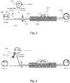
- a second spindle is provided, spaced apart from the first, for the winding of the substrate and deposited material onto a roll 202.
- the spindles are operated so as to unwind the substrate from the roll 201 and to rewind it onto roll 202 with the sphere dispersion coating 203 being coated on the substrate at a point between the rolls.
- a slot die 204 is located adjacent an upper surface of the substrate 200.
- the sphere dispersion described in association with step 100 of Figure 1 is provided to the upper surface of the substrate.
- relative movement between the substrate and the slot die is effected using a stationary die and a moving substrate.
- an aqueous coating 203 having a 50% content of solids (by weight) is delivered through the slot die to the substrate surface.
- a wet laydown density of about 20 gsm (grammes per square metre) is used (converting to about 10 gsm in a dried material).
- drier 205 Downstream of the slot die 204 and also positioned between the rollers is an elongate drier 205.
- the function of the drier is to remove the solvent in a controlled manner.
- the drying rate needs to be controlled so as to ensure the correct optical properties of the coating are obtained. Slow drying in a relatively low temperature environment using a long drier with minimal air turbulence is preferred.
- the coating is dried fully onto the substrate before rewinding onto the roll 202.
- the above described step provides for the general coating of the substrate. It is however also contemplated that, rather than coating the substrate evenly, the coating could be applied locally so as to produce resultant regions which might for example be arranged as indicia or images. Such regions might be applied using a moveable delivery head or other form of printing mechanism in place of the die 204.
- Step 120 Drying of sphere dispersion
- the carrier liquid In order to obtain a dry film of self-assembled microspheres, the carrier liquid must be driven off by a method such as heat, gas flow, infra-red radiation, ...
- the drying must be controlled, and slow enough to allow the spheres to orient themselves with respect to one another to give a self-assembled structure. "Slow” vs “rapid” drying are relative terms, and will depend on the particular solvent, additives, ...
- certain surfactants or surface-active molecules may result in a lower dispersion viscosity, or a lower degree of surface interactions between neighbouring spheres, which may result in more efficient self-assembly.
- co-solvents may be used to control the drying behaviour. For instance, high boiling solvents (such as ethylene glycol) may be added to the sphere dispersion. In this way, as the coating dries it may retain a greater amount of fluidity than provided by a pure water solvent, and therefore sphere mobility, allowing for more efficient self-assembly.
- lower-boiling additives may also be added (such as methanol). These lower-boiling additives may evaporate relatively rapidly, the fluid pressure of which may serve to orient or pre-orient the spheres into positions which may facilitate formation of the final self-assembled structure.
- the coating conditions may also be used to modify the self-assembly behaviour. For instance, drying at an increased temperature may result in poorer self-assembly due to kinetic trapping. However, instead of a hot-air dryer, one may employ a steam rehumidification unit (as used in the paper industry) to dry the sphere dispersion. In this case, the coating will be at a higher temperature, giving the spheres an increased mobility which may lead to a more efficient self-assembly. At the same time, the high concentration of water vapour would promote a longer drying process than if in dry conditions, which may prevent premature drying of the coating.
- a steam rehumidification unit as used in the paper industry
- the coated substrate may be wound into a roll for later processing as shown in Figure 2 , or may continue directly into the next process step.
- Such processing may in principle include the repeating of steps 110 and 120 so as to apply multiple coatings (which may also include microsphere compositions of the same or different composition or size). Such multiple passes may be used to produce indicia or images of different types.
- Step 130 Apply a curable resin and top substrate
- a top substrate is applied to the coating 203 by wet lamination of a curable resin.
- a curable resin such as a UV curable resin, electron-beam (EB) curable resin, thermal curable resin, .
- EB electron-beam
- a curable resin is coated onto the coating 203 of dried spheres using a coating method such as Gravure coating, forward or reverse, direct or indirect, Meyer rod, Slot die, Roll coaters (forward, reverse, multiroll), Multi-layer cascade(slide), Knife-over-roll, Curtain, Dip, Blade, Spray, Dahlgren, Screen printing, Extrusion, Comma Coating, Air Knife, Transfer, MICROGRAVURE®.
- FIG. 3 an analogous apparatus to that shown in Figure 2 is provided, with two separated rolls and a slot die. Specifically the roll 202 of substrate and coated spheres 203 is placed on a spindle and wound onto a roll 210 positioned downstream from the roll 202. A second slot die 211 (or offset gravure printing apparatus) positioned adjacent an upper exposed surface of the coating 203 just downstream from the roll 201 provides a further coating of UV curable resin 212 to the surface of coating 203.
- the curable resin may be provided as a substantially solvent-free coating (100% solids), or may be provided as a coating thinned with solvent, in which case the solvent would be required to be removed using a drying oven prior to lamination.
- a separate substrate is laminated onto the resin-coated microsphere film, forming a sandwich structure.
- This is achieved by providing further roll 213 of second substrate 214 material and laminating this material to the UV curable resin using nip rollers 215 (with an appropriate gap) positioned upon either side of the sandwich structure.
- the second substrate which is in this case a PET film of thickness 0.5 mil (-0.013mm) is pressed onto the UV curable resin as it passes through the nip of the rollers (the gap between them being about 2 mil ( ⁇ 0.05 mm).
- the substrate may consist of any of the substrates listed previously, preferably being a flexible substrate as in the present example. Ideally enough resin is applied to completely fill the space between the microspheres, with some excess resin overlayer. It is feasible to use excess, deficient, or stoichiometric quantities of resin.
- the typical structure resulting from this lamination consists of the original coating support substrate 200, followed by the resin-impregnated sphere coating 203, followed by a layer of excess resin, followed by the second substrate 214.
- Standard lamination parameters include nip gap, nip pressure, tension of substrates, temperature, roller diameter, material covering for either roller, amongst others.
- the curable resin may be coated onto a secondary substrate first, and this substrate subsequently laminated onto the microsphere coating (if the resin is diluted with solvent, the solvent is dried off prior to lamination). In this way, the resultant structure is the same, however by coating onto a bare substrate there may be some advantages in the coating process (coat weight control, uniformity, ...) than by coating onto a porous sphere layer.
- additives may be added to the resin, to change properties such as viscosity, rheology, and so on, as is known in the art.
- a relatively large excess of resin may be applied, such that following the curing step the excess resin on top of the sphere-resin composite may be thick/robust enough to serve as a self-supporting substrate in subsequent steps, thereby obviating the need for the separate additional substrate material 214.
- Curing is used to make the second substrate effective in fulfilling its intended roll in supporting the coating 203 and to lock the relative positions of the spheres. Curing may be achieved using any number of common curing methods, depending on the curing method (initiators, co-initiators, reactive groups, accelerators, kinetic modifiers, ...) used in the resin. Curing may be by using UV light (i.e. using a radical or cationic photoinitiator), IR radiation/heat (i.e. using a thermal free radical initiator), electron beam (which may be used initiator-free), gamma-rays (which may be used initiator-free), drying (i.e. evaporation of curing inhibitor such as amines) or other known curing methods.
- UV light i.e. using a radical or cationic photoinitiator
- IR radiation/heat i.e. using a thermal free radical initiator
- electron beam which may be used initiator-free
- gamma-rays which may be
- inerting such as nitrogen inerting
- FIG. 3 illustrates the UV curing apparatus according to the present example.
- a curing unit 216 is positioned downstream of the nip rollers 215.
- the UV curing unit may incorporate UV lamps, UV-LED arrays, or excimer flash lamps, for instance.
- the UV lamps may comprise highpressure mercury bulbs with atomic iron dopant (commonly known as a "D" bulb).
- the curing unit may also comprise means to eliminate waste heat produced by the UV lamps, such as chill rollers and air-impingement cooling.
- a UV lamp 217 is located within the drier 216 to expose the resin 212 to UV light thereby promoting the curing process. Note that, if used, the second substrate is sufficiently UV transparent to allow the curing to be performed.
- the UV curable resin is firstly coated upon the PET substrate (a similar substrate thickness may be used as described earlier) the resin is applied to the substrate using an offset gravure apparatus as shown at 218 in Figure 4 , this being adjacent the roll 213.
- the second slot die 211 is not required.
- the UV-curable resins we used are 100% solids (no solvent) and of relatively low viscosity (less than 100 cP (0.1 Pas)). It has been found in practice that the region where the UV exposure takes place should be cooled with a fan, compressed air or a nitrogen purge since if a high temperature is generated in the region then too much adhesion occurs making the delamination step (described below) difficult to perform.
- the laminate material may be wound into the roll 210 for later processing, or may continue directly into the next process step.
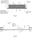
- Figure 5 is a schematic section through the sandwich structure showing the upper 214 and lower 200 PET substrates.
- An ordered array of silica spheres 230 can be seen to be in intimate contact with the lower PET substrate 200.
- the silica spheres are self-assembled into the array structure.
- Figure 5 is not to scale and in practice between 10 and 50 layers of spheres, more preferably between 15 and 30 layers of spheres are present.
- Figure 5 illustrates an important function of the UV curable resin in that it fully penetrates into the array structure, filling the voids between the silica spheres left by the earlier driving off of the solvent.
- the resin therefore provides the matrix of a silica-sphere:resin composite. This composite is labelled at 233.
- the refractive index of the resin and of course whichever gas fills the voids left by the removal of the spheres greatly influences the optical properties of the resultant photonic crystal structure.
- Figure 5 therefore shows a matrix region 231 of resin where the resin penetrates the sphere array.
- Figure 5 illustrates an excess resin region 232 providing a gap between the top of the array and the second substrate 214 above.
- the substrate 200 is removed from the "bottom" of the array to expose a contact surface of the photonic crystal structure.
- either the UV curable resin and/or the UV exposure could be applied in a patterned manner so as to ultimately provide the resultant photonic crystal material in the shape of indicia or as an image.
- Step 150 Substrate stripping - Delamination
- the ordered layer of spheres in the coating 203 is sandwiched between two substrates. This sandwich structure is then peeled apart.
- the first substrate 200 is mechanically peeled off and discarded, while both the sphere-resin composite 233 and excess resin 232 overlayer may remain on the second substrate.
- the second substrate 214 may be peeled off and carry with it the excess cured resin layer.
- the removal of the first substrate 200 exposes the bottom of the sphere array
- the removal of the substrate 214 and resin overlayer 232 exposes the top of the sphere array. Exposing the large top or bottom interface of the array allows the entire sphere array to be etched rapidly and homogenously using an etchant. Even a very thin film (i.e. less than 50 nm) of cured resin remaining on the surface to be etched may adversely impact the etching time required, in addition to impacting the visual effect of the final coating.
- FIG 6 again there is a similar basic arrangement provided of winding a web between an "unwinding” and “rewinding” roll.
- the roll 210 from Figure 3 is provided on a spindle.
- a second spindle holds a roll 240 and the sandwich structure is wound from the roll 210 to the roll 240.
- a PTFE stripping bar 241 is located at a position between the rolls. This traverses the direction of travel of the sandwich structure.
- a downstream edge of the bar which faces roll 240 and which lies in a parallel plane to the upper surface of the sandwich structure is used to remove the first substrate 200. It should be noted therefore that the orientation of the roll 210 is reversed in the vertical direction in comparison with Figure 3 .
- the substrate surface 200 gently slides across a downward facing surface of the bar (this being aided by the use of the PTFE material). At the downstream edge of this surface is positioned the edge discussed above.
- the substrate 200 undergoes a rapid change of direction at a high take off "peeling" angle in order to effect clean peeling from the composite structure 233 and in particular the flat surface (originally lower surface) of the array of spheres and matrix. It has been shown that a high peeling angle of close to 180 degrees provides excellent results.
- the peeling angle is shown in Figure 6 at 242.
- a support roller 243 is provided beneath the stripping bar to ensure that the sandwich structure is urged against the bar.
- the removed substrate is wound onto a further roll 243 which is discarded.
- the remainder of the sandwich structure continues to the roll 240 where is it wound for further use.
- the structure may continue to the next stage of processing without winding.
- the surfaces of both the first and second substrates will strongly influence their adhesion to the resin or sphere-resin composite.
- the first substrate 200 should have at least satisfactory adhesion to the sphere coating (see Figure 2 ), as well as to the cured sphere-resin composite 233 formed later, to allow for roll-to-roll processing.
- Substrates may be treated by any number of surface treatments known in the art such as corona discharge, plasma, flame, or chemical modification.
- the nature of the substrate may be selected from a wealth of commercially-available substrates with or without surface modifications such as gel-coats, tie-coats, release coatings, adhesion promoters, etc... It may be preferable for the second substrate to have greater surface interaction with the resin to facilitate transfer thereon.
- the Figure 6 example described above causes the removal of the first substrate.
- the second substrate which is removed.
- either of the substrates is peeled off, it can be done at a variety of angles, ranging from close to 0 degrees up to 180 degrees, assuming the other substrate is held flat and depending upon the application.
- both substrates may be peeled at an angle, with neither in plane with the original laminate.
- a system of rollers with separator bars may be used to more effectively carry out the delamination.
- the greater the curvature at which this substrate is peeled (relative to its original orientation), the higher the propensity for it to detach from the layer immediately under it.
- the underlying aim of the method is to provide an improved and industrially applicable means for generating inverse opal photonic crystal structures.
- a crucial aspect of this is in providing multiple paths into the structure to allow the removal agent (such as etchant) to remove the sphere material.
- the use of the peeling step in combination with the substrates provides a surface which is smooth and which may be attacked readily by the agent.
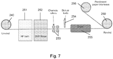
- FIG. 7 the apparatus used for etching of the material of the present example is now described.
- the unwinding roll of Figure 7 is shown at 240 (as referred to in Figure 6 ) and the eventual rewinding roll is shown at 250.
- Downstream of the roll 240 is provided an etchant bath 251 containing aqueous hydrofluoric acid.
- the cured microsphere-polymer composite film is dipped in the aqueous solution of hydrofluoric acid (HF).
- HF hydrofluoric acid
- the concentration of the etchant may range from 0.1% to 70%, being most preferably in the range of 2% to 20%. Etching times may range from 0.1 seconds to 5 minutes, depending on the HF concentration and characteristics of the material. Typically a 6 to 12% HF (aq) solution with a dwell time in the etchant of 15 to 5 seconds (respectively) is used in this example. Downstream of the etchant bath 251 a wash bath 252 is located for receiving and washing the etched structure. Alternatively or in addition, washing may be carried out using a spray of wash fluid.
- Washing may also be carried out in multiple stages, for instance with an initial pre-wash bath to remove the majority of the etchant and by-products, followed by a second wash with a bath/spray of pure water.
- the wash station contains de-ionised water for removing the etchant.
- Systems for continuous etching with aqueous acids (such as HF) using moving bath immersion are available, for instance, from suppliers such as Infinity Precision Systems LLC of Minneapolis, USA.
- the structure may be passed through pairs of drying rollers 253 (chamois or equivalent surface material, may also alternately comprise elastomeric squeegees) for drying each side of the structure and then on past a slot air knife 254 which provides intensive drying of at least the etched surface of the material. Alternately, the use of one of more slot air knives may be sufficient to eliminate excess wash liquid without the need for drying rollers or squeegees.
- a final dryer 255 which is used to remove all of the excess liquid from the structure and minimises the liquid remaining within the interlinked spherical-shaped voids within the structure.
- a typical temperature used for the final drying step is 90 to 120 Celsius.
- the substrate On emerging from the dryer, the substrate, bearing its etched material, is wound on to the roll 250. Due to the delicate nature of the structure the material may be co-wound with a parchment paper interleave layer which is supplied from a further roll 256. This may also act as a release layer for later use of the material.
- etching of silica spheres may be effected by vapour-phase etching, whereby gaseous HF reacts with the silica (SiO 2 ) to produce SiF 4 and H 2 O vapours.
- the binder used in the sphere coating may dissolve in the etchant.
- the binder may mostly dissolve, but leave behind a layer adhered to the porous polymer.
- the binder may either swell but not dissolve, or remain mainly unaffected by the etchant. Where the binder is unaffected, flow paths must exist within or adjacent the binder to allow the etchant to penetrate the spheres.
- sphere type will dictate the etching conditions.
- spheres may be formed from other metal oxides with different etching chemistry (TiO 2 - strong base; Fe 2 O 3 - HCI; etc%), or polymers (i.e. PMMA, PS, ...) which may be etched by various organic solvents.
- the sphere size may affect the etching times required, for instance larger sphere sizes may etch relatively slower than smaller spheres due to a lower surface-volume ratio.
- sphere size may affect the relative size of the contact points between spheres, which in turn would influence the size of the hole dividing two neighbouring spherical cavities in the resulting porous polymer. This may then influence the permeation of the etchant throughout the structure, whereby larger through-holes may result in relatively higher diffusion rates of etchant and thereby to larger etch rates of the sphere array.
- the type of binder and its thickness may impact the permeation of the etchant throughout the structure, thereby influencing etch rate and homogeneity.
- the etchant concentration, temperature, mass flow, by-product removal/buildup, additives may all influence the rate, extent, and homogeneity of etching.
- indicia or images could be produced in the final photonic crystal material by the selective application of the etchant, for example using a printing technique.
- Step 170 Use of the material
- Example articles include security devices for use in security documents such as banknotes, cheques, passports, identity cards, certificates of authenticity, fiscal stamps and other documents for securing value or personal identity.
- the present method allows the generation of substantial quantities of inverse opal photonic crystal material having high quality optical properties.
- the present method provides significant advantages by introducing a second substrate prior to polymerization, thus allowing the "automatic" exposure of a high quality surface to be etched. This obviates the step of excess polymer removal that is required in known processes and which is very difficult to perform industrially.
- the second substrate supports the resulting photonic crystal film during etching, in contrast with the prior technique of releasing a fragile membrane to float freely.
- the use of such a second substrate may be readily implemented in an industrial context, whereas the use of a free floating structure would present substantial technical challenges.
Landscapes
- Physics & Mathematics (AREA)
- Chemical & Material Sciences (AREA)
- Engineering & Computer Science (AREA)
- Optics & Photonics (AREA)
- Nanotechnology (AREA)
- General Physics & Mathematics (AREA)
- Crystallography & Structural Chemistry (AREA)
- Manufacturing & Machinery (AREA)
- Life Sciences & Earth Sciences (AREA)
- Biophysics (AREA)
- Microelectronics & Electronic Packaging (AREA)
- Business, Economics & Management (AREA)
- Finance (AREA)
- Accounting & Taxation (AREA)
- Materials Engineering (AREA)
- Health & Medical Sciences (AREA)
- Chemical Kinetics & Catalysis (AREA)
- Medicinal Chemistry (AREA)
- Polymers & Plastics (AREA)
- Organic Chemistry (AREA)
- Application Of Or Painting With Fluid Materials (AREA)
Claims (20)
- Procédé de formation d'un matériau à cristaux photoniques ayant une structure d'opale inverse, comprenant :a) la production d'un réseau de particules sur un premier substrat, le réseau contenant des interstices entre les particules destinés à la réception d'un matériau de matrice ;b) la liaison des particules les unes aux autres de manière à fixer les positions relatives des particules les unes par rapport aux autres ;c) l'utilisation d'un matériau de matrice pour combler au moins en partie les interstices ;d) la fixation d'un second substrat au réseau, ou la formation d'un second substrat sur le réseau, de sorte que le réseau soit positionné entre les premier et second substrats ;e) la fixation de la position du matériau de matrice par rapport aux particules ;f) le détachement d'au moins un des premier ou second substrats du réseau de manière à exposer une surface respective de contact du réseau ; et,g) l'application d'un agent d'attaque chimique à la surface de contact, ledit agent d'attaque chimique étant conçu pour éliminer du matériau des particules de manière à former la structure d'opale inverse.
- Procédé selon la revendication 1, dans lequel l'étape (b) se fait à l'aide d'un liant.
- Procédé selon la revendication 2, dans lequel ledit matériau de liant est présent lors de l'étape (a) et dans les conditions de procédé concernant l'étape (a), a une fonction de production d'une liaison insuffisante entre les particules de manière à permettre aux particules de s'assembler automatiquement sous la forme dudit réseau.
- Procédé selon la revendication 2 ou la revendication 3, dans lequel le liant est disposé pour lier le réseau au premier substrat d'une manière détachable de manière à permettre la réalisation de l'étape (g).
- Procédé selon l'une quelconque des revendications précédentes, dans lequel ladite surface de contact du réseau est une surface sensiblement plane.
- Procédé selon l'une quelconque des revendications précédentes, dans lequel ladite surface de contact du réseau comprend de nombreuses voies à travers lesquelles l'agent d'attaque chimique peut pénétrer dans le réseau soit directement par contact avec les particules, soit à travers le liant.
- Procédé selon la revendication 6, dans lequel la surface de contact comprend soit sensiblement aucun matériau liant soit au moins une région de matériau de liant présentant une épaisseur inférieure à 50 nm.
- Procédé selon l'une quelconque des revendications précédentes, dans lequel l'étape (d) a lieu avant l'étape (c).
- Procédé selon la revendication 8, dans lequel le matériau de matrice est attaché au substrat avant l'étape (c).
- Procédé selon l'une quelconque des revendications précédentes, dans lequel l'étape (f) a lieu selon un procédé de pelage dans lequel le réseau et la matrice sont conjointement séparés du substrat selon un angle prédéfini.
- Procédé selon la revendication 10, dans lequel le pelage a lieu à l'aide d'une combinaison d'un ou de plusieurs des rouleaux et des barres séparatrices.
- Procédé selon l'une quelconque des revendications précédentes, dans lequel le second substrat de l'étape (d) est produit à partir de la matrice de l'étape (c) de sorte que la matrice forme un substrat autoporteur.
- Procédé selon l'une quelconque des revendications précédentes, dans lequel à l'étape (g), l'agent d'attaque chimique est appliqué par au moins une méthode parmi les suivantes :i) trempage du réseau et de la matrice dans un bain contenant l'agent d'attaque chimique ;ii) pulvérisation de l'agent d'attaque chimique sur la surface de contact ;iii) utilisation de l'agent d'attaque sous forme de vapeur sur la surface de contact, de manière à effectuer une attaque chimique en phase gazeuse.
- Procédé selon la revendication 13, dans lequel un flux de l'agent d'attaque chimique est appliqué à la surface de contact de manière à éliminer les sous-produits du processus d'attaque chimique.
- Procédé selon la revendication 14, dans lequel un flux de l'agent d'attaque chimique est appliqué sensiblement à l'ensemble de la surface de contact simultanément.
- Procédé selon l'une quelconque des revendications précédentes, comprenant en outre la réalisation d'au moins une étape (a) à (g) par enroulement du matériau cristallin photonique qui est formé d'un premier rouleau sur au moins un second rouleau.
- Procédé selon la revendication 16, dans lequel le matériau cristallin photonique est mis en suspension entre lesdits rouleaux pendant ladite au moins une étape.
- Procédé selon la revendication 16 ou la revendication 17, comprenant en outre l'application d'un processus de séchage en tant que partie d'au moins une étape (a) à (e) ou (g).
- Procédé selon l'une quelconque des revendications précédentes, dans lequel au moins une desdites substances est formée d'un film fin de poly(téréphtalate d'éthylène) sur lequel est disposé un réseau de particules de silice dans une résine durcissable aux UV, lesdites particules étant éliminées grâce à une solution d'acide fluorhydrique en tant qu'agent d'attaque chimique.
- Procédé selon l'une quelconque des revendications précédentes, comprenant en outre l'incorporation du matériau cristallin photonique dans un dispositif de sécurité.
Applications Claiming Priority (2)
| Application Number | Priority Date | Filing Date | Title |
|---|---|---|---|
| GB1216318.4A GB2505895B (en) | 2012-09-13 | 2012-09-13 | Method for forming photonic crystal materials |
| PCT/GB2013/052396 WO2014041360A1 (fr) | 2012-09-13 | 2013-09-13 | Procédé de formation de matières à cristaux photoniques |
Publications (2)
| Publication Number | Publication Date |
|---|---|
| EP2895899A1 EP2895899A1 (fr) | 2015-07-22 |
| EP2895899B1 true EP2895899B1 (fr) | 2018-08-15 |
Family
ID=47137366
Family Applications (1)
| Application Number | Title | Priority Date | Filing Date |
|---|---|---|---|
| EP13763287.3A Not-in-force EP2895899B1 (fr) | 2012-09-13 | 2013-09-13 | Procédé de formation de matières à cristaux photoniques |
Country Status (4)
| Country | Link |
|---|---|
| EP (1) | EP2895899B1 (fr) |
| CA (1) | CA2884809C (fr) |
| GB (1) | GB2505895B (fr) |
| WO (1) | WO2014041360A1 (fr) |
Families Citing this family (7)
| Publication number | Priority date | Publication date | Assignee | Title |
|---|---|---|---|---|
| CN105019057B (zh) * | 2015-07-09 | 2017-06-13 | 南通纺织丝绸产业技术研究院 | 反蛋白石胶体晶体纤维的制备方法 |
| DE102018101109A1 (de) | 2018-01-18 | 2019-07-18 | Mitsubishi Hitec Paper Europe Gmbh | Wärmeempfindliches Aufzeichnungsmaterial umfassend eine Mehrzahl von Submikrometerpartikeln mit monomodaler Partikelgrößenverteilung |
| US20200281531A1 (en) * | 2019-03-07 | 2020-09-10 | City University Of Hong Kong | Electromedical apparatus, a method for manufacturing the electromedical apparatus and a method for deploying the electromedical apparatus |
| CN111751525A (zh) * | 2020-06-18 | 2020-10-09 | 东南大学 | 一种基于有序微纳结构的侧向流免疫试纸条 |
| KR102495255B1 (ko) * | 2020-08-11 | 2023-02-02 | 한국조폐공사 | 광결정 필름 제조 장치 및 제조 방법 |
| CN113782061B (zh) * | 2021-07-23 | 2022-11-08 | 深圳大学 | 一种润湿响应的光学信息加密薄层及其制备方法 |
| CN115354511B (zh) * | 2022-08-09 | 2024-07-09 | 浙江理工大学 | 一种立体印花面料及其制备方法 |
Family Cites Families (14)
| Publication number | Priority date | Publication date | Assignee | Title |
|---|---|---|---|---|
| US6858079B2 (en) * | 2000-11-28 | 2005-02-22 | Nec Laboratories America, Inc. | Self-assembled photonic crystals and methods for manufacturing same |
| US20040071965A1 (en) * | 2000-11-30 | 2004-04-15 | Guoyi Fu | Particles with opalescent effect |
| JP2004117456A (ja) * | 2002-09-24 | 2004-04-15 | Ricoh Co Ltd | 微粒子構造体の製造方法 |
| US7106938B2 (en) * | 2004-03-16 | 2006-09-12 | Regents Of The University Of Minnesota | Self assembled three-dimensional photonic crystal |
| JP2006167855A (ja) * | 2004-12-15 | 2006-06-29 | Ricoh Co Ltd | 周期性構造物の作成方法、周期性構造物、および、周期性構造物を用いた光学素子 |
| US7794538B2 (en) * | 2005-02-02 | 2010-09-14 | Robert A Marshall | Self-assembly method, opal, photonic band gap, and light source |
| US7687372B2 (en) * | 2005-04-08 | 2010-03-30 | Versatilis Llc | System and method for manufacturing thick and thin film devices using a donee layer cleaved from a crystalline donor |
| KR100764826B1 (ko) * | 2006-07-05 | 2007-10-08 | 한국과학기술원 | 반사형 표시소자 및 광도파로의 응용을 위한 픽셀화된 광결정 필름 및 그의 제조방법 |
| AU2007346889B2 (en) * | 2007-02-16 | 2014-05-15 | Opalux Incorporated | Compressible photonic crystal |
| WO2010027854A1 (fr) * | 2008-08-26 | 2010-03-11 | President And Fellows Of Harvard College | Films poreux obtenus selon un procédé de co-assemblage et de formation de matrice |
| CN101428493B (zh) * | 2008-12-12 | 2011-08-17 | 清华大学 | 一种在疏水性衬底上制备聚合物胶体晶体薄膜的方法 |
| GB0911792D0 (en) * | 2009-07-07 | 2009-08-19 | Rue De Int Ltd | Photonic crystal material |
| CA2819336C (fr) * | 2010-11-29 | 2019-03-12 | President And Fellows Of Harvard College | Manipulation de fluides dans des structures photoniques poreuses tridimensionnelles ayant des proprietes de surface comprenant des motifs |
| US9733393B2 (en) * | 2011-02-24 | 2017-08-15 | National University Of Singapore | Light-reflective structures and methods for their manufacture and use |
-
2012
- 2012-09-13 GB GB1216318.4A patent/GB2505895B/en not_active Expired - Fee Related
-
2013
- 2013-09-13 WO PCT/GB2013/052396 patent/WO2014041360A1/fr not_active Ceased
- 2013-09-13 CA CA2884809A patent/CA2884809C/fr active Active
- 2013-09-13 EP EP13763287.3A patent/EP2895899B1/fr not_active Not-in-force
Non-Patent Citations (1)
| Title |
|---|
| None * |
Also Published As
| Publication number | Publication date |
|---|---|
| EP2895899A1 (fr) | 2015-07-22 |
| CA2884809A1 (fr) | 2014-03-20 |
| GB201216318D0 (en) | 2012-10-24 |
| GB2505895B (en) | 2018-03-21 |
| WO2014041360A1 (fr) | 2014-03-20 |
| CA2884809C (fr) | 2021-05-11 |
| GB2505895A (en) | 2014-03-19 |
Similar Documents
| Publication | Publication Date | Title |
|---|---|---|
| EP2895899B1 (fr) | Procédé de formation de matières à cristaux photoniques | |
| KR101238769B1 (ko) | 발수성막, 발수성 및 친수성의 영역을 갖는 패턴화막, 및 그 제조 방법 | |
| EP1479734B1 (fr) | Procede de preparation d'un revetement de surface nanostructure, revetements nanostructures et articles contenant le revetement | |
| CN112513686A (zh) | 高透射率光控膜 | |
| WO2012077738A1 (fr) | Stratifié à structure fine, procédé de préparation d'un stratifié à structure fine et procédé de production d'un stratifié à structure fine | |
| TW201519962A (zh) | 用於在帶狀薄膜基材上形成具有不連續圖案之塗膜的塗敷裝置、及具有凹凸圖案之帶狀薄膜構件的製造方法 | |
| JP2015500515A (ja) | 反射型偏光板 | |
| JP2013531808A (ja) | 基板のハイスループット、ミクロンスケールエッチングのためのステンシルならびにその製造方法および使用方法 | |
| CN109476119B (zh) | 光学层叠体的制造方法、以及光学层叠体中间体 | |
| KR20160137632A (ko) | 편광 방사 디바이스 | |
| US20130078796A1 (en) | Process for making a patterned metal oxide structure | |
| CN108602242B (zh) | 3-d印刷表面 | |
| CN106104324B (zh) | 偏光板的制造方法 | |
| EP1789482B1 (fr) | Procede de production de film | |
| JP2007004155A (ja) | 反射防止膜及びその製造方法 | |
| WO2009128591A1 (fr) | Procédé de formation de motif de cristaux photoniques hémisphériques et fabrication de cristaux photoniques de diverses formes à l'aide de suspensions colloïdales pouvant photodurcir | |
| JP2012223702A (ja) | 塗工膜の乾燥方法及び積層体製造システム | |
| JP6393479B2 (ja) | 親水性積層体、及びその製造方法、並びに物品、及びその製造方法 | |
| JP2009167315A (ja) | 多孔質体の製造方法 | |
| Oh et al. | Surface morphology and transparency control of a metal/PDMS layered substrate by stretching | |
| Uddin et al. | Materials and process optimization in the reliable fabrication of polymer photonic devices | |
| JP2013071118A (ja) | 超親水性の表面領域を有する塗膜、及びその製造方法 | |
| CN203012350U (zh) | 微细凹凸图案基材、模具以及线栅偏振片 | |
| JP5116256B2 (ja) | ハニカム複合膜及びその製造方法 | |
| JP5260578B2 (ja) | 積層フィルムの塗布方法 |
Legal Events
| Date | Code | Title | Description |
|---|---|---|---|
| PUAI | Public reference made under article 153(3) epc to a published international application that has entered the european phase |
Free format text: ORIGINAL CODE: 0009012 |
|
| 17P | Request for examination filed |
Effective date: 20150409 |
|
| AK | Designated contracting states |
Kind code of ref document: A1 Designated state(s): AL AT BE BG CH CY CZ DE DK EE ES FI FR GB GR HR HU IE IS IT LI LT LU LV MC MK MT NL NO PL PT RO RS SE SI SK SM TR |
|
| AX | Request for extension of the european patent |
Extension state: BA ME |
|
| DAX | Request for extension of the european patent (deleted) | ||
| GRAP | Despatch of communication of intention to grant a patent |
Free format text: ORIGINAL CODE: EPIDOSNIGR1 |
|
| INTG | Intention to grant announced |
Effective date: 20180308 |
|
| GRAS | Grant fee paid |
Free format text: ORIGINAL CODE: EPIDOSNIGR3 |
|
| GRAA | (expected) grant |
Free format text: ORIGINAL CODE: 0009210 |
|
| AK | Designated contracting states |
Kind code of ref document: B1 Designated state(s): AL AT BE BG CH CY CZ DE DK EE ES FI FR GB GR HR HU IE IS IT LI LT LU LV MC MK MT NL NO PL PT RO RS SE SI SK SM TR |
|
| REG | Reference to a national code |
Ref country code: CH Ref legal event code: EP Ref country code: GB Ref legal event code: FG4D Ref country code: AT Ref legal event code: REF Ref document number: 1030440 Country of ref document: AT Kind code of ref document: T Effective date: 20180815 |
|
| REG | Reference to a national code |
Ref country code: IE Ref legal event code: FG4D |
|
| REG | Reference to a national code |
Ref country code: DE Ref legal event code: R096 Ref document number: 602013042049 Country of ref document: DE |
|
| REG | Reference to a national code |
Ref country code: NL Ref legal event code: MP Effective date: 20180815 |
|
| REG | Reference to a national code |
Ref country code: LT Ref legal event code: MG4D |
|
| REG | Reference to a national code |
Ref country code: AT Ref legal event code: MK05 Ref document number: 1030440 Country of ref document: AT Kind code of ref document: T Effective date: 20180815 |
|
| PG25 | Lapsed in a contracting state [announced via postgrant information from national office to epo] |
Ref country code: LT Free format text: LAPSE BECAUSE OF FAILURE TO SUBMIT A TRANSLATION OF THE DESCRIPTION OR TO PAY THE FEE WITHIN THE PRESCRIBED TIME-LIMIT Effective date: 20180815 Ref country code: FI Free format text: LAPSE BECAUSE OF FAILURE TO SUBMIT A TRANSLATION OF THE DESCRIPTION OR TO PAY THE FEE WITHIN THE PRESCRIBED TIME-LIMIT Effective date: 20180815 Ref country code: RS Free format text: LAPSE BECAUSE OF FAILURE TO SUBMIT A TRANSLATION OF THE DESCRIPTION OR TO PAY THE FEE WITHIN THE PRESCRIBED TIME-LIMIT Effective date: 20180815 Ref country code: IS Free format text: LAPSE BECAUSE OF FAILURE TO SUBMIT A TRANSLATION OF THE DESCRIPTION OR TO PAY THE FEE WITHIN THE PRESCRIBED TIME-LIMIT Effective date: 20181215 Ref country code: BG Free format text: LAPSE BECAUSE OF FAILURE TO SUBMIT A TRANSLATION OF THE DESCRIPTION OR TO PAY THE FEE WITHIN THE PRESCRIBED TIME-LIMIT Effective date: 20181115 Ref country code: NL Free format text: LAPSE BECAUSE OF FAILURE TO SUBMIT A TRANSLATION OF THE DESCRIPTION OR TO PAY THE FEE WITHIN THE PRESCRIBED TIME-LIMIT Effective date: 20180815 Ref country code: AT Free format text: LAPSE BECAUSE OF FAILURE TO SUBMIT A TRANSLATION OF THE DESCRIPTION OR TO PAY THE FEE WITHIN THE PRESCRIBED TIME-LIMIT Effective date: 20180815 Ref country code: GR Free format text: LAPSE BECAUSE OF FAILURE TO SUBMIT A TRANSLATION OF THE DESCRIPTION OR TO PAY THE FEE WITHIN THE PRESCRIBED TIME-LIMIT Effective date: 20181116 Ref country code: NO Free format text: LAPSE BECAUSE OF FAILURE TO SUBMIT A TRANSLATION OF THE DESCRIPTION OR TO PAY THE FEE WITHIN THE PRESCRIBED TIME-LIMIT Effective date: 20181115 Ref country code: SE Free format text: LAPSE BECAUSE OF FAILURE TO SUBMIT A TRANSLATION OF THE DESCRIPTION OR TO PAY THE FEE WITHIN THE PRESCRIBED TIME-LIMIT Effective date: 20180815 |
|
| PG25 | Lapsed in a contracting state [announced via postgrant information from national office to epo] |
Ref country code: AL Free format text: LAPSE BECAUSE OF FAILURE TO SUBMIT A TRANSLATION OF THE DESCRIPTION OR TO PAY THE FEE WITHIN THE PRESCRIBED TIME-LIMIT Effective date: 20180815 Ref country code: LV Free format text: LAPSE BECAUSE OF FAILURE TO SUBMIT A TRANSLATION OF THE DESCRIPTION OR TO PAY THE FEE WITHIN THE PRESCRIBED TIME-LIMIT Effective date: 20180815 Ref country code: HR Free format text: LAPSE BECAUSE OF FAILURE TO SUBMIT A TRANSLATION OF THE DESCRIPTION OR TO PAY THE FEE WITHIN THE PRESCRIBED TIME-LIMIT Effective date: 20180815 |
|
| PG25 | Lapsed in a contracting state [announced via postgrant information from national office to epo] |
Ref country code: EE Free format text: LAPSE BECAUSE OF FAILURE TO SUBMIT A TRANSLATION OF THE DESCRIPTION OR TO PAY THE FEE WITHIN THE PRESCRIBED TIME-LIMIT Effective date: 20180815 Ref country code: PL Free format text: LAPSE BECAUSE OF FAILURE TO SUBMIT A TRANSLATION OF THE DESCRIPTION OR TO PAY THE FEE WITHIN THE PRESCRIBED TIME-LIMIT Effective date: 20180815 Ref country code: ES Free format text: LAPSE BECAUSE OF FAILURE TO SUBMIT A TRANSLATION OF THE DESCRIPTION OR TO PAY THE FEE WITHIN THE PRESCRIBED TIME-LIMIT Effective date: 20180815 Ref country code: RO Free format text: LAPSE BECAUSE OF FAILURE TO SUBMIT A TRANSLATION OF THE DESCRIPTION OR TO PAY THE FEE WITHIN THE PRESCRIBED TIME-LIMIT Effective date: 20180815 Ref country code: CZ Free format text: LAPSE BECAUSE OF FAILURE TO SUBMIT A TRANSLATION OF THE DESCRIPTION OR TO PAY THE FEE WITHIN THE PRESCRIBED TIME-LIMIT Effective date: 20180815 |
|
| REG | Reference to a national code |
Ref country code: DE Ref legal event code: R097 Ref document number: 602013042049 Country of ref document: DE |
|
| PG25 | Lapsed in a contracting state [announced via postgrant information from national office to epo] |
Ref country code: SM Free format text: LAPSE BECAUSE OF FAILURE TO SUBMIT A TRANSLATION OF THE DESCRIPTION OR TO PAY THE FEE WITHIN THE PRESCRIBED TIME-LIMIT Effective date: 20180815 Ref country code: DK Free format text: LAPSE BECAUSE OF FAILURE TO SUBMIT A TRANSLATION OF THE DESCRIPTION OR TO PAY THE FEE WITHIN THE PRESCRIBED TIME-LIMIT Effective date: 20180815 Ref country code: SK Free format text: LAPSE BECAUSE OF FAILURE TO SUBMIT A TRANSLATION OF THE DESCRIPTION OR TO PAY THE FEE WITHIN THE PRESCRIBED TIME-LIMIT Effective date: 20180815 |
|
| REG | Reference to a national code |
Ref country code: BE Ref legal event code: MM Effective date: 20180930 |
|
| PLBE | No opposition filed within time limit |
Free format text: ORIGINAL CODE: 0009261 |
|
| STAA | Information on the status of an ep patent application or granted ep patent |
Free format text: STATUS: NO OPPOSITION FILED WITHIN TIME LIMIT |
|
| REG | Reference to a national code |
Ref country code: IE Ref legal event code: MM4A |
|
| PG25 | Lapsed in a contracting state [announced via postgrant information from national office to epo] |
Ref country code: MC Free format text: LAPSE BECAUSE OF FAILURE TO SUBMIT A TRANSLATION OF THE DESCRIPTION OR TO PAY THE FEE WITHIN THE PRESCRIBED TIME-LIMIT Effective date: 20180815 Ref country code: LU Free format text: LAPSE BECAUSE OF NON-PAYMENT OF DUE FEES Effective date: 20180913 |
|
| 26N | No opposition filed |
Effective date: 20190516 |
|
| PG25 | Lapsed in a contracting state [announced via postgrant information from national office to epo] |
Ref country code: IE Free format text: LAPSE BECAUSE OF NON-PAYMENT OF DUE FEES Effective date: 20180913 |
|
| PG25 | Lapsed in a contracting state [announced via postgrant information from national office to epo] |
Ref country code: BE Free format text: LAPSE BECAUSE OF NON-PAYMENT OF DUE FEES Effective date: 20180930 Ref country code: SI Free format text: LAPSE BECAUSE OF FAILURE TO SUBMIT A TRANSLATION OF THE DESCRIPTION OR TO PAY THE FEE WITHIN THE PRESCRIBED TIME-LIMIT Effective date: 20180815 |
|
| PGFP | Annual fee paid to national office [announced via postgrant information from national office to epo] |
Ref country code: IT Payment date: 20190917 Year of fee payment: 7 |
|
| PG25 | Lapsed in a contracting state [announced via postgrant information from national office to epo] |
Ref country code: MT Free format text: LAPSE BECAUSE OF NON-PAYMENT OF DUE FEES Effective date: 20180913 |
|
| PGFP | Annual fee paid to national office [announced via postgrant information from national office to epo] |
Ref country code: CH Payment date: 20190913 Year of fee payment: 7 |
|
| PG25 | Lapsed in a contracting state [announced via postgrant information from national office to epo] |
Ref country code: TR Free format text: LAPSE BECAUSE OF FAILURE TO SUBMIT A TRANSLATION OF THE DESCRIPTION OR TO PAY THE FEE WITHIN THE PRESCRIBED TIME-LIMIT Effective date: 20180815 |
|
| PG25 | Lapsed in a contracting state [announced via postgrant information from national office to epo] |
Ref country code: PT Free format text: LAPSE BECAUSE OF FAILURE TO SUBMIT A TRANSLATION OF THE DESCRIPTION OR TO PAY THE FEE WITHIN THE PRESCRIBED TIME-LIMIT Effective date: 20180815 |
|
| PG25 | Lapsed in a contracting state [announced via postgrant information from national office to epo] |
Ref country code: MK Free format text: LAPSE BECAUSE OF NON-PAYMENT OF DUE FEES Effective date: 20180815 Ref country code: CY Free format text: LAPSE BECAUSE OF FAILURE TO SUBMIT A TRANSLATION OF THE DESCRIPTION OR TO PAY THE FEE WITHIN THE PRESCRIBED TIME-LIMIT Effective date: 20180815 Ref country code: HU Free format text: LAPSE BECAUSE OF FAILURE TO SUBMIT A TRANSLATION OF THE DESCRIPTION OR TO PAY THE FEE WITHIN THE PRESCRIBED TIME-LIMIT; INVALID AB INITIO Effective date: 20130913 |
|
| REG | Reference to a national code |
Ref country code: CH Ref legal event code: PL |
|
| PG25 | Lapsed in a contracting state [announced via postgrant information from national office to epo] |
Ref country code: LI Free format text: LAPSE BECAUSE OF NON-PAYMENT OF DUE FEES Effective date: 20200930 Ref country code: CH Free format text: LAPSE BECAUSE OF NON-PAYMENT OF DUE FEES Effective date: 20200930 |
|
| PG25 | Lapsed in a contracting state [announced via postgrant information from national office to epo] |
Ref country code: IT Free format text: LAPSE BECAUSE OF NON-PAYMENT OF DUE FEES Effective date: 20200913 |
|
| PGFP | Annual fee paid to national office [announced via postgrant information from national office to epo] |
Ref country code: GB Payment date: 20220721 Year of fee payment: 10 Ref country code: DE Payment date: 20220609 Year of fee payment: 10 |
|
| PGFP | Annual fee paid to national office [announced via postgrant information from national office to epo] |
Ref country code: FR Payment date: 20220709 Year of fee payment: 10 |
|
| REG | Reference to a national code |
Ref country code: DE Ref legal event code: R119 Ref document number: 602013042049 Country of ref document: DE |
|
| GBPC | Gb: european patent ceased through non-payment of renewal fee |
Effective date: 20230913 |
|
| PG25 | Lapsed in a contracting state [announced via postgrant information from national office to epo] |
Ref country code: GB Free format text: LAPSE BECAUSE OF NON-PAYMENT OF DUE FEES Effective date: 20230913 |
|
| PG25 | Lapsed in a contracting state [announced via postgrant information from national office to epo] |
Ref country code: GB Free format text: LAPSE BECAUSE OF NON-PAYMENT OF DUE FEES Effective date: 20230913 Ref country code: FR Free format text: LAPSE BECAUSE OF NON-PAYMENT OF DUE FEES Effective date: 20230930 Ref country code: DE Free format text: LAPSE BECAUSE OF NON-PAYMENT OF DUE FEES Effective date: 20240403 |