EP2890217A1 - Control device for induction heating units - Google Patents
Control device for induction heating units Download PDFInfo
- Publication number
- EP2890217A1 EP2890217A1 EP12883809.1A EP12883809A EP2890217A1 EP 2890217 A1 EP2890217 A1 EP 2890217A1 EP 12883809 A EP12883809 A EP 12883809A EP 2890217 A1 EP2890217 A1 EP 2890217A1
- Authority
- EP
- European Patent Office
- Prior art keywords
- slave
- master
- inverter
- phase
- voltage
- Prior art date
- Legal status (The legal status is an assumption and is not a legal conclusion. Google has not performed a legal analysis and makes no representation as to the accuracy of the status listed.)
- Granted
Links
Images






Classifications
-
- H—ELECTRICITY
- H05—ELECTRIC TECHNIQUES NOT OTHERWISE PROVIDED FOR
- H05B—ELECTRIC HEATING; ELECTRIC LIGHT SOURCES NOT OTHERWISE PROVIDED FOR; CIRCUIT ARRANGEMENTS FOR ELECTRIC LIGHT SOURCES, IN GENERAL
- H05B6/00—Heating by electric, magnetic or electromagnetic fields
- H05B6/02—Induction heating
- H05B6/06—Control, e.g. of temperature, of power
-
- H—ELECTRICITY
- H05—ELECTRIC TECHNIQUES NOT OTHERWISE PROVIDED FOR
- H05B—ELECTRIC HEATING; ELECTRIC LIGHT SOURCES NOT OTHERWISE PROVIDED FOR; CIRCUIT ARRANGEMENTS FOR ELECTRIC LIGHT SOURCES, IN GENERAL
- H05B6/00—Heating by electric, magnetic or electromagnetic fields
- H05B6/02—Induction heating
- H05B6/10—Induction heating apparatus, other than furnaces, for specific applications
-
- H—ELECTRICITY
- H05—ELECTRIC TECHNIQUES NOT OTHERWISE PROVIDED FOR
- H05B—ELECTRIC HEATING; ELECTRIC LIGHT SOURCES NOT OTHERWISE PROVIDED FOR; CIRCUIT ARRANGEMENTS FOR ELECTRIC LIGHT SOURCES, IN GENERAL
- H05B6/00—Heating by electric, magnetic or electromagnetic fields
- H05B6/02—Induction heating
- H05B6/10—Induction heating apparatus, other than furnaces, for specific applications
- H05B6/14—Tools, e.g. nozzles, rollers, calenders
Definitions
- the present invention relates to a control device for induction heating units.
- Patent Literature 1 Japanese Patent No. 3156746
- the present invention has been made in order to solve the above-described problem and an object of the present invention is to provide a control device for induction heating units which is capable of individually controlling amounts of temperature rise in one side portion and the other side portion of a material to be heated while preventing the occurrence of an abnormal mutual induction phenomenon between two induction heating units.
- a control device for induction heating units of the present invention includes a master frequency control part that sets an operation frequency of a master inverter, which drives a master C-shaped induction heating unit provided on one side of a material to be heated, so that a phase of an output voltage and a phase of an output current from the master inverter are synchronized; a slave frequency control part that synchronizes an operation frequency of a slave inverter, which drives a slave C-shaped induction heating unit provided on the other side of the material to be heated, with the operation frequency of the master inverter; a slave current phase control part that synchronizes a phase of an output current from the slave inverter with the phase of the output current from the master inverter; a master voltage control part that sets a pulse width of the output voltage from the master inverter; and a slave voltage control part that sets a pulse width of an output voltage from the slave inverter.
- the present invention it is possible to individually control amounts of temperature rise in one side portion and the other side portion of a material to be heated while preventing the occurrence of an abnormal mutual induction phenomenon between two induction heating units.
- Figure 1 is a perspective view of an induction heating unit to which a control device for induction heating units in Embodiment 1 of the present invention is applied.
- a material to be heated 1 is supported by an entry conveyor roller 2 and a delivery conveyor roller 3. Both end portions of the entry conveyor roller 2 and both end portions of the delivery conveyor roller 3 are connected to grounds 4.
- a master C-shaped heating unit 5 is arranged in the vicinity of one side of the material to be heated 1.
- the master C-shaped heating unit 5 includes a master entry C-shaped inductor 5a and a master delivery C-shaped inductor 5b.
- the master entry C-shaped inductor 5a and the master delivery C-shaped inductor 5b are arranged along the conveyance direction of the material to be heated 1.
- the master entry C-shaped inductor 5a and the master delivery C-shaped inductor 5b are formed in such a manner that the directions of magnetic flux are reverse to each other.
- a slave C-shaped heating unit 6 is arranged in the vicinity of the other side of the material to be heated 1.
- the slave C-shaped heating unit 6 includes a slave entry C-shaped inductor 6a and a slave delivery C-shaped inductor 6b.
- the slave entry C-shaped inductor 6a and the slave delivery C-shaped inductor 6b are arranged along the conveyance direction of the material to be heated 1.
- the slave entry C-shaped inductor 6a and the slave delivery C-shaped inductor 6b are formed in such a manner that the directions of magnetic flux are reverse to each other.
- the master entry C-shaped inductor 5a and the slave entry C-shaped inductor 6a are formed in such a manner that the directions of magnetic flux are reverse to each other.
- the master delivery C-shaped inductor 5b and the slave delivery C-shaped inductor 6b are formed in such a manner that the directions of magnetic flux are reverse to each other.
- a ground current 8a can flow in the material to be heated 1.
- a ground current 8b can flow in the material to be heated 1.
- a ground current 8c can flow in the material to be heated 1.
- a ground current 8d can flow in the material to be heated 1.
- an arc 9 can be formed at a contact point between one end of the entry conveyor roller 2 and the material to be heated 1.
- an arc 9 can be formed at a contact point between one end of the delivery conveyor roller 3 and the material to be heated 1.
- an arc 9 can be formed at a contact point between the other end of the entry conveyor roller 2 and the material to be heated 1.
- an arc 9 can be formed at a contact point between the other end of the delivery conveyor roller 3 and the material to be heated 1.
- FIG 2 shows induction heating loops of the induction heating unit for which the control device for induction heating units in Embodiment 1 of the present invention is used.
- a first material loop circuit 10, a second material loop circuit 11, and a ground loop circuit 12 are formed on the master side and the slave side.
- the first material loop circuit 10 includes an entry material resistor R1 and an entry material end resistor R2 of the material to be heated 1.
- the second material loop circuit 11 includes a delivery material resistor R3 and a delivery material end resistor R4 of the material to be heated 1.
- the ground loop circuit 12 includes a ground resistor R0, the entry material end resistor R2, and the delivery material end resistor R4.
- An entry inductor magnetic flux ⁇ 1 penetrates through the first material loop circuit 10. An entry material current 13 flows by this penetration. In contrast to this, a delivery inductor magnetic flux ⁇ 2 penetrates through the second material loop circuit 11. A delivery material current 14 flows by this penetration.
- the amount of the entry inductor magnetic flux ⁇ 1 and the amount of the delivery inductor magnetic flux ⁇ 2 are identical in the directions reverse to each other. For this reason, the composite magnetic flux of the entry inductor magnetic flux ⁇ 1 and the delivery inductor magnetic flux ⁇ 2 is zero. As a result, a ground current 15 flowing between the entry conveyor roller 2 and the ground 4, the ground current 15 flowing in the material to be heated 1, and the ground current 15 flowing between the delivery conveyor roller 3 and the ground 4 are zero. For this reason, the arc 9 is not formed. That is, arc damage does not occur on the surface of the entry conveyor roller 2, the surface of the delivery conveyor roller 3, and the surface of the material to be heated 1, either.
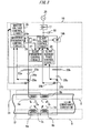
- FIG. 3 is a block diagram of the control device for induction heating units in Embodiment 1 of the present invention.
- a voltage-fed inverter power source 16 includes a rectifier 17, a smoothing capacitor 18, a master inverter 19a, and a slave inverter 19b.
- the rectifier 17 has the function of rectifying an AC power source 20.
- the smoothing capacitor 18 has the function of smoothing a DC voltage output from the rectifier 17.
- the master inverter 19a and the slave inverter 19b are connected in parallel.
- the master inverter 19a and the slave inverter 19b have the function of exerting a PWM control over the DC voltage smoothed by the smoothing capacitor 18.
- a voltage-fed matching device 21 includes a master matching transformer 22a, a master series resonance capacitor 23a, a master current detector 24a, a master voltage detector 25a, a slave matching transformer 22b, a slave series resonance capacitor 23b, a slave current detector 24b, and a slave voltage detector 25b.
- the master matching transformer 22a is connected between the master inverter 19a and the master C-shaped heating unit 5.
- the master series resonance capacitor 23a is connected between the master matching transformer 22a and the master C-shaped heating unit 5.
- the master current detector 24a is connected between the master series resonance capacitor 23a and the master C-shaped heating unit 5.
- the master voltage detector 25a is connected between the master current detector 24a and the master C-shaped heating unit 5.
- the slave matching transformer 22b is connected between the slave inverter 19b and the slave C-shaped heating unit 6.
- the slave series resonance capacitor 23b is connected between the slave matching transformer 22b and the slave C-shaped heating unit 6.
- the slave current detector 24b is connected between the slave series resonance capacitor 23b and the slave C-shaped heating unit 6.
- the slave voltage detector 25b is connected between the slave current detector 24b and the slave C-shaped heating unit 6.
- a master frequency control circuit (a master frequency control part) 26, a slave frequency control circuit (a slave frequency control part) 27, a slave current phase control circuit (a slave current phase control part) 28, a master voltage control circuit (a master voltage control part) 29, and a slave voltage control circuit (a slave voltage control part) 30.
- the master frequency control circuit 26 has the function of setting an operation frequency of the master inverter 19a by receiving the feedback of a detection value of the master current detector 24a and a detection value of the master voltage detector 25a.
- the slave frequency control circuit 27 has the function of setting an operation frequency of the master inverter 19a set by the master frequency control circuit 26 to an operation frequency of the slave inverter 19b.
- the slave current phase control circuit 28 has the function of setting the phase of an output current of the slave inverter 19b by receiving the feedback of a detection value of the master current detector 24a and a detection value of the slave current detector 24b.
- the master voltage control circuit 29 has the function of setting the pulse width of an output voltage from the master inverter 19a by receiving an instruction from the outside and the feedback of a detection value of the master voltage detector 25a.
- the slave voltage control circuit 30 has the function of setting the pulse width of an output voltage from the slave inverter 19b by receiving an instruction from the outside and the feedback of a detection value of the slave voltage detector 25b.
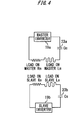
- Figure 4 shows a master-side circuit and a slave-side circuit which are used in the control device for induction heating units in Embodiment 1 of the present invention.
- an electrostatic capacity of the master series resonance capacitor 23a is denoted by Cm
- a load resistance on the master side is denoted by Rm
- a load inductance is denoted by Lm.
- a resonance frequency Fm0 of the master-side circuit is expressed by Equation (1) below.
- the power factor of the master inverter 19a is 1.
- the power factor of the slave inverter 19b is 1.
- control device of this embodiment synchronizes the operation frequency of the master inverter 19a with the operation frequency of the slave inverter 19b.
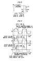
- FIG 5 is an explanatory diagram for the setting procedure for the operation of the master inverter and slave inverter which are used in the control device for induction heating units in Embodiment 1 of the present invention.
- the upper part of Figure 5 shows currents flowing in the master C-shaped heating unit 5 and the slave C-shaped heating unit 6.
- the middle part of Figure 5 shows an output voltage from the master inverter 19a.
- the lower part of Figure shows an output voltage from the slave inverter 19b.
- the master frequency control circuit 26 sets the operation frequency of the master inverter 19a to the resonance frequency Fm0 so that the power factor of the master inverter 19a is equal to 1. That is, as shown in the upper part and middle part of Figure 5 , the operation frequency of the master inverter 19a is set so that the phase of an output voltage Vlm from the master inverter 19a is synchronized with the phase of an output current (a master inductor current lm). As a result, as shown in the upper part and middle part of Figure 5 , the cycle time of the master-side circuit is set to t0.
- the slave frequency control circuit 27 sets the resonance frequency Fm0 of the master-side circuit as the operation frequency of the slave inverter 19b.
- the cycle time of the slave-side circuit is also set to t0.
- the slave current phase control circuit 28 synchronized the phase of an output current (a slave inductor current Is) from the slave inverter 19b with the phase of an output current (a master inductor current Im) from the master inverter 19a.
- a slave inductor current Is an output current from the slave inverter 19b
- a master inductor current Im an output current from the master inverter 19a.
- Figure 6 shows Q-values of the master-side circuit and slave-side circuit of the control device for induction heating units in Embodiment 1 of the present invention.
- a case where the resonance frequency Fm0 of the master-side circuit deviates from the resonance frequency F0s of the slave-side circuit is considered.
- an operation frequency F0 of the master inverter 19a and slave inverter 19b is set to the resonance frequency Fm0 of the master-side circuit.
- a Q-value Qm0 of the master-side circuit is a maximum value on a Q-value curve Qm of the master-side circuit. For this reason, maximum power that can be applied to the master C-shaped heating unit 5 is maintained.
- a Q-value Qs0 of the slave-side circuit is not a maximum value on a Q-value curve Qs of the slave-side circuit. For this reason, maximum power that can be applied to the slave C-shaped heating unit 6 decreases.
- the phase of the output current from the slave inverter 19b is synchronized with the phase of the output current from the master inverter 19a. Pulse widths of output voltages from the master inverter 19a and slave inverter 19b are individually set. For this reason, it is possible to individually control amounts of temperature rise in one side portion and the other side portion of the material to be heated 1 while preventing the occurrence of the abnormal mutual induction phenomenon between the two induction heating units.
- FIG. 7 is a block diagram of a control device for induction heating units in Embodiment 2 of the present invention. Parts which are the same as those in Embodiment 1 or corresponding parts bear identical reference numerals and are not described herein.
- the control device of Embodiment 2 is such that a frequency synchronizing capacitor 31, a disconnecting switch 32, and a slave voltage phase control circuit 33 are added to the control device of Embodiment 1.
- the slave frequency synchronizing capacitor 31 is connected in parallel to the slave series resonance capacitor 23b between the slave matching transformer 22b and the slave C-shaped heating unit 6.
- the disconnecting switch 32 is connected in parallel to the slave series resonance capacitor 23b and connected in series to the slave frequency synchronizing capacitor 31.
- the slave voltage phase control circuit 33 has the function of opening and closing the disconnecting switch 32 by receiving the feedback of the detection value of the slave current detector 24b and the detection value of the slave voltage detector 25b.
- Figure 8 is an explanatory diagram for the resonance frequency of the control device for induction heating units in Embodiment 2 of the present invention.
- an electrostatic capacity of the slave frequency synchronizing capacitor 31 is denoted by Css.
- Figure 9 corresponds to Figure 5 in Embodiment 2 of the present invention.
- the phase of the output current from the master inverter 19a is synchronized with the phase of the output current from the slave inverter 19b.
- the slave voltage phase control circuit 33 synchronizes the phase of the output voltage from the slave inverter 19b with the phase of the output voltage from the master inverter 19a by opening and closing the disconnecting switch 32.
- Figure 10 corresponds to Figure 6 in Embodiment 2 of the present invention.
- the resonance frequency Fm0 of the master-side circuit is synchronized with the resonance frequency Fs0 of the slave-side circuit.
- the Q-value Qm0 of the master-side circuit and the Q-value Qs0 of the slave-side circuit are maximum values. For this reason, maximum power that can be applied to the master C-shaped heating unit 5 and the slave C-shaped heating unit 6 is maintained.
- the phase of the output voltage from the slave inverter 19b is synchronized with the phase of the output voltage from the master inverter 19a by opening and closing the disconnecting switch 32. For this reason, it is possible to prevent a decrease in the heating efficiency of the slave C-shaped heating unit 6.
- FIG 11 is a block diagram of a control device for induction heating units in Embodiment 3 of the present invention. Parts which are the same as those in Embodiment 2 or corresponding parts bear identical reference numerals and are not described herein.
- the control device of Embodiment 3 is such that the disconnecting switch 32 of Embodiment 2 is replaced with a slave voltage phase control device 34.
- the slave voltage phase control circuit 33 controls a voltage applied to the slave frequency synchronizing capacitor 31 through the use of the slave voltage phase control device 34. As a result, the phase of the output voltage from the slave inverter 19b is synchronized with the phase of the output voltage from the master inverter 19a.
- Figure 12 is an explanatory diagram for the resonance frequency of the control device for induction heating units in Embodiment 3 of the present invention.
- the resonance frequency Fs0 of the salve-side circuit changes continuously by controlling the voltage applied to the slave frequency synchronizing capacitor 31.
- Embodiment 3 it is possible to control the voltage applied to the slave frequency synchronizing capacitor 31 through the use of the slave voltage phase control device 34. For this reason, it is possible to ensure synchronizing the phase of the output voltage from the slave inverter 19b with the phase of the output voltage from the master inverter 19a.
- Figure 13 is a block diagram of a control device for induction heating units in Embodiment 4 of the present invention. Parts which are the same as those in Embodiment 2 or corresponding parts bear identical reference numerals and are not described herein.
- the control device of Embodiment 2 uses the slave frequency synchronizing capacitor 31.
- the control device of Embodiment 4 uses a slave frequency synchronizing reactor 35.
- the slave frequency synchronizing reactor 35 is connected in series to the slave series resonance capacitor 23b and connected in parallel to the slave C-shaped heating unit 6.
- the disconnecting switch 32 is connected in series to the slave series resonance capacitor 23b and the slave frequency synchronizing reactor 35 and connected in parallel to the slave C-shaped heating unit 6.
- the slave voltage phase control circuit 33 has the function of synchronizing the phase of the output voltage from the slave inverter 19b with the phase of the output voltage from the master inverter 19a by opening and closing the disconnecting switch 32.
- Figure 14 corresponds to Figure 8 in Embodiment 4 of the present invention.
- inductance of the slave frequency synchronizing reactor 35 is denoted by Lss.
- Embodiment 4 As in Embodiment 2, it is possible to prevent a decrease in the heating efficiency of the slave C-shaped heating unit 6.
- FIG. 15 is a block diagram of a control device for induction heating units in Embodiment 5 of the present invention. Parts which are the same as those in Embodiment 3 or corresponding parts bear identical reference numerals and are not described herein.
- the control device of Embodiment 3 uses the slave frequency synchronizing capacitor 31.
- the control device of Embodiment 4 uses the slave frequency synchronizing reactor 35.
- Figure 16 corresponds to Figure 12 in Embodiment 5 of the present invention.
- the resonance frequency Fs0 of the salve-side circuit changes continuously by controlling the voltage applied to the slave frequency synchronizing reactor 35.
- Embodiment 5 it is possible to control the voltage applied to the slave frequency synchronizing reactor 35 through the use of the slave voltage phase control device 34. For this reason, it is possible to ensure synchronizing the phase of an output voltage of the slave inverter 19b with the phase of the output voltage from the master inverter 19a.
- control device for induction heating units of the present invention can be applied in individually controlling amounts of temperature rise in one side portion and the other side portion of a material to be heated.
Landscapes
- Physics & Mathematics (AREA)
- Electromagnetism (AREA)
- General Induction Heating (AREA)
Description
- The present invention relates to a control device for induction heating units.
- There have been proposed control devices in which a pair of induction heating units arranged in the vicinity of both side portions of a material to be heated is connected in parallel to one power source. According to these control devices, phases of current of the two induction heating units are synchronized. For this reason, an abnormal mutual induction phenomenon does not occur between the two induction heating units (refer to
Patent Literature 1, for example). - Patent Literature 1: Japanese Patent No.
3156746 - However, the same voltage is applied to the two induction heating units described in
Patent Literature 1. For this reason, it is impossible to individually control the power supplied to each of the induction heating units. That is, it is impossible to individually control amounts of temperature rise in one side portion and the other side portion of a material to be heated. - The present invention has been made in order to solve the above-described problem and an object of the present invention is to provide a control device for induction heating units which is capable of individually controlling amounts of temperature rise in one side portion and the other side portion of a material to be heated while preventing the occurrence of an abnormal mutual induction phenomenon between two induction heating units.
- A control device for induction heating units of the present invention includes a master frequency control part that sets an operation frequency of a master inverter, which drives a master C-shaped induction heating unit provided on one side of a material to be heated, so that a phase of an output voltage and a phase of an output current from the master inverter are synchronized;
a slave frequency control part that synchronizes an operation frequency of a slave inverter, which drives a slave C-shaped induction heating unit provided on the other side of the material to be heated, with the operation frequency of the master inverter; a slave current phase control part that synchronizes a phase of an output current from the slave inverter with the phase of the output current from the master inverter; a master voltage control part that sets a pulse width of the output voltage from the master inverter; and a slave voltage control part that sets a pulse width of an output voltage from the slave inverter. - According to the present invention, it is possible to individually control amounts of temperature rise in one side portion and the other side portion of a material to be heated while preventing the occurrence of an abnormal mutual induction phenomenon between two induction heating units.
-
-
Figure 1 is a perspective view of an induction heating unit to which a control device for induction heating units inEmbodiment 1 of the present invention is applied. -
Figure 2 shows induction heating loops of the induction heating unit for which the control device for induction heating units inEmbodiment 1 of the present invention is used. -
Figure 3 is a block diagram of the control device for induction heating units inEmbodiment 1 of the present invention. -
Figure 4 shows a master-side circuit and a slave-side circuit which are used in the control device for induction heating units inEmbodiment 1 of the present invention. -
Figure 5 is an explanatory diagram for the setting procedure for the operation of the master inverter and slave inverter which are used in the control device for induction heating units inEmbodiment 1 of the present invention. -
Figure 6 shows Q-values of the master-side circuit and slave-side circuit of the control device for induction heating units inEmbodiment 1 of the present invention. -
Figure 7 is a block diagram of a control device for induction heating units inEmbodiment 2 of the present invention. -
Figure 8 is an explanatory diagram for the resonance frequency of the control device for induction heating units inEmbodiment 2 of the present invention. -
Figure 9 corresponds toFigure 5 inEmbodiment 2 of the present invention. -
Figure 10 corresponds toFigure 6 inEmbodiment 2 of the present invention. -
Figure 11 is a block diagram of a control device for induction heating units inEmbodiment 3 of the present invention. -
Figure 12 is an explanatory diagram for the resonance frequency of the control device for induction heating units inEmbodiment 3 of the present invention. -
Figure 13 is a block diagram of a control device for induction heating units inEmbodiment 4 of the present invention. -
Figure 14 corresponds toFigure 8 inEmbodiment 4 of the present invention. -
Figure 15 is a block diagram of a control device for induction heating units inEmbodiment 5 of the present invention. -
Figure 16 corresponds toFigure 12 inEmbodiment 5 of the present invention. - Embodiments of the present invention will be described in accordance with the accompanying drawings. In each of the drawings, identical or corresponding parts are referred to by identical and either not described repeatedly or described simply as appropriate.
-
Figure 1 is a perspective view of an induction heating unit to which a control device for induction heating units inEmbodiment 1 of the present invention is applied. - As shown in
Figure 1 , a material to be heated 1 is supported by anentry conveyor roller 2 and adelivery conveyor roller 3. Both end portions of theentry conveyor roller 2 and both end portions of thedelivery conveyor roller 3 are connected togrounds 4. - A master C-
shaped heating unit 5 is arranged in the vicinity of one side of the material to be heated 1. The master C-shaped heating unit 5 includes a master entry C-shaped inductor 5a and a master delivery C-shaped inductor 5b. The master entry C-shaped inductor 5a and the master delivery C-shaped inductor 5b are arranged along the conveyance direction of the material to be heated 1. The master entry C-shaped inductor 5a and the master delivery C-shaped inductor 5b are formed in such a manner that the directions of magnetic flux are reverse to each other. - A slave C-
shaped heating unit 6 is arranged in the vicinity of the other side of the material to be heated 1. The slave C-shaped heating unit 6 includes a slave entry C-shaped inductor 6a and a slave delivery C-shaped inductor 6b. The slave entry C-shaped inductor 6a and the slave delivery C-shaped inductor 6b are arranged along the conveyance direction of the material to be heated 1. The slave entry C-shaped inductor 6a and the slave delivery C-shaped inductor 6b are formed in such a manner that the directions of magnetic flux are reverse to each other. - The master entry C-
shaped inductor 5a and the slave entry C-shaped inductor 6a are formed in such a manner that the directions of magnetic flux are reverse to each other. The master delivery C-shaped inductor 5b and the slave delivery C-shaped inductor 6b are formed in such a manner that the directions of magnetic flux are reverse to each other. - When a current flows in the master entry C-
shaped inductor 5a, an entry inductor magnetic flux is formed. Amaterial current 7a flows in the material to be heated 1 by this entry inductor magnetic flux. When a current flows in the master delivery C-shaped inductor 5b, a delivery inductor magnetic flux is formed. Amaterial current 7b flows in the material to be heated 1 by this delivery inductor magnetic flux. One side portion of the material to be heated 1 is heated by thematerial currents - When a current flows in the slave entry C-
shaped inductor 6a, an entry inductor magnetic flux is formed. Amaterial current 7c flows in the material to be heated 1 by this entry inductor magnetic flux. When a current flows in the slave delivery C-shaped inductor 6b, a delivery inductor magnetic flux is formed. Amaterial current 7d flows in the material to be heated 1 by this delivery inductor magnetic flux. The other side portion of the material to be heated 1 is heated by thematerial currents - On this occasion, between one end of the
entry conveyor roller 2 and a portion in the vicinity of the master entry C-shaped inductor 5a, aground current 8a can flow in the material to be heated 1. Between one end of thedelivery conveyor roller 3 and a portion in the vicinity of the master delivery C-shaped inductor 5b, aground current 8b can flow in the material to be heated 1. Between the other end of theentry conveyor roller 2 and a portion in the vicinity of the slave entry C-shaped inductor 6a, aground current 8c can flow in the material to be heated 1. Between the other end of thedelivery conveyor roller 3 and a portion in the vicinity of the slave delivery C-shapedinductor 6b, a ground current 8d can flow in the material to be heated 1. - In a case where the ground current 8a is high, an
arc 9 can be formed at a contact point between one end of theentry conveyor roller 2 and the material to be heated 1. In a case where the ground current 8b is high, anarc 9 can be formed at a contact point between one end of thedelivery conveyor roller 3 and the material to be heated 1. In a case where the ground current 8c is high, anarc 9 can be formed at a contact point between the other end of theentry conveyor roller 2 and the material to be heated 1. In a case where the ground current 8d is high, anarc 9 can be formed at a contact point between the other end of thedelivery conveyor roller 3 and the material to be heated 1. - Next, a method of preventing the formation of the
arc 9 will be described with the aid ofFigure 2 . -
Figure 2 shows induction heating loops of the induction heating unit for which the control device for induction heating units inEmbodiment 1 of the present invention is used. - A first
material loop circuit 10, a secondmaterial loop circuit 11, and aground loop circuit 12 are formed on the master side and the slave side. - The first
material loop circuit 10 includes an entry material resistor R1 and an entry material end resistor R2 of the material to be heated 1. The secondmaterial loop circuit 11 includes a delivery material resistor R3 and a delivery material end resistor R4 of the material to be heated 1. Theground loop circuit 12 includes a ground resistor R0, the entry material end resistor R2, and the delivery material end resistor R4. - An entry inductor magnetic flux φ1 penetrates through the first
material loop circuit 10. An entry material current 13 flows by this penetration. In contrast to this, a delivery inductor magnetic flux φ2 penetrates through the secondmaterial loop circuit 11. A delivery material current 14 flows by this penetration. - In contrast to this, in the
ground loop circuit 12, the amount of the entry inductor magnetic flux φ1 and the amount of the delivery inductor magnetic flux φ2 are identical in the directions reverse to each other. For this reason, the composite magnetic flux of the entry inductor magnetic flux φ1 and the delivery inductor magnetic flux φ2 is zero. As a result, a ground current 15 flowing between theentry conveyor roller 2 and theground 4, the ground current 15 flowing in the material to be heated 1, and the ground current 15 flowing between thedelivery conveyor roller 3 and theground 4 are zero. For this reason, thearc 9 is not formed. That is, arc damage does not occur on the surface of theentry conveyor roller 2, the surface of thedelivery conveyor roller 3, and the surface of the material to be heated 1, either. - Next, the control device for induction heating units will be described with the aid of
Figure 3 . -
Figure 3 is a block diagram of the control device for induction heating units inEmbodiment 1 of the present invention. - In
Figure 3 , a voltage-fedinverter power source 16 includes arectifier 17, a smoothingcapacitor 18, amaster inverter 19a, and aslave inverter 19b. - The
rectifier 17 has the function of rectifying anAC power source 20. The smoothingcapacitor 18 has the function of smoothing a DC voltage output from therectifier 17. Themaster inverter 19a and theslave inverter 19b are connected in parallel. Themaster inverter 19a and theslave inverter 19b have the function of exerting a PWM control over the DC voltage smoothed by the smoothingcapacitor 18. - A voltage-fed
matching device 21 includes amaster matching transformer 22a, a masterseries resonance capacitor 23a, a mastercurrent detector 24a, amaster voltage detector 25a, aslave matching transformer 22b, a slaveseries resonance capacitor 23b, a slavecurrent detector 24b, and aslave voltage detector 25b. - The
master matching transformer 22a is connected between themaster inverter 19a and the master C-shapedheating unit 5. The masterseries resonance capacitor 23a is connected between themaster matching transformer 22a and the master C-shapedheating unit 5. The mastercurrent detector 24a is connected between the masterseries resonance capacitor 23a and the master C-shapedheating unit 5. Themaster voltage detector 25a is connected between the mastercurrent detector 24a and the master C-shapedheating unit 5. - The
slave matching transformer 22b is connected between theslave inverter 19b and the slave C-shapedheating unit 6. The slaveseries resonance capacitor 23b is connected between theslave matching transformer 22b and the slave C-shapedheating unit 6. The slavecurrent detector 24b is connected between the slaveseries resonance capacitor 23b and the slave C-shapedheating unit 6. Theslave voltage detector 25b is connected between the slavecurrent detector 24b and the slave C-shapedheating unit 6. - In this embodiment, there are provided a master frequency control circuit (a master frequency control part) 26, a slave frequency control circuit (a slave frequency control part) 27, a slave current phase control circuit (a slave current phase control part) 28, a master voltage control circuit (a master voltage control part) 29, and a slave voltage control circuit (a slave voltage control part) 30.
- The master
frequency control circuit 26 has the function of setting an operation frequency of themaster inverter 19a by receiving the feedback of a detection value of the mastercurrent detector 24a and a detection value of themaster voltage detector 25a. The slavefrequency control circuit 27 has the function of setting an operation frequency of themaster inverter 19a set by the masterfrequency control circuit 26 to an operation frequency of theslave inverter 19b. The slave currentphase control circuit 28 has the function of setting the phase of an output current of theslave inverter 19b by receiving the feedback of a detection value of the mastercurrent detector 24a and a detection value of the slavecurrent detector 24b. - The master
voltage control circuit 29 has the function of setting the pulse width of an output voltage from themaster inverter 19a by receiving an instruction from the outside and the feedback of a detection value of themaster voltage detector 25a. The slavevoltage control circuit 30 has the function of setting the pulse width of an output voltage from theslave inverter 19b by receiving an instruction from the outside and the feedback of a detection value of theslave voltage detector 25b. - Next, operation frequencies of the
master inverter 19a and theslave inverter 19b will be described with the aid ofFigure 4 . -
Figure 4 shows a master-side circuit and a slave-side circuit which are used in the control device for induction heating units inEmbodiment 1 of the present invention. - As shown in
Figure 4 , an electrostatic capacity of the masterseries resonance capacitor 23a is denoted by Cm, a load resistance on the master side is denoted by Rm, and a load inductance is denoted by Lm. In this case, a resonance frequency Fm0 of the master-side circuit is expressed by Equation (1) below. - [Equation 1]

- As shown in
Figure 4 , an electrostatic capacity of the slaveseries resonance capacitor 23b is denoted by Cs, a load resistance on the slave side is denoted by Rs, and a load inductance is denoted by Ls. In this case, a resonance frequency Fs0 of the slave-side circuit is expressed by Equation (2) below.
[Equation 2]
- If the
master inverter 19a operates with the resonance frequency Fm0, the power factor of themaster inverter 19a is 1. In contrast to this, if theslave inverter 19b operates with the resonance frequency Fs0, the power factor of theslave inverter 19b is 1. - However, usually, Fm0 and Fs0 are different. For this reason, if the
master inverter 19a operates with the resonance frequency Fm0 and theslave inverter 19b operates with the resonance frequency Fs0, then an abnormal mutual inductance phenomenon occurs between the master C-shapedheating unit 5 and the slave C-shapedheating unit 6. - Therefore, the control device of this embodiment synchronizes the operation frequency of the
master inverter 19a with the operation frequency of theslave inverter 19b. - Next, a setting procedure for the operation of the
master inverter 19a and theslave inverter 19b will be described with the aid ofFigure 5 . -
Figure 5 is an explanatory diagram for the setting procedure for the operation of the master inverter and slave inverter which are used in the control device for induction heating units inEmbodiment 1 of the present invention. - The upper part of
Figure 5 shows currents flowing in the master C-shapedheating unit 5 and the slave C-shapedheating unit 6. The middle part ofFigure 5 shows an output voltage from themaster inverter 19a. The lower part of Figure shows an output voltage from theslave inverter 19b. - First, the master
frequency control circuit 26 sets the operation frequency of themaster inverter 19a to the resonance frequency Fm0 so that the power factor of themaster inverter 19a is equal to 1. That is, as shown in the upper part and middle part ofFigure 5 , the operation frequency of themaster inverter 19a is set so that the phase of an output voltage Vlm from themaster inverter 19a is synchronized with the phase of an output current (a master inductor current lm). As a result, as shown in the upper part and middle part ofFigure 5 , the cycle time of the master-side circuit is set to t0. - Thereafter, the slave
frequency control circuit 27 sets the resonance frequency Fm0 of the master-side circuit as the operation frequency of theslave inverter 19b. As a result, as shown in the lower part ofFigure 5 , the cycle time of the slave-side circuit is also set to t0. - Thereafter, as shown in the upper part of
Figure 5 , the slave currentphase control circuit 28 synchronized the phase of an output current (a slave inductor current Is) from theslave inverter 19b with the phase of an output current (a master inductor current Im) from themaster inverter 19a. As a result, in the master C-shapedheating unit 5 and the slave C-shapedheating unit 6, the generation of a beat current by a mutual induction current is suppressed. That is, the master C-shapedheating unit 5 and the slave C-shapedheating unit 6 can avoid failures by the flow of an overcurrent. - Next, Q-values of the master-side circuit and slave-side circuit will be described with the aid of
Figure 6 . -
Figure 6 shows Q-values of the master-side circuit and slave-side circuit of the control device for induction heating units inEmbodiment 1 of the present invention. - As shown in
Figure 6 , a case where the resonance frequency Fm0 of the master-side circuit deviates from the resonance frequency F0s of the slave-side circuit is considered. In this case, an operation frequency F0 of themaster inverter 19a andslave inverter 19b is set to the resonance frequency Fm0 of the master-side circuit. In this case, a Q-value Qm0 of the master-side circuit is a maximum value on a Q-value curve Qm of the master-side circuit. For this reason, maximum power that can be applied to the master C-shapedheating unit 5 is maintained. In contrast to this, a Q-value Qs0 of the slave-side circuit is not a maximum value on a Q-value curve Qs of the slave-side circuit. For this reason, maximum power that can be applied to the slave C-shapedheating unit 6 decreases. - According to
Embodiment 1 described above, the phase of the output current from theslave inverter 19b is synchronized with the phase of the output current from themaster inverter 19a. Pulse widths of output voltages from themaster inverter 19a andslave inverter 19b are individually set. For this reason, it is possible to individually control amounts of temperature rise in one side portion and the other side portion of the material to be heated 1 while preventing the occurrence of the abnormal mutual induction phenomenon between the two induction heating units. -
Figure 7 is a block diagram of a control device for induction heating units inEmbodiment 2 of the present invention. Parts which are the same as those inEmbodiment 1 or corresponding parts bear identical reference numerals and are not described herein. - The control device of
Embodiment 2 is such that afrequency synchronizing capacitor 31, a disconnectingswitch 32, and a slave voltagephase control circuit 33 are added to the control device ofEmbodiment 1. - The slave
frequency synchronizing capacitor 31 is connected in parallel to the slaveseries resonance capacitor 23b between theslave matching transformer 22b and the slave C-shapedheating unit 6. The disconnectingswitch 32 is connected in parallel to the slaveseries resonance capacitor 23b and connected in series to the slavefrequency synchronizing capacitor 31. The slave voltagephase control circuit 33 has the function of opening and closing the disconnectingswitch 32 by receiving the feedback of the detection value of the slavecurrent detector 24b and the detection value of theslave voltage detector 25b. - Next, the resonance frequency of the slave-side circuit will be described with the aid of
Figure 8 . -
Figure 8 is an explanatory diagram for the resonance frequency of the control device for induction heating units inEmbodiment 2 of the present invention. - As shown in
Figure 8 , an electrostatic capacity of the slavefrequency synchronizing capacitor 31 is denoted by Css. In a case where the disconnectingswitch 32 is closed, the resonance frequency Fs0 of the slave-side circuit is expressed by Equation (3) below.
[Equation 3]
- Next, a setting procedure for operation frequencies of the
master inverter 19a and the slave inverter will be described with the aid ofFigure 9 . -
Figure 9 corresponds toFigure 5 inEmbodiment 2 of the present invention. - Similarly to
Figure 5 , inFigure 9 the phase of the output current from themaster inverter 19a is synchronized with the phase of the output current from theslave inverter 19b. Thereafter, the slave voltagephase control circuit 33 synchronizes the phase of the output voltage from theslave inverter 19b with the phase of the output voltage from themaster inverter 19a by opening and closing the disconnectingswitch 32. - Next, Q-values of the master-side circuit and slave-side circuit will be described with the aid of
Figure 10 . -
Figure 10 corresponds toFigure 6 inEmbodiment 2 of the present invention. - As shown in
Figure 10 , the resonance frequency Fm0 of the master-side circuit is synchronized with the resonance frequency Fs0 of the slave-side circuit. In this case, the Q-value Qm0 of the master-side circuit and the Q-value Qs0 of the slave-side circuit are maximum values. For this reason, maximum power that can be applied to the master C-shapedheating unit 5 and the slave C-shapedheating unit 6 is maintained. - According to
Embodiment 2 described above, the phase of the output voltage from theslave inverter 19b is synchronized with the phase of the output voltage from themaster inverter 19a by opening and closing the disconnectingswitch 32. For this reason, it is possible to prevent a decrease in the heating efficiency of the slave C-shapedheating unit 6. -
Figure 11 is a block diagram of a control device for induction heating units inEmbodiment 3 of the present invention. Parts which are the same as those inEmbodiment 2 or corresponding parts bear identical reference numerals and are not described herein. - The control device of
Embodiment 3 is such that the disconnectingswitch 32 ofEmbodiment 2 is replaced with a slave voltagephase control device 34. - The slave voltage
phase control circuit 33 controls a voltage applied to the slavefrequency synchronizing capacitor 31 through the use of the slave voltagephase control device 34. As a result, the phase of the output voltage from theslave inverter 19b is synchronized with the phase of the output voltage from themaster inverter 19a. - Next, the resonance frequency of the slave-side circuit will be described with the aid of
Figure 12 . -
Figure 12 is an explanatory diagram for the resonance frequency of the control device for induction heating units inEmbodiment 3 of the present invention. - In
Figure 12 , the resonance frequency Fs0 of the salve-side circuit changes continuously by controlling the voltage applied to the slavefrequency synchronizing capacitor 31. - According to
Embodiment 3 described above, it is possible to control the voltage applied to the slavefrequency synchronizing capacitor 31 through the use of the slave voltagephase control device 34. For this reason, it is possible to ensure synchronizing the phase of the output voltage from theslave inverter 19b with the phase of the output voltage from themaster inverter 19a. -
Figure 13 is a block diagram of a control device for induction heating units inEmbodiment 4 of the present invention. Parts which are the same as those inEmbodiment 2 or corresponding parts bear identical reference numerals and are not described herein. - The control device of
Embodiment 2 uses the slavefrequency synchronizing capacitor 31. On the other hand, the control device ofEmbodiment 4 uses a slavefrequency synchronizing reactor 35. - The slave
frequency synchronizing reactor 35 is connected in series to the slaveseries resonance capacitor 23b and connected in parallel to the slave C-shapedheating unit 6. The disconnectingswitch 32 is connected in series to the slaveseries resonance capacitor 23b and the slavefrequency synchronizing reactor 35 and connected in parallel to the slave C-shapedheating unit 6. The slave voltagephase control circuit 33 has the function of synchronizing the phase of the output voltage from theslave inverter 19b with the phase of the output voltage from themaster inverter 19a by opening and closing the disconnectingswitch 32. - Next, the resonance frequency of the slave-side circuit will be described with the aid of
Figure 14 . -
Figure 14 corresponds toFigure 8 inEmbodiment 4 of the present invention. - As shown in
Figure 14 , inductance of the slavefrequency synchronizing reactor 35 is denoted by Lss. In a case where the disconnectingswitch 32 is closed, the resonance frequency Fs0 of the slave-side circuit is expressed by Equation (4) below.
[Equation 4]
- According to
Embodiment 4 described above, as inEmbodiment 2, it is possible to prevent a decrease in the heating efficiency of the slave C-shapedheating unit 6. -
Figure 15 is a block diagram of a control device for induction heating units inEmbodiment 5 of the present invention. Parts which are the same as those inEmbodiment 3 or corresponding parts bear identical reference numerals and are not described herein. - The control device of
Embodiment 3 uses the slavefrequency synchronizing capacitor 31. On the other hand, the control device ofEmbodiment 4 uses the slavefrequency synchronizing reactor 35. - Next, the resonance frequency of the slave-side circuit will be described with the aid of
Figure 16 . -
Figure 16 corresponds toFigure 12 inEmbodiment 5 of the present invention. - In
Figure 16 , the resonance frequency Fs0 of the salve-side circuit changes continuously by controlling the voltage applied to the slavefrequency synchronizing reactor 35. - According to
Embodiment 5 described above, it is possible to control the voltage applied to the slavefrequency synchronizing reactor 35 through the use of the slave voltagephase control device 34. For this reason, it is possible to ensure synchronizing the phase of an output voltage of theslave inverter 19b with the phase of the output voltage from themaster inverter 19a. - As described so far, the control device for induction heating units of the present invention can be applied in individually controlling amounts of temperature rise in one side portion and the other side portion of a material to be heated.
- 1 material to be heated, 2 entry conveyor roller, 3 delivery conveyor roller, 4 ground, 5 master C-shaped heating unit, 5a master entry C-shaped inductor, 5b master delivery C-shaped inductor, 6 slave C-shaped heating unit, 6a slave entry C-shaped inductor, 6b slave delivery C-shaped inductor, 7a-7d material current, 8a-8d ground current, 9 arc, 10 first material loop circuit, 11 second material loop circuit, 12 ground loop circuit, 13,14 material current, 15 ground current, 16 voltage-fed inverter power source, 17 rectifier, 18 smoothing capacitor, 19a master inverter, 19b slave inverter, 20 AC power source, 21 voltage-fed matching device, 22a master matching transformer, 22b slave matching transformer, 23a master series resonance capacitor, 23b slave series resonance capacitor, 24a master current detector, 24b slave current detector, 25a master voltage detector, 25b slave voltage detector, 26 master frequency control circuit, 27 slave frequency control circuit, 28 slave current phase control circuit, 29 master voltage control circuit, 30 slave voltage control circuit, 31 frequency synchronizing capacitor, 32 disconnecting switch, 33 slave voltage phase control circuit, 34 slave voltage phase control device, 35 slave frequency synchronizing reactor
Claims (6)
- A control device for induction heating units, comprising:a master frequency control part that sets an operation frequency of a master inverter, which drives a master C-shaped induction heating unit provided on one side of a material to be heated, so that a phase of an output voltage and a phase of an output current from the master inverter are synchronized;a slave frequency control part that synchronizes an operation frequency of a slave inverter, which drives a slave C-shaped induction heating unit provided on the other side of the material to be heated, with the operation frequency of the master inverter;a slave current phase control part that synchronizes a phase of an output current from the slave inverter with the phase of the output current from the master inverter;a master voltage control part that sets a pulse width of the output voltage from the master inverter; anda slave voltage control part that sets a pulse width of an output voltage from the slave inverter.
- The control device for induction heating units according to claim 1, further comprising:a slave voltage phase control part that synchronizes a phase of the output voltage from the slave inverter with the phase of the output voltage from the master inverter.
- The control device for induction heating units according to claim 2, further comprising:a slave series resonance capacitor connected between the slave C-shaped heating unit and the slave inverter;a slave frequency synchronizing capacitor connected in parallel to the slave series resonance capacitor; anda disconnecting switch connected in parallel to the slave series resonance capacitor and connected in series to the slave frequency synchronizing capacitor,wherein the slave voltage phase control part synchronizes the phase of the output voltage from the slave inverter with the phase of the output voltage from the master inverter by opening and closing the disconnecting switch.
- The control device for induction heating units according to claim 2, further comprising:a slave series resonance capacitor connected between the slave C-shaped heating unit and the slave inverter;a slave frequency synchronizing capacitor connected in parallel to the slave series resonance capacitor; anda slave voltage phase control device connected in parallel to the slave series resonance capacitor and connected in series to the slave frequency synchronizing capacitor,wherein the slave voltage phase control part synchronizes the phase of the output voltage from the slave inverter with the phase of the output voltage from the master inverter by controlling a voltage applied to the slave frequency synchronizing capacitor through the use of the slave voltage phase control device.
- The control device for induction heating units according to claim 2, further comprising:a slave series resonance capacitor connected between the slave C-shaped heating unit and the slave inverter;a slave frequency synchronizing reactor connected in series to the slave series resonance capacitor and connected in parallel to the slave C-shaped heating unit; anda disconnecting switch connected in series to the slave series resonance capacitor and the slave frequency synchronizing reactor and connected in parallel to the slave C-shaped heating unit,wherein the slave voltage phase control part synchronizes the phase of the output voltage from the slave inverter with the phase of the output voltage from the master inverter by opening and closing the disconnecting switch.
- The control device for induction heating units according to claim 2, further comprising:a slave series resonance capacitor connected between the slave C-shaped heating unit and the slave inverter;a slave frequency synchronizing reactor connected in series to the slave series resonance capacitor and connected in parallel to the slave C-shaped heating unit; anda slave voltage phase control device connected in series to the slave series resonance capacitor and the slave frequency synchronizing reactor and connected in parallel to the slave C-shaped heating unit,wherein the slave voltage phase control part synchronizes the phase of the output voltage from the slave inverter with the phase of the output voltage from the master inverter by controlling a voltage applied to the slave frequency synchronizing reactor through use of the slave voltage phase control device.
Applications Claiming Priority (1)
| Application Number | Priority Date | Filing Date | Title |
|---|---|---|---|
| PCT/JP2012/071565 WO2014033805A1 (en) | 2012-08-27 | 2012-08-27 | Control device for induction heating units |
Publications (3)
| Publication Number | Publication Date |
|---|---|
| EP2890217A1 true EP2890217A1 (en) | 2015-07-01 |
| EP2890217A4 EP2890217A4 (en) | 2016-06-15 |
| EP2890217B1 EP2890217B1 (en) | 2020-01-08 |
Family
ID=50182656
Family Applications (1)
| Application Number | Title | Priority Date | Filing Date |
|---|---|---|---|
| EP12883809.1A Active EP2890217B1 (en) | 2012-08-27 | 2012-08-27 | Control device for induction heating units |
Country Status (8)
| Country | Link |
|---|---|
| EP (1) | EP2890217B1 (en) |
| JP (1) | JP5983748B2 (en) |
| KR (1) | KR101617132B1 (en) |
| CN (1) | CN104584683B (en) |
| BR (1) | BR112015004000B1 (en) |
| IN (1) | IN2015DN00902A (en) |
| TW (1) | TWI565365B (en) |
| WO (1) | WO2014033805A1 (en) |
Cited By (1)
| Publication number | Priority date | Publication date | Assignee | Title |
|---|---|---|---|---|
| EP3790180A1 (en) * | 2019-09-04 | 2021-03-10 | IAS GmbH | Device and method for inductive heating of metal material |
Families Citing this family (2)
| Publication number | Priority date | Publication date | Assignee | Title |
|---|---|---|---|---|
| JP6391175B2 (en) * | 2015-10-06 | 2018-09-19 | 東芝三菱電機産業システム株式会社 | Induction heating device |
| KR102744519B1 (en) * | 2022-05-19 | 2024-12-20 | 파이온일렉트릭 주식회사 | Gridforming type inertial output auxiliary control device |
Family Cites Families (15)
| Publication number | Priority date | Publication date | Assignee | Title |
|---|---|---|---|---|
| JPS593498U (en) * | 1982-06-29 | 1984-01-10 | 富士電機株式会社 | Power factor adjustment device for high frequency induction furnace |
| JPH03156746A (en) | 1989-11-14 | 1991-07-04 | Hitachi Maxell Ltd | Production of optical information recording medium |
| JPH05192775A (en) * | 1991-01-18 | 1993-08-03 | Mitsubishi Electric Corp | Plate pressure welding method |
| JP2581374B2 (en) * | 1992-04-22 | 1997-02-12 | 住友金属工業株式会社 | Induction heating device |
| JP3112560B2 (en) * | 1992-05-08 | 2000-11-27 | 日本金属株式会社 | High frequency welding equipment |
| JP3156746B2 (en) * | 1994-06-21 | 2001-04-16 | 北芝電機株式会社 | Induction heating device |
| JP2002260833A (en) * | 2000-12-27 | 2002-09-13 | Mitsui Eng & Shipbuild Co Ltd | Induction heating method and apparatus |
| JP2002313547A (en) * | 2001-04-09 | 2002-10-25 | Mitsui Eng & Shipbuild Co Ltd | Induction heating equipment for plate materials |
| EP2405711B1 (en) * | 2002-06-26 | 2015-05-06 | Mitsui Engineering and Shipbuilding Co, Ltd. | Induction heating method and unit |
| KR100750546B1 (en) * | 2002-06-26 | 2007-08-20 | 미쯔이 죠센 가부시키가이샤 | Induction heating method and apparatus |
| TW564658B (en) * | 2002-06-27 | 2003-12-01 | Mitsui Shipbuilding Eng | Inductive heating method and device |
| JP5388109B2 (en) * | 2009-04-10 | 2014-01-15 | 三井造船株式会社 | Induction heating apparatus, control method thereof, and program |
| JP5053332B2 (en) * | 2009-06-30 | 2012-10-17 | 島田理化工業株式会社 | Induction heating device |
| JP5466905B2 (en) * | 2009-09-16 | 2014-04-09 | 東芝三菱電機産業システム株式会社 | Induction heating apparatus and control method of induction heating apparatus |
| JP5063755B2 (en) * | 2010-08-09 | 2012-10-31 | 三井造船株式会社 | Induction heating apparatus and induction heating method |
-
2012
- 2012-08-27 KR KR1020157005554A patent/KR101617132B1/en active Active
- 2012-08-27 EP EP12883809.1A patent/EP2890217B1/en active Active
- 2012-08-27 BR BR112015004000-4A patent/BR112015004000B1/en active IP Right Grant
- 2012-08-27 CN CN201280075524.6A patent/CN104584683B/en active Active
- 2012-08-27 JP JP2014532589A patent/JP5983748B2/en active Active
- 2012-08-27 WO PCT/JP2012/071565 patent/WO2014033805A1/en not_active Ceased
- 2012-12-14 TW TW101147389A patent/TWI565365B/en active
-
2015
- 2015-02-04 IN IN902DEN2015 patent/IN2015DN00902A/en unknown
Cited By (1)
| Publication number | Priority date | Publication date | Assignee | Title |
|---|---|---|---|---|
| EP3790180A1 (en) * | 2019-09-04 | 2021-03-10 | IAS GmbH | Device and method for inductive heating of metal material |
Also Published As
| Publication number | Publication date |
|---|---|
| BR112015004000A2 (en) | 2017-07-04 |
| KR101617132B1 (en) | 2016-04-29 |
| WO2014033805A1 (en) | 2014-03-06 |
| EP2890217B1 (en) | 2020-01-08 |
| KR20150041020A (en) | 2015-04-15 |
| JPWO2014033805A1 (en) | 2016-08-08 |
| JP5983748B2 (en) | 2016-09-06 |
| IN2015DN00902A (en) | 2015-06-12 |
| TWI565365B (en) | 2017-01-01 |
| CN104584683B (en) | 2016-08-17 |
| BR112015004000B1 (en) | 2020-11-10 |
| TW201410077A (en) | 2014-03-01 |
| EP2890217A4 (en) | 2016-06-15 |
| CN104584683A (en) | 2015-04-29 |
Similar Documents
| Publication | Publication Date | Title |
|---|---|---|
| JP6991867B2 (en) | Load control for bidirectional induction power transfer systems | |
| EP2800454B1 (en) | Induction heating cooker | |
| Tsang et al. | Rapid islanding detection using multi-level inverter for grid-interactive PV system | |
| EP2890217B1 (en) | Control device for induction heating units | |
| JP2014113007A (en) | Electric power conversion system, reactor loss calculation method, and reactor protection method | |
| JP4406585B2 (en) | Induction voltage detection method and apparatus, and induction heating system | |
| Chung et al. | System conditions monitoring method for a wireless cellular phone charger | |
| EP3065504B1 (en) | Induction heating system | |
| EP2476178B1 (en) | Adaptive control method and adaptive controller for controlling energy supplied to a resonant tank | |
| KR101388398B1 (en) | State estimator based voltage control method and apparatus of an inverter with output lc filter for application to uninterruptable power supply | |
| JP5776287B2 (en) | Induction heating power supply | |
| JP4596960B2 (en) | Electromagnetic induction heating device, electromagnetic induction heating cooking device | |
| JP6486983B2 (en) | Abnormality detection apparatus and abnormality detection method for induction melting furnace | |
| JPH033670A (en) | Method of controlling induction heating inverter | |
| ITMI20010910A1 (en) | INDUCTION COOKING EQUIPMENT HAVING IMPROVED FEATURES | |
| JP6854428B2 (en) | Inverter device and its control method | |
| Costa et al. | Hybrid high-power rectifier with reduced THDI and voltage sag ride-through capability | |
| EP3465870B1 (en) | A method, a controller and a network | |
| JP2007157494A (en) | Induction heating device | |
| RU2520572C1 (en) | Power supply source for electric installations | |
| JP2013251275A (en) | Induction heating apparatus | |
| JP2002093563A (en) | Control method of electromagnetic cooker power supply | |
| KR20120122978A (en) | Resonant circuit inverter with a controllable working point | |
| JP2012160478A (en) | Induction heating apparatus | |
| ITTO980132A1 (en) | HIGH FREQUENCY GENERATOR FOR THE INDUCTION WELDING OF PACKAGING IN CONTAINING VERSABLE FOOD PRODUCTS. |
Legal Events
| Date | Code | Title | Description |
|---|---|---|---|
| PUAI | Public reference made under article 153(3) epc to a published international application that has entered the european phase |
Free format text: ORIGINAL CODE: 0009012 |
|
| 17P | Request for examination filed |
Effective date: 20150220 |
|
| AK | Designated contracting states |
Kind code of ref document: A1 Designated state(s): AL AT BE BG CH CY CZ DE DK EE ES FI FR GB GR HR HU IE IS IT LI LT LU LV MC MK MT NL NO PL PT RO RS SE SI SK SM TR |
|
| AX | Request for extension of the european patent |
Extension state: BA ME |
|
| DAX | Request for extension of the european patent (deleted) | ||
| RA4 | Supplementary search report drawn up and despatched (corrected) |
Effective date: 20160518 |
|
| RIC1 | Information provided on ipc code assigned before grant |
Ipc: H05B 6/06 20060101AFI20160511BHEP Ipc: H05B 6/10 20060101ALI20160511BHEP Ipc: H05B 6/14 20060101ALI20160511BHEP |
|
| STAA | Information on the status of an ep patent application or granted ep patent |
Free format text: STATUS: EXAMINATION IS IN PROGRESS |
|
| 17Q | First examination report despatched |
Effective date: 20170303 |
|
| GRAP | Despatch of communication of intention to grant a patent |
Free format text: ORIGINAL CODE: EPIDOSNIGR1 |
|
| STAA | Information on the status of an ep patent application or granted ep patent |
Free format text: STATUS: GRANT OF PATENT IS INTENDED |
|
| INTG | Intention to grant announced |
Effective date: 20190912 |
|
| RAP1 | Party data changed (applicant data changed or rights of an application transferred) |
Owner name: TOSHIBA MITSUBISHI-ELECTRIC INDUSTRIAL SYSTEMS COR |
|
| RIN1 | Information on inventor provided before grant (corrected) |
Inventor name: DOIZAKI, TETSUJI |
|
| GRAS | Grant fee paid |
Free format text: ORIGINAL CODE: EPIDOSNIGR3 |
|
| GRAA | (expected) grant |
Free format text: ORIGINAL CODE: 0009210 |
|
| STAA | Information on the status of an ep patent application or granted ep patent |
Free format text: STATUS: THE PATENT HAS BEEN GRANTED |
|
| AK | Designated contracting states |
Kind code of ref document: B1 Designated state(s): AL AT BE BG CH CY CZ DE DK EE ES FI FR GB GR HR HU IE IS IT LI LT LU LV MC MK MT NL NO PL PT RO RS SE SI SK SM TR |
|
| REG | Reference to a national code |
Ref country code: GB Ref legal event code: FG4D |
|
| REG | Reference to a national code |
Ref country code: CH Ref legal event code: EP |
|
| REG | Reference to a national code |
Ref country code: DE Ref legal event code: R096 Ref document number: 602012067193 Country of ref document: DE |
|
| REG | Reference to a national code |
Ref country code: IE Ref legal event code: FG4D |
|
| REG | Reference to a national code |
Ref country code: AT Ref legal event code: REF Ref document number: 1224326 Country of ref document: AT Kind code of ref document: T Effective date: 20200215 |
|
| REG | Reference to a national code |
Ref country code: NL Ref legal event code: MP Effective date: 20200108 |
|
| REG | Reference to a national code |
Ref country code: LT Ref legal event code: MG4D |
|
| PG25 | Lapsed in a contracting state [announced via postgrant information from national office to epo] |
Ref country code: NO Free format text: LAPSE BECAUSE OF FAILURE TO SUBMIT A TRANSLATION OF THE DESCRIPTION OR TO PAY THE FEE WITHIN THE PRESCRIBED TIME-LIMIT Effective date: 20200408 Ref country code: FI Free format text: LAPSE BECAUSE OF FAILURE TO SUBMIT A TRANSLATION OF THE DESCRIPTION OR TO PAY THE FEE WITHIN THE PRESCRIBED TIME-LIMIT Effective date: 20200108 Ref country code: LT Free format text: LAPSE BECAUSE OF FAILURE TO SUBMIT A TRANSLATION OF THE DESCRIPTION OR TO PAY THE FEE WITHIN THE PRESCRIBED TIME-LIMIT Effective date: 20200108 Ref country code: NL Free format text: LAPSE BECAUSE OF FAILURE TO SUBMIT A TRANSLATION OF THE DESCRIPTION OR TO PAY THE FEE WITHIN THE PRESCRIBED TIME-LIMIT Effective date: 20200108 Ref country code: PT Free format text: LAPSE BECAUSE OF FAILURE TO SUBMIT A TRANSLATION OF THE DESCRIPTION OR TO PAY THE FEE WITHIN THE PRESCRIBED TIME-LIMIT Effective date: 20200531 Ref country code: RS Free format text: LAPSE BECAUSE OF FAILURE TO SUBMIT A TRANSLATION OF THE DESCRIPTION OR TO PAY THE FEE WITHIN THE PRESCRIBED TIME-LIMIT Effective date: 20200108 |
|
| PG25 | Lapsed in a contracting state [announced via postgrant information from national office to epo] |
Ref country code: HR Free format text: LAPSE BECAUSE OF FAILURE TO SUBMIT A TRANSLATION OF THE DESCRIPTION OR TO PAY THE FEE WITHIN THE PRESCRIBED TIME-LIMIT Effective date: 20200108 Ref country code: BG Free format text: LAPSE BECAUSE OF FAILURE TO SUBMIT A TRANSLATION OF THE DESCRIPTION OR TO PAY THE FEE WITHIN THE PRESCRIBED TIME-LIMIT Effective date: 20200408 Ref country code: GR Free format text: LAPSE BECAUSE OF FAILURE TO SUBMIT A TRANSLATION OF THE DESCRIPTION OR TO PAY THE FEE WITHIN THE PRESCRIBED TIME-LIMIT Effective date: 20200409 Ref country code: SE Free format text: LAPSE BECAUSE OF FAILURE TO SUBMIT A TRANSLATION OF THE DESCRIPTION OR TO PAY THE FEE WITHIN THE PRESCRIBED TIME-LIMIT Effective date: 20200108 Ref country code: LV Free format text: LAPSE BECAUSE OF FAILURE TO SUBMIT A TRANSLATION OF THE DESCRIPTION OR TO PAY THE FEE WITHIN THE PRESCRIBED TIME-LIMIT Effective date: 20200108 Ref country code: IS Free format text: LAPSE BECAUSE OF FAILURE TO SUBMIT A TRANSLATION OF THE DESCRIPTION OR TO PAY THE FEE WITHIN THE PRESCRIBED TIME-LIMIT Effective date: 20200508 |
|
| REG | Reference to a national code |
Ref country code: DE Ref legal event code: R097 Ref document number: 602012067193 Country of ref document: DE |
|
| PG25 | Lapsed in a contracting state [announced via postgrant information from national office to epo] |
Ref country code: CZ Free format text: LAPSE BECAUSE OF FAILURE TO SUBMIT A TRANSLATION OF THE DESCRIPTION OR TO PAY THE FEE WITHIN THE PRESCRIBED TIME-LIMIT Effective date: 20200108 Ref country code: ES Free format text: LAPSE BECAUSE OF FAILURE TO SUBMIT A TRANSLATION OF THE DESCRIPTION OR TO PAY THE FEE WITHIN THE PRESCRIBED TIME-LIMIT Effective date: 20200108 Ref country code: RO Free format text: LAPSE BECAUSE OF FAILURE TO SUBMIT A TRANSLATION OF THE DESCRIPTION OR TO PAY THE FEE WITHIN THE PRESCRIBED TIME-LIMIT Effective date: 20200108 Ref country code: DK Free format text: LAPSE BECAUSE OF FAILURE TO SUBMIT A TRANSLATION OF THE DESCRIPTION OR TO PAY THE FEE WITHIN THE PRESCRIBED TIME-LIMIT Effective date: 20200108 Ref country code: SM Free format text: LAPSE BECAUSE OF FAILURE TO SUBMIT A TRANSLATION OF THE DESCRIPTION OR TO PAY THE FEE WITHIN THE PRESCRIBED TIME-LIMIT Effective date: 20200108 Ref country code: EE Free format text: LAPSE BECAUSE OF FAILURE TO SUBMIT A TRANSLATION OF THE DESCRIPTION OR TO PAY THE FEE WITHIN THE PRESCRIBED TIME-LIMIT Effective date: 20200108 Ref country code: SK Free format text: LAPSE BECAUSE OF FAILURE TO SUBMIT A TRANSLATION OF THE DESCRIPTION OR TO PAY THE FEE WITHIN THE PRESCRIBED TIME-LIMIT Effective date: 20200108 |
|
| PLBE | No opposition filed within time limit |
Free format text: ORIGINAL CODE: 0009261 |
|
| STAA | Information on the status of an ep patent application or granted ep patent |
Free format text: STATUS: NO OPPOSITION FILED WITHIN TIME LIMIT |
|
| REG | Reference to a national code |
Ref country code: AT Ref legal event code: MK05 Ref document number: 1224326 Country of ref document: AT Kind code of ref document: T Effective date: 20200108 |
|
| 26N | No opposition filed |
Effective date: 20201009 |
|
| PG25 | Lapsed in a contracting state [announced via postgrant information from national office to epo] |
Ref country code: IT Free format text: LAPSE BECAUSE OF FAILURE TO SUBMIT A TRANSLATION OF THE DESCRIPTION OR TO PAY THE FEE WITHIN THE PRESCRIBED TIME-LIMIT Effective date: 20200108 Ref country code: AT Free format text: LAPSE BECAUSE OF FAILURE TO SUBMIT A TRANSLATION OF THE DESCRIPTION OR TO PAY THE FEE WITHIN THE PRESCRIBED TIME-LIMIT Effective date: 20200108 |
|
| PG25 | Lapsed in a contracting state [announced via postgrant information from national office to epo] |
Ref country code: PL Free format text: LAPSE BECAUSE OF FAILURE TO SUBMIT A TRANSLATION OF THE DESCRIPTION OR TO PAY THE FEE WITHIN THE PRESCRIBED TIME-LIMIT Effective date: 20200108 Ref country code: SI Free format text: LAPSE BECAUSE OF FAILURE TO SUBMIT A TRANSLATION OF THE DESCRIPTION OR TO PAY THE FEE WITHIN THE PRESCRIBED TIME-LIMIT Effective date: 20200108 |
|
| PG25 | Lapsed in a contracting state [announced via postgrant information from national office to epo] |
Ref country code: MC Free format text: LAPSE BECAUSE OF FAILURE TO SUBMIT A TRANSLATION OF THE DESCRIPTION OR TO PAY THE FEE WITHIN THE PRESCRIBED TIME-LIMIT Effective date: 20200108 |
|
| REG | Reference to a national code |
Ref country code: CH Ref legal event code: PL |
|
| GBPC | Gb: european patent ceased through non-payment of renewal fee |
Effective date: 20200827 |
|
| PG25 | Lapsed in a contracting state [announced via postgrant information from national office to epo] |
Ref country code: LU Free format text: LAPSE BECAUSE OF NON-PAYMENT OF DUE FEES Effective date: 20200827 Ref country code: CH Free format text: LAPSE BECAUSE OF NON-PAYMENT OF DUE FEES Effective date: 20200831 Ref country code: LI Free format text: LAPSE BECAUSE OF NON-PAYMENT OF DUE FEES Effective date: 20200831 |
|
| REG | Reference to a national code |
Ref country code: BE Ref legal event code: MM Effective date: 20200831 |
|
| PG25 | Lapsed in a contracting state [announced via postgrant information from national office to epo] |
Ref country code: FR Free format text: LAPSE BECAUSE OF NON-PAYMENT OF DUE FEES Effective date: 20200831 |
|
| PG25 | Lapsed in a contracting state [announced via postgrant information from national office to epo] |
Ref country code: IE Free format text: LAPSE BECAUSE OF NON-PAYMENT OF DUE FEES Effective date: 20200827 Ref country code: GB Free format text: LAPSE BECAUSE OF NON-PAYMENT OF DUE FEES Effective date: 20200827 Ref country code: BE Free format text: LAPSE BECAUSE OF NON-PAYMENT OF DUE FEES Effective date: 20200831 |
|
| PG25 | Lapsed in a contracting state [announced via postgrant information from national office to epo] |
Ref country code: TR Free format text: LAPSE BECAUSE OF FAILURE TO SUBMIT A TRANSLATION OF THE DESCRIPTION OR TO PAY THE FEE WITHIN THE PRESCRIBED TIME-LIMIT Effective date: 20200108 Ref country code: MT Free format text: LAPSE BECAUSE OF FAILURE TO SUBMIT A TRANSLATION OF THE DESCRIPTION OR TO PAY THE FEE WITHIN THE PRESCRIBED TIME-LIMIT Effective date: 20200108 Ref country code: CY Free format text: LAPSE BECAUSE OF FAILURE TO SUBMIT A TRANSLATION OF THE DESCRIPTION OR TO PAY THE FEE WITHIN THE PRESCRIBED TIME-LIMIT Effective date: 20200108 |
|
| PG25 | Lapsed in a contracting state [announced via postgrant information from national office to epo] |
Ref country code: MK Free format text: LAPSE BECAUSE OF FAILURE TO SUBMIT A TRANSLATION OF THE DESCRIPTION OR TO PAY THE FEE WITHIN THE PRESCRIBED TIME-LIMIT Effective date: 20200108 Ref country code: AL Free format text: LAPSE BECAUSE OF FAILURE TO SUBMIT A TRANSLATION OF THE DESCRIPTION OR TO PAY THE FEE WITHIN THE PRESCRIBED TIME-LIMIT Effective date: 20200108 |
|
| PGFP | Annual fee paid to national office [announced via postgrant information from national office to epo] |
Ref country code: DE Payment date: 20250702 Year of fee payment: 14 |