EP2887469A2 - Vertical cavity surface emitting laser and atomic oscillator - Google Patents
Vertical cavity surface emitting laser and atomic oscillator Download PDFInfo
- Publication number
- EP2887469A2 EP2887469A2 EP14199276.8A EP14199276A EP2887469A2 EP 2887469 A2 EP2887469 A2 EP 2887469A2 EP 14199276 A EP14199276 A EP 14199276A EP 2887469 A2 EP2887469 A2 EP 2887469A2
- Authority
- EP
- European Patent Office
- Prior art keywords
- straight line
- vertical cavity
- surface emitting
- emitting laser
- cavity surface
- Prior art date
- Legal status (The legal status is an assumption and is not a legal conclusion. Google has not performed a legal analysis and makes no representation as to the accuracy of the status listed.)
- Withdrawn
Links
- 239000011347 resin Substances 0.000 claims abstract description 106
- 229920005989 resin Polymers 0.000 claims abstract description 106
- 239000000758 substrate Substances 0.000 claims abstract description 25
- 229920001721 polyimide Polymers 0.000 claims description 11
- 239000004642 Polyimide Substances 0.000 claims description 10
- 239000000463 material Substances 0.000 claims description 8
- 230000001419 dependent effect Effects 0.000 claims 1
- 238000007254 oxidation reaction Methods 0.000 abstract description 3
- 230000003647 oxidation Effects 0.000 abstract description 2
- 230000010287 polarization Effects 0.000 description 64
- 229910052751 metal Inorganic materials 0.000 description 16
- 239000002184 metal Substances 0.000 description 16
- 125000004429 atom Chemical group 0.000 description 15
- 230000004048 modification Effects 0.000 description 15
- 238000012986 modification Methods 0.000 description 15
- 238000001514 detection method Methods 0.000 description 14
- 239000007789 gas Substances 0.000 description 12
- 238000004519 manufacturing process Methods 0.000 description 11
- 238000000034 method Methods 0.000 description 8
- 239000004065 semiconductor Substances 0.000 description 7
- 230000002950 deficient Effects 0.000 description 6
- 238000010438 heat treatment Methods 0.000 description 5
- 238000005259 measurement Methods 0.000 description 5
- 229910001218 Gallium arsenide Inorganic materials 0.000 description 4
- 230000000694 effects Effects 0.000 description 4
- 238000003475 lamination Methods 0.000 description 4
- 230000003287 optical effect Effects 0.000 description 4
- OKTJSMMVPCPJKN-UHFFFAOYSA-N Carbon Chemical compound [C] OKTJSMMVPCPJKN-UHFFFAOYSA-N 0.000 description 3
- 229910052799 carbon Inorganic materials 0.000 description 3
- 239000000470 constituent Substances 0.000 description 3
- 238000009413 insulation Methods 0.000 description 3
- 230000010355 oscillation Effects 0.000 description 3
- 230000001590 oxidative effect Effects 0.000 description 3
- 238000000059 patterning Methods 0.000 description 3
- 230000000149 penetrating effect Effects 0.000 description 3
- 230000008901 benefit Effects 0.000 description 2
- 230000005540 biological transmission Effects 0.000 description 2
- 230000008602 contraction Effects 0.000 description 2
- 238000010586 diagram Methods 0.000 description 2
- 238000009826 distribution Methods 0.000 description 2
- 238000005530 etching Methods 0.000 description 2
- 238000000206 photolithography Methods 0.000 description 2
- 229910052710 silicon Inorganic materials 0.000 description 2
- 239000010703 silicon Substances 0.000 description 2
- 229910052708 sodium Inorganic materials 0.000 description 2
- 125000004436 sodium atom Chemical group 0.000 description 2
- 238000001228 spectrum Methods 0.000 description 2
- 229910002704 AlGaN Inorganic materials 0.000 description 1
- 229910000980 Aluminium gallium arsenide Inorganic materials 0.000 description 1
- 229910000530 Gallium indium arsenide Inorganic materials 0.000 description 1
- 229910052785 arsenic Inorganic materials 0.000 description 1
- RQNWIZPPADIBDY-UHFFFAOYSA-N arsenic atom Chemical compound [As] RQNWIZPPADIBDY-UHFFFAOYSA-N 0.000 description 1
- QVGXLLKOCUKJST-UHFFFAOYSA-N atomic oxygen Chemical group [O] QVGXLLKOCUKJST-UHFFFAOYSA-N 0.000 description 1
- TVFDJXOCXUVLDH-UHFFFAOYSA-N caesium atom Chemical group [Cs] TVFDJXOCXUVLDH-UHFFFAOYSA-N 0.000 description 1
- 230000008859 change Effects 0.000 description 1
- 238000005229 chemical vapour deposition Methods 0.000 description 1
- 230000001427 coherent effect Effects 0.000 description 1
- 239000013078 crystal Substances 0.000 description 1
- 238000000151 deposition Methods 0.000 description 1
- 230000008021 deposition Effects 0.000 description 1
- 230000005684 electric field Effects 0.000 description 1
- 238000002474 experimental method Methods 0.000 description 1
- 230000001788 irregular Effects 0.000 description 1
- 238000001451 molecular beam epitaxy Methods 0.000 description 1
- 229910052760 oxygen Inorganic materials 0.000 description 1
- 239000001301 oxygen Substances 0.000 description 1
- 239000009719 polyimide resin Substances 0.000 description 1
- 230000006798 recombination Effects 0.000 description 1
- 238000005215 recombination Methods 0.000 description 1
- 229910052701 rubidium Inorganic materials 0.000 description 1
- IGLNJRXAVVLDKE-UHFFFAOYSA-N rubidium atom Chemical group [Rb] IGLNJRXAVVLDKE-UHFFFAOYSA-N 0.000 description 1
- 238000004528 spin coating Methods 0.000 description 1
- 238000003892 spreading Methods 0.000 description 1
- 230000007480 spreading Effects 0.000 description 1
- 238000011144 upstream manufacturing Methods 0.000 description 1
- 238000007740 vapor deposition Methods 0.000 description 1
Images









Classifications
-
- H—ELECTRICITY
- H01—ELECTRIC ELEMENTS
- H01S—DEVICES USING THE PROCESS OF LIGHT AMPLIFICATION BY STIMULATED EMISSION OF RADIATION [LASER] TO AMPLIFY OR GENERATE LIGHT; DEVICES USING STIMULATED EMISSION OF ELECTROMAGNETIC RADIATION IN WAVE RANGES OTHER THAN OPTICAL
- H01S5/00—Semiconductor lasers
- H01S5/10—Construction or shape of the optical resonator, e.g. extended or external cavity, coupled cavities, bent-guide, varying width, thickness or composition of the active region
- H01S5/18—Surface-emitting [SE] lasers, e.g. having both horizontal and vertical cavities
- H01S5/183—Surface-emitting [SE] lasers, e.g. having both horizontal and vertical cavities having only vertical cavities, e.g. vertical cavity surface-emitting lasers [VCSEL]
-
- H—ELECTRICITY
- H01—ELECTRIC ELEMENTS
- H01S—DEVICES USING THE PROCESS OF LIGHT AMPLIFICATION BY STIMULATED EMISSION OF RADIATION [LASER] TO AMPLIFY OR GENERATE LIGHT; DEVICES USING STIMULATED EMISSION OF ELECTROMAGNETIC RADIATION IN WAVE RANGES OTHER THAN OPTICAL
- H01S5/00—Semiconductor lasers
- H01S5/04—Processes or apparatus for excitation, e.g. pumping, e.g. by electron beams
- H01S5/042—Electrical excitation ; Circuits therefor
- H01S5/0425—Electrodes, e.g. characterised by the structure
- H01S5/04254—Electrodes, e.g. characterised by the structure characterised by the shape
-
- H—ELECTRICITY
- H01—ELECTRIC ELEMENTS
- H01S—DEVICES USING THE PROCESS OF LIGHT AMPLIFICATION BY STIMULATED EMISSION OF RADIATION [LASER] TO AMPLIFY OR GENERATE LIGHT; DEVICES USING STIMULATED EMISSION OF ELECTROMAGNETIC RADIATION IN WAVE RANGES OTHER THAN OPTICAL
- H01S5/00—Semiconductor lasers
- H01S5/10—Construction or shape of the optical resonator, e.g. extended or external cavity, coupled cavities, bent-guide, varying width, thickness or composition of the active region
- H01S5/18—Surface-emitting [SE] lasers, e.g. having both horizontal and vertical cavities
- H01S5/183—Surface-emitting [SE] lasers, e.g. having both horizontal and vertical cavities having only vertical cavities, e.g. vertical cavity surface-emitting lasers [VCSEL]
- H01S5/18344—Surface-emitting [SE] lasers, e.g. having both horizontal and vertical cavities having only vertical cavities, e.g. vertical cavity surface-emitting lasers [VCSEL] characterized by the mesa, e.g. dimensions or shape of the mesa
- H01S5/1835—Non-circular mesa
-
- H—ELECTRICITY
- H01—ELECTRIC ELEMENTS
- H01S—DEVICES USING THE PROCESS OF LIGHT AMPLIFICATION BY STIMULATED EMISSION OF RADIATION [LASER] TO AMPLIFY OR GENERATE LIGHT; DEVICES USING STIMULATED EMISSION OF ELECTROMAGNETIC RADIATION IN WAVE RANGES OTHER THAN OPTICAL
- H01S5/00—Semiconductor lasers
- H01S5/10—Construction or shape of the optical resonator, e.g. extended or external cavity, coupled cavities, bent-guide, varying width, thickness or composition of the active region
- H01S5/18—Surface-emitting [SE] lasers, e.g. having both horizontal and vertical cavities
- H01S5/183—Surface-emitting [SE] lasers, e.g. having both horizontal and vertical cavities having only vertical cavities, e.g. vertical cavity surface-emitting lasers [VCSEL]
- H01S5/18355—Surface-emitting [SE] lasers, e.g. having both horizontal and vertical cavities having only vertical cavities, e.g. vertical cavity surface-emitting lasers [VCSEL] having a defined polarisation
-
- G—PHYSICS
- G04—HOROLOGY
- G04F—TIME-INTERVAL MEASURING
- G04F5/00—Apparatus for producing preselected time intervals for use as timing standards
- G04F5/14—Apparatus for producing preselected time intervals for use as timing standards using atomic clocks
- G04F5/145—Apparatus for producing preselected time intervals for use as timing standards using atomic clocks using Coherent Population Trapping
-
- H—ELECTRICITY
- H01—ELECTRIC ELEMENTS
- H01S—DEVICES USING THE PROCESS OF LIGHT AMPLIFICATION BY STIMULATED EMISSION OF RADIATION [LASER] TO AMPLIFY OR GENERATE LIGHT; DEVICES USING STIMULATED EMISSION OF ELECTROMAGNETIC RADIATION IN WAVE RANGES OTHER THAN OPTICAL
- H01S2301/00—Functional characteristics
- H01S2301/17—Semiconductor lasers comprising special layers
- H01S2301/176—Specific passivation layers on surfaces other than the emission facet
-
- H—ELECTRICITY
- H01—ELECTRIC ELEMENTS
- H01S—DEVICES USING THE PROCESS OF LIGHT AMPLIFICATION BY STIMULATED EMISSION OF RADIATION [LASER] TO AMPLIFY OR GENERATE LIGHT; DEVICES USING STIMULATED EMISSION OF ELECTROMAGNETIC RADIATION IN WAVE RANGES OTHER THAN OPTICAL
- H01S5/00—Semiconductor lasers
- H01S5/04—Processes or apparatus for excitation, e.g. pumping, e.g. by electron beams
- H01S5/042—Electrical excitation ; Circuits therefor
- H01S5/0425—Electrodes, e.g. characterised by the structure
- H01S5/04252—Electrodes, e.g. characterised by the structure characterised by the material
-
- H—ELECTRICITY
- H01—ELECTRIC ELEMENTS
- H01S—DEVICES USING THE PROCESS OF LIGHT AMPLIFICATION BY STIMULATED EMISSION OF RADIATION [LASER] TO AMPLIFY OR GENERATE LIGHT; DEVICES USING STIMULATED EMISSION OF ELECTROMAGNETIC RADIATION IN WAVE RANGES OTHER THAN OPTICAL
- H01S5/00—Semiconductor lasers
- H01S5/04—Processes or apparatus for excitation, e.g. pumping, e.g. by electron beams
- H01S5/042—Electrical excitation ; Circuits therefor
- H01S5/0425—Electrodes, e.g. characterised by the structure
- H01S5/04256—Electrodes, e.g. characterised by the structure characterised by the configuration
- H01S5/04257—Electrodes, e.g. characterised by the structure characterised by the configuration having positive and negative electrodes on the same side of the substrate
-
- H—ELECTRICITY
- H01—ELECTRIC ELEMENTS
- H01S—DEVICES USING THE PROCESS OF LIGHT AMPLIFICATION BY STIMULATED EMISSION OF RADIATION [LASER] TO AMPLIFY OR GENERATE LIGHT; DEVICES USING STIMULATED EMISSION OF ELECTROMAGNETIC RADIATION IN WAVE RANGES OTHER THAN OPTICAL
- H01S5/00—Semiconductor lasers
- H01S5/10—Construction or shape of the optical resonator, e.g. extended or external cavity, coupled cavities, bent-guide, varying width, thickness or composition of the active region
- H01S5/18—Surface-emitting [SE] lasers, e.g. having both horizontal and vertical cavities
- H01S5/183—Surface-emitting [SE] lasers, e.g. having both horizontal and vertical cavities having only vertical cavities, e.g. vertical cavity surface-emitting lasers [VCSEL]
- H01S5/18308—Surface-emitting [SE] lasers, e.g. having both horizontal and vertical cavities having only vertical cavities, e.g. vertical cavity surface-emitting lasers [VCSEL] having a special structure for lateral current or light confinement
- H01S5/18311—Surface-emitting [SE] lasers, e.g. having both horizontal and vertical cavities having only vertical cavities, e.g. vertical cavity surface-emitting lasers [VCSEL] having a special structure for lateral current or light confinement using selective oxidation
-
- H—ELECTRICITY
- H01—ELECTRIC ELEMENTS
- H01S—DEVICES USING THE PROCESS OF LIGHT AMPLIFICATION BY STIMULATED EMISSION OF RADIATION [LASER] TO AMPLIFY OR GENERATE LIGHT; DEVICES USING STIMULATED EMISSION OF ELECTROMAGNETIC RADIATION IN WAVE RANGES OTHER THAN OPTICAL
- H01S5/00—Semiconductor lasers
- H01S5/10—Construction or shape of the optical resonator, e.g. extended or external cavity, coupled cavities, bent-guide, varying width, thickness or composition of the active region
- H01S5/18—Surface-emitting [SE] lasers, e.g. having both horizontal and vertical cavities
- H01S5/183—Surface-emitting [SE] lasers, e.g. having both horizontal and vertical cavities having only vertical cavities, e.g. vertical cavity surface-emitting lasers [VCSEL]
- H01S5/18344—Surface-emitting [SE] lasers, e.g. having both horizontal and vertical cavities having only vertical cavities, e.g. vertical cavity surface-emitting lasers [VCSEL] characterized by the mesa, e.g. dimensions or shape of the mesa
- H01S5/18347—Mesa comprising active layer
-
- H—ELECTRICITY
- H01—ELECTRIC ELEMENTS
- H01S—DEVICES USING THE PROCESS OF LIGHT AMPLIFICATION BY STIMULATED EMISSION OF RADIATION [LASER] TO AMPLIFY OR GENERATE LIGHT; DEVICES USING STIMULATED EMISSION OF ELECTROMAGNETIC RADIATION IN WAVE RANGES OTHER THAN OPTICAL
- H01S5/00—Semiconductor lasers
- H01S5/10—Construction or shape of the optical resonator, e.g. extended or external cavity, coupled cavities, bent-guide, varying width, thickness or composition of the active region
- H01S5/18—Surface-emitting [SE] lasers, e.g. having both horizontal and vertical cavities
- H01S5/183—Surface-emitting [SE] lasers, e.g. having both horizontal and vertical cavities having only vertical cavities, e.g. vertical cavity surface-emitting lasers [VCSEL]
- H01S5/18344—Surface-emitting [SE] lasers, e.g. having both horizontal and vertical cavities having only vertical cavities, e.g. vertical cavity surface-emitting lasers [VCSEL] characterized by the mesa, e.g. dimensions or shape of the mesa
- H01S5/18352—Mesa with inclined sidewall
-
- H—ELECTRICITY
- H01—ELECTRIC ELEMENTS
- H01S—DEVICES USING THE PROCESS OF LIGHT AMPLIFICATION BY STIMULATED EMISSION OF RADIATION [LASER] TO AMPLIFY OR GENERATE LIGHT; DEVICES USING STIMULATED EMISSION OF ELECTROMAGNETIC RADIATION IN WAVE RANGES OTHER THAN OPTICAL
- H01S5/00—Semiconductor lasers
- H01S5/10—Construction or shape of the optical resonator, e.g. extended or external cavity, coupled cavities, bent-guide, varying width, thickness or composition of the active region
- H01S5/18—Surface-emitting [SE] lasers, e.g. having both horizontal and vertical cavities
- H01S5/183—Surface-emitting [SE] lasers, e.g. having both horizontal and vertical cavities having only vertical cavities, e.g. vertical cavity surface-emitting lasers [VCSEL]
- H01S5/18361—Structure of the reflectors, e.g. hybrid mirrors
- H01S5/18369—Structure of the reflectors, e.g. hybrid mirrors based on dielectric materials
- H01S5/18372—Structure of the reflectors, e.g. hybrid mirrors based on dielectric materials by native oxidation
-
- H—ELECTRICITY
- H01—ELECTRIC ELEMENTS
- H01S—DEVICES USING THE PROCESS OF LIGHT AMPLIFICATION BY STIMULATED EMISSION OF RADIATION [LASER] TO AMPLIFY OR GENERATE LIGHT; DEVICES USING STIMULATED EMISSION OF ELECTROMAGNETIC RADIATION IN WAVE RANGES OTHER THAN OPTICAL
- H01S5/00—Semiconductor lasers
- H01S5/30—Structure or shape of the active region; Materials used for the active region
- H01S5/32—Structure or shape of the active region; Materials used for the active region comprising PN junctions, e.g. hetero- or double- heterostructures
- H01S5/3201—Structure or shape of the active region; Materials used for the active region comprising PN junctions, e.g. hetero- or double- heterostructures incorporating bulkstrain effects, e.g. strain compensation, strain related to polarisation
Definitions
- the vertical cavity surface emitting laser (VCSEL) is, for example, used as a light source of the atomic oscillator using coherent population trapping (CPT) which is one of the quantum interference effects.
- CPT coherent population trapping
- a resonator In the vertical cavity surface emitting laser, a resonator generally has an isotropic structure, and accordingly it is difficult to control a polarization direction of laser light emitted from the resonator.
- JP-A-2001-189525 discloses a vertical cavity surface emitting laser which applies an anisotropic stress to a resonator (active layer) by an insulation layer which is formed to come in contact with an outer surface of a columnar semiconductor deposition body including a part of the resonator, and controls a polarization direction of laser light to a specific direction.
- An advantage of some aspects of the invention is to provide a vertical cavity surface emitting laser which can stabilize a polarization direction of laser light.
- another advantage of some aspects of the invention is to provide an atomic oscillator including the vertical cavity surface emitting laser.
- An aspect of the invention is directed to a vertical cavity surface emitting laser including: a substrate; a laminated body which is provided over the substrate; and a resin layer which is provided on at least a side surface of the laminated body, in which the laminated body at least includes a first mirror layer provided over the substrate, an active layer provided over the first mirror layer, and a second mirror layer provided over the active layer, in a plan view, a length of the laminated body in a first direction is greater than a length of the laminated body in a second direction orthogonal to the first direction, and in the plan view, a length of the resin layer in the first direction is greater than a length of the resin layer in the second direction.
- the vertical cavity surface emitting laser since the length of the laminated body in the first direction is greater than the length of the laminated body in the second direction in a plan view, it is possible to apply anisotropic stress to the active layer. Accordingly, in the vertical cavity surface emitting laser, stress generated by the shape of the laminated body and stress generated by the resin layer can be applied to the active layer, and it is possible to stabilize a polarization direction of laser light. Therefore, it is possible to further stabilize the polarization direction of the laser light, compared to a case where the stress is applied to the active layer only by the resin layer.
- the laminated body in the plan view, may include a first portion, a second portion, and a third portion provided between the first portion and the second portion, the first portion and the second portion may face each other in the first direction, and in the plan view, a length of the third portion in the second direction may be greater than a length of the first portion or a length of the second portion in the second direction.
- the laminated body since the laminated body includes the first portion and the second portion, it is possible to apply the stress to the third portion. Accordingly, in the vertical cavity surface emitting laser, stress generated by the first portion and the second portion and stress generated by the resin layer can be applied to the active layer, and it is possible to stabilize the polarization direction of the laser light.
- an outer rim of the resin layer may include a first straight line, a second straight line facing the first straight line, a first curve which connects the first straight line and the second straight line to each other, and a second curve which faces the first curve and connects the first straight line and the second straight line to each other.
- the first portion and the first curve in the plan view, may be positioned on the same side when seen from the third portion, and in the plan view, when an end of the first straight line coming in contact with the first curve is set as a first end, an end of the second straight line coming in contact with the first curve is set as a second end, and a first virtual straight line passing through the first end and the second end is drawn, an end portion of the first portion may be positioned on the third portion side, when seen from the first virtual straight line.
- the laminated body may further include a current constriction layer provided between the first mirror layer and the second mirror layer, a first area including a plurality of oxide layers provided to be connected to the first mirror layer, and a second area including a plurality of oxide layers provided to be connected to the second mirror layer, in the plan view, an oxide area may be configured with the first area and the second area of the first portion of the laminated body, and in the plan view, when a width of the oxide area is set as W1 and a width of an upper surface of the second mirror layer of the first portion is set as W2, the relationship of W2/W1 ⁇ 3.3 may be satisfied.
- the vertical cavity surface emitting laser with this configuration, it is possible to generate a large amount of distortion in the active layer by the oxide area, and it is possible to stabilize the polarization direction of the laser light (this will be described later in detail).
- the relationship of W2/W1 ⁇ 2.2 may be satisfied.
- the relationship of 1.3 ⁇ W2/W1 may be satisfied.
- the W2 which is the width of the upper surface of the second mirror layer may be positioned on the second virtual straight line.
- a first portion and a second portion of the oxide area may be provided in a position overlapped with the second virtual straight line so as to interpose the upper surface of the second mirror layer therebetween, W1 which is the width of the oxide area may be a width of the first portion of the oxide area, and W1 which is the width of the oxide area may be positioned on the second virtual straight line.
- the laminated body may further include a current constriction layer provided between the first mirror layer and the second mirror layer, a first area including a plurality of oxide layers provided to be connected to the first mirror layer, and a second area including a plurality of oxide layers provided to be connected to the second mirror layer, in a cross-sectional view, the lowest oxide layer among the plurality of oxide layers in the first area may include a first end facing an end which comes in contact with the first mirror layer of the first portion, in the cross-sectional view, the highest oxide layer among the plurality of oxide layers in the second area may include a second end which comes in contact with the second mirror layer of the first portion, and in the plan view, when a width from the first end to the second end is set as W1 and a width of an upper surface of the second mirror layer of the first portion is set as W2, the relationship of W2/W1 ⁇ 3.3 may be satisfied.
- the vertical cavity surface emitting laser with this configuration, it is possible to generate a large amount of distortion in the active layer by the oxide layer, and it is possible to stabilize the polarization direction of the laser light.
- the relationship of W2/W1 ⁇ 2.2 may be satisfied.
- the relationship of 1.3 ⁇ W2/W1 may be satisfied.
- the W2 which is the width of the upper surface of the second mirror layer may be positioned on the second virtual straight line.
- a first portion and a second portion of the first area may be provided so as to interpose the first mirror layer of the first portion of the laminated body
- a first portion of the second area may be provided over the first portion of the first area and a second portion of the second area may be provided over the second portion of the first area, so as to interpose the second mirror layer of the first portion of the laminated body
- the first portion of the first area may include the lowest oxide layer
- the first portion of the second area may include the highest oxide layer
- W1 which is a width from the first end of the lowest oxide layer to the second end of the highest oxide layer may be positioned on the second virtual straight line.
- the resin layer in the plan view, may have a shape line-symmetrical with respect to a third virtual straight line in the second direction passing through a center of the third portion.
- the resin layer in the plan view, may not have a shape line-symmetrical with respect to a third virtual straight line in the second direction passing through a center of the third portion.
- the laminated body in the plan view, may further include a first distortion imparting portion, a second distortion imparting portion, and a resonance portion which is provided between the first distortion imparting portion and the second distortion imparting portion and resonates light generated by the active layer, the first distortion imparting portion and the second distortion imparting portion may face each other in the first direction, and in the plan view, a length of the resonance portion in the second direction may be greater than a length of the first distortion imparting portion or a length of the second distortion imparting portion in the second direction.
- the laminated body since the laminated body includes the first distortion imparting portion and the second distortion imparting portion, it is possible to apply the stress to the resonance portion. Accordingly, in the vertical cavity surface emitting laser, stress generated by the first distortion imparting portion and the second distortion imparting portion and stress generated by the resin layer can be applied to the active layer, and it is possible to stabilize the polarization direction of the laser light.
- an outer rim of the resin layer may include a first straight line, a second straight line facing the first straight line, a first curve which connects the first straight line and the second straight line to each other, and a second curve which faces the first curve and connects the first straight line and the second straight line to each other.
- the stress is not concentrated on a portion where the first straight line, the second straight line, and the first curve are connected to each other, compared to a case where the first curve has a straight line shape. Therefore, cracks hardly occur in the portion described above. In addition, cracks hardly occur in a portion where the first straight line, the second straight line, and the second curve are connected to each other, for the same reason.
- the first distortion imparting portion and the first curve may be positioned on the same side when seen from the resonance portion, and in the plan view, when an end of the first straight line coming in contact with the first curve is set as a first end, an end of the second straight line coming in contact with the first curve is set as a second end, and a first virtual straight line passing through the first end and the second end is drawn, an end portion of the first distortion imparting portion may be positioned on the resonance portion side, when seen from the first virtual straight line.
- the vertical cavity surface emitting laser with this configuration even if cracks occur in the portion where the first straight line, the second straight line, and the first curve are connected to each other, since the end portion of the first distortion imparting portion is positioned on the third portion side which is the inner side with respect to the portion described above, it is possible to suppress the cracks reaching the first distortion imparting portion. Therefore, it is possible to increase protection performance with respect to the laminated body.
- the laminated body may further include a current constriction layer provided between the first mirror layer and the second mirror layer, a first area including a plurality of oxide layers provided to be connected to the first mirror layer, and a second area including a plurality of oxide layers provided to be connected to the second mirror layer, in the plan view, an oxide area may be configured with the first area and the second area of the first distortion imparting portion of the laminated body, and in the plan view, when a width of the oxide area is set as W1 and a width of an upper surface of the second mirror layer of the first distortion imparting portion is set as W2, the relationship of W2/W1 ⁇ 3.3 may be satisfied.
- the vertical cavity surface emitting laser with this configuration, it is possible to generate a large amount of distortion in the active layer by the oxide area, and it is possible to stabilize the polarization direction of the laser light (this will be described later in detail).
- the relationship of W2/W1 ⁇ 2.2 may be satisfied.
- the relationship of 1.3 ⁇ W2/W1 may be satisfied.
- the W2 which is the width of the upper surface of the second mirror layer may be positioned on the second virtual straight line.
- a first portion and a second portion of the oxide area may be provided in a position overlapped with the second virtual straight line so as to interpose the upper surface of the second mirror layer therebetween, the W1 which is the width of the oxide area may be a width of the first portion of the oxide area, and the W1 which is the width of the oxide area may be positioned on the second virtual straight line.
- the laminated body may further include a current constriction layer provided between the first mirror layer and the second mirror layer, a first area including a plurality of oxide layers provided to be connected to the first mirror layer, and a second area including a plurality of oxide layers provided to be connected to the second mirror layer, in a cross-sectional view, the lowest oxide layer among the plurality of oxide layers in the first area may include a first end facing an end which comes in contact with the first mirror layer of the first distortion imparting portion, in the cross-sectional view, the highest oxide layer among the plurality of oxide layers in the second area may include a second end which comes in contact with the second mirror layer of the first distortion imparting portion, and in the plan view, when a width from the first end to the second end is set as W1 and a width of an upper surface of the second mirror layer of the first distortion imparting portion is set as W2, the relationship of W2/W1 ⁇ 3.3 may be satisfied.
- the vertical cavity surface emitting laser with this configuration, it is possible to generate a large amount of distortion in the active layer by the oxide area, and it is possible to stabilize the polarization direction of the laser light (this will be described later in detail).
- the relationship of W2/W1 ⁇ 2.2 may be satisfied.
- the relationship of 1.3 ⁇ W2/W1 may be satisfied.
- the W2 which is the width of the upper surface of the second mirror layer may be positioned on the second virtual straight line.
- a first portion and a second portion of the first area may be provided so as to interpose the first mirror layer of the first distortion imparting portion of the laminated body
- a first portion of the second area may be provided over the first portion of the first area and a second portion of the second area may be provided over the second portion of the first area, so as to interpose the second mirror layer of the first distortion imparting portion of the laminated body
- the first portion of the first area may include the lowest oxide layer
- the first portion of the second area may include the highest oxide layer
- W1 which is a width from the first end of the lowest oxide layer to the second end of the highest oxide layer may be positioned on the second virtual straight line.
- the resin layer in the plan view, may have a shape line-symmetrical with respect to a third virtual straight line in the second direction passing through a center of the resonance portion.
- the resin layer in the plan view, may not have a shape line-symmetrical with respect to a third virtual straight line in the second direction passing through a center of the resonance portion.
- a material of the resin layer may be polyimide.
- the resin layer can apply great stress with respect to the resonance portion (third portion) . Therefore, it is possible to stabilize the polarization direction of the laser light.
- Another aspect of the invention is directed to an atomic oscillator including: the vertical cavity surface emitting laser according to the aspect of the invention.
- the atomic oscillator since the atomic oscillator includes the vertical cavity surface emitting laser according to the aspect of the invention, it is possible to stably emit circularly polarized light to the gas cell through a ⁇ /4 plate, for example, and it is possible to increase frequency stability of the atomic oscillator.
- Fig. 1 is a plan view schematically showing a vertical cavity surface emitting laser 100 according to the first embodiment.
- Fig. 2 is a cross-sectional view which is taken along line II-II of Fig. 1 and schematically shows the vertical cavity surface emitting laser 100 according to the first embodiment.
- Fig. 3 is a plan view schematically showing the vertical cavity surface emitting laser 100 according to the first embodiment.
- Fig. 4 is a cross-sectional view which is taken along line IV-IV of Fig. 3 and schematically shows the vertical cavity surface emitting laser 100 according to the first embodiment.
- FIG. 2 shows a simplified laminated body 2.
- members other than the laminated body 2 of the vertical cavity surface emitting laser 100 are omitted.
- Figs. 1 to 4 show an X axis, a Y axis, and a Z axis as three axes orthogonal to each other.
- the vertical cavity surface emitting laser 100 includes a substrate 10, a first mirror layer 20, an active layer 30, a second mirror layer 40, a current constriction layer 42, a contact layer 50, first areas 60, second areas 62, a resin layer 70, first electrodes 80, and second electrodes 82.
- the substrate 10 is, for example, a first conductive (for example, n-type) GaAs substrate.
- the first mirror layer 20 is formed on the substrate 10.
- the first mirror layer 20 is a first conductive semiconductor layer.
- the first mirror layer 20 is a distribution Bragg reflection (DBR) type mirror in which high refractive index layers 24 and low refractive index layers 26 are laminated onto each other.
- the high refractive index layer 24 is, for example, an n-type Al 0.12 Ga 0.88 As layer on which silicon is doped.
- the low refractive index layer 26 is, for example, an n-type Al 0.9 Ga 0.1 As layer on which silicon is doped.
- the number (number of pairs) of laminated high refractive index layers 24 and low refractive index layers 26 is, for example, 10 pairs to 50 pairs, specifically, 40.5 pairs.
- the active layer 30 is provided on the first mirror layer 20.
- the active layer 30, for example, has a multiple quantum well (MQW) structure in which three layers having a quantum well structure configured with an i-type In 0.06 Ga 0.94 AS layer and an i-type Al 0.3 Ga 0.7 As layer are overlapped.
- MQW multiple quantum well
- the second mirror layer 40 is formed on the active layer 30.
- the second mirror layer 40 is a second conductive (for example, p-type) semiconductor layer.
- the second mirror layer 40 is a distribution Bragg reflection (DBR) type mirror in which high refractive index layers 44 and low refractive index layers 46 are laminated onto each other.
- the high refractive index layer 44 is, for example, a p-type Al 0.12 Ga 0.88 As layer on which carbon is doped.
- the low refractive index layer 46 is, for example, a p-type Al 0.9 Ga 0.1 As layer on which carbon is doped.
- the number (number of pairs) of laminated high refractive index layers 44 and low refractive index layers 46 is, for example, 3 pairs to 40 pairs, specifically, 20 pairs.
- the second mirror layer 40, the active layer 30, and the first mirror layer 20 configure a vertical resonator-type pin diode.
- a forward voltage of the pin diode is applied between the electrodes 80 and 82, recombination between electrons and positive holes occurs in the active layer 30, and the light emitting occurs.
- the light generated in the active layer 30 reciprocates between the first mirror layer 20 and the second mirror layer 40 (multiple reflection), the induced emission occurs at that time, and the intensity is amplified.
- an optical gain exceeds an optical loss, laser oscillation occurs, and the laser light is emitted in a vertical direction (a lamination direction of the first mirror layer 20 and the active layer 30) from the upper surface of the contact layer 50.
- the current constriction layer 42 is provided between the first mirror layer 20 and the second mirror layer 40.
- the current constriction layer 42 is provided on the active layer 30.
- the current constriction layer 42 can also be provided in the first mirror layer 20 or the second mirror layer 40. In this case as well, the current constriction layer 42 is assumed to be provided between the first mirror layer 20 and the second mirror layer 40.
- the current constriction layer 42 is an insulation layer in which an opening 43 is formed.
- the current constriction layer 42 can prevent spreading of the current injected to a vertical resonator by the electrodes 80 and 82 in a planar direction (direction orthogonal to the lamination direction of the first mirror layer 20 and the active layer 30).
- the contact layer 50 is provided on the second mirror layer 40.
- the contact layer 50 is a second conductive semiconductor layer.
- the contact layer 50 is a p-type GaAs layer on which carbon is doped.
- the first areas 60 are provided on lateral portions of the first mirror layer 20 configuring the laminated body 2.
- the first areas 60 include a plurality of oxide layers 6 which are provided to be connected to the first mirror layer 20 (in the example shown in the drawing, a part of the first mirror layer 20).
- first areas 60 are configured with the oxide layers 6 obtained by oxidizing layers connected to the low refractive index layers 26 (for example, Al 0.9 Ga 0.1 As layers) configuring the first mirror layer 20, and layers 4 connected to the high refractive index layers 24 (for example, Al 0.12 Ga 0.88 As layers) configuring the first mirror layer 20 which are laminated on each other.
- the second areas 62 are provided on lateral portions of the second mirror layer 40 configuring the laminated body 2.
- the second areas 62 include a plurality of oxide layers 16 which are provided to be connected to the second mirror layer 40.
- the second areas 62 are configured with the oxide layers 16 obtained by oxidizing layers connected to the low refractive index layers 46 (for example, Al 0.9 Ga 0.1 As layers) configuring the second mirror layer 40, and layers 14 connected to the high refractive index layers 44 (for example, Al 0.12 Ga 0.88 As layers) configuring the second mirror layer 40 which are laminated on each other.
- oxide areas 8 are configured by the first areas 60 and the second areas 62.
- the first mirror layer 20, the active layer 30, the second mirror layer 40, the current constriction layer 42, the contact layer 50, the first areas 60, and the second areas 62 configure the laminated body 2.
- the laminated body 2 is surrounded with the resin layer 70.
- a length of the laminated body 2 in a Y axis direction is greater than a length of the laminated body 2 in an X axis direction. That is, a longitudinal direction of the laminated body 2 is the Y axis direction.
- the laminated body 2 is, for example, symmetrical about a virtual straight line which passes through the center of the laminated body 2 and is parallel to the X axis.
- the laminated body 2 is, for example, symmetrical about a virtual straight line which passes through the center of the laminated body 2 and is parallel to the Y axis.
- the laminated body 2 includes a first distortion imparting portion (first portion) 2a, a second distortion imparting portion (second portion) 2b, and a resonance portion (third portion) 2c.
- the first distortion imparting portion 2a and the second distortion imparting portion 2b face each other in the Y axis direction with the resonance portion 2c interposed therebetween.
- the first distortion imparting portion 2a is protruded from the resonance portion 2c in the positive Y axis direction.
- the second distortion imparting portion 2b is protruded from the resonance portion 2c in the negative Y axis direction.
- the first distortion imparting portion 2a and the second distortion imparting portion 2b are provided to be integrated with the resonance portion 2c.
- the first distortion imparting portion 2a and the second distortion imparting portion 2b impart distortion to the active layer 30 and polarize light generated in the active layer 30.
- to polarize the light is to set a vibration direction of an electric field of the light to be constant.
- the semiconductor layers (the first mirror layer 20, the active layer 30, the second mirror layer 40, the current constriction layer 42, the contact layer 50, the first areas 60, and the second areas 62) configuring the first distortion imparting portion 2a and the second distortion imparting portion 2b are a generation source which generates distortion to be imparted to the active layer 30. Since the first distortion imparting portion 2a and the second distortion imparting portion 2b include the first areas 60 including the plurality of oxide layers 6 and the second areas 62 including the plurality of oxide layers 16, it is possible to impart a large amount of distortion to the active layer 30.
- the resonance portion 2c is provided between the first distortion imparting portion 2a and the second distortion imparting portion 2b.
- a length of the resonance portion 2c in the X axis direction is greater than a length of the first distortion imparting portion 2a in the X axis direction or a length of the second distortion imparting portion 2b in the X axis direction.
- a planar shape of the resonance portion 2c (shape when seen from the lamination direction of the first mirror layer 20 and the active layer 30) is, for example, a circle.
- the resonance portion 2c resonates light generated in the active layer 30. That is, the vertical oscillator is formed in the resonance portion 2c.
- the resin layer 70 is provided at least on side surfaces of the laminated body 2.
- the resin layer 70 covers the first distortion imparting portion 2a and the second distortion imparting portion 2b. That is, the resin layer 70 is provided on the side surface of the first distortion imparting portion 2a, the upper surface of the first distortion imparting portion 2a, the side surface of the second distortion imparting portion 2b, and the upper surface of the second distortion imparting portion 2b.
- the resin layer 70 may completely cover the first distortion imparting portion 2a and the second distortion imparting portion 2b, or may cover some of the first distortion imparting portion 2a and the second distortion imparting portion 2b.
- the material of the resin layer 70 is, for example, polyimide.
- a length of the resin layer 70 in the Y axis direction is greater than a length of the resin layer 70 in the X axis direction. That is, a longitudinal direction of the resin layer 70 is the Y axis direction.
- the longitudinal direction of the resin layer 70 and the longitudinal direction of the laminated body 2 coincide with each other.
- the first electrodes 80 are provided on the first mirror layer 20.
- the first electrodes 80 form ohmic contact with the first mirror layer 20.
- the first electrodes 80 are electrically connected to the first mirror layer 20.
- As the first electrodes 80 an electrode in which a Cr layer, an AuGe layer, an Ni layer, and an Au layer are laminated in this order from the first mirror layer 20 side is used, for example.
- the first electrodes 80 are the electrodes for injecting the current to the active layer 30. Although not shown, the first electrodes 80 may be provided on the lower surface of the substrate 10.
- the second electrodes 82 are provided on the contact layer 50 (on the laminated body 2).
- the second electrodes 82 form ohmic contact with the contact layer 50.
- the second electrodes 82 are also formed on the resin layer 70.
- the second electrodes 82 are electrically connected to the second mirror layer 40 through the contact layer 50.
- an electrode in which a Cr layer, a Pt layer, a Ti layer, a Pt layer, and an Au layer are laminated in this order from the contact layer 50 side is used, for example.
- the second electrodes 82 are the other electrodes for injecting the current to the active layer 30.
- the second electrodes 82 are electrically connected to a pad 84.
- the second electrodes 82 are electrically connected to the pad 84 through a lead-out wiring 86.
- the pad 84 is provided on the resin layer 70.
- the material of the pad 84 and the lead-out wiring 86 is, for example, the same as the material of the second electrodes 82.
- the laminated body 2 includes the first distortion imparting portion 2a having a first width (length in the X axis direction), the second distortion imparting portion 2b having a second width, and the resonance portion 2c having a third width wider than the first width and the second width.
- the first width and the second width are the same width as each other.
- the first width is, for example, a maximum width along the width of the first distortion imparting portion 2a, in a direction (X axis direction) orthogonal to a direction (Y axis direction) in which the first distortion imparting portion 2a and the second distortion imparting portion 2b face each other.
- the second width is, for example, a maximum width along the width of the second distortion imparting portion 2b, in the direction orthogonal to the direction in which the first distortion imparting portion 2a and the second distortion imparting portion 2b face each other.
- the third width is, for example, a maximum width along the width of the resonance portion 2c, in the direction orthogonal to the direction in which the first distortion imparting portion 2a and the second distortion imparting portion 2b face each other.
- the oxide area 8 is configured with the first area 60 and the second area 62 of the first distortion imparting portion 2a.
- a width of the oxide area 8 (size in the X axis direction) is set as W1 and a width of an upper surface 48 of the second mirror layer 40 of the first distortion imparting portion 2a is set as W2, W2/W1 ⁇ 3.3, and preferably 1.3 ⁇ W2/W1 ⁇ 2.2.
- W3 width of the oxide area 8 of the second distortion imparting portion 2b
- a relationship of 1.3 ⁇ W2/W3 ⁇ 2.2 is satisfied.
- the W2 which is the width of the upper surface 48 of the second mirror layer 40 is positioned on the virtual straight line L. That is, the virtual straight line L is parallel to the X axis, and the W2 is a length of the upper surface 48 of the second mirror layer 40 in the X axis direction.
- a first portion 8a and a second portion 8b of the oxide area 8 are provided in a position overlapped with the virtual straight line L so as to interpose the upper surface 48 of the second mirror layer 40 therebetween. That is, the first portion 8a and the second portion 8b interpose the upper surface 48 in the X axis direction.
- the first portion 8a is provided on the positive X axis direction side of the upper surface 48 of the second mirror layer 40 and the second portion 8b is provided on the negative X axis direction side of the upper surface 48.
- the W1 which is the width of the oxide area 8 is a width of the first portion 8a and is positioned on the virtual straight line L. That is, the W1 is a length of the first portion 8a of the oxide area 8 in the X axis direction.
- a lowest oxide layer 6a among the plurality of oxide layers 6 in the first area 60 includes a first end 6c facing an end 6b which comes in contact with the first mirror layer 20 of the first distortion imparting portion 2a.
- a highest oxide layer 16a among the plurality of oxide layers 16 in the second area 62 includes a second end 16b which comes in contact with the second mirror layer 40 of the first distortion imparting portion 2a.
- the W1 is a width from the first end 6c to the second end 16b.
- the first area 60 includes a first portion 60a and a second portion 60b.
- the first portion 60a and the second portion 60b of the first area 60 are provided so as to interpose the first mirror layer 20 of the first distortion imparting portion 2a therebetween.
- the first portion 60a is provided on the positive X axis direction side of the first mirror layer 20 and the second portion 60b is provided on the negative X axis direction side of the first mirror layer 20.
- the first portion 60a of the first area 60 includes the lowest oxide layer 6a.
- the second area 62 includes a first portion 62a and a second portion 62b.
- the first portion 62a and the second portion 62b of the second area 62 are provided so as to interpose the second mirror layer 40 of the first distortion imparting portion 2a therebetween.
- the first portion 62a of the second area 62 is provided over the first portion 60a of the first area 60.
- the second portion 62b of the second area 62 is provided over the second portion 60b of the first area 60.
- the first portion 62a of the second area 62 includes the highest oxide layer 16a.
- An upper surface 63 in the second area 62 is inclined to the substrate 10 side.
- the upper surface 63 in the second area 62 is inclined to the substrate 10 side with respect to the upper surface 48 of the second mirror layer 40.
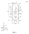
- Fig. 5 is a plan view schematically showing the vertical cavity surface emitting laser 100.
- members other than the laminated body 2 and the resin layer 70 are omitted, for the sake of convenience.
- the laminated body 2 and the resin layer 70 will be described in detail with reference to Fig. 5 .
- a length Y2 of the laminated body 2 in the Y axis direction is greater than a length X2 of the laminated body 2 in the X axis direction.
- the length Y2 of the laminated body 2 in the Y axis direction is, for example, the greatest length along the length Y2 of the laminated body 2.
- the length Y2 of the laminated body 2 is a distance in the Y axis direction between an end portion E2a of the first distortion imparting portion 2a on the positive Y axis direction side and an end portion E2b of the second distortion imparting portion 2b on the negative Y axis direction side.
- the length X2 of the laminated body 2 in the X axis direction is, for example, the greatest length along the length X2 of the laminated body 2.
- the length X2 of the laminated body 2 is a length of the resonance portion 2c in the X axis direction.
- a length Y70 of the resin layer 70 in the Y axis direction is greater than a length X70 of the resin layer 70 in the X axis direction.
- the length Y70 of the resin layer 70 in the Y axis direction is, for example, the greatest length along the length Y70 of the resin layer 70 in the Y axis direction.
- the length Y70 of the resin layer 70 is a distance in the Y axis direction between an end portion of a first curve C1 on the positive Y axis direction side and an end portion of a second curve C2 on the negative Y axis direction side.
- the length X70 of the resin layer 70 in the X axis direction is, for example, the greatest length along the length X70 of the resin layer 70 in the X axis direction.
- the length X70 of the resin layer 70 is a distance in the X axis direction between a first straight line S1 and a second straight line S2.
- the longitudinal direction of the laminated body 2 and the longitudinal direction of the resin layer 70 are the same direction (Y axis direction). Accordingly, in the vertical cavity surface emitting laser 100, it is possible to stabilize the polarization direction of the laser light. The reason thereof will be described later.
- the length of the resonance portion 2c in the X axis direction is greater than the length of the first distortion imparting portion 2a in the X axis direction or the length of the second distortion imparting portion 2b in the X axis direction.
- the length of the resonance portion 2c in the X axis direction is, for example, the greatest length along the length of the resonance portion 2c in the X axis direction.
- the length of the first distortion imparting portion 2a in the X axis direction is, for example, the greatest length along the length of the first distortion imparting portion 2a in the X axis direction.
- the length of the second distortion imparting portion 2b in the X axis direction is, for example, the greatest length along the length of the second distortion imparting portion 2b in the X axis direction.
- the first curve C1 is positioned on the positive Y axis direction side of the resonance portion 2c and the second curve C2 is positioned on the negative Y axis direction side of the resonance portion 2c.
- the outer rim of the resin layer 70 is, for example, a rim of the outermost side of the resin layer 70.
- the second distortion imparting portion 2b and the second curve C2 are positioned on the same side (negative Y axis direction side) when seen from the resonance portion 2c.
- a plan view when an end of the first straight line S1 coming in contact with the second curve C2 is set as a third end E3, an end of the second straight line S2 coming in contact with the second curve C2 is set as a fourth end E4, and a virtual straight line L E3-E4 passing through the third end E3 and the fourth end E4 is drawn, the end portion E2b of the second distortion imparting portion 2b is positioned on the resonance portion 2c side (positive Y axis direction side) when seen from the virtual straight line L E3-E4 .
- the second distortion imparting portion 2b does not intersect with the virtual straight line L E3-E4 .
- the end portion E2b of the second distortion imparting portion 2b can also be referred to as an end of the laminated body 2 on the negative Y axis direction side.
- the resin layer 70 has a shape line-symmetrical with respect to a virtual straight line (third virtual straight line) L O2c X in the X axis direction passing through a center O 2c of the resonance portion 2c.
- the resin layer 70 has a shape line-symmetrical with respect to a virtual straight line L O2c Y in the Y axis direction passing through the center O 2c of the resonance portion 2c.
- a planar shape of the resin layer 70 is not particularly limited, as long as it is a shape having a longitudinal direction.
- the planar shape of the resin layer 70 for example, may be a rectangle having a long side parallel to the Y axis direction.
- the planar shape of the resin layer 70 for example, may not be a shape line-symmetrical with respect to the virtual straight line L O2c X or L O2c Y.
- the center O 2c of the resonance portion 2c and the center O 70 of the resin layer 70 may not coincide with each other.
- a planar shape of the vertical cavity surface emitting laser 100 is a rectangle (including a square), and is configured with two sides parallel to the [110] direction and two sides parallel to the [1-10] direction.
- the longitudinal direction of the resin layer 70 and the longitudinal direction of the laminated body 2 are not limited to the [110] direction, and can be, for example, the ⁇ 110> direction.
- the longitudinal direction of the laminated body 2 can be the ⁇ 110> direction.
- the planar shape of the opening 43 of the current constriction layer 42 (see Fig. 3 ) can be respectively symmetrical about an axis which passes through the center of the opening 43 and is parallel to the X axis and an axis which passes through the center of the opening 43 and is parallel to the Y axis.
- the current constriction layer 42 is formed by oxidizing a semiconductor layer (layer to be oxidized 42a which will be described later) from the side surface of the laminated body 2.
- a semiconductor layer layer to be oxidized 42a which will be described later
- an oxidation rate in the ⁇ 100> direction is high.
- a planar shape of the opening 43 of the current constriction layer 42 is formed by tracing the shape of the outer rim of the laminated body 2 in the [100] direction, the [010] direction, the [-100] direction, and the [0-10] direction, when seen from the center of the opening 43.
- the planar shape of the opening 43 is not the shape respectively symmetrical about an axis which passes through the center of the opening 43 and is parallel to the X axis and an axis which passes through the center of the opening 43 and is parallel to the Y axis and becomes an irregular shape.
- the planar shape of the opening 43 of the current constriction layer 42 is a rhombus having a diagonal line parallel to the Y axis direction which is longer than a diagonal line parallel to the X axis direction.
- the planar shape of the opening 43 of the current constriction layer 42 may be a rhombus having angles or sides having a curvature.
- the crystal plane orientation is not particularly limited, as long as the longitudinal direction of the resin layer 70 and the longitudinal direction of the laminated body 2 coincide with each other.
- the AlGaAs vertical cavity surface emitting laser has been described, but GaInP, ZnSSe, InGaN, AlGaN, InGaAs, GaInNAs, or GaAsSb semiconductor materials may be used according to the oscillation wavelength, for the vertical cavity surface emitting laser according to the invention.
- the vertical cavity surface emitting laser 100 for example, has the following characteristics.
- the length Y2 of the laminated body 2 in the Y axis direction is greater than the length X2 of the laminated body 2 in the X axis direction, in a plan view
- the length Y70 of the resin layer 70 in the Y axis direction is greater than the length X70 of the resin layer 70 in the X axis direction, in a plan view. Accordingly, in the vertical cavity surface emitting laser 100, the stress can be applied to the active layer 30 by both of the distortion imparting portions 2a and 2b and the resin layer 70, and it is possible to stabilize the polarization direction of the laser light (see experimental examples which will be described later). Therefore, it is possible to further stabilize the polarization direction of the laser light, compared to a case where the stress is applied to the active layer 30 by only the resin layer 70 (or distortion imparting portions 2a and 2b), for example.
- the vertical cavity surface emitting laser 100 since it is possible to stabilize the polarization direction of the laser light, it is possible to stably emit circularly polarized light to the gas cell through a ⁇ /4 plate, when the vertical cavity surface emitting laser 100 is used as a light source of the atomic oscillator, for example. As a result, it is possible to increase frequency stability of the atomic oscillator. For example, when the polarization direction of the laser light emitted from the vertical cavity surface emitting laser is not stable, the light obtained through the ⁇ /4 plate may be elliptically polarized light or a rotation direction of the circularly polarized light may be fluctuated.
- the vertical cavity surface emitting laser 100 since it is possible to stabilize the polarization direction of the laser light, it is possible to stably emit the circularly polarized light to the gas cell through the ⁇ /4 plate, and to increase the frequency stability of the atomic oscillator.
- the outer rim of the resin layer 70 includes the first straight line S1, the second straight line S2 facing the first straight line S1, the first curve C1 which connects the first straight line S1 and the second straight line S2 to each other, and the second curve C2 which faces the first curve C1 and connects the first straight line S1 and the second straight line S2 to each other. Accordingly, the stress is not concentrated on the portion where the first straight line S1, the second straight line S2, and the first curve C1 are connected to each other, compared to a case where the first curve C1 has a straight line shape. Therefore, cracks hardly occur in the portion described above. In addition, cracks hardly occur in a portion where the first straight line S1, the second straight line S2, and the second curve C2 are connected to each other, for the same reason.
- the end of the first straight line S1 coming in contact with the first curve C1 is set as the first end E1
- the end of the second straight line S2 coming in contact with the first curve C1 is set as the second end E2
- the virtual straight line L E1-E2 passing through the first end E1 and the second end E2 is drawn, in a plan view, the end portion E2a of the first distortion imparting portion 2a is positioned on the resonance portion 2c side when seen from the virtual straight line.
- the material of the resin layer 70 is polyimide.
- the polyimide is a resin which is hardened by applying heat.
- the polyimide contracts in a heating step (curing step) of hardening the polyimide.
- the polyimide contracts when returning the temperature in the heating step to a room temperature. It is possible to apply great stress with respect to the active layer 30 with this contraction of the polyimide. Accordingly, in the vertical cavity surface emitting laser 100, it is possible to stabilize the polarization direction of the laser light.
- the width of the oxide area 8 is set as W1
- the width of the upper surface 48 of the second mirror layer 40 of the first distortion imparting portion 2a is set as W2, W2/W1 ⁇ 3.3. Accordingly, in the vertical cavity surface emitting laser 100, it is possible to generate a large amount of distortion in the active layer 30 by the oxide area 8, and it is possible to stabilize the polarization direction of the laser light (see experimental examples which will be described later).
- the vertical cavity surface emitting laser 100 1.3 ⁇ W2/W1 ⁇ 2.2. Accordingly, in the vertical cavity surface emitting laser 100, it is possible to further more stabilize the polarization direction of the laser light (see experimental examples which will be described later).
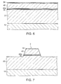
- FIGS. 6 to 9 are cross-sectional views schematically showing manufacturing steps of the vertical cavity surface emitting laser 100 according to the first embodiment, and correspond to Fig. 2 .
- the contact layer 50, the second mirror layer 40, the layer to be oxidized 42a, the active layer 30, and first mirror layer 20 are patterned to form the laminated body 2.
- the patterning is performed by photolithography or etching, for example.
- the layer to be oxidized 42a is oxidized to form the current constriction layer 42.
- the layer to be oxidized 42a is, for example, an Al x Ga 1-x As (x ⁇ 0.95) layer.
- the substrate 10 on which the laminated body 2 is formed is put in a steam atmosphere at approximately 400°C, to oxidize the Al x Ga 1-x As (x ⁇ 0.95) layer from the lateral side, and accordingly the current constriction layer 42 is formed.
- a layer configuring the first mirror layer 20 is oxidized from the lateral side to form the first area 60.
- a layer configuring the second mirror layer 40 is oxidized from the lateral side to form the second area 62.
- arsenic in the Al 0.9 Ga 0.1 As layer configuring the mirror layers 20 and 40 is substituted with oxygen, and the areas 60 and 62 are formed.
- the areas 60 and 62 for example, contract when returning the temperature from the high temperature of approximately 400°C to the room temperature, and the upper surface 63 of the second area 62 is inclined to the substrate 10 side (see Fig. 4 ).
- the first distortion imparting portion 2a and the second distortion imparting portion 2b can apply distortion (stress) caused by the contraction of the areas 60 and 62 to the active layer 30.
- the resin layer 70 is formed so as to surround the laminated body 2.
- the resin layer 70 is formed, for example, by forming a layer formed of a polyimide resin on the upper surface of the first mirror layer 20 and the entire surface of the laminated body 2 using a spin coating method and patterning the layer. The patterning is performed by photolithography or etching, for example.
- the resin layer 70 is hardened by performing a heating process (curing) .
- the resin layer 70 contracts due to the heating process.
- the resin layer 70 contracts when returning the temperature in the heating step to a room temperature.
- the second electrode 82 is formed on the contact layer 50 and the resin layer 70, and the first electrode 80 is formed on the first mirror layer 20.
- the electrodes 80 and 82 are, for example, formed by a combination of a vacuum vapor deposition method and a lift-off method.
- the order of forming the electrodes 80 and 82 is not particularly limited. In the step of forming the second electrode 82, the pad 84 and the lead-out wiring 86 (see Fig. 1 ) may be formed.
- Fig. 10 is a plan view schematically showing a vertical cavity surface emitting laser M1 according to the first experimental example.
- members other than the laminated body 2 and the resin layer 70 are omitted, for the sake of convenience.
- the longitudinal direction of the laminated body 2 and the longitudinal direction of the resin layer 70 are the Y axis direction.
- a length (width) of the first distortion imparting portion 2a and the second distortion imparting portion 2b in the X axis direction is approximately 12 ⁇ m.
- a distance between the center O 2c of the resonance portion 2c and the end portion E2a of the first distortion imparting portion 2a is approximately 50 ⁇ m.
- a diameter of the resonance portion 2c is approximately 20 ⁇ m.
- a length of the resin layer 70 in the Y axis direction is approximately 300 ⁇ m and a length of the resin layer 70 in the X axis direction is approximately 100 ⁇ m.
- the distortion imparting portions 2a and 2b are completely covered with the resin layer 70.
- the material of the resin layer 70 is polyimide.
- a configuration of the vertical cavity surface emitting laser M1 is the same as the configuration of the vertical cavity surface emitting laser 100 described above.
- light output of the vertical cavity surface emitting laser M1 is measured with a polarization filter.
- a predetermined current in this experiment, 2 mA
- the light emitted from the vertical cavity surface emitting laser M1 is caused to pass through the polarization filter having a polarization transmission axis in the X axis direction, to measure the light output.
- the plurality of vertical cavity surface emitting lasers M1 are prepared and the above measurement is performed.
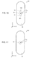
- FIGs. 11 to 13 are plan views schematically showing the vertical cavity surface emitting lasers M2, M3, and M4 according to reference examples.
- members other than the laminated body 2 and the resin layer 70 are omitted, for the sake of convenience.
- the vertical cavity surface emitting laser M2 is different from the vertical cavity surface emitting laser M1 in a point where the distortion imparting portions 2a and 2b are not provided.
- a planar shape of the laminated body 2 of the vertical cavity surface emitting laser M2 is a circle.
- the vertical cavity surface emitting laser M3 is different from the vertical cavity surface emitting laser M1 in a point where the longitudinal direction of the laminated body 2 and the longitudinal direction of the resin layer 70 are different from each other, in a plan view.
- the longitudinal direction of the laminated body 2 is the Y axis direction and the longitudinal direction of the resin layer 70 is a direction inclined with respect to the Y axis by 45 degrees.
- the center O 2c of the resonance portion 2c and the center of the resin layer 70 do not coincide with each other.
- the vertical cavity surface emitting laser M4 is different from the vertical cavity surface emitting laser M1 in a point where the longitudinal direction of the laminated body 2 and the longitudinal direction of the resin layer 70 are different from each other, in a plan view.
- the longitudinal direction of the laminated body 2 is the X axis direction
- the longitudinal direction of the resin layer 70 is the Y axis direction.
- the vertical cavity surface emitting lasers M2, M3, and M4 have the same configuration as the vertical cavity surface emitting laser M1, except for the above points.
- the light output is also measured in regards to the vertical cavity surface emitting lasers M2, M3, and M4 with the same method as in the case of the vertical cavity surface emitting laser M1.
- Fig. 14 is a histogram showing an experimental result of the vertical cavity surface emitting laser M1.
- Fig. 15 is a histogram showing an experimental result of the vertical cavity surface emitting laser M2.
- Fig. 16 is a histogram showing an experimental result of the vertical cavity surface emitting laser M3.
- Fig. 17 is a histogram showing an experimental result of the vertical cavity surface emitting laser M4.
- a horizontal axis indicates light output [mW] and a vertical axis indicates the number of elements [number].
- the largest number of elements having the light output of 1.3 mW to 1.4 mW is present, and variation in light output is slight, compared to the other vertical cavity surface emitting lasers M2, M3, and M4.
- the light output is approximately at 1.4 mW. Accordingly, in this experimental example, most of the emitted laser light of the elements having the light output of approximately 1.4 mW is not absorbed by the polarization filter and penetrate therethrough. That is, it can be said that the laser light of the elements having the light output of approximately 1.4 mW is polarized only in the X axis direction. In addition, it can be said that the laser light of the elements having the light output of 0 mW is polarized only in the Y axis direction.
- the vertical cavity surface emitting laser M1 can stably emit the laser light polarized in the X axis direction.
- the largest number of elements having the light output of 0 mW to 0.1 mW is present, but the peak is also at the light output of 1.3 mW to 1.4 mW, and the variation in light output is great, compared to the vertical cavity surface emitting laser M1. Accordingly, it is found that the polarization direction of the laser light of the vertical cavity surface emitting laser M2 is not stabilized.
- the variation in light output is found. Accordingly, it is found that the polarization direction of the laser light of the vertical cavity surface emitting laser M3 is not stabilized.
- the peaks are at the light output of 0 mW to 0.1 mW and 1.3 mW to 1.4 mW. Accordingly, it is found that the polarization direction of the laser light of the vertical cavity surface emitting laser M4 is stabilized in two directions of the X axis direction and the Y axis direction. That is, it can be said that the laser light of the vertical cavity surface emitting laser M4 is stabilized in both directions.
- the polarization direction is stabilized in one direction when the longitudinal direction of the laminated body 2 and the longitudinal direction of the resin layer 70 are the same direction.
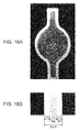
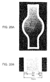
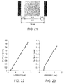
- Figs. 18A to 21 are photographs showing laminated bodies of the types A to D and are imaged using a confocal laser microscope.
- Figs. 18A , 19A , and 20A show overall views of the laminated body and Figs. 18B , 19B , and 20B show enlarged views of the distortion imparting portion of the laminated body.
- the width of the distortion imparting portion is 6 ⁇ m and the ratio W2/W1 is 1.3.
- the width of the distortion imparting portion is 8 ⁇ m and the ratio W2/W1 is 2.2.
- the width of the distortion imparting portion is 10 ⁇ m and the ratio W2/W1 is 3.3.
- the width of the distortion imparting portion is 12 ⁇ m and the ratio W2/W1 is 4.3.
- the configuration of the vertical cavity surface emitting lasers used in this experimental example is the same as the configuration of the vertical cavity surface emitting laser 100 described above.
- the light output of the types A to D is measured with the polarization filter. Specifically, the current of approximately 0 mA to 2.5 mA is supplied to the vertical cavity surface emitting laser types A to D and the light emitted from the types A to D is caused to pass through the polarization filter having a polarization transmission axis in the X axis direction, to measure the light output. The plurality of each of the types A to D are prepared and the above measurement is performed.
- the vertical cavity surface emitting laser of which the output becomes great as the current value becomes great is determined as a functional product.
- the vertical cavity surface emitting laser having a portion where the output does not become great in the example shown in Fig. 23 , an area with the current value of 0 mA to 0.6 mA) even when the current value becomes great, is determined as a defective product.
- the vertical cavity surface emitting laser having a portion where the output does not become great in the example shown in Fig. 23 , an area with the current value of 0 mA to 0.6 mA
- the emitted light is not polarized in the X axis direction in the area with the current value of 0 mA to 0.6 mA, and the emitted light is polarized in the X axis direction in an area with the current value equal to or greater than 0.6 mA. That is, in the example as shown in Fig. 23 , it can be said that the polarization direction is not stable.
- Table 1 shows the number of defective products of the types A to D.
- Table 1 Type Width of distortion imparting portion [ ⁇ m] W2/W1 Measurement number Number of defective products A 6 1.3 60 0 B 8 2.2 56 0 C 10 3.3 78 11 D 12 4.3 78 53
- Fig. 24 is a plan view schematically showing a vertical cavity surface emitting laser 200 according to the first modification example.
- members other than the laminated body 2 and the resin layer 70 are omitted, for the sake of convenience.
- the members having the same functions as the constituent members of the vertical cavity surface emitting laser 100 described above use the same reference numerals, and the specific description thereof will be omitted.
- the vertical cavity surface emitting laser 200 is different from the vertical cavity surface emitting laser 100 in a point where the resin layer 70 does not have a shape line-symmetrical with respect to the virtual straight line L O2c X in the X axis direction passing through the center O 2c of the resonance portion 2c, in a plan view.
- the resin layer 70 has a shape line-symmetrical with respect to a virtual straight line L O70 X, and the virtual straight line L O70 X is positioned on the positive Y axis direction side of the virtual straight line L O2c X.
- the center O 70 of the resin layer 70 and the center O 2c of the resonance portion 2c do not coincide with each other.
- the vertical cavity surface emitting laser 200 it is possible to stabilize the polarization direction of the laser light, in the same manner as in the vertical cavity surface emitting laser 100. (Refer to the following experimental examples.)
- Fig. 25 is a plan view schematically showing a vertical cavity surface emitting laser M5 according to the experimental example.
- members other than the laminated body 2 and the resin layer 70 are omitted, for the sake of convenience.
- the vertical cavity surface emitting laser M5 is different from the vertical cavity surface emitting laser M1 shown in Fig. 10 in a point where the resin layer 70 does not have a shape line-symmetrical with respect to the virtual straight line L O2c X in the X axis direction passing through the center O 2c of the resonance portion 2c, in a plan view.
- the vertical cavity surface emitting laser M5 has the same configuration as the vertical cavity surface emitting laser M1, except for the above points.
- the light output of the vertical cavity surface emitting laser M5 is measured with the polarization filter, in the same manner as the first experimental example.
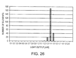
- Fig. 26 is a histogram showing an experimental result of the vertical cavity surface emitting laser M5.
- a horizontal axis indicates light output [mW] and a vertical axis indicates the number of elements [number].
- the vertical cavity surface emitting laser M5 in the vertical cavity surface emitting laser M5, the largest number of elements having the light output of 1.3 mW to 1.4 mW is present, and the variation in light output is slight, compared to the vertical cavity surface emitting lasers M2, M3, and M4 according to the reference examples.
- the degree of the variation is the same as that of the vertical cavity surface emitting laser M1.
- the vertical cavity surface emitting laser M5 can stably emit the laser light polarized in the X axis direction.
- the polarization direction is stabilized in one direction, as long as the longitudinal direction of the laminated body 2 and the longitudinal direction of the resin layer 70 are the same direction.
- Fig. 27 is a cross-sectional view schematically showing a vertical cavity surface emitting laser 201 according to the second modification example and corresponds to Fig. 2 .
- the points of the vertical cavity surface emitting laser 201 different from the example of the vertical cavity surface emitting laser 100 described above will be described, and the overlapped description will be omitted.
- the side surface of the laminated body 2 is inclined with respect to the upper surface of the substrate 10. Meanwhile, as shown in Fig. 27 , in the vertical cavity surface emitting laser 201, the side surface of the laminated body 2 is vertical to the upper surface of the substrate 10.
- the vertical cavity surface emitting laser 201 it is possible to stabilize the polarization direction of the laser light, in the same manner as the vertical cavity surface emitting laser 100.
- Figs. 28 and 29 are plan views schematically showing a vertical cavity surface emitting laser 300 according to the second embodiment.
- members other than the laminated body 2 of the vertical cavity surface emitting laser 300 are omitted.
- the members having the same functions as the constituent members of the vertical cavity surface emitting laser 100 described above use the same reference numerals, and the specific description thereof will be omitted.
- the vertical cavity surface emitting laser 300 is different from the vertical cavity surface emitting laser 100 described above, in a point where the planar shape of the laminated body 2 is an ellipse.
- the length Y2 of the laminated body 2 in the Y axis direction is greater than the length X2 thereof in the X axis direction. That is, in a plan view, the laminated body 2 has a shape having a longitudinal direction in the Y axis direction.
- the planar shape of the laminated body 2 is an ellipse including a long axis a and a short axis b, the long axis a is in parallel with the Y axis direction, and the short axis b is in parallel with the X axis direction.
- Fig. 30 is a plan view schematically showing a modification example of the vertical cavity surface emitting laser 300. In Fig. 30 , members other than the laminated body 2 are omitted.
- the planar shape of the laminated body 2 may be a rectangle (excluding a square). As shown in Fig. 30 , in a plan view, the length Y2 of the laminated body 2 in the Y axis direction is greater than the length X2 thereof in the X axis direction. That is, in a plan view, the laminated body 2 has a shape having a longitudinal direction in the Y axis direction. In the example shown in Fig. 30 , the planar shape of the laminated body 2 is a rectangle, a long side of the rectangle is in parallel with the Y axis direction, and a short side of the rectangle is in parallel with the X axis direction.
- the laminated body 2 has a shape in which the resonance portion 2c has a longitudinal direction in the Y axis direction without providing the distortion imparting portions 2a and 2b (see Fig. 3 ), the anisotropic stress (distortion) is applied to the active layer 30.
- the length Y2 of the laminated body 2 in the Y axis direction is greater than the length X2 of the laminated body 2 in the X axis direction
- the length Y70 of the resin layer 70 in the Y axis direction is greater than the length X70 of the resin layer 70 in the X axis direction.
- the length Y2 of the laminated body 2 in the Y axis direction is greater than the length X2 of the laminated body 2 in the X axis direction, it is possible to apply the anisotropic stress to the active layer 30.
- the stress generated by the shape of the laminated body 2 and the stress generated by the resin layer 70 can be applied to the active layer 30, and it is possible to stabilize the polarization direction of the laser light. Therefore, it is possible to further stabilize the polarization direction of the laser light, compared to a case where the stress is applied to the active layer 30 only by the resin layer 70.
- the manufacturing method of the vertical cavity surface emitting laser 300 is the same as the manufacturing method of the vertical cavity surface emitting laser 100 described above, and therefore the description thereof will be omitted.
- Fig. 31 is a functional block diagram of an atomic oscillator 1000 according to the third embodiment.
- the optical module 1100 includes the vertical cavity surface emitting laser according to the invention (in the example shown in the drawing, the vertical cavity surface emitting laser 100), a gas cell 1110, and a light detection unit 1120.
- Fig. 32 is a view showing frequency spectra of light emitted by the vertical cavity surface emitting laser 100.
- Fig. 33 is a view showing a relationship between ⁇ -shaped three level models of an alkaline metal atom, a first sideband wave W1, and a second sideband wave W2.
- a difference in frequencies between the frequency f 1 of the first sideband wave W1 and the frequency f 2 of the second sideband wave W2 coincides with a frequency corresponding to a difference in energy ⁇ E 12 between a ground level GL1 and a ground level GL2 of the alkaline metal atom. Accordingly, the alkaline metal atom causes an EIT phenomenon to occur due to the first sideband wave W1 including the frequency f 1 and the second sideband wave W2 including the frequency f 2 .
- a gaseous alkaline metal atom (sodium atom, rubidium atom, cesium atom, and the like) is sealed in a container.
- the alkaline metal atom causes the EIT phenomenon to occur.
- the alkaline metal atom is a sodium atom
- the frequency corresponding to the difference in energy between the ground level GL1 and the ground level GL2 in a D1 line is 9.19263... GHz. Accordingly, when two light waves including the difference in frequency of 9.19263... GHz are emitted, the EIT phenomenon occurs.
- the light detection unit 1120 detects the intensity of the light penetrating the alkaline metal atom sealed in the gas cell 1110.
- the light detection unit 1120 outputs a detection signal according to the amount of the light penetrating the alkaline metal atom.
- a photodiode is used, for example.
- the center wavelength control unit 1200 generates driving current having a magnitude corresponding to the detection signal output by the light detection unit 1120, supplies the driving current to the vertical cavity surface emitting laser 100, and controls the center wavelength ⁇ 0 of the light emitted by the vertical cavity surface emitting laser 100.
- the center wavelength ⁇ 0 of the laser light emitted by the vertical cavity surface emitting laser 100 is minutely adjusted and stabilized, by a feedback loop passing through the vertical cavity surface emitting laser 100, the gas cell 1110, the light detection unit 1120, and the center wavelength control unit 1200.
- the high frequency control unit 1300 controls so that the difference in wavelengths (frequencies) between the first sideband wave W1 and the second sideband wave W2 is equivalent to the frequency corresponding to the difference in energy between two ground levels of the alkaline metal atom sealed in the gas cell 1110, based on the detection result output by the light detection unit 1120.
- the high frequency control unit 1300 generates a modulation signal including a modulation frequency f m (see Fig. 32 ) according to the detection result output by the light detection unit 1120.
- Feedback control is performed so that the difference in frequencies between the first sideband wave W1 and the second sideband wave W2 is extremely accurately equivalent to the frequency corresponding to the difference in energy between two ground levels of the alkaline metal atom, by a feedback loop passing through the vertical cavity surface emitting laser 100, the gas cell 1110, the light detection unit 1120, and the high frequency control unit 1300.
- the modulation frequency f m becomes an extremely stabilized frequency, and therefore, the modulation signal can be set as an output signal (clock output) of the atomic oscillator 1000.
- the laser light emitted from the vertical cavity surface emitting laser 100 is incident to the gas cell 1110.
- the light emitted from the vertical cavity surface emitting laser 100 includes two light waves (the first sideband wave W1 and the second sideband wave W2) including the frequency (wavelength) corresponding to the difference in energy between two ground levels of the alkaline metal atom, and the alkaline metal atom causes the EIT phenomenon to occur.
- the intensity of the light penetrating the gas cell 1110 is detected by the light detection unit 1120.
- the center wavelength control unit 1200 and the high frequency control unit 1300 perform the feedback control so that the difference in frequencies between the first sideband wave W1 and the second sideband wave W2 extremely accurately coincides with the frequency corresponding to the difference in energy between two ground levels of the alkaline metal atom.
- a rapid change in a light absorbing behavior when the difference in frequencies f 1 -f 2 between the first sideband wave W1 and the second sideband wave W2 is deviated from the frequency corresponding to the difference in energy ⁇ E 12 between the ground level GL1 and the ground level GL2 is detected and controlled using the EIT phenomenon, and therefore it is possible to obtain an oscillator with high accuracy.
- the invention has configurations substantially same as the configurations described in the embodiments (for example, configurations with the same function, method, and effects, or configurations with the same object and effect).
- the invention includes a configuration in which non-essential parts of the configurations described in the embodiments are replaced.
- the invention includes a configuration having the same operation effect as the configurations described in the embodiments or a configuration which can achieve the same object.
- the invention includes a configuration obtained by adding a well-known technology to the configurations described in the embodiments.
Landscapes
- Physics & Mathematics (AREA)
- General Physics & Mathematics (AREA)
- Condensed Matter Physics & Semiconductors (AREA)
- Electromagnetism (AREA)
- Optics & Photonics (AREA)
- Life Sciences & Earth Sciences (AREA)
- Ecology (AREA)
- Semiconductor Lasers (AREA)
Abstract
Description
- The present invention relates to a vertical cavity surface emitting laser and an atomic oscillator.
- The vertical cavity surface emitting laser (VCSEL) is, for example, used as a light source of the atomic oscillator using coherent population trapping (CPT) which is one of the quantum interference effects.
- In the vertical cavity surface emitting laser, a resonator generally has an isotropic structure, and accordingly it is difficult to control a polarization direction of laser light emitted from the resonator.
JP-A-2001-189525 - However, in the vertical cavity surface emitting laser disclosed in
JP-A-2001-189525 - An advantage of some aspects of the invention is to provide a vertical cavity surface emitting laser which can stabilize a polarization direction of laser light. In addition, another advantage of some aspects of the invention is to provide an atomic oscillator including the vertical cavity surface emitting laser.
- An aspect of the invention is directed to a vertical cavity surface emitting laser including: a substrate; a laminated body which is provided over the substrate; and a resin layer which is provided on at least a side surface of the laminated body, in which the laminated body at least includes a first mirror layer provided over the substrate, an active layer provided over the first mirror layer, and a second mirror layer provided over the active layer, in a plan view, a length of the laminated body in a first direction is greater than a length of the laminated body in a second direction orthogonal to the first direction, and in the plan view, a length of the resin layer in the first direction is greater than a length of the resin layer in the second direction.
- According to the vertical cavity surface emitting laser, since the length of the laminated body in the first direction is greater than the length of the laminated body in the second direction in a plan view, it is possible to apply anisotropic stress to the active layer. Accordingly, in the vertical cavity surface emitting laser, stress generated by the shape of the laminated body and stress generated by the resin layer can be applied to the active layer, and it is possible to stabilize a polarization direction of laser light. Therefore, it is possible to further stabilize the polarization direction of the laser light, compared to a case where the stress is applied to the active layer only by the resin layer.
- In the description according to the invention, for example, when a phrase "over" is used in a sentence such as "to form a specific element (hereinafter, referred to as a "B") over another specific element (hereinafter, referred to as an "A")", the phrase "over" is used to include a case of forming the B directly on the A and a case of forming the B on the A with another element interposed therebetween.
- In the vertical cavity surface emitting laser according to the aspect of the invention, in the plan view, the laminated body may include a first portion, a second portion, and a third portion provided between the first portion and the second portion, the first portion and the second portion may face each other in the first direction, and in the plan view, a length of the third portion in the second direction may be greater than a length of the first portion or a length of the second portion in the second direction.
- According to the vertical cavity surface emitting laser with this configuration, since the laminated body includes the first portion and the second portion, it is possible to apply the stress to the third portion. Accordingly, in the vertical cavity surface emitting laser, stress generated by the first portion and the second portion and stress generated by the resin layer can be applied to the active layer, and it is possible to stabilize the polarization direction of the laser light.
- In the vertical cavity surface emitting laser according to the aspect of the invention, in the plan view, an outer rim of the resin layer may include a first straight line, a second straight line facing the first straight line, a first curve which connects the first straight line and the second straight line to each other, and a second curve which faces the first curve and connects the first straight line and the second straight line to each other.
- According to the vertical cavity surface emitting laser with this configuration, the stress is not concentrated on a portion where the first straight line, the second straight line, and the first curve are connected to each other, compared to a case where the first curve has a straight line shape. Therefore, cracks hardly occur in the portion described above. In addition, cracks hardly occur in a portion where the first straight line, the second straight line, and the second curve are connected to each other, for the same reason.
- In the vertical cavity surface emitting laser according to the aspect of the invention, in the plan view, the first portion and the first curve may be positioned on the same side when seen from the third portion, and in the plan view, when an end of the first straight line coming in contact with the first curve is set as a first end, an end of the second straight line coming in contact with the first curve is set as a second end, and a first virtual straight line passing through the first end and the second end is drawn, an end portion of the first portion may be positioned on the third portion side, when seen from the first virtual straight line.
- According to the vertical cavity surface emitting laser with this configuration, even if cracks occur in the portion where the first straight line, the second straight line, and the first curve are connected to each other, since the end portion of the first portion is positioned on the third portion side which is the inner side with respect to the portion described above, it is possible to suppress the cracks reaching the first portion. Therefore, it is possible to increase protection performance with respect to the laminated body.
- In the vertical cavity surface emitting laser according to the aspect of the invention, the laminated body may further include a current constriction layer provided between the first mirror layer and the second mirror layer, a first area including a plurality of oxide layers provided to be connected to the first mirror layer, and a second area including a plurality of oxide layers provided to be connected to the second mirror layer, in the plan view, an oxide area may be configured with the first area and the second area of the first portion of the laminated body, and in the plan view, when a width of the oxide area is set as W1 and a width of an upper surface of the second mirror layer of the first portion is set as W2, the relationship of W2/W1 ≤ 3.3 may be satisfied.
- According to the vertical cavity surface emitting laser with this configuration, it is possible to generate a large amount of distortion in the active layer by the oxide area, and it is possible to stabilize the polarization direction of the laser light (this will be described later in detail).
- In the vertical cavity surface emitting laser according to the aspect of the invention, the relationship of W2/W1 ≤ 2.2 may be satisfied.
- According to the vertical cavity surface emitting laser with this configuration, it is possible to furthermore stabilize the polarization direction of the laser light.
- In the vertical cavity surface emitting laser according to the aspect of the invention, the relationship of 1.3 ≤ W2/W1 may be satisfied.
- According to the vertical cavity surface emitting laser with this configuration, it is possible to further more stabilize the polarization direction of the laser light.
- In the vertical cavity surface emitting laser according to the aspect of the invention, in the plan view, when a second virtual straight line orthogonal to the first direction is drawn on the first portion, the W2 which is the width of the upper surface of the second mirror layer may be positioned on the second virtual straight line.
- According to the vertical cavity surface emitting laser with this configuration, it is possible to stabilize the polarization direction of the laser light.
- In the vertical cavity surface emitting laser according to the aspect of the invention, in the plan view, a first portion and a second portion of the oxide area may be provided in a position overlapped with the second virtual straight line so as to interpose the upper surface of the second mirror layer therebetween, W1 which is the width of the oxide area may be a width of the first portion of the oxide area, and W1 which is the width of the oxide area may be positioned on the second virtual straight line.
- According to the vertical cavity surface emitting laser with this configuration, it is possible to stabilize the polarization direction of the laser light.
- In the vertical cavity surface emitting laser according to the aspect of the invention, the laminated body may further include a current constriction layer provided between the first mirror layer and the second mirror layer, a first area including a plurality of oxide layers provided to be connected to the first mirror layer, and a second area including a plurality of oxide layers provided to be connected to the second mirror layer, in a cross-sectional view, the lowest oxide layer among the plurality of oxide layers in the first area may include a first end facing an end which comes in contact with the first mirror layer of the first portion, in the cross-sectional view, the highest oxide layer among the plurality of oxide layers in the second area may include a second end which comes in contact with the second mirror layer of the first portion, and in the plan view, when a width from the first end to the second end is set as W1 and a width of an upper surface of the second mirror layer of the first portion is set as W2, the relationship of W2/W1 ≤ 3.3 may be satisfied.
- According to the vertical cavity surface emitting laser with this configuration, it is possible to generate a large amount of distortion in the active layer by the oxide layer, and it is possible to stabilize the polarization direction of the laser light.
- In the vertical cavity surface emitting laser according to the aspect of the invention, the relationship of W2/W1 ≤ 2.2 may be satisfied.
- According to the vertical cavity surface emitting laser with this configuration, it is possible to further more stabilize the polarization direction of the laser light.
- In the vertical cavity surface emitting laser according to the aspect of the invention, the relationship of 1.3 ≤ W2/W1 may be satisfied.
- According to the vertical cavity surface emitting laser with this configuration, it is possible to further more stabilize the polarization direction of the laser light.
- In the vertical cavity surface emitting laser according to the aspect of the invention, in the plan view, when a second virtual straight line orthogonal to the first direction is drawn on the first portion, the W2 which is the width of the upper surface of the second mirror layer may be positioned on the second virtual straight line.
- According to the vertical cavity surface emitting laser with this configuration, it is possible to stabilize the polarization direction of the laser light.
- In the vertical cavity surface emitting laser according to the aspect of the invention, in the cross-sectional view, a first portion and a second portion of the first area may be provided so as to interpose the first mirror layer of the first portion of the laminated body, in the cross-sectional view, a first portion of the second area may be provided over the first portion of the first area and a second portion of the second area may be provided over the second portion of the first area, so as to interpose the second mirror layer of the first portion of the laminated body, the first portion of the first area may include the lowest oxide layer, the first portion of the second area may include the highest oxide layer, and W1 which is a width from the first end of the lowest oxide layer to the second end of the highest oxide layer may be positioned on the second virtual straight line.
- According to the vertical cavity surface emitting laser with this configuration, it is possible to stabilize the polarization direction of the laser light.
- In the vertical cavity surface emitting laser according to the aspect of the invention, in the plan view, the resin layer may have a shape line-symmetrical with respect to a third virtual straight line in the second direction passing through a center of the third portion.
- According to the vertical cavity surface emitting laser with this configuration, it is possible to stabilize the polarization direction of the laser light.
- In the vertical cavity surface emitting laser according to the aspect of the invention, in the plan view, the resin layer may not have a shape line-symmetrical with respect to a third virtual straight line in the second direction passing through a center of the third portion.
- According to the vertical cavity surface emitting laser with this configuration, it is possible to stabilize the polarization direction of the laser light.
- In the vertical cavity surface emitting laser according to the aspect of the invention, in the plan view, the laminated body may further include a first distortion imparting portion, a second distortion imparting portion, and a resonance portion which is provided between the first distortion imparting portion and the second distortion imparting portion and resonates light generated by the active layer, the first distortion imparting portion and the second distortion imparting portion may face each other in the first direction, and in the plan view, a length of the resonance portion in the second direction may be greater than a length of the first distortion imparting portion or a length of the second distortion imparting portion in the second direction.
- According to the vertical cavity surface emitting laser with this configuration, since the laminated body includes the first distortion imparting portion and the second distortion imparting portion, it is possible to apply the stress to the resonance portion. Accordingly, in the vertical cavity surface emitting laser, stress generated by the first distortion imparting portion and the second distortion imparting portion and stress generated by the resin layer can be applied to the active layer, and it is possible to stabilize the polarization direction of the laser light.
- In the vertical cavity surface emitting laser according to the aspect of the invention, in the plan view, an outer rim of the resin layer may include a first straight line, a second straight line facing the first straight line, a first curve which connects the first straight line and the second straight line to each other, and a second curve which faces the first curve and connects the first straight line and the second straight line to each other.
- According to the vertical cavity surface emitting laser with this configuration, the stress is not concentrated on a portion where the first straight line, the second straight line, and the first curve are connected to each other, compared to a case where the first curve has a straight line shape. Therefore, cracks hardly occur in the portion described above. In addition, cracks hardly occur in a portion where the first straight line, the second straight line, and the second curve are connected to each other, for the same reason.
- In the vertical cavity surface emitting laser according to the aspect of the invention, in the plan view, the first distortion imparting portion and the first curve may be positioned on the same side when seen from the resonance portion, and in the plan view, when an end of the first straight line coming in contact with the first curve is set as a first end, an end of the second straight line coming in contact with the first curve is set as a second end, and a first virtual straight line passing through the first end and the second end is drawn, an end portion of the first distortion imparting portion may be positioned on the resonance portion side, when seen from the first virtual straight line.
- According to the vertical cavity surface emitting laser with this configuration, even if cracks occur in the portion where the first straight line, the second straight line, and the first curve are connected to each other, since the end portion of the first distortion imparting portion is positioned on the third portion side which is the inner side with respect to the portion described above, it is possible to suppress the cracks reaching the first distortion imparting portion. Therefore, it is possible to increase protection performance with respect to the laminated body.
- In the vertical cavity surface emitting laser according to the aspect of the invention, the laminated body may further include a current constriction layer provided between the first mirror layer and the second mirror layer, a first area including a plurality of oxide layers provided to be connected to the first mirror layer, and a second area including a plurality of oxide layers provided to be connected to the second mirror layer, in the plan view, an oxide area may be configured with the first area and the second area of the first distortion imparting portion of the laminated body, and in the plan view, when a width of the oxide area is set as W1 and a width of an upper surface of the second mirror layer of the first distortion imparting portion is set as W2, the relationship of W2/W1 ≤ 3.3 may be satisfied.
- According to the vertical cavity surface emitting laser with this configuration, it is possible to generate a large amount of distortion in the active layer by the oxide area, and it is possible to stabilize the polarization direction of the laser light (this will be described later in detail).
- In the vertical cavity surface emitting laser according to the aspect of the invention, the relationship of W2/W1 ≤ 2.2 may be satisfied.
- According to the vertical cavity surface emitting laser with this configuration, it is possible to further more stabilize the polarization direction of the laser light.
- In the vertical cavity surface emitting laser according to the aspect of the invention, the relationship of 1.3 ≤ W2/W1 may be satisfied.
- According to the vertical cavity surface emitting laser with this configuration, it is possible to further more stabilize the polarization direction of the laser light.
- In the vertical cavity surface emitting laser according to the aspect of the invention, in the plan view, when a second virtual straight line orthogonal to the first direction is drawn on the first distortion imparting portion, the W2 which is the width of the upper surface of the second mirror layer may be positioned on the second virtual straight line.
- According to the vertical cavity surface emitting laser with this configuration, it is possible to stabilize the polarization direction of the laser light.
- In the vertical cavity surface emitting laser according to the aspect of the invention, in the plan view, a first portion and a second portion of the oxide area may be provided in a position overlapped with the second virtual straight line so as to interpose the upper surface of the second mirror layer therebetween, the W1 which is the width of the oxide area may be a width of the first portion of the oxide area, and the W1 which is the width of the oxide area may be positioned on the second virtual straight line.
- According to the vertical cavity surface emitting laser with this configuration, it is possible to stabilize the polarization direction of the laser light.
- In the vertical cavity surface emitting laser according to the aspect of the invention, the laminated body may further include a current constriction layer provided between the first mirror layer and the second mirror layer, a first area including a plurality of oxide layers provided to be connected to the first mirror layer, and a second area including a plurality of oxide layers provided to be connected to the second mirror layer, in a cross-sectional view, the lowest oxide layer among the plurality of oxide layers in the first area may include a first end facing an end which comes in contact with the first mirror layer of the first distortion imparting portion, in the cross-sectional view, the highest oxide layer among the plurality of oxide layers in the second area may include a second end which comes in contact with the second mirror layer of the first distortion imparting portion, and in the plan view, when a width from the first end to the second end is set as W1 and a width of an upper surface of the second mirror layer of the first distortion imparting portion is set as W2, the relationship of W2/W1 ≤ 3.3 may be satisfied.
- According to the vertical cavity surface emitting laser with this configuration, it is possible to generate a large amount of distortion in the active layer by the oxide area, and it is possible to stabilize the polarization direction of the laser light (this will be described later in detail).
- In the vertical cavity surface emitting laser according to the aspect of the invention, the relationship of W2/W1 ≤ 2.2 may be satisfied.
- According to the vertical cavity surface emitting laser with this configuration, it is possible to further more stabilize the polarization direction of the laser light.
- In the vertical cavity surface emitting laser according to the aspect of the invention, the relationship of 1.3 ≤ W2/W1 may be satisfied.
- According to the vertical cavity surface emitting laser with this configuration, it is possible to further more stabilize the polarization direction of the laser light.
- In the vertical cavity surface emitting laser according to the aspect of the invention, in the plan view, when a second virtual straight line orthogonal to the first direction is drawn on the first distortion imparting portion, the W2 which is the width of the upper surface of the second mirror layer may be positioned on the second virtual straight line.
- According to the vertical cavity surface emitting laser with this configuration, it is possible to stabilize the polarization direction of the laser light.
- In the vertical cavity surface emitting laser according to the aspect of the invention, in the cross-sectional view, a first portion and a second portion of the first area may be provided so as to interpose the first mirror layer of the first distortion imparting portion of the laminated body, in the cross-sectional view, a first portion of the second area may be provided over the first portion of the first area and a second portion of the second area may be provided over the second portion of the first area, so as to interpose the second mirror layer of the first distortion imparting portion of the laminated body, the first portion of the first area may include the lowest oxide layer, the first portion of the second area may include the highest oxide layer, and W1 which is a width from the first end of the lowest oxide layer to the second end of the highest oxide layer may be positioned on the second virtual straight line.
- According to the vertical cavity surface emitting laser with this configuration, it is possible to stabilize the polarization direction of the laser light.
- In the vertical cavity surface emitting laser according to the aspect of the invention, in the plan view, the resin layer may have a shape line-symmetrical with respect to a third virtual straight line in the second direction passing through a center of the resonance portion.
- According to the vertical cavity surface emitting laser with this configuration, it is possible to stabilize the polarization direction of the laser light.
- In the vertical cavity surface emitting laser according to the aspect of the invention, in the plan view, the resin layer may not have a shape line-symmetrical with respect to a third virtual straight line in the second direction passing through a center of the resonance portion.
- According to the vertical cavity surface emitting laser with this configuration, it is possible to stabilize the polarization direction of the laser light.
- In the vertical cavity surface emitting laser according to the aspect of the invention, a material of the resin layer may be polyimide.
- According to the vertical cavity surface emitting laser with this configuration, the resin layer can apply great stress with respect to the resonance portion (third portion) . Therefore, it is possible to stabilize the polarization direction of the laser light.
- Another aspect of the invention is directed to an atomic oscillator including: the vertical cavity surface emitting laser according to the aspect of the invention.
- According to the atomic oscillator, since the atomic oscillator includes the vertical cavity surface emitting laser according to the aspect of the invention, it is possible to stably emit circularly polarized light to the gas cell through a λ/4 plate, for example, and it is possible to increase frequency stability of the atomic oscillator.
- The invention will be described with reference to the accompanying drawings, wherein like numbers reference like elements.
-
Fig. 1 is a plan view schematically showing a vertical cavity surface emitting laser according to a first embodiment. -
Fig. 2 is a cross-sectional view schematically showing a vertical cavity surface emitting laser according to a first embodiment. -
Fig. 3 is a plan view schematically showing a vertical cavity surface emitting laser according to a first embodiment. -
Fig. 4 is a cross-sectional view schematically showing a vertical cavity surface emitting laser according to a first embodiment. -
Fig. 5 is a plan view schematically showing a vertical cavity surface emitting laser according to a first embodiment. -
Fig. 6 is a cross-sectional view schematically showing a manufacturing step of a vertical cavity surface emitting laser according to a first embodiment. -
Fig. 7 is a cross-sectional view schematically showing a manufacturing step of a vertical cavity surface emitting laser according to a first embodiment. -
Fig. 8 is a cross-sectional view schematically showing a manufacturing step of a vertical cavity surface emitting laser according to a first embodiment. -
Fig. 9 is a cross-sectional view schematically showing a manufacturing step of a vertical cavity surface emitting laser according to a first embodiment. -
Fig. 10 is a plan view schematically showing a vertical cavity surface emitting laser according to a first experimental example. -
Fig. 11 is a plan view schematically showing a vertical cavity surface emitting laser according to a reference example. -
Fig. 12 is a plan view schematically showing a vertical cavity surface emitting laser according to a reference example. -
Fig. 13 is a plan view schematically showing a vertical cavity surface emitting laser according to a reference example. -
Fig. 14 is a histogram showing an experimental result of a vertical cavity surface emitting laser according to a first experimental example. -
Fig. 15 is a histogram showing an experimental result of a vertical cavity surface emitting laser according to a reference example. -
Fig. 16 is a histogram showing an experimental result of a vertical cavity surface emitting laser according to a reference example. -
Fig. 17 is a histogram showing an experimental result of a vertical cavity surface emitting laser according to a reference example. -
Figs. 18A and 18B are photographs of a vertical cavity surface emitting laser used in a second experimental example. -
Figs. 19A and 19B are photographs of a vertical cavity surface emitting laser used in a second experimental example. -
Figs. 20A and 20B are photographs of a vertical cavity surface emitting laser used in a second experimental example. -
Fig. 21 is a photograph of a vertical cavity surface emitting laser used in a second experimental example. -
Fig. 22 is a graph showing a relationship between current and output of a functional vertical cavity surface emitting laser. -
Fig. 23 is a graph showing a relationship between current and output of a defective vertical cavity surface emitting laser. -
Fig. 24 is a plan view schematically showing a vertical cavity surface emitting laser according to a first modification example of a first embodiment. -
Fig. 25 is a plan view schematically showing a vertical cavity surface emitting laser according to the experimental example. -
Fig. 26 is a histogram showing an experimental result of a vertical cavity surface emitting laser according to the experimental example. -
Fig. 27 is a cross-sectional view schematically showing a vertical cavity surface emitting laser according to a second modification example of a first embodiment. -
Fig. 28 is a plan view schematically showing a vertical cavity surface emitting laser according to a second embodiment. -
Fig. 29 is a plan view schematically showing a vertical cavity surface emitting laser according to a second embodiment. -
Fig. 30 is a plan view schematically showing a vertical cavity surface emitting laser according to a modification example of a second embodiment. -
Fig. 31 is a functional block diagram of an atomic oscillator according to a third embodiment. -
Fig. 32 is a view showing frequency spectra of resonant light. -
Fig. 33 is a view showing a relationship between A-shaped three level models of an alkaline metal atom, a first sideband wave, and a second sideband wave. - Hereinafter, preferred embodiments of the invention will be described in detail with reference to the drawings. The embodiments described below are not intended to unduly limit the contents of the invention disclosed in the aspects. All of the configurations described below are not limited to be essential constituent elements of the invention.
- First, a vertical cavity surface emitting laser according to a first embodiment will be described with reference to the drawings.
Fig. 1 is a plan view schematically showing a vertical cavitysurface emitting laser 100 according to the first embodiment.Fig. 2 is a cross-sectional view which is taken along line II-II ofFig. 1 and schematically shows the vertical cavitysurface emitting laser 100 according to the first embodiment.Fig. 3 is a plan view schematically showing the vertical cavitysurface emitting laser 100 according to the first embodiment.Fig. 4 is a cross-sectional view which is taken along line IV-IV ofFig. 3 and schematically shows the vertical cavitysurface emitting laser 100 according to the first embodiment. - For the sake of convenience,
Fig. 2 shows a simplifiedlaminated body 2. InFig. 3 , members other than thelaminated body 2 of the vertical cavitysurface emitting laser 100 are omitted.Figs. 1 to 4 show an X axis, a Y axis, and a Z axis as three axes orthogonal to each other. - As shown in
Figs. 1 to 4 , the vertical cavitysurface emitting laser 100 includes asubstrate 10, afirst mirror layer 20, anactive layer 30, asecond mirror layer 40, acurrent constriction layer 42, acontact layer 50,first areas 60,second areas 62, aresin layer 70,first electrodes 80, andsecond electrodes 82. - The
substrate 10 is, for example, a first conductive (for example, n-type) GaAs substrate. - The
first mirror layer 20 is formed on thesubstrate 10. Thefirst mirror layer 20 is a first conductive semiconductor layer. As shown inFig. 4 , thefirst mirror layer 20 is a distribution Bragg reflection (DBR) type mirror in which high refractive index layers 24 and low refractive index layers 26 are laminated onto each other. The highrefractive index layer 24 is, for example, an n-type Al0.12Ga0.88As layer on which silicon is doped. The lowrefractive index layer 26 is, for example, an n-type Al0.9Ga0.1As layer on which silicon is doped. The number (number of pairs) of laminated high refractive index layers 24 and low refractive index layers 26 is, for example, 10 pairs to 50 pairs, specifically, 40.5 pairs. - The
active layer 30 is provided on thefirst mirror layer 20. Theactive layer 30, for example, has a multiple quantum well (MQW) structure in which three layers having a quantum well structure configured with an i-type In0.06Ga0.94AS layer and an i-type Al0.3Ga0.7As layer are overlapped. - The
second mirror layer 40 is formed on theactive layer 30. Thesecond mirror layer 40 is a second conductive (for example, p-type) semiconductor layer. Thesecond mirror layer 40 is a distribution Bragg reflection (DBR) type mirror in which high refractive index layers 44 and low refractive index layers 46 are laminated onto each other. The highrefractive index layer 44 is, for example, a p-type Al0.12Ga0.88As layer on which carbon is doped. The lowrefractive index layer 46 is, for example, a p-type Al0.9Ga0.1As layer on which carbon is doped. The number (number of pairs) of laminated high refractive index layers 44 and low refractive index layers 46 is, for example, 3 pairs to 40 pairs, specifically, 20 pairs. - The
second mirror layer 40, theactive layer 30, and thefirst mirror layer 20 configure a vertical resonator-type pin diode. When a forward voltage of the pin diode is applied between theelectrodes active layer 30, and the light emitting occurs. The light generated in theactive layer 30 reciprocates between thefirst mirror layer 20 and the second mirror layer 40 (multiple reflection), the induced emission occurs at that time, and the intensity is amplified. When an optical gain exceeds an optical loss, laser oscillation occurs, and the laser light is emitted in a vertical direction (a lamination direction of thefirst mirror layer 20 and the active layer 30) from the upper surface of thecontact layer 50. - The
current constriction layer 42 is provided between thefirst mirror layer 20 and thesecond mirror layer 40. In the example shown in the drawing, thecurrent constriction layer 42 is provided on theactive layer 30. Thecurrent constriction layer 42 can also be provided in thefirst mirror layer 20 or thesecond mirror layer 40. In this case as well, thecurrent constriction layer 42 is assumed to be provided between thefirst mirror layer 20 and thesecond mirror layer 40. Thecurrent constriction layer 42 is an insulation layer in which anopening 43 is formed. Thecurrent constriction layer 42 can prevent spreading of the current injected to a vertical resonator by theelectrodes first mirror layer 20 and the active layer 30). - The
contact layer 50 is provided on thesecond mirror layer 40. Thecontact layer 50 is a second conductive semiconductor layer. Specifically, thecontact layer 50 is a p-type GaAs layer on which carbon is doped. - As shown in
Fig. 4 , thefirst areas 60 are provided on lateral portions of thefirst mirror layer 20 configuring thelaminated body 2. Thefirst areas 60 include a plurality ofoxide layers 6 which are provided to be connected to the first mirror layer 20 (in the example shown in the drawing, a part of the first mirror layer 20). Specifically,first areas 60 are configured with the oxide layers 6 obtained by oxidizing layers connected to the low refractive index layers 26 (for example, Al0.9Ga0.1As layers) configuring thefirst mirror layer 20, and layers 4 connected to the high refractive index layers 24 (for example, Al0.12Ga0.88As layers) configuring thefirst mirror layer 20 which are laminated on each other. - The
second areas 62 are provided on lateral portions of thesecond mirror layer 40 configuring thelaminated body 2. Thesecond areas 62 include a plurality ofoxide layers 16 which are provided to be connected to thesecond mirror layer 40. Specifically, thesecond areas 62 are configured with the oxide layers 16 obtained by oxidizing layers connected to the low refractive index layers 46 (for example, Al0.9Ga0.1As layers) configuring thesecond mirror layer 40, and layers 14 connected to the high refractive index layers 44 (for example, Al0.12Ga0.88As layers) configuring thesecond mirror layer 40 which are laminated on each other. In a plan view (when seen from the lamination direction of thefirst mirror layer 20 and the active layer 30),oxide areas 8 are configured by thefirst areas 60 and thesecond areas 62. - The
first mirror layer 20, theactive layer 30, thesecond mirror layer 40, thecurrent constriction layer 42, thecontact layer 50, thefirst areas 60, and thesecond areas 62 configure thelaminated body 2. In the example shown inFigs. 1 and 2 , thelaminated body 2 is surrounded with theresin layer 70. - In the example shown in
Fig. 3 , in a plan view, a length of thelaminated body 2 in a Y axis direction is greater than a length of thelaminated body 2 in an X axis direction. That is, a longitudinal direction of thelaminated body 2 is the Y axis direction. In a plan view, thelaminated body 2 is, for example, symmetrical about a virtual straight line which passes through the center of thelaminated body 2 and is parallel to the X axis. In a plan view, thelaminated body 2 is, for example, symmetrical about a virtual straight line which passes through the center of thelaminated body 2 and is parallel to the Y axis. - In a plan view as shown in
Fig. 3 , thelaminated body 2 includes a first distortion imparting portion (first portion) 2a, a second distortion imparting portion (second portion) 2b, and a resonance portion (third portion) 2c. - In a plan view, the first
distortion imparting portion 2a and the seconddistortion imparting portion 2b face each other in the Y axis direction with theresonance portion 2c interposed therebetween. In a plan view, the firstdistortion imparting portion 2a is protruded from theresonance portion 2c in the positive Y axis direction. In a plan view, the seconddistortion imparting portion 2b is protruded from theresonance portion 2c in the negative Y axis direction. The firstdistortion imparting portion 2a and the seconddistortion imparting portion 2b are provided to be integrated with theresonance portion 2c. - The first
distortion imparting portion 2a and the seconddistortion imparting portion 2b impart distortion to theactive layer 30 and polarize light generated in theactive layer 30. Herein, to polarize the light is to set a vibration direction of an electric field of the light to be constant. The semiconductor layers (thefirst mirror layer 20, theactive layer 30, thesecond mirror layer 40, thecurrent constriction layer 42, thecontact layer 50, thefirst areas 60, and the second areas 62) configuring the firstdistortion imparting portion 2a and the seconddistortion imparting portion 2b are a generation source which generates distortion to be imparted to theactive layer 30. Since the firstdistortion imparting portion 2a and the seconddistortion imparting portion 2b include thefirst areas 60 including the plurality ofoxide layers 6 and thesecond areas 62 including the plurality of oxide layers 16, it is possible to impart a large amount of distortion to theactive layer 30. - The
resonance portion 2c is provided between the firstdistortion imparting portion 2a and the seconddistortion imparting portion 2b. A length of theresonance portion 2c in the X axis direction is greater than a length of the firstdistortion imparting portion 2a in the X axis direction or a length of the seconddistortion imparting portion 2b in the X axis direction. A planar shape of theresonance portion 2c (shape when seen from the lamination direction of thefirst mirror layer 20 and the active layer 30) is, for example, a circle. - The
resonance portion 2c resonates light generated in theactive layer 30. That is, the vertical oscillator is formed in theresonance portion 2c. - The
resin layer 70 is provided at least on side surfaces of thelaminated body 2. In the example shown inFig. 1 , theresin layer 70 covers the firstdistortion imparting portion 2a and the seconddistortion imparting portion 2b. That is, theresin layer 70 is provided on the side surface of the firstdistortion imparting portion 2a, the upper surface of the firstdistortion imparting portion 2a, the side surface of the seconddistortion imparting portion 2b, and the upper surface of the seconddistortion imparting portion 2b. Theresin layer 70 may completely cover the firstdistortion imparting portion 2a and the seconddistortion imparting portion 2b, or may cover some of the firstdistortion imparting portion 2a and the seconddistortion imparting portion 2b. The material of theresin layer 70 is, for example, polyimide. - In the example shown in
Fig. 3 , in a plan view, a length of theresin layer 70 in the Y axis direction is greater than a length of theresin layer 70 in the X axis direction. That is, a longitudinal direction of theresin layer 70 is the Y axis direction. The longitudinal direction of theresin layer 70 and the longitudinal direction of thelaminated body 2 coincide with each other. - The
first electrodes 80 are provided on thefirst mirror layer 20. Thefirst electrodes 80 form ohmic contact with thefirst mirror layer 20. Thefirst electrodes 80 are electrically connected to thefirst mirror layer 20. As thefirst electrodes 80, an electrode in which a Cr layer, an AuGe layer, an Ni layer, and an Au layer are laminated in this order from thefirst mirror layer 20 side is used, for example. Thefirst electrodes 80 are the electrodes for injecting the current to theactive layer 30. Although not shown, thefirst electrodes 80 may be provided on the lower surface of thesubstrate 10. - The
second electrodes 82 are provided on the contact layer 50 (on the laminated body 2). Thesecond electrodes 82 form ohmic contact with thecontact layer 50. In the example shown in the drawing, thesecond electrodes 82 are also formed on theresin layer 70. Thesecond electrodes 82 are electrically connected to thesecond mirror layer 40 through thecontact layer 50. As thesecond electrodes 82, an electrode in which a Cr layer, a Pt layer, a Ti layer, a Pt layer, and an Au layer are laminated in this order from thecontact layer 50 side is used, for example. Thesecond electrodes 82 are the other electrodes for injecting the current to theactive layer 30. - The
second electrodes 82 are electrically connected to apad 84. In the example shown in the drawing, thesecond electrodes 82 are electrically connected to thepad 84 through a lead-out wiring 86. Thepad 84 is provided on theresin layer 70. The material of thepad 84 and the lead-out wiring 86 is, for example, the same as the material of thesecond electrodes 82. - Herein, the
laminated body 2 will be described in more detail. Thelaminated body 2 includes the firstdistortion imparting portion 2a having a first width (length in the X axis direction), the seconddistortion imparting portion 2b having a second width, and theresonance portion 2c having a third width wider than the first width and the second width. In the example shown in the drawing, the first width and the second width are the same width as each other. - The first width is, for example, a maximum width along the width of the first
distortion imparting portion 2a, in a direction (X axis direction) orthogonal to a direction (Y axis direction) in which the firstdistortion imparting portion 2a and the seconddistortion imparting portion 2b face each other. The second width is, for example, a maximum width along the width of the seconddistortion imparting portion 2b, in the direction orthogonal to the direction in which the firstdistortion imparting portion 2a and the seconddistortion imparting portion 2b face each other. The third width is, for example, a maximum width along the width of theresonance portion 2c, in the direction orthogonal to the direction in which the firstdistortion imparting portion 2a and the seconddistortion imparting portion 2b face each other. - In a plan view, the
oxide area 8 is configured with thefirst area 60 and thesecond area 62 of the firstdistortion imparting portion 2a. In a plan view, when a width of the oxide area 8 (size in the X axis direction) is set as W1 and a width of an upper surface 48 of thesecond mirror layer 40 of the firstdistortion imparting portion 2a is set as W2, W2/W1 ≤ 3.3, and preferably 1.3 ≤ W2/W1 ≤ 2.2. For example, when a width of theoxide area 8 of the seconddistortion imparting portion 2b is set as W3 (not shown), a relationship of 1.3 ≤ W2/W3 ≤ 2.2 is satisfied. - In a plan view, when a virtual straight line L orthogonal to the direction (Y axis direction) in which the first
distortion imparting portion 2a and the seconddistortion imparting portion 2b face each other is drawn on the firstdistortion imparting portion 2a, the W2 which is the width of the upper surface 48 of thesecond mirror layer 40 is positioned on the virtual straight line L. That is, the virtual straight line L is parallel to the X axis, and the W2 is a length of the upper surface 48 of thesecond mirror layer 40 in the X axis direction. - In the example shown in
Fig. 3 , in a plan view, afirst portion 8a and asecond portion 8b of theoxide area 8 are provided in a position overlapped with the virtual straight line L so as to interpose the upper surface 48 of thesecond mirror layer 40 therebetween. That is, thefirst portion 8a and thesecond portion 8b interpose the upper surface 48 in the X axis direction. In the example shown in the drawing, thefirst portion 8a is provided on the positive X axis direction side of the upper surface 48 of thesecond mirror layer 40 and thesecond portion 8b is provided on the negative X axis direction side of the upper surface 48. The W1 which is the width of theoxide area 8 is a width of thefirst portion 8a and is positioned on the virtual straight line L. That is, the W1 is a length of thefirst portion 8a of theoxide area 8 in the X axis direction. - In the example shown in
Fig. 4 , in a cross-sectional view, alowest oxide layer 6a among the plurality ofoxide layers 6 in thefirst area 60 includes afirst end 6c facing anend 6b which comes in contact with thefirst mirror layer 20 of the firstdistortion imparting portion 2a. In a cross-sectional view, ahighest oxide layer 16a among the plurality ofoxide layers 16 in thesecond area 62 includes asecond end 16b which comes in contact with thesecond mirror layer 40 of the firstdistortion imparting portion 2a. In a plan view, the W1 is a width from thefirst end 6c to thesecond end 16b. - As shown in
Fig. 4 , thefirst area 60 includes afirst portion 60a and asecond portion 60b. In a cross-sectional view, thefirst portion 60a and thesecond portion 60b of thefirst area 60 are provided so as to interpose thefirst mirror layer 20 of the firstdistortion imparting portion 2a therebetween. In the example shown in the drawing, thefirst portion 60a is provided on the positive X axis direction side of thefirst mirror layer 20 and thesecond portion 60b is provided on the negative X axis direction side of thefirst mirror layer 20. Thefirst portion 60a of thefirst area 60 includes thelowest oxide layer 6a. - The
second area 62 includes afirst portion 62a and asecond portion 62b. In a cross-sectional view, thefirst portion 62a and thesecond portion 62b of thesecond area 62 are provided so as to interpose thesecond mirror layer 40 of the firstdistortion imparting portion 2a therebetween. Thefirst portion 62a of thesecond area 62 is provided over thefirst portion 60a of thefirst area 60. Thesecond portion 62b of thesecond area 62 is provided over thesecond portion 60b of thefirst area 60. Thefirst portion 62a of thesecond area 62 includes thehighest oxide layer 16a. - An upper surface 63 in the
second area 62 is inclined to thesubstrate 10 side. In the example shown in the drawing, the upper surface 63 in thesecond area 62 is inclined to thesubstrate 10 side with respect to the upper surface 48 of thesecond mirror layer 40. -
Fig. 5 is a plan view schematically showing the vertical cavitysurface emitting laser 100. InFig. 5 , members other than thelaminated body 2 and theresin layer 70 are omitted, for the sake of convenience. Hereinafter, thelaminated body 2 and theresin layer 70 will be described in detail with reference toFig. 5 . - In a plan view, a length Y2 of the
laminated body 2 in the Y axis direction is greater than a length X2 of thelaminated body 2 in the X axis direction. Herein, the length Y2 of thelaminated body 2 in the Y axis direction is, for example, the greatest length along the length Y2 of thelaminated body 2. In the example shown inFig. 5 , the length Y2 of thelaminated body 2 is a distance in the Y axis direction between an end portion E2a of the firstdistortion imparting portion 2a on the positive Y axis direction side and an end portion E2b of the seconddistortion imparting portion 2b on the negative Y axis direction side. The length X2 of thelaminated body 2 in the X axis direction is, for example, the greatest length along the length X2 of thelaminated body 2. In the example shown inFig. 5 , the length X2 of thelaminated body 2 is a length of theresonance portion 2c in the X axis direction. - In a plan view, a length Y70 of the
resin layer 70 in the Y axis direction is greater than a length X70 of theresin layer 70 in the X axis direction. Herein, the length Y70 of theresin layer 70 in the Y axis direction is, for example, the greatest length along the length Y70 of theresin layer 70 in the Y axis direction. In the example shown inFig. 5 , the length Y70 of theresin layer 70 is a distance in the Y axis direction between an end portion of a first curve C1 on the positive Y axis direction side and an end portion of a second curve C2 on the negative Y axis direction side. The length X70 of theresin layer 70 in the X axis direction is, for example, the greatest length along the length X70 of theresin layer 70 in the X axis direction. In the example shown inFig. 5 , the length X70 of theresin layer 70 is a distance in the X axis direction between a first straight line S1 and a second straight line S2. - As described above, in the vertical cavity
surface emitting laser 100, in a plan view, the longitudinal direction of thelaminated body 2 and the longitudinal direction of theresin layer 70 are the same direction (Y axis direction). Accordingly, in the vertical cavitysurface emitting laser 100, it is possible to stabilize the polarization direction of the laser light. The reason thereof will be described later. - The length of the
resonance portion 2c in the X axis direction is greater than the length of the firstdistortion imparting portion 2a in the X axis direction or the length of the seconddistortion imparting portion 2b in the X axis direction. Herein, the length of theresonance portion 2c in the X axis direction is, for example, the greatest length along the length of theresonance portion 2c in the X axis direction. The length of the firstdistortion imparting portion 2a in the X axis direction is, for example, the greatest length along the length of the firstdistortion imparting portion 2a in the X axis direction. The length of the seconddistortion imparting portion 2b in the X axis direction is, for example, the greatest length along the length of the seconddistortion imparting portion 2b in the X axis direction. - In a plan view, an outer rim of the
resin layer 70 includes a first straight line S1, a second straight line S2 facing the first straight line S1, the first curve C1 which connects the first straight line S1 and the second straight line S2 to each other, and the second curve C2 which faces the first curve C1 and connects the first straight line S1 and the second straight line S2 to each other. The first straight line S1 and the second straight line S2 are in parallel with each other. In the example shown in the drawing, the first straight line S1 and the second straight line S2 are in parallel with the Y axis. The first curve C1 and the second curve C2, for example, have the same curvature. The first curve C1 is positioned on the positive Y axis direction side of theresonance portion 2c and the second curve C2 is positioned on the negative Y axis direction side of theresonance portion 2c. Herein, in a plan view, the outer rim of theresin layer 70 is, for example, a rim of the outermost side of theresin layer 70. - In a plan view, the first
distortion imparting portion 2a and the first curve C1 are positioned on the same side (positive Y axis direction side) when seen from theresonance portion 2c. In a plan view, when an end of the first straight line S1 coming in contact with the first curve C1 is set as a first end E1, an end of the second straight line S2 coming in contact with the first curve C1 is set as a second end E2, and a virtual straight line (first virtual straight line) LE1-E2 passing through the first end E1 and the second end E2 is drawn, the end portion E2a of the firstdistortion imparting portion 2a is positioned on theresonance portion 2c side (negative Y axis direction side) when seen from the virtual straight line LE1-E2. That is, in a plan view, the firstdistortion imparting portion 2a does not intersect with the virtual straight line LE1-E2. The end portion E2a of the firstdistortion imparting portion 2a can also be referred to as an end of thelaminated body 2 on the positive Y axis direction side. - In the same manner as described above, in a plan view, the second
distortion imparting portion 2b and the second curve C2 are positioned on the same side (negative Y axis direction side) when seen from theresonance portion 2c. Herein, in a plan view, when an end of the first straight line S1 coming in contact with the second curve C2 is set as a third end E3, an end of the second straight line S2 coming in contact with the second curve C2 is set as a fourth end E4, and a virtual straight line LE3-E4 passing through the third end E3 and the fourth end E4 is drawn, the end portion E2b of the seconddistortion imparting portion 2b is positioned on theresonance portion 2c side (positive Y axis direction side) when seen from the virtual straight line LE3-E4. That is, in a plan view, the seconddistortion imparting portion 2b does not intersect with the virtual straight line LE3-E4. The end portion E2b of the seconddistortion imparting portion 2b can also be referred to as an end of thelaminated body 2 on the negative Y axis direction side. - In a plan view, the
resin layer 70 has a shape line-symmetrical with respect to a virtual straight line (third virtual straight line) LO2cX in the X axis direction passing through a center O2c of theresonance portion 2c. In a plan view, theresin layer 70 has a shape line-symmetrical with respect to a virtual straight line LO2cY in the Y axis direction passing through the center O2c of theresonance portion 2c. A center O70 of theresin layer 70 and the center O2c of theresonance portion 2c, for example, coincide with each other. - A planar shape of the
resin layer 70 is not particularly limited, as long as it is a shape having a longitudinal direction. The planar shape of theresin layer 70, for example, may be a rectangle having a long side parallel to the Y axis direction. The planar shape of theresin layer 70, for example, may not be a shape line-symmetrical with respect to the virtual straight line LO2cX or LO2cY. The center O2c of theresonance portion 2c and the center O70 of theresin layer 70 may not coincide with each other. - In the vertical cavity
surface emitting laser 100, when the (001) GaAs substrate of which a main surface is the (001) plane is used, as thesubstrate 10, the positive X axis direction is the [1-10] direction and the positive Y axis direction is the [110] direction. Accordingly, the longitudinal direction of theresin layer 70 and the longitudinal direction of thelaminated body 2 are the [110] direction. The firstdistortion imparting portion 2a extends from theresonance portion 2c in the [110] direction and the seconddistortion imparting portion 2b extends from theresonance portion 2c in the [-1-10] direction. As shown inFig. 1 , a planar shape of the vertical cavity surface emitting laser 100 (planar shape of the substrate 10) is a rectangle (including a square), and is configured with two sides parallel to the [110] direction and two sides parallel to the [1-10] direction. - The longitudinal direction of the
resin layer 70 and the longitudinal direction of thelaminated body 2 are not limited to the [110] direction, and can be, for example, the <110> direction. - As described above, in the vertical cavity
surface emitting laser 100, the longitudinal direction of thelaminated body 2 can be the <110> direction. Accordingly, the planar shape of theopening 43 of the current constriction layer 42 (seeFig. 3 ) can be respectively symmetrical about an axis which passes through the center of theopening 43 and is parallel to the X axis and an axis which passes through the center of theopening 43 and is parallel to the Y axis. Hereinafter, the reason thereof will be described. - The
current constriction layer 42 is formed by oxidizing a semiconductor layer (layer to be oxidized 42a which will be described later) from the side surface of thelaminated body 2. In the (001) GaAs substrate, an oxidation rate in the <100> direction is high. Accordingly, a planar shape of theopening 43 of thecurrent constriction layer 42 is formed by tracing the shape of the outer rim of thelaminated body 2 in the [100] direction, the [010] direction, the [-100] direction, and the [0-10] direction, when seen from the center of theopening 43. - In the vertical cavity
surface emitting laser 100, since the longitudinal direction of thelaminated body 2, that is, the direction in which the firstdistortion imparting portion 2a and the seconddistortion imparting portion 2b extend, is the <110> direction (in the example shown in the drawing, the [110] direction and the [-1-10] direction), theopening 43 of thecurrent constriction layer 42 can have the shape respectively symmetrical about an axis which passes through the center of theopening 43 and is parallel to the X axis and an axis which is parallel to the Y axis, by tracing the shape of the outer rim of thelaminated body 2 in the [100] direction, the [010] direction, the [-100] direction, and the [0-10] direction. - For example, when the longitudinal direction of the
laminated body 2, that is, the longitudinal direction of thedistortion imparting portions opening 43 is not the shape respectively symmetrical about an axis which passes through the center of theopening 43 and is parallel to the X axis and an axis which passes through the center of theopening 43 and is parallel to the Y axis and becomes an irregular shape. - In the example shown in
Fig. 3 , the planar shape of theopening 43 of thecurrent constriction layer 42 is a rhombus having a diagonal line parallel to the Y axis direction which is longer than a diagonal line parallel to the X axis direction. The planar shape of theopening 43 of thecurrent constriction layer 42 may be a rhombus having angles or sides having a curvature. - Herein, the example in which the longitudinal direction of the
resin layer 70 and the longitudinal direction of thelaminated body 2 are the [110] direction has been described, but the crystal plane orientation is not particularly limited, as long as the longitudinal direction of theresin layer 70 and the longitudinal direction of thelaminated body 2 coincide with each other. - In the above description, the AlGaAs vertical cavity surface emitting laser has been described, but GaInP, ZnSSe, InGaN, AlGaN, InGaAs, GaInNAs, or GaAsSb semiconductor materials may be used according to the oscillation wavelength, for the vertical cavity surface emitting laser according to the invention.
- The vertical cavity
surface emitting laser 100, for example, has the following characteristics. - In the vertical cavity
surface emitting laser 100, the length Y2 of thelaminated body 2 in the Y axis direction is greater than the length X2 of thelaminated body 2 in the X axis direction, in a plan view, and the length Y70 of theresin layer 70 in the Y axis direction is greater than the length X70 of theresin layer 70 in the X axis direction, in a plan view. Accordingly, in the vertical cavitysurface emitting laser 100, the stress can be applied to theactive layer 30 by both of thedistortion imparting portions resin layer 70, and it is possible to stabilize the polarization direction of the laser light (see experimental examples which will be described later). Therefore, it is possible to further stabilize the polarization direction of the laser light, compared to a case where the stress is applied to theactive layer 30 by only the resin layer 70 (ordistortion imparting portions - As described above, in the vertical cavity
surface emitting laser 100, since it is possible to stabilize the polarization direction of the laser light, it is possible to stably emit circularly polarized light to the gas cell through a λ/4 plate, when the vertical cavitysurface emitting laser 100 is used as a light source of the atomic oscillator, for example. As a result, it is possible to increase frequency stability of the atomic oscillator. For example, when the polarization direction of the laser light emitted from the vertical cavity surface emitting laser is not stable, the light obtained through the λ/4 plate may be elliptically polarized light or a rotation direction of the circularly polarized light may be fluctuated. - As described above, in the vertical cavity
surface emitting laser 100, since it is possible to stabilize the polarization direction of the laser light, it is possible to stably emit the circularly polarized light to the gas cell through the λ/4 plate, and to increase the frequency stability of the atomic oscillator. - In the vertical cavity
surface emitting laser 100, in a plan view, the outer rim of theresin layer 70 includes the first straight line S1, the second straight line S2 facing the first straight line S1, the first curve C1 which connects the first straight line S1 and the second straight line S2 to each other, and the second curve C2 which faces the first curve C1 and connects the first straight line S1 and the second straight line S2 to each other. Accordingly, the stress is not concentrated on the portion where the first straight line S1, the second straight line S2, and the first curve C1 are connected to each other, compared to a case where the first curve C1 has a straight line shape. Therefore, cracks hardly occur in the portion described above. In addition, cracks hardly occur in a portion where the first straight line S1, the second straight line S2, and the second curve C2 are connected to each other, for the same reason. - In the vertical cavity
surface emitting laser 100, when the firstdistortion imparting portion 2a and the first curve C1 are positioned on the same side when seen from theresonance portion 2c in a plan view, the end of the first straight line S1 coming in contact with the first curve C1 is set as the first end E1, the end of the second straight line S2 coming in contact with the first curve C1 is set as the second end E2, and the virtual straight line LE1-E2 passing through the first end E1 and the second end E2 is drawn, in a plan view, the end portion E2a of the firstdistortion imparting portion 2a is positioned on theresonance portion 2c side when seen from the virtual straight line. Accordingly, even if cracks occur in the portion where the first straight line S1, the second straight line S2, and the first curve C1 are connected to each other, since the end portion E2a of the firstdistortion imparting portion 2a is positioned on theresonance portion 2c side which is the inner side with respect to the portion described above, it is possible to suppress the cracks reaching the firstdistortion imparting portion 2a. Therefore, in the vertical cavitysurface emitting laser 100, it is possible to increase protection performance with respect to thelaminated body 2. - In the same manner as described above, in the vertical cavity
surface emitting laser 100, in a plan view, when the end of the first straight line S1 coming in contact with the second curve C2 is set as the third end E3, the end of the second straight line S2 coming in contact with the second curve C2 is set as the fourth end E4, and the virtual straight line LE3-E4 passing through the third end E3 and the fourth end E4 is drawn, the end portion E2b of the seconddistortion imparting portion 2b is positioned on theresonance portion 2c side when seen from the virtual straight line LE3-E4. Accordingly, even if cracks occur in the portion where the first straight line S1, the second straight line S2, and the second curve C2 are connected to each other, it is possible to suppress the cracks reaching the seconddistortion imparting portion 2b. - In the vertical cavity
surface emitting laser 100, in a plan view, theresin layer 70 has a shape line-symmetrical with respect to the virtual straight line LO2cX in the X axis direction passing through the center O2c of theresonance portion 2c. Accordingly, in the vertical cavitysurface emitting laser 100, it is possible to stabilize the polarization direction of the laser light. - In the vertical cavity
surface emitting laser 100, the material of theresin layer 70 is polyimide. Herein, the polyimide is a resin which is hardened by applying heat. The polyimide contracts in a heating step (curing step) of hardening the polyimide. In addition, the polyimide contracts when returning the temperature in the heating step to a room temperature. It is possible to apply great stress with respect to theactive layer 30 with this contraction of the polyimide. Accordingly, in the vertical cavitysurface emitting laser 100, it is possible to stabilize the polarization direction of the laser light. - In the vertical cavity
surface emitting laser 100, when, in a plan view, theoxide area 8 is configured with thefirst area 60 and thesecond area 62 of the firstdistortion imparting portion 2a, the width of theoxide area 8 is set as W1, and the width of the upper surface 48 of thesecond mirror layer 40 of the firstdistortion imparting portion 2a is set as W2, W2/W1 ≤ 3.3. Accordingly, in the vertical cavitysurface emitting laser 100, it is possible to generate a large amount of distortion in theactive layer 30 by theoxide area 8, and it is possible to stabilize the polarization direction of the laser light (see experimental examples which will be described later). - In the vertical cavity
surface emitting laser 100, W2/W1 ≤ 2.2. Accordingly, in the vertical cavitysurface emitting laser 100, it is possible to further more stabilize the polarization direction of the laser light (see experimental examples which will be described later). - In the vertical cavity
surface emitting laser 100, 1.3 ≤ W2/W1 ≤ 2.2. Accordingly, in the vertical cavitysurface emitting laser 100, it is possible to further more stabilize the polarization direction of the laser light (see experimental examples which will be described later). - Next, a manufacturing method of the vertical cavity surface emitting laser according to the first embodiment will be described with reference to the drawings.
Figs. 6 to 9 are cross-sectional views schematically showing manufacturing steps of the vertical cavitysurface emitting laser 100 according to the first embodiment, and correspond toFig. 2 . - As shown in
Fig. 6 , thefirst mirror layer 20, theactive layer 30, the layer to be oxidized 42a which is to be the oxidizedcurrent constriction layer 42, thesecond mirror layer 40, and thecontact layer 50 are epitaxially grown in this order, on thesubstrate 10. As an epitaxial growth method, a metal organic chemical vapor deposition (MOCVD) method or a molecular beam epitaxy (MBE) method is used, for example. - As shown in
Fig. 7 , thecontact layer 50, thesecond mirror layer 40, the layer to be oxidized 42a, theactive layer 30, andfirst mirror layer 20 are patterned to form thelaminated body 2. The patterning is performed by photolithography or etching, for example. - As shown in
Fig. 8 , the layer to be oxidized 42a is oxidized to form thecurrent constriction layer 42. The layer to be oxidized 42a is, for example, an AlxGa1-xAs (x ≥ 0.95) layer. Thesubstrate 10 on which thelaminated body 2 is formed is put in a steam atmosphere at approximately 400°C, to oxidize the AlxGa1-xAs (x ≥ 0.95) layer from the lateral side, and accordingly thecurrent constriction layer 42 is formed. - In the manufacturing method of the vertical cavity
surface emitting laser 100, in the oxidization step, a layer configuring thefirst mirror layer 20 is oxidized from the lateral side to form thefirst area 60. A layer configuring thesecond mirror layer 40 is oxidized from the lateral side to form thesecond area 62. Specifically, due to the steam atmosphere at approximately 400°C, arsenic in the Al0.9Ga0.1As layer configuring the mirror layers 20 and 40 is substituted with oxygen, and theareas areas second area 62 is inclined to thesubstrate 10 side (seeFig. 4 ). The firstdistortion imparting portion 2a and the seconddistortion imparting portion 2b can apply distortion (stress) caused by the contraction of theareas active layer 30. - As shown in
Fig. 9 , theresin layer 70 is formed so as to surround thelaminated body 2. Theresin layer 70 is formed, for example, by forming a layer formed of a polyimide resin on the upper surface of thefirst mirror layer 20 and the entire surface of thelaminated body 2 using a spin coating method and patterning the layer. The patterning is performed by photolithography or etching, for example. Next, theresin layer 70 is hardened by performing a heating process (curing) . Theresin layer 70 contracts due to the heating process. In addition, theresin layer 70 contracts when returning the temperature in the heating step to a room temperature. - As shown in
Fig. 2 , thesecond electrode 82 is formed on thecontact layer 50 and theresin layer 70, and thefirst electrode 80 is formed on thefirst mirror layer 20. Theelectrodes electrodes second electrode 82, thepad 84 and the lead-out wiring 86 (seeFig. 1 ) may be formed. - It is possible to manufacture the vertical cavity
surface emitting laser 100 with the steps described above. - Hereinafter, the invention will be described in detail with experimental examples. The invention is not limited by the following experimental examples.
- First, a first experimental example will be described.
Fig. 10 is a plan view schematically showing a vertical cavity surface emitting laser M1 according to the first experimental example. InFig. 10 , members other than thelaminated body 2 and theresin layer 70 are omitted, for the sake of convenience. - In the vertical cavity surface emitting laser M1, the longitudinal direction of the
laminated body 2 and the longitudinal direction of theresin layer 70 are the Y axis direction. A length (width) of the firstdistortion imparting portion 2a and the seconddistortion imparting portion 2b in the X axis direction is approximately 12 µm. A distance between the center O2c of theresonance portion 2c and the end portion E2a of the firstdistortion imparting portion 2a is approximately 50 µm. A diameter of theresonance portion 2c is approximately 20 µm. A length of theresin layer 70 in the Y axis direction is approximately 300 µm and a length of theresin layer 70 in the X axis direction is approximately 100 µm. Thedistortion imparting portions resin layer 70. The material of theresin layer 70 is polyimide. A configuration of the vertical cavity surface emitting laser M1 is the same as the configuration of the vertical cavitysurface emitting laser 100 described above. - In this experimental example, light output of the vertical cavity surface emitting laser M1 is measured with a polarization filter. Specifically, a predetermined current (in this experiment, 2 mA) for single-mode oscillation is supplied to the vertical cavity surface emitting laser M1 and the light emitted from the vertical cavity surface emitting laser M1 is caused to pass through the polarization filter having a polarization transmission axis in the X axis direction, to measure the light output. The plurality of vertical cavity surface emitting lasers M1 are prepared and the above measurement is performed.
- As reference examples, vertical cavity surface emitting lasers M2, M3, and M4 are prepared.
Figs. 11 to 13 are plan views schematically showing the vertical cavity surface emitting lasers M2, M3, and M4 according to reference examples. InFigs. 11 to 13 , members other than thelaminated body 2 and theresin layer 70 are omitted, for the sake of convenience. - As shown in
Fig. 11 , the vertical cavity surface emitting laser M2 is different from the vertical cavity surface emitting laser M1 in a point where thedistortion imparting portions laminated body 2 of the vertical cavity surface emitting laser M2 is a circle. - As shown in
Fig. 12 , the vertical cavity surface emitting laser M3 is different from the vertical cavity surface emitting laser M1 in a point where the longitudinal direction of thelaminated body 2 and the longitudinal direction of theresin layer 70 are different from each other, in a plan view. Specifically, in the vertical cavity surface emitting laser M3, the longitudinal direction of thelaminated body 2 is the Y axis direction and the longitudinal direction of theresin layer 70 is a direction inclined with respect to the Y axis by 45 degrees. In addition, the center O2c of theresonance portion 2c and the center of theresin layer 70 do not coincide with each other. - As shown in
Fig. 13 , the vertical cavity surface emitting laser M4 is different from the vertical cavity surface emitting laser M1 in a point where the longitudinal direction of thelaminated body 2 and the longitudinal direction of theresin layer 70 are different from each other, in a plan view. Specifically, in the vertical cavity surface emitting laser M4, the longitudinal direction of thelaminated body 2 is the X axis direction and the longitudinal direction of theresin layer 70 is the Y axis direction. - The vertical cavity surface emitting lasers M2, M3, and M4 have the same configuration as the vertical cavity surface emitting laser M1, except for the above points.
- The light output is also measured in regards to the vertical cavity surface emitting lasers M2, M3, and M4 with the same method as in the case of the vertical cavity surface emitting laser M1.
-
Fig. 14 is a histogram showing an experimental result of the vertical cavity surface emitting laser M1.Fig. 15 is a histogram showing an experimental result of the vertical cavity surface emitting laser M2.Fig. 16 is a histogram showing an experimental result of the vertical cavity surface emitting laser M3.Fig. 17 is a histogram showing an experimental result of the vertical cavity surface emitting laser M4. In the histograms shown inFigs. 14 to 17 , a horizontal axis indicates light output [mW] and a vertical axis indicates the number of elements [number]. - As shown in
Fig. 14 , in the vertical cavity surface emitting laser M1, the largest number of elements having the light output of 1.3 mW to 1.4 mW is present, and variation in light output is slight, compared to the other vertical cavity surface emitting lasers M2, M3, and M4. - Herein, in the vertical cavity surface emitting lasers M1 to M4, when the current of 2 mA is supplied, the light output is approximately at 1.4 mW. Accordingly, in this experimental example, most of the emitted laser light of the elements having the light output of approximately 1.4 mW is not absorbed by the polarization filter and penetrate therethrough. That is, it can be said that the laser light of the elements having the light output of approximately 1.4 mW is polarized only in the X axis direction. In addition, it can be said that the laser light of the elements having the light output of 0 mW is polarized only in the Y axis direction.
- Accordingly, from the experimental result shown in
Fig. 14 , it is found that the vertical cavity surface emitting laser M1 can stably emit the laser light polarized in the X axis direction. - As shown in
Fig. 15 , in the vertical cavity surface emitting laser M2 according to the reference example, the largest number of elements having the light output of 0 mW to 0.1 mW is present, but the peak is also at the light output of 1.3 mW to 1.4 mW, and the variation in light output is great, compared to the vertical cavity surface emitting laser M1. Accordingly, it is found that the polarization direction of the laser light of the vertical cavity surface emitting laser M2 is not stabilized. - As shown in
Fig. 16 , in the vertical cavity surface emitting laser M3 according to the reference example, the variation in light output is found. Accordingly, it is found that the polarization direction of the laser light of the vertical cavity surface emitting laser M3 is not stabilized. - As shown in
Fig. 17 , in the vertical cavity surface emitting laser M4 according to the reference example, the peaks are at the light output of 0 mW to 0.1 mW and 1.3 mW to 1.4 mW. Accordingly, it is found that the polarization direction of the laser light of the vertical cavity surface emitting laser M4 is stabilized in two directions of the X axis direction and the Y axis direction. That is, it can be said that the laser light of the vertical cavity surface emitting laser M4 is stabilized in both directions. - As described above, from this experimental example, it is found that the polarization direction is stabilized in one direction when the longitudinal direction of the
laminated body 2 and the longitudinal direction of theresin layer 70 are the same direction. - In a second experimental example, vertical cavity surface emitting lasers (types A to D) having different ratios W2/W1 of the W1 and the W2 shown in
Fig. 3 are used.Figs. 18A to 21 are photographs showing laminated bodies of the types A to D and are imaged using a confocal laser microscope.Figs. 18A ,19A , and20A show overall views of the laminated body andFigs. 18B ,19B , and20B show enlarged views of the distortion imparting portion of the laminated body. - As shown in
Figs. 18A and 18B , regarding the type A, the width of the distortion imparting portion is 6 µm and the ratio W2/W1 is 1.3. As shown inFigs. 19A and 19B , regarding the type B, the width of the distortion imparting portion is 8 µm and the ratio W2/W1 is 2.2. As shown inFigs. 20A and 20B , regarding the type C, the width of the distortion imparting portion is 10 µm and the ratio W2/W1 is 3.3. As shown inFig. 21 , regarding the type D, the width of the distortion imparting portion is 12 µm and the ratio W2/W1 is 4.3. The configuration of the vertical cavity surface emitting lasers used in this experimental example is the same as the configuration of the vertical cavitysurface emitting laser 100 described above. - In this experimental example, the light output of the types A to D is measured with the polarization filter. Specifically, the current of approximately 0 mA to 2.5 mA is supplied to the vertical cavity surface emitting laser types A to D and the light emitted from the types A to D is caused to pass through the polarization filter having a polarization transmission axis in the X axis direction, to measure the light output. The plurality of each of the types A to D are prepared and the above measurement is performed.
- As shown in
Fig. 22 , in this measurement, the vertical cavity surface emitting laser of which the output becomes great as the current value becomes great, is determined as a functional product. Meanwhile, as shown inFig. 23 , the vertical cavity surface emitting laser having a portion where the output does not become great (in the example shown inFig. 23 , an area with the current value of 0 mA to 0.6 mA) even when the current value becomes great, is determined as a defective product. In the example shown inFig. 23 , the emitted light is not polarized in the X axis direction in the area with the current value of 0 mA to 0.6 mA, and the emitted light is polarized in the X axis direction in an area with the current value equal to or greater than 0.6 mA. That is, in the example as shown inFig. 23 , it can be said that the polarization direction is not stable. - Table 1 shows the number of defective products of the types A to D.
Table 1 Type Width of distortion imparting portion [µm] W2/W1 Measurement number Number of defective products A 6 1.3 60 0 B 8 2.2 56 0 C 10 3.3 78 11 D 12 4.3 78 53 - In Table 1, it is found that, when W2/W1 ≤ 3.3, the number of the defective products is equal to or less than half of the total number (measurement number) and the polarization direction of the vertical cavity surface emitting laser is stabilized. In addition, it is found that, when 1.3 ≤ W2/W1 ≤ 2.2, the number of the defective products is zero, and the polarization direction of the vertical cavity surface emitting laser is further stabilized.
- Next, modification examples of the vertical cavity surface emitting laser according to the first embodiment will be described.
- First, a first modification example will be described with reference to the drawings.
Fig. 24 is a plan view schematically showing a vertical cavitysurface emitting laser 200 according to the first modification example. InFig. 24 , members other than thelaminated body 2 and theresin layer 70 are omitted, for the sake of convenience. Hereinafter, in the vertical cavitysurface emitting laser 200 according to the first modification example, the members having the same functions as the constituent members of the vertical cavitysurface emitting laser 100 described above use the same reference numerals, and the specific description thereof will be omitted. - As shown in
Fig. 24 , the vertical cavitysurface emitting laser 200 is different from the vertical cavitysurface emitting laser 100 in a point where theresin layer 70 does not have a shape line-symmetrical with respect to the virtual straight line LO2cX in the X axis direction passing through the center O2c of theresonance portion 2c, in a plan view. - In the example shown in
Fig. 24 , in a plan view, theresin layer 70 has a shape line-symmetrical with respect to a virtual straight line LO70X, and the virtual straight line LO70X is positioned on the positive Y axis direction side of the virtual straight line LO2cX. In the vertical cavitysurface emitting laser 200, in a plan view, the center O70 of theresin layer 70 and the center O2c of theresonance portion 2c do not coincide with each other. - In the vertical cavity
surface emitting laser 200, it is possible to stabilize the polarization direction of the laser light, in the same manner as in the vertical cavitysurface emitting laser 100. (Refer to the following experimental examples.) - Hereinafter, the invention will be described in detail with experimental examples. The invention is not limited by the following experimental examples.
-
Fig. 25 is a plan view schematically showing a vertical cavity surface emitting laser M5 according to the experimental example. InFig. 25 , members other than thelaminated body 2 and theresin layer 70 are omitted, for the sake of convenience. As shown inFig. 25 , the vertical cavity surface emitting laser M5 is different from the vertical cavity surface emitting laser M1 shown inFig. 10 in a point where theresin layer 70 does not have a shape line-symmetrical with respect to the virtual straight line LO2cX in the X axis direction passing through the center O2c of theresonance portion 2c, in a plan view. The vertical cavity surface emitting laser M5 has the same configuration as the vertical cavity surface emitting laser M1, except for the above points. - In this experimental example, the light output of the vertical cavity surface emitting laser M5 is measured with the polarization filter, in the same manner as the first experimental example.
-
Fig. 26 is a histogram showing an experimental result of the vertical cavity surface emitting laser M5. In the histogram shown inFig. 26 , a horizontal axis indicates light output [mW] and a vertical axis indicates the number of elements [number]. - As shown in
Fig. 26 , in the vertical cavity surface emitting laser M5, the largest number of elements having the light output of 1.3 mW to 1.4 mW is present, and the variation in light output is slight, compared to the vertical cavity surface emitting lasers M2, M3, and M4 according to the reference examples. For example, the degree of the variation is the same as that of the vertical cavity surface emitting laser M1. - Accordingly, from the experimental result shown in
Fig. 26 , it is found that the vertical cavity surface emitting laser M5 can stably emit the laser light polarized in the X axis direction. - As described above, it is found that, even when the
resin layer 70 in the vertical cavity surface emitting laser does not have a shape line-symmetrical with respect to the virtual straight line LO2cX, the polarization direction is stabilized in one direction, as long as the longitudinal direction of thelaminated body 2 and the longitudinal direction of theresin layer 70 are the same direction. - Next, a second modification example will be described with reference to the drawings.
Fig. 27 is a cross-sectional view schematically showing a vertical cavitysurface emitting laser 201 according to the second modification example and corresponds toFig. 2 . Hereinafter, the points of the vertical cavitysurface emitting laser 201 different from the example of the vertical cavitysurface emitting laser 100 described above will be described, and the overlapped description will be omitted. - As shown in
Fig. 2 , in the vertical cavitysurface emitting laser 100, the side surface of thelaminated body 2 is inclined with respect to the upper surface of thesubstrate 10. Meanwhile, as shown inFig. 27 , in the vertical cavitysurface emitting laser 201, the side surface of thelaminated body 2 is vertical to the upper surface of thesubstrate 10. - In the vertical cavity
surface emitting laser 201, it is possible to stabilize the polarization direction of the laser light, in the same manner as the vertical cavitysurface emitting laser 100. - Next, a vertical cavity surface emitting laser according to a second embodiment will be described with reference to the drawings.
Figs. 28 and29 are plan views schematically showing a vertical cavitysurface emitting laser 300 according to the second embodiment. InFig. 29 , members other than thelaminated body 2 of the vertical cavitysurface emitting laser 300 are omitted. Hereinafter, in the vertical cavitysurface emitting laser 300 according to the second embodiment, the members having the same functions as the constituent members of the vertical cavitysurface emitting laser 100 described above use the same reference numerals, and the specific description thereof will be omitted. - As shown in
Figs. 28 and29 , the vertical cavitysurface emitting laser 300 is different from the vertical cavitysurface emitting laser 100 described above, in a point where the planar shape of thelaminated body 2 is an ellipse. - As shown in
Fig. 29 , in a plan view, the length Y2 of thelaminated body 2 in the Y axis direction is greater than the length X2 thereof in the X axis direction. That is, in a plan view, thelaminated body 2 has a shape having a longitudinal direction in the Y axis direction. In the example shown inFig. 29 , the planar shape of thelaminated body 2 is an ellipse including a long axis a and a short axis b, the long axis a is in parallel with the Y axis direction, and the short axis b is in parallel with the X axis direction. - The planar shape of the
laminated body 2 is not limited to an ellipse.Fig. 30 is a plan view schematically showing a modification example of the vertical cavitysurface emitting laser 300. InFig. 30 , members other than thelaminated body 2 are omitted. - As shown in
Fig. 30 , the planar shape of thelaminated body 2 may be a rectangle (excluding a square). As shown inFig. 30 , in a plan view, the length Y2 of thelaminated body 2 in the Y axis direction is greater than the length X2 thereof in the X axis direction. That is, in a plan view, thelaminated body 2 has a shape having a longitudinal direction in the Y axis direction. In the example shown inFig. 30 , the planar shape of thelaminated body 2 is a rectangle, a long side of the rectangle is in parallel with the Y axis direction, and a short side of the rectangle is in parallel with the X axis direction. - Since the
laminated body 2 has a shape in which theresonance portion 2c has a longitudinal direction in the Y axis direction without providing thedistortion imparting portions Fig. 3 ), the anisotropic stress (distortion) is applied to theactive layer 30. - In the vertical cavity
surface emitting laser 300, in a plan view, the length Y2 of thelaminated body 2 in the Y axis direction is greater than the length X2 of thelaminated body 2 in the X axis direction, and in a plan view, the length Y70 of theresin layer 70 in the Y axis direction is greater than the length X70 of theresin layer 70 in the X axis direction. In a plan view, since the length Y2 of thelaminated body 2 in the Y axis direction is greater than the length X2 of thelaminated body 2 in the X axis direction, it is possible to apply the anisotropic stress to theactive layer 30. Accordingly, the stress generated by the shape of thelaminated body 2 and the stress generated by theresin layer 70 can be applied to theactive layer 30, and it is possible to stabilize the polarization direction of the laser light. Therefore, it is possible to further stabilize the polarization direction of the laser light, compared to a case where the stress is applied to theactive layer 30 only by theresin layer 70. - The manufacturing method of the vertical cavity
surface emitting laser 300 is the same as the manufacturing method of the vertical cavitysurface emitting laser 100 described above, and therefore the description thereof will be omitted. - Next, an atomic oscillator according to a third embodiment will be described with reference to the drawings.
-
Fig. 31 is a functional block diagram of anatomic oscillator 1000 according to the third embodiment. - As shown in
Fig. 31 , theatomic oscillator 1000 is configured to include anoptical module 1100, a centerwavelength control unit 1200, and a highfrequency control unit 1300. - The
optical module 1100 includes the vertical cavity surface emitting laser according to the invention (in the example shown in the drawing, the vertical cavity surface emitting laser 100), agas cell 1110, and alight detection unit 1120. -
Fig. 32 is a view showing frequency spectra of light emitted by the vertical cavitysurface emitting laser 100.Fig. 33 is a view showing a relationship between Λ-shaped three level models of an alkaline metal atom, a first sideband wave W1, and a second sideband wave W2. The light emitted from the vertical cavitysurface emitting laser 100 includes a fundamental mode F including a center frequency f0 (=c/λ0 : c represents velocity of light and λ0 represents a center wavelength of laser light), the first sideband wave W1 including a frequency f1 in an upstream sideband with respect to the center frequency f0, and the second sideband wave W2 including a frequency f2 in an downstream sideband with respect to the center frequency f0, shown inFig. 32 . The frequency f1 of the first sideband wave W1 satisfies f1 = f0 + fm, and the frequency f2 of the second sideband wave W2 satisfies f2 = f0 - fm. - As shown in
Fig. 33 , a difference in frequencies between the frequency f1 of the first sideband wave W1 and the frequency f2 of the second sideband wave W2 coincides with a frequency corresponding to a difference in energy ΔE12 between a ground level GL1 and a ground level GL2 of the alkaline metal atom. Accordingly, the alkaline metal atom causes an EIT phenomenon to occur due to the first sideband wave W1 including the frequency f1 and the second sideband wave W2 including the frequency f2. - In the
gas cell 1110, a gaseous alkaline metal atom (sodium atom, rubidium atom, cesium atom, and the like) is sealed in a container. When two light waves including the frequency (wavelength) corresponding to the difference in energy between two ground levels of the alkaline metal atom are emitted to thegas cell 1110, the alkaline metal atom causes the EIT phenomenon to occur. For example, if the alkaline metal atom is a sodium atom, the frequency corresponding to the difference in energy between the ground level GL1 and the ground level GL2 in a D1 line is 9.19263... GHz. Accordingly, when two light waves including the difference in frequency of 9.19263... GHz are emitted, the EIT phenomenon occurs. - The
light detection unit 1120 detects the intensity of the light penetrating the alkaline metal atom sealed in thegas cell 1110. Thelight detection unit 1120 outputs a detection signal according to the amount of the light penetrating the alkaline metal atom. As thelight detection unit 1120, a photodiode is used, for example. - The center
wavelength control unit 1200 generates driving current having a magnitude corresponding to the detection signal output by thelight detection unit 1120, supplies the driving current to the vertical cavitysurface emitting laser 100, and controls the center wavelength λ0 of the light emitted by the vertical cavitysurface emitting laser 100. The center wavelength λ0 of the laser light emitted by the vertical cavitysurface emitting laser 100 is minutely adjusted and stabilized, by a feedback loop passing through the vertical cavitysurface emitting laser 100, thegas cell 1110, thelight detection unit 1120, and the centerwavelength control unit 1200. - The high
frequency control unit 1300 controls so that the difference in wavelengths (frequencies) between the first sideband wave W1 and the second sideband wave W2 is equivalent to the frequency corresponding to the difference in energy between two ground levels of the alkaline metal atom sealed in thegas cell 1110, based on the detection result output by thelight detection unit 1120. The highfrequency control unit 1300 generates a modulation signal including a modulation frequency fm (seeFig. 32 ) according to the detection result output by thelight detection unit 1120. - Feedback control is performed so that the difference in frequencies between the first sideband wave W1 and the second sideband wave W2 is extremely accurately equivalent to the frequency corresponding to the difference in energy between two ground levels of the alkaline metal atom, by a feedback loop passing through the vertical cavity
surface emitting laser 100, thegas cell 1110, thelight detection unit 1120, and the highfrequency control unit 1300. As a result, the modulation frequency fm becomes an extremely stabilized frequency, and therefore, the modulation signal can be set as an output signal (clock output) of theatomic oscillator 1000. - Next, the operations of the
atomic oscillator 1000 will be described with reference toFigs. 31 to 33 . - The laser light emitted from the vertical cavity
surface emitting laser 100 is incident to thegas cell 1110. The light emitted from the vertical cavitysurface emitting laser 100 includes two light waves (the first sideband wave W1 and the second sideband wave W2) including the frequency (wavelength) corresponding to the difference in energy between two ground levels of the alkaline metal atom, and the alkaline metal atom causes the EIT phenomenon to occur. The intensity of the light penetrating thegas cell 1110 is detected by thelight detection unit 1120. - The center
wavelength control unit 1200 and the highfrequency control unit 1300 perform the feedback control so that the difference in frequencies between the first sideband wave W1 and the second sideband wave W2 extremely accurately coincides with the frequency corresponding to the difference in energy between two ground levels of the alkaline metal atom. In theatomic oscillator 1000, a rapid change in a light absorbing behavior when the difference in frequencies f1-f2 between the first sideband wave W1 and the second sideband wave W2 is deviated from the frequency corresponding to the difference in energy ΔE12 between the ground level GL1 and the ground level GL2, is detected and controlled using the EIT phenomenon, and therefore it is possible to obtain an oscillator with high accuracy. - The embodiments and the modification examples are merely examples, and there is no limitation. For example, embodiments and the modification examples can also be suitably combined to each other.
- The invention has configurations substantially same as the configurations described in the embodiments (for example, configurations with the same function, method, and effects, or configurations with the same object and effect). The invention includes a configuration in which non-essential parts of the configurations described in the embodiments are replaced. The invention includes a configuration having the same operation effect as the configurations described in the embodiments or a configuration which can achieve the same object. The invention includes a configuration obtained by adding a well-known technology to the configurations described in the embodiments.
Claims (25)
- A vertical cavity surface emitting laser comprising:a substrate;a laminated body which is provided over the substrate; anda resin layer which is provided on at least a side surface of the laminated body,wherein the laminated body at least includes a first mirror layer provided over the substrate, an active layer provided over the first mirror layer, and a second mirror layer provided over the active layer,in a plan view, a length of the laminated body in a first direction is greater than a length of the laminated body in a second direction orthogonal to the first direction, andin the plan view, a length of the resin layer in the first direction is greater than a length of the resin layer in the second direction.
- The vertical cavity surface emitting laser according to claim 1,
wherein, in the plan view, the laminated body includes a first portion, a second portion, and a third portion provided between the first portion and the second portion,
the first portion and the second portion face each other in the first direction, and
in the plan view, a length of the third portion in the second direction is greater than a length of the first portion or a length of the second portion in the second direction. - The vertical cavity surface emitting laser according to claim 2,
wherein, in the plan view, an outer rim of the resin layer includes a first straight line, a second straight line facing the first straight line, a first curve which connects the first straight line and the second straight line to each other, and a second curve which faces the first curve and connects the first straight line and the second straight line to each other. - The vertical cavity surface emitting laser according to claim 3,
wherein, in the plan view, the first portion and the first curve are positioned on the same side when seen from the third portion, and
in the plan view, when an end of the first straight line coming in contact with the first curve is set as a first end, an end of the second straight line coming in contact with the first curve is set as a second end, and a first virtual straight line passing through the first end and the second end is drawn, an end portion of the first portion is positioned on the third portion side, when seen from the first virtual straight line. - The vertical cavity surface emitting laser according to any one of claims 2 to 4,
wherein the laminated body further includes a current constriction layer provided between the first mirror layer and the second mirror layer, a first area including a plurality of oxide layers provided to be connected to the first mirror layer, and a second area including a plurality of oxide layers provided to be connected to the second mirror layer,
in the plan view, an oxide area is configured with the first area and the second area of the first portion of the laminated body, and
in the plan view, when a width of the oxide area is set as W1 and a width of an upper surface of the second mirror layer of the first portion is set as W2, W2/W1 ≤ 3.3, preferably W2/W1 ≤ 2.2, and, preferably 1.3 ≤ W2/W1. - The vertical cavity surface emitting laser according to claim 5,
wherein, in the plan view, when a second virtual straight line orthogonal to the first direction is drawn on the first portion, W2 which is the width of the upper surface of the second mirror layer of the first portion is positioned on the second virtual straight line. - The vertical cavity surface emitting laser according to claim 6,
wherein, in the plan view, a first portion and a second portion of the oxide area are provided in a position overlapped with the second virtual straight line so as to interpose the upper surface of the second mirror layer therebetween,
W1 which is the width of the oxide area is a width of the first portion of the oxide area, and
W1 which is the width of the oxide area is positioned on the second virtual straight line. - The vertical cavity surface emitting laser according to claim 2 or any one of claims 3 or 4 as dependent on claim 2,
wherein the laminated body further includes a current constriction layer provided between the first mirror layer and the second mirror layer, a first area including a plurality of oxide layers provided to be connected to the first mirror layer, and a second area including a plurality of oxide layers provided to be connected to the second mirror layer,
in a cross-sectional view, the lowest oxide layer among the plurality of oxide layers in the first area includes a first end facing an end which comes in contact with the first mirror layer of the first portion,
in the cross-sectional view, the highest oxide layer among the plurality of oxide layers in the second area includes a second end which comes in contact with the second mirror layer of the first portion, and
in the plan view, when a width from the first end to the second end is set as W1 and a width of an upper surface of the second mirror layer of the first portion is set as W2, W2/W1 ≤ 3.3, preferably W2/W1 ≤ 2.2, and, preferably 1.3 ≤ W2/W1. - The vertical cavity surface emitting laser according to claim 8,
wherein, in the plan view, when a second virtual straight line orthogonal to the first direction is drawn on the first portion, the W2 which is the width of the upper surface of the second mirror layer is positioned on the second virtual straight line. - The vertical cavity surface emitting laser according to claim 9,
wherein, in the cross-sectional view, a first portion and a second portion of the first area are provided so as to interpose the first mirror layer of the first portion of the laminated body,
in the cross-sectional view, a first portion of the second area is provided over the first portion of the first area and a second portion of the second area is provided over the second portion of the first area, so as to interpose the second mirror layer of the first portion of the laminated body,
the first portion of the first area includes the lowest oxide layer,
the first portion of the second area includes the highest oxide layer, and
W1 which is a width from the first end of the lowest oxide layer to the second end of the highest oxide layer is positioned on the second virtual straight line. - The vertical cavity surface emitting laser according to any one of claims 2 to 10,
wherein, in the plan view, the resin layer has a shape line-symmetrical with respect to a third virtual straight line in the second direction passing through a center of the third portion. - The vertical cavity surface emitting laser according to any one of claims 2 to 10,
wherein, in the plan view, the resin layer does not have a shape line-symmetrical with respect to a third virtual straight line in the second direction passing through a center of the third portion. - The vertical cavity surface emitting laser according to claim 1,
wherein, in the plan view, the laminated body further includes a first distortion imparting portion, a second distortion imparting portion, and a resonance portion which is provided between the first distortion imparting portion and the second distortion imparting portion and is configured to resonate light generated by the active layer,
the first distortion imparting portion and the second distortion imparting portion face each other in the first direction, and
in the plan view, a length of the resonance portion in the second direction is greater than a length of the first distortion imparting portion or a length of the second distortion imparting portion in the second direction. - The vertical cavity surface emitting laser according to claim 13,
wherein, in the plan view, an outer rim of the resin layer includes a first straight line, a second straight line facing the first straight line, a first curve which connects the first straight line and the second straight line to each other, and a second curve which faces the first curve and connects the first straight line and the second straight line to each other. - The vertical cavity surface emitting laser according to claim 14,
wherein, in the plan view, the first distortion imparting portion and the first curve are positioned on the same side when seen from the resonance portion, and
in the plan view, when an end of the first straight line coming in contact with the first curve is set as a first end, an end of the second straight line coming in contact with the first curve is set as a second end, and a first virtual straight line passing through the first end and the second end is drawn, an end portion of the first distortion imparting portion is positioned on the resonance portion side, when seen from the first virtual straight line. - The vertical cavity surface emitting laser according to any one of claims 13 to 15,
wherein the laminated body further includes a current constriction layer provided between the first mirror layer and the second mirror layer, a first area including a plurality of oxide layers provided to be connected to the first mirror layer, and a second area including a plurality of oxide layers provided to be connected to the second mirror layer,
in the plan view, an oxide area is configured with the first area and the second area of the first distortion imparting portion of the laminated body, and
in the plan view, when a width of the oxide area is set as W1 and a width of an upper surface of the second mirror layer of the first distortion imparting portion is set as W2, W2/W1 ≤ 3.3, preferably W2/W1 ≤ 2.2, and, preferably, 1.3 ≤ W2/W1. - The vertical cavity surface emitting laser according to claim 16,
wherein, in the plan view, when a second virtual straight line orthogonal to the first direction is drawn on the first distortion imparting portion, W2 which is the width of the upper surface of the second mirror layer of the first distortion imparting portion is positioned on the second virtual straight line. - The vertical cavity surface emitting laser according to claim 17,
wherein, in the plan view, a first portion and a second portion of the oxide area are provided in a position overlapped with the second virtual straight line so as to interpose the upper surface of the second mirror layer therebetween,
W1 which is the width of the oxide area is a width of the first portion of the oxide area, and
W1 which is the width of the oxide area is positioned on the second virtual straight line. - The vertical cavity surface emitting laser according to any one of claims 13 to 15,
wherein the laminated body further includes a current constriction layer provided between the first mirror layer and the second mirror layer, a first area including a plurality of oxide layers provided to be connected to the first mirror layer, and a second area including a plurality of oxide layers provided to be connected to the second mirror layer,
in a cross-sectional view, the lowest oxide layer among the plurality of oxide layers in the first area includes a first end facing an end which comes in contact with the first mirror layer of the first distortion imparting portion,
in the cross-sectional view, the highest oxide layer among the plurality of oxide layers in the second area includes a second end which comes in contact with the second mirror layer of the first distortion imparting portion, and
in the plan view, when a width from the first end to the second end is set as W1 and a width of an upper surface of the second mirror layer of the first distortion imparting portion is set as W2, W2/W1 ≤ 3.3, preferably W2/W1 ≤ 2.2, and, preferably, 1.3 ≤ W2/W1. - The vertical cavity surface emitting laser according to claim 19,
wherein, in the plan view, when a second virtual straight line orthogonal to the first direction is drawn on the first distortion imparting portion, the W2 which is the width of the upper surface of the second mirror layer is positioned on the second virtual straight line. - The vertical cavity surface emitting laser according to claim 20,
wherein, in the cross-sectional view, a first portion and a second portion of the first area are provided so as to interpose the first mirror layer of the first distortion imparting portion of the laminated body,
in the cross-sectional view, a first portion of the second area is provided over the first portion of the first area and a second portion of the second area is provided over the second portion of the first area, so as to interpose the second mirror layer of the first distortion imparting portion of the laminated body,
the first portion of the first area includes the lowest oxide layer,
the first portion of the second area includes the highest oxide layer, and
W1 which is a width from the first end of the lowest oxide layer to the second end of the highest oxide layer is positioned on the second virtual straight line. - The vertical cavity surface emitting laser according to any one of claims 13 to 21,
wherein, in the plan view, the resin layer has a shape line-symmetrical with respect to a third virtual straight line in the second direction passing through a center of the resonance portion. - The vertical cavity surface emitting laser according to any one of claims 13 to 21,
wherein, in the plan view, the resin layer does not have a shape line-symmetrical with respect to a third virtual straight line in the second direction passing through a center of the resonance portion. - The vertical cavity surface emitting laser according to any one of claims 1 to 23,
wherein a material of the resin layer is polyimide. - An atomic oscillator comprising:the vertical cavity surface emitting laser according to any one of claims 1 to 24.
Applications Claiming Priority (1)
| Application Number | Priority Date | Filing Date | Title |
|---|---|---|---|
| JP2013263459A JP6323650B2 (en) | 2013-12-20 | 2013-12-20 | Surface emitting laser and atomic oscillator |
Publications (2)
| Publication Number | Publication Date |
|---|---|
| EP2887469A2 true EP2887469A2 (en) | 2015-06-24 |
| EP2887469A3 EP2887469A3 (en) | 2015-09-09 |
Family
ID=52146253
Family Applications (1)
| Application Number | Title | Priority Date | Filing Date |
|---|---|---|---|
| EP14199276.8A Withdrawn EP2887469A3 (en) | 2013-12-20 | 2014-12-19 | Vertical cavity surface emitting laser and atomic oscillator |
Country Status (4)
| Country | Link |
|---|---|
| US (1) | US9711946B2 (en) |
| EP (1) | EP2887469A3 (en) |
| JP (1) | JP6323650B2 (en) |
| CN (1) | CN104734005A (en) |
Families Citing this family (11)
| Publication number | Priority date | Publication date | Assignee | Title |
|---|---|---|---|---|
| JP6274404B2 (en) * | 2013-12-20 | 2018-02-07 | セイコーエプソン株式会社 | Surface emitting laser and atomic oscillator |
| JP6299955B2 (en) * | 2013-12-20 | 2018-03-28 | セイコーエプソン株式会社 | Surface emitting laser and atomic oscillator |
| JP2017198652A (en) * | 2016-04-25 | 2017-11-02 | セイコーエプソン株式会社 | Encoder and robot |
| JP6786961B2 (en) | 2016-08-29 | 2020-11-18 | セイコーエプソン株式会社 | Surface emitting laser and atomic oscillator |
| WO2020157230A1 (en) | 2019-01-31 | 2020-08-06 | Ams International Ag | Optical proximity sensor system |
| JP2020167214A (en) | 2019-03-28 | 2020-10-08 | セイコーエプソン株式会社 | Semiconductor lasers and atomic oscillators |
| JP2020167213A (en) | 2019-03-28 | 2020-10-08 | セイコーエプソン株式会社 | Semiconductor lasers and atomic oscillators |
| JP2020181863A (en) * | 2019-04-24 | 2020-11-05 | セイコーエプソン株式会社 | Semiconductor lasers and atomic oscillators |
| US11437785B2 (en) * | 2019-09-23 | 2022-09-06 | Taiwan Semiconductor Manufacturing Company, Ltd. | VCSEL with self-aligned microlens to improve beam divergence |
| JP2021114489A (en) * | 2020-01-16 | 2021-08-05 | セイコーエプソン株式会社 | Semiconductor laser and atomic oscillator |
| US11949213B2 (en) * | 2020-07-08 | 2024-04-02 | Meta Platforms Technologies, Llc | VCSEL arrays for generation of linear structured light features |
Citations (1)
| Publication number | Priority date | Publication date | Assignee | Title |
|---|---|---|---|---|
| JP2001189525A (en) | 1999-12-28 | 2001-07-10 | Seiko Epson Corp | Surface emitting semiconductor laser and surface emitting semiconductor laser array |
Family Cites Families (26)
| Publication number | Priority date | Publication date | Assignee | Title |
|---|---|---|---|---|
| US4309605A (en) * | 1979-10-02 | 1982-01-05 | New Japan Radio Co., Ltd. | Photo-reflective sensor |
| DE10353951A1 (en) | 2003-11-18 | 2005-06-16 | U-L-M Photonics Gmbh | Polarization control of vertical diode lasers by a monolithically integrated surface grid |
| DE19625622A1 (en) * | 1996-06-26 | 1998-01-02 | Siemens Ag | Light radiating semiconductor constructional element |
| JP3546628B2 (en) * | 1997-02-07 | 2004-07-28 | 富士ゼロックス株式会社 | Surface-emitting type semiconductor laser device |
| JP3482824B2 (en) | 1997-07-29 | 2004-01-06 | セイコーエプソン株式会社 | Surface emitting semiconductor laser and surface emitting semiconductor laser array |
| EP1104056A1 (en) * | 1999-11-18 | 2001-05-30 | Avalon Photonics Ltd | A polarization controlled vertical-cavity surface-emitting laser |
| JP3770305B2 (en) * | 2000-03-29 | 2006-04-26 | セイコーエプソン株式会社 | Surface emitting semiconductor laser and manufacturing method thereof |
| US6924511B2 (en) * | 2002-01-03 | 2005-08-02 | Arima Optoelectronics Corp. | Vertical cavity surface emitting semiconductor laser with triangle prism optical cavity resonator |
| JP4056347B2 (en) * | 2002-09-30 | 2008-03-05 | ローム株式会社 | Semiconductor light emitting device and manufacturing method thereof |
| JP4507489B2 (en) * | 2002-12-16 | 2010-07-21 | 富士ゼロックス株式会社 | Surface emitting semiconductor laser and manufacturing method thereof |
| JP4138629B2 (en) * | 2003-11-06 | 2008-08-27 | 株式会社東芝 | Surface emitting semiconductor device and manufacturing method thereof |
| JP4203747B2 (en) * | 2004-01-20 | 2009-01-07 | セイコーエプソン株式会社 | Surface emitting semiconductor laser, method for manufacturing the same, and optical module |
| JP2005217147A (en) * | 2004-01-29 | 2005-08-11 | Seiko Epson Corp | Light emitting / receiving element array, optical module, and optical transmission device |
| JP4815812B2 (en) * | 2004-02-04 | 2011-11-16 | 富士ゼロックス株式会社 | Vertical cavity surface emitting semiconductor laser device |
| US7652244B2 (en) * | 2004-10-05 | 2010-01-26 | Finisar Corporation | Combined laser transmitter and photodetector receiver package |
| JP4687064B2 (en) * | 2004-10-22 | 2011-05-25 | ソニー株式会社 | Surface emitting semiconductor laser device |
| JP4568125B2 (en) * | 2005-01-17 | 2010-10-27 | 株式会社東芝 | Surface emitting semiconductor device |
| JP4412237B2 (en) * | 2005-06-02 | 2010-02-10 | セイコーエプソン株式会社 | Optical element and manufacturing method thereof |
| JP2007019313A (en) * | 2005-07-08 | 2007-01-25 | Seiko Epson Corp | Optical element and optical module |
| US7843985B2 (en) * | 2006-12-18 | 2010-11-30 | Seiko Epson Corporation | Light chip and optical module |
| WO2009102048A1 (en) * | 2008-02-12 | 2009-08-20 | Ricoh Company, Ltd. | Surface emitting laser element, surface emitting laser array, optical scanning device, and image forming apparatus |
| JP5169564B2 (en) * | 2008-07-15 | 2013-03-27 | 住友電気工業株式会社 | Surface emitting semiconductor laser |
| JP5504851B2 (en) * | 2009-12-01 | 2014-05-28 | セイコーエプソン株式会社 | Atomic oscillator and manufacturing method |
| JP5699467B2 (en) * | 2010-07-14 | 2015-04-08 | セイコーエプソン株式会社 | Optical module and atomic oscillator |
| JP2013093439A (en) * | 2011-10-26 | 2013-05-16 | Seiko Epson Corp | Method for manufacturing surface-emitting semiconductor laser |
| JP6303255B2 (en) * | 2011-12-02 | 2018-04-04 | 株式会社リコー | Surface emitting laser element and atomic oscillator |
-
2013
- 2013-12-20 JP JP2013263459A patent/JP6323650B2/en active Active
-
2014
- 2014-12-18 CN CN201410797511.0A patent/CN104734005A/en active Pending
- 2014-12-19 US US14/576,837 patent/US9711946B2/en not_active Expired - Fee Related
- 2014-12-19 EP EP14199276.8A patent/EP2887469A3/en not_active Withdrawn
Patent Citations (1)
| Publication number | Priority date | Publication date | Assignee | Title |
|---|---|---|---|---|
| JP2001189525A (en) | 1999-12-28 | 2001-07-10 | Seiko Epson Corp | Surface emitting semiconductor laser and surface emitting semiconductor laser array |
Also Published As
| Publication number | Publication date |
|---|---|
| US20150180207A1 (en) | 2015-06-25 |
| JP2015119138A (en) | 2015-06-25 |
| JP6323650B2 (en) | 2018-05-16 |
| EP2887469A3 (en) | 2015-09-09 |
| US9711946B2 (en) | 2017-07-18 |
| CN104734005A (en) | 2015-06-24 |
Similar Documents
| Publication | Publication Date | Title |
|---|---|---|
| US9711946B2 (en) | Vertical cavity surface emitting laser and atomic oscillator | |
| US9748739B2 (en) | Vertical cavity surface emitting laser and atomic oscillator | |
| US9397478B2 (en) | Vertical cavity surface emitting laser and atomic oscillator | |
| US10103515B2 (en) | Vertical cavity surface emitting laser and atomic oscillator | |
| US20150180212A1 (en) | Vertical cavity surface emitting laser and atomic oscillator | |
| US9197034B2 (en) | Vertical cavity surface emitting laser and atomic oscillator | |
| US9257816B2 (en) | Vertical cavity surface emitting laser and atomic oscillator | |
| US9634467B2 (en) | Vertical cavity surface emitting laser and atomic oscillator | |
| US9231377B2 (en) | Vertical cavity surface emitting laser and atomic oscillator | |
| US20150180206A1 (en) | Vertical cavity surface emitting laser and atomic oscillator | |
| JP2015119139A (en) | Surface-emitting laser and atomic oscillator | |
| JP2015119144A (en) | Surface emitting laser and atomic oscillator | |
| JP2015119148A (en) | Vertical cavity surface emitting laser and atomic oscillator |
Legal Events
| Date | Code | Title | Description |
|---|---|---|---|
| PUAI | Public reference made under article 153(3) epc to a published international application that has entered the european phase |
Free format text: ORIGINAL CODE: 0009012 |
|
| 17P | Request for examination filed |
Effective date: 20141219 |
|
| AK | Designated contracting states |
Kind code of ref document: A2 Designated state(s): AL AT BE BG CH CY CZ DE DK EE ES FI FR GB GR HR HU IE IS IT LI LT LU LV MC MK MT NL NO PL PT RO RS SE SI SK SM TR |
|
| AX | Request for extension of the european patent |
Extension state: BA ME |
|
| PUAL | Search report despatched |
Free format text: ORIGINAL CODE: 0009013 |
|
| AK | Designated contracting states |
Kind code of ref document: A3 Designated state(s): AL AT BE BG CH CY CZ DE DK EE ES FI FR GB GR HR HU IE IS IT LI LT LU LV MC MK MT NL NO PL PT RO RS SE SI SK SM TR |
|
| AX | Request for extension of the european patent |
Extension state: BA ME |
|
| RIC1 | Information provided on ipc code assigned before grant |
Ipc: H01S 5/022 20060101ALN20150731BHEP Ipc: H01S 5/183 20060101AFI20150731BHEP Ipc: G04F 5/14 20060101ALN20150731BHEP Ipc: H01S 5/062 20060101ALN20150731BHEP Ipc: H01S 5/32 20060101ALN20150731BHEP Ipc: H01S 5/0687 20060101ALN20150731BHEP Ipc: H01S 5/042 20060101ALN20150731BHEP |
|
| R17P | Request for examination filed (corrected) |
Effective date: 20160303 |
|
| RBV | Designated contracting states (corrected) |
Designated state(s): AL AT BE BG CH CY CZ DE DK EE ES FI FR GB GR HR HU IE IS IT LI LT LU LV MC MK MT NL NO PL PT RO RS SE SI SK SM TR |
|
| STAA | Information on the status of an ep patent application or granted ep patent |
Free format text: STATUS: THE APPLICATION HAS BEEN WITHDRAWN |
|
| 18W | Application withdrawn |
Effective date: 20190301 |