EP2887086B1 - Multisensorischer messwertaufnehmer - Google Patents
Multisensorischer messwertaufnehmer Download PDFInfo
- Publication number
- EP2887086B1 EP2887086B1 EP14198979.8A EP14198979A EP2887086B1 EP 2887086 B1 EP2887086 B1 EP 2887086B1 EP 14198979 A EP14198979 A EP 14198979A EP 2887086 B1 EP2887086 B1 EP 2887086B1
- Authority
- EP
- European Patent Office
- Prior art keywords
- substrate
- detection
- branches
- pads
- pad
- Prior art date
- Legal status (The legal status is an assumption and is not a legal conclusion. Google has not performed a legal analysis and makes no representation as to the accuracy of the status listed.)
- Active
Links
Images



Classifications
-
- G—PHYSICS
- G01—MEASURING; TESTING
- G01R—MEASURING ELECTRIC VARIABLES; MEASURING MAGNETIC VARIABLES
- G01R17/00—Measuring arrangements involving comparison with a reference value, e.g. bridge
- G01R17/10—AC or DC measuring bridges
- G01R17/105—AC or DC measuring bridges for measuring impedance or resistance
-
- G—PHYSICS
- G01—MEASURING; TESTING
- G01R—MEASURING ELECTRIC VARIABLES; MEASURING MAGNETIC VARIABLES
- G01R33/00—Arrangements or instruments for measuring magnetic variables
- G01R33/02—Measuring direction or magnitude of magnetic fields or magnetic flux
- G01R33/0206—Three-component magnetometers
-
- G—PHYSICS
- G01—MEASURING; TESTING
- G01R—MEASURING ELECTRIC VARIABLES; MEASURING MAGNETIC VARIABLES
- G01R19/00—Arrangements for measuring currents or voltages or for indicating presence or sign thereof
- G01R19/0084—Measuring voltage only
-
- G—PHYSICS
- G01—MEASURING; TESTING
- G01R—MEASURING ELECTRIC VARIABLES; MEASURING MAGNETIC VARIABLES
- G01R33/00—Arrangements or instruments for measuring magnetic variables
- G01R33/02—Measuring direction or magnitude of magnetic fields or magnetic flux
- G01R33/038—Measuring direction or magnitude of magnetic fields or magnetic flux using permanent magnets, e.g. balances, torsion devices
Definitions
- the present invention relates to the microelectronics industry, which covers both microelectronics and nanoelectronics techniques.
- the invention relates to a multisensory sensor for a microelectromechanical system (MEMS) or an electromechanical nanosystem (NEMS).
- MEMS microelectromechanical system
- NEMS electromechanical nanosystem
- MEMS micro-electromechanical system
- ASIC application-specific integrated circuit
- elements considered sensitive occupy less than 25% of the total size of the silicon chip.
- the bulk of the surface is dedicated to the signal routing tracks (power supply, detection), to the connection pads of the chip to the external components (ASIC), to the sealing bead receiving an additional substrate intended to form a protective cover .
- each of the axes is detected by a Wheatstone bridge.
- the three Wheatstone bridges required for the accelerometers are connected to separate power supplies; as well as the three Wheatstone bridges required for gyrometers.
- a measurement is made of the voltage across each bridge. To this, are added for each gyro, two actuating pads and servo seismic mass, and, for accelerometers, a self-test pad.
- This system requires at least 4 studs for the power supply, 12 studs for the measurement of the supply voltages at the terminals of each bridge, 12 pins for the measurement of the imbalances of each bridge, 6 pins for the actuation and servocontrol of the seismic masses of the gyrometers and a plot for the self-test of the accelerometers.
- the document US 2012 0166122 A1 discloses a read circuit with offset compensation for a magnetic field sensor.
- this document discloses a Wheatstone bridge for measuring a magnetic field of anisotropic magneto-resistive elements. Offset compensation is proposed with a magnetic coupling of the magneto-resistive elements of the sensor with so-called "offset strapts" members, applying a short but strong magnetic field to the magneto-resistive elements.
- Document D2 shows a traditional Wheatstone bridge gauge gated detection device.
- An object of the present invention is to provide a multisensory sensor optimizing the connections in particular to limit the size of the components.
- the invention also aims at reducing the energy consumption of such a sensor.
- the invention also relates to a multi-sensory sensor comprising at least one measurement circuit according to the invention.
- the invention implements a qualified multi-bridge arrangement, consisting in connecting a reference branch to a plurality of detection branches in order to share the same polarization source, and thus reduce energy consumption.
- the proposed assembly also offers a solution to minimize the number of studs present on an electromechanical microsystem.
- the pads are access means for making measurements of the impedance variations of a dipole. This solution is based on the sharing of access pads between the different detection branches comprising the dipoles which each constitute a measurand.
- the interconnection of the detection branches is preferably carried out on a substrate, comprising a MEMS or NEMS type system.
- the reference branch is connected to the detection branches, either directly or by means of a first pad and a second polarization pad.
- each detection branch is connected to at least one central measurement pad located between the dipoles of said detection branch, at the midpoint of the detection branches.
- two additional measurement pads are connected in parallel and configured so as to control the bias voltage of the detection branches.
- the multi-sensory sensor comprises at least the measuring circuit.
- the measurement circuit is formed in part at least on a first substrate and a second substrate; said substrates being assembled to form a cavity.
- the reference branch is connected in parallel with the detection branches by means of the first pad and the second pad of polarization, advantageously at least one of said measuring pads, central measurement pads and additional measurement pads is located on the first substrate and / or the second substrate.
- the reference branch is at least partly positioned on the first substrate and / or, at least in part, positioned on the second substrate.
- each detection branch is at least partially positioned on the first substrate.
- each detection branch is connected to at least one central measurement pad; said measurement pad being located on the second substrate or the first substrate.
- the senor comprises a microsystem and / or electromechanical nanosystem.
- the microsystem and / or electromechanical nanosystem is located in the cavity.
- the microsystem and / or electromechanical nanosystem comprises at least one mobile mass.
- the microsystem and / or electromechanical nanosystem is formed on the first substrate.
- the first substrate and / or the second substrate comprises (/ ent) interconnection tracks.
- the figure 1 illustrates a conventional electrical circuit associated with a two-meter sensor.
- a measurand is an input physical quantity transformed into another output physical quantity or an electrical signal.
- the physical quantities can be, for example, mechanical type (displacement, force, mass, flow rate), thermal (temperature, heat capacity, heat flow), electrical (current, voltage, load, impedance, dielectric), magnetic (magnetic field ), radiative (visible light, X-rays, microwaves) or even (bio-) chemical (moisture, gas).
- the measurement circuit comprises several reference branches 100. Each reference branch 100 comprises a polarization source 10 and at least two dipoles 25 connected in series.
- the circuit also comprises detection branches 200. Each detection branch 200 comprises at least two dipoles 25 connected in series.
- a reference branch 100 is associated with a detection branch 200 so as to form a Wheatstone bridge.
- one of the dipoles 25 of the detection branch 200 represents a passive transducer, that is to say a variable impedance dipole that can be resistive, capacitive or inductive.
- the number of pads 55 to be implemented by measurand is two: a first pad 55 is configured to inject the bias current while a second pad 55 is configured to extract the bias current.
- the number of pads 55, necessary to allow the reading of each transducer advantageously passive 25, is equal to 2 x n. For example, for a sensor having 10 axes or 10 measurands, 20 pads 55 of connection are then required.
- the dipoles 25 can be read using a Wheatstone bridge circuit, from the output voltage V m .
- the reference branch 100 that generates the reference potential is, in this configuration example, entirely made outside of the substrate 300.
- the substrate 300 comprises an electromechanical micro-system chip (acronym MEMS in English for MicroElectroMechanical System). Only half of the detection branch 200 is present on the substrate 300.
- each detection branch 200 has two advantageously passive transducers 25 subjected to opposite measurands.
- This differential detection strategy is often preferred because it advantageously makes it possible to eliminate the identical impedance variations produced by influence quantities such as temperature, using a Wheatstone bridge.
- the number of pads 50, 55 to be implemented by measurand is three: a first pad 55 is configured to inject the bias current, a second pad 55 to extract the bias current and a third central measurement pad 50 for reading the imbalance of the bridge.
- each passive transducer 25 is 3 x n.
- 30 pads 50, 55 are then required.
- the dipoles 25 can be read using a Wheatstone bridge circuit, from the output voltage V m .
- the reference branch 100 that generates the reference potential is, in this configuration example, entirely made outside of the substrate 300.
- the detection branch 200 is made from the substrate 300.
- the montages Figures 1 and 2 according to the prior art, they all have as many reference branches 100 as there are measurands, and therefore only detection branches 200.
- the reference branches 100 are all traversed by an electric current.
- the energy consumption is an increasing function relative to the number of polarized reference branches 100 (provided that these branches have the same dipoles 25, which is generally the case, since it is preferable to use the same transducing dipoles so that they are sensitive to the same magnitudes of influence), the invention proposes to reduce this number of reference branches 100.
- the power dissipated by Joule effect is 40 micro-Watts ( ⁇ W).
- the typical solutions discussed in the preceding paragraphs then require a power of 80 ⁇ W to achieve the polarization of a measurand.
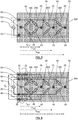
- the Figures 3 to 8 illustrate embodiments according to the present invention.
- the figure 3 presents a block diagram of a multi-bridge type arrangement, consisting of connecting to each other, according to a Wheatstone bridge, a plurality of detection branches 200 comprising at least one passive transducer 25 so that the plurality of branches detection 200 shares a common source of polarization 10 of a reference branch 100.
- the measurement signal V m for each measurand corresponds to the differential voltage between the midpoint of the so-called reference branch 100 (the impedances being sensitive or not to a measurand or to influence quantities) and the midpoint of a detection branch 200; said branch 200 being provided with at least one passive transducer 25, associated with a measurand.
- the invention proposes, among other things, to share a same reference branch 100 to generate the reference potential V o used by all the detection branches 200.
- the assembly requires only three branches to be polarized (ie a reference branch 100 and two detection branches 200) instead of four branches 100, 200 necessary in the assembly according to the prior art.
- the assembly according to the invention will require only eight branches to be polarized (ie a reference branch 100 and seven detection branches 200) instead of fourteen branches 100, 200 necessary in the assembly according to the prior art .
- the figure 4 illustrates the pooling of polarization pads 55 for sensors each having two advantageously passive transducers 25.
- figure 4 shows in particular the arrangement of the advantageously passive transducers 25 and a plurality of pads 50, 55.
- Two pads 55 among the plurality of pads 50, 55 are used to bias the detection branches 200 associated with each detection axis. These two pads 55 are advantageously connected to the polarization source 10.
- the measurement signal V m for each measurand is built on the potential difference between the midpoint of each detection branch 200 and the midpoint of the reference branch 100
- a central measurement pad 50 is thus positioned at the midpoint of each detection branch 200, in order to extract a measurand for each detection branch 200.
- the interconnection of the detection branches 200 is performed on the substrate 300.
- the number of pads 50, 55 necessary for interfacing the substrate 300 that is to say the electromechanical microsystem with an external device (for example, another substrate, power sources, etc.). is then equal to n + 2, where n is the number of measurand
- a significant gain can, in a particularly advantageous manner, be obtained in terms of the number of polarization pads 55 and central measurement pads 50, in particular when the number of measurands at the level of the substrate 300 preferably comprises an electromechanical microsystem (MEMS) becomes important.
- MEMS electromechanical microsystem
- the invention is not limited to electromechanical microsystems but also applies to electromechanical nanosystems (NEMS).
- the figure 5 illustrates an assembly according to the present invention in which the reference branch 100 is integrated in the substrate 300, that is to say to the electromechanical microsystem.
- the reference branch 100 is advantageously supplied by the same pads 55 as the detection branches 200.
- An additional central measurement pad 50 is necessary to reach the midpoint of the reference branch 100 which generates the reference potential.
- the number of pads 50, 55 required is thus equal, in this embodiment, to n + 3, where n is the number of measurands.
- the reference branch 100 makes it possible to reproduce the potential of the detection branches 200 associated with each measurand when the latter are at rest.
- the reference branch 100, integrated into the substrate 300 comprising an electromechanical microsystem is thus placed near the various sensors.
- This reference branch 100 can, according to a particularly advantageous embodiment, be connected to the rest of the assembly by means of electrical tracks present, for example, on the substrate 300, advantageously on the electromechanical microsystem.
- the reference branch 100 may advantageously be made with the same advantageously passive transducers 25 as the detection branches 200.
- the reference branch 100 will thus advantageously have a behavior similar to, or even identical to, the detection branches 200 vis-à-vis -volumes of influence.
- the tracks associated with the mid-bridge potentials of the detection branches 200 and the reference branch 100 can advantageously be kept close to one another. This arrangement promotes, among other things, a reduction in the sensitivity to electromagnetic disturbances that affect the differential mode of the measurement signals (for example, induction loops, capacitive coupling, inductive coupling, etc.).
- the potential of the bridge medium of the reference branch 100 will be modified in the same way as the potential V m of the branches of detection 200.
- the reference branch 100 is insensitive to one of the multisensory sensor measurands.
- a detection branch 200 can be sensitive to the combination of the acceleration and the magnetic field ⁇ xa + B, where a is a measurand, B the value of the magnetic field.
- the measurement signal V m makes it possible to obtain the value of the magnetic field B alone.
- the signal present on the reference branch 100 is subtracted from all the detection branches 200. This embodiment is particularly advantageous in the case where all the detection branches 200 are affected by the same. by the same measurand.
- the figure 6 illustrates an embodiment where two additional measurement pads 56 have been added in an assembly in order to control the bias voltage V p of the detection branches 200.
- These additional measurement pads 56 preferably positioned on the substrate 300, advantageously allow measuring the bridge voltage and thereby provide a correction to the measurement signal V m. The ratio between these two signals makes it possible to eliminate the influence of the extra-bridge dipoles.
- These additional access measurement pads 56 may comprise unstable or high-value dipoles (for example, resistors) such as those produced during eutectic sealing between two materials, for example between gold (Au ) and silicon (Si). Their impact is even more negligible as the input impedance of the voltage measurement stage is important.
- the different detection branches 200 present in the assembly can in certain situations have effects on one another.
- the dipoles 25 are not perfectly balanced within each detection branch 200 and / or do not have the same sensitivity, the overall impedance of all the detection branches 200 and reference can be modified. This effect can then be reflected in the overall impedance of the multi-bridge circuit in which the impedances of the detection branches 200 are connected in parallel. This has the effect of altering the bias voltage actually applied to terminals of the detection branches 200.
- the solution proposed makes it possible to respond to this problem. From an electrical point of view, the disturbance perceived by each detection branch 200 is identical to that in which extra-bridge dipoles modify the bias voltage of the multi-bridge circuit.
- the figure 7 is a schematic representation of the electrical circuit forming in part the measuring sensor according to the present invention.
- the reference branch 100 and the detection branches 200 are located on a first substrate 300, preferably forming an electromechanical microsystem.
- the pads 50, 55, 56 are positioned on the first substrate 300 and / or on the second substrate 350.
- the pads 50, 55, 56 are positioned only on a second substrate 350.
- the first and second substrates 300, 350 are made of a semiconductor material.
- the substrates 300, 350 may, for example, be formed based on silicon.
- the dipoles which connect the advantageously passive transducers 25 to the substrate 300 constitute intra-bridge parasitic dipoles 45.
- the intra-bridge parasitic dipoles 45 In order to reduce the problems of resistance, the intra-bridge parasitic dipoles 45 must be reduced as much as possible. have a negligible impact on the operation of the sensor if their value does not exceed 1% of the impedance of the advantageously passive transducers 25. This value is acceptable if, for example, the stability of these parasitic dipoles is found to be 1%.
- the overall disturbance provided to the detection branch 200 is of the order of 100 parts per million (ppm) of the value of the impedance of the transducer 25. This level of disturbance must be less than the minimum variation sought. for this same transducer 25.
- the extra-bridge parasitic dipoles 65, 75 are all outside the multi-bridge assembly.
- intra-bridge access dipoles 45 remain between the advantageously passive transducers 25, these can be integrated into the impedances of the transducers advantageously passive if their behavior vis-à-vis the influence quantities is identical.
- the bias voltage applied at the two interconnection nodes of the branches 100, 200 can be altered by these extra-bridge parasitic dipoles 65, 75.
- the manufacturing method can generate high interconnection parasitic dipoles 65.
- a metal seal for example of the eutectic type (gold-silicon (Au-Si), aluminum-germanium (Al-Ge) gold-tin (Au-Sn), etc.)
- Au-Si gold-silicon
- Al-Ge aluminum-germanium
- Au-Sn gold-tin
- the value of the parasitic dipole 65 of such a seal may be important.
- the parasitic dipoles 65 of the seal should preferably be arranged outside the Wheatstone bridges, for example at the interface between the first and a second substrate 350, different from the first substrate 300, comprising the bridges. of Wheatstone.
- this can be achieved by means of a continuous layer of electrically conductive materials.
- This layer may consist, for example, of doped silicon and a metal such as aluminum.
- the use of a good conductivity material makes it possible effectively to reduce the dipoles of the tracks between two transducers 25 by means of adequate sizing of the tracks.
- impedance tracks of less than 1 ohm can be manufactured with a layer of silicon and aluminum and be negligible compared to the advantageously passive transducers with impedances close to 2000 ohms.
- the proposed arrangement thus provides a solution to the problem in which contact dipoles of high value or unstable behavior may appear during the sealing of a first substrate 300 and a second substrate 350, at their pads 50, 55, 56. A discontinuity is thus obtained between the conductors of the first substrate 300 and the second substrate 350.
- the high-value parasitic dipoles 65 of the metal seal are positioned outside the bridges, and are excluded from the measuring circuit, if their dipole is weak in front of the input impedance of the voltage measuring stage V p and V m .
- a first substrate 300 preferably comprises an electromechanical microsystem formed by at least one electrical circuit, interconnect tracks 600 and gauges 700.
- the first substrate 300 advantageously comprises interconnection tracks 600 configured to convey the information (for example: for example, the physical quantities, the electrical signal) of a stud 50, 55, 56 to another.
- a second substrate 350 is advantageously sealed to the first substrate 300 by means of a sealing of interconnect tracks 600, so as to form a cavity accommodating at least the gauges 700.
- the gauges 700 are, according to a preferred embodiment, piezoresistive type. For example, with gauge sensors, an elastic deformation of the measuring element is first converted into a resistance variation of the gauge, to then generate an electrical output signal of a Wheatstone bridge circuit.
- the circuit comprises at least one mobile mass.
- the pads 50, 55, 56 are positioned on a second substrate 350.
- the figure 8 represents a sensor with two measurands.
- 5 pads 50, 55, 56 are positioned on the second substrate 350: two pads 55 for the polarization, one central measurement pad 50 for the reference branch 100 and two measurement pads 50 for the two measured quantities. from the two detection branches 200.
- the following table compares the number of pads 50, 55, 56 required on the substrate 300 in order to achieve various configurations.
- two advantageously passive transducers 25 are present on each detection branch 200.
- Each configuration proposed in the table makes it possible to remedy certain problems that may be encountered, in practice, when setting up a circuit board. measurement (for example, problems related to the unbalanced branches of the Wheatstone bridge, parasitic dipoles 45, 65, 75, etc.).
- the assembly allows a gain (or a reduction) in terms of the number of pads 50, 55, 56 for each situation, regardless of the number of measurands n, in particular for a number n greater than 1.
- the pooling of the polarization source 10 for all the detection branches 200 does not make it possible to control, measured by measurand, the polarization state of the advantageously passive transducers 25.
- the bias voltage can be activated intermittently at a high frequency (March 10-April 10 kHz), with a low duty cycle (e.g., less than 0.2).
- the first consists of n signal conditioning stages that can be integrated within the application-specific integrated circuit (in English, acronym “ASIC” for "Application-Specific Integrated Circuit"), in order to address each component simultaneously.
- ASIC Application-Specific Integrated Circuit
- this solution may require significant resources (for example, space occupied, energy consumption, etc.) for the reading electronics.
- the second method concerns the use of buffers (of the sample-and-hold type, for example) for each measurand, making it possible to conserve the voltage of mid-deck for subsequent conditioning.
- This solution then requires a single digital analog conversion stage, or even a single analog amplification stage.
- the present invention is not limited to the embodiments previously described but extends to any embodiment covered by the claims.
- the measurement circuit does not exclude the presence of other parts, including independent Wheatstone bridges in addition.
Landscapes
- Physics & Mathematics (AREA)
- General Physics & Mathematics (AREA)
- Condensed Matter Physics & Semiconductors (AREA)
- Pressure Sensors (AREA)
- Force Measurement Appropriate To Specific Purposes (AREA)
- Micromachines (AREA)
Claims (17)
- Messschaltung für einen multisensorischen Messwertaufnehmer, umfassend:- eine Vielzahl von Erfassungselementen (200), die parallel montiert sind, wobei jedes mindestens zwei in Serie montierte Dipole (25) umfasst,- und mindestens ein Referenzelement (100), umfassend eine Polarisationsquelle (10) und mindestens zwei in Serie montierte Dipole (25),dadurch gekennzeichnet, dass das Referenzelement (100) elektrisch parallel mit mindestens zwei Erfassungselementen (200) unter der Vielzahl von Elementen verbunden ist, um eine Wheatstone-Brücke mit jedem der Erfassungselemente (200) unter der Vielzahl von Erfassungselementen (200) zu bilden.
- Schaltung nach dem vorhergehenden Anspruch, umfassend mindestens einen Dipol (25) mit variabler Impedanz in Abhängigkeit von der Entwicklung einer Messgröße in mindestens einem Erfassungselement (200).
- Schaltung nach einem der vorhergehenden Ansprüche, bei der das Referenzelement (100) mit den Erfassungselementen (200) mit Hilfe eines ersten Polarisationsblocks und eines zweiten Polarisationsblocks (55) verbunden ist.
- Schaltung nach einem der vorhergehenden Ansprüche, bei der jedes Erfassungselement (200) mit mindestens einem zentralen Messblock (50), der sich zwischen den Dipolen (25) des Erfassungselements befindet, am Mittelpunkt der Erfassungselemente (200) verbunden ist.
- Schaltung nach einem der vorhergehenden Ansprüche, umfassend zwei zusätzliche Messblöcke (56), die parallel montiert und dazu vorgesehen sind, die Polarisationsspannung der Erfassungselemente (200) zu kontrollieren.
- Multisensorischer Messwertaufnehmer, umfassend mindestens eine Messschaltung nach einem der vorhergehenden Ansprüche.
- Messwertaufnehmer nach dem vorhergehenden Anspruch, bei dem die Messschaltung zumindest teilweise auf einem ersten Substrat (300) und einem zweiten Substrat (350) gebildet ist; wobei die Substrate (300, 350) zusammengefügt sind, um einen Hohlraum zu bilden.
- Messwertaufnehmer nach dem vorhergehenden Anspruch, umfassend eine Schaltung nach Anspruch 5, bei der das Referenzelement (100) parallel mit den Erfassungselementen (200) mit Hilfe des ersten Polarisationsblocks und des zweiten Polarisationsblocks (55) verbunden ist; wobei die zentralen (50) und zusätzlichen (56) Messblöcke sowie die Polarisationsblöcke (55) auf dem ersten und/oder auf dem zweiten Substrat (350) angeordnet sind.
- Messwertaufnehmer nach einem der vorhergehenden Ansprüche, bei dem das Referenzelement (100) zumindest teilweise auf dem ersten Substrat (300) positioniert ist.
- Messwertaufnehmer nach einem der drei vorhergehenden Ansprüche, bei dem das Referenzelement (100) zumindest teilweise auf dem zweiten Substrat (350) positioniert ist.
- Messwertaufnehmer nach einem der vier vorhergehenden Ansprüche, bei dem jedes Erfassungselement (200) zumindest teilweise auf dem ersten Substrat (300) positioniert ist.
- Messwertaufnehmer nach einem der fünf vorhergehenden Ansprüche, bei dem jedes Erfassungselement (200) mit mindestens einem zentralen Messblock (50) verbunden ist; wobei der zentrale Messblock (50) auf dem zweiten Substrat (350) oder auf dem ersten Substrat (300) angeordnet ist.
- Messwertaufnehmer nach einem der sechs vorhergehenden Ansprüche, umfassend ein elektromechanisches Mikrosystem und/oder Nanosystem.
- Messwertaufnehmer nach dem vorhergehenden Anspruch, bei dem das elektromechanische Mikrosystem und/oder Nanosystem in dem Hohlraum angeordnet ist.
- Messwertaufnehmer nach einem der zwei vorhergehenden Ansprüche, bei dem das elektronmechanische Mikrosystem und/oder Nanosystem mindestens eine mobile Masse umfasst.
- Messwertaufnehmer nach einem der drei vorhergehenden Ansprüche, bei dem das elektromechanische Mikrosystem und/oder Nanosystem auf dem ersten Substrat (300) hergestellt ist.
- Messwertaufnehmer nach einem der Ansprüche 6 bis 16, bei dem das erste Substrat (300) Verbindungsspuren (600) umfasst.
Applications Claiming Priority (1)
| Application Number | Priority Date | Filing Date | Title |
|---|---|---|---|
| FR1363189A FR3015688B1 (fr) | 2013-12-20 | 2013-12-20 | Capteur multi-sensoriel |
Publications (2)
| Publication Number | Publication Date |
|---|---|
| EP2887086A1 EP2887086A1 (de) | 2015-06-24 |
| EP2887086B1 true EP2887086B1 (de) | 2017-08-23 |
Family
ID=50624699
Family Applications (1)
| Application Number | Title | Priority Date | Filing Date |
|---|---|---|---|
| EP14198979.8A Active EP2887086B1 (de) | 2013-12-20 | 2014-12-18 | Multisensorischer messwertaufnehmer |
Country Status (4)
| Country | Link |
|---|---|
| US (1) | US10126333B2 (de) |
| EP (1) | EP2887086B1 (de) |
| CN (1) | CN104729580B (de) |
| FR (1) | FR3015688B1 (de) |
Families Citing this family (3)
| Publication number | Priority date | Publication date | Assignee | Title |
|---|---|---|---|---|
| US10704969B2 (en) * | 2017-11-21 | 2020-07-07 | The Boeing Company | Stress sensor |
| CN114858124B (zh) * | 2022-04-14 | 2023-04-07 | 广东省水利水电科学研究院 | 一种大坝表面变形监测系统及方法 |
| CN115166369B (zh) * | 2022-07-06 | 2025-06-13 | 厦门乃尔电子有限公司 | 一种两线制iepe传感器输出阻抗的测试方法 |
Family Cites Families (20)
| Publication number | Priority date | Publication date | Assignee | Title |
|---|---|---|---|---|
| US3784906A (en) * | 1971-11-01 | 1974-01-08 | Biddle Co J | Bridge having multiple nulls |
| US6701296B1 (en) * | 1988-10-14 | 2004-03-02 | James F. Kramer | Strain-sensing goniometers, systems, and recognition algorithms |
| US6422088B1 (en) * | 1999-09-24 | 2002-07-23 | Denso Corporation | Sensor failure or abnormality detecting system incorporated in a physical or dynamic quantity detecting apparatus |
| US7112951B2 (en) * | 2004-06-07 | 2006-09-26 | General Electric Company | MEMS based current sensor using magnetic-to-mechanical conversion and reference components |
| GB2418989A (en) * | 2004-10-06 | 2006-04-12 | Autoliv Dev | Vehicle deformation crash sensor |
| US7812416B2 (en) * | 2006-05-22 | 2010-10-12 | Cardiomems, Inc. | Methods and apparatus having an integrated circuit attached to fused silica |
| DE102006032277B4 (de) * | 2006-07-12 | 2017-06-01 | Infineon Technologies Ag | Magnetfeldsensorbauelement |
| KR20090045406A (ko) * | 2006-08-30 | 2009-05-07 | 알프스 덴키 가부시키가이샤 | 자기검출장치 |
| DE102007029817B9 (de) * | 2007-06-28 | 2017-01-12 | Infineon Technologies Ag | Magnetfeldsensor und Verfahren zur Kalibration eines Magnetfeldsensors |
| FR2924422B1 (fr) | 2007-11-30 | 2009-12-25 | Commissariat Energie Atomique | Dispositif a detection par jauge de contrainte piezoresistive suspendue comportant une cellule d'amplification de contrainte. |
| FR2942316B1 (fr) * | 2009-02-13 | 2011-07-22 | Commissariat Energie Atomique | Capteur de force de contact |
| FR2951826B1 (fr) | 2009-10-23 | 2012-06-15 | Commissariat Energie Atomique | Capteur a detection piezoresistive dans le plan |
| IT1402178B1 (it) * | 2010-09-09 | 2013-08-28 | St Microelectronics Srl | Circuito di lettura a compensazione automatica dell'offset per un sensore di campo magnetico e relativo metodo di lettura a compensazione automatica dell'offset |
| JP5419923B2 (ja) * | 2011-05-09 | 2014-02-19 | 三菱電機株式会社 | センサー素子 |
| US8878528B2 (en) * | 2011-06-30 | 2014-11-04 | Silicon Laboratories Inc. | MEMS-based magnetic sensor with a Lorentz force actuator used as force feedback |
| FR2977319B1 (fr) | 2011-07-01 | 2014-03-14 | Commissariat Energie Atomique | Dispositif de mesure de pression a sensiblite optimisee |
| US8466523B2 (en) * | 2011-10-07 | 2013-06-18 | Continental Automotive Systems, Inc. | Differential pressure sensor device |
| US9470710B2 (en) * | 2013-02-27 | 2016-10-18 | Texas Instruments Incorporated | Capacitive MEMS sensor devices |
| US9650237B2 (en) * | 2013-04-19 | 2017-05-16 | Agency For Science, Technology And Research | Electromechanical device including a suspended structure and method of fabricating the same |
| EP2806258B1 (de) * | 2013-05-20 | 2018-09-12 | ams international AG | Differenzdrucksensor |
-
2013
- 2013-12-20 FR FR1363189A patent/FR3015688B1/fr not_active Expired - Fee Related
-
2014
- 2014-12-18 EP EP14198979.8A patent/EP2887086B1/de active Active
- 2014-12-19 US US14/576,991 patent/US10126333B2/en active Active
- 2014-12-22 CN CN201410806546.6A patent/CN104729580B/zh active Active
Non-Patent Citations (1)
| Title |
|---|
| None * |
Also Published As
| Publication number | Publication date |
|---|---|
| US10126333B2 (en) | 2018-11-13 |
| FR3015688A1 (fr) | 2015-06-26 |
| US20150177281A1 (en) | 2015-06-25 |
| FR3015688B1 (fr) | 2016-01-08 |
| EP2887086A1 (de) | 2015-06-24 |
| CN104729580A (zh) | 2015-06-24 |
| CN104729580B (zh) | 2019-06-28 |
Similar Documents
| Publication | Publication Date | Title |
|---|---|---|
| CN102298075B (zh) | 一种具有复合多梁结构的加速度传感器芯片及其制作方法 | |
| US12203819B2 (en) | Temperature coefficient of offset compensation for force sensor and strain gauge | |
| EP2933224A1 (de) | Messkreis | |
| FR2957414A1 (fr) | Capteur de force a bruit reduit | |
| FR2672130A1 (fr) | Accelerometre miniature et procede pour capter une acceleration. | |
| EP2823273B1 (de) | Verfahren zur herstellung eines drucksensors | |
| FR3012604A1 (fr) | Capteur de pression comprenant une structure de controle d'une couche d'adhesif resistante aux variations de temperatures | |
| FR2969278A1 (fr) | Structure planaire pour gyrometre tri-axe | |
| WO2010092092A1 (fr) | Capteur de force de contact | |
| EP1835263B1 (de) | Elektronischer Schnittstellenschaltkreis eines kapazitiven Sensors zur Messung eines physikalischen Parameters und Verfahren zur Ingangsetzung des elektronischen Schaltkreises | |
| EP2887086A1 (de) | Multisensorischer Messwertaufnehmer | |
| FR2865275A1 (fr) | Element d'acquisition de grandeur physique ayant une structure amelioree convenant pour une liaison electrique et son procede de fabrication | |
| WO2014049062A1 (fr) | Capteur de pression a base de nanojauges couplees a un resonateur | |
| EP1963779B1 (de) | Vorrichtung zur aufnahme einer lagerung mit einem system zur erkennung der auf die lagerung gelegten last. | |
| WO2024213465A1 (fr) | Dispositif piezoelectrique flexible de mesure de deformation, unidirectionnel, bidirectionel ou omnidirectionnel | |
| CN1866031A (zh) | 超小型加速度计 | |
| EP1353185B1 (de) | Ineritalsensor mit integrierter Temperatursonde | |
| FR3112392A1 (fr) | Accéléromètre industriel triaxial | |
| WO2018178564A1 (fr) | Capteur pour mesurer des forces d'accélération selon trois axes | |
| WO2018219683A1 (fr) | Capteur de déformation monobloc et procédé de mesure de la déformation d'une surface d'un solide | |
| JP2008216135A (ja) | 容量式物理量検出装置 | |
| EP1963808B1 (de) | Vorrichtung zur lastenmessung | |
| FR3067459A1 (fr) | Capteur numerique de pression | |
| FR3031639A1 (fr) | Transducteur electromecanique integrant un element deformable de type resonateur ou membrane, et capteur de mesure integrant un tel transducteur | |
| FR3023279A1 (fr) | Module sensible et centrale de mesure |
Legal Events
| Date | Code | Title | Description |
|---|---|---|---|
| PUAI | Public reference made under article 153(3) epc to a published international application that has entered the european phase |
Free format text: ORIGINAL CODE: 0009012 |
|
| 17P | Request for examination filed |
Effective date: 20141218 |
|
| AK | Designated contracting states |
Kind code of ref document: A1 Designated state(s): AL AT BE BG CH CY CZ DE DK EE ES FI FR GB GR HR HU IE IS IT LI LT LU LV MC MK MT NL NO PL PT RO RS SE SI SK SM TR |
|
| AX | Request for extension of the european patent |
Extension state: BA ME |
|
| R17P | Request for examination filed (corrected) |
Effective date: 20151210 |
|
| RBV | Designated contracting states (corrected) |
Designated state(s): AL AT BE BG CH CY CZ DE DK EE ES FI FR GB GR HR HU IE IS IT LI LT LU LV MC MK MT NL NO PL PT RO RS SE SI SK SM TR |
|
| RIC1 | Information provided on ipc code assigned before grant |
Ipc: G01R 33/038 20060101ALI20170214BHEP Ipc: G01R 33/02 20060101AFI20170214BHEP |
|
| GRAP | Despatch of communication of intention to grant a patent |
Free format text: ORIGINAL CODE: EPIDOSNIGR1 |
|
| STAA | Information on the status of an ep patent application or granted ep patent |
Free format text: STATUS: GRANT OF PATENT IS INTENDED |
|
| INTG | Intention to grant announced |
Effective date: 20170406 |
|
| RIN1 | Information on inventor provided before grant (corrected) |
Inventor name: JOURDAN, GUILLAUME Inventor name: REY, PATRICE Inventor name: ROBERT, PHILIPPE Inventor name: DIEM, BERNARD |
|
| GRAS | Grant fee paid |
Free format text: ORIGINAL CODE: EPIDOSNIGR3 |
|
| GRAA | (expected) grant |
Free format text: ORIGINAL CODE: 0009210 |
|
| STAA | Information on the status of an ep patent application or granted ep patent |
Free format text: STATUS: THE PATENT HAS BEEN GRANTED |
|
| AK | Designated contracting states |
Kind code of ref document: B1 Designated state(s): AL AT BE BG CH CY CZ DE DK EE ES FI FR GB GR HR HU IE IS IT LI LT LU LV MC MK MT NL NO PL PT RO RS SE SI SK SM TR |
|
| REG | Reference to a national code |
Ref country code: GB Ref legal event code: FG4D Free format text: NOT ENGLISH |
|
| REG | Reference to a national code |
Ref country code: CH Ref legal event code: EP |
|
| REG | Reference to a national code |
Ref country code: AT Ref legal event code: REF Ref document number: 921920 Country of ref document: AT Kind code of ref document: T Effective date: 20170915 |
|
| REG | Reference to a national code |
Ref country code: IE Ref legal event code: FG4D Free format text: LANGUAGE OF EP DOCUMENT: FRENCH |
|
| REG | Reference to a national code |
Ref country code: DE Ref legal event code: R096 Ref document number: 602014013437 Country of ref document: DE |
|
| REG | Reference to a national code |
Ref country code: FR Ref legal event code: PLFP Year of fee payment: 4 |
|
| REG | Reference to a national code |
Ref country code: NL Ref legal event code: MP Effective date: 20170823 |
|
| REG | Reference to a national code |
Ref country code: LT Ref legal event code: MG4D |
|
| REG | Reference to a national code |
Ref country code: AT Ref legal event code: MK05 Ref document number: 921920 Country of ref document: AT Kind code of ref document: T Effective date: 20170823 |
|
| PG25 | Lapsed in a contracting state [announced via postgrant information from national office to epo] |
Ref country code: NL Free format text: LAPSE BECAUSE OF FAILURE TO SUBMIT A TRANSLATION OF THE DESCRIPTION OR TO PAY THE FEE WITHIN THE PRESCRIBED TIME-LIMIT Effective date: 20170823 Ref country code: NO Free format text: LAPSE BECAUSE OF FAILURE TO SUBMIT A TRANSLATION OF THE DESCRIPTION OR TO PAY THE FEE WITHIN THE PRESCRIBED TIME-LIMIT Effective date: 20171123 Ref country code: HR Free format text: LAPSE BECAUSE OF FAILURE TO SUBMIT A TRANSLATION OF THE DESCRIPTION OR TO PAY THE FEE WITHIN THE PRESCRIBED TIME-LIMIT Effective date: 20170823 Ref country code: FI Free format text: LAPSE BECAUSE OF FAILURE TO SUBMIT A TRANSLATION OF THE DESCRIPTION OR TO PAY THE FEE WITHIN THE PRESCRIBED TIME-LIMIT Effective date: 20170823 Ref country code: LT Free format text: LAPSE BECAUSE OF FAILURE TO SUBMIT A TRANSLATION OF THE DESCRIPTION OR TO PAY THE FEE WITHIN THE PRESCRIBED TIME-LIMIT Effective date: 20170823 Ref country code: SE Free format text: LAPSE BECAUSE OF FAILURE TO SUBMIT A TRANSLATION OF THE DESCRIPTION OR TO PAY THE FEE WITHIN THE PRESCRIBED TIME-LIMIT Effective date: 20170823 Ref country code: AT Free format text: LAPSE BECAUSE OF FAILURE TO SUBMIT A TRANSLATION OF THE DESCRIPTION OR TO PAY THE FEE WITHIN THE PRESCRIBED TIME-LIMIT Effective date: 20170823 |
|
| PG25 | Lapsed in a contracting state [announced via postgrant information from national office to epo] |
Ref country code: RS Free format text: LAPSE BECAUSE OF FAILURE TO SUBMIT A TRANSLATION OF THE DESCRIPTION OR TO PAY THE FEE WITHIN THE PRESCRIBED TIME-LIMIT Effective date: 20170823 Ref country code: BG Free format text: LAPSE BECAUSE OF FAILURE TO SUBMIT A TRANSLATION OF THE DESCRIPTION OR TO PAY THE FEE WITHIN THE PRESCRIBED TIME-LIMIT Effective date: 20171123 Ref country code: LV Free format text: LAPSE BECAUSE OF FAILURE TO SUBMIT A TRANSLATION OF THE DESCRIPTION OR TO PAY THE FEE WITHIN THE PRESCRIBED TIME-LIMIT Effective date: 20170823 Ref country code: ES Free format text: LAPSE BECAUSE OF FAILURE TO SUBMIT A TRANSLATION OF THE DESCRIPTION OR TO PAY THE FEE WITHIN THE PRESCRIBED TIME-LIMIT Effective date: 20170823 Ref country code: IS Free format text: LAPSE BECAUSE OF FAILURE TO SUBMIT A TRANSLATION OF THE DESCRIPTION OR TO PAY THE FEE WITHIN THE PRESCRIBED TIME-LIMIT Effective date: 20171223 Ref country code: GR Free format text: LAPSE BECAUSE OF FAILURE TO SUBMIT A TRANSLATION OF THE DESCRIPTION OR TO PAY THE FEE WITHIN THE PRESCRIBED TIME-LIMIT Effective date: 20171124 Ref country code: PL Free format text: LAPSE BECAUSE OF FAILURE TO SUBMIT A TRANSLATION OF THE DESCRIPTION OR TO PAY THE FEE WITHIN THE PRESCRIBED TIME-LIMIT Effective date: 20170823 |
|
| PG25 | Lapsed in a contracting state [announced via postgrant information from national office to epo] |
Ref country code: RO Free format text: LAPSE BECAUSE OF FAILURE TO SUBMIT A TRANSLATION OF THE DESCRIPTION OR TO PAY THE FEE WITHIN THE PRESCRIBED TIME-LIMIT Effective date: 20170823 Ref country code: CZ Free format text: LAPSE BECAUSE OF FAILURE TO SUBMIT A TRANSLATION OF THE DESCRIPTION OR TO PAY THE FEE WITHIN THE PRESCRIBED TIME-LIMIT Effective date: 20170823 Ref country code: DK Free format text: LAPSE BECAUSE OF FAILURE TO SUBMIT A TRANSLATION OF THE DESCRIPTION OR TO PAY THE FEE WITHIN THE PRESCRIBED TIME-LIMIT Effective date: 20170823 |
|
| REG | Reference to a national code |
Ref country code: DE Ref legal event code: R097 Ref document number: 602014013437 Country of ref document: DE |
|
| PG25 | Lapsed in a contracting state [announced via postgrant information from national office to epo] |
Ref country code: SK Free format text: LAPSE BECAUSE OF FAILURE TO SUBMIT A TRANSLATION OF THE DESCRIPTION OR TO PAY THE FEE WITHIN THE PRESCRIBED TIME-LIMIT Effective date: 20170823 Ref country code: IT Free format text: LAPSE BECAUSE OF FAILURE TO SUBMIT A TRANSLATION OF THE DESCRIPTION OR TO PAY THE FEE WITHIN THE PRESCRIBED TIME-LIMIT Effective date: 20170823 Ref country code: EE Free format text: LAPSE BECAUSE OF FAILURE TO SUBMIT A TRANSLATION OF THE DESCRIPTION OR TO PAY THE FEE WITHIN THE PRESCRIBED TIME-LIMIT Effective date: 20170823 Ref country code: SM Free format text: LAPSE BECAUSE OF FAILURE TO SUBMIT A TRANSLATION OF THE DESCRIPTION OR TO PAY THE FEE WITHIN THE PRESCRIBED TIME-LIMIT Effective date: 20170823 |
|
| PLBE | No opposition filed within time limit |
Free format text: ORIGINAL CODE: 0009261 |
|
| STAA | Information on the status of an ep patent application or granted ep patent |
Free format text: STATUS: NO OPPOSITION FILED WITHIN TIME LIMIT |
|
| REG | Reference to a national code |
Ref country code: CH Ref legal event code: PL |
|
| 26N | No opposition filed |
Effective date: 20180524 |
|
| PG25 | Lapsed in a contracting state [announced via postgrant information from national office to epo] |
Ref country code: SI Free format text: LAPSE BECAUSE OF FAILURE TO SUBMIT A TRANSLATION OF THE DESCRIPTION OR TO PAY THE FEE WITHIN THE PRESCRIBED TIME-LIMIT Effective date: 20170823 |
|
| REG | Reference to a national code |
Ref country code: IE Ref legal event code: MM4A |
|
| PG25 | Lapsed in a contracting state [announced via postgrant information from national office to epo] |
Ref country code: MT Free format text: LAPSE BECAUSE OF FAILURE TO SUBMIT A TRANSLATION OF THE DESCRIPTION OR TO PAY THE FEE WITHIN THE PRESCRIBED TIME-LIMIT Effective date: 20170823 Ref country code: LU Free format text: LAPSE BECAUSE OF NON-PAYMENT OF DUE FEES Effective date: 20171218 |
|
| REG | Reference to a national code |
Ref country code: BE Ref legal event code: MM Effective date: 20171231 |
|
| PG25 | Lapsed in a contracting state [announced via postgrant information from national office to epo] |
Ref country code: IE Free format text: LAPSE BECAUSE OF NON-PAYMENT OF DUE FEES Effective date: 20171218 |
|
| PG25 | Lapsed in a contracting state [announced via postgrant information from national office to epo] |
Ref country code: LI Free format text: LAPSE BECAUSE OF NON-PAYMENT OF DUE FEES Effective date: 20171231 Ref country code: CH Free format text: LAPSE BECAUSE OF NON-PAYMENT OF DUE FEES Effective date: 20171231 Ref country code: BE Free format text: LAPSE BECAUSE OF NON-PAYMENT OF DUE FEES Effective date: 20171231 |
|
| PG25 | Lapsed in a contracting state [announced via postgrant information from national office to epo] |
Ref country code: HU Free format text: LAPSE BECAUSE OF FAILURE TO SUBMIT A TRANSLATION OF THE DESCRIPTION OR TO PAY THE FEE WITHIN THE PRESCRIBED TIME-LIMIT; INVALID AB INITIO Effective date: 20141218 Ref country code: MC Free format text: LAPSE BECAUSE OF FAILURE TO SUBMIT A TRANSLATION OF THE DESCRIPTION OR TO PAY THE FEE WITHIN THE PRESCRIBED TIME-LIMIT Effective date: 20170823 |
|
| PG25 | Lapsed in a contracting state [announced via postgrant information from national office to epo] |
Ref country code: CY Free format text: LAPSE BECAUSE OF FAILURE TO SUBMIT A TRANSLATION OF THE DESCRIPTION OR TO PAY THE FEE WITHIN THE PRESCRIBED TIME-LIMIT Effective date: 20170823 |
|
| PG25 | Lapsed in a contracting state [announced via postgrant information from national office to epo] |
Ref country code: MK Free format text: LAPSE BECAUSE OF FAILURE TO SUBMIT A TRANSLATION OF THE DESCRIPTION OR TO PAY THE FEE WITHIN THE PRESCRIBED TIME-LIMIT Effective date: 20170823 |
|
| PG25 | Lapsed in a contracting state [announced via postgrant information from national office to epo] |
Ref country code: TR Free format text: LAPSE BECAUSE OF FAILURE TO SUBMIT A TRANSLATION OF THE DESCRIPTION OR TO PAY THE FEE WITHIN THE PRESCRIBED TIME-LIMIT Effective date: 20170823 |
|
| PG25 | Lapsed in a contracting state [announced via postgrant information from national office to epo] |
Ref country code: PT Free format text: LAPSE BECAUSE OF FAILURE TO SUBMIT A TRANSLATION OF THE DESCRIPTION OR TO PAY THE FEE WITHIN THE PRESCRIBED TIME-LIMIT Effective date: 20170823 |
|
| PG25 | Lapsed in a contracting state [announced via postgrant information from national office to epo] |
Ref country code: AL Free format text: LAPSE BECAUSE OF FAILURE TO SUBMIT A TRANSLATION OF THE DESCRIPTION OR TO PAY THE FEE WITHIN THE PRESCRIBED TIME-LIMIT Effective date: 20170823 |
|
| PGFP | Annual fee paid to national office [announced via postgrant information from national office to epo] |
Ref country code: GB Payment date: 20251229 Year of fee payment: 12 |
|
| PGFP | Annual fee paid to national office [announced via postgrant information from national office to epo] |
Ref country code: FR Payment date: 20251222 Year of fee payment: 12 |
|
| PGFP | Annual fee paid to national office [announced via postgrant information from national office to epo] |
Ref country code: DE Payment date: 20251222 Year of fee payment: 12 |