EP2884332B1 - Display apparatus and illuminating apparatus - Google Patents
Display apparatus and illuminating apparatus Download PDFInfo
- Publication number
- EP2884332B1 EP2884332B1 EP13828432.8A EP13828432A EP2884332B1 EP 2884332 B1 EP2884332 B1 EP 2884332B1 EP 13828432 A EP13828432 A EP 13828432A EP 2884332 B1 EP2884332 B1 EP 2884332B1
- Authority
- EP
- European Patent Office
- Prior art keywords
- light
- electrode
- case
- linear
- dot
- Prior art date
- Legal status (The legal status is an assumption and is not a legal conclusion. Google has not performed a legal analysis and makes no representation as to the accuracy of the status listed.)
- Not-in-force
Links
Images


Classifications
-
- G—PHYSICS
- G02—OPTICS
- G02B—OPTICAL ELEMENTS, SYSTEMS OR APPARATUS
- G02B30/00—Optical systems or apparatus for producing three-dimensional [3D] effects, e.g. stereoscopic images
- G02B30/20—Optical systems or apparatus for producing three-dimensional [3D] effects, e.g. stereoscopic images by providing first and second parallax images to an observer's left and right eyes
- G02B30/26—Optical systems or apparatus for producing three-dimensional [3D] effects, e.g. stereoscopic images by providing first and second parallax images to an observer's left and right eyes of the autostereoscopic type
- G02B30/27—Optical systems or apparatus for producing three-dimensional [3D] effects, e.g. stereoscopic images by providing first and second parallax images to an observer's left and right eyes of the autostereoscopic type involving lenticular arrays
-
- G—PHYSICS
- G02—OPTICS
- G02F—OPTICAL DEVICES OR ARRANGEMENTS FOR THE CONTROL OF LIGHT BY MODIFICATION OF THE OPTICAL PROPERTIES OF THE MEDIA OF THE ELEMENTS INVOLVED THEREIN; NON-LINEAR OPTICS; FREQUENCY-CHANGING OF LIGHT; OPTICAL LOGIC ELEMENTS; OPTICAL ANALOGUE/DIGITAL CONVERTERS
- G02F1/00—Devices or arrangements for the control of the intensity, colour, phase, polarisation or direction of light arriving from an independent light source, e.g. switching, gating or modulating; Non-linear optics
- G02F1/01—Devices or arrangements for the control of the intensity, colour, phase, polarisation or direction of light arriving from an independent light source, e.g. switching, gating or modulating; Non-linear optics for the control of the intensity, phase, polarisation or colour
- G02F1/13—Devices or arrangements for the control of the intensity, colour, phase, polarisation or direction of light arriving from an independent light source, e.g. switching, gating or modulating; Non-linear optics for the control of the intensity, phase, polarisation or colour based on liquid crystals, e.g. single liquid crystal display cells
- G02F1/133—Constructional arrangements; Operation of liquid crystal cells; Circuit arrangements
- G02F1/1333—Constructional arrangements; Manufacturing methods
- G02F1/1335—Structural association of cells with optical devices, e.g. polarisers or reflectors
- G02F1/133526—Lenses, e.g. microlenses or Fresnel lenses
-
- G—PHYSICS
- G02—OPTICS
- G02B—OPTICAL ELEMENTS, SYSTEMS OR APPARATUS
- G02B3/00—Simple or compound lenses
- G02B3/0006—Arrays
- G02B3/0037—Arrays characterized by the distribution or form of lenses
- G02B3/0043—Inhomogeneous or irregular arrays, e.g. varying shape, size, height
-
- G—PHYSICS
- G02—OPTICS
- G02B—OPTICAL ELEMENTS, SYSTEMS OR APPARATUS
- G02B3/00—Simple or compound lenses
- G02B3/0006—Arrays
- G02B3/0037—Arrays characterized by the distribution or form of lenses
- G02B3/005—Arrays characterized by the distribution or form of lenses arranged along a single direction only, e.g. lenticular sheets
-
- G—PHYSICS
- G02—OPTICS
- G02B—OPTICAL ELEMENTS, SYSTEMS OR APPARATUS
- G02B30/00—Optical systems or apparatus for producing three-dimensional [3D] effects, e.g. stereoscopic images
- G02B30/20—Optical systems or apparatus for producing three-dimensional [3D] effects, e.g. stereoscopic images by providing first and second parallax images to an observer's left and right eyes
- G02B30/26—Optical systems or apparatus for producing three-dimensional [3D] effects, e.g. stereoscopic images by providing first and second parallax images to an observer's left and right eyes of the autostereoscopic type
- G02B30/30—Optical systems or apparatus for producing three-dimensional [3D] effects, e.g. stereoscopic images by providing first and second parallax images to an observer's left and right eyes of the autostereoscopic type involving parallax barriers
-
- G—PHYSICS
- G02—OPTICS
- G02F—OPTICAL DEVICES OR ARRANGEMENTS FOR THE CONTROL OF LIGHT BY MODIFICATION OF THE OPTICAL PROPERTIES OF THE MEDIA OF THE ELEMENTS INVOLVED THEREIN; NON-LINEAR OPTICS; FREQUENCY-CHANGING OF LIGHT; OPTICAL LOGIC ELEMENTS; OPTICAL ANALOGUE/DIGITAL CONVERTERS
- G02F1/00—Devices or arrangements for the control of the intensity, colour, phase, polarisation or direction of light arriving from an independent light source, e.g. switching, gating or modulating; Non-linear optics
- G02F1/01—Devices or arrangements for the control of the intensity, colour, phase, polarisation or direction of light arriving from an independent light source, e.g. switching, gating or modulating; Non-linear optics for the control of the intensity, phase, polarisation or colour
- G02F1/13—Devices or arrangements for the control of the intensity, colour, phase, polarisation or direction of light arriving from an independent light source, e.g. switching, gating or modulating; Non-linear optics for the control of the intensity, phase, polarisation or colour based on liquid crystals, e.g. single liquid crystal display cells
- G02F1/133—Constructional arrangements; Operation of liquid crystal cells; Circuit arrangements
- G02F1/1333—Constructional arrangements; Manufacturing methods
- G02F1/1335—Structural association of cells with optical devices, e.g. polarisers or reflectors
- G02F1/133504—Diffusing, scattering, diffracting elements
-
- G—PHYSICS
- G02—OPTICS
- G02F—OPTICAL DEVICES OR ARRANGEMENTS FOR THE CONTROL OF LIGHT BY MODIFICATION OF THE OPTICAL PROPERTIES OF THE MEDIA OF THE ELEMENTS INVOLVED THEREIN; NON-LINEAR OPTICS; FREQUENCY-CHANGING OF LIGHT; OPTICAL LOGIC ELEMENTS; OPTICAL ANALOGUE/DIGITAL CONVERTERS
- G02F1/00—Devices or arrangements for the control of the intensity, colour, phase, polarisation or direction of light arriving from an independent light source, e.g. switching, gating or modulating; Non-linear optics
- G02F1/01—Devices or arrangements for the control of the intensity, colour, phase, polarisation or direction of light arriving from an independent light source, e.g. switching, gating or modulating; Non-linear optics for the control of the intensity, phase, polarisation or colour
- G02F1/13—Devices or arrangements for the control of the intensity, colour, phase, polarisation or direction of light arriving from an independent light source, e.g. switching, gating or modulating; Non-linear optics for the control of the intensity, phase, polarisation or colour based on liquid crystals, e.g. single liquid crystal display cells
- G02F1/133—Constructional arrangements; Operation of liquid crystal cells; Circuit arrangements
- G02F1/1333—Constructional arrangements; Manufacturing methods
- G02F1/1335—Structural association of cells with optical devices, e.g. polarisers or reflectors
- G02F1/133528—Polarisers
-
- G—PHYSICS
- G02—OPTICS
- G02F—OPTICAL DEVICES OR ARRANGEMENTS FOR THE CONTROL OF LIGHT BY MODIFICATION OF THE OPTICAL PROPERTIES OF THE MEDIA OF THE ELEMENTS INVOLVED THEREIN; NON-LINEAR OPTICS; FREQUENCY-CHANGING OF LIGHT; OPTICAL LOGIC ELEMENTS; OPTICAL ANALOGUE/DIGITAL CONVERTERS
- G02F1/00—Devices or arrangements for the control of the intensity, colour, phase, polarisation or direction of light arriving from an independent light source, e.g. switching, gating or modulating; Non-linear optics
- G02F1/01—Devices or arrangements for the control of the intensity, colour, phase, polarisation or direction of light arriving from an independent light source, e.g. switching, gating or modulating; Non-linear optics for the control of the intensity, phase, polarisation or colour
- G02F1/13—Devices or arrangements for the control of the intensity, colour, phase, polarisation or direction of light arriving from an independent light source, e.g. switching, gating or modulating; Non-linear optics for the control of the intensity, phase, polarisation or colour based on liquid crystals, e.g. single liquid crystal display cells
- G02F1/133—Constructional arrangements; Operation of liquid crystal cells; Circuit arrangements
- G02F1/1333—Constructional arrangements; Manufacturing methods
- G02F1/1347—Arrangement of liquid crystal layers or cells in which the final condition of one light beam is achieved by the addition of the effects of two or more layers or cells
- G02F1/13476—Arrangement of liquid crystal layers or cells in which the final condition of one light beam is achieved by the addition of the effects of two or more layers or cells in which at least one liquid crystal cell or layer assumes a scattering state
-
- G—PHYSICS
- G09—EDUCATION; CRYPTOGRAPHY; DISPLAY; ADVERTISING; SEALS
- G09G—ARRANGEMENTS OR CIRCUITS FOR CONTROL OF INDICATING DEVICES USING STATIC MEANS TO PRESENT VARIABLE INFORMATION
- G09G3/00—Control arrangements or circuits, of interest only in connection with visual indicators other than cathode-ray tubes
- G09G3/001—Control arrangements or circuits, of interest only in connection with visual indicators other than cathode-ray tubes using specific devices not provided for in groups G09G3/02 - G09G3/36, e.g. using an intermediate record carrier such as a film slide; Projection systems; Display of non-alphanumerical information, solely or in combination with alphanumerical information, e.g. digital display on projected diapositive as background
- G09G3/003—Control arrangements or circuits, of interest only in connection with visual indicators other than cathode-ray tubes using specific devices not provided for in groups G09G3/02 - G09G3/36, e.g. using an intermediate record carrier such as a film slide; Projection systems; Display of non-alphanumerical information, solely or in combination with alphanumerical information, e.g. digital display on projected diapositive as background to produce spatial visual effects
-
- G—PHYSICS
- G09—EDUCATION; CRYPTOGRAPHY; DISPLAY; ADVERTISING; SEALS
- G09G—ARRANGEMENTS OR CIRCUITS FOR CONTROL OF INDICATING DEVICES USING STATIC MEANS TO PRESENT VARIABLE INFORMATION
- G09G3/00—Control arrangements or circuits, of interest only in connection with visual indicators other than cathode-ray tubes
- G09G3/20—Control arrangements or circuits, of interest only in connection with visual indicators other than cathode-ray tubes for presentation of an assembly of a number of characters, e.g. a page, by composing the assembly by combination of individual elements arranged in a matrix no fixed position being assigned to or needed to be assigned to the individual characters or partial characters
- G09G3/34—Control arrangements or circuits, of interest only in connection with visual indicators other than cathode-ray tubes for presentation of an assembly of a number of characters, e.g. a page, by composing the assembly by combination of individual elements arranged in a matrix no fixed position being assigned to or needed to be assigned to the individual characters or partial characters by control of light from an independent source
- G09G3/3406—Control of illumination source
-
- G—PHYSICS
- G09—EDUCATION; CRYPTOGRAPHY; DISPLAY; ADVERTISING; SEALS
- G09G—ARRANGEMENTS OR CIRCUITS FOR CONTROL OF INDICATING DEVICES USING STATIC MEANS TO PRESENT VARIABLE INFORMATION
- G09G3/00—Control arrangements or circuits, of interest only in connection with visual indicators other than cathode-ray tubes
- G09G3/20—Control arrangements or circuits, of interest only in connection with visual indicators other than cathode-ray tubes for presentation of an assembly of a number of characters, e.g. a page, by composing the assembly by combination of individual elements arranged in a matrix no fixed position being assigned to or needed to be assigned to the individual characters or partial characters
- G09G3/34—Control arrangements or circuits, of interest only in connection with visual indicators other than cathode-ray tubes for presentation of an assembly of a number of characters, e.g. a page, by composing the assembly by combination of individual elements arranged in a matrix no fixed position being assigned to or needed to be assigned to the individual characters or partial characters by control of light from an independent source
- G09G3/36—Control arrangements or circuits, of interest only in connection with visual indicators other than cathode-ray tubes for presentation of an assembly of a number of characters, e.g. a page, by composing the assembly by combination of individual elements arranged in a matrix no fixed position being assigned to or needed to be assigned to the individual characters or partial characters by control of light from an independent source using liquid crystals
-
- H—ELECTRICITY
- H04—ELECTRIC COMMUNICATION TECHNIQUE
- H04N—PICTORIAL COMMUNICATION, e.g. TELEVISION
- H04N13/00—Stereoscopic video systems; Multi-view video systems; Details thereof
- H04N13/30—Image reproducers
- H04N13/302—Image reproducers for viewing without the aid of special glasses, i.e. using autostereoscopic displays
- H04N13/305—Image reproducers for viewing without the aid of special glasses, i.e. using autostereoscopic displays using lenticular lenses, e.g. arrangements of cylindrical lenses
-
- H—ELECTRICITY
- H04—ELECTRIC COMMUNICATION TECHNIQUE
- H04N—PICTORIAL COMMUNICATION, e.g. TELEVISION
- H04N13/00—Stereoscopic video systems; Multi-view video systems; Details thereof
- H04N13/30—Image reproducers
- H04N13/302—Image reproducers for viewing without the aid of special glasses, i.e. using autostereoscopic displays
- H04N13/307—Image reproducers for viewing without the aid of special glasses, i.e. using autostereoscopic displays using fly-eye lenses, e.g. arrangements of circular lenses
-
- H—ELECTRICITY
- H04—ELECTRIC COMMUNICATION TECHNIQUE
- H04N—PICTORIAL COMMUNICATION, e.g. TELEVISION
- H04N13/00—Stereoscopic video systems; Multi-view video systems; Details thereof
- H04N13/30—Image reproducers
- H04N13/302—Image reproducers for viewing without the aid of special glasses, i.e. using autostereoscopic displays
- H04N13/31—Image reproducers for viewing without the aid of special glasses, i.e. using autostereoscopic displays using parallax barriers
- H04N13/312—Image reproducers for viewing without the aid of special glasses, i.e. using autostereoscopic displays using parallax barriers the parallax barriers being placed behind the display panel, e.g. between backlight and spatial light modulator [SLM]
-
- H—ELECTRICITY
- H04—ELECTRIC COMMUNICATION TECHNIQUE
- H04N—PICTORIAL COMMUNICATION, e.g. TELEVISION
- H04N13/00—Stereoscopic video systems; Multi-view video systems; Details thereof
- H04N13/30—Image reproducers
- H04N13/302—Image reproducers for viewing without the aid of special glasses, i.e. using autostereoscopic displays
- H04N13/317—Image reproducers for viewing without the aid of special glasses, i.e. using autostereoscopic displays using slanted parallax optics
-
- H—ELECTRICITY
- H04—ELECTRIC COMMUNICATION TECHNIQUE
- H04N—PICTORIAL COMMUNICATION, e.g. TELEVISION
- H04N13/00—Stereoscopic video systems; Multi-view video systems; Details thereof
- H04N13/30—Image reproducers
- H04N13/356—Image reproducers having separate monoscopic and stereoscopic modes
- H04N13/359—Switching between monoscopic and stereoscopic modes
-
- G—PHYSICS
- G02—OPTICS
- G02B—OPTICAL ELEMENTS, SYSTEMS OR APPARATUS
- G02B6/00—Light guides; Structural details of arrangements comprising light guides and other optical elements, e.g. couplings
- G02B6/0001—Light guides; Structural details of arrangements comprising light guides and other optical elements, e.g. couplings specially adapted for lighting devices or systems
- G02B6/0011—Light guides; Structural details of arrangements comprising light guides and other optical elements, e.g. couplings specially adapted for lighting devices or systems the light guides being planar or of plate-like form
- G02B6/0033—Means for improving the coupling-out of light from the light guide
- G02B6/0035—Means for improving the coupling-out of light from the light guide provided on the surface of the light guide or in the bulk of it
- G02B6/0038—Linear indentations or grooves, e.g. arc-shaped grooves or meandering grooves, extending over the full length or width of the light guide
-
- G—PHYSICS
- G02—OPTICS
- G02B—OPTICAL ELEMENTS, SYSTEMS OR APPARATUS
- G02B6/00—Light guides; Structural details of arrangements comprising light guides and other optical elements, e.g. couplings
- G02B6/0001—Light guides; Structural details of arrangements comprising light guides and other optical elements, e.g. couplings specially adapted for lighting devices or systems
- G02B6/0011—Light guides; Structural details of arrangements comprising light guides and other optical elements, e.g. couplings specially adapted for lighting devices or systems the light guides being planar or of plate-like form
- G02B6/0033—Means for improving the coupling-out of light from the light guide
- G02B6/0035—Means for improving the coupling-out of light from the light guide provided on the surface of the light guide or in the bulk of it
- G02B6/0045—Means for improving the coupling-out of light from the light guide provided on the surface of the light guide or in the bulk of it by shaping at least a portion of the light guide
- G02B6/0046—Tapered light guide, e.g. wedge-shaped light guide
-
- G—PHYSICS
- G02—OPTICS
- G02B—OPTICAL ELEMENTS, SYSTEMS OR APPARATUS
- G02B6/00—Light guides; Structural details of arrangements comprising light guides and other optical elements, e.g. couplings
- G02B6/0001—Light guides; Structural details of arrangements comprising light guides and other optical elements, e.g. couplings specially adapted for lighting devices or systems
- G02B6/0011—Light guides; Structural details of arrangements comprising light guides and other optical elements, e.g. couplings specially adapted for lighting devices or systems the light guides being planar or of plate-like form
- G02B6/0033—Means for improving the coupling-out of light from the light guide
- G02B6/0058—Means for improving the coupling-out of light from the light guide varying in density, size, shape or depth along the light guide
- G02B6/0061—Means for improving the coupling-out of light from the light guide varying in density, size, shape or depth along the light guide to provide homogeneous light output intensity
-
- G—PHYSICS
- G02—OPTICS
- G02B—OPTICAL ELEMENTS, SYSTEMS OR APPARATUS
- G02B6/00—Light guides; Structural details of arrangements comprising light guides and other optical elements, e.g. couplings
- G02B6/0001—Light guides; Structural details of arrangements comprising light guides and other optical elements, e.g. couplings specially adapted for lighting devices or systems
- G02B6/0011—Light guides; Structural details of arrangements comprising light guides and other optical elements, e.g. couplings specially adapted for lighting devices or systems the light guides being planar or of plate-like form
- G02B6/0066—Light guides; Structural details of arrangements comprising light guides and other optical elements, e.g. couplings specially adapted for lighting devices or systems the light guides being planar or of plate-like form characterised by the light source being coupled to the light guide
- G02B6/0068—Arrangements of plural sources, e.g. multi-colour light sources
-
- G—PHYSICS
- G02—OPTICS
- G02B—OPTICAL ELEMENTS, SYSTEMS OR APPARATUS
- G02B6/00—Light guides; Structural details of arrangements comprising light guides and other optical elements, e.g. couplings
- G02B6/0001—Light guides; Structural details of arrangements comprising light guides and other optical elements, e.g. couplings specially adapted for lighting devices or systems
- G02B6/0011—Light guides; Structural details of arrangements comprising light guides and other optical elements, e.g. couplings specially adapted for lighting devices or systems the light guides being planar or of plate-like form
- G02B6/0066—Light guides; Structural details of arrangements comprising light guides and other optical elements, e.g. couplings specially adapted for lighting devices or systems the light guides being planar or of plate-like form characterised by the light source being coupled to the light guide
- G02B6/007—Incandescent lamp or gas discharge lamp
- G02B6/0071—Incandescent lamp or gas discharge lamp with elongated shape, e.g. tube
-
- G—PHYSICS
- G02—OPTICS
- G02F—OPTICAL DEVICES OR ARRANGEMENTS FOR THE CONTROL OF LIGHT BY MODIFICATION OF THE OPTICAL PROPERTIES OF THE MEDIA OF THE ELEMENTS INVOLVED THEREIN; NON-LINEAR OPTICS; FREQUENCY-CHANGING OF LIGHT; OPTICAL LOGIC ELEMENTS; OPTICAL ANALOGUE/DIGITAL CONVERTERS
- G02F1/00—Devices or arrangements for the control of the intensity, colour, phase, polarisation or direction of light arriving from an independent light source, e.g. switching, gating or modulating; Non-linear optics
- G02F1/01—Devices or arrangements for the control of the intensity, colour, phase, polarisation or direction of light arriving from an independent light source, e.g. switching, gating or modulating; Non-linear optics for the control of the intensity, phase, polarisation or colour
- G02F1/13—Devices or arrangements for the control of the intensity, colour, phase, polarisation or direction of light arriving from an independent light source, e.g. switching, gating or modulating; Non-linear optics for the control of the intensity, phase, polarisation or colour based on liquid crystals, e.g. single liquid crystal display cells
- G02F1/133—Constructional arrangements; Operation of liquid crystal cells; Circuit arrangements
- G02F1/1333—Constructional arrangements; Manufacturing methods
- G02F1/1334—Constructional arrangements; Manufacturing methods based on polymer dispersed liquid crystals, e.g. microencapsulated liquid crystals
-
- G—PHYSICS
- G02—OPTICS
- G02F—OPTICAL DEVICES OR ARRANGEMENTS FOR THE CONTROL OF LIGHT BY MODIFICATION OF THE OPTICAL PROPERTIES OF THE MEDIA OF THE ELEMENTS INVOLVED THEREIN; NON-LINEAR OPTICS; FREQUENCY-CHANGING OF LIGHT; OPTICAL LOGIC ELEMENTS; OPTICAL ANALOGUE/DIGITAL CONVERTERS
- G02F1/00—Devices or arrangements for the control of the intensity, colour, phase, polarisation or direction of light arriving from an independent light source, e.g. switching, gating or modulating; Non-linear optics
- G02F1/01—Devices or arrangements for the control of the intensity, colour, phase, polarisation or direction of light arriving from an independent light source, e.g. switching, gating or modulating; Non-linear optics for the control of the intensity, phase, polarisation or colour
- G02F1/13—Devices or arrangements for the control of the intensity, colour, phase, polarisation or direction of light arriving from an independent light source, e.g. switching, gating or modulating; Non-linear optics for the control of the intensity, phase, polarisation or colour based on liquid crystals, e.g. single liquid crystal display cells
- G02F1/133—Constructional arrangements; Operation of liquid crystal cells; Circuit arrangements
- G02F1/1333—Constructional arrangements; Manufacturing methods
- G02F1/1335—Structural association of cells with optical devices, e.g. polarisers or reflectors
- G02F1/1336—Illuminating devices
- G02F1/133602—Direct backlight
- G02F1/133606—Direct backlight including a specially adapted diffusing, scattering or light controlling members
- G02F1/133607—Direct backlight including a specially adapted diffusing, scattering or light controlling members the light controlling member including light directing or refracting elements, e.g. prisms or lenses
-
- G—PHYSICS
- G02—OPTICS
- G02F—OPTICAL DEVICES OR ARRANGEMENTS FOR THE CONTROL OF LIGHT BY MODIFICATION OF THE OPTICAL PROPERTIES OF THE MEDIA OF THE ELEMENTS INVOLVED THEREIN; NON-LINEAR OPTICS; FREQUENCY-CHANGING OF LIGHT; OPTICAL LOGIC ELEMENTS; OPTICAL ANALOGUE/DIGITAL CONVERTERS
- G02F1/00—Devices or arrangements for the control of the intensity, colour, phase, polarisation or direction of light arriving from an independent light source, e.g. switching, gating or modulating; Non-linear optics
- G02F1/01—Devices or arrangements for the control of the intensity, colour, phase, polarisation or direction of light arriving from an independent light source, e.g. switching, gating or modulating; Non-linear optics for the control of the intensity, phase, polarisation or colour
- G02F1/13—Devices or arrangements for the control of the intensity, colour, phase, polarisation or direction of light arriving from an independent light source, e.g. switching, gating or modulating; Non-linear optics for the control of the intensity, phase, polarisation or colour based on liquid crystals, e.g. single liquid crystal display cells
- G02F1/133—Constructional arrangements; Operation of liquid crystal cells; Circuit arrangements
- G02F1/1333—Constructional arrangements; Manufacturing methods
- G02F1/1335—Structural association of cells with optical devices, e.g. polarisers or reflectors
- G02F1/1336—Illuminating devices
- G02F1/133626—Illuminating devices providing two modes of illumination, e.g. day-night
-
- H—ELECTRICITY
- H04—ELECTRIC COMMUNICATION TECHNIQUE
- H04N—PICTORIAL COMMUNICATION, e.g. TELEVISION
- H04N13/00—Stereoscopic video systems; Multi-view video systems; Details thereof
- H04N13/30—Image reproducers
- H04N13/324—Colour aspects
Definitions
- the present technology relates to a display apparatus that is capable of performing two-dimensional display (planar display) and three-dimensional display (stereoscopic display), and to an illumination unit suitably applicable as a backlight of such a display apparatus.
- Some display apparatuses capable of performing three-dimensional display require to wear eyeglasses dedicated therefor, and the others require no eyeglasses dedicated therefor.
- the latter display apparatuses use a lenticular lens, a parallax barrier, etc. in order to allow a stereoscopic picture to be perceived with naked eyes. Picture information is thus distributed to left and right eyes, and different pictures are thereby viewed between the left and right eyes. As a result, three-dimensional display is achieved.
- Patent Document 1 proposes a way to provide a simple configuration with using such a diffuser.
- Patent Document 2 proposes a way to provide a stereoscopic picture by providing an optical aperture part formed of a cylindrical lens array.
- Patent Document 3 discloses to use a light modulating element comprising transmitting and scattering regions to modulate the backlight of a 3D display.
- Patent Document 4 discloses a 3D display apparatus in which pixels can be illuminated by controlling a black and white LCD provided between an backlight and a color LCD.
- Patent Document 1 a polarization-dependent scatterer is used as the diffuser, and a polarizer is further used for causing polarized light to enter the polarization-dependent scatterer. This has caused an issue that light is absorbed by the polarizer, which results in decrease in display luminance.
- an illumination unit capable of achieving high luminance and a display apparatus including the illumination unit.
- An illumination unit of an embodiment of the present technology is used as an illumination unit that is allowed to output illumination light in a display apparatus provided with a display panel configured to modulate the illumination light based on a picture signal and thereby generate picture light.
- the illumination unit of an embodiment of the present technology includes an illumination optical system configured to generate the illumination light, and a plurality of lenses configured to reduce a divergence angle of the illumination light.
- the illumination optical system includes a first substrate and a second substrate arranged to be separated from each other and to be opposed to each other, and a light source configured to apply light onto an end surface of one of the first substrate and the second substrate.
- the illumination optical system also includes a light modulation layer provided in a gap between the first substrate and the second substrate and configured to exhibit scattering characteristics or transparent characteristics, with respect to the light from the light source, depending on magnitude of an electric field.
- the illumination optical system also includes an electrode configured to generate an electric filed that generates, in the light modulation layer, a plurality of linear scattering regions or a plurality of first dot-like scattering regions in a three-dimensional display mode, and to generate an electric field that generates, in the light modulation layer, a planar scattering region or a plurality of second dot-like scattering regions in a two-dimensional display mode, the first dot-like scattering regions being arranged side by side in a plurality of lines, and the second dot-like scattering regions being arranged side by side in a matrix.
- the lenses are arranged side by side in one of a direction in which the linear scattering regions extend, a direction in which a plurality of the first dot-like scattering regions are arranged side by side in a line, and a direction in which a plurality of the second dot-like scattering regions are arranged side by side in a line.
- the lenses are also arranged side by side in a direction intersecting with one of the direction in which the linear scattering regions extend, the direction in which the plurality of first dot-like scattering regions are arranged side by side in the line, and the direction in which the plurality of second dot-like scattering regions are arranged side by side in the line.
- a display apparatus of an embodiment of the present technology includes an illumination unit allowed to output illumination light, and a display panel configured to modulate the illumination light based on a picture signal and thereby generate picture light.
- the illumination unit mounted on the display apparatus has a configuration similar to the configuration of the illumination unit of the embodiment described above.
- the light modulation layer that exhibits the scattering characteristics or the transparent characteristics, with respect to the light from the light source, depending on magnitude of an electric field is provided in the illumination unit. Accordingly, light that is emitted from the light source and propagates through the first substrate, etc. passes through a region, in the light modulation layer, that exhibits the transparent characteristics in response to control of the electric field, and is reflected totally or at high reflectance at a top surface of the illumination unit.
- transparent region in light exiting region a region corresponding to a region, of the light exiting region of the illumination unit, that exhibits the transparent characteristics is decreased compared to in a case where the entire surface is caused to emit light uniformly.
- the light that propagates through the first substrate, etc. is scattered in a region, of the light modulation layer, that exhibits the scattering characteristics in response to the control of the electric field, and passes through the top surface of the illumination unit.
- scattering region in the light exiting region a region corresponding to a region, of the light exiting region of the illumination unit, that exhibits the scattering characteristics is increased compared to in the case where the entire surface is caused to emit light uniformly.
- luminance in partial white display is increased as the luminance in the transparent region in the light exiting region is decreased.
- a plurality of linear scattering regions or a plurality of first dot-like scattering regions that are arranged side by side in a plurality of lines are generated in the light modulation layer in the three-dimensional display mode.
- a planar scattering region or a plurality of second dot-like scattering regions that are arranged side by side in a matrix are generated in the light modulation layer in the two-dimensional display mode.
- the light from the light source is utilized to cause a plurality of linear light rays (or a plurality of linear light rays formed of a plurality of dot-like illumination light rays that are arranged side by side in a line) to exit from the light modulation layer.
- the light from the light source is utilized to cause planar light ray (or a planar light formed of a plurality of dot-like illumination light rays that are arranged side by side in a line) to exit from the light modulation layer.
- planar light ray or a planar light formed of a plurality of dot-like illumination light rays that are arranged side by side in a line
- the plurality of lenses configured to reduce the divergence angle of the illumination light is provided in the illumination unit.
- the lenses are arranged side by side in one of the direction in which the linear scattering regions extend, the direction in which the plurality of first dot-like scattering regions are arranged side by side in the line, and the direction in which the plurality of second dot-like scattering regions are arranged side by side in the line.
- the lenses are also arranged side by side in the direction intersecting with one of the direction in which the linear scattering regions extend, the direction in which the plurality of first dot-like scattering regions are arranged side by side in the line, and the direction in which the plurality of second dot-like scattering regions are arranged side by side in the line. Accordingly, it is possible to increase an amount of light that enters the display panel at an appropriate viewing angle, compared to in a case where the lenses are not provided.
- the illumination unit and the display apparatus it is possible to perform switching between three-dimensional display and two-dimensional display without using a physical barrier, a polarizer, etc., and it is also possible to increase amount of light that enters the display panel at an appropriate viewing angle. As a result, it is possible to achieve high luminance in a displayed picture.
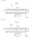
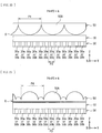
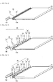
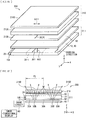
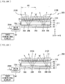
- FIG 1 illustrates a cross-sectional configuration of an illumination unit 1 according to a first embodiment of the present technology.
- the illumination unit 1 is applicable as a backlight of a display apparatus, and is allowed to output illumination light.
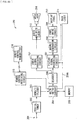
- the illumination unit 1 may include, for example, a light guide plate 10, a light source 20, a light modulation device 30, a reflection plate 40, a lens sheet 50, and a drive circuit 60.
- the light source 20 may be arranged on a side surface of the light guide plate 10.
- the light modulation device 30 may be arranged inside the light guide plate 10.
- the reflection plate 40 may be arranged on the back of the light guide plate 10.
- the lens sheet 50 may be arranged above the light guide plate 10.
- the drive circuit 60 may drive the light modulation device 30.
- the light guide plate 10 corresponds to a specific example of "first substrate” or “second substrate” in the present technology.
- the light source 20 corresponds to a specific example of "light source” in the present technology.
- An optical system configured of the light source 20, the light modulation device 30, and the reflection plate 40 corresponds to a specific example of "illumination optical system” in the present technology.
- the light guide plate 10 guides light from the light source 20 arranged on the side surface of the light guide plate 10 toward a top surface of the light guide plate 10 (specifically, a light exiting surface 1A of the illumination unit 1).
- the light guide plate 10 may have, for example, a shape corresponding to a subject to be illuminated (for example, a display panel 210 which is described later) that is arranged on the top surface of the light guide plate 10.
- the light guide plate 10 may have a cuboid shape that is surrounded by a top surface, a bottom surface, and side surfaces. It is to be noted that, out of the side surfaces of the light guide plate 10, the side surface which the light from the light source 20 enters is referred to as a light entering surface 10A below.
- the light guide plate 10 may have, for example, a shape having a predetermined pattern on one or both of the top surface and the bottom surface.
- the light guide plate 10 may have, for example, a function of scattering and uniformizing light entered from the light entering surface 10A. It is to be noted that, in a case where luminance is uniformized by modulating a voltage to be applied to the light modulation device 30, a flat light guide plate that has not been patterned may be used as the light guide plate 10.
- the light guide plate 10 may be, for example, a transparent substrate that mainly includes a transparent thermoplastic resin such as a polycarbonate resin (PC) or an acrylic resin (polymethylmethacrylate (PMMA)).
- PC polycarbonate resin
- PMMA polymethylmethacrylate
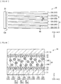
- the light source 20 is a linear light source, and may be configured, for example, of a hot cathode fluorescent lamp (HCFL), a cold cathode fluorescent lamp (CCFL), a plurality of LEDs (Light Emitting Diodes) arranged in a line, or the like. In a case where the light source 20 is configured of the plurality of LEDs, all of the LEDs may be preferably configured of white LEDs in view of efficiency, reduction in thickness, and uniformity. It is to be noted that, the light source 20 may include a red LED, a green LED, and a blue LED, for example. The light source 20 may be provided only on one side surface of the light guide plate 10 (see FIG. 1 ), or may be provided on two side surfaces, three side surfaces, or all of the side surfaces of the light guide plate 10.
- HCFL hot cathode fluorescent lamp
- CCFL cold cathode fluorescent lamp
- LEDs Light Emitting Diodes
- the light modulation device 30 is closely attached to inside of the light guide plate 10 with no air layer in between.
- the light modulation device 30 may be adhered to the light guide plate 10 with an adhesive (not illustrated) in between, for example.
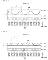
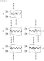
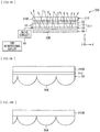
- the light modulation device 30 may include, for example, a transparent substrate 31, a bottom electrode 32, an alignment film 33, a light modulation layer 34, an alignment film 35, a top electrode 36, and a transparent substrate 37 that are arranged in order from the reflection plate 40.
- FIG 2 illustrates a cross-sectional configuration example of the light modulation device 30.
- the bottom electrode 32 and the top electrode 36 correspond to a specific example of "electrode" in the present technology.
- the light modulation layer 34 corresponds to a specific example of "light modulation layer” in the present technology.
- the transparent substrates 31 and 37 are arranged to be separated from each other and to be opposed to each other.
- the transparent substrates 31 and 37 support the light modulation layer 34.
- each of the transparent substrates 31 and 37 may be configured of a substrate transparent with respect to visible light such as a glass plate or a plastic film.
- the top electrode 36 and the bottom electrode 32 are configured to generate an electric field that generates, in the light modulation layer 34, a plurality of dot-like scattering regions that are arranged side by side in a plurality of lines or a plurality of linear scattering regions in a three-dimensional mode.
- the top electrode 36 and the bottom electrode 32 are configured to generate an electric field that generates, in the light modulation layer 34, a planar scattering region or a plurality of dot-like scattering regions that are arranged side by side in a matrix in a two-dimensional display mode. It is to be noted that the linear scattering region, the dot-like scattering region, and the planar scattering region are described in detail when description of the light modulation layer 34 is provided.
- the top electrode 36 is provided on a surface, of the transparent substrate 37, that is opposed to the transparent substrate 31.
- the top electrode 36 may be configured, for example, of one sheet-like electrode (continuous film) that is formed over the entire inside of the surface.
- the bottom electrode 32 is provided on a surface, of the transparent substrate 31, that is opposed to the transparent substrate 37.
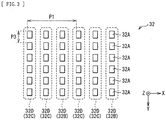
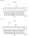
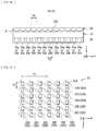
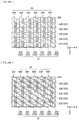
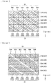
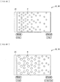
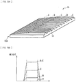
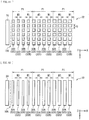
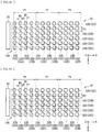
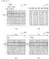
- the bottom electrode 32 may be configured, for example, of a plurality of partial electrodes 32A. It is to be noted that FIG. 3 illustrates a planar configuration example of the bottom electrode 32.
- each of the partial electrodes 32A may have a block shape, and the partial electrodes 32A may be arranged in a matrix, for example.
- the partial electrodes 32A may be arranged side by side in a direction parallel to the light entering surface 10A, and may be also arranged side by side in a direction orthogonal to the light entering surface 10A, for example.
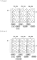
- an arrangement direction (direction orthogonal to the light entering surface 10A) of the linear electrode 32D corresponds to a parallax direction at the time of performing three-dimensional display.
- the bottom electrode 32 is configured to generate an electric field that generates, with respect to the light modulation layer 34, a plurality of lines of linear scattering regions (or a plurality of dot-like scattering regions that are arranged side by side in a line), when three-dimensional display is performed in the display apparatus (in the three-dimensional display mode).
- a plurality of specific linear electrodes 32D (hereinafter, referred to as "linear electrodes 32B") out of the linear electrodes 32D are configured to generate an electric field that generates, in the light modulation layer 34, a plurality of dot-like scattering regions that are arranged side by side in a line or a linear scattering region in the three-dimensional display mode.
- the linear electrodes 32B are arranged at a pitch P1 (a pitch same as a pitch P2 of the pixels or a pitch similar thereto) that corresponds to the pitch P2 (see FIG. 97 ) of the pixels at the time when three-dimensional display is performed in the display apparatus.
- a plurality of linear electrodes 32D that are electrodes excluding the linear electrodes 32B from the linear electrodes 32D are configured to generate, together with the linear electrodes 32B, an electric field that generates, with respect to the light modulation layer 34, a planar scattering region or a plurality of dot-like scattering regions that are arranged side by side in a matrix when two-dimensional display is performed in the display apparatus (in the two-dimensional display mode).
- all of the partial electrodes 32A are used in order to generate the planar scattering region or the plurality of dot-like scattering regions that are arranged side by side in a matrix with respect to the light modulation layer 34.
- illumination light generated in response to drive of the linear electrodes 32B is seen as linear light or dot-like light depends on a size of a pitch P3 of a plurality of partial electrodes 32A included in the linear electrode 32D.
- the scattering region inside the light modulation layer 34 is to be a light emitting region when light propagates inside the scattering region as described later.
- the linear electrodes 32B are used to generate a plurality of dot-like illumination light rays that are arranged side by side in a line or a linear illumination light ray in the three-dimensional display mode.
- all of the linear electrodes 32D are used to generate a planar illumination light ray or a plurality of dot-like illumination light rats that are arranged in a matrix in the two-dimensional display mode.
- the linear electrodes 32B and the linear electrodes 32C are arranged regularly in the direction orthogonal to the light entering surface 10A. As illustrated in FIGs. 2 and 3 , for example, a plurality of sets of linear electrode groups may be arranged in the direction orthogonal to the light entering surface 10A where one set is configured of one linear electrode 32B and two linear electrodes 32C. A width of the linear electrode 32B may be, for example, smaller than a width of the pixel in the display apparatus. It is to be noted that the linear electrode group may not always configured of one linear electrode 32B and two linear electrodes 32C, and may be configured of one linear electrode 32B and three linear electrodes 32C, for example, which is not illustrated.
- the bottom electrode 32 and the top electrode 36 may be each configured of an optically-transmissive conductive film (or a transparent conductive film).
- the optically-transmissive conductive film (or the transparent conductive film) may be configured, for example, of ITO. It is to be noted that the bottom electrode 32 and the top electrode 36 may be each configured of indium zinc oxide (IZO), metal nanowire, carbon nanotube, graphene, etc.
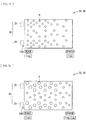
- each light modulation cell 30-1 corresponds to a specific example of "dot-like scattering region" in the present technology.
- a cell configured of a plurality of light modulation cells 30-1 that are arranged side by side in a line corresponds to a specific example of "linear scattering region” or "a plurality of dot-like scattering regions that are arranged side by side in a line” in the present technology.
- a cell configured of all light modulation cells 30-1 corresponds to a specific example of "planar scattering region” or "a plurality of dot-like scattering regions that are arranged side by side in a matrix” in the present technology.
- the light modulation cell 30-1 corresponds to a portion, of the light modulation device 30, that corresponds to a place where the bottom electrode 32 and the top electrode 36 are opposed to each other.
- a light modulation cell 30a (see FIG. 2 ) that includes the linear electrode 32B out of the light modulation cells 30-1 is used to generate a linear illumination light ray or a plurality of dot-like illumination light rays that are arranged side by side in a line.
- a light modulation cell 30b (see FIG 2 ) that includes the linear electrode 32C out of the light modulation cells 30-1 is used to generate a planar illumination light ray, together with the light modulation cells 30a.
- all of the light modulation cells 30-1 are used to generate a plurality of dot-like illumination light rays that are arranged in a matrix or the planar illumination light ray.
- the respective modulation cells 30-1 are allowed to be driven separately and independently by applying a predetermined voltage to the partial electrodes 32A and the top electrode 36.
- Each of the respective light modulation cells 30-1 exhibits transparent characteristics or scattering characteristics with respect to light from the light source 20, depending on magnitude of a value of a voltage to be applied to the partial electrode 32A and the top electrode 36. It is to be noted that the transparent characteristics and the scattering characteristics are described in detail when description of the light modulation layer 34 is provided.
- Each of the alignment films 33 and 35 may align liquid crystal or monomers used for the light modulation layer 34, for example.
- Examples of kinds of the alignment film may include a vertical alignment film and a horizontal alignment film.
- the horizontal alignment film is used for each of the alignment films 33 and 35 in the present embodiment.
- Examples of the horizontal alignment film may include an alignment film that is formed by performing a rubbing process on polyimide, polyamide imide, polyvinyl alcohol, etc. and an alignment film provided with a groove shape by transferring, etching, etc.
- Examples of the horizontal alignment film may further include an alignment film formed by obliquely depositing an inorganic material such as silicon oxide, a diamond-like carbon alignment film formed by ion beam irradiation, and an alignment film formed with an electrode pattern slit.
- a firing temperature after applying the alignment films 33 and 35 onto surfaces of the transparent substrates 31 and 37 may be preferably as low as possible in a manufacturing process.
- polyamide imide that is allowed to be formed at a temperature of 100°C or lower may be preferably used for each of the alignment films 33 and 35.
- the vertical alignment film and the horizontal alignment film it is enough that a function of aligning liquid crystal and monomers is provided, and reliability based on repeated application of voltages which is required in a usual liquid crystal display, etc. are not necessary, because reliability based on voltage application after forming a device is determined by an interface of polymerized monomers and liquid crystal.
- electrodes may be formed separately for alignment and driving, or dual-frequency liquid crystal having a sign of dielectric constant anisotropy that is inverted depending on frequency may be used as a liquid crystal material.
- a material that has large magnetic susceptibility anisotropy may be preferably used as the alignment film.
- a material that has a large number of benzene rings may be preferably used.
- the light modulation layer 34 is provided in a gap between the transparent substrate 31 and the transparent substrate 37.
- the light modulation layer 34 exhibits scattering characteristics or transparent characteristics with respect to light from the light source 20, depending on magnitude of an electric field.
- the light modulation layer 34 exhibits the transparent characteristics with respect to the light from the light source 20 when the electric field is relatively small, and the light modulation layer 34 exhibits scattering characteristics with respect to the light from the light source 20 when the electric field is relatively large.
- the light modulation layer 34 may be configured, for example, of a composite layer that includes a bulk 34A and a plurality of microparticulate microparticles 34B that are dispersed in the bulk 34A.
- the bulk 34A and the microparticles 34B have optical anisotropy.
- FIG. 4A schematically illustrates an example of an alignment state inside the microparticles 34B at the time when no voltage is applied between the bottom electrode 32 and the top electrode 36. It is to be noted that illustration of an alignment state inside the bulk 34A is omitted in FIG. 4A.
- FIG. 4B illustrates an example of a refractive index ellipsoid that shows refractive index anisotropy of the bulk 34A and the microparticles 34B at the time when no voltage is applied between the bottom electrode 32 and the top electrode 36.
- the refractive index ellipsoid illustrates, using a tensor ellipsoid, a refractive index of linear polarized light that has entered from various directions.
- FIG 4C schematically illustrates an example of a state in which light L1 that travels in a front direction and light L2 that travels in an oblique direction pass through the light modulation layer 34 at the time when no voltage is applied between the bottom electrode 32 and the top electrode 36.
- FIG 5A schematically illustrates an example of the alignment state inside the microparticles 34B at the time when a voltage is applied between the bottom electrode 32 and the top electrode 36. It is to be noted that illustration of an alignment state inside the bulk 34A is omitted in FIG. 5A.
- FIG. 5B illustrates an example of a refractive index ellipsoid that shows the refractive index anisotropy of the bulk 34A and the microparticles 34B at the time when a voltage is applied between the bottom electrode 32 and the top electrode 36.
- FIG. 5A schematically illustrates an example of the alignment state inside the microparticles 34B at the time when a voltage is applied between the bottom electrode 32 and the top electrode 36.
- 5C schematically illustrates an example of a state in which the light L1 that travels in the front direction and the light L2 that travels in the oblique direction are scattered in the light modulation layer 34 at the time when a voltage is applied between the bottom electrode 32 and the top electrode 36.
- the bulk 34A and the microparticle 34B may have a configuration in which a direction of an optical axis AX1 of the bulk 34A and a direction of an optical axis AX2 of the microparticle 34B coincide with (are parallel to) each other when no voltage is applied between the bottom electrode 32 and the top electrode 36, for example.
- the optical axes AX1 and AX2 each refer to a line parallel to a traveling direction of a light ray having a refractive index that has one value irrespective of polarization direction.
- the directions of the optical axis AX1 and the optical axis AX2 do not necessarily coincide with each other.
- the direction of the optical axis AX1 and the direction of the optical axis AX2 may be different for some extent because of a manufacturing error, etc., for example.
- the microparticle 34B may have a configuration in which the optical axis AX2 becomes parallel to the light entering surface 10A of the light guide plate 10 when no voltage is applied between the bottom electrode 32 and the top electrode 36, for example.
- the microparticle 34B may further have a configuration in which the optical axis AX2 intersects with the surfaces of the transparent substrates 31 and 37 at a slight angle ⁇ 1 when no voltage is applied between the bottom electrode 32 and the top electrode 36, for example (see FIG. 4B ).
- the angle ⁇ 1 is described in detail when description of a material configuring the microparticle 34B is provided.
- the bulk 34A may have a configuration in which the optical axis AX1 of the bulk 34A is constant irrespective of whether or not a voltage is applied between the bottom electrode 32 and the top electrode 36, for example.
- the bulk 34A may have a configuration in which the optical axis AX1 of the bulk 34A is parallel to the light entering surface 10A of the light guide plate 10 and intersects with the surfaces of the transparent substrates 31 and 37 at the predetermined angle ⁇ 1, for example.
- the optical axis AX1 of the bulk 34A is parallel to the optical axis AX2 of the microparticle 34B when no voltage is applied between the bottom electrode 32 and the top electrode 36.
- the optical axis AX2 is not necessarily parallel to the light entering surface 10A and does not necessarily intersect with the surfaces of the transparent substrates 31 and 37 at the angle ⁇ 1.
- the optical axis AX2 may intersect with the surfaces of the transparent substrates 31 and 37 at an angle slightly different from the angle ⁇ 1 because of a manufacturing error, etc., for example.
- the optical axes AX1 and AX2 are not necessarily parallel to the light entering surface 10A.
- the optical axes AX1 and AX2 may intersect with the light entering surface 10A at a small angle because of a manufacturing error, etc., for example.
- an ordinary refractive index of the bulk 34A and an ordinary refractive index of the microparticle 34B may be preferably equal to each other, and an extraordinary refractive index of the bulk 34A and an extraordinary refractive index of the microparticle 34B may be preferably equal to each other.
- little refractive index difference is caused in all directions including the front direction and the oblique direction, and high transparent characteristics are achieved when no voltage is applied between the bottom electrode 32 and the top electrode 36, for example.
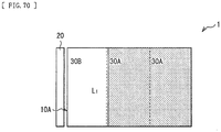
- the light L1 traveling in the front direction and the light L2 traveling in the oblique direction may not be scattered inside the light modulation layer 34 and may pass through the light modulation layer 34, for example.
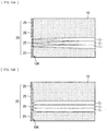
- the light L (light from the oblique direction) from the light source 20 may be totally reflected by an interface (a bottom surface of the transparent substrate 31 and a top surface of the light guide plate 10) of a transparent region (transmission region 30A) in the light modulation layer 34, and luminance (luminance in black display) in the transmission region 30A may be decreased, compared to that in a case where the entire surface is caused to emit light uniformly (a dashed-dotted line illustrated in FIG 6B ).
- a profile of front luminance illustrated in FIG. 6B is obtained by providing a diffusion sheet (not illustrated) on the light guide plate 10 and measuring the front luminance through the diffusion sheet.
- the top surface (light exiting surface 10B in FIG. 6 ) of the light guide plate 10 that is one of the interfaces of the transmission region 30A may be preferably in contact with a material having a refractive index that is lower than a refractive index of the top surface of the light guide plate 10.
- a typical example of such a low refractive index material may be air.
- the low refractive index material to be in contact with the top surface of the light guide plate 10 may be a gluing agent or an adhesive.
- the bulk 34A and the microparticle 34B may have a configuration in which the directions of the optical axis AX1 and the optical axis AX2 are different from each other (intersect with each other or are almost orthogonal to each other) when a voltage is applied between the bottom electrode 32 and the top electrode 36, for example.
- the microparticle 34B may have a configuration in which the optical axis AX2 of the microparticle 34B is parallel to the light entering surface 10A of the light guide plate 10 and intersects with the surfaces of the transparent substrates 31 and 37 at an angle ⁇ 2 (for example, 90°) that is larger than the angle ⁇ 1 when a voltage is applied between the bottom electrode 32 and the top electrode 36, for example.
- angle ⁇ 2 is described in detail when description is provided of the material configuring the microparticle 34B.
- the light L1 traveling in the front direction and the light L2 traveling in the oblique direction may be scattered inside the light modulation layer 34, for example.
- FIG. 5C illustrates that the light L1 traveling in the front direction and the light L2 traveling in the oblique direction may be scattered inside the light modulation layer 34, for example.
- the light L (light from the oblique direction) from the light source 20 may pass through an interface (an interface between air and the transparent substrate 31 or the light guide plate 10) of a scattering region 30B, and light that has passed through to the reflection plate 40 side may be reflected by the reflection plate 40 and may pass through the light modulation device 30, for example.
- luminance in the scattering region 30B becomes extremely higher compared to that in the case where the entire surface is caused to emit light uniformly (the dashed-dotted line illustrated in FIG. 6B ).
- luminance in partial white display is increased as the luminance in the transmission region 30A is decreased.
- the ordinary refractive indices of the bulk 34A and the microparticle 34B may be different in some extent because of a manufacturing error, etc., for example.
- the difference therebetween may be preferably 0.1 or smaller, and may be more preferably 0.05 or smaller, for example.
- the extraordinary refractive indices of the bulk 34A and the microparticle 34B may be also different in some extent because of a manufacturing error, etc., for example.
- the difference therebetween may be preferably 0.1 or smaller, and may be more preferably 0.05 or smaller, for example.
- Such refractive index differences may be preferably 0.05 or larger, more preferably 0.1 or larger, and still more preferably 0.15 or larger.
- the bulk 34A and the microparticle 34B are different from each other in response speed with respect to an electric field.
- the bulk 34A may have a streaky structure, a porous structure, or a rod-like structure that has response speed slower than response speed of the microparticle 34B, for example.
- the bulk 34A may be formed, for example, of a polymer material that is obtained by polymerizing low-molecular monomers.
- the bulk 34A may be formed, for example, by polymerizing, with the use of one or both of heat and light, materials (for example, monomers) that are aligned along the alignment direction of the microparticle 34B or the alignment directions of the alignment films 33 and 35 and has alignment characteristics and polymerization characteristics.
- the streaky structure, the porous structure, or the rod-like structure of the bulk 34A may have a major axis in a direction that is parallel to the light entering surface 10A of the light guide plate 10 and intersects with the surfaces of the transparent substrates 31 and 37 at the slight angle ⁇ 1, for example.
- an average streaky composition size in a minor-axis direction may be preferably from 0.1 ⁇ m to 10 ⁇ m both inclusive, and may be more preferably in a range from 0.2 ⁇ m to 2.0 ⁇ m both inclusive, in view of increase in scattering characteristics of guided light.
- the scattering performance inside the light modulation device 30 becomes about the same in a visible region from 380 nm to 780 nm. For this reason, it does not happen that only light having a specific wavelength component is increased or decreased in a plane, which achieves valance in the visible region in the plane.
- the scattering performance of the light modulation device 30 is low irrespective of wavelength, which makes it more difficult for the light modulation device 30 to serve as a light modulation device.
- the average streaky composition size in the minor-axis direction may be preferably in a range from 0.5 ⁇ m to 5 ⁇ m both inclusive, and more preferably in a range from 1 ⁇ m to 3 ⁇ m.
- wavelength dependency of scattering in the bulk 34A is suppressed when the light emitted from the light source 20 repeatedly passes through the bulk 34A inside the light modulation device 30 in a process that the light emitted from the light source 20 propagates inside the light guide plate 10.
- the size of the streaky composition is allowed to be observed with the use of a polarization microscope, a confocal microscope, an electron microscope, or the like.
- the microparticle 34B may mainly include a liquid crystal material, and may have response speed that is sufficiently faster than the response speed of the bulk 34A, for example.
- the liquid crystal material (liquid crystal molecule) included inside the microparticle 34B may be, for example, a rod-like molecule.
- a liquid crystal molecule that has positive dielectric constant anisotropy (so-called positive liquid crystal) may be preferably used as the liquid crystal molecule included inside the microparticle 34B.
- the major-axis direction of the liquid crystal molecule is parallel to the optical axis AX1 inside the microparticle 34B when no voltage is applied between the bottom electrode 32 and the top electrode 36.
- the major-axis of the liquid crystal molecule inside the microparticle 34B is parallel to the light entering surface 10A of the light guide plate 10 and intersects with the surfaces of the transparent substrates 31 and 37 at the slight angle ⁇ 1.
- the liquid crystal molecule inside the microparticle 34B is aligned to be tilted at the angle ⁇ 1 in a plane parallel to the light entering surface 10A of the light guide plate 10 when no voltage is applied between the bottom electrode 32 and the top electrode 36.
- the angle ⁇ 1 is referred to as a pre-tilt angle, and may be preferably in a range from 0.1° to 30° both inclusive, for example.
- the angle ⁇ 1 may be more preferably in a range from 0.5° to 10° both inclusive, and still more preferably in a range from 0.7° to 2° both inclusive.
- the angle ⁇ 1 is increased, efficiency in scattering tends to be decreased for a reason described later.
- the angle ⁇ 1 is made excessively small, variations are caused in an azimuth at which liquid crystal rises upon voltage application. For example, liquid crystal may rise at an azimuth in a 180-degree opposite direction (reverse tilt). This prevents effective utilization of the refractive index difference between the microparticle 34B and the bulk 34A. Accordingly, scattering efficiency is decreased, and luminance tends to be decreased.
- the major-axis direction of the liquid crystal molecule intersects with (or is orthogonal to) the optical axis AX1 inside the microparticle 34B.
- the major axis of the liquid crystal molecule inside the microparticle 34B is parallel to the light entering surface 10A of the light guide plate 10 and intersects with the surfaces of the transparent substrates 31 and 37 at the angle ⁇ 2 (for example, 90°) that is larger than the angle ⁇ 1.
- any material may be used as long as the material optically has anisotropy and is capable of forming a composite with liquid crystal; however, a ultraviolet-curable low-molecular monomer may be preferably used in the present embodiment. Because a direction of optical anisotropy of liquid crystal may preferably coincide with a direction of optical anisotropy of a material (polymer material) formed by polymerizing low-molecular monomers in a state where no voltage is applied, the liquid crystal and the low-molecular monomers may be preferably aligned in the same direction before performing ultraviolet curing.
- the monomer material to be used may preferably have a rod-like shape.
- a material that has both polymerization characteristics and liquid crystal characteristics may be preferably used as the monomer material.
- the material may preferably have one or more functional groups selected from the group consisting of an acrylate group, a methacrylate group, an acryloyloxy group, a methacryloyloxy group, a vinylether group, and an epoxy group, as a polymerizable functional group. These functional groups are allowed to be polymerized by applying ultraviolet rays, infrared rays, or electron rays, by heating, etc.
- a liquid crystal material having a multi-functional group may be added in order to suppress decrease in alignment degree at the time of applying ultraviolet rays.
- a bi-functional liquid crystalline monomer may be preferably used as a raw material of the bulk 34A.
- a mono-functional monomer may be added to the raw material of the bulk 34A in order to adjust temperature at which liquid crystal characteristics are exhibited, or a tri-or-more-functional monomer may be added thereto in order to improve crosslink density.
- the reflection plate 40 causes light that has leaked from the back of the light guide plate 10 through the light modulation device 30 to return toward the light guide plate 10.
- the reflection plate 40 may have, for example, functions such as reflection, diffusion, and scattering. This allows efficient utilization of light emitted from the light source 20, and also contributes to improvement in front luminance.
- the reflection plate 40 may be configured, for example, of foamed PET (polyethylene terephthalate), a silver-deposited film, a multi-layered reflection film, white PET, or the like.
- the reflection plate 40 may be preferably configured, for example, of the silver-deposited film, the multi-layered reflection film, an aluminum-deposited film, or the like. Further, the reflection plate 40 may have a shape for reflecting light in a particular direction.
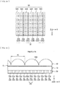
- the lens sheet 50 reduces a divergence angle of light (illumination light) that exits from the top surface of the light guide plate 10.
- the lens sheet 50 may be arranged above the light guide plate 10 so that a gap G is formed between a light entering surface (bottom surface) of the lens sheet 50 and the light exiting surface (top surface) of the light guide plate 10.
- the gap G is a layer filled with a material that has a refractive index smaller than a refractive index of the light exiting surface (top surface) of the light guide plate 10, and may be an air layer, for example. It is to be noted that the gap G may not be necessarily an air layer.
- the gap G may be a layer filled with a gluing agent or an adhesive that is configured of the material that has a refractive index smaller than a refractive index of the light exiting surface (top surface) of the light guide plate 10.
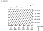
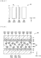
- the lens sheet 50 may have a concave-convex surface in which a plurality of convex portions 50A are arranged in a matrix in a plane, for example.
- the convex portion 50A corresponds to a specific example of "lens" in the present technology.
- the concave-convex surface may be arranged on the light exiting side of the lens sheet 50, for example.
- the concave-convex surface may be arranged on the light entering side (on the light modulation layer 34 side) of the lens sheet 50. Light having a shallower angle out of the light exited from the light guide plate 10 is allowed to rise vertically in the case where the concave-convex surface is arranged on the light entering side of the lens sheet 50.
- a surface opposite from the concave-convex surface may be a flat surface as illustrated in FIGs. 7 and 8 , for example.
- the flat surface of the lens sheet 50 may be adhered directly onto a display panel (or a polarizing plate) with the use of a gluing agent or an adhesive.
- the convex portions 50A are formed of a UV-curable resin or the like, the concave portions 50A may be formed directly on the display panel (or the polarizing plate).
- the lens sheet 50 may be arranged so that the above-described flat surface is parallel or almost parallel to the top surface of the light guide plate 10, for example.
- the convex portions 50A are arranged side by side in a direction parallel to an extending direction of the linear electrode 32D, and are also arranged side by side in a direction intersecting with the extending direction of the linear electrode 32D. It is to be noted that, when the light modulation cell 30a is in a scattering state, the light modulation cell 30a serves as a dot-like scattering region.
- the convex portions 50A are arranged side by side in a direction parallel to an extending direction of the linear scattering region or an arrangement direction of the dot-like scattering regions that are arranged side by side in a line, and are also arranged side by side in a direction intersecting with the extending direction of the linear scattering region or the arrangement direction of the dot-like scattering regions that are arranged side by side in a line.
- the convex portion 50A may include a curved surface.
- a light exiting surface of the convex portion 50A may be configured only of a curved surface, or may be configured of a composite surface of a curved surface and a planar surface or a polyangular surface.
- the light entering surface of the convex portion 50A may be configured only of a curved surface, or may be configured of a composite surface of a curved surface and a planar surface or a polyangular surface.
- the convex portion 50A has a convex shape that protrudes on the light exiting side of the lens sheet 50 in the case where the convex portion 50A is arranged on the light exiting side of the lens sheet 50.
- the convex portion 50A has a convex shape that protrudes on the light entering side of the lens sheet 50 in the case where the convex portion 50A is arranged on the light entering side of the lens sheet 50.
- the convex portion 50A is arranged so that an apex position of the convex portion 50A is to be opposed to the bottom electrode 32 (or the light modulation cell 30a).
- the light modulation cell 30a is a dot-like scattering region when the light modulation cell 30a is in a scattering state. Accordingly, at this time, the convex portion 50A is arranged so that the apex position of the convex portion 50A is opposed to the linear scattering region or to the dot-like scattering regions that are arranged side by side in a line.
- the respective convex portions 50A may be preferably arranged so that each of the convex portions 50A corresponds to one of the dot-like scattering regions in a one-to-one relationship.
- the convex portion 50A may preferably has rotational symmetry having center at an apex of the convex portion 50A.
- the convex portion 50A may preferably have four-fold rotational symmetry having center at the apex of the convex portion 50A.
- the convex portion 50A may preferably have two-fold rotational symmetry having center at the apex of the convex portion 50A.
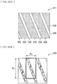
- the curved surface of the convex portion 50A may have, for example, a stereoscopic shape in which a cross-section perpendicular to the Y-axis in the drawing or a cross-section perpendicular to the X-axis in the drawing has a cylindrical shape illustrated in FIG. 9A or 9B .
- the curved surface of the convex section 50A may have a true spherical shape or an aspherical shape, or may have an ellipsoidal spherical shape, a paraboloidal shape, or a hyperboloidal shape, for example, which is not illustrated.
- a first cross-section (the cross-section perpendicular to the Y-axis in the drawing or the cross-section perpendicular to the X-axis in the drawing) of the convex portion 50A may have a true circle shape, an ellipsoid shape, a parabolic shape, or a hyperbolic shape.
- FIGs. 7 and 8 illustration is made as if two ridge lines intersecting with each other are present on the curved surface of the convex portion 50A; however, the ridge lines are provided for convenience in order to express the shape of the convex portion 50A.
- FIGs. 7 and 8 therefore do not mean that such ridge lines are necessarily present on the curved surface of the convex portion 50A.
- the entire curved surface of the convex portion 50A may be configured only of a smooth curved surface.
- a focal length of the convex portion 50A is allowed to be longer. Accordingly, it is possible to allow a distance between the light modulation cell 30a and the convex portion 50A to be longer as the focal length of the convex portion 50A becomes longer, which increases freedom in design of thicknesses of the light guide plate 10, the transparent substrate 37, etc.
- the first cross-section (the cross-section perpendicular to the Y-axis in the drawing) of the convex portion 50A and the second cross-section (the cross-section perpendicular to the X-axis in the drawing) of the convex portion 50A may have shapes different from each other.
- the curved surface of the convex portion 50A may be that expressed by an anamorphic aspherical surface expression in Expression 1, for example.
- Rx is a curvature radius, of the convex portion 50A, in a direction orthogonal to the extending direction of the linear electrode 32D.
- Ry is a curvature radius, of the convex portion 50A, in a direction parallel to the extending direction of the linear electrode 32D.
- kx is a conic constant in the X-axis direction.
- ky is a conic constant in the Y-axis direction.
- the curved surface of the convex portion 50A corresponds to a shape in a case where -1 ⁇ kx ⁇ 0 is established in Expression 1.
- the curved surface of the convex portion 50A corresponds to a shape in a case where kx ⁇ -1 is established in Expression 1.
- -40 ⁇ kx ⁇ 0 may be preferably established, and -30 ⁇ kx ⁇ -4 may be more preferably established.
- the curved surface of the convex portion 50A corresponds to a shape in a case where -1 ⁇ ky ⁇ 0 is established in Expression 1.
- the curved surface of the convex portion 50A corresponds to a shape in a case where ky ⁇ -1 is established in Expression 1.
- -40 ⁇ ky ⁇ 0 may be preferably established, and -30 ⁇ ky ⁇ -4 may be more preferably established.
- FIGs. 10 to 17 each illustrate an example of a cross-sectional configuration of the lens sheet 50 together with the light guide plate 10 and the light modulation device 30.
- FIGs. 10 to 17 each illustrate the cross-sectional configuration example in an XZ plane.
- FIGs. 10 to 17 each illustrate, as an example, a case where the ridge line of the first cross-section of the convex portion 50A has a true circle shape. However, description below is also applicable to a case where the ridge line of the first cross-section of the convex portion 50A has a shape other than the true circle shape.
- the pitch P2 of the concave-convex surface may be PI, for example.
- the widths of the respective convex portions 50A may not be necessarily equal to one another.
- the convex portion 50A having a larger width and the convex portion 50A having a smaller width may be arranged alternately.
- the convex portion 50A having a larger width may be preferably arranged at a position that is opposed to the light modulation cell 30a.
- the pitch P2 of the concave-convex surface may be, for example, P1/2 as illustrated in FIGs. 12 and 13 , or may be, for example, P1/4 as illustrated in FIGs. 16 and 17 .
- the respective convex portions 50A may be preferably arranged so that each of the convex portions 50A corresponds to one of the partial electrodes 32A in a one-to-one relationship as illustrated in FIG. 18 , for example.
- a radius (the curvature radius Rx in a parallax direction at the time of performing three-dimensional display) of the convex portion 50A may be preferably P1/N ⁇ 0.6 ⁇ R ⁇ P1/N ⁇ 1.4 where P1 is the pitch of the light modulation cell 30a (a part that can be a linear scattering region), and N is the number of perspectives at the time of performing three-dimensional display. Moreover, the radius of the convex portion 50A may be more preferably P1/N ⁇ 0.8 ⁇ R ⁇ P1/N ⁇ 1.2.
- the convex portion 50A is arranged so that the middle of the convex portion 50A in the width direction is opposed to the light modulation cell 30a (a part that can be a scattering region).
- the convex portion 50A may be preferably arranged so that the middle of the convex portion 50A in the width direction is opposed to the middle of the light modulation cell 30a in the width direction.
- a distance Lz between the convex portion 50A and the light modulation cell 30a may be preferably 0 ⁇ Lz ⁇ Rx/(n2(n1-1)) ⁇ 1.4 where Rx is the curvature radius (the curvature radius in the parallax direction at the time of performing three-dimensional display) of the convex portion 50A, n1 is a refractive index of the convex portion 50A, and n2 is a refractive index between the convex portion 50A and the light modulation cell 30a.
- the distance Lz between the convex portion 50A and the light modulation cell 30a may be preferably Rx/(n2(n1-1)) ⁇ 0.7 ⁇ Lz ⁇ R/(n2(n1-1)) ⁇ 1.2. In such a case, luminance in the front direction is increased compared to that in a case where the distance Lz between the convex portion 50A and the light modulation cell 30a is out of the above-described range.
- the lens sheet 50 may be preferably configured of a material having an isotropic refractive index.
- the light exited from the top surface of the light guide plate 10 is polarized light that has a polarization axis in a direction parallel to the optical axis AX1 of the bulk 34A having low responsiveness to an electric field. Accordingly, for example, in a case where light emitted from the illumination unit 1 may be preferably polarized light in view of improvement in luminance of the display panel, the light exited from the top surface of the light guide plate 10 may be utilized as the emission light from the illumination unit 1 as it is without disturbing polarization.
- the lens sheet 50 may be preferably configured of the material having an isotropic refractive index in view of not disturbing the polarization component of the light exited from the top surface of the light guide plate 10.
- FIGs. 19 to 26 each illustrate another example of the cross-sectional configuration of the lens sheet 50, together with the light guide plate 10 and the light modulation device 30.
- FIGs. 19 to 26 each illustrate the cross-sectional configuration example in a YZ plane.
- FIGs. 19 to 26 each illustrate, as an example, a case where the cross-section, of the convex portion 50A, that is perpendicular to the X axis in the drawing has a true circle shape.
- description below is also applicable to a case where the cross-section, of the convex portion 50A, that is perpendicular to the X axis in the drawing has a shape other than the true circle shape.
- the pitch P4 of the concave-convex surface may be more preferably P3.
- the pitch P4 of the concave-convex surface may be P3 ⁇ N, for example.
- the widths of the respective convex portions 50A may not be necessarily equal to one another.
- the convex portion 50A having a larger width and the convex portion 50A having a smaller width may be arranged alternately.
- the pitch P4 of the concave-convex surface may be, for example, P3 ⁇ 2 as illustrated in FIGs. 23 and 24 , or may be, for example, P3 as illustrated in FIGs. 25 and 26 .
- the convex portions 50A arranged in a matrix may be preferably arranged at a position that is opposed to one of the partial electrodes 32A as illustrated in FIG. 18 , for example.
- the curvature radius Ry in a direction perpendicular to the parallax direction of the convex portion 50A at the time of performing three-dimensional display may be preferably P3 ⁇ 0.6 ⁇ Ry ⁇ P3 ⁇ 1.4, and may be more preferably P3 ⁇ 0.8 ⁇ Ry ⁇ P3 ⁇ 1.2.
- the convex portion 50A is arranged so that the middle of the convex portion 50A in the width direction is opposed to the light modulation cell 30a (a part that can be a linear scattering region).
- the convex portion 50A may be preferably arranged so that the middle of the convex portion 50A in the width direction is opposed to the middle of the light modulation cell 30a in the width direction.
- the distance Lz between the convex portion 50A and the light modulation cell 30a may be preferably 0 ⁇ Lz ⁇ Ry/(n2(n1-1)) ⁇ 1.4 where Ry is the curvature radius in the direction perpendicular to the parallax direction of the convex portion 50A at the time of performing three-dimensional display, n1 is the refractive index of the convex portion 50A, and n2 is the refractive index between the convex portion 50A and the light modulation cell 30a.
- the distance Lz between the convex portion 50A and the light modulation cell 30a may be preferably R/(n2(n1-1)) ⁇ 0.7 ⁇ Lz ⁇ Ry / (n2(n1-1)) ⁇ 1.2. In such a case, luminance in the front direction is increased compared to that in a case where the distance Lz between the convex portion 50A and the light modulation cell 30a is positioned at a place farther than the above-described range.
- the drive circuit 60 may control magnitude of a voltage to be applied to a pair of electrodes (the partial electrode 32A and the top electrode 36) of each of the light modulation cells 30-1 so that the optical axis AX2 of the microparticle 34B is parallel or almost parallel to the optical axis AX1 of the bulk 34A in one light modulation cell 30-1, and the optical axis AX2 of the microparticle 34B intersects with or is orthogonal to the optical axis AX1 of the bulk 34A in another light modulation cell 30-2, for example.
- the drive circuit 60 is configured to be capable of causing the directions of the optical axes AX1 and AX2 of the bulk 34A and the microparticle 34B to coincide with (or almost coincide with) each other or to be different from (or to be orthogonal to) each other by controlling an electric field.
- the drive circuit 60 causes a plurality of dot-like illumination light rats that are arranged side by side in a line or a plurality of linear illumination light rays to be outputted from the light modulation device 30 when a signal designating three-dimensional display is inputted as a control signal 20A (that is, in a three-dimensional display mode). Specifically, the drive circuit 60 applies a voltage causing the light modulation layer 34 to exhibit scattering characteristics to a plurality of specific partial electrodes 32B out of the partial electrodes 32A, and applies a voltage causing the light modulation layer 34 to exhibit transparent characteristics to a plurality of partial electrodes 32C that are electrodes excluding the partial electrodes 32B from the partial electrodes 32A.
- the drive circuit 60 controls the magnitude of the voltage to be applied to the pair of electrodes (the partial electrode 32A and the top electrode 36) of each of the light modulation cells 30-1 so that the optical axis AX2 of the microparticle 34B intersects with the optical axis AX1 of the bulk 34A in each of the light modulation cells 30a inside the light modulation device 30, and the optical axis AX2 of the microparticle 34B is parallel to the optical axis AX1 of the bulk 34A in the light modulation cell 30b inside the light modulation device 30.
- the drive circuit 60 generates the scattering region 30B in the light modulation cell 30a including the partial electrode 32B and generates the transmission region 30A in the light modulation cell 30b including the partial electrode 32C, and thereby causes the linear illumination light ray or the dot-like illumination light rays that are arranged side by side in a line to be outputted from the light modulation device 30.
- the drive circuit 60 causes a planar illumination light ray or a plurality of dot-like illumination light rays that are arranged side by side in a matrix to be outputted from the light modulation device 30 when a signal designating two-dimensional display is inputted as the control signal 20A (that is, in the two-dimensional display mode). Specifically, the drive circuit 60 applies a voltage causing the light modulation layer 34 to exhibit scattering characteristics to each of the partial electrodes 32A.
- the drive circuit 60 controls the magnitude of the voltage to be applied to the pair of electrodes (the partial electrode 32A and the top electrode 36) of each of the light modulation cells 30-1 so that the optical axis AX2 of the microparticle 34B intersects with or is orthogonal to (or almost orthogonal to) the optical axis AX1 of the bulk 34A in all of the light modulation cells 30-1 included in the light modulation device 30.
- the drive circuit 60 generates the scattering region 30B in each of the light modulation cells 30-1, and thereby causes the planar illumination light or the dot-like illumination lights that are arranged side by side in a matrix to be outputted from the light modulation device 30.
- a voltage is applied to the pair of electrodes (the partial electrode 32A and the top electrode 36) of each of the light modulation cells 30-1 so that the optical axis AX2 of the microparticle 34B intersects with or is orthogonal to the optical axis AX1 of the bulk 34A in each of the light modulation cells 30a, and the optical axis AX2 of the microparticle 34B is parallel or almost parallel to the optical axis AX1 of the bulk 34A in each of the light modulation cells 30b. Accordingly, each of the light modulation cells 30a becomes the scattering region 30B and each of the light modulation cells 30b becomes the transmission region 30A in the light modulation device 30.
- a linear illumination light ray or a plurality of dot-like illumination light rays that are arranged side by side in a line may be outputted in the front direction, for example.
- a voltage may be applied to the pair of electrodes (the partial electrode 32A and the top electrode 36) of each of the light modulation cells 30-1 so that the optical axis AX2 of the microparticle 34B intersects with or is orthogonal to the optical axis AX1 of the bulk 34A in each of the light modulation cells 30-1, for example. Accordingly, light that has been emitted from the light source 20 and has entered inside the light guide plate 10 is scattered in the scattering region 30B that is formed in the entire light modulation device 30.
- light that has passed through the bottom surface of the scattering region 30B is reflected by the reflection plate 40 to be returned again to the light guide plate 10, and then is caused to exit from the top surface of the illumination unit 1.
- light that has traveled toward the top surface of the scattering region 30B passes through the light guide plate 10, and then is caused to exit from the top surface of the illumination unit 1.
- light may be caused to exit from the entire top surface of the light modulation device 30, and a planar illumination light ray or a plurality of dot-like illumination light rays that are arranged side by side in a matrix may be outputted in the front direction, for example.
- the lens sheet 50 that reduces the divergence angle of illumination light is provided. This makes it possible to increase luminance in the front direction, compared to a case where no lens sheet 50 is provided. As a result, for example, in a case where the illumination unit 1 is used as a backlight of a display apparatus, it is possible to increase an amount of light that enters a display panel in the display apparatus at an angle from 0° to an appropriate viewing angle (for example, 15°), which achieves high luminance in the displayed picture.
- the illumination unit 1 of the present embodiment in a case where the partial electrodes 32A and the convex portions 50A are both arranged in a matrix, and the respective convex portions 50A are arranged so that each of the convex portions 50A corresponds to one of the partial electrodes 32A (or one of the dot-like scattering regions) in a one-to-one relationship, it is possible to reduce the divergence angle of the illumination light in the two arrangement directions (the X direction and the Y direction) of the convex portions 50A at the time of performing three-dimensional display. As a result, high luminance is achieved in a three-dimensional display picture.
- PDLC is formed by mixing a liquid crystal material and an isotropic low-molecular material and causing phase separation by application of ultraviolet rays, drying of a solvent, etc.
- PDLC is generally configured of a composite layer in which fine particles of the liquid crystal material are dispersed in a polymer material. When no voltage is applied, the liquid crystal material in the composite layer is aligned in a random direction, and therefore exhibits scattering characteristics. However, when a voltage is applied, the liquid crystal material is aligned in an electric field direction, and therefore exhibits high transparent characteristics in a front direction (a direction of a normal to PDLC) in a case where an ordinary reflective index of the liquid crystal material and a refractive index of the polymer material are equal to each other.
- a light modulation device using PDLC often has a structure in which PDLC is sandwiched between two glass plates each having a surface provided with a transparent conductive film.
- the light that has entered from the oblique direction is refracted due to a refractive index difference between the air and the glass plate, and therefore enters the PDLC at a smaller angle. Accordingly, large scattering is not caused in such a light modulation device. For example, in a case where light enters the light modulation device from the air at an angle of 80°, an entering angle of the light with respect to the PDLC is reduced to about 40° due to refraction at a glass interface.
- the bulk 34A and the microparticle 34B each mainly include an optically-anisotropic material, which reduces scattering characteristics in the oblique direction. Accordingly, it is possible to improve transparent characteristics.
- the bulk 34A and the microparticle 34B mainly include optically-anisotropic materials that have ordinary refractive indices equal to each other and extraordinary refractive indices equal to each other, and no voltage is applied between the bottom electrode 32 and the top electrode 36, the directions of these optical axes coincide or almost coincide with each other.
- the refractive index difference is reduced or eliminated in all directions including the front direction (the direction of the normal to the light modulation device 30) and the oblique direction, which achieves high transparent characteristics.
- the front direction the direction of the normal to the light modulation device 30
- the oblique direction which achieves high transparent characteristics.
- liquid crystal having an ordinary refractive index of 1.5 and an extraordinary refractive index of 1.65 and liquid crystalline monomers having an ordinary refractive index of 1.5 and an extraordinary refractive index of 1.65 are mixed, and the liquid crystalline monomers are polymerized in a state in which the liquid crystal and the liquid crystalline monomers are aligned by an alignment film or an electric field, the optical axis of the liquid crystal and the optical axis of a polymer formed by polymerization of the liquid crystalline monomers coincide each other.
- refractive indices it is possible to cause refractive indices to coincide one another in all directions. In such a case, it is therefore possible to achieve a state having high transparent characteristics, and to further improve viewing angle characteristics.
- luminance in black display in the transmission region 30A may be decreased compared to that in the case where the entire surface is caused to emit light uniformly (the dashed-dotted line in FIG. 8B ), for example.
- luminance in the scattering region 30B is extremely increased compared to that in a case where the entire surface is caused to emit light uniformly (the dashed-dotted line in FIG. 8B ).
- luminance in partial white display is increased as the luminance in the transmission region 30A is decreased.
- increase in luminance is a technology to increase luminance in a case where white display is partially performed compared to that in a case where white display is performed in the entire surface.
- This technology is often used in CRT, PDP, etc., generally.
- an entire backlight is caused to emit light uniformly irrespective of an image, and it is therefore not possible to partially increase luminance.
- the backlight is configured of a LED backlight in which a plurality of LEDs are arranged two-dimensionally, it is indeed possible to partially turn off the LEDs.
- the bulk 34A and the microparticle 34B mainly include the optically-anisotropic materials. Accordingly, scattering characteristics in the oblique direction is suppressed, and less light is leaked from the light guide plate in a dark state. For this reason, light is guided from a portion having a partial dark state to a portion having a partial bright state. It is therefore possible to achieve increase in luminance without increasing electric power to be supplied to the illumination unit 1.
- the optical axis AX2 of the microparticle 34B is parallel to the light entering surface 10A of the light guide plate 10 and intersects with the surfaces of the transparent substrates 31 and 37 at the slight angle ⁇ 1 in a region where no voltage is applied between the bottom electrode 32 and the top electrode 36.
- the liquid crystal molecule included inside the microparticle 34B is aligned to be tilted at the angle ⁇ 1 in a plane parallel to the light entering surface 10A (in a state provided with the pre-tilt angle).
- the liquid crystal material included inside the microparticle 34B does not rise at a random azimuth and rises in the plane parallel to the light entering surface 10A.
- the optical axes AX1 and AX2 of the bulk 34A and the microparticle 34B intersect with or are orthogonal to each other in the plane parallel to the light entering surface 10A.
- light that oscillates perpendicularly to the transparent substrate 31 is influenced by a difference between the extraordinary refractive index of the microparticle 34B and the ordinary refractive index of the bulk 34A.
- the difference between the extraordinary refractive index of the microparticle 34B and the ordinary refractive index of the bulk 34A is large, which causes scattering efficiency of the light that oscillates perpendicularly to the transparent substrate 31 to be increased.
- light that oscillates parallel to the transparent substrate 31 is influenced by a difference between the ordinary refractive index of the microparticle 34B and the extraordinary refractive index of the bulk 34A.
- the difference between the ordinary refractive index of the microparticle 34B and the extraordinary refractive index of the bulk 34A is also large, which causes scattering efficiency of the light that oscillates parallel to the transparent substrate 31 to be increased.
- light that propagates through a region in which a voltage is applied between the bottom electrode 32 and the top electrode 36 includes a lot of components in the oblique direction.
- light in a region in which a voltage is applied between the bottom electrode 32 and the top electrode 36 propagates at an angle of 41.8° or larger.
- the refractive index difference is increased in all directions including the oblique direction, and high scattering characteristics are therefore achieved. This makes it possible to improve display luminance. Also, it is possible to further improve display luminance due to the above-described effect of increase in luminance.
- the optical axes AX1 and AX2 of the bulk 34A and the microparticle 34B are arranged perpendicularly to the light entering surface 10A of the light guide plate 10 when no voltage is applied, and the liquid crystal material included inside the microparticle 34B is caused to rise in a plane perpendicular to the light entering surface 10A when a voltage is applied between the bottom electrode 32 and the top electrode 36, light that oscillates perpendicularly to the transparent substrate 31 is influenced by the difference between the extraordinary refractive index of the microparticle 34B and the ordinary refractive index of the bulk 34A similarly to in the above-described case, but light that oscillates in a direction parallel to the transparent substrate 31 is influenced by the difference between the ordinary refractive index of the microparticle 34B and the ordinary refractive index of the bulk 34A.
- the ordinary refractive index of the microparticle 34B there is little or no difference between the ordinary refractive index of the microparticle 34B and the ordinary refractive index of the bulk 34A. For this reason, in the light that has entered from the light entering surface 10A, the light that oscillates perpendicularly to the transparent substrate 31 is influenced by a large refractive index similarly to in the above-described case, but the light that oscillates in the direction parallel to the transparent substrate 31 is influenced little or is not influenced at all by the refractive index difference. As a result, scattering efficiency of the light that oscillates perpendicularly to the transparent substrate 31 is increased, but scattering efficiency of the light that oscillates parallel to the transparent substrate 31 is low or zero.
- each of the linear electrodes 32D extend in the direction parallel to the light entering surface 10A.
- each of the linear electrodes 32D may extend in a direction obliquely intersecting with the light entering surface 10A while the partial electrodes 32A have a layout same as that in the above-described embodiment.
- the respective convex portions 50A may be preferably arranged so that each of the convex portions 50A corresponds to one of the partial electrodes 32A in a one-to-one relationship, and may be more preferably so that each of the convex portions 50A is opposed to one of the partial electrodes 32A, for example. It is to be noted that each of the convex portions 50A has a rectangular shape in FIG. 20A ; however, as illustrated in FIG. 20B , each of the convex portions 50A may have a parallelogram shape or a rhomboid shape, for example.
- each of the linear electrodes 32D may extend in a direction orthogonal to the light entering surface 10A while the partial electrodes 32A have a layout same as that in the above-described embodiment.
- the respective convex portions 50A may be preferably arranged so that each of the convex portions 50A corresponds to one of the partial electrodes 32A in a one-to-one relationship, and may be more preferably so that each of the convex portions 50A is opposed to one of the partial electrodes 32A, for example.
- the extending direction of each of the linear electrodes 32D may preferably extend in a direction intersecting with the arrangement direction of pixels in the display panel 210 described later (see FIG. 94 described later). In such a case, it is possible to reduce a difference between resolution in a direction parallel to a normal to the light entering surface 10A and resolution in a direction parallel to the light entering surface 10A at the time of performing three-dimensional display.
- each of the partial electrodes 32A has a block shape.
- each of the partial electrodes 32A may have a strip-like shape.
- each of the partial electrodes 32A may extend in the direction parallel to the light entering surface 10A, and further, the partial electrodes 32A may be arranged side by side in the direction orthogonal to the light entering surface 10A.
- the convex portions 50A may be preferably arranged so that a plurality of convex portions 50A that are arranged side by side in a line correspond to one of the partial electrodes 32A in a one-to-one relationship, for example.
- each of the partial electrodes 32A may extend in a direction obliquely intersecting with the light entering surface 10A, and further, the partial electrodes 32A may be arranged side by side in a direction orthogonal to the extending direction of the partial electrodes 32A.
- the convex portions 50A may be preferably arranged so that a plurality of convex portions 50A that are arranged side by side in a line correspond to one of the partial electrodes 32A in a one-to-one relationship, for example.
- each of the convex portions 50A has a rectangular shape in FIG. 34A ; however, as illustrated in FIG. 34B , each of the convex portions 50A may have a parallelogram shape or a rhomboid shape, for example.
- each of the partial electrodes 32A may extend in the direction orthogonal to the light entering surface 10A, and further, the partial electrodes 32A may be arranged side by side in the direction parallel to the light entering surface 10A, for example.
- the convex portions 50A may be preferably arranged so that a plurality of convex portions 50A that are arranged side by side in a line correspond to one of the partial electrodes 32A in a one-to-one relationship, for example.
- the width of the partial electrode 32A (or the linear electrode 32D) may be smaller.
- a light emission line width (a width of the scattering region) in the illumination unit 1 is reduced.
- the illumination unit 1 is used as a backlight of a display apparatus, it is possible to cause double images formed in the front direction of the display apparatus to be less likely to be seen at the time of performing three-dimensional display.
- the linear electrode 32C having a width larger than the width of the linear electrode 32B may be provided between adjacent linear electrodes 32B, for example.
- the top electrode 36 is configured of a sheet-like electrode (continuous film) formed in the entire surface
- the bottom electrode 32 is configured of the plurality of partial electrodes 32A.
- the top electrode 36 may be configured of a plurality of partial electrodes 36A
- the bottom electrode 32 may be configured of a sheet-like electrode (continuous film) formed in the entire surface, for example.
- each of the partial electrodes 36A may have a configuration similar to the configuration of each of the partial electrodes 32A.
- each of the partial electrodes 36A may have a block shape, and the partial electrodes 36A may be arranged in a matrix, for example.
- the partial electrodes 36A may be arranged side by side in the direction parallel to the light entering surface 10A, and may be also arranged side by side in the direction orthogonal to the light entering surface 10A, for example.
- an arrangement direction (the direction orthogonal to the light entering surface 10A) of the respective linear electrodes 36D corresponds to the parallax direction at the time of performing three-dimensional display.
- the top electrode 36 is configured to generate an electric field that generates, with respect to the light modulation layer 34, a plurality of lines of linear scattering regions (or a plurality of dot-like scattering regions that are arranged side by side in a line) when three-dimensional display is performed in the display apparatus (in the three-dimensional display mode).
- a plurality of specific linear electrodes 36D (hereinafter, referred to as "linear electrodes 36B") out of the linear electrodes 36D are configured to generate an electric field that generates, in the light modulation layer 34, a linear scattering region or a plurality of dot-like scattering regions that are arranged side by side in a line in the three-dimensional display mode.
- the linear electrodes 36B are arranged at the pitch P1 (a pitch same as or similar to the pitch P2 of the pixels) corresponding to the pitch P2 (see FIG. 97 ) of the pixels at the time when three-dimensional display is performed in the display apparatus.
- a plurality of linear electrodes 36D that are electrodes excluding the linear electrodes 36B from the linear electrodes 36D are configured to generate together with the linear electrodes 36B an electric field that generates, with respect to the light modulation layer 34, a planar scattering region or a plurality of dot-like scattering regions that are arranged side by side in a matrix when two-dimensional display is performed in the display apparatus (in the two-dimensional display mode).
- all of the partial electrodes 36A are used in order to generate, with respect to the light modulation layer 34, the planar scattering region or the plurality of dot-like scattering regions that are arranged side by side in a matrix.
- illumination light generated in response to drive of the linear electrodes 36B is seen as linear light or dot-like light depends on a size of a pitch P3 of a plurality of partial electrodes 36A included in the linear electrode 36D.
- the scattering region inside the light modulation layer 34 is to be a light emitting region when light propagates inside the scattering region as described later.
- the linear electrodes 36B are used to generate a linear illumination light ray or a plurality of dot-like illumination light rays that are arranged side by side in a line in the three-dimensional display mode.
- all of the linear electrodes 36D are used to generate planar illumination light or a plurality of dot-like illumination lights that are arranged side by side in a matrix in the two-dimensional display mode.
- the linear electrodes 36B and the linear electrodes 36C are arranged regularly in the direction orthogonal to the light entering surface 10A. As illustrated in FIG. 39 , for example, a plurality of sets of linear electrode groups may be arranged in the direction orthogonal to the light entering surface 10A where one set is configured of one linear electrode 36B and two linear electrodes 36C. A width of the linear electrode 36B may be, for example, smaller than a width of the pixel in the display apparatus. It is to be noted that the linear electrode group may not always configured of one linear electrode 36B and two linear electrodes 36C, and may be configured of one linear electrode 36B and three linear electrodes 36C, for example, which is not illustrated.
- each of the linear electrodes 36D extend in the direction parallel to the light entering surface 10A.
- each of the linear electrodes 36D may extend in a direction obliquely intersecting with the light entering surface 10A while the partial electrodes 36A have a layout same as that in Modification 5 described above.
- the respective convex portions 50A may be preferably arranged so that each of the convex portions 50A corresponds to one of the partial electrodes 32A in a one-to-one relationship, and may be more preferably so that each of the convex portions 50A is opposed to one of the partial electrodes 32A, for example. It is to be noted that each of the convex portions 50A may have a rectangular shape, or may have a parallelogram shape or a rhomboid shape.
- each of the linear electrodes 36D may extend in a direction orthogonal to the light entering surface 10A while the partial electrodes 36A have a layout same as that in the above-described embodiment.
- the respective convex portions 50A may be preferably arranged so that each of the convex portions 50A corresponds to one of the partial electrodes 32A in a one-to-one relationship, and may be more preferably so that each of the convex portions 50A is opposed to one of the partial electrodes 32A.
- the extending direction of each of the linear electrodes 36D may preferably extend in a direction intersecting with the arrangement direction of pixels in the display panel 210 described later (see FIG. 96 described later). In such a case, it is possible to reduce a difference between resolution in the direction parallel to the normal to the light entering surface 10A and resolution in the direction parallel to the light entering surface 10A at the time of performing three-dimensional display.
- each of the partial electrodes 36A has a block shape.
- each of the partial electrodes 36A may have a strip-like shape.
- each of the partial electrodes 36A may extend in the direction parallel to the light entering surface 10A, and further, the partial electrodes 36A may be arranged side by side in the direction orthogonal to the light entering surface 10A.
- the convex portions 50A may be preferably arranged so that a plurality of convex portions 50A that are arranged side by side in a line correspond to one of the partial electrodes 32A in a one-to-one relationship, for example.
- each of the partial electrodes 36A may extend in a direction obliquely intersecting with the light entering surface 10A, and further, the partial electrodes 36A may be arranged side by side in a direction orthogonal to the extending direction of the partial electrodes 36A.
- the convex portions 50A may be preferably arranged so that a plurality of convex portions 50A that are arranged side by side in a line correspond to one of the partial electrodes 36A in a one-to-one relationship.
- each of the convex portions 50A may have a rectangular shape, or may have a parallelogram shape or a rhomboid shape.
- each of the partial electrodes 36A may extend in the direction orthogonal to the light entering surface 10A, and further, the partial electrodes 36A may be arranged side by side in the direction parallel to the light entering surface 10A, for example.
- the convex portions 50A may be preferably arranged so that a plurality of convex portions 50A that are arranged side by side in a line correspond to one of the partial electrodes 36A in a one-to-one relationship.
- the width of the partial electrode 36A (or the linear electrode 36D) may be smaller.
- a light emission line width (a width of the scattering region) in the illumination unit 1 is reduced.
- the illumination unit 1 is used as a backlight of a display apparatus, it is possible to cause double images formed in the front direction of the display apparatus to be less likely to be seen at the time of performing three-dimensional display.
- the linear electrode 36C having a width larger than the width of the linear electrode 36B may be provided between adjacent linear electrodes 36B.
- one of the bottom electrode 32 and the top electrode 36 is configured of a plurality of partial electrodes.
- both of the bottom electrode 32 and the top electrode 36 may be configured of a plurality of partial electrodes.
- the bottom electrode 32 may be configured of a plurality of strip-like partial electrodes 32A
- the top electrode 36 may be configured of a plurality of strip-like partial electrodes 36A, for example.
- the partial electrodes 32A and the partial electrodes 36A may be preferably opposed to each other, for example.
- the bottom electrode 32 may be configured of a plurality of linear electrodes 32B and 32C
- the top electrode 36 may be configured of a plurality of partial electrodes 36A that are not partially driven but driven together at the time of performing three-dimensional display as illustrated in FIG 46
- the top electrode 36 may be configured of a plurality of linear electrodes 36B and 36C
- the bottom electrode 32 may be configured of a plurality of partial electrodes 32A that are not partially driven but driven together at the time of performing three-dimensional display as illustrated in FIG. 47 .
- the bottom electrode 32 and the top electrode 36 are not formed in places that do not contribute to light emission. Accordingly, it is possible to reduce light absorption by the bottom electrode 32 and the top electrode 36, compared to that in the case where the bottom electrode 32 and the top electrode 36 are formed in the entire surface.
- the bottom electrode 32 may be configured of a plurality of strip-like partial electrodes 32A
- the top electrode 36 may be configured of a plurality of partial electrodes 36A that extend in a direction orthogonal to the extending direction of the bottom electrode 32.
- a portion, of the light modulation layer 34, in which the partial electrode 32A and the partial electrode 36A intersect with each other serves as the light modulation cell 30-1.
- each of the partial electrodes 32A may extend in the direction parallel to the light entering surface 10A, and further, the partial electrodes 32A may be arranged side by side in the direction orthogonal to the light entering surface 10A.
- each of the partial electrodes 36A may extend in the direction orthogonal to the light entering surface 10A, and further, the partial electrodes 36A may be arranged side by side in the direction parallel to the light entering surface 10A.
- each of the partial electrodes 32A may extend in the direction orthogonal to the light entering surface 10A, and further, the partial electrodes 32A may be arranged side by side in the direction parallel to the light entering surface 10A.
- each of the partial electrodes 36A may extend in the direction parallel to the light entering surface 10A, and further, the partial electrodes 36A may be arranged side by side in the direction orthogonal to the light entering surface 10A.
- either of the respective partial electrodes 32A or the respective partial electrodes 36A serves as electrodes that are partially driven at the time of performing three-dimensional display.
- the bottom electrode 32 may be configured of a plurality of strip-like partial electrodes 32A
- the top electrode 36 may be configured of a plurality of partial electrodes 36A that extend in a direction obliquely intersecting with the extending direction of the bottom electrode 32.
- each of the partial electrodes 32A may extend in the direction parallel to the light entering surface 10A, and further, the partial electrodes 32A may be arranged side by side in the direction orthogonal to the light entering surface 10A.
- each of the partial electrodes 36A may extend in the direction obliquely intersecting with the light entering surface 10A, and further, the partial electrodes 36A may be arranged side by side in the direction orthogonal to the extending direction of the partial electrodes 36A.
- each of the partial electrodes 32A may extend in the direction obliquely intersecting with the light entering surface 10A, and further, the partial electrodes 32A may be arranged side by side in the direction orthogonal to the extending direction of the partial electrodes 32A.
- each of the partial electrodes 36A may extend in the direction parallel to the light entering surface 10A, and further, the partial electrodes 36A may be arranged side by side in the direction orthogonal to the light entering surface 10A.
- either of the respective partial electrodes 32A or the respective partial electrodes 36A serves as electrodes that are partially driven at the time of performing three-dimensional display.
- the respective partial electrodes 32A included in the linear electrode 32D may be formed separately from one another.
- the respective partial electrodes 32A included in the linear electrode 32D may be linked to each other with a thin line in between, for example.
- the linear electrode 32D is configured of a so-called step-like electrode.
- the illumination unit 1 is configured to emit a linear illumination light ray or a plurality of dot-like illumination light rays that are arranged side by side in a line (substantially, a linear illumination light ray) in correspondence with each of the linear electrodes 32D.
- the respective partial electrodes 36A included in the linear electrode 36D may be formed separately from one another.
- the respective partial electrodes 36A included in the linear electrode 36D may be linked to each other with a thin line in between, for example.
- the linear electrode 36D is configured of a so-called step-like electrode.
- the illumination unit 1 is configured to emit a linear illumination light ray or a plurality of dot-like illumination light rays that are arranged side by side in a line (substantially, a linear illumination light ray) in correspondence with each of the linear electrodes 36D.
- the light modulation device 30 is closely attached and joined to the inside of the light guide plate 10 with no air layer in between.
- the light modulation device 30 may be closely attached and joined to the top surface of the light guide plate 10 with no air layer in between, for example.
- the light modulation device 30 may be closely attached and joined to the back (bottom surface) of the light guide plate 10, for example.
- side portions of the bottom electrode 32 and the top electrode 36 are linear; however, the side portions thereof may be non-linear.
- a side portion, of the partial electrode 36B, that is adjacent to the partial electrode 36C may have a concave-convex shape.
- a side portion, of the partial electrode 36C, that is adjacent to the partial electrode 36B may have a concave-convex shape.
- a side portion, of the partial electrode 32B, that is adjacent to the partial electrode 32C may have a concave-convex shape.
- a side portion, of the partial electrode 32C, that is adjacent to the partial electrode 32B may have a concave-convex shape.
- the concave-convex shape formed in each of the partial electrodes 32B, 32C, 36B, and 36C may have a zigzag shape, a wave shape, a lamp shape, a trapezoid shape, or a random shape, for example.
- 36B 32B refers to 36B or 32B, and other symbols also refer to similar things.
- each of the partial electrodes 36B is configured of a plurality of convex portions 36-1 that are arranged along the side portion
- the concave-convex shape of each of the partial electrodes 36C is configured of a plurality of convex portions 36-2 that are arranged along the side portion.
- the convex portions 36-1 and the convex portions 36-2 may be arranged alternately, for example.
- each of the partial electrodes 32B is configured of a plurality of convex portions 32-1 that are arranged along the side portion
- the concave-convex shape of each of the partial electrodes 32C is configured of a plurality of convex portions 32-2 that are arranged along the side portion.
- the convex portions 32-1 and the convex portions 32-2 may be arranged alternately, for example.
- a width of a gap (slit portion) between the side portion formed with the concave-convex shape of each of the partial electrodes 36B and the side portion formed with the concave-convex shape of each of the partial electrodes 36C is equal to or smaller than a predetermined size.
- a width of a gap (slit portion) between the side portion formed with the concave-convex shape of each of the partial electrodes 32B and the side portion formed with the concave-convex shape of each of the partial electrodes 32C is equal to or smaller than a predetermined size. As illustrated in FIGs.
- a tip 36-3 of each of the convex portions 36-1 may be arranged outside a concave portion 36-4 that is formed between two adjacent convex portions 36-2, for example.
- a tip 32-3 of each of the convex portions 32D may be arranged outside a concave portion 32-4 that is formed between two adjacent convex portions 32-3, for example.
- the tip 36-3 of each of the convex portions 36-1 may be arranged in the concave portion 36-4, for example.
- the tip 32-3 of each of the convex portions 32-1 may be arranged in the concave portion 32-4, for example.
- the width of the slit portion may be preferably as small as possible.
- the width of the slit portion may be preferably not excessively small.
- the concave-convex shape may not be necessarily provided in both of adjacent side portions, and the concave-convex shape may be provided only in either of the side portions.
- the concave-convex shape may not be necessarily provided in both of adjacent side portions, and the concave-convex shape may be provided only in either of the side portions.
- inside of the bottom electrode 32 and the top electrode 36 is not patterned.
- the inside of one or both of the bottom electrode 32 and the top electrode 36 may be patterned.
- pattern density of the patterned electrode out of the bottom electrode 32 and the top electrode 36 may be different depending on a distance from the light source 20.
- a plurality of openings H may be provided in the bottom electrode 32 or the top electrode 36, and density of the openings H may be different depending on a distance from the light source 20 (the light entering surface 10A) in the entire top electrode 36 or the entire bottom electrode 32, for example.
- both of the bottom electrode 32 and the top electrode 36 may be configured of planar electrodes each having a plurality of openings H, and the density of the openings H may be different depending on the distance from the light source 20 in both of the bottom electrode 32 and the top electrode 36.
- a shape of the opening H may be, for example, a circle shape as illustrated in FIGs. 62 and 63 . It is to be noted that the shape of the opening H may be other shape, and may be an ellipsoid shape or a polygon shape, for example.
- the number of the openings H per unit area is constant irrespective of the distance from the light source 20, and the radius r of the opening H is decreased as the distance from the light source 20 is farther.
- FIG. 63 illustrates, as an example, a case where the radius r in the vicinity of the light source 20 is a2, and the radius r at a position farthest from the light source 20 is a3 ( ⁇ a2). Accordingly, in both of the examples illustrated in FIGs. 62 and 63 , the density of the openings H (occupation rate of the openings H per unit area) is sparser (smaller) as the distance from the light source 20 is farther. In other words, pattern density in the top electrode 36 or the bottom electrode 32 (occupation rate per unit area of a portion other than the openings H in the top electrode 36 and the bottom electrode 32) is denser (larger) as the distance from the light source 20 is farther.
- a plurality of openings H may be provided in the partial electrodes 32A or 36A, and density of the openings H may be different depending on a distance from the light source 20 (the light entering surface 10A) in each of the partial electrodes 32A or 36A, for example.
- the density of the openings H may be different depending on the distance from the light source 20, or may be constant irrespective of the distance from the light source 20.
- both of the partial electrodes 32A and 36A may have a plurality of openings H, and the density of the openings H may be different depending on the distance from the light source 20 in each of the partial electrodes 32A and 36A in both of the partial electrodes 32A and 36A.
- the shape of the opening H may be other shape, and may be an ellipsoid shape or a polygon shape, for example.
- FIG. 65 illustrates, as an example, a case where the radius r in the vicinity of the light source 20 is a2, and the radius r at a position farthest from the light source 20 is a3 ( ⁇ a2). Accordingly, in both of the examples illustrated in FIGs. 64 and 65 , the density of the openings H (occupation rate of the openings H per unit area) is sparser (smaller) as the distance from the light source 20 is farther. In other words, pattern density in the partial electrodes 32A and 36A (occupation rate per unit area of a portion other than the openings H in the partial electrodes 32A and 36A) is denser (larger) as the distance from the light source 20 is farther.
- the bottom electrode 32 and the top electrode 36 inside of one or both of the bottom electrode 32 and the top electrode 36 are patterned. Further, pattern density of the patterned electrode out of the bottom electrode 32 and the top electrode 36 may be different depending on a distance from the light source 20 in the entire electrode. Accordingly, density distribution of the transmission regions 30A and the scattering regions 30B in the light exiting region is allowed to be desirable distribution. This makes it possible to suppress the luminance in a region, of the light exiting region of the illumination unit 1, on the light source 20 side to be lower than that in a case where no light modulation device 30 is provided, and to cause luminance in a region, of the light exiting region of the illumination unit 1, that is farther from the light source 20 to be higher than that in the case where no light modulation device 30 is provided.
- in-plane luminance may be made uniform, for example, not only in a case where the entire light exiting region of the illumination unit 1 is caused to be in a dark state, but, for example, also in a case where the entire light exiting region of the illumination unit 1 is caused to be in a bright state. Accordingly, for example, when white display is performed in a region closer to the light source 20 and in a region farther from the light source 20, it is possible to cause white luminance to be equal in both of the regions.
- one of the bottom electrode 32 and the top electrode 36 may have patterning density distribution as illustrated by A in FIG. 66 .
- B in FIG. 66 illustrates pattern density distribution in a case where patterning depending on the distance from the light source 20 is not performed on either of the bottom electrode 32 or the top electrode 36.
- in-plane luminance of the illumination unit 1 is uniform as illustrated by A in FIG. 67 .
- B in FIG. 67 illustrates in-plane luminance distribution in a case where patterning depending on the distance from the light source 20 is not performed on either of the bottom electrode 32 or the top electrode 36.
- the same voltage may be applied from the drive circuit 60 to each of the partial electrodes 32A irrespective of the distance from the light source 20, or a voltage depending on the distance from the light source 20 may be applied from the drive circuit 60 to each of the partial electrodes 32A.
- the same voltage may be applied from the drive circuit 60 to each of the partial electrodes 36A irrespective of the distance from the light source 20, or a voltage depending on the distance from the light source 20 may be applied from the drive circuit 60 to each of the partial electrodes 36A.
- each of the partial electrodes 32A may be further configured of a plurality of fine electrodes, for example.
- each of the partial electrodes 36A may be further configured of a plurality of fine electrodes.
- the drive circuit 60 may apply a voltage to the bottom electrode 32 and the top electrode 36 so that the scattering region 30B is scanned in the direction orthogonal to the light entering surface 10A.
- the scattering region 30B is allowed to be shifted in the direction orthogonal to the light entering surface 10A by voltage application by the drive circuit 60 to the bottom electrode 32 and the top electrode 36.
- the drive circuit 60 may preferably cause a scanning direction of the scattering region 30B to be a direction same as a scanning direction of pixels in the display panel, and cause scanning of the scattering region 30B to be performed in synchronization with scanning of the pixels in the display panel. In such a case, it is possible to achieve display having high luminance and improved moving picture responsiveness (blur).
- the drive circuit 60 may be configured to adjust a light amount of the light source 20 taking into consideration the distance from the light source 20, a picture signal inputted from the outside, etc. while sequentially driving the scattering regions 30B.
- the drive circuit 60 may preferably cause the scanning direction of the scattering region 30 to be a direction same as the scanning direction of pixels in the display panel, and cause scanning of the scattering region 30B to be performed in synchronization with scanning of the pixels in the display panel. In such a case, it is possible to achieve display at low consumed power and with improved moving picture responsiveness (blur).
- the light source 20 may be configured of a linear light source 21 and a reflection mirror 22, for example.
- the linear light source 21 may be configured, for example, of a HCFL or a CCFL.
- the reflection mirror 22 reflects, toward the light entering surface 10A, light, out of light emitted from the linear light source 21, that travels in a direction not directly entering the light entering surface 10A.
- the light source 20 may be configured of a plurality of dot-like light sources 23 that are arranged in a line, for example. Each of the dot-like light sources 23 is configured to emit light toward the light entering surface 10A.
- Each of the dot-like light sources 23 may be configured, for example, of a light emitting device that has a light emitting spot in a surface opposed to the light entering surface 10A.
- a light emitting device may include an LED or a laser diode (LD).
- LD laser diode
- each of the dot-like light sources 23 may be preferably a white LED.
- the dot-like light sources 23 included in the light source 20 may include, for example, a red LED, a green LED, and a blue LED.
- the dot-like light sources 23 may be provided on a common substrate 24 on the basis of two or more dot-like light sources 23, for example.
- a light source block 25 is configured of one substrate 24 and a plurality of dot-like light sources 23 provided on the substrate 24.
- the substrate 24 may be, for example, a circuit substrate formed with a wiring that electrically connects the dot-like light sources 23 to the drive circuit 60, and the respective dot-like light sources 23 are mounted on this circuit substrate.
- the respective dot-like light sources 23 provided on the common substrate 24 are configured to be driven collectively (not independently) by the drive circuit 60, and may be connected to one another in parallel or in series, for example, which is not illustrated.
- the respective dot-like light sources 23 provided on the different substrates 24 may be configured to be driven independently by the drive circuit 60.
- the dot-like light sources 23 provided on different substrates 24 may be connected to different current paths, for example.
- the light source 20 may be provided only on one side surface of the light guide plate 10.
- the light sources 20 may be provided on two or three side surfaces or all side surfaces of the light guide plate 10. Further, in a case where the light sources 20 are provided on three side surfaces or all side surfaces, only the light sources 20 provided on two side surfaces opposed to each other may be turned on only when performing partial lighting, and all of the light sources 20 may be turned on when performing entire-surface lighting.
- the light guide plate 10 may include a plurality of strip-like convex portions 11 on the top surface thereof, for example. It is to be noted that, as illustrated in FIG. 72B , the light guide plate 10 may include the strip-like convex portions 11 on the bottom surface thereof, for example. Alternatively, although not illustrated, the light guide plate 10 may include the strip-like convex portions 11 inside the light guide plate 10, for example. Further, inside of the light guide plate 10 may be hollow or may be filled densely.
- each of the convex portions 11 extends in the direction parallel to the normal to the light entering surface 10A. As illustrated in FIGs. 72A and 72B , each of the convex portions 11 may be formed continuously from one side surface of the light guide plate 10 to another side surface that is opposed thereto, for example.
- a cross-section of each of the convex portions 11 in an arrangement direction thereof may have a rectangle shape, a trapezoid shape, or a triangle shape, for example. In a case where the cross-section of each of the convex portions 11 in the arrangement direction thereof has a rectangle shape, straight traveling characteristics of light is extremely high, which is suitable for a large backlight.
- each of the convex portions 11 in the arrangement direction thereof has a trapezoid shape
- a flat surface may be provided or no flat surface may be provided between adjacent convex portions 11. Heights of the respective convex portions 11 may be uniform in a plane, or may be non-uniform in the plane. As illustrated in FIGs. 73A and 73B , in a case where one side surface of the light guide plate 10 serves as the light entering surface 10A, the heights of the respective convex portions 11 may be relatively low on the light entering surface 10A side, but may be relatively high on a side surface side that is opposed to the light entering surface 10A, for example.
- the heights of the respective convex portions 11 may be relatively low in the both light entering surfaces 10A and the vicinities thereof, and may be relatively high in other portions, for example.
- the heights of the respective convex portions 11 in the light entering surfaces 10A and the vicinities thereof may be zero, or substantially zero.
- the heights of the respective convex portions 11 may be increased from the light entering surface 10A side in a direction farther from the light entering surface 10A, for example.
- the heights of the respective convex portions 11 may be constant in mid-course from the light entering surface 10A side toward the side surface side opposed to the light entering surface 10A. It is to be noted that a plurality of convex portions 11 having non-uniform heights as illustrated in FIG 73A may be provided in a place other than the top surface of the light guide plate 10, and may be provided on the bottom surface of the light guide plate 10 or inside the light guide plate 10, for example.
- the heights of the convex portions 11 in other words, depths of grooves formed between the convex portions 11
- the respective convex portions 11 are provided on the light entering surface 10A and also in the vicinity thereof as illustrated in FIGs. 72A and 72B
- the light L1 outputted from that light source block 25 does not expand much in a lateral direction (width direction) and propagates inside the light guide plate 10 as illustrated in FIG 74A , for example.
- a dark portion may be caused between the dot-like light sources 23 in the vicinity of the light entering surface 10A.
- the heights of the respective convex portions 11 may be preferably caused to be relatively low or to be zero in the light entering surface 10A and the vicinity thereof as illustrated in FIGs. 73A and 73B , for example.
- This may make it possible to cause the light L1 outputted from the light source block 23 to be expanded in the lateral direction (width direction) at a divergence angle of the dot-like light source 23 in the light entering surface 10A and the vicinity thereof and to propagate at an almost constant width in a region away from the light entering surface 10A as illustrated in FIG. 74B , for example.
- the light source 20 may be configured of a plurality of light source blocks 25 that are arranged in a line, for example.
- density of the openings H per unit area may be relatively larger in a place closer to the light source blocks 25 and may be relatively smaller in a place away from the light source blocks 25 in the direction parallel to the light entering surface 10A.
- the number of the openings H (having a constant radius) per unit area may be relatively larger in the place closer to the light source blocks 25 and may be relatively smaller in the place away from the light source blocks 25 in the direction parallel to the light entering surface 10A, for example.
- the radii of the openings H may be relatively larger in the place closer to the light source blocks 25 and may be relatively smaller in the place away from the light source blocks 25 in the direction parallel to the light entering surface 10A, for example. In such a case, it is possible to suppress luminance in the place closer to the light source blocks 25 in the direction parallel to the light entering surface 10A compared to that in a case where no opening H is provided.
- the in-plane luminance is largely varied in the direction parallel to the light entering surface 10A as illustrated by B in FIG. 80 .
- the density of the openings H per unit area may be relatively larger in a place closer to the dot-like light source 23 and may be relatively smaller in a place away from the dot-like light source 23 in the direction parallel to the light entering surface 10A. It is possible to cause the in-plane luminance to be uniform in the direction parallel to the light entering surface 10A also in such a case.
- widths W1 of the linear electrodes 32B and widths W3 of the linear electrodes 32C may be different depending on the distance from the light source 20. As illustrated in FIG. 81 , the widths W1 of the linear electrodes 32B and the widths W3 of the linear electrodes 32C may be relatively smaller in a place closer to the light source 20 and may be relatively larger in a place away from the light source 20, for example.
- FIG 81 illustrates, as an example, a case where the widths W1 and W3 (widths in the X-axis direction) of the linear electrodes 32B and 32C are different depending on the distance from the light source 20.
- widths in the Y-axis direction of the linear electrodes 32B and 32C may be different depending on the distance from the light source 20, and both of the widths in the X-axis direction and the widths in the Y-axis direction of the linear electrodes 32B and 32C may be different depending on the distance from the light source 20.
- the partial electrodes 32A that extend in one direction (the direction parallel to the light entering surface 10A) in the plane may be provided instead of the linear electrodes 32D.
- the in-plane luminance may be uniform.
- white display is performed in a region closer to the light source 20 and in a region farther from the light source 20 in the direction orthogonal to the light entering surface 10A, it may be possible to cause white luminance in both of the regions to be equal to each other.
- the respective linear electrodes 32D may extend in the direction obliquely intersecting with the light entering surface 10A. It is possible to achieve an effect similar to that described above also in such a case.
- the extending direction of the respective linear electrodes 32D may preferably extend in a direction intersecting with the arrangement direction of the pixels in the display panel 210 described later (see FIG. 96 described later). In such a case, it is possible to reduce a difference between resolution in a direction parallel to the normal to the light entering surface 10A and resolution in a direction parallel to the light entering surface 10A at the time of performing three-dimensional display. It is to be noted that FIG.
- FIG. 83 illustrates, as an example, a case where the linear electrode groups are not divided on the pitch P1 basis but are continuous in the direction orthogonal to the light entering surface 10A. It is to be noted that, as illustrated in FIG. 84 , the linear electrode groups may be divided on the pitch P1 basis in the direction orthogonal to the light entering surface 10A. It is to be noted that FIGs. 83 and 84 each illustrate, as an example, a case where the widths W1 and W3 (widths in the X-axis direction) of the linear electrodes 32B and 32C are different depending on the distance from the light source 20 in the respective linear electrode groups.
- the widths in the Y-axis direction of the linear electrodes 32B and 32C may be different depending on the distance from the light source 20, or both of the widths in the X-axis direction and the widths in the Y-axis direction of the linear electrodes 32B and 32C may be different depending on the distance from the light source 20.
- FIG. 85 illustrates, as an example, a case where the linear electrode groups are not divided on the pitch P1 basis and extend continuously in the direction orthogonal to the light entering surface 10A.
- the linear electrode groups may be divided on the pitch P1 basis.
- FIG. 85 illustrates, as an example, a case in which the widths W1 and W3 of the linear electrodes 32B and 32C are different depending on the distance from the light source 20 in the respective linear electrode groups.
- the respective linear electrodes 32D may extend in the direction orthogonal to the light entering surface 10A. It is possible to achieve an effect similar to that described above also in such a case. It is to be noted that FIG. 86 illustrates, as an example, a case where the linear electrode groups are not divided in the direction orthogonal to the light entering surface 10A. However, although not illustrated, the linear electrode groups may be divided on a predetermined length basis. Moreover, FIG. 86 illustrates, as an example, a case where the widths W1 and W3 (widths in the Y-axis direction) of the linear electrodes 32B and 32C are different depending on the distance from the light source 20 in the respective linear electrode groups.
- the widths in the X-axis direction of the linear electrodes 32B and 32C may be different depending on the distance from the light source 20, or both of the widths in the X-axis direction and the widths in the Y-axis direction of the linear electrodes 32B and 32C may be different depending on the distance from the light source 20.
- the partial electrodes 32A that extend in the direction orthogonal to the light entering surface 10A may be provided instead of the linear electrodes 32D. It is possible to achieve an effect similar to that described above also in such a case. It is to be noted that, FIG. 87 illustrates, as an example, a case where the partial electrodes 32A are not divided in the direction orthogonal to the light entering surface 10A. However, although not illustrated, the partial electrodes 32A may be divided on a predetermined length basis.
- the widths in the X-axis direction of the linear electrodes 32B and 32C may be different depending on the distance from the light source 20, or both of the widths in the X-axis direction and the widths in the Y-axis direction of the linear electrodes 32B and 32C may be different depending on the distance from the light source 20.
- one or both of the transparent substrate 31 and the transparent substrate 37 may be formed integrally with the light guide plate 10.
- the transparent substrate 37 in each of the embodiment, the first modification, and the second modification described above, in a case where the transparent substrate 37 is in contact with the light guide plate 10, the transparent substrate 37 may be formed integrally with the light guide plate 10 as illustrated in FIG. 88 , for example.
- the transparent substrate 37 corresponds to a specific example of "first substrate” or "second substrate” in the present technology.
- the transparent substrate 31 may be formed integrally with the light guide plate 10 as illustrated in FIG.
- the transparent substrate 31 corresponds to a specific example of "first substrate” or “second substrate” in the present technology.
- the transparent substrates 31 and 37 may be formed integrally with the light guide plate 10 as illustrated in FIG. 90 , for example.
- the transparent substrate 31 or the transparent substrate 37 corresponds to a specific example of "first substrate” or “second substrate” in the present technology.
- a light reflection suppression layer may be provided instead of the reflection plate 40.
- the light reflection suppression layer may be a base having a top surface coated with a low reflectance material, or may be a base having a top surface coated with a material that absorbs light, for example.
- a light reflection suppression layer 90 may be provided instead of the reflection plate 40.
- the light reflection suppression layer 90 may be a base having a top surface coated with a low reflectance material, or may be a base having a top surface coated with a material that absorbs light, for example.
- the light reflection suppression layer 90 By thus providing the light reflection suppression layer 90, it is possible to suppress a ratio to be low at which light reflected by the reflection plate 40 passes through the transmission region 30A and enters the display panel 210 in the case where the reflection plate 40 is provided. As a result, it is possible to increase contrast.
- a horizontal alignment film is used as each of the alignment films 33 and 35.
- a vertical alignment film may be used.
- a liquid crystal molecule (so-called negative liquid crystal) having negative dielectric constant anisotropy may be preferably used as the liquid crystal molecule included inside the microparticle 34B.
- thicknesses of the transparent members (the transparent substrate 37 and the light guide plate 10) that are arranged on the light exiting surface 1A side in a relationship with the light modulation layer 34 may be reduced.
- a light condensing rate is decreased, and a light emission line width (a width of the scattering region) in the illumination unit 1 is therefore reduced.
- the illumination unit 1 is used as a backlight of a display apparatus, it is possible to cause double images formed in the front direction of the display apparatus to be less likely to be seen at the time of performing three-dimensional display.
- the viewing angle in the parallax direction at the time of performing three-dimensional display is not reduced much by the lens sheet 50, and therefore has a sufficient size for practical use.
- FIG. 92 is a block diagram illustrating a configuration example of a receiving-transmitting system of a television broadcast signal 100A according to a second embodiment of the present technology.
- the receiving-transmitting system may include, for example, a transmitter apparatus 100 and a receiver apparatus 200.
- the transmitter apparatus 100 may transmit a television broadcast signal via a wire (for example, cable television, etc.) or in a wireless manner (for example, a terrestrial digital wave, a satellite wave, etc.).
- the receiver apparatus 200 may receive the television broadcast signal from the transmitter apparatus 100 via a wire or in a wireless manner as described above. It is to be noted that the receiver apparatus 200 corresponds to a specific example of "display apparatus" in the present technology.
- the television broadcast signal 100A includes picture data for two-dimensional display (planar display) or picture data for three-dimensional display (stereoscopic display).
- the picture data for two-dimensional display refers to two-dimensional picture data having no perspective information.
- the picture data for three-dimensional display refers to two-dimensional picture data having perspective information, and the picture data for three-dimensional display includes a plurality of pieces of two-dimensional picture data that have perspectives different from one another.
- the transmitter apparatus 100 may be, for example, a television broadcast signal transmitting apparatus provided in a broadcast station, a server on the Internet, etc.
- FIG. 93 is a block diagram illustrating a configuration example of the receiver apparatus 200.
- the receiver apparatus 200 may be, for example, a television that is connectable to a wire or is connectable in a wireless manner described above.
- the receiver apparatus 200 may include, for example, an antenna terminal 201, a digital tuner 202, a demultiplexer 203, an arithmetic circuit 204, and a memory 205.
- the receiver apparatus 200 may also include, for example, a decoder 206, a picture signal processing circuit 207, a graphic generation circuit 208, a panel drive circuit 209, a display panel 210, a backlight 211, an audio signal processing circuit 212, an audio amplifier circuit 213, and a speaker 214.
- the receiver apparatus 200 may further include, for example, a remote control receiving circuit 215 and a remote control transmitter 216.
- the backlight 211 corresponds to the illumination unit 1 according to each of the embodiment and Modifications 1 to 25 described above. Further, the display panel 210 corresponds to a specific example of "display panel” in the present technology, and the backlight 211 corresponds to a specific example of "illumination unit” in the present technology.
- the antenna terminal 201 is a terminal that inputs the television broadcast signal that has been received by a receiving antenna (not illustrated).
- the digital tuner 202 may be configured, for example, to process the television broadcast signal inputted to the antenna terminal 201, and to output a predetermined transport stream in correspondence with a channel selected by a user.
- the demultiplexer 203 may be configured, for example, to extract a partial TS (Transport Stream) in correspondence with the channel selected by the user out of the transport stream obtained by the digital tuner 202.
- the arithmetic circuit 204 controls an operation of each section in the receiver apparatus 200.
- the arithmetic circuit 204 may be configured, for example, to store the partial TS obtained by the demultiplexer 203 in the memory 205, or to transmit the partial TS read from the memory 205 to the decoder 206. Further, the arithmetic circuit 204 may be configured, for example, to transmit a control signal 204A that designates two-dimensional display or three-dimensional display to the picture signal processing circuit 207 and the backlight 211.
- the arithmetic circuit 204 may be configured to set the above-described control signal 204A, for example, based on setting information stored in the memory 205, predetermined information included in the partial TS, or setting information inputted from the remote control receiving circuit 215.
- the memory 205 may perform storage of the setting information and data management of the receiver apparatus 200, for example.
- the memory 205 may be capable, for example, of storing the partial TS obtained by the demultiplexer 203, the setting information such as a display method, etc.
- the decoder 206 may be configured, for example, to obtain picture data by performing a decode process on a picture PES (Packetized Elementary Stream) packet included in the partial TS obtained by the demultiplexer 203.
- the decoder 206 may be also configured, for example, to obtain audio data by performing a decode process on an audio PES packet included in the partial TS obtained by the demultiplexer 203.
- the picture data refers to picture data for two-dimensional display or picture data for three-dimensional display.
- the picture signal processing circuit 207 and the graphic generation circuit 208 may be configured, for example, to perform a multiple image process, a superimposing process of graphic data, etc. on the picture data obtained by the decoder 206, on an as-necessary basis.
- the picture signal processing circuit 207 may create one piece of two-dimensional picture data with the use of a plurality of pieces of two-dimensional picture data that have different perspectives and are included in the picture data for three-dimensional display inputted from the decoder 206, and may select the created two-dimensional picture data as picture data to be outputted to the graphic generation circuit 208.
- the picture signal processing circuit 207 may perform, for each row, a process of arranging the two pieces of two-dimensional picture data alternately in the horizontal direction, and create one piece of picture data in which the two pieces of two-dimensional picture data are arranged alternately in the horizontal direction.
- the picture signal processing circuit 207 may perform, for each row, a process of arranging the four pieces of two-dimensional picture data cyclically one by one in the horizontal direction, and create one piece of picture data in which the four pieces of two-dimensional picture data are arranged cyclically one by one in the horizontal direction.
- the picture signal processing circuit 207 may select, as picture data to be outputted to the graphic generation circuit 208, one of a plurality of pieces of two-dimensional picture data that have different perspectives and are included in the picture data for three-dimensional display inputted from the decoder 206, for example.
- the picture signal processing circuit 207 may select, as picture data to be outputted to the graphic generation circuit 208, the picture data for two-dimensional display inputted from the decoder 206, for example.
- the graphic generation circuit 208 may be configured, for example, to generate a UI (User Interface) screen that is used at the time of performing screen display.
- the panel drive circuit 209 may be configured, for example, to drive the display panel 210 based on the picture data outputted from the graphic generation circuit 208.
- the audio signal processing circuit 212 may be configured, for example, to perform a process such as D-A conversion on audio data obtained by the decoder 206.
- the audio amplifier circuit 213 may be configured, for example, to amplify an audio signal outputted from the audio signal processing circuit 212 and to supply the amplified audio signal to the speaker 214.
- the remote control receiving circuit 215 may be configured, for example, to receive a remote control signal transmitted from the remote control transmitter 216 and to supply the received remote control signal to the arithmetic circuit 204.
- the arithmetic circuit 204 may be configured, for example, to control each section in the receiver apparatus 200 based on the remote control signal.
- FIG. 94 illustrates an example of a cross-sectional configuration of a display section in the receiver apparatus 200. It is to be noted that illustration in FIG. 94 is schematic and may not be necessarily the same as actual dimensions, shapes, etc.
- the receiver apparatus 200 may include the display panel 210 and the backlight 211 that is arranged on the back of the display panel 210.
- the display panel 210 generates picture light by modulating illumination light from the backlight 211 based on the picture signal.
- the display panel 210 includes a plurality of pixels that are arranged two-dimensionally, and displays a picture in response to drive of the respective pixels or specific pixels.
- the display panel 210 may be, for example, a transmission-type liquid crystal display panel (LCD (Liquid Crystal Display)) in which the respective pixels or specific pixels are driven in response to the picture signal, and may have a structure in which a liquid crystal layer is sandwiched by a pair of transparent substrates.
- LCD Liquid Crystal Display
- the display panel 210 may include, for example, a polarizing plate, a transparent substrate, a pixel electrode, an alignment film, a liquid crystal layer, an alignment film, a common electrode, a color filter, a transparent substrate, and a polarizing plate in order from the backlight 211 side.
- a laminate configured of the transparent substrate, the pixel electrode, the alignment film, the liquid crystal layer, the alignment film, the common electrode, the color filter, and the transparent substrate corresponds to a liquid crystal panel 210A illustrated in FIG 95 , in the display panel 210.
- the polarizing plate on the backlight 211 side corresponds to a polarizing plate 210B illustrated in FIG 95
- the polarizing plate on an opposite side from the backlight 211 corresponds to a polarizing plate 210C illustrated in FIG. 95 .
- the transparent substrate may be configured of a substrate that is transparent with respect to visible light, for example, a plate glass. It is to be noted that the transparent substrate on the backlight 211 side is formed with an active drive circuit that includes a TFT (Thin Film Transistor), wirings, etc. that are electrically connected to the pixel electrodes, which is not illustrated.
- the pixel electrode and the common electrode may each be configured, for example, of indium tin oxide (ITO).
- ITO indium tin oxide
- the pixel electrodes are arranged two-dimensionally on the transparent substrate, and serve as electrodes for the respective pixels.
- the common electrode is formed on a surface on the color filter, and serves as a common electrode that is opposed to the respective pixel electrodes.
- the alignment film may be configured, for example, of a polymer material such as polyimide, and performs an alignment process on liquid crystal.
- the liquid crystal layer may be configured, for example, of liquid crystal of a VA (Vertical Alignment) mode, a TN (Twisted Nematic) mode, or an STN (Super Twisted Nematic) mode.
- the liquid crystal layer may have a function of varying direction of a polarization axis of light emitted from the backlight 211 for each of the pixels in response to a voltage applied from a drive circuit (not illustrated). It is to be noted that, by varying the alignment of the liquid crystal in multiple stages, a direction of a transmission axis in each of the pixels is adjusted in multiple stages.
- the color filter may include color filters that perform color separation into three primary colors of red (R), green (G), and blue (B) or into four colors of R, G, B, and white (W) and are arranged in correspondence with the arrangement of the pixel electrodes.
- the polarizing plate is a kind of an optical shutter, and allows only light (polarized light) having a constant oscillation direction to pass therethrough.
- the polarizing plate may be an absorption-type polarizer that absorbs light (polarized light) having an oscillation direction other than the transmission axis.
- the polarizing plate may be preferably a reflection-type polarizer that reflects such light toward the backlight 211 in view of improvement in luminance.
- the two polarizing plates are arranged so that polarization axes thereof are different from each other by 90°. Thus, light emitted from the backlight 211 is transmitted through the liquid crystal layer, or is blocked thereby.
- the optical axis AX1 of the bulk 34A and the optical axis AX2 of the microparticle 34B may preferably have components of the optical axes in the same direction mainly, and may be preferably aligned in rubbing directions of the alignment films 33 and 35 as illustrated in FIG 95 , for example.
- the optical axes AX1 and AX2 may preferably have components of optical axes in a direction parallel to a transmission axis AX10 of the polarizing plate 210B on the backlight 211 side mainly as illustrated in FIG. 95 , for example.
- the transmission axis AX10 may be preferably aligned in the rubbing directions of the alignment films 33 and 35 as illustrated in FIG 95 , for example.
- the optical axis AX1 when a voltage is applied, the optical axis AX1 may be preferably aligned in a direction same as or almost same as that at the time of no voltage application.
- the optical axis AX 1 mainly has a component of an optical axis in a direction parallel to the transmission axis AX10 of the polarizing plate 210B.
- the optical axis AX1 may be preferably aligned in the direction parallel to the transmission axis AX10, for example.
- the optical axis AX1 may be preferably aligned in a direction intersecting with or orthogonal to (or almost orthogonal to) an optical axis AX5 of the light source 20, and further may be preferably parallel or almost parallel to the transparent substrate 31.
- the optical axis AX2 may be preferably displaced in a predetermined direction under an influence of an electric field generated by a voltage applied to the bottom electrode 32 and the top electrode 36 when a voltage is applied.
- the optical axis AX2 may preferably intersect with or may be preferably orthogonal to (or almost orthogonal to) the transparent substrate 31 as illustrated in FIGs. 2 and 96 , for example.
- the optical axis AX2 may be preferably displaced in a direction in which an angle formed by the optical axis AX2 and the normal to the transparent substrate 31 becomes smaller in response to the application of a voltage to the bottom electrode 32 and the top electrode 36.
- the optical axis AX2 may preferably intersect with or may be preferably orthogonal to (or almost orthogonal to) the optical axis AX1, and may preferably intersect with or may be preferably orthogonal to (or almost orthogonal to) the transparent substrate 31.
- the backlight 211 corresponds to the illumination unit 1 according to each of the embodiment and the modifications thereof described above. Accordingly, the backlight 211 includes the lens sheet 50 above the light guide plate 10.
- the illumination unit 1 or the illumination unit 2 according to the embodiment and the modifications thereof described above as the backlight 211. Accordingly, a plurality of linear illumination light rays are outputted in the front direction from a predetermined region in the light emitting surface of the backlight 211 at the time of performing three-dimensional display. This causes each of the linear illumination light rays outputted in the front direction to enter a back surface of the display panel 210.
- the respective linear illumination light rays may enter, at almost the same angles, pixels (for example, 210-1, 210-2, 210-3, or 210-4 in FIG 97 ) at common positions in the respective pixels 210D for three-dimension.
- planar illumination light is outputted in the front direction at the time of performing two-dimensional display. Accordingly, the planar illumination light outputted in the front direction enters the back surface of the display panel 210.
- planar illumination light enters each of the pixels 210E at all angles and picture light modulated by each of the pixels 210E is outputted from each of the pixels 210E.
- the viewer sees the same picture with one's both eyes, and therefore recognizes that a two-dimensional picture (planar picture) is displayed on the display panel 210.
- the lens sheet 50 is provided above the light guide plate 10 in the backlight 211. Accordingly, it is possible to increase luminance in the front direction, compared to that in a case where no lens sheet 50 is provided. As a result, it is possible to increase a light amount of light that enters the display panel 210 at an angle from 0° to an appropriate viewing angle (for example, 15°). Accordingly, it is possible to achieve high luminance in displayed picture.
- the lens sheet 50 may be fixed onto the polarizing plate 210B with the use of a gluing agent or an adhesive.
- the flat surface of the lens sheet 50 may be preferably fixed onto the polarizing plate 210B with a fixing layer 212 made of a gluing agent or an adhesive in between, for example.
- the convex portions 50A may be formed directly on the surface of the polarizing plate 210B as illustrated in FIG. 100 , for example.
- a parallax barrier 80 may be provided on the light exiting side of the backlight 211, for example.
- the parallax barrier 80 may be preferably provided on the lens sheet 50. In this case, it is possible to reduce the divergence angle of light outputted from the backlight 211. This increases an amount of light that enters a light transmission portion of the parallax barrier 80, and therefore achieves high luminance.
- the lens sheet 50 may be fixed onto a polarizing plate 81 of the parallax barrier 80 with the use of a gluing agent or an adhesive.
- the convex portions 50A of the lens sheet 50 may be formed directly on the surface of the polarizing plate 81 of the parallax barrier 80.
- the parallax barrier 80 may be provided between the lens sheet 50 and the light guide plate 10 as illustrated in FIG. 102 , or may be provided between the light guide plate 10 and the convex portions 50A that are formed directly on the surface of the polarizing plate 210B, which is not illustrated.
- the parallax barrier 80 limits a light output region of the backlight 211 to regions opposed to the partial electrodes 36B or regions corresponding thereto, and blocks noise light that may be outputted from a region (for example, an end of the transmission region 30A) that is adjacent to the scattering region 30B. Also, when two-dimensional display is performed, the parallax barrier 80 expands the light output region of the backlight 211 to a region opposed to a region in which the bottom electrode 32 is opposed to the top electrode 36 or to a region corresponding thereto, and causes light outputted from the light modulation device 30 to pass therethrough.
- the parallax barrier 80 may include, for example, the polarizing plate 81, a transparent substrate 82, a transparent electrode 83, an alignment film 84, a liquid crystal layer 85, an alignment film 86, a transparent electrode 87, a transparent substrate 88, and a polarizing plate 89 in order from the light guide plate 10 side.
- the transparent substrates 82 and 88 may be each configured of a substrate that is transparent with respect to visible light, for example, a plate glass. It is to be noted that the transparent substrate on the light guide plate 10 side may be formed with an active drive circuit that includes a TFT, wirings, etc. that are electrically connected to the transparent electrode 83, which is not illustrated, for example.
- the transparent electrodes 83 and 87 may each be configured, for example, of ITO. As illustrated in FIG 103 , the transparent electrode 83 may be configured, for example, of a plurality of partial electrodes 83A.
- the partial electrodes 83A are formed on the transparent substrate 82.
- the partial electrodes 83A have strip-like shapes that extend in one direction in a plane (in the direction parallel to the light entering surface 10A).
- a width of a plurality of specific partial electrodes 83B out of the partial electrodes 83A is smaller than a width of a plurality of partial electrodes 83C that are electrodes excluding the partial electrodes 83B from the partial electrodes 83A.
- the partial electrodes 83B are used to transmit or block linear illumination light when three-dimensional display is performed in the receiver apparatus 200.
- the partial electrodes 83B are arranged at a pitch P6 (a pitch same as or similar to the pixel pitch P2) that corresponds to the pixel pitch P2 (see FIG. 97 ) at the time of performing three-dimensional display in the receiver apparatus 200.
- the partial electrodes 83B and the partial electrodes 83C are arranged alternately in the arrangement direction (the direction orthogonal to the light entering surface 10A). It is to be noted that all of the partial electrodes 83A are used in order to generate planar illumination light when two-dimensional display is performed in the receiver apparatus 200.
- the transparent electrode 87 is formed on a surface on the transparent substrate 88, and serves as a common electrode that is opposed to the respective partial electrodes 83A.
- the alignment films 84 and 86 may be each configured, for example, of a polymer material such as polyimide, and may perform an alignment process on liquid crystal.
- the liquid crystal layer 85 may be configured of liquid crystal of a VA mode, a TN mode, or an STN mode, and may have a function of varying the direction of the polarization axis of light from the light guide plate 10 side on the basis of a portion opposed to the partial electrode 73A in response to a voltage applied from the drive circuit 60, for example.
- the polarizing plates 81 and 89 are each a kind of an optical shutter, and allows only light (polarized light) having a constant oscillation direction to pass therethrough. It is to be noted that the polarizing plates 81 and 89 may be each an absorption-type polarizer that absorbs light (polarized light) having an oscillation direction other than the transmission axis. However, the polarizing plates 81 and 89 may be each a reflection-type polarizer that reflects such light toward the light guide plate 10. The polarizing plates 81 and 89 may be arranged so that polarization axes thereof are different from each other by 90°, or are parallel to each other. Thus, light from the light guide plate 10 side is transmitted through the liquid crystal layer 85, or is blocked thereby.
- FIG 104 illustrates an example of a cross-sectional configuration of the backlight 211 in which the parallax barrier 80 is arranged on the illumination unit 1.
- the pitch P2 of the lens sheet is P1/4, and the pitch P6 is equal to P1.
- the convex portion 50A is arranged so that an apex of the convex portion 50A is at a position that is opposed to the light modulation cell 30a (or the light modulation cell 30b).
- the convex portion 50A may be preferably arranged so that the apex of the convex portion 50A is at a position that is opposed to middle of the light modulation cell 30a (or the light modulation cell 30b) in the width direction.
- a light transmission portion 83B that is present between adjacent partial electrodes 83A is arranged at a position that allows the middle of the light transmission portion 83B in the width direction to be opposed to the light modulation cell 30a (or the light modulation cell 30b).
- the light transmission portion 83B may be preferably arranged so that middle of the light transmission section 83B in the width direction is at a position that is opposed to the middle of the light modulation cell 30a (or the light modulation cell 30b) in the width direction.
- the convex portion 50A may be preferably arranged so that a focal point of the convex portion 50A is at positions of the light modulation cell 30a (or the light modulation cell 30b) and the light transmission portion 83B. In such a case, light that has exited the light modulation cell 30a (or the light modulation cell 30b) is collected onto the light transmission portion 83B by the convex portion 50A. Accordingly, it is possible to increase luminance while using the parallax barrier 80.
- the drive circuit 60 causes the parallax barrier 80 to serve as a slit-like light transmission section. Specifically, the drive circuit 60 applies a voltage, that causes the parallax barrier 80 to exhibit transmission characteristics, to a plurality of specific partial electrodes 83B out of the partial electrodes 73A, and applies a voltage, that causes the parallax barrier 80 to exhibit light blocking characteristics, to a plurality of partial electrodes 83C that are electrodes excluding the partial electrodes 83B from the partial electrodes 83A.
- the drive circuit 60 causes the parallax barrier 80 as a whole to serve as a light transmission section.
- the drive circuit 60 is configured to apply, to the respective partial electrodes 83A, a voltage that causes the parallax barrier 80 to exhibit transmission characteristics.
- the parallax barrier 80 is provided on the light exiting side of the backlight 211. Accordingly, it is possible to block noise light that may be outputted from a region adjacent to the scattering region 30B when a plurality of linear illumination light rays are outputted from the light modulation device 30. Thus, it is possible to reduce light that enters each of the pixels 210-1, 210-2, 210-3, or 210-4 (see FIG 96 ) at an angle different from an angle at which each of the linear illumination light rays enters when three-dimensional display is performed. As a result, it is possible to achieve a clear three-dimensional picture.
- the backlight 211 may form each of the scattering regions 30B for each of the pixels 210D for three-dimension, and may allow light of the backlight to enter the respective pixels 210-1 to 210-4 at entering angles different from one another.
- the respective strip-like illumination light rays enter the pixels (for example, 210-1, 210-2, 210-3, or 210-4 in FIG.
- the pixel pitch Py in the vertical direction is several times larger than the pixel pitch Px in the lateral direction. For this reason, the viewer sees a picture that has a large difference in pixel pitch between the vertical direction and the lateral direction. At this time, the viewer may feel degradation in picture quality in some cases.
- the respective scattering regions 30B may be arranged to be shifted in left-right direction (the Y-axis direction) by a width of the pixel 210a in a relationship with other adjacent scattering regions 30B.
- the pixel pitch Px in the lateral direction is allowed to be closer to the pixel pitch Py in the vertical direction compared to those in FIGs. 105C and 105D .
- the respective scattering regions 30B may be arranged in an oblique stripe shape.
- the pixel pitch Px in the lateral direction is allowed to be closer to the pixel pitch Py in the vertical direction compared to those in FIGs. 105C and 105D .
- a tilt angle of each of the scattering regions 30B is 71.57° in a case of four parallaxes.
- a drive circuit that drives the display panel 210 may drive the display panel 210 in a time-divisional manner.
- a drive circuit 50 switches a place from which strip-like illumination light from the backlight 211 is outputted in synchronization with sequential switching of display on the display panel 210 on a one-pixel-row basis in pixel rows of the number equal to the number of parallaxes in a predetermined cycle.
- the number of perspectives is 4, as illustrated in FIGs.
- the drive circuit 50 switches the place from which strip-like illumination light from the backlight 211 is outputted in synchronization with sequential switching of display on the display panel 210 on a one-pixel-row basis in four pixel rows in one frame period (1/60 second).
- the drive circuit (not illustrated) that drives the display panel 210 applies voltages in correspondence with the picture signal to the respective pixels so that the display on the display panel 210 is sequentially switched on a one-pixel-row basis in pixel rows of the number equal to the number of parallaxes in one frame period (1/60 second).
- the convex portions 50A arranged on a matrix are always arranged at positions that are opposed to the strip-like illumination light rays also in a case where the place from which the strip-like illumination light is outputted is switched. Accordingly, it is possible to improve front luminance.
- the optical axis AX1 of the backlight 211 and the transmission axis AX10 of the polarizing plate 210B may be aligned in a direction in which the optical axis AX1 and the transmission axis AX10 are orthogonal to or intersect with each other.
- the transmitter apparatus 100 may preferably include a half-wave plate 217 between the backlight 211 and the polarizing plate 210B.
- the half-wave plate 217 has an optical axis AX12 that is aligned in a direction parallel to a bisector of an angle formed by the optical axis AX1 and the transmission axis AX10. In this case, the half-wave plate 217 causes a polarization direction of polarized light emitted from the backlight 211 to rotate in a direction parallel to the transmission axis AX10. As a result, it is possible to increase utilization efficiency of light.
- the lens sheet 50 may be attached to the half-wave plate 217 with the use of a gluing agent or an adhesive.
- the flat surface of the lens sheet 50 may be preferably fixed to the half-wave plate 217 with a fixing layer in between.
- the fixing layer may be made of a gluing agent or an adhesive.
- the convex portions 50A may be formed directly on the surface of the half-wave plate 217.
- Example 1 a dot-like ITO film array having a width Wx in an X-axis direction of 33 ⁇ m, a pitch Px in the X-axis direction of 60 ⁇ m, a width Wy in a Y-axis direction of 50 ⁇ m, and a pitch Py in the Y-axis direction of 100 ⁇ m was arranged on a glass substrate (having a thickness of 700 ⁇ m) having a size of 50 mm ⁇ 72 mm.
- the X-axis direction is a direction orthogonal to the light entering surface 10A, and is a parallax direction at the time of performing 3D display.
- the Y-axis direction is a direction parallel to the light entering surface 10A.
- Example 1 has four parallaxes, one out of four pixels is turned on at the time of performing 3D display in an arrangement in the X-axis direction in which arrangement is made at Px of 60 ⁇ m where a pitch of the 3D-display electrodes (linear electrodes 32B) is 240 ⁇ m. Moreover, a planar ITO film was formed on another glass substrate (having a thickness of 100 ⁇ m) different from the glass substrate mentioned above, and the two glass substrates were attached to each other so that a cell gap was 4 ⁇ m. The light guide plate 10 including the light modulation device 30 was thus configured.
- the reflection plate 40 was arranged on the bottom side of the light guide plate 10 with an air interface in between, and the lens sheet 50 was arranged on the top side of the light guide plate 10 with an air interface in between.
- the lens sheet 50 had a three-dimensional curved surface shape that was convex on the light guide plate 10 side (convex downward).
- the lens sheet 50 was arranged to be opposed to the above-described dot-like ITO film array at the pitch Px in the X-axis direction of 60 ⁇ m and at the pitch Py in the Y-axis direction of 100 ⁇ m.
- a distance between the lens and the light emission section was equal to the thickness 100 ⁇ m of the glass substrate on the top side.
- evaluation was performed on shapes having designs as shown in Table 1 based on the anamorphic aspherical surface expression in Numerical expression 1.
- Comparative example 1 a configuration same as the configuration in Example 1 was employed except for that no lens sheet 50 was provided on the top side of the light guide plate 10.
- Example 6 it was confirmed that front luminance was increased by 156% or more in 3D display, and by 169% or more in 2D display in the lens sheet 50 having each of the shapes, due to the effect of the lens sheet 50, compared to that in Comparative example 1. Moreover, in Example 6, Rx was larger than Px, which causes a moderate curved surface. Accordingly, the line width in a 3D parallax direction at the time of performing 3D display was 45 ⁇ m, which was smaller than line widths in other Examples (57 ⁇ m). It was confirmed that this achieves a clearer 3D image. It is to be noted that the line width in the 3D parallax direction at the time of performing 3D display is over Px (60 ⁇ mm), light remarkably enters an adjacent pixel, which may cause double images to be worse.
- Example 7 the same was performed as in Example 1 except for arranging a linear ITO film that extended in the Y direction and having the width Wx in the X direction of 33 ⁇ m and the pitch Px in the X direction of 60 ⁇ m on a glass substrate (having a thickness of 700 ⁇ m) having a size of 50 mm ⁇ 72 mm.
- a configuration same as the configuration in Example 7 was employed except for that no lens sheet was provided on the top side of the light guide plate 10.
- front luminance was increased by 140% in 3D display, and by 151% in 2D display due to the effect of the lens sheet, compared to that in Comparative example 2.
- the present technology may achieve the following configurations.
Landscapes
- Physics & Mathematics (AREA)
- Engineering & Computer Science (AREA)
- Multimedia (AREA)
- Signal Processing (AREA)
- General Physics & Mathematics (AREA)
- Optics & Photonics (AREA)
- Nonlinear Science (AREA)
- Chemical & Material Sciences (AREA)
- Crystallography & Structural Chemistry (AREA)
- Mathematical Physics (AREA)
- Computer Hardware Design (AREA)
- Theoretical Computer Science (AREA)
- Liquid Crystal (AREA)
- Planar Illumination Modules (AREA)
Applications Claiming Priority (2)
| Application Number | Priority Date | Filing Date | Title |
|---|---|---|---|
| JP2012176490A JP6098064B2 (ja) | 2012-08-08 | 2012-08-08 | 表示装置および照明装置 |
| PCT/JP2013/070130 WO2014024688A1 (ja) | 2012-08-08 | 2013-07-25 | 表示装置および照明装置 |
Publications (3)
| Publication Number | Publication Date |
|---|---|
| EP2884332A1 EP2884332A1 (en) | 2015-06-17 |
| EP2884332A4 EP2884332A4 (en) | 2016-06-22 |
| EP2884332B1 true EP2884332B1 (en) | 2019-07-03 |
Family
ID=50067921
Family Applications (1)
| Application Number | Title | Priority Date | Filing Date |
|---|---|---|---|
| EP13828432.8A Not-in-force EP2884332B1 (en) | 2012-08-08 | 2013-07-25 | Display apparatus and illuminating apparatus |
Country Status (6)
| Country | Link |
|---|---|
| US (1) | US9785006B2 (zh) |
| EP (1) | EP2884332B1 (zh) |
| JP (1) | JP6098064B2 (zh) |
| CN (1) | CN104508546B (zh) |
| TW (1) | TWI550307B (zh) |
| WO (1) | WO2014024688A1 (zh) |
Families Citing this family (34)
| Publication number | Priority date | Publication date | Assignee | Title |
|---|---|---|---|---|
| TW201400946A (zh) * | 2012-05-09 | 2014-01-01 | Sony Corp | 照明裝置及顯示裝置 |
| US9568772B2 (en) * | 2012-09-14 | 2017-02-14 | Apple Inc. | Displays with elevated backlight efficiency |
| KR102155703B1 (ko) * | 2014-01-03 | 2020-09-14 | 삼성전자주식회사 | 디스플레이 장치 |
| EP3090309B1 (de) | 2014-02-17 | 2017-05-31 | Sioptica GmbH | Schaltbare beleuchtungseinrichtung und deren verwendung |
| TWI599818B (zh) | 2014-10-22 | 2017-09-21 | 日本顯示器股份有限公司 | 顯示裝置 |
| KR20160087021A (ko) * | 2015-01-12 | 2016-07-21 | 삼성디스플레이 주식회사 | 표시 장치 |
| TWI607233B (zh) | 2015-02-16 | 2017-12-01 | 財團法人工業技術研究院 | 光學膜結構與顯示器結構 |
| KR102309921B1 (ko) * | 2015-03-16 | 2021-10-07 | 삼성디스플레이 주식회사 | 표시 장치 및 이에 포함되는 광학 필름 |
| JP6588263B2 (ja) * | 2015-07-16 | 2019-10-09 | デクセリアルズ株式会社 | 拡散板、表示装置、投影装置及び照明装置 |
| KR102447099B1 (ko) | 2015-09-23 | 2022-09-26 | 삼성전자주식회사 | 광원 디바이스, 이를 포함하는 디스플레이 장치, 디스플레이 방법 |
| JP6671940B2 (ja) | 2015-12-07 | 2020-03-25 | 株式会社ジャパンディスプレイ | 表示装置 |
| JP6319355B2 (ja) * | 2016-02-23 | 2018-05-09 | 株式会社デンソー | ヘッドアップディスプレイ装置 |
| US10466538B2 (en) | 2016-03-15 | 2019-11-05 | Japan Display Inc. | Display device |
| KR102554120B1 (ko) * | 2016-03-24 | 2023-07-12 | 티씨엘 차이나 스타 옵토일렉트로닉스 테크놀로지 컴퍼니 리미티드 | 액정 표시 장치 |
| JP6716323B2 (ja) * | 2016-04-01 | 2020-07-01 | 株式会社ジャパンディスプレイ | 表示装置 |
| CN105974672B (zh) * | 2016-07-27 | 2019-03-12 | 京东方科技集团股份有限公司 | 一种显示装置 |
| JP6877910B2 (ja) | 2016-08-01 | 2021-05-26 | 株式会社ジャパンディスプレイ | 表示装置 |
| KR20180036881A (ko) * | 2016-09-30 | 2018-04-10 | 삼성디스플레이 주식회사 | 백라이트 유닛 및 그것을 포함하는 표시 장치 |
| KR20180052356A (ko) | 2016-11-10 | 2018-05-18 | 삼성전자주식회사 | 액정 광 편향기 및 디스플레이 장치 |
| CN106647048B (zh) * | 2017-03-20 | 2019-07-16 | 京东方科技集团股份有限公司 | 光学结构、显示装置及其工作方法 |
| US10670778B2 (en) | 2017-07-20 | 2020-06-02 | Htc Corporation | Optical lens, optical system and method of manufacturing optical lens |
| JP7005243B2 (ja) | 2017-09-14 | 2022-01-21 | 株式会社ジャパンディスプレイ | 表示装置 |
| KR20200131219A (ko) * | 2018-03-20 | 2020-11-23 | 소니 주식회사 | 화상 표시 장치 |
| JP7160313B2 (ja) | 2018-07-23 | 2022-10-25 | 株式会社ジャパンディスプレイ | 表示装置 |
| CN111090191B (zh) | 2018-10-24 | 2022-10-04 | 中强光电股份有限公司 | 光源模块及双屏幕显示装置 |
| KR20200073337A (ko) * | 2018-12-13 | 2020-06-24 | 삼성디스플레이 주식회사 | 표시모듈 및 이를 포함하는 헤드 마운트 표시장치 |
| CN109616019B (zh) * | 2019-01-18 | 2021-05-18 | 京东方科技集团股份有限公司 | 显示面板、显示装置、三维显示方法和三维显示系统 |
| CN110133894B (zh) * | 2019-05-31 | 2022-01-11 | 京东方科技集团股份有限公司 | 透明显示面板及其制备方法、透明显示器 |
| USD932141S1 (en) * | 2019-09-09 | 2021-10-05 | Debra Ansell | Garment with detachable illumination strip |
| USD933335S1 (en) * | 2019-09-09 | 2021-10-19 | Debra Ansell | Modular programmable illumination unit for a wearable article |
| CN110596800B (zh) * | 2019-09-29 | 2022-02-15 | 重庆京东方显示照明有限公司 | 用于光扩散膜的基膜、光扩散膜、显示装置及其制备方法 |
| WO2021085682A1 (ko) * | 2019-10-31 | 2021-05-06 | 엘지전자 주식회사 | 디스플레이 장치 |
| DE102020002323B3 (de) * | 2020-04-07 | 2021-07-22 | Sioptica Gmbh | Optisches Element zur Beeinflussung von Lichtrichtungen und Bildschirm mit einem solchen optischen Element |
| CN115348436B (zh) * | 2021-05-13 | 2023-08-25 | 幻景启动股份有限公司 | 可降低格栅感的立体图像显示装置 |
Citations (1)
| Publication number | Priority date | Publication date | Assignee | Title |
|---|---|---|---|---|
| US20120154463A1 (en) * | 2010-12-20 | 2012-06-21 | Samsung Electronics Co., Ltd. | 3d image display apparatus and driving method thereof |
Family Cites Families (23)
| Publication number | Priority date | Publication date | Assignee | Title |
|---|---|---|---|---|
| US6137456A (en) * | 1996-07-01 | 2000-10-24 | Corning Incorporated | Electronic display device for simultaneously displaying 2D and 3D images |
| GB0326005D0 (en) * | 2003-11-07 | 2003-12-10 | Koninkl Philips Electronics Nv | Waveguide for autostereoscopic display |
| GB0328005D0 (en) | 2003-12-03 | 2004-01-07 | Koninkl Philips Electronics Nv | 2D/3D Displays |
| JP2006010868A (ja) * | 2004-06-23 | 2006-01-12 | Sony Corp | マイクロレンズアレイ、液晶表示装置、投射型表示装置 |
| KR101419234B1 (ko) * | 2007-12-18 | 2014-07-15 | 엘지디스플레이 주식회사 | 액정 전계 렌즈 및 이를 이용한 입체 표시 장치 |
| JP4582223B2 (ja) * | 2008-08-12 | 2010-11-17 | ソニー株式会社 | 照明装置および表示装置 |
| JP5263593B2 (ja) * | 2008-10-07 | 2013-08-14 | ソニー株式会社 | 照明装置および表示装置 |
| JP5315963B2 (ja) * | 2008-12-11 | 2013-10-16 | 凸版印刷株式会社 | 光拡散デバイス、バックライトユニットおよびディスプレイ装置 |
| JP2011029146A (ja) * | 2009-06-26 | 2011-02-10 | Sony Corp | バックライト、および液晶表示装置 |
| TWI417574B (zh) * | 2009-10-09 | 2013-12-01 | Chunghwa Picture Tubes Ltd | 變焦透鏡陣列與可切換式平面立體顯示器 |
| JP5526763B2 (ja) * | 2009-12-24 | 2014-06-18 | 凸版印刷株式会社 | 隠蔽構造体を備えた照明装置と表示装置 |
| JP5467388B2 (ja) | 2010-04-06 | 2014-04-09 | ソニー株式会社 | 照明装置および表示装置 |
| JP5679308B2 (ja) * | 2010-04-07 | 2015-03-04 | ソニー株式会社 | 照明装置および表示装置 |
| JP2011222237A (ja) * | 2010-04-07 | 2011-11-04 | Sony Corp | 照明装置および表示装置 |
| KR101783975B1 (ko) * | 2010-07-14 | 2017-10-11 | 삼성디스플레이 주식회사 | 입체 영상 표시 장치 |
| CN102156353B (zh) * | 2010-10-15 | 2012-06-27 | 深圳超多维光电子有限公司 | 二维/三维可转换显示装置、显示方法、个人数字助理及电脑 |
| JP5516319B2 (ja) * | 2010-10-20 | 2014-06-11 | ソニー株式会社 | 照明装置および表示装置 |
| JP2012104375A (ja) * | 2010-11-10 | 2012-05-31 | Toshiba Corp | 表示装置およびバックライト装置 |
| US8730416B2 (en) * | 2010-12-17 | 2014-05-20 | Semiconductor Energy Laboratory Co., Ltd. | Liquid crystal display device |
| JP2012234725A (ja) * | 2011-05-02 | 2012-11-29 | Sony Corp | 表示装置および照明装置 |
| JP2013050694A (ja) * | 2011-07-29 | 2013-03-14 | Sony Corp | 照明装置および表示装置 |
| JP5991053B2 (ja) | 2011-10-04 | 2016-09-14 | ソニー株式会社 | 表示装置および照明装置 |
| JP6035866B2 (ja) * | 2012-05-22 | 2016-11-30 | ソニー株式会社 | 照明装置および表示装置 |
-
2012
- 2012-08-08 JP JP2012176490A patent/JP6098064B2/ja not_active Expired - Fee Related
-
2013
- 2013-07-10 TW TW102124780A patent/TWI550307B/zh not_active IP Right Cessation
- 2013-07-25 EP EP13828432.8A patent/EP2884332B1/en not_active Not-in-force
- 2013-07-25 US US14/418,769 patent/US9785006B2/en active Active
- 2013-07-25 WO PCT/JP2013/070130 patent/WO2014024688A1/ja active Application Filing
- 2013-07-25 CN CN201380040718.7A patent/CN104508546B/zh not_active Expired - Fee Related
Patent Citations (1)
| Publication number | Priority date | Publication date | Assignee | Title |
|---|---|---|---|---|
| US20120154463A1 (en) * | 2010-12-20 | 2012-06-21 | Samsung Electronics Co., Ltd. | 3d image display apparatus and driving method thereof |
Also Published As
| Publication number | Publication date |
|---|---|
| EP2884332A1 (en) | 2015-06-17 |
| US9785006B2 (en) | 2017-10-10 |
| EP2884332A4 (en) | 2016-06-22 |
| TWI550307B (zh) | 2016-09-21 |
| CN104508546A (zh) | 2015-04-08 |
| JP2014035448A (ja) | 2014-02-24 |
| US20150293402A1 (en) | 2015-10-15 |
| TW201407196A (zh) | 2014-02-16 |
| JP6098064B2 (ja) | 2017-03-22 |
| WO2014024688A1 (ja) | 2014-02-13 |
| CN104508546B (zh) | 2017-05-31 |
Similar Documents
| Publication | Publication Date | Title |
|---|---|---|
| EP2884332B1 (en) | Display apparatus and illuminating apparatus | |
| US9494803B2 (en) | Display apparatus and illumination unit | |
| TWI477818B (zh) | Lighting device and display device | |
| US9257063B2 (en) | Display unit | |
| US9223160B2 (en) | Display | |
| US9316845B2 (en) | Illumination unit and display unit | |
| US9618790B2 (en) | Display and illumination unit | |
| US9052427B2 (en) | Display and illumination unit | |
| US8314897B2 (en) | 2D/3D image display | |
| US9052520B2 (en) | Illumination device and display unit | |
| US20120069063A1 (en) | Display and illumination device | |
| US9299298B2 (en) | Display unit |
Legal Events
| Date | Code | Title | Description |
|---|---|---|---|
| PUAI | Public reference made under article 153(3) epc to a published international application that has entered the european phase |
Free format text: ORIGINAL CODE: 0009012 |
|
| 17P | Request for examination filed |
Effective date: 20150112 |
|
| AK | Designated contracting states |
Kind code of ref document: A1 Designated state(s): AL AT BE BG CH CY CZ DE DK EE ES FI FR GB GR HR HU IE IS IT LI LT LU LV MC MK MT NL NO PL PT RO RS SE SI SK SM TR |
|
| AX | Request for extension of the european patent |
Extension state: BA ME |
|
| DAX | Request for extension of the european patent (deleted) | ||
| RA4 | Supplementary search report drawn up and despatched (corrected) |
Effective date: 20160524 |
|
| RIC1 | Information provided on ipc code assigned before grant |
Ipc: G02F 1/13 20060101ALI20160518BHEP Ipc: H04N 13/04 20060101ALI20160518BHEP Ipc: G02B 27/22 20060101ALI20160518BHEP Ipc: G02F 1/1347 20060101ALI20160518BHEP Ipc: G02F 1/13357 20060101AFI20160518BHEP |
|
| STAA | Information on the status of an ep patent application or granted ep patent |
Free format text: STATUS: EXAMINATION IS IN PROGRESS |
|
| 17Q | First examination report despatched |
Effective date: 20170915 |
|
| RIC1 | Information provided on ipc code assigned before grant |
Ipc: G02F 1/1335 20060101ALI20181217BHEP Ipc: F21V 8/00 20060101ALI20181217BHEP Ipc: H04N 13/30 20180101ALI20181217BHEP Ipc: G02F 1/13357 20060101AFI20181217BHEP Ipc: G02B 3/00 20060101ALI20181217BHEP Ipc: G02F 1/1347 20060101ALI20181217BHEP Ipc: G09G 3/00 20060101ALI20181217BHEP Ipc: G02B 27/22 20180101ALI20181217BHEP |
|
| GRAP | Despatch of communication of intention to grant a patent |
Free format text: ORIGINAL CODE: EPIDOSNIGR1 |
|
| STAA | Information on the status of an ep patent application or granted ep patent |
Free format text: STATUS: GRANT OF PATENT IS INTENDED |
|
| INTG | Intention to grant announced |
Effective date: 20190125 |
|
| GRAS | Grant fee paid |
Free format text: ORIGINAL CODE: EPIDOSNIGR3 |
|
| GRAA | (expected) grant |
Free format text: ORIGINAL CODE: 0009210 |
|
| STAA | Information on the status of an ep patent application or granted ep patent |
Free format text: STATUS: THE PATENT HAS BEEN GRANTED |
|
| AK | Designated contracting states |
Kind code of ref document: B1 Designated state(s): AL AT BE BG CH CY CZ DE DK EE ES FI FR GB GR HR HU IE IS IT LI LT LU LV MC MK MT NL NO PL PT RO RS SE SI SK SM TR |
|
| REG | Reference to a national code |
Ref country code: GB Ref legal event code: FG4D |
|
| REG | Reference to a national code |
Ref country code: CH Ref legal event code: EP Ref country code: AT Ref legal event code: REF Ref document number: 1151701 Country of ref document: AT Kind code of ref document: T Effective date: 20190715 |
|
| REG | Reference to a national code |
Ref country code: IE Ref legal event code: FG4D |
|
| REG | Reference to a national code |
Ref country code: DE Ref legal event code: R096 Ref document number: 602013057481 Country of ref document: DE |
|
| REG | Reference to a national code |
Ref country code: NL Ref legal event code: MP Effective date: 20190703 |
|
| REG | Reference to a national code |
Ref country code: LT Ref legal event code: MG4D |
|
| REG | Reference to a national code |
Ref country code: AT Ref legal event code: MK05 Ref document number: 1151701 Country of ref document: AT Kind code of ref document: T Effective date: 20190703 |
|
| PG25 | Lapsed in a contracting state [announced via postgrant information from national office to epo] |
Ref country code: CZ Free format text: LAPSE BECAUSE OF FAILURE TO SUBMIT A TRANSLATION OF THE DESCRIPTION OR TO PAY THE FEE WITHIN THE PRESCRIBED TIME-LIMIT Effective date: 20190703 Ref country code: FI Free format text: LAPSE BECAUSE OF FAILURE TO SUBMIT A TRANSLATION OF THE DESCRIPTION OR TO PAY THE FEE WITHIN THE PRESCRIBED TIME-LIMIT Effective date: 20190703 Ref country code: NL Free format text: LAPSE BECAUSE OF FAILURE TO SUBMIT A TRANSLATION OF THE DESCRIPTION OR TO PAY THE FEE WITHIN THE PRESCRIBED TIME-LIMIT Effective date: 20190703 Ref country code: AT Free format text: LAPSE BECAUSE OF FAILURE TO SUBMIT A TRANSLATION OF THE DESCRIPTION OR TO PAY THE FEE WITHIN THE PRESCRIBED TIME-LIMIT Effective date: 20190703 Ref country code: SE Free format text: LAPSE BECAUSE OF FAILURE TO SUBMIT A TRANSLATION OF THE DESCRIPTION OR TO PAY THE FEE WITHIN THE PRESCRIBED TIME-LIMIT Effective date: 20190703 Ref country code: BG Free format text: LAPSE BECAUSE OF FAILURE TO SUBMIT A TRANSLATION OF THE DESCRIPTION OR TO PAY THE FEE WITHIN THE PRESCRIBED TIME-LIMIT Effective date: 20191003 Ref country code: PT Free format text: LAPSE BECAUSE OF FAILURE TO SUBMIT A TRANSLATION OF THE DESCRIPTION OR TO PAY THE FEE WITHIN THE PRESCRIBED TIME-LIMIT Effective date: 20191104 Ref country code: NO Free format text: LAPSE BECAUSE OF FAILURE TO SUBMIT A TRANSLATION OF THE DESCRIPTION OR TO PAY THE FEE WITHIN THE PRESCRIBED TIME-LIMIT Effective date: 20191003 Ref country code: LT Free format text: LAPSE BECAUSE OF FAILURE TO SUBMIT A TRANSLATION OF THE DESCRIPTION OR TO PAY THE FEE WITHIN THE PRESCRIBED TIME-LIMIT Effective date: 20190703 Ref country code: HR Free format text: LAPSE BECAUSE OF FAILURE TO SUBMIT A TRANSLATION OF THE DESCRIPTION OR TO PAY THE FEE WITHIN THE PRESCRIBED TIME-LIMIT Effective date: 20190703 |
|
| PG25 | Lapsed in a contracting state [announced via postgrant information from national office to epo] |
Ref country code: GR Free format text: LAPSE BECAUSE OF FAILURE TO SUBMIT A TRANSLATION OF THE DESCRIPTION OR TO PAY THE FEE WITHIN THE PRESCRIBED TIME-LIMIT Effective date: 20191004 Ref country code: IS Free format text: LAPSE BECAUSE OF FAILURE TO SUBMIT A TRANSLATION OF THE DESCRIPTION OR TO PAY THE FEE WITHIN THE PRESCRIBED TIME-LIMIT Effective date: 20191103 Ref country code: RS Free format text: LAPSE BECAUSE OF FAILURE TO SUBMIT A TRANSLATION OF THE DESCRIPTION OR TO PAY THE FEE WITHIN THE PRESCRIBED TIME-LIMIT Effective date: 20190703 Ref country code: LV Free format text: LAPSE BECAUSE OF FAILURE TO SUBMIT A TRANSLATION OF THE DESCRIPTION OR TO PAY THE FEE WITHIN THE PRESCRIBED TIME-LIMIT Effective date: 20190703 Ref country code: AL Free format text: LAPSE BECAUSE OF FAILURE TO SUBMIT A TRANSLATION OF THE DESCRIPTION OR TO PAY THE FEE WITHIN THE PRESCRIBED TIME-LIMIT Effective date: 20190703 Ref country code: ES Free format text: LAPSE BECAUSE OF FAILURE TO SUBMIT A TRANSLATION OF THE DESCRIPTION OR TO PAY THE FEE WITHIN THE PRESCRIBED TIME-LIMIT Effective date: 20190703 |
|
| REG | Reference to a national code |
Ref country code: CH Ref legal event code: PL |
|
| PG25 | Lapsed in a contracting state [announced via postgrant information from national office to epo] |
Ref country code: TR Free format text: LAPSE BECAUSE OF FAILURE TO SUBMIT A TRANSLATION OF THE DESCRIPTION OR TO PAY THE FEE WITHIN THE PRESCRIBED TIME-LIMIT Effective date: 20190703 |
|
| REG | Reference to a national code |
Ref country code: BE Ref legal event code: MM Effective date: 20190731 |
|
| PG25 | Lapsed in a contracting state [announced via postgrant information from national office to epo] |
Ref country code: IT Free format text: LAPSE BECAUSE OF FAILURE TO SUBMIT A TRANSLATION OF THE DESCRIPTION OR TO PAY THE FEE WITHIN THE PRESCRIBED TIME-LIMIT Effective date: 20190703 Ref country code: EE Free format text: LAPSE BECAUSE OF FAILURE TO SUBMIT A TRANSLATION OF THE DESCRIPTION OR TO PAY THE FEE WITHIN THE PRESCRIBED TIME-LIMIT Effective date: 20190703 Ref country code: DK Free format text: LAPSE BECAUSE OF FAILURE TO SUBMIT A TRANSLATION OF THE DESCRIPTION OR TO PAY THE FEE WITHIN THE PRESCRIBED TIME-LIMIT Effective date: 20190703 Ref country code: PL Free format text: LAPSE BECAUSE OF FAILURE TO SUBMIT A TRANSLATION OF THE DESCRIPTION OR TO PAY THE FEE WITHIN THE PRESCRIBED TIME-LIMIT Effective date: 20190703 Ref country code: RO Free format text: LAPSE BECAUSE OF FAILURE TO SUBMIT A TRANSLATION OF THE DESCRIPTION OR TO PAY THE FEE WITHIN THE PRESCRIBED TIME-LIMIT Effective date: 20190703 |
|
| PG25 | Lapsed in a contracting state [announced via postgrant information from national office to epo] |
Ref country code: SK Free format text: LAPSE BECAUSE OF FAILURE TO SUBMIT A TRANSLATION OF THE DESCRIPTION OR TO PAY THE FEE WITHIN THE PRESCRIBED TIME-LIMIT Effective date: 20190703 Ref country code: LI Free format text: LAPSE BECAUSE OF NON-PAYMENT OF DUE FEES Effective date: 20190731 Ref country code: CH Free format text: LAPSE BECAUSE OF NON-PAYMENT OF DUE FEES Effective date: 20190731 Ref country code: LU Free format text: LAPSE BECAUSE OF NON-PAYMENT OF DUE FEES Effective date: 20190725 Ref country code: MC Free format text: LAPSE BECAUSE OF FAILURE TO SUBMIT A TRANSLATION OF THE DESCRIPTION OR TO PAY THE FEE WITHIN THE PRESCRIBED TIME-LIMIT Effective date: 20190703 Ref country code: IS Free format text: LAPSE BECAUSE OF FAILURE TO SUBMIT A TRANSLATION OF THE DESCRIPTION OR TO PAY THE FEE WITHIN THE PRESCRIBED TIME-LIMIT Effective date: 20200224 Ref country code: SM Free format text: LAPSE BECAUSE OF FAILURE TO SUBMIT A TRANSLATION OF THE DESCRIPTION OR TO PAY THE FEE WITHIN THE PRESCRIBED TIME-LIMIT Effective date: 20190703 Ref country code: BE Free format text: LAPSE BECAUSE OF NON-PAYMENT OF DUE FEES Effective date: 20190731 |
|
| REG | Reference to a national code |
Ref country code: DE Ref legal event code: R097 Ref document number: 602013057481 Country of ref document: DE |
|
| PLBE | No opposition filed within time limit |
Free format text: ORIGINAL CODE: 0009261 |
|
| STAA | Information on the status of an ep patent application or granted ep patent |
Free format text: STATUS: NO OPPOSITION FILED WITHIN TIME LIMIT |
|
| PG2D | Information on lapse in contracting state deleted |
Ref country code: IS |
|
| PG25 | Lapsed in a contracting state [announced via postgrant information from national office to epo] |
Ref country code: IE Free format text: LAPSE BECAUSE OF NON-PAYMENT OF DUE FEES Effective date: 20190725 Ref country code: FR Free format text: LAPSE BECAUSE OF NON-PAYMENT OF DUE FEES Effective date: 20190903 |
|
| 26N | No opposition filed |
Effective date: 20200603 |
|
| PG25 | Lapsed in a contracting state [announced via postgrant information from national office to epo] |
Ref country code: SI Free format text: LAPSE BECAUSE OF FAILURE TO SUBMIT A TRANSLATION OF THE DESCRIPTION OR TO PAY THE FEE WITHIN THE PRESCRIBED TIME-LIMIT Effective date: 20190703 |
|
| GBPC | Gb: european patent ceased through non-payment of renewal fee |
Effective date: 20191003 |
|
| PG25 | Lapsed in a contracting state [announced via postgrant information from national office to epo] |
Ref country code: GB Free format text: LAPSE BECAUSE OF NON-PAYMENT OF DUE FEES Effective date: 20191003 |
|
| PGFP | Annual fee paid to national office [announced via postgrant information from national office to epo] |
Ref country code: DE Payment date: 20200721 Year of fee payment: 8 |
|
| PG25 | Lapsed in a contracting state [announced via postgrant information from national office to epo] |
Ref country code: CY Free format text: LAPSE BECAUSE OF FAILURE TO SUBMIT A TRANSLATION OF THE DESCRIPTION OR TO PAY THE FEE WITHIN THE PRESCRIBED TIME-LIMIT Effective date: 20190703 |
|
| PG25 | Lapsed in a contracting state [announced via postgrant information from national office to epo] |
Ref country code: HU Free format text: LAPSE BECAUSE OF FAILURE TO SUBMIT A TRANSLATION OF THE DESCRIPTION OR TO PAY THE FEE WITHIN THE PRESCRIBED TIME-LIMIT; INVALID AB INITIO Effective date: 20130725 Ref country code: MT Free format text: LAPSE BECAUSE OF FAILURE TO SUBMIT A TRANSLATION OF THE DESCRIPTION OR TO PAY THE FEE WITHIN THE PRESCRIBED TIME-LIMIT Effective date: 20190703 |
|
| REG | Reference to a national code |
Ref country code: DE Ref legal event code: R119 Ref document number: 602013057481 Country of ref document: DE |
|
| PG25 | Lapsed in a contracting state [announced via postgrant information from national office to epo] |
Ref country code: DE Free format text: LAPSE BECAUSE OF NON-PAYMENT OF DUE FEES Effective date: 20220201 |
|
| PG25 | Lapsed in a contracting state [announced via postgrant information from national office to epo] |
Ref country code: MK Free format text: LAPSE BECAUSE OF FAILURE TO SUBMIT A TRANSLATION OF THE DESCRIPTION OR TO PAY THE FEE WITHIN THE PRESCRIBED TIME-LIMIT Effective date: 20190703 |