EP2882264A2 - LED Regelkreis und Verfahren - Google Patents
LED Regelkreis und Verfahren Download PDFInfo
- Publication number
- EP2882264A2 EP2882264A2 EP14196539.2A EP14196539A EP2882264A2 EP 2882264 A2 EP2882264 A2 EP 2882264A2 EP 14196539 A EP14196539 A EP 14196539A EP 2882264 A2 EP2882264 A2 EP 2882264A2
- Authority
- EP
- European Patent Office
- Prior art keywords
- terminal
- output
- coupled
- input
- resistor
- Prior art date
- Legal status (The legal status is an assumption and is not a legal conclusion. Google has not performed a legal analysis and makes no representation as to the accuracy of the status listed.)
- Granted
Links
- 238000000034 method Methods 0.000 title claims abstract description 22
- 230000003247 decreasing effect Effects 0.000 claims abstract description 14
- 230000007423 decrease Effects 0.000 description 4
- 238000010586 diagram Methods 0.000 description 4
- 230000005669 field effect Effects 0.000 description 3
- 230000000977 initiatory effect Effects 0.000 description 3
- 230000000116 mitigating effect Effects 0.000 description 3
- 230000000295 complement effect Effects 0.000 description 2
- 230000005611 electricity Effects 0.000 description 2
- 238000012986 modification Methods 0.000 description 2
- 230000004048 modification Effects 0.000 description 2
- 239000004065 semiconductor Substances 0.000 description 2
- 239000003990 capacitor Substances 0.000 description 1
- 238000007599 discharging Methods 0.000 description 1
- 230000000694 effects Effects 0.000 description 1
- 230000002401 inhibitory effect Effects 0.000 description 1
- 229910044991 metal oxide Inorganic materials 0.000 description 1
- 150000004706 metal oxides Chemical class 0.000 description 1
- 230000003071 parasitic effect Effects 0.000 description 1
Images




Classifications
-
- H—ELECTRICITY
- H05—ELECTRIC TECHNIQUES NOT OTHERWISE PROVIDED FOR
- H05B—ELECTRIC HEATING; ELECTRIC LIGHT SOURCES NOT OTHERWISE PROVIDED FOR; CIRCUIT ARRANGEMENTS FOR ELECTRIC LIGHT SOURCES, IN GENERAL
- H05B45/00—Circuit arrangements for operating light-emitting diodes [LED]
- H05B45/10—Controlling the intensity of the light
-
- H—ELECTRICITY
- H05—ELECTRIC TECHNIQUES NOT OTHERWISE PROVIDED FOR
- H05B—ELECTRIC HEATING; ELECTRIC LIGHT SOURCES NOT OTHERWISE PROVIDED FOR; CIRCUIT ARRANGEMENTS FOR ELECTRIC LIGHT SOURCES, IN GENERAL
- H05B45/00—Circuit arrangements for operating light-emitting diodes [LED]
- H05B45/30—Driver circuits
- H05B45/357—Driver circuits specially adapted for retrofit LED light sources
- H05B45/3574—Emulating the electrical or functional characteristics of incandescent lamps
- H05B45/3575—Emulating the electrical or functional characteristics of incandescent lamps by means of dummy loads or bleeder circuits, e.g. for dimmers
-
- H—ELECTRICITY
- H05—ELECTRIC TECHNIQUES NOT OTHERWISE PROVIDED FOR
- H05B—ELECTRIC HEATING; ELECTRIC LIGHT SOURCES NOT OTHERWISE PROVIDED FOR; CIRCUIT ARRANGEMENTS FOR ELECTRIC LIGHT SOURCES, IN GENERAL
- H05B45/00—Circuit arrangements for operating light-emitting diodes [LED]
- H05B45/30—Driver circuits
- H05B45/37—Converter circuits
- H05B45/3725—Switched mode power supply [SMPS]
-
- H—ELECTRICITY
- H05—ELECTRIC TECHNIQUES NOT OTHERWISE PROVIDED FOR
- H05B—ELECTRIC HEATING; ELECTRIC LIGHT SOURCES NOT OTHERWISE PROVIDED FOR; CIRCUIT ARRANGEMENTS FOR ELECTRIC LIGHT SOURCES, IN GENERAL
- H05B45/00—Circuit arrangements for operating light-emitting diodes [LED]
- H05B45/30—Driver circuits
- H05B45/37—Converter circuits
- H05B45/3725—Switched mode power supply [SMPS]
- H05B45/382—Switched mode power supply [SMPS] with galvanic isolation between input and output
-
- Y—GENERAL TAGGING OF NEW TECHNOLOGICAL DEVELOPMENTS; GENERAL TAGGING OF CROSS-SECTIONAL TECHNOLOGIES SPANNING OVER SEVERAL SECTIONS OF THE IPC; TECHNICAL SUBJECTS COVERED BY FORMER USPC CROSS-REFERENCE ART COLLECTIONS [XRACs] AND DIGESTS
- Y02—TECHNOLOGIES OR APPLICATIONS FOR MITIGATION OR ADAPTATION AGAINST CLIMATE CHANGE
- Y02B—CLIMATE CHANGE MITIGATION TECHNOLOGIES RELATED TO BUILDINGS, e.g. HOUSING, HOUSE APPLIANCES OR RELATED END-USER APPLICATIONS
- Y02B20/00—Energy efficient lighting technologies, e.g. halogen lamps or gas discharge lamps
- Y02B20/30—Semiconductor lamps, e.g. solid state lamps [SSL] light emitting diodes [LED] or organic LED [OLED]
Definitions
- the present invention relates, in general, to electronics and, more particularly, to control circuits and methods.
- TRIAC dimmers have been used to change voltage levels to loads coupled to Alternating Current (AC) power sources.
- AC Alternating Current
- the TRIAC dimmers allow dimming the light intensity to a desired level. Dimming light sources results in flicker as the intensity of the light signal decreases, i.e., as it becomes dimmer.
- flicker For incandescent light bulbs the issue with flicker may be solved by connecting a resistive load at the output of the dimmer.
- This technique is unsuitable for Light Emitting Diode (LED) light sources because the TRIAC dimmer will turn off in response to the switching current falling below the holding current of the TRIAC dimmer.
- LED Light Emitting Diode
- Patent Number 7,872,427 B2 issued to Carlo Scianna on January 18, 2011 , describes a technique for mitigating flicker in an LED by including a dummy load that turns on before the switching current falls below the holding current of the TRIAC dimmer, thereby inhibiting the TRIAC dimmer from turning off.
- a drawback with this approach is that the holding current varies from dimmer to dimmer.
- the duty cycle of the TRIAC dimmer becomes unstable and generates variability in the switching current during the AC cycle which leads to flicker in the LED.
- U.S. Patent Number 8,492,992 B2 issued to Hirokazu Otake et al. on July 23, 2013 describes another technique for mitigating flicker in an LED by delaying when the dummy load turns on. A drawback with this approach is that ripple is created in the LED current.
- a control circuit for controlling a light emitting diode comprising: a first switching circuit having first and second inputs and an output; and a second switching circuit having at least first and second inputs and an output, the first input coupled to the second input of the first switching circuit.
- control circuit of the first switching circuit further comprises a first comparator having first and second inputs, the first input coupled for receiving a first reference potential; a first resistor having a first terminal and a second terminal, the first terminal coupled for receiving a first source of operating potential and the second terminal coupled to the second input of the first comparator; a second resistor having a first terminal coupled to the second input of the first comparator; and a transistor having a control terminal and first and second current carrying terminals, the control terminal coupled to the output of the first comparator, the first current carrying terminal coupled to the second terminal of the second resistor.
- the second switching circuit comprises a second comparator having first and second inputs and an output, the first input coupled to second input of the first comparator; a pulse generator having an input and an output, the input coupled to the output of the second comparator; a latch having first and second inputs and an output, the first input coupled to the output of the second comparator; a third comparator having first and second inputs and an output, the output of the third comparator coupled to the second input of the latch; and a logic gate having first and second inputs and an output, the first input coupled to the input of the pulse generator and to the output of the second comparator and the second input coupled to the output of the latch.
- the second switching circuit comprises: a second comparator having first and second inputs and an output, the first input coupled to second input of the first comparator; a reference voltage circuit having an input and an output, the input coupled to the output of the second comparator; a third comparator having first and second inputs and an output, the first input of the third comparator coupled to the output of the reference voltage circuit; a latch having first and second inputs and an output, the first input coupled to the output of the third comparator; and a pulse generator having an output coupled to the second input of the latch.
- the reference voltage circuit is a bandgap reference voltage circuit.
- the control circuit further includes a third resistor having a first terminal and a second terminal, the first terminal coupled to the second terminal of the second resistor and a fourth resistor having a first terminal and a second terminal, the first terminal of the fourth resistor coupled to the second terminal of the third resistor, the second terminal of the fourth resistor coupled for receiving the first source of operating potential;
- the second switching circuit further comprises: a second comparator having first and second inputs and an output, the first input of the second comparator coupled to second terminal of the third resistor; a pulse generator having an input and an output, the input coupled to the output of the second comparator; a latch having first and second inputs and an output, the first input coupled to the output of the second comparator; a third comparator having first and second inputs and an output, the output of the third comparator coupled to the second input of the latch; and a logic gate having first and second inputs and an output, the first input coupled to the input of the pulse generator and to the output of the second comparator and the second input coupled;
- control circuit further includes a fifth resistor having a first terminal and a second terminal, the first current carrying terminal of the transistor coupled to the second terminal of the second resistor through the fifth resistor, wherein the first terminal of the fifth resistor is coupled to the second terminal of the second resistor and the second terminal of the fifth resistor is coupled to the first current carrying terminal of the transistor.
- a fifth resistor having a first terminal and a second terminal, the first current carrying terminal of the transistor coupled to the second terminal of the second resistor through the fifth resistor, wherein the first terminal of the fifth resistor is coupled to the second terminal of the second resistor and the second terminal of the fifth resistor is coupled to the first current carrying terminal of the transistor.
- control circuit further includes a third resistor having a first terminal and a second terminal, the first terminal of the third resistor coupled to the first current carrying terminal of the transistor and the second terminal of the third resistor coupled to the second terminal of the second resistor; a fourth resistor having a first terminal and a second terminal, the first terminal of the fourth resistor coupled to the second terminal of the second resistor; a fifth resistor having a first terminal and a second terminal, the first terminal of the fifth resistor coupled to the second terminal of the fourth resistor, the second terminal of the fifth resistor coupled for receiving the first source of operating potential; and wherein the second switching circuit comprises: a second comparator having first and second inputs and an output, the first input coupled to second terminal of the fourth resistor; a reference voltage circuit having an input and an output, the input coupled to the output of the second comparator; a third comparator having first and second inputs and an output, the first input of the third comparator coupled to the output of the reference voltage circuit; a latch having first and second inputs and
- control circuit further includes a sixth resistor having a first terminal and a second terminal, the first current carrying terminal of the transistor coupled to the second terminal of the second resistor through the sixth resistor, wherein the first terminal of the sixth resistor is coupled to the second terminal of the second resistor and the second terminal of the sixth resistor is coupled to the first current carrying terminal of the transistor.
- a method for reducing flicker comprising: generating an adjusted rectified voltage in response to a TRIAC signal from a TRIAC dimmer; generating a switching current in response to the adjusted rectified voltage being greater than a first reference voltage; decreasing the switching current in response to the adjusted rectified voltage becoming less than the first reference voltage; and turning off the TRIAC dimmer in response to decreasing the switching current.
- the method includes decreasing the switching current in response to the adjusted rectified voltage includes decreasing the switching current to zero.
- the method of generating a switching current in response to the adjusted rectified voltage being greater than a first reference voltage comprises: asserting a pulse control signal in response to the adjusted rectified voltage being greater than the first reference voltage; and generating a switch control signal at a control terminal of a switching device in response to asserting the pulse control signal.
- the method further includes generating a pulse train in response to asserting the pulse control signal and generating the switch control signal at the control terminal of the switching device in response to the pulse train.
- the method further includes decreasing the switching current in response to the adjusted rectified voltage becoming equal to the first voltage which includes de-asserting the pulse control signal and turning off the switching device in response to de-asserting the pulse control signal.
- the method further includes generating a first control signal in response to the adjusted rectified voltage becoming less than the first reference voltage; and decreasing a second reference voltage in response to the first control signal.
- current carrying electrode means an element of a device that carries current through the device such as a source or a drain of an MOS transistor or an emitter or a collector of a bipolar transistor or a cathode or an anode of a diode
- a control electrode means an element of the device that controls current flow through the device such as a gate of an MOS transistor or a base of a bipolar transistor.
- the devices are explained herein as certain n-channel or p-channel devices, or certain n-type or p-type doped regions, a person of ordinary skill in the art will appreciate that complementary devices are also possible in accordance with embodiments of the present invention.
- the words during, while, and when as used herein are not exact terms that mean an action takes place instantly upon an initiating action but that there may be some small but reasonable delay, such as a propagation delay, between the reaction that is initiated by the initial action and the initial action.
- the use of the words approximately, about, or substantially means that a value of an element has a parameter that is expected to be very close to a stated value or position.
- a logic zero voltage level is also referred to as a logic low voltage or logic low voltage level and that the voltage level of a logic zero voltage is a function of the power supply voltage and the type of logic family.
- CMOS Complementary Metal Oxide Semiconductor
- a logic zero voltage may be thirty percent of the power supply voltage level.
- TTL Transistor-Transistor Logic
- a logic zero voltage level may be about 0.8 volts, whereas for a five volt CMOS system, the logic zero voltage level may be about 1.5 volts.
- a logic one voltage level is also referred to as a logic high voltage level, a logic high voltage, or a logic one voltage and, like the logic zero voltage level, the logic high voltage level also may be a function of the power supply and the type of logic family. For example, in a CMOS system a logic one voltage may be about seventy percent of the power supply voltage level. In a five volt TTL system a logic one voltage may be about 2.4 volts, whereas for a five volt CMOS system, the logic one voltage may be about 3.5 volts.
- FIG. 1 is a circuit schematic of a control circuit 10 suitable for controlling one or more light emitting diodes (LEDs) in accordance with an embodiment of the present invention.
- a control circuit 10 coupled to an input circuit 12, a light generator 14, and a driver circuit 16.
- Control circuit 10 is comprised of switching circuits 20 and 22 and has an input/output node 24, an input 26, and an output 30.
- Switching circuit 20 includes a comparator 32 having an inverting input connected to a voltage divider network 34, a noninverting input coupled for receiving a reference voltage V REF1 , and an output connected to a transistor 36.
- Voltage divider network 34 includes resistors 37 and 38, wherein resistor 38 has a terminal coupled for receiving a source of operating potential such as, for example, Vss, and a terminal connected to the inverting input of comparator 32.
- Resistor 37 has a terminal commonly connected to the inverting input of comparator 32 and to resistor 38 to form a node 42 and a terminal connected to or, alternatively, serving as input/output node 24.
- transistor 36 is a field effect transistor having a gate connected to the output of comparator 32, a drain connected to input/output node 24, and a source coupled for receiving a source of operating potential Vss, which may be, for example, a ground potential. It should be noted that in accordance with another embodiment the drain of transistor 36 may be connected to a terminal of resistor 37 to form input/output node 24.
- Switching circuit 22 includes a comparator 40, a pulse generator 45, a logic gate 44, a latch 46, and a comparator 48.
- Comparator 40 has a non-inverting input connected to node 42, an inverting input coupled for receiving a reference voltage V REF2 , and an output commonly connected to an input of pulse generator 45 and to an input of logic gate 44, which logic gate may be, for example, a two-input AND gate.
- an input of switching circuit 22 is connected to an input of switching circuit 20.
- the output of logic gate 44 is connected to, or alternatively, serves as output 30.
- the output of pulse generator 45 is connected to, for example, a set input (S) of latch 46.
- the output of latch 46 is connected to another input of logic gate 44.
- Comparator 48 has a non-inverting input that serves as input 26 of control circuit 10, an inverting input coupled for receiving a reference voltage V REF3 , and an output connected to the reset input (R) of latch 46.
- reference voltage V REF3 is a bandgap reference voltage.
- Input circuit 12 includes a dimmer 50 having an input coupled for receiving an alternating current (AC) signal and an output connected to an input of a rectifier 52, which rectifier 52 has an output connected to input/output node 24.
- rectifier 52 is comprised of a plurality of diodes connected in a bridge configuration and dimmer 50 is a TRIAC dimmer.
- Light generator 14 includes a transformer 60 having terminals 62, 64, 66, and 68 connected to a light source 70 having terminals 72 and 74.
- light source 70 is comprised of one or more Light Emitting Diodes (LEDS) 70 1 , ..., 70 n , where "n" represents an integer.
- LEDS Light Emitting Diodes
- terminal 72 may be an anode of LED 70 1
- terminal 74 may be a cathode of LED 70 1
- terminal 72 is an anode of LED 70 1 and terminal 74 may be a cathode of LED 70 n .
- a capacitor 106 has a terminal connected to terminal 72 of light source 70 and a terminal connected to terminal 74 of light source 70.
- Switching circuit 16 comprises a field effect transistor 82 having a gate connected to the output of logic gate 44, a drain connected to terminal 64 of transformer 60 and a source coupled for receiving a source of operating potential V SS through a resistor 84.
- Operating potential V SS may be, for example, a ground potential.
- the source of transistor 82 and a terminal of resistor 84 are connected to input 26 of switching circuit 22.
- Transistor 82 is not limited to being an n-channel transistor or a field effect transistor.
- FIG. 2 is a plot of a fully rectified AC voltage signal 86 versus time that would appear at input/output node 24 in the absence of dimming.
- FIG. 3 is a timing diagram 88 illustrating the operation of control circuit 10 in accordance with embodiments of the present invention.
- TRIAC dimmer 50 turns off or shuts off in response to a current I T flowing through its terminals being less than its holding current.
- the signal at the node 42 i.e., the voltage at the output of comparator 40 is at a logic low voltage level
- the voltage at output 30, i.e., the voltage at the gate of transistor 82 is at a logic low voltage level
- the dummy load current is at or close to zero milliamps (mamps).
- TRIAC dimmer 50 turns on in response to receiving a trigger signal and generates a rectified TRIAC signal V RT (shown in FIG. 3 ) at input/output node 24, which results in a voltage V 42 being developed at node 42, i.e., voltage V 42 is developed at node 42 in response to applying rectified voltage signal V RT at input/output node 24.
- Voltage V 42 may be referred to as an adjusted rectified voltage because its voltage level is adjusted by voltage divider 34.
- Voltage V 42 serves as an input signal at the inverting input of comparator 32 and at the non-inverting input of comparator 40.
- comparator 40 In response to voltage V 42 exceeding reference voltage V REF2 , comparator 40 generates a voltage signal V TDC (shown in FIG. 3 ) having a logic high voltage level at node 42. Voltage V TDC being at a logic high voltage level causes pulse generator 45 to generate a pulse train that is latched by latch 46. Because voltage V TDC may cause pulse generator 45 to generate a pulse train, it may be referred to as a control signal or a pulse control signal. It should be noted that pulse control signal V TDC asserts pulse generator 45 to generate a pulse train and de-asserts pulse generator 45, wherein de-asserting pulse generator 45 causes it to output a logic low voltage at its output.
- AND gate 44 generates a voltage V 30 at output 30 in response to a pulse train appearing at one of its inputs and a logic high voltage level appearing at its other input at time t 2 .
- the pulse train at output 30 is identified by reference character 92 in FIG. 3 and serves as an input signal to transistor 82.
- voltage V 30 becomes a logic low voltage at time t 3 .
- rectified TRIAC signal V RT falls to a voltage level V SOT and the voltage at input node 42 becomes smaller than reference voltage V REF2 , i.e., the voltage at the non-inverting input of comparator 40 becomes smaller than the voltage at its inverting input, and a logic low voltage level appears at the output of comparator 40, which logic low voltage level makes the output voltage level of logic gate 44 a logic low voltage level.
- SR latch 46 In response to pulse generator 45 generating a trigger pulse having a higher frequency than rectified TRIAC pulse V RT , SR latch 46 generates an output signal at its Q output that turns on transistor 82 so that the output signal from full wave rectifier 52 is applied to transformer 60.
- Transistor 82 turns off in response to the voltage at input node 26 being greater than reference voltage V REF3 .
- turning off transistor 82 causes switching circuits 20 and 22 and voltage divider network 34 to discharge the parasitic capacitance at input/output node 24 rather than the switching operation discharging this capacitance.
- comparator 32 In response to voltage V RT falling to the dummy load threshold voltage level V DL (shown in FIG. 3 ) at time t 4 , comparator 32 generates a logic high voltage level at its output that turns on transistor 36, which generates a dummy load current I DL .
- FIG. 4 is a circuit schematic of a control circuit 100 suitable for controlling one or more light emitting diodes (LEDs) in accordance with another embodiment of the present invention. What is shown in FIG. 4 is a control circuit 100 coupled to an input circuit 12, a light generator 14, and a switching circuit 16.
- Control circuit 100 is comprised of switching circuits 20 and 22A and has an input/output node 24, an input 26, and an output 30A.
- Switching circuit 22A includes comparator 40, a pulse generator 45A, latch 46, comparator 48, and a variable reference voltage generator 102.
- Comparator 40 has a non-inverting input connected to node 42, an inverting input coupled for receiving a reference voltage V REF2 , and an output connected to an input of variable reference voltage generator 102.
- the output of pulse generator 45A is connected to, for example, a set input (S) of latch 46.
- the output of latch 46 is connected to output 30A.
- Comparator 48 has a non-inverting input that serves as input 26 of control circuit 100, an inverting input coupled for receiving a reference voltage V REF102 , and an output connected to the reset input (R) of latch 46.
- the output of variable reference voltage generator 102 is connected to the inverting input of comparator 48.
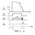
- FIG. 5 is a timing diagram 104 illustrating the operation of control circuit 100 in accordance with embodiments of the present invention.
- TRIAC dimmer 50 turns off or shuts off in response to a current I T flowing through its terminals being less than its holding current.
- the voltage at node 42 is less than reference voltage V REF2 , thus the voltage at the output of comparator 40 is at a logic low voltage level, resulting in latch 46 being in a non-latching configuration and the voltage at output 30A, i.e., the voltage at the gate of transistor 82, being at a logic low voltage level.
- pulse generator 45A generates a pulse train but it is not latched by latch 46 because latch 46 is in a non-latching configuration.
- TRIAC dimmer 50 turns on in response to receiving a trigger signal and generates a rectified TRIAC signal V RT (shown in FIG. 5 ) at input/output node 24, which results in a voltage V 42 being developed at node 42, i.e., voltage V 42 is developed at node 42 in response to applying rectified voltage signal V RT at input/output node 24.
- Voltage V 42 may be referred to as an adjusted rectified voltage because its voltage level is adjusted by voltage divider 34.
- Voltage V 42 serves as an input signal at the inverting input of comparator 32 and at the non-inverting input of comparator 40.
- comparator 40 In response to voltage V 42 exceeding reference voltage V REF2 at time t 2 , comparator 40 generates a voltage signal V TDC (shown in FIG. 5 ) having a logic high voltage level at node 42. Voltage V TDC being at a logic high voltage level causes variable reference voltage generator 102 to decrease its output voltage V REF102 to a level that is less than the voltage level at input 26 resulting in comparator 48 generating a logic high voltage level at its output that causes latch 46 to latch the pulse signal from pulse generator 45A, which pulse train appears at output 30A as voltage signal V 30A .
- the pulse train at output 30A is identified by reference character 92A in FIG. 5 and serves as an input signal to transistor 82.
- TRIAC dimmer 50 In response to rectified voltage V RT reaching the switching operation threshold voltage V SOT at time t 4 , reference voltage V REF102 decreases, which decreases switching current I SWT resulting in a lower AC current. TRIAC dimmer 50 turns off in response to the current of switching transistor 82 falling below the holding current of TRIAC dimmer 50. It should be noted that from time t 3 to time t 4 , voltage signal V 30A at the gate of switching transistor 82 continues to switch but at such a low frequency that the level of current I SWT becomes too low for TRIAC dimmer 50 to remain on. Thus, TRIAC dimmer 50 turns off. In response to voltage V RT falling to the dummy load threshold voltage level V DL (shown in FIG. 5 ) at time t 4 , comparator 32 generates a logic high voltage level at its output that turns on transistor 36, which generates a dummy load current I DL .
- FIG. 6 is a circuit schematic of a control circuit 10A suitable for controlling one or more LEDs in accordance with another embodiment of the present invention. What is shown in FIG. 6 is control circuit 10A coupled to an input circuit 12, a light generator 14, and a driver circuit 16. Control circuit 10A is similar to control circuit 10 of FIG. 1 except that a node 42 is not connected to the non-inverting input of comparator 40. Rather, input/output node 24 is connected to the non-inverting input of comparator 40 through a resistor 152. In addition, the non-inverting input of comparator 40 is connected to a source of operating potential such as, for example, V SS through a resistor 154. Resistors 152 and 154 are configured as a voltage divider network 156. Reference character "A" has been appended to reference character 10 in FIG. 6 to distinguish it from control circuit 10 of FIG. 1 .
- FIG. 7 is a circuit schematic of a control circuit 10B suitable for controlling one or more LEDs in accordance with another embodiment of the present invention. What is shown in FIG. 7 is a control circuit 10B coupled to an input circuit 12, a light generator 14, and a driver circuit 16. Control circuit 10B is similar to control circuit 10A of FIG. 6 except that a current carrying electrode of transistor 36 is coupled to input/output node 24 through a resistor 158. Reference character "B" has been appended to reference character 10 in FIG. 7 to distinguish it from control circuit 10A of FIG. 6 .
- FIG. 8 is a circuit schematic of a control circuit 100A suitable for controlling one or more LEDs in accordance with another embodiment of the present invention. What is shown in FIG. 8 is control circuit 100A coupled to an input circuit 12, a light generator 14, and a driver circuit 16. Control circuit 100A is similar to control circuit 100 of FIG. 4 except that node 42 is not connected to the non-inverting input of comparator 40. Rather, input/output node 24 is connected to the non-inverting input of comparator 40 through resistors 139 and 152. In addition, the non-inverting input of comparator 40 is connected to a source of operating potential such as, for example, V SS through resistor 154, wherein voltage V SS may be for example a ground potential. Resistors 152 and 154 are configured as a voltage divider network 156. Reference character "A" has been appended to reference character 100 in FIG. 6 to distinguish it from control circuit 100 of FIG. 4 .
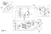
- FIG. 9 is a circuit schematic of a control circuit 100B suitable for controlling one or more light emitting diodes (LEDs) in accordance with another embodiment of the present invention. What is shown in FIG. 9 is a control circuit 100B coupled to an input circuit 12, a light generator 14, and a driver circuit 16. Control circuit 100B is similar to control circuit 100A of FIG. 8 except that a current carrying electrode of transistor 36 is coupled to input/output node 24 through a resistor 158. Reference character "B" has been appended to reference character 100 in FIG. 9 to distinguish it from control circuit 100A of FIG. 8 .
- a flicker control circuit and a method for reducing flicker have been provided.
- stable operation of an LED circuit is realized by controlling the duty cycle of a TRIAC dimmer, wherein the TRIAC dimmer is turned off at a predetermined AC voltage.
- This technique allows lower consumption of electricity by confirming the on duty of a TRIAC dimmer, which lowers the electricity used by an LED.
- Embodiments mitigates flicker by, for example, reducing a TRIAC dimmer current while maintaining stable operation of the TRIAC dimmer.
Landscapes
- Circuit Arrangement For Electric Light Sources In General (AREA)
Applications Claiming Priority (1)
| Application Number | Priority Date | Filing Date | Title |
|---|---|---|---|
| US14/098,529 US9148919B2 (en) | 2013-12-06 | 2013-12-06 | Method for mitigating flicker |
Publications (3)
| Publication Number | Publication Date |
|---|---|
| EP2882264A2 true EP2882264A2 (de) | 2015-06-10 |
| EP2882264A3 EP2882264A3 (de) | 2016-01-20 |
| EP2882264B1 EP2882264B1 (de) | 2021-04-21 |
Family
ID=52013909
Family Applications (1)
| Application Number | Title | Priority Date | Filing Date |
|---|---|---|---|
| EP14196539.2A Active EP2882264B1 (de) | 2013-12-06 | 2014-12-05 | LED Regelkreis und Verfahren |
Country Status (3)
| Country | Link |
|---|---|
| US (1) | US9148919B2 (de) |
| EP (1) | EP2882264B1 (de) |
| CN (1) | CN204697325U (de) |
Cited By (1)
| Publication number | Priority date | Publication date | Assignee | Title |
|---|---|---|---|---|
| CN110012575A (zh) * | 2019-05-09 | 2019-07-12 | 杭州必易微电子有限公司 | 驱动控制电路及控制方法 |
Families Citing this family (7)
| Publication number | Priority date | Publication date | Assignee | Title |
|---|---|---|---|---|
| KR20150002082A (ko) * | 2013-06-28 | 2015-01-07 | 주식회사 실리콘웍스 | 발광 다이오드 조명 장치 및 그의 제어 회로 |
| US9872351B2 (en) * | 2015-04-07 | 2018-01-16 | Liteideas, Llc | Device and method for encoding a signal on alternating current lines |
| WO2018209273A1 (en) * | 2017-05-11 | 2018-11-15 | ERP Power, LLC | Active preload for triac dimmers |
| US10542601B2 (en) | 2017-07-25 | 2020-01-21 | Liteideas, Llc | Smart dimming system incorporating a three-pin connector |
| CN107835543B (zh) * | 2017-11-14 | 2024-06-28 | 上海晶丰明源半导体股份有限公司 | 可控硅调光器的检测电路、芯片及方法、led驱动芯片及系统 |
| CN110300476B (zh) * | 2018-03-23 | 2022-04-12 | 台达电子工业股份有限公司 | 调光器控制电路、方法以及系统 |
| KR102138942B1 (ko) * | 2019-02-12 | 2020-07-28 | 고관수 | 트라이액 모듈 |
Citations (2)
| Publication number | Priority date | Publication date | Assignee | Title |
|---|---|---|---|---|
| US7872427B2 (en) | 2004-05-19 | 2011-01-18 | Goeken Group Corp. | Dimming circuit for LED lighting device with means for holding TRIAC in conduction |
| US8492992B2 (en) | 2009-09-18 | 2013-07-23 | Toshiba Lighting & Technology Corporation | LED lighting device and illumination apparatus |
Family Cites Families (7)
| Publication number | Priority date | Publication date | Assignee | Title |
|---|---|---|---|---|
| JP5502411B2 (ja) * | 2009-09-25 | 2014-05-28 | パナソニック株式会社 | 点灯回路およびそれを備えた光源装置 |
| US8525438B1 (en) | 2010-07-09 | 2013-09-03 | Jade Sky Technologies, Inc. | Load driver with integrated power factor correction |
| US8111017B2 (en) * | 2010-07-12 | 2012-02-07 | O2Micro, Inc | Circuits and methods for controlling dimming of a light source |
| JP5780803B2 (ja) * | 2011-03-29 | 2015-09-16 | セミコンダクター・コンポーネンツ・インダストリーズ・リミテッド・ライアビリティ・カンパニー | Led調光回路 |
| US8674605B2 (en) | 2011-05-12 | 2014-03-18 | Osram Sylvania Inc. | Driver circuit for reduced form factor solid state light source lamp |
| US8698407B1 (en) * | 2011-11-14 | 2014-04-15 | Technical Consumer Products, Inc. | Highly integrated non-inductive LED driver |
| EP2810533B1 (de) | 2012-02-02 | 2015-08-05 | Koninklijke Philips N.V. | Led-lichtquelle |
-
2013
- 2013-12-06 US US14/098,529 patent/US9148919B2/en active Active
-
2014
- 2014-12-05 EP EP14196539.2A patent/EP2882264B1/de active Active
- 2014-12-05 CN CN201420874286.1U patent/CN204697325U/zh not_active Expired - Fee Related
Patent Citations (2)
| Publication number | Priority date | Publication date | Assignee | Title |
|---|---|---|---|---|
| US7872427B2 (en) | 2004-05-19 | 2011-01-18 | Goeken Group Corp. | Dimming circuit for LED lighting device with means for holding TRIAC in conduction |
| US8492992B2 (en) | 2009-09-18 | 2013-07-23 | Toshiba Lighting & Technology Corporation | LED lighting device and illumination apparatus |
Cited By (2)
| Publication number | Priority date | Publication date | Assignee | Title |
|---|---|---|---|---|
| CN110012575A (zh) * | 2019-05-09 | 2019-07-12 | 杭州必易微电子有限公司 | 驱动控制电路及控制方法 |
| CN110012575B (zh) * | 2019-05-09 | 2024-04-19 | 杭州必易微电子有限公司 | 驱动控制电路及控制方法 |
Also Published As
| Publication number | Publication date |
|---|---|
| US9148919B2 (en) | 2015-09-29 |
| CN204697325U (zh) | 2015-10-07 |
| EP2882264B1 (de) | 2021-04-21 |
| US20150163873A1 (en) | 2015-06-11 |
| EP2882264A3 (de) | 2016-01-20 |
Similar Documents
| Publication | Publication Date | Title |
|---|---|---|
| EP2882264B1 (de) | LED Regelkreis und Verfahren | |
| US12464620B2 (en) | Systems and methods for providing power supply to current controllers associated with LED lighting | |
| US9380657B2 (en) | LED lighting device | |
| CN102057752B (zh) | 调光器触发电路、调光器系统和可调光设备 | |
| US9510407B2 (en) | LED drive circuit | |
| US9198242B2 (en) | Apparatus for driving LEDs using high voltage | |
| US8638047B2 (en) | Two-terminal current controller and related LED lighting device | |
| US8901836B2 (en) | Dimming controlling circuit for LED | |
| US11122665B1 (en) | Protective device and method of lighting assembly, lighting assembly and protective method thereof | |
| US8183798B2 (en) | Variable light control system and method using momentary circuit interrupt | |
| EP3188574A1 (de) | Beleuchtungsvorrichtung | |
| TW201715327A (zh) | 電壓控制裝置 | |
| CN106413201B (zh) | 一种用于led灯具的多种电流输出的恒流电源 | |
| JP2012530348A (ja) | トライアック調光器のためのledとの電力インターフェース | |
| US10306730B1 (en) | Light state regulation controller, control system and control method | |
| US9013109B2 (en) | Light-emitting diode lighting device with adjustable current settings and switch voltages | |
| KR101518554B1 (ko) | 다수의 led 모듈을 구동하는 전원 공급 장치와 이를 구비하는 led 조명 장치 | |
| US10440785B2 (en) | Current holding circuit for bidirectional triode thyristor dimmer and linear dimming driving circuit using the same | |
| KR102654416B1 (ko) | 발광 다이오드 조명 장치 | |
| JP2016066488A (ja) | 電源装置及び照明装置 | |
| CN103889121B (zh) | 一种纹波电流抑制电路 | |
| US8994283B2 (en) | Circuit for controlling a lighting unit having a periodic power supply with a thyristor | |
| Seo et al. | Multi-string AC-powered LED driver with current regulation reduction based on simple circuitry | |
| US20160014859A1 (en) | Led lighting apparatus | |
| EP3358911B1 (de) | Leuchtdiodensystem mit mittels stromleitungen getragenen lichtsignalen |
Legal Events
| Date | Code | Title | Description |
|---|---|---|---|
| PUAI | Public reference made under article 153(3) epc to a published international application that has entered the european phase |
Free format text: ORIGINAL CODE: 0009012 |
|
| 17P | Request for examination filed |
Effective date: 20141205 |
|
| AK | Designated contracting states |
Kind code of ref document: A2 Designated state(s): AL AT BE BG CH CY CZ DE DK EE ES FI FR GB GR HR HU IE IS IT LI LT LU LV MC MK MT NL NO PL PT RO RS SE SI SK SM TR |
|
| AX | Request for extension of the european patent |
Extension state: BA ME |
|
| RIC1 | Information provided on ipc code assigned before grant |
Ipc: H05B 33/08 20060101AFI20150710BHEP |
|
| PUAL | Search report despatched |
Free format text: ORIGINAL CODE: 0009013 |
|
| AK | Designated contracting states |
Kind code of ref document: A3 Designated state(s): AL AT BE BG CH CY CZ DE DK EE ES FI FR GB GR HR HU IE IS IT LI LT LU LV MC MK MT NL NO PL PT RO RS SE SI SK SM TR |
|
| AX | Request for extension of the european patent |
Extension state: BA ME |
|
| RIC1 | Information provided on ipc code assigned before grant |
Ipc: H05B 33/08 20060101AFI20151216BHEP |
|
| R17P | Request for examination filed (corrected) |
Effective date: 20160720 |
|
| RBV | Designated contracting states (corrected) |
Designated state(s): AL AT BE BG CH CY CZ DE DK EE ES FI FR GB GR HR HU IE IS IT LI LT LU LV MC MK MT NL NO PL PT RO RS SE SI SK SM TR |
|
| STAA | Information on the status of an ep patent application or granted ep patent |
Free format text: STATUS: EXAMINATION IS IN PROGRESS |
|
| 17Q | First examination report despatched |
Effective date: 20180816 |
|
| REG | Reference to a national code |
Ref country code: DE Ref legal event code: R079 Ref document number: 602014076741 Country of ref document: DE Free format text: PREVIOUS MAIN CLASS: H05B0033080000 Ipc: H05B0045100000 |
|
| GRAP | Despatch of communication of intention to grant a patent |
Free format text: ORIGINAL CODE: EPIDOSNIGR1 |
|
| STAA | Information on the status of an ep patent application or granted ep patent |
Free format text: STATUS: GRANT OF PATENT IS INTENDED |
|
| RIC1 | Information provided on ipc code assigned before grant |
Ipc: H05B 45/3575 20200101ALI20201022BHEP Ipc: H05B 45/3725 20200101ALI20201022BHEP Ipc: H05B 45/10 20200101AFI20201022BHEP |
|
| INTG | Intention to grant announced |
Effective date: 20201111 |
|
| GRAS | Grant fee paid |
Free format text: ORIGINAL CODE: EPIDOSNIGR3 |
|
| GRAA | (expected) grant |
Free format text: ORIGINAL CODE: 0009210 |
|
| STAA | Information on the status of an ep patent application or granted ep patent |
Free format text: STATUS: THE PATENT HAS BEEN GRANTED |
|
| AK | Designated contracting states |
Kind code of ref document: B1 Designated state(s): AL AT BE BG CH CY CZ DE DK EE ES FI FR GB GR HR HU IE IS IT LI LT LU LV MC MK MT NL NO PL PT RO RS SE SI SK SM TR |
|
| REG | Reference to a national code |
Ref country code: GB Ref legal event code: FG4D |
|
| REG | Reference to a national code |
Ref country code: CH Ref legal event code: EP |
|
| REG | Reference to a national code |
Ref country code: DE Ref legal event code: R096 Ref document number: 602014076741 Country of ref document: DE Ref country code: IE Ref legal event code: FG4D |
|
| REG | Reference to a national code |
Ref country code: AT Ref legal event code: REF Ref document number: 1386006 Country of ref document: AT Kind code of ref document: T Effective date: 20210515 |
|
| REG | Reference to a national code |
Ref country code: LT Ref legal event code: MG9D |
|
| REG | Reference to a national code |
Ref country code: AT Ref legal event code: MK05 Ref document number: 1386006 Country of ref document: AT Kind code of ref document: T Effective date: 20210421 |
|
| REG | Reference to a national code |
Ref country code: NL Ref legal event code: MP Effective date: 20210421 |
|
| PG25 | Lapsed in a contracting state [announced via postgrant information from national office to epo] |
Ref country code: BG Free format text: LAPSE BECAUSE OF FAILURE TO SUBMIT A TRANSLATION OF THE DESCRIPTION OR TO PAY THE FEE WITHIN THE PRESCRIBED TIME-LIMIT Effective date: 20210721 Ref country code: AT Free format text: LAPSE BECAUSE OF FAILURE TO SUBMIT A TRANSLATION OF THE DESCRIPTION OR TO PAY THE FEE WITHIN THE PRESCRIBED TIME-LIMIT Effective date: 20210421 Ref country code: FI Free format text: LAPSE BECAUSE OF FAILURE TO SUBMIT A TRANSLATION OF THE DESCRIPTION OR TO PAY THE FEE WITHIN THE PRESCRIBED TIME-LIMIT Effective date: 20210421 Ref country code: NL Free format text: LAPSE BECAUSE OF FAILURE TO SUBMIT A TRANSLATION OF THE DESCRIPTION OR TO PAY THE FEE WITHIN THE PRESCRIBED TIME-LIMIT Effective date: 20210421 Ref country code: LT Free format text: LAPSE BECAUSE OF FAILURE TO SUBMIT A TRANSLATION OF THE DESCRIPTION OR TO PAY THE FEE WITHIN THE PRESCRIBED TIME-LIMIT Effective date: 20210421 Ref country code: HR Free format text: LAPSE BECAUSE OF FAILURE TO SUBMIT A TRANSLATION OF THE DESCRIPTION OR TO PAY THE FEE WITHIN THE PRESCRIBED TIME-LIMIT Effective date: 20210421 |
|
| PG25 | Lapsed in a contracting state [announced via postgrant information from national office to epo] |
Ref country code: GR Free format text: LAPSE BECAUSE OF FAILURE TO SUBMIT A TRANSLATION OF THE DESCRIPTION OR TO PAY THE FEE WITHIN THE PRESCRIBED TIME-LIMIT Effective date: 20210722 Ref country code: LV Free format text: LAPSE BECAUSE OF FAILURE TO SUBMIT A TRANSLATION OF THE DESCRIPTION OR TO PAY THE FEE WITHIN THE PRESCRIBED TIME-LIMIT Effective date: 20210421 Ref country code: IS Free format text: LAPSE BECAUSE OF FAILURE TO SUBMIT A TRANSLATION OF THE DESCRIPTION OR TO PAY THE FEE WITHIN THE PRESCRIBED TIME-LIMIT Effective date: 20210821 Ref country code: SE Free format text: LAPSE BECAUSE OF FAILURE TO SUBMIT A TRANSLATION OF THE DESCRIPTION OR TO PAY THE FEE WITHIN THE PRESCRIBED TIME-LIMIT Effective date: 20210421 Ref country code: RS Free format text: LAPSE BECAUSE OF FAILURE TO SUBMIT A TRANSLATION OF THE DESCRIPTION OR TO PAY THE FEE WITHIN THE PRESCRIBED TIME-LIMIT Effective date: 20210421 Ref country code: PL Free format text: LAPSE BECAUSE OF FAILURE TO SUBMIT A TRANSLATION OF THE DESCRIPTION OR TO PAY THE FEE WITHIN THE PRESCRIBED TIME-LIMIT Effective date: 20210421 Ref country code: NO Free format text: LAPSE BECAUSE OF FAILURE TO SUBMIT A TRANSLATION OF THE DESCRIPTION OR TO PAY THE FEE WITHIN THE PRESCRIBED TIME-LIMIT Effective date: 20210721 Ref country code: PT Free format text: LAPSE BECAUSE OF FAILURE TO SUBMIT A TRANSLATION OF THE DESCRIPTION OR TO PAY THE FEE WITHIN THE PRESCRIBED TIME-LIMIT Effective date: 20210823 Ref country code: ES Free format text: LAPSE BECAUSE OF FAILURE TO SUBMIT A TRANSLATION OF THE DESCRIPTION OR TO PAY THE FEE WITHIN THE PRESCRIBED TIME-LIMIT Effective date: 20210421 |
|
| REG | Reference to a national code |
Ref country code: DE Ref legal event code: R097 Ref document number: 602014076741 Country of ref document: DE |
|
| PG25 | Lapsed in a contracting state [announced via postgrant information from national office to epo] |
Ref country code: SK Free format text: LAPSE BECAUSE OF FAILURE TO SUBMIT A TRANSLATION OF THE DESCRIPTION OR TO PAY THE FEE WITHIN THE PRESCRIBED TIME-LIMIT Effective date: 20210421 Ref country code: SM Free format text: LAPSE BECAUSE OF FAILURE TO SUBMIT A TRANSLATION OF THE DESCRIPTION OR TO PAY THE FEE WITHIN THE PRESCRIBED TIME-LIMIT Effective date: 20210421 Ref country code: DK Free format text: LAPSE BECAUSE OF FAILURE TO SUBMIT A TRANSLATION OF THE DESCRIPTION OR TO PAY THE FEE WITHIN THE PRESCRIBED TIME-LIMIT Effective date: 20210421 Ref country code: EE Free format text: LAPSE BECAUSE OF FAILURE TO SUBMIT A TRANSLATION OF THE DESCRIPTION OR TO PAY THE FEE WITHIN THE PRESCRIBED TIME-LIMIT Effective date: 20210421 Ref country code: CZ Free format text: LAPSE BECAUSE OF FAILURE TO SUBMIT A TRANSLATION OF THE DESCRIPTION OR TO PAY THE FEE WITHIN THE PRESCRIBED TIME-LIMIT Effective date: 20210421 Ref country code: RO Free format text: LAPSE BECAUSE OF FAILURE TO SUBMIT A TRANSLATION OF THE DESCRIPTION OR TO PAY THE FEE WITHIN THE PRESCRIBED TIME-LIMIT Effective date: 20210421 |
|
| PLBE | No opposition filed within time limit |
Free format text: ORIGINAL CODE: 0009261 |
|
| STAA | Information on the status of an ep patent application or granted ep patent |
Free format text: STATUS: NO OPPOSITION FILED WITHIN TIME LIMIT |
|
| 26N | No opposition filed |
Effective date: 20220124 |
|
| PG25 | Lapsed in a contracting state [announced via postgrant information from national office to epo] |
Ref country code: IS Free format text: LAPSE BECAUSE OF FAILURE TO SUBMIT A TRANSLATION OF THE DESCRIPTION OR TO PAY THE FEE WITHIN THE PRESCRIBED TIME-LIMIT Effective date: 20210821 Ref country code: AL Free format text: LAPSE BECAUSE OF FAILURE TO SUBMIT A TRANSLATION OF THE DESCRIPTION OR TO PAY THE FEE WITHIN THE PRESCRIBED TIME-LIMIT Effective date: 20210421 |
|
| REG | Reference to a national code |
Ref country code: DE Ref legal event code: R119 Ref document number: 602014076741 Country of ref document: DE |
|
| PG25 | Lapsed in a contracting state [announced via postgrant information from national office to epo] |
Ref country code: MC Free format text: LAPSE BECAUSE OF FAILURE TO SUBMIT A TRANSLATION OF THE DESCRIPTION OR TO PAY THE FEE WITHIN THE PRESCRIBED TIME-LIMIT Effective date: 20210421 Ref country code: IT Free format text: LAPSE BECAUSE OF FAILURE TO SUBMIT A TRANSLATION OF THE DESCRIPTION OR TO PAY THE FEE WITHIN THE PRESCRIBED TIME-LIMIT Effective date: 20210421 |
|
| REG | Reference to a national code |
Ref country code: CH Ref legal event code: PL |
|
| GBPC | Gb: european patent ceased through non-payment of renewal fee |
Effective date: 20211205 |
|
| REG | Reference to a national code |
Ref country code: BE Ref legal event code: MM Effective date: 20211231 |
|
| PG25 | Lapsed in a contracting state [announced via postgrant information from national office to epo] |
Ref country code: LU Free format text: LAPSE BECAUSE OF NON-PAYMENT OF DUE FEES Effective date: 20211205 Ref country code: IE Free format text: LAPSE BECAUSE OF NON-PAYMENT OF DUE FEES Effective date: 20211205 Ref country code: GB Free format text: LAPSE BECAUSE OF NON-PAYMENT OF DUE FEES Effective date: 20211205 Ref country code: DE Free format text: LAPSE BECAUSE OF NON-PAYMENT OF DUE FEES Effective date: 20220701 |
|
| PG25 | Lapsed in a contracting state [announced via postgrant information from national office to epo] |
Ref country code: BE Free format text: LAPSE BECAUSE OF NON-PAYMENT OF DUE FEES Effective date: 20211231 |
|
| PG25 | Lapsed in a contracting state [announced via postgrant information from national office to epo] |
Ref country code: LI Free format text: LAPSE BECAUSE OF NON-PAYMENT OF DUE FEES Effective date: 20211231 Ref country code: CH Free format text: LAPSE BECAUSE OF NON-PAYMENT OF DUE FEES Effective date: 20211231 |
|
| PGFP | Annual fee paid to national office [announced via postgrant information from national office to epo] |
Ref country code: FR Payment date: 20221122 Year of fee payment: 9 |
|
| PG25 | Lapsed in a contracting state [announced via postgrant information from national office to epo] |
Ref country code: HU Free format text: LAPSE BECAUSE OF FAILURE TO SUBMIT A TRANSLATION OF THE DESCRIPTION OR TO PAY THE FEE WITHIN THE PRESCRIBED TIME-LIMIT; INVALID AB INITIO Effective date: 20141205 |
|
| P01 | Opt-out of the competence of the unified patent court (upc) registered |
Effective date: 20230519 |
|
| PG25 | Lapsed in a contracting state [announced via postgrant information from national office to epo] |
Ref country code: CY Free format text: LAPSE BECAUSE OF FAILURE TO SUBMIT A TRANSLATION OF THE DESCRIPTION OR TO PAY THE FEE WITHIN THE PRESCRIBED TIME-LIMIT Effective date: 20210421 |
|
| PG25 | Lapsed in a contracting state [announced via postgrant information from national office to epo] |
Ref country code: MK Free format text: LAPSE BECAUSE OF FAILURE TO SUBMIT A TRANSLATION OF THE DESCRIPTION OR TO PAY THE FEE WITHIN THE PRESCRIBED TIME-LIMIT Effective date: 20210421 |
|
| PG25 | Lapsed in a contracting state [announced via postgrant information from national office to epo] |
Ref country code: TR Free format text: LAPSE BECAUSE OF FAILURE TO SUBMIT A TRANSLATION OF THE DESCRIPTION OR TO PAY THE FEE WITHIN THE PRESCRIBED TIME-LIMIT Effective date: 20210421 |
|
| PG25 | Lapsed in a contracting state [announced via postgrant information from national office to epo] |
Ref country code: MT Free format text: LAPSE BECAUSE OF FAILURE TO SUBMIT A TRANSLATION OF THE DESCRIPTION OR TO PAY THE FEE WITHIN THE PRESCRIBED TIME-LIMIT Effective date: 20210421 |
|
| PG25 | Lapsed in a contracting state [announced via postgrant information from national office to epo] |
Ref country code: FR Free format text: LAPSE BECAUSE OF NON-PAYMENT OF DUE FEES Effective date: 20231231 |
|
| PG25 | Lapsed in a contracting state [announced via postgrant information from national office to epo] |
Ref country code: FR Free format text: LAPSE BECAUSE OF NON-PAYMENT OF DUE FEES Effective date: 20231231 |