EP2882005A1 - Electronic device - Google Patents
Electronic device Download PDFInfo
- Publication number
- EP2882005A1 EP2882005A1 EP14194525.3A EP14194525A EP2882005A1 EP 2882005 A1 EP2882005 A1 EP 2882005A1 EP 14194525 A EP14194525 A EP 14194525A EP 2882005 A1 EP2882005 A1 EP 2882005A1
- Authority
- EP
- European Patent Office
- Prior art keywords
- substituted
- alkyl
- photo
- group
- formula
- Prior art date
- Legal status (The legal status is an assumption and is not a legal conclusion. Google has not performed a legal analysis and makes no representation as to the accuracy of the status listed.)
- Withdrawn
Links
- 239000004065 semiconductor Substances 0.000 claims abstract description 82
- 229920000642 polymer Polymers 0.000 claims abstract description 77
- 150000001875 compounds Chemical class 0.000 claims abstract description 73
- 239000000758 substrate Substances 0.000 claims abstract description 37
- 125000001072 heteroaryl group Chemical group 0.000 claims description 45
- 125000000217 alkyl group Chemical group 0.000 claims description 42
- 229910052736 halogen Inorganic materials 0.000 claims description 31
- 150000002367 halogens Chemical class 0.000 claims description 31
- 125000003118 aryl group Chemical group 0.000 claims description 28
- 125000000547 substituted alkyl group Chemical group 0.000 claims description 27
- 125000003545 alkoxy group Chemical group 0.000 claims description 26
- -1 trialkylsilylalkynyl Chemical group 0.000 claims description 25
- 125000003342 alkenyl group Chemical group 0.000 claims description 24
- 125000004093 cyano group Chemical group *C#N 0.000 claims description 24
- 125000005017 substituted alkenyl group Chemical group 0.000 claims description 23
- 125000004414 alkyl thio group Chemical group 0.000 claims description 22
- 125000000304 alkynyl group Chemical group 0.000 claims description 22
- 125000004665 trialkylsilyl group Chemical group 0.000 claims description 22
- 125000004426 substituted alkynyl group Chemical group 0.000 claims description 21
- 125000003107 substituted aryl group Chemical group 0.000 claims description 20
- DMLAVOWQYNRWNQ-UHFFFAOYSA-N azobenzene Chemical group C1=CC=CC=C1N=NC1=CC=CC=C1 DMLAVOWQYNRWNQ-UHFFFAOYSA-N 0.000 claims description 16
- 229910052717 sulfur Inorganic materials 0.000 claims description 15
- PJANXHGTPQOBST-UHFFFAOYSA-N stilbene Chemical group C=1C=CC=CC=1C=CC1=CC=CC=C1 PJANXHGTPQOBST-UHFFFAOYSA-N 0.000 claims description 7
- 229910052760 oxygen Inorganic materials 0.000 claims description 6
- 125000001997 phenyl group Chemical group [H]C1=C([H])C([H])=C(*)C([H])=C1[H] 0.000 claims description 6
- WBYWAXJHAXSJNI-VOTSOKGWSA-M trans-cinnamate Chemical group [O-]C(=O)\C=C\C1=CC=CC=C1 WBYWAXJHAXSJNI-VOTSOKGWSA-M 0.000 claims description 6
- 125000000332 coumarinyl group Chemical group O1C(=O)C(=CC2=CC=CC=C12)* 0.000 claims description 4
- 125000001624 naphthyl group Chemical group 0.000 claims description 4
- 229910052711 selenium Inorganic materials 0.000 claims description 4
- 125000001706 diarylethene group Chemical group 0.000 claims description 3
- 150000004753 Schiff bases Chemical group 0.000 claims description 2
- 125000002485 formyl group Chemical class [H]C(*)=O 0.000 claims 6
- 239000010410 layer Substances 0.000 description 102
- 150000001299 aldehydes Chemical class 0.000 description 19
- 239000000463 material Substances 0.000 description 18
- 125000004435 hydrogen atom Chemical group [H]* 0.000 description 17
- 229910052739 hydrogen Inorganic materials 0.000 description 16
- 239000001257 hydrogen Substances 0.000 description 16
- 238000000034 method Methods 0.000 description 15
- 125000004432 carbon atom Chemical group C* 0.000 description 13
- 239000000178 monomer Substances 0.000 description 13
- 229920001577 copolymer Polymers 0.000 description 11
- 125000000449 nitro group Chemical group [O-][N+](*)=O 0.000 description 10
- 229920003229 poly(methyl methacrylate) Polymers 0.000 description 10
- 239000004926 polymethyl methacrylate Substances 0.000 description 10
- 125000002887 hydroxy group Chemical group [H]O* 0.000 description 9
- 125000002924 primary amino group Chemical group [H]N([H])* 0.000 description 9
- XUIMIQQOPSSXEZ-UHFFFAOYSA-N Silicon Chemical compound [Si] XUIMIQQOPSSXEZ-UHFFFAOYSA-N 0.000 description 8
- NINIDFKCEFEMDL-UHFFFAOYSA-N Sulfur Chemical group [S] NINIDFKCEFEMDL-UHFFFAOYSA-N 0.000 description 8
- 238000004770 highest occupied molecular orbital Methods 0.000 description 8
- 230000014759 maintenance of location Effects 0.000 description 8
- 229910052710 silicon Inorganic materials 0.000 description 8
- 239000011593 sulfur Substances 0.000 description 8
- 150000003573 thiols Chemical class 0.000 description 8
- UFHFLCQGNIYNRP-UHFFFAOYSA-N Hydrogen Chemical compound [H][H] UFHFLCQGNIYNRP-UHFFFAOYSA-N 0.000 description 7
- 239000010408 film Substances 0.000 description 7
- WYURNTSHIVDZCO-UHFFFAOYSA-N Tetrahydrofuran Chemical compound C1CCOC1 WYURNTSHIVDZCO-UHFFFAOYSA-N 0.000 description 6
- 238000010276 construction Methods 0.000 description 6
- 238000005286 illumination Methods 0.000 description 6
- 230000001678 irradiating effect Effects 0.000 description 6
- 230000008569 process Effects 0.000 description 6
- 239000010703 silicon Substances 0.000 description 6
- 238000006243 chemical reaction Methods 0.000 description 5
- 229920001940 conductive polymer Polymers 0.000 description 5
- IJGRMHOSHXDMSA-UHFFFAOYSA-N Atomic nitrogen Chemical compound N#N IJGRMHOSHXDMSA-UHFFFAOYSA-N 0.000 description 4
- FOQABOMYTOFLPZ-ISLYRVAYSA-N Disperse Red 1 Chemical compound C1=CC(N(CCO)CC)=CC=C1\N=N\C1=CC=C([N+]([O-])=O)C=C1 FOQABOMYTOFLPZ-ISLYRVAYSA-N 0.000 description 4
- KDLHZDBZIXYQEI-UHFFFAOYSA-N Palladium Chemical compound [Pd] KDLHZDBZIXYQEI-UHFFFAOYSA-N 0.000 description 4
- 239000004793 Polystyrene Substances 0.000 description 4
- MVPPADPHJFYWMZ-UHFFFAOYSA-N chlorobenzene Chemical compound ClC1=CC=CC=C1 MVPPADPHJFYWMZ-UHFFFAOYSA-N 0.000 description 4
- 238000010586 diagram Methods 0.000 description 4
- UAOMVDZJSHZZME-UHFFFAOYSA-N diisopropylamine Chemical compound CC(C)NC(C)C UAOMVDZJSHZZME-UHFFFAOYSA-N 0.000 description 4
- 230000000694 effects Effects 0.000 description 4
- 239000007772 electrode material Substances 0.000 description 4
- PCHJSUWPFVWCPO-UHFFFAOYSA-N gold Chemical compound [Au] PCHJSUWPFVWCPO-UHFFFAOYSA-N 0.000 description 4
- 229910052737 gold Inorganic materials 0.000 description 4
- 239000010931 gold Substances 0.000 description 4
- FFUAGWLWBBFQJT-UHFFFAOYSA-N hexamethyldisilazane Chemical compound C[Si](C)(C)N[Si](C)(C)C FFUAGWLWBBFQJT-UHFFFAOYSA-N 0.000 description 4
- 239000000976 ink Substances 0.000 description 4
- 229910052757 nitrogen Inorganic materials 0.000 description 4
- 229920002223 polystyrene Polymers 0.000 description 4
- 239000002904 solvent Substances 0.000 description 4
- 238000004528 spin coating Methods 0.000 description 4
- 239000010409 thin film Substances 0.000 description 4
- ZWEHNKRNPOVVGH-UHFFFAOYSA-N 2-Butanone Chemical compound CCC(C)=O ZWEHNKRNPOVVGH-UHFFFAOYSA-N 0.000 description 3
- XFXPMWWXUTWYJX-UHFFFAOYSA-N Cyanide Chemical compound N#[C-] XFXPMWWXUTWYJX-UHFFFAOYSA-N 0.000 description 3
- KWYUFKZDYYNOTN-UHFFFAOYSA-M Potassium hydroxide Chemical compound [OH-].[K+] KWYUFKZDYYNOTN-UHFFFAOYSA-M 0.000 description 3
- 239000002262 Schiff base Substances 0.000 description 3
- VYPSYNLAJGMNEJ-UHFFFAOYSA-N Silicium dioxide Chemical compound O=[Si]=O VYPSYNLAJGMNEJ-UHFFFAOYSA-N 0.000 description 3
- BQCADISMDOOEFD-UHFFFAOYSA-N Silver Chemical compound [Ag] BQCADISMDOOEFD-UHFFFAOYSA-N 0.000 description 3
- PJANXHGTPQOBST-VAWYXSNFSA-N Stilbene Natural products C=1C=CC=CC=1/C=C/C1=CC=CC=C1 PJANXHGTPQOBST-VAWYXSNFSA-N 0.000 description 3
- YXFVVABEGXRONW-UHFFFAOYSA-N Toluene Chemical compound CC1=CC=CC=C1 YXFVVABEGXRONW-UHFFFAOYSA-N 0.000 description 3
- 150000001345 alkine derivatives Chemical class 0.000 description 3
- 229910052782 aluminium Inorganic materials 0.000 description 3
- XAGFODPZIPBFFR-UHFFFAOYSA-N aluminium Chemical compound [Al] XAGFODPZIPBFFR-UHFFFAOYSA-N 0.000 description 3
- 230000006399 behavior Effects 0.000 description 3
- 125000003178 carboxy group Chemical group [H]OC(*)=O 0.000 description 3
- 239000000460 chlorine Substances 0.000 description 3
- 229940114081 cinnamate Drugs 0.000 description 3
- 238000007697 cis-trans-isomerization reaction Methods 0.000 description 3
- 239000002322 conducting polymer Substances 0.000 description 3
- 238000000151 deposition Methods 0.000 description 3
- MTHSVFCYNBDYFN-UHFFFAOYSA-N diethylene glycol Chemical compound OCCOCCO MTHSVFCYNBDYFN-UHFFFAOYSA-N 0.000 description 3
- 125000005842 heteroatom Chemical group 0.000 description 3
- 229920002521 macromolecule Polymers 0.000 description 3
- 230000003446 memory effect Effects 0.000 description 3
- 229910052751 metal Inorganic materials 0.000 description 3
- 239000002184 metal Substances 0.000 description 3
- 239000000203 mixture Substances 0.000 description 3
- 239000003607 modifier Substances 0.000 description 3
- VLKZOEOYAKHREP-UHFFFAOYSA-N n-Hexane Chemical compound CCCCCC VLKZOEOYAKHREP-UHFFFAOYSA-N 0.000 description 3
- 238000007639 printing Methods 0.000 description 3
- 229910052814 silicon oxide Inorganic materials 0.000 description 3
- 229910052709 silver Inorganic materials 0.000 description 3
- 239000004332 silver Substances 0.000 description 3
- 235000021286 stilbenes Nutrition 0.000 description 3
- 238000009281 ultraviolet germicidal irradiation Methods 0.000 description 3
- FYGHSUNMUKGBRK-UHFFFAOYSA-N 1,2,3-trimethylbenzene Chemical compound CC1=CC=CC(C)=C1C FYGHSUNMUKGBRK-UHFFFAOYSA-N 0.000 description 2
- MHYWMAUCJNDHPY-UHFFFAOYSA-N 2-[n-ethyl-4-[(4-nitrophenyl)diazenyl]anilino]ethyl 2-methylprop-2-enoate Chemical compound C1=CC(N(CCOC(=O)C(C)=C)CC)=CC=C1N=NC1=CC=C([N+]([O-])=O)C=C1 MHYWMAUCJNDHPY-UHFFFAOYSA-N 0.000 description 2
- GOLORTLGFDVFDW-UHFFFAOYSA-N 3-(1h-benzimidazol-2-yl)-7-(diethylamino)chromen-2-one Chemical compound C1=CC=C2NC(C3=CC4=CC=C(C=C4OC3=O)N(CC)CC)=NC2=C1 GOLORTLGFDVFDW-UHFFFAOYSA-N 0.000 description 2
- CSCPPACGZOOCGX-UHFFFAOYSA-N Acetone Chemical compound CC(C)=O CSCPPACGZOOCGX-UHFFFAOYSA-N 0.000 description 2
- NIXOWILDQLNWCW-UHFFFAOYSA-M Acrylate Chemical compound [O-]C(=O)C=C NIXOWILDQLNWCW-UHFFFAOYSA-M 0.000 description 2
- WKBOTKDWSSQWDR-UHFFFAOYSA-N Bromine atom Chemical compound [Br] WKBOTKDWSSQWDR-UHFFFAOYSA-N 0.000 description 2
- ZAMOUSCENKQFHK-UHFFFAOYSA-N Chlorine atom Chemical compound [Cl] ZAMOUSCENKQFHK-UHFFFAOYSA-N 0.000 description 2
- HEDRZPFGACZZDS-UHFFFAOYSA-N Chloroform Chemical compound ClC(Cl)Cl HEDRZPFGACZZDS-UHFFFAOYSA-N 0.000 description 2
- VYZAMTAEIAYCRO-UHFFFAOYSA-N Chromium Chemical compound [Cr] VYZAMTAEIAYCRO-UHFFFAOYSA-N 0.000 description 2
- YNQLUTRBYVCPMQ-UHFFFAOYSA-N Ethylbenzene Chemical compound CCC1=CC=CC=C1 YNQLUTRBYVCPMQ-UHFFFAOYSA-N 0.000 description 2
- PXGOKWXKJXAPGV-UHFFFAOYSA-N Fluorine Chemical compound FF PXGOKWXKJXAPGV-UHFFFAOYSA-N 0.000 description 2
- OAKJQQAXSVQMHS-UHFFFAOYSA-N Hydrazine Chemical compound NN OAKJQQAXSVQMHS-UHFFFAOYSA-N 0.000 description 2
- BAPJBEWLBFYGME-UHFFFAOYSA-N Methyl acrylate Chemical compound COC(=O)C=C BAPJBEWLBFYGME-UHFFFAOYSA-N 0.000 description 2
- VVQNEPGJFQJSBK-UHFFFAOYSA-N Methyl methacrylate Chemical compound COC(=O)C(C)=C VVQNEPGJFQJSBK-UHFFFAOYSA-N 0.000 description 2
- LRHPLDYGYMQRHN-UHFFFAOYSA-N N-Butanol Chemical compound CCCCO LRHPLDYGYMQRHN-UHFFFAOYSA-N 0.000 description 2
- IMNFDUFMRHMDMM-UHFFFAOYSA-N N-Heptane Chemical compound CCCCCCC IMNFDUFMRHMDMM-UHFFFAOYSA-N 0.000 description 2
- PXHVJJICTQNCMI-UHFFFAOYSA-N Nickel Chemical compound [Ni] PXHVJJICTQNCMI-UHFFFAOYSA-N 0.000 description 2
- 229920001609 Poly(3,4-ethylenedioxythiophene) Polymers 0.000 description 2
- 239000004642 Polyimide Substances 0.000 description 2
- NXCSDJOTXUWERI-UHFFFAOYSA-N [1]benzothiolo[3,2-b][1]benzothiole Chemical group C12=CC=CC=C2SC2=C1SC1=CC=CC=C21 NXCSDJOTXUWERI-UHFFFAOYSA-N 0.000 description 2
- 230000000903 blocking effect Effects 0.000 description 2
- GDTBXPJZTBHREO-UHFFFAOYSA-N bromine Substances BrBr GDTBXPJZTBHREO-UHFFFAOYSA-N 0.000 description 2
- 229910052794 bromium Inorganic materials 0.000 description 2
- 239000011203 carbon fibre reinforced carbon Substances 0.000 description 2
- 230000008859 change Effects 0.000 description 2
- 239000002800 charge carrier Substances 0.000 description 2
- 229910052801 chlorine Inorganic materials 0.000 description 2
- 229910052804 chromium Inorganic materials 0.000 description 2
- 239000011651 chromium Substances 0.000 description 2
- 239000011248 coating agent Substances 0.000 description 2
- 238000000576 coating method Methods 0.000 description 2
- ZYGHJZDHTFUPRJ-UHFFFAOYSA-N coumarin Chemical compound C1=CC=C2OC(=O)C=CC2=C1 ZYGHJZDHTFUPRJ-UHFFFAOYSA-N 0.000 description 2
- 125000004122 cyclic group Chemical group 0.000 description 2
- NNBZCPXTIHJBJL-UHFFFAOYSA-N decalin Chemical compound C1CCCC2CCCCC21 NNBZCPXTIHJBJL-UHFFFAOYSA-N 0.000 description 2
- 150000001988 diarylethenes Chemical class 0.000 description 2
- 238000002474 experimental method Methods 0.000 description 2
- 239000011737 fluorine Substances 0.000 description 2
- 229910052731 fluorine Inorganic materials 0.000 description 2
- 230000006870 function Effects 0.000 description 2
- 125000000524 functional group Chemical group 0.000 description 2
- 238000005227 gel permeation chromatography Methods 0.000 description 2
- 239000011521 glass Substances 0.000 description 2
- ZSIAUFGUXNUGDI-UHFFFAOYSA-N hexan-1-ol Chemical compound CCCCCCO ZSIAUFGUXNUGDI-UHFFFAOYSA-N 0.000 description 2
- AMGQUBHHOARCQH-UHFFFAOYSA-N indium;oxotin Chemical compound [In].[Sn]=O AMGQUBHHOARCQH-UHFFFAOYSA-N 0.000 description 2
- 238000007641 inkjet printing Methods 0.000 description 2
- 229910010272 inorganic material Inorganic materials 0.000 description 2
- 239000011147 inorganic material Substances 0.000 description 2
- 238000004519 manufacturing process Methods 0.000 description 2
- 238000005259 measurement Methods 0.000 description 2
- 229910044991 metal oxide Inorganic materials 0.000 description 2
- 150000004706 metal oxides Chemical class 0.000 description 2
- 230000004048 modification Effects 0.000 description 2
- 238000012986 modification Methods 0.000 description 2
- QJGQUHMNIGDVPM-UHFFFAOYSA-N nitrogen group Chemical group [N] QJGQUHMNIGDVPM-UHFFFAOYSA-N 0.000 description 2
- 230000003287 optical effect Effects 0.000 description 2
- 229920000620 organic polymer Polymers 0.000 description 2
- 229920003023 plastic Polymers 0.000 description 2
- 239000004033 plastic Substances 0.000 description 2
- 239000002985 plastic film Substances 0.000 description 2
- BASFCYQUMIYNBI-UHFFFAOYSA-N platinum Chemical compound [Pt] BASFCYQUMIYNBI-UHFFFAOYSA-N 0.000 description 2
- 229920000515 polycarbonate Polymers 0.000 description 2
- 239000004417 polycarbonate Substances 0.000 description 2
- 229920000728 polyester Polymers 0.000 description 2
- 229920001721 polyimide Polymers 0.000 description 2
- 229920005596 polymer binder Polymers 0.000 description 2
- 239000002491 polymer binding agent Substances 0.000 description 2
- 239000002952 polymeric resin Substances 0.000 description 2
- 125000006239 protecting group Chemical group 0.000 description 2
- 230000002441 reversible effect Effects 0.000 description 2
- 238000007650 screen-printing Methods 0.000 description 2
- 125000001424 substituent group Chemical group 0.000 description 2
- 125000000472 sulfonyl group Chemical group *S(*)(=O)=O 0.000 description 2
- 238000010408 sweeping Methods 0.000 description 2
- 229920003002 synthetic resin Polymers 0.000 description 2
- 238000012360 testing method Methods 0.000 description 2
- YLQBMQCUIZJEEH-UHFFFAOYSA-N tetrahydrofuran Natural products C=1C=COC=1 YLQBMQCUIZJEEH-UHFFFAOYSA-N 0.000 description 2
- 125000003944 tolyl group Chemical group 0.000 description 2
- RIOQSEWOXXDEQQ-UHFFFAOYSA-N triphenylphosphine Chemical compound C1=CC=CC=C1P(C=1C=CC=CC=1)C1=CC=CC=C1 RIOQSEWOXXDEQQ-UHFFFAOYSA-N 0.000 description 2
- 125000000391 vinyl group Chemical group [H]C([*])=C([H])[H] 0.000 description 2
- SCYULBFZEHDVBN-UHFFFAOYSA-N 1,1-Dichloroethane Chemical compound CC(Cl)Cl SCYULBFZEHDVBN-UHFFFAOYSA-N 0.000 description 1
- RELMFMZEBKVZJC-UHFFFAOYSA-N 1,2,3-trichlorobenzene Chemical compound ClC1=CC=CC(Cl)=C1Cl RELMFMZEBKVZJC-UHFFFAOYSA-N 0.000 description 1
- OCJBOOLMMGQPQU-UHFFFAOYSA-N 1,4-dichlorobenzene Chemical compound ClC1=CC=C(Cl)C=C1 OCJBOOLMMGQPQU-UHFFFAOYSA-N 0.000 description 1
- NGNBDVOYPDDBFK-UHFFFAOYSA-N 2-[2,4-di(pentan-2-yl)phenoxy]acetyl chloride Chemical compound CCCC(C)C1=CC=C(OCC(Cl)=O)C(C(C)CCC)=C1 NGNBDVOYPDDBFK-UHFFFAOYSA-N 0.000 description 1
- ZCYVEMRRCGMTRW-UHFFFAOYSA-N 7553-56-2 Chemical compound [I] ZCYVEMRRCGMTRW-UHFFFAOYSA-N 0.000 description 1
- QGZKDVFQNNGYKY-UHFFFAOYSA-O Ammonium Chemical compound [NH4+] QGZKDVFQNNGYKY-UHFFFAOYSA-O 0.000 description 1
- OKTJSMMVPCPJKN-UHFFFAOYSA-N Carbon Chemical compound [C] OKTJSMMVPCPJKN-UHFFFAOYSA-N 0.000 description 1
- ZNZYKNKBJPZETN-WELNAUFTSA-N Dialdehyde 11678 Chemical compound N1C2=CC=CC=C2C2=C1[C@H](C[C@H](/C(=C/O)C(=O)OC)[C@@H](C=C)C=O)NCC2 ZNZYKNKBJPZETN-WELNAUFTSA-N 0.000 description 1
- CTQNGGLPUBDAKN-UHFFFAOYSA-N O-Xylene Chemical compound CC1=CC=CC=C1C CTQNGGLPUBDAKN-UHFFFAOYSA-N 0.000 description 1
- 229920001167 Poly(triaryl amine) Polymers 0.000 description 1
- 229910006069 SO3H Inorganic materials 0.000 description 1
- 229910052581 Si3N4 Inorganic materials 0.000 description 1
- RTAQQCXQSZGOHL-UHFFFAOYSA-N Titanium Chemical compound [Ti] RTAQQCXQSZGOHL-UHFFFAOYSA-N 0.000 description 1
- 238000005644 Wolff-Kishner reduction reaction Methods 0.000 description 1
- HCHKCACWOHOZIP-UHFFFAOYSA-N Zinc Chemical compound [Zn] HCHKCACWOHOZIP-UHFFFAOYSA-N 0.000 description 1
- RCAQADNJXBGEKC-UHFFFAOYSA-N [O].[In].[Sb] Chemical compound [O].[In].[Sb] RCAQADNJXBGEKC-UHFFFAOYSA-N 0.000 description 1
- 238000002835 absorbance Methods 0.000 description 1
- 150000001242 acetic acid derivatives Chemical class 0.000 description 1
- 150000001252 acrylic acid derivatives Chemical class 0.000 description 1
- 150000001298 alcohols Chemical class 0.000 description 1
- VSCWAEJMTAWNJL-UHFFFAOYSA-K aluminium trichloride Chemical compound Cl[Al](Cl)Cl VSCWAEJMTAWNJL-UHFFFAOYSA-K 0.000 description 1
- MDFFNEOEWAXZRQ-UHFFFAOYSA-N aminyl Chemical compound [NH2] MDFFNEOEWAXZRQ-UHFFFAOYSA-N 0.000 description 1
- 238000000137 annealing Methods 0.000 description 1
- 150000004945 aromatic hydrocarbons Chemical class 0.000 description 1
- 125000004429 atom Chemical group 0.000 description 1
- JRPBQTZRNDNNOP-UHFFFAOYSA-N barium titanate Chemical compound [Ba+2].[Ba+2].[O-][Ti]([O-])([O-])[O-] JRPBQTZRNDNNOP-UHFFFAOYSA-N 0.000 description 1
- 229910002113 barium titanate Inorganic materials 0.000 description 1
- YIMPFANPVKETMG-UHFFFAOYSA-N barium zirconium Chemical compound [Zr].[Ba] YIMPFANPVKETMG-UHFFFAOYSA-N 0.000 description 1
- 239000002585 base Substances 0.000 description 1
- 230000008901 benefit Effects 0.000 description 1
- KCXMKQUNVWSEMD-UHFFFAOYSA-N benzyl chloride Chemical compound ClCC1=CC=CC=C1 KCXMKQUNVWSEMD-UHFFFAOYSA-N 0.000 description 1
- 239000011230 binding agent Substances 0.000 description 1
- 230000015572 biosynthetic process Effects 0.000 description 1
- YNHIGQDRGKUECZ-UHFFFAOYSA-L bis(triphenylphosphine)palladium(ii) dichloride Chemical compound [Cl-].[Cl-].[Pd+2].C1=CC=CC=C1P(C=1C=CC=CC=1)C1=CC=CC=C1.C1=CC=CC=C1P(C=1C=CC=CC=1)C1=CC=CC=C1 YNHIGQDRGKUECZ-UHFFFAOYSA-L 0.000 description 1
- 239000006229 carbon black Substances 0.000 description 1
- 239000003054 catalyst Substances 0.000 description 1
- 239000003795 chemical substances by application Substances 0.000 description 1
- 238000005229 chemical vapour deposition Methods 0.000 description 1
- 239000002131 composite material Substances 0.000 description 1
- 239000004020 conductor Substances 0.000 description 1
- GBRBMTNGQBKBQE-UHFFFAOYSA-L copper;diiodide Chemical compound I[Cu]I GBRBMTNGQBKBQE-UHFFFAOYSA-L 0.000 description 1
- 229960000956 coumarin Drugs 0.000 description 1
- 235000001671 coumarin Nutrition 0.000 description 1
- 238000013500 data storage Methods 0.000 description 1
- 238000005137 deposition process Methods 0.000 description 1
- 238000013461 design Methods 0.000 description 1
- 229940117389 dichlorobenzene Drugs 0.000 description 1
- 229940043279 diisopropylamine Drugs 0.000 description 1
- 150000002009 diols Chemical class 0.000 description 1
- 238000003618 dip coating Methods 0.000 description 1
- 238000001035 drying Methods 0.000 description 1
- 239000003822 epoxy resin Substances 0.000 description 1
- 150000002148 esters Chemical class 0.000 description 1
- 238000005530 etching Methods 0.000 description 1
- OJAGAAVUZKMVGX-UHFFFAOYSA-N ethyl acetate;pyridine Chemical compound CCOC(C)=O.C1=CC=NC=C1 OJAGAAVUZKMVGX-UHFFFAOYSA-N 0.000 description 1
- 229920002457 flexible plastic Polymers 0.000 description 1
- 238000007647 flexography Methods 0.000 description 1
- 229910001195 gallium oxide Inorganic materials 0.000 description 1
- 229910002804 graphite Inorganic materials 0.000 description 1
- 239000010439 graphite Substances 0.000 description 1
- 238000007646 gravure printing Methods 0.000 description 1
- 125000005843 halogen group Chemical group 0.000 description 1
- ACCCMOQWYVYDOT-UHFFFAOYSA-N hexane-1,1-diol Chemical compound CCCCCC(O)O ACCCMOQWYVYDOT-UHFFFAOYSA-N 0.000 description 1
- 229930195733 hydrocarbon Natural products 0.000 description 1
- 150000002430 hydrocarbons Chemical class 0.000 description 1
- 239000012535 impurity Substances 0.000 description 1
- 229910052738 indium Inorganic materials 0.000 description 1
- APFVFJFRJDLVQX-UHFFFAOYSA-N indium atom Chemical compound [In] APFVFJFRJDLVQX-UHFFFAOYSA-N 0.000 description 1
- PNDPGZBMCMUPRI-UHFFFAOYSA-N iodine Chemical compound II PNDPGZBMCMUPRI-UHFFFAOYSA-N 0.000 description 1
- 239000011630 iodine Substances 0.000 description 1
- 229910052740 iodine Inorganic materials 0.000 description 1
- 150000002500 ions Chemical class 0.000 description 1
- 238000006317 isomerization reaction Methods 0.000 description 1
- 238000005304 joining Methods 0.000 description 1
- 150000002576 ketones Chemical class 0.000 description 1
- 150000002605 large molecules Chemical group 0.000 description 1
- 239000007788 liquid Substances 0.000 description 1
- 238000001459 lithography Methods 0.000 description 1
- 239000011159 matrix material Substances 0.000 description 1
- 230000008018 melting Effects 0.000 description 1
- 238000002844 melting Methods 0.000 description 1
- AUHZEENZYGFFBQ-UHFFFAOYSA-N mesitylene Substances CC1=CC(C)=CC(C)=C1 AUHZEENZYGFFBQ-UHFFFAOYSA-N 0.000 description 1
- 125000001827 mesitylenyl group Chemical group [H]C1=C(C(*)=C(C([H])=C1C([H])([H])[H])C([H])([H])[H])C([H])([H])[H] 0.000 description 1
- 150000002739 metals Chemical class 0.000 description 1
- 125000002496 methyl group Chemical group [H]C([H])([H])* 0.000 description 1
- 238000004377 microelectronic Methods 0.000 description 1
- 229910052759 nickel Inorganic materials 0.000 description 1
- 150000001282 organosilanes Chemical class 0.000 description 1
- TWNQGVIAIRXVLR-UHFFFAOYSA-N oxo(oxoalumanyloxy)alumane Chemical compound O=[Al]O[Al]=O TWNQGVIAIRXVLR-UHFFFAOYSA-N 0.000 description 1
- 125000004430 oxygen atom Chemical group O* 0.000 description 1
- SLIUAWYAILUBJU-UHFFFAOYSA-N pentacene Chemical compound C1=CC=CC2=CC3=CC4=CC5=CC=CC=C5C=C4C=C3C=C21 SLIUAWYAILUBJU-UHFFFAOYSA-N 0.000 description 1
- 125000005010 perfluoroalkyl group Chemical group 0.000 description 1
- 229920006255 plastic film Polymers 0.000 description 1
- 229910052697 platinum Inorganic materials 0.000 description 1
- 229920000553 poly(phenylenevinylene) Polymers 0.000 description 1
- 229920000058 polyacrylate Polymers 0.000 description 1
- 229920000767 polyaniline Polymers 0.000 description 1
- 229920000647 polyepoxide Polymers 0.000 description 1
- 229920002098 polyfluorene Polymers 0.000 description 1
- 238000006116 polymerization reaction Methods 0.000 description 1
- 229920000193 polymethacrylate Polymers 0.000 description 1
- 229920000128 polypyrrole Polymers 0.000 description 1
- 229920000123 polythiophene Polymers 0.000 description 1
- 238000012545 processing Methods 0.000 description 1
- BDERNNFJNOPAEC-UHFFFAOYSA-N propan-1-ol Chemical compound CCCO BDERNNFJNOPAEC-UHFFFAOYSA-N 0.000 description 1
- 125000004076 pyridyl group Chemical group 0.000 description 1
- 238000007363 ring formation reaction Methods 0.000 description 1
- 229920006395 saturated elastomer Polymers 0.000 description 1
- 239000002094 self assembled monolayer Substances 0.000 description 1
- 239000013545 self-assembled monolayer Substances 0.000 description 1
- HQVNEWCFYHHQES-UHFFFAOYSA-N silicon nitride Chemical compound N12[Si]34N5[Si]62N3[Si]51N64 HQVNEWCFYHHQES-UHFFFAOYSA-N 0.000 description 1
- 150000003384 small molecules Chemical class 0.000 description 1
- 238000001228 spectrum Methods 0.000 description 1
- 238000004544 sputter deposition Methods 0.000 description 1
- 230000000638 stimulation Effects 0.000 description 1
- 238000003860 storage Methods 0.000 description 1
- 125000000475 sulfinyl group Chemical group [*:2]S([*:1])=O 0.000 description 1
- 125000004434 sulfur atom Chemical group 0.000 description 1
- CXWXQJXEFPUFDZ-UHFFFAOYSA-N tetralin Chemical compound C1=CC=C2CCCCC2=C1 CXWXQJXEFPUFDZ-UHFFFAOYSA-N 0.000 description 1
- 238000007669 thermal treatment Methods 0.000 description 1
- 125000001544 thienyl group Chemical group 0.000 description 1
- RCHUVCPBWWSUMC-UHFFFAOYSA-N trichloro(octyl)silane Chemical compound CCCCCCCC[Si](Cl)(Cl)Cl RCHUVCPBWWSUMC-UHFFFAOYSA-N 0.000 description 1
- 238000007738 vacuum evaporation Methods 0.000 description 1
- PXXNTAGJWPJAGM-UHFFFAOYSA-N vertaline Natural products C1C2C=3C=C(OC)C(OC)=CC=3OC(C=C3)=CC=C3CCC(=O)OC1CC1N2CCCC1 PXXNTAGJWPJAGM-UHFFFAOYSA-N 0.000 description 1
- 229920002554 vinyl polymer Polymers 0.000 description 1
- 239000008096 xylene Substances 0.000 description 1
- 229910052725 zinc Inorganic materials 0.000 description 1
- 239000011701 zinc Substances 0.000 description 1
Images


Classifications
-
- H—ELECTRICITY
- H10—SEMICONDUCTOR DEVICES; ELECTRIC SOLID-STATE DEVICES NOT OTHERWISE PROVIDED FOR
- H10K—ORGANIC ELECTRIC SOLID-STATE DEVICES
- H10K10/00—Organic devices specially adapted for rectifying, amplifying, oscillating or switching; Organic capacitors or resistors having potential barriers
- H10K10/40—Organic transistors
- H10K10/46—Field-effect transistors, e.g. organic thin-film transistors [OTFT]
-
- G—PHYSICS
- G11—INFORMATION STORAGE
- G11C—STATIC STORES
- G11C13/00—Digital stores characterised by the use of storage elements not covered by groups G11C11/00, G11C23/00, or G11C25/00
- G11C13/0002—Digital stores characterised by the use of storage elements not covered by groups G11C11/00, G11C23/00, or G11C25/00 using resistive RAM [RRAM] elements
- G11C13/0009—RRAM elements whose operation depends upon chemical change
- G11C13/0014—RRAM elements whose operation depends upon chemical change comprising cells based on organic memory material
- G11C13/0016—RRAM elements whose operation depends upon chemical change comprising cells based on organic memory material comprising polymers
-
- G—PHYSICS
- G11—INFORMATION STORAGE
- G11C—STATIC STORES
- G11C13/00—Digital stores characterised by the use of storage elements not covered by groups G11C11/00, G11C23/00, or G11C25/00
- G11C13/04—Digital stores characterised by the use of storage elements not covered by groups G11C11/00, G11C23/00, or G11C25/00 using optical elements ; using other beam accessed elements, e.g. electron or ion beam
- G11C13/047—Digital stores characterised by the use of storage elements not covered by groups G11C11/00, G11C23/00, or G11C25/00 using optical elements ; using other beam accessed elements, e.g. electron or ion beam using electro-optical elements
-
- H—ELECTRICITY
- H10—SEMICONDUCTOR DEVICES; ELECTRIC SOLID-STATE DEVICES NOT OTHERWISE PROVIDED FOR
- H10K—ORGANIC ELECTRIC SOLID-STATE DEVICES
- H10K10/00—Organic devices specially adapted for rectifying, amplifying, oscillating or switching; Organic capacitors or resistors having potential barriers
- H10K10/40—Organic transistors
- H10K10/46—Field-effect transistors, e.g. organic thin-film transistors [OTFT]
- H10K10/462—Insulated gate field-effect transistors [IGFETs]
- H10K10/484—Insulated gate field-effect transistors [IGFETs] characterised by the channel regions
- H10K10/488—Insulated gate field-effect transistors [IGFETs] characterised by the channel regions the channel region comprising a layer of composite material having interpenetrating or embedded materials, e.g. a mixture of donor and acceptor moieties, that form a bulk heterojunction
-
- H—ELECTRICITY
- H10—SEMICONDUCTOR DEVICES; ELECTRIC SOLID-STATE DEVICES NOT OTHERWISE PROVIDED FOR
- H10K—ORGANIC ELECTRIC SOLID-STATE DEVICES
- H10K30/00—Organic devices sensitive to infrared radiation, light, electromagnetic radiation of shorter wavelength or corpuscular radiation
- H10K30/60—Organic devices sensitive to infrared radiation, light, electromagnetic radiation of shorter wavelength or corpuscular radiation in which radiation controls flow of current through the devices, e.g. photoresistors
- H10K30/65—Light-sensitive field-effect devices, e.g. phototransistors
-
- G—PHYSICS
- G11—INFORMATION STORAGE
- G11C—STATIC STORES
- G11C2213/00—Indexing scheme relating to G11C13/00 for features not covered by this group
- G11C2213/50—Resistive cell structure aspects
- G11C2213/53—Structure wherein the resistive material being in a transistor, e.g. gate
-
- H—ELECTRICITY
- H10—SEMICONDUCTOR DEVICES; ELECTRIC SOLID-STATE DEVICES NOT OTHERWISE PROVIDED FOR
- H10K—ORGANIC ELECTRIC SOLID-STATE DEVICES
- H10K19/00—Integrated devices, or assemblies of multiple devices, comprising at least one organic element specially adapted for rectifying, amplifying, oscillating or switching, covered by group H10K10/00
- H10K19/10—Integrated devices, or assemblies of multiple devices, comprising at least one organic element specially adapted for rectifying, amplifying, oscillating or switching, covered by group H10K10/00 comprising field-effect transistors
-
- H—ELECTRICITY
- H10—SEMICONDUCTOR DEVICES; ELECTRIC SOLID-STATE DEVICES NOT OTHERWISE PROVIDED FOR
- H10K—ORGANIC ELECTRIC SOLID-STATE DEVICES
- H10K85/00—Organic materials used in the body or electrodes of devices covered by this subclass
- H10K85/10—Organic polymers or oligomers
- H10K85/141—Organic polymers or oligomers comprising aliphatic or olefinic chains, e.g. poly N-vinylcarbazol, PVC or PTFE
-
- H—ELECTRICITY
- H10—SEMICONDUCTOR DEVICES; ELECTRIC SOLID-STATE DEVICES NOT OTHERWISE PROVIDED FOR
- H10K—ORGANIC ELECTRIC SOLID-STATE DEVICES
- H10K85/00—Organic materials used in the body or electrodes of devices covered by this subclass
- H10K85/60—Organic compounds having low molecular weight
- H10K85/649—Aromatic compounds comprising a hetero atom
- H10K85/657—Polycyclic condensed heteroaromatic hydrocarbons
- H10K85/6576—Polycyclic condensed heteroaromatic hydrocarbons comprising only sulfur in the heteroaromatic polycondensed ring system, e.g. benzothiophene
-
- Y—GENERAL TAGGING OF NEW TECHNOLOGICAL DEVELOPMENTS; GENERAL TAGGING OF CROSS-SECTIONAL TECHNOLOGIES SPANNING OVER SEVERAL SECTIONS OF THE IPC; TECHNICAL SUBJECTS COVERED BY FORMER USPC CROSS-REFERENCE ART COLLECTIONS [XRACs] AND DIGESTS
- Y02—TECHNOLOGIES OR APPLICATIONS FOR MITIGATION OR ADAPTATION AGAINST CLIMATE CHANGE
- Y02E—REDUCTION OF GREENHOUSE GAS [GHG] EMISSIONS, RELATED TO ENERGY GENERATION, TRANSMISSION OR DISTRIBUTION
- Y02E10/00—Energy generation through renewable energy sources
- Y02E10/50—Photovoltaic [PV] energy
- Y02E10/549—Organic PV cells
Definitions
- the present disclosure relates to semiconductor memory, memory devices incorporating such memory, and electronic devices incorporating such memory.
- the memory devices of the present disclosure comprise a semiconducting layer.
- the semiconducting layer is formed from an organic semiconductor (i.e. a compound or a polymer) and a photo-responsive material (i.e. a compound or a polymer).
- the resulting memory device has a good retention, access time, write/erase speed, and power consumption.
- Electronic memory devices are generally implemented as a semiconductor-based integrated circuit.
- Semiconductor memory has the property of random access, which means that it takes the same amount of time to access any memory location, so data can be efficiently accessed in any random order.
- Semiconductor memory also has much faster access times than other types of data storage; a byte of data can usually be written to or read from semiconductor memory within a few nanoseconds.
- a memory cell In a semiconductor memory device, data is stored in a circuit called a memory cell that consists of one to several transistors. Each transistor is generally composed of, on a substrate, an electrically conductive gate electrode, source and drain electrodes, an electrically insulating gate dielectric layer which separate the gate electrode from the source and drain electrodes, and a semiconducting layer which is in contact with the gate dielectric layer and bridges the source and drain electrodes.
- Memory may be classified as volatile or nonvolatile. Volatile memory, such as DRAM, loses its stored data when the power to the memory chip is turned off. Nonvolatile memory (e.g. flash memory) preserves the data stored in it during periods Volatile DRAM has a short retention cycle; the industry standard requires refreshing every 64 milliseconds, i.e. more than 10 times per second. This results in high power and overhead requirements. Flash memory can have a cycle life of up to 10,000 write/erase cycles, has a relatively slower write/erase speed compared to DRAM, and requires high voltages (greater than 15 V) to operate, but has good retention of 10 years or more of the data written therein. As the density of flash memory increases, reliability problems arise due to crosstalk and the limited life cycle.
- Some drawbacks of silicon-based electronics include their rigidity and the need of high temperatures for fabrication. These properties impede the use of such devices on flexible substrates such as plastics, cloths, and paper.
- Nonvolatile memory with a faster write/erase speed and longer cycle life than flash memory, and with a longer retention cycle than DRAM.
- Such devices would have several applications in conventional microelectronics.
- providing such devices in flexible and printable formats would be useful in low-cost non-silicon electronic devices as well. Longer data retention time should also reduce power consumption.
- the present application discloses, in various embodiments, memory devices that provide high density non-volatile memory for data processing and storage.
- the memory devices can be made on a flexible substrate, and include a semiconducting layer.
- the semiconducting layer can comprise an organic semiconductor (compound or polymer) and a photo-responsive polymer.
- the semiconducting layer can comprise an organic semiconductor (compound or polymer) and a photo-responsive compound that is not a spiropyran.
- the semiconducting layer can comprise an organic semiconductor (compound or polymer), a photo-responsive compound that is not a spiropyran, and a non-photo-responsive polymer.
- Electronic devices comprising: a substrate; a first electrode and a second electrode contacting a semiconducting layer, wherein the semiconducting layer comprises an organic semiconductor and a photo-responsive polymer; and a dielectric layer separating a third electrode from the semiconducting layer, the first electrode, and the second electrode.
- the organic semiconductor can be a compound or a semiconducting polymer.
- the organic semiconductor is a compound having the structure of Formula (I) as described herein.
- the organic semiconductor can have the structure of Formulas (II), (III), (IV), (V), or (VI) as described herein, which fall within Formula (I).
- the organic semiconductor is a compound having the structure of Formula (VII) as described herein.
- the organic semiconductor can have the structure of Formulas (VIII) or (IX) as described herein, which fall within Formula (VII).
- the photo-responsive polymer can comprise a photo-responsive moiety selected from the group consisting of an azobenzene group, a spiropyran group, a coumarin group, a cinnamate group, a dithiazolylarylene group, a diarylethene group, a stilbene group, and an aromatic Schiff base group.
- the photo-responsive moiety has the structure of Formula (A) as described herein.
- the photo-responsive polymer includes a monomer of Formula (G) as described herein.
- the photo-responsive polymer can be a copolymer.
- the monomer of Formula (G) may be from about 1 mole% to about 50 mole% of the copolymer.
- the photo-responsive polymer has the structure of Formula (a), as described further herein.
- the weight ratio of the organic semiconductor to the photo-responsive polymer can be from about 25:75 to about 95: 5.
- the organic semiconductor has a band gap of from about 1.2 to about 3.5 eV.
- the electronic device can be a memory device that further comprises a light source adapted to illuminate the semiconducting layer.
- the substrate is transparent and the light source illuminates the semiconducting layer through the substrate.
- the difference between the HOMO level of the organic semiconductor and the HOMO level of the photo-responsive polymer is not greater than 0.5 eV in some specific embodiments.
- the organic semiconductor is sometimes a semiconducting polymer. Other times, the organic semiconductor is a compound, and the semiconducting layer further comprises a non-photo-responsive polymer.
- the difference between the HOMO level of the organic semiconductor and the HOMO level of the photo-responsive compound is usually not greater than 0.5 eV.
- the memory device comprises: (i) a substrate; (ii) a first electrode and a second electrode contacting a semiconducting layer, wherein the semiconducting layer comprises (A) an organic semiconductor and (B) either (a) a photo-responsive polymer or (b) a photo-responsive compound that is not a spiropyran compound; and (iii) a dielectric layer separating a third electrode from the semiconducting layer and the first and the second electrodes.
- the methods comprise the steps of: illuminating the semiconducting layer with a light source to increase the current and switch the device from a first state to a second state; and changing a gate bias from a first value to a second value and then back to the first value to switch the device from the second state back to the first state, wherein the second value has a greater absolute magnitude than the first value.
- the memory device can be operated at a voltage between the first electrode and the second electrode from about -5V to about -60V, and the first value of the third electrode bias is from about 0V to about -5 V.
- the light source is an ultraviolet light having a ⁇ max of 400 nanometers to 190 nanometers.
- compositions comprising an organic semiconductor (compound or polymer) and a photo-responsive material (compound or polymer), wherein the photo-responsive material is not a spiropyran compound.
- the present disclosure refers to a "polymer” and a "compound".
- a polymer is a large molecule composed of multiple repeating units chained together.
- One characteristic of a polymer is that different molecules of a polymer will have different lengths, and a polymer is described as having a molecular weight that is based on the average value of the chains (e.g. weight average or number average molecular weight). For a compound, all molecules will have the same molecular weight. Compared to a polymer, a compound is a small molecule. It is noted that the art sometimes attempts to distinguish between an "oligomer” and a "polymer”, with an oligomer having only a few repeating units. For purposes of this disclosure, the term "polymer” should be considered as including oligomers.
- the present disclosure relates to an electronic device that has a semiconducting layer, a dielectric layer, and three electrodes (gate, source, drain).
- This electronic device can be used as a memory device.
- the semiconducting layer of the electronic device can have one of two different constructions. In one construction, the semiconducting layer comprises an organic semiconductor and a photo-responsive polymer. In the other construction, the semiconducting layer comprises an organic semiconductor and a photo-responsive compound that is not a spiropyran, and sometimes contains a non-photo-responsive polymer binder.
- the organic semiconductor in both constructions, can be a compound or a polymer.
- the memory device is similar to the configuration of a thin-film transistor (TFT), but behaves differently.
- the memory device has three terminals (i.e. the electrodes).
- the current or resistance between the source and drain electrodes can be "read”.
- the current/resistance can be switched to a "low” state by irradiating the semiconducting layer with a light source.
- the current/resistance can be switched to a "high” state by changing a gate bias voltage, then returning the gate bias voltage to its original magnitude.
- a high on/off ratio and very reproducible read/erase states can be obtained using this construction.
- This memory device can be in the form of a thin-film transistor configuration that is used in the memory cell of a memory chip. This can provide optical switching.
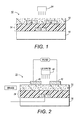
- FIG. 1 illustrates a bottom-gate bottom-contact configuration for a memory device of the present disclosure.
- the device 10 comprises a substrate 16 in contact with the gate electrode 18 and a gate dielectric layer 14.
- the gate electrode 18 is depicted here atop the substrate 16, but the gate electrode could also be located in a depression within the substrate.
- the gate dielectric layer 14 separates the gate electrode 18 from the source electrode 20, drain electrode 22, and the semiconducting layer 12.
- the semiconducting layer 12 runs over and between the source and drain electrodes 20 and 22.
- the semiconductor has a channel length between the source and drain electrodes 20 and 22.
- a light source 24 is located so as to be able to illuminate the semiconducting layer 12 between the source electrode 20 and the drain electrode 22.
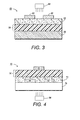
- FIG. 2 illustrates a bottom-gate top-contact configuration for a memory device of the present disclosure.
- the device 30 comprises a substrate 36 in contact with the gate electrode 38 and a gate dielectric layer 34.
- the semiconducting layer 32 is placed on top of the gate dielectric layer 34, and is separated from the gate electrode thereby.
- the source and drain electrodes 40 and 42 are then placed on top of the semiconducting layer 32.
- a light source 44 is located so as to be able to illuminate the semiconducting layer 32 between the source electrode 40 and the drain electrode 42.
- FIG. 3 illustrates a bottom-gate bottom-contact configuration for a memory device of the present disclosure.
- the device 50 comprises a substrate 56 which also acts as the gate electrode.
- the substrate is in contact with a gate dielectric layer 54.
- the semiconducting layer 52 is placed on top of the gate dielectric layer 54, and is separated from the gate electrode thereby.
- the source and drain electrodes 60 and 62 are then placed on top of the semiconducting layer 52.
- a light source 64 is located so as to be able to illuminate the semiconducting layer 52 between the source electrode 60 and the drain electrode 62.
- FIG. 4 illustrates a top-gate top-contact configuration for a memory device of the present disclosure.
- the device 70 comprises a substrate 76 in contact with the source electrode 80, drain electrode 82, and the semiconducting layer 72.
- the semiconducting layer 72 runs over and between the source and drain electrodes 80 and 82.
- the gate dielectric layer 74 is on top of the semiconducting layer 72.
- the gate electrode 78 is on top of the gate dielectric layer 74 and does not contact the semiconducting layer 72.
- a light source 84 is located so as to be able to illuminate the semiconducting layer 72 between the source electrode 80 and the drain electrode 82.
- the substrate 76 is transparent and the light source 84 illuminates the semiconducting layer 72 through the substrate.
- the semiconducting layer comprises an organic semiconductor.
- the organic semiconductor can be an organic semiconducting compound or a semiconducting polymer.
- the organic semiconductor compound may have the structure of Formula (I): wherein each R 1 is independently selected from alkyl, substituted alkyl, alkenyl, substituted alkenyl, alkynyl, substituted alkynyl, aryl, substituted aryl, heteroaryl, substituted heteroaryl, alkoxy, alkylthio, trialkylsilyl, aldehyde, cyano (-CN), and halogen; f and g are the number of R 1 sidechains on their respective phenyl or naphthyl ring, and are independently an integer from 0 to 6; X is selected from the group consisting of O, S, and Se; and a, b, and c are independently 0 or 1.
- the exterior portion of the compound when a or b is 0, the exterior portion of the compound will be a phenyl ring that may have up to 4 sidechains. When a or b is 1, the exterior portion of the compound will be a naphthyl ring that may have up to 6 sidechains.
- alkyl refers to a radical composed entirely of carbon atoms and hydrogen atoms which is fully saturated.
- the alkyl radical may be linear, branched, or cyclic. Depending on the context, the radical may be monovalent or divalent.
- alkenyl refers to a radical composed entirely of carbon atoms and hydrogen atoms which contains at least one carbon-carbon double bond. Depending on the context, the radical may be monovalent or divalent.
- alkynyl refers to a radical composed entirely of carbon atoms and hydrogen atoms which contains at least one carbon-carbon triple bond. Depending on the context, the radical may be monovalent or divalent.
- aryl refers to an aromatic radical composed entirely of carbon atoms and hydrogen atoms. When aryl is described in connection with a numerical range of carbon atoms, it should not be construed as including substituted aromatic radicals.
- aryl containing from 6 to 10 carbon atoms should be construed as referring to a phenyl group (6 carbon atoms) or a naphthyl group (10 carbon atoms) only, and should not be construed as including a methylphenyl group (7 carbon atoms).
- the radical may be monovalent or divalent.
- heteroaryl refers to an aromatic radical composed of carbon atoms, hydrogen atoms, and one or more heteroatoms.
- the carbon atoms and the heteroatoms are present in a cyclic ring or backbone of the radical.
- the heteroatoms are selected from O, S, and N.
- Exemplary heteroaryl radicals include thienyl and pyridinyl. Depending on the context, the radical may be monovalent or divalent.
- alkoxy refers to an alkyl radical which is attached to an oxygen atom, i.e. -O-C n H 2n+1 .
- alkylthio refers to an alkyl radical which is attached to a sulfur atom, i.e. -S-C n H 2n+1 .
- titanium alkylsilyl refers to a radical composed of a tetravalent silicon atom having three alkyl radicals attached to the silicon atom, i.e. -Si(R) 3 .
- the three alkyl radicals may be the same or different.
- the alkyl radicals may be substituted or unsubstituted.
- aldehyde refers to a radical of the formula -CO-R, where R is hydrogen or alkyl.
- cyano refers to a radical of the formula -CN.
- halogen refers to fluorine, chlorine, bromine, and iodine.
- substituted refers to at least one hydrogen atom on the named radical being substituted with another functional group, such as halogen, -CN, -NO 2 , -COOH, and -SO 3 H.
- An exemplary substituted alkyl group is a perhaloalkyl group, wherein one or more hydrogen atoms in an alkyl group are replaced with halogen atoms, such as fluorine, chlorine, iodine, and bromine.
- an aryl or heteroaryl group may also be substituted with alkyl or alkoxy.
- Exemplary substituted aryl groups include methylphenyl and methoxyphenyl.
- Exemplary substituted heteroaryl groups include dodecylthienyl.
- the alkyl and alkoxy groups each independently contain from 1 to 30 carbon atoms.
- the aryl groups independently contain from 6 to 30 carbon atoms.
- the molecule of Formula (I) is also formally known as a disubstituted-[1]benzothieno[3,2-b]benzothiophene.
- the [1]benzothieno[3,2-b]benzothiophene moiety (when f and g are each 0) may be abbreviated herein as "BTBT".
- the semiconductor compound of Formula (I) could be referred to as a disubstituted-BTBT.
- the disubstituted-BTBT compound has the structure of Formula (II): wherein R 2 and R 3 are independently selected from alkyl, substituted alkyl, alkenyl, substituted alkenyl, alkynyl, substituted alkynyl, aryl, substituted aryl, heteroaryl, substituted heteroaryl, alkoxy, alkylthio, trialkylsilyl, aldehyde, cyano, and halogen.
- R 2 and R 3 are independently selected from alkyl, substituted alkyl, alkenyl, substituted alkenyl, alkynyl, substituted alkynyl, aryl, substituted aryl, heteroaryl, substituted heteroaryl, alkoxy, alkylthio, trialkylsilyl, aldehyde, cyano, and halogen.
- R 2 and R 3 are independently selected from alkyl, substituted alkyl, alkenyl, substituted alkenyl, alky
- R 2 and R 3 are independently selected from alkyl and substituted alkyl.
- the compound has the structure of Formula (II-a):
- the disubstituted-BTBT compound has the structure of Formula (III): wherein R 2 and R 3 are independently selected from alkyl, substituted alkyl, alkenyl, substituted alkenyl, alkynyl, substituted alkynyl, aryl, substituted aryl, heteroaryl, substituted heteroaryl, alkoxy, alkylthio, trialkylsilyl, aldehyde, cyano, and halogen.
- R 2 and R 3 are independently selected from alkyl, substituted alkyl, alkenyl, substituted alkenyl, alkynyl, substituted alkynyl, aryl, substituted aryl, heteroaryl, substituted heteroaryl, alkoxy, alkylthio, trialkylsilyl, aldehyde, cyano, and halogen.
- R 2 and R 3 are independently selected from alkyl, substituted alkyl, alkenyl, substituted alkenyl, alkyn
- the organic semiconductor compound of Formula (I) has the structure of Formula (VI): wherein R 8 and R 9 are independently selected from alkyl, substituted alkyl, alkenyl, substituted alkenyl, alkynyl, substituted alkynyl, aryl, substituted aryl, heteroaryl, substituted heteroaryl, alkoxy, alkylthio, trialkylsilyl, aldehyde, cyano, and halogen.
- R 8 and R 9 are independently selected from alkyl, substituted alkyl, alkenyl, substituted alkenyl, alkynyl, substituted alkynyl, aryl, substituted aryl, heteroaryl, substituted heteroaryl, alkoxy, alkylthio, trialkylsilyl, aldehyde, cyano, and halogen.
- R 8 and R 9 are independently selected from alkyl, substituted alkyl, alkenyl, substituted alkenyl, alkynyl
- R 8 is halogen or cyano
- R 9 is alkyl, substituted alkyl, alkenyl, substituted alkenyl, or aldehyde.
- R 9 is halogen or cyano
- R 8 is alkyl, substituted alkyl, alkenyl, substituted alkenyl, or aldehyde.
- Z sulfur
- this compound is known as an anthra[2,3-b:6,7-b]dithiophene.
- the organic semiconductor compound of Formula (VII) has the structure of Formula (VIII): wherein R 10 and R 11 are independently selected from alkyl, substituted alkyl, alkenyl, substituted alkenyl, alkynyl, substituted alkynyl, aryl, substituted aryl, heteroaryl, substituted heteroaryl, alkoxy, alkylthio, trialkylsilyl, aldehyde, cyano, and halogen; and wherein R 12 is alkyl or substituted alkyl.
- R 10 and R 11 are independently selected from alkyl, substituted alkyl, alkenyl, substituted alkenyl, alkynyl, substituted alkynyl, aryl, substituted aryl, heteroaryl, substituted heteroaryl, alkoxy, alkylthio, trialkylsilyl, aldehyde, cyano, and halogen; and wherein R 12 is alkyl or substituted alkyl.
- methods of producing the compound of Formula (II) include reacting a 3,8-dihalo-BTBT A with an alkyne to form a 3,8-dialkyn-1-yl-BTBT 1.
- This initial reaction is illustrated below: wherein X is a halogen, R is alkyl, Ph(PPh 3 ) 2 Cl 2 is bis(triphenylphosphine) palladium(II) chloride, CuI is copper iodide, and iPr 2 NH is diisopropylamine.
- the two R groups are identical.
- the two R groups can be different as well, for example by using a blocking/protecting group on one of the X groups, performing a first reaction with a first alkyne to convert the unprotected X group, removing the blocking/protecting group, then subsequently performing a second reaction with a second different alkyne.
- the 3,8-dialkyn-1-yl-BTBT 1 can be reduced to a 3,8-dialkyl-[1]benzothieno[3,2-b]benzothiophene 1a as depicted below: wherein Pd/C is a palladium on carbon catalyst and THF is tetrahydrofuran. Similar reactions can be performed for the other possible R a substituents.
- Methods for preparing compounds 1a also includes the reaction of the [1]benzothieno[3,2-b]-benzothiophene core B with a susbstituted acid chloride in presence of aluminum trichloride to form a 3,8-diketonyl BTBT 2.
- dialdehyde BTBT 2 is deoxygenated using a modified Wolff-Kishner reduction using hydrazine in the presence of potassium hydroxide in diethylene glycol. This forms 3,8-dialkyl-[1]benzothieno[3,2-b]benzothiophene 1b.
- This 2-step method is particularly effective for short R substituents (C 2 -C 8 ).
- the organic semiconductor in the semiconducting layer can be a semiconducting polymer.
- semiconducting polymers include for example, poly(triarylamine)s, polythiophenes, poly(p-phenylene vinylene), polypyrroles, polyanilines, polyfluorenes, polypyrenes, diketopyrrolopyrrole copolymers, and poly(3,4-ethylenedioxythiophene).
- the semiconducting polymers disclosed in U.S. Patent Nos. 7,932,344 and 8,558,109 illustrate some polymers which can be used, and are fully incorporated by reference herein.
- the organic semiconductor may have a band gap of from about 1.2 to about 3.5 eV, including from about 1.8 to about 3.5 eV or from about 2.0 to about 3.5 eV. In some embodiments, the organic semiconductor may have a wide band gap of from about 2.5 (absorbance less than 500 nm) to about 3.5 eV.
- the organic semiconductor has a crystalline or liquid crystalline structure.
- the semiconductor compounds of Formulas (I) or (VII) are colorless in the visible region of the electromagnetic spectrum (i.e. from 390 nm to 750 nm). Colorless semiconductors not only provide excellent stability due to their large band gaps, but also offer advantage in transparency for transparent device applications. In the present disclosure, colorless semiconductors provide excellent transparency for photons to reach the photo-responsive moieties of the photo-responsive material in the semiconducting layer.
- the semiconducting layer also includes a photo-responsive material.
- the photo-responsive material may be present as a photo-responsive compound or in a photo-responsive polymer.
- a photo-responsive moiety is part of the photo-responsive material.
- photo-responsive means that the moiety will, upon external stimulation such as exposure to irradiation at a suitable wavelength, undergo a reversible structural change.
- the irradiation is performed using a laser with wavelength from about 190 nm to about 1090 nm. More specifically, the irradiation is of ultraviolet light, having a maximum wavelength ( ⁇ max ) of 400 nanometers to 190 nanometers.
- the light source for illuminating the semiconducting layer and the photo-responsive material therein can be any structure known in the art, such as a light emitting diode (LED), light guide, light bulb, lamp, etc.
- the irradiation is performed using a pulse laser; in other embodiments, the irradiation is performed using a continuous wave (CW) laser.
- the photo-responsive material undergoes cis-trans isomerization upon exposure to irradiation.
- the photo-responsive compound can be any compound other than a spiropyran compound.
- the photo-responsive compound can be an azobenzene, a coumarin, a cinnamate, a dithiazolylarylene, a diarylethene, a stilbene, or an aromatic Schiff base.
- An azobenzene, stilbene, or aromatic Schiff base can be generally represented by the structure of Formula (A): wherein each R b and R c is independently selected from alkyl, substituted alkyl, alkenyl, substituted alkenyl, alkynyl, substituted alkynyl, heteroaryl, substituted heteroaryl, alkoxy, alkylthio, trialkylsilyl, aldehyde, cyano, halogen, hydroxyl, amino, thiol, or nitro; u and v are independently integers from 0 to 4; D is an electron donor group; E is an electron acceptor group; and each Y is independently N or CH.
- R b and R c is independently selected from alkyl, substituted alkyl, alkenyl, substituted alkenyl, alkynyl, substituted alkynyl, heteroaryl, substituted heteroaryl, alkoxy, alkylthio, trialkylsilyl, aldehyde
- Formula (A) is an azobenzene.
- Formula (A) is a stilbene.
- Formula (A) is an aromatic Schiff base.
- An example of an azobenzene is the dye Disperse Red 1.
- hydroxyl refers to a radical of the formula -OH.
- amino refers to a radical of the formula -NR 1 R 2 , wherein R 1 and R 2 are independently hydrogen or alkyl, or to a radical of the formula-N + R 1 R 2 R 3 , wherein R 1 , R 2 , and R 3 are independently hydrogen or alkyl.
- this second radical is sometimes referred to as an "ammonium" ion.
- An amino radical may also be divalent, i.e. -(NR 1 )-.
- thiol refers to a radical of the formula -SH.
- nitro refers to a radical of the formula -NO 2 .
- An electron donor group has high electron density.
- Exemplary electron donor groups include hydroxyl, amino, alkoxy, alkyl, aryl, vinyl, and combinations thereof.
- An electron acceptor group has low electron density.
- Exemplary electron acceptor groups include halogen, aldehyde, carboxyl, perfluoroalkyl, cyano, nitro, sulfinyl, sulfonyl, and combinations thereof.
- Hydrogen can be considered either an electron donor or an electron acceptor.
- Carboxyl refers to a radical of the formula -CO-OR, where R is hydrogen or alkyl.
- sulfinyl refers to a radical of the formula -SO-X, where X is a halogen.
- sulfonyl refers to a radical of the formula -SO2-X, where X is a halogen.
- a coumarin can be represented by the structure of Formula (B): wherein R 1 , R 2 , R 3 , and R 4 are independently hydrogen, alkyl, substituted alkyl, alkenyl, substituted alkenyl, alkynyl, substituted alkynyl, aryl, substituted aryl, heteroaryl, substituted heteroaryl, alkoxy, alkylthio, trialkylsilyl, aldehyde, cyano, halogen, hydroxyl, amino, thiol, or nitro, or wherein R groups can be joined together to form a ring.
- R groups can be joined together to form a ring.
- a cinnamate can be represented by the structure of Formula (C): wherein R 1 , R 2 , and R 3 are independently hydrogen, alkyl, substituted alkyl, alkenyl, substituted alkenyl, alkynyl, substituted alkynyl, aryl, substituted aryl, heteroaryl, substituted heteroaryl, alkoxy, alkylthio, trialkylsilyl, aldehyde, cyano, halogen, hydroxyl, amino, thiol, or nitro, or wherein R groups can be joined together to form a ring (particularly R 2 and R 3 ). Similar to coumarin, cinnamate can undergo 2+2 cyclization reaction upon irradiation.
- a dithiazolylarylene can be represented by the structure of Formula (D): wherein R 1 , R 3 , R 4 , and R 6 are independently hydrogen, alkyl, substituted alkyl, alkenyl, substituted alkenyl, alkynyl, substituted alkynyl, aryl, substituted aryl, heteroaryl, substituted heteroaryl, alkoxy, alkylthio, trialkylsilyl, aldehyde, cyano, halogen, hydroxyl, amino, thiol, or nitro, or wherein R groups can be joined together to form a ring.
- R groups can be joined together to form a ring.
- a diarylethene can be represented by the structure of Formula (E): wherein Z is independently O, S, or NR; and R 1 , R 2 , R 3 , R 4 , R 5 , R 6 , R 7 , and R 8 are independently hydrogen, alkyl, substituted alkyl, alkenyl, substituted alkenyl, alkynyl, substituted alkynyl, aryl, substituted aryl, heteroaryl, substituted heteroaryl, alkoxy, alkylthio, trialkylsilyl, aldehyde, cyano, halogen, hydroxyl, amino, thiol, or nitro; and wherein two adjacent R groups can be joined together to form a ring.
- R 1 , R 2 , R 3 , R 4 , R 5 , R 6 , R 7 , and R 8 are independently hydrogen, alkyl, substituted alkyl, alkenyl, substituted alkenyl, alkynyl, substituted al
- R 2 and R 3 can form a phenyl ring
- R 5 and R 6 can form a phenyl ring
- R 7 and R 8 form a ring.
- the photo-responsive moiety is usually present as a pendant group (i.e. sidechain).
- the photo-responsive polymer includes a backbone with pendant groups attached thereto, and the pendant groups include the moiety that will undergo the reversible structural change.
- the photo-responsive polymer can be considered as forming a matrix within which the organic semiconductor compound is dispersed.
- the photo-responsive polymer includes pendant groups that undergo cis-trans isomerization upon exposure to irradiation.
- the photo-responsive moiety is present in the backbone of the photo-responsive polymer.
- such photo-responsive polymers are disclosed in Macromolecules, 2004, vol 37, pp 6090 , and Macromolecules, 2001, vol 34, pp. 7822 .
- the photo-responsive moiety in a photo-responsive polymer, can be selected from the group consisting of an azobenzene group, a spiropyran group, a coumarin group, a cinnamate group, a dithiazolylarylene group, a diarylethene group, a stilbene group, and an aromatic Shiff base group.
- these groups are as depicted above in Formulas (A)-(E), with one of the R groups including a linkage to the polymer backbone.
- a spiropyran group has the structure of Formula (F): wherein R 5 , R 6 , R 7 , and R 8 are independently hydrogen, alkyl, substituted alkyl, alkenyl, substituted alkenyl, alkynyl, substituted alkynyl, aryl, substituted aryl, heteroaryl, substituted heteroaryl, alkoxy, alkylthio, trialkylsilyl, aldehyde, cyano, halogen, hydroxyl, amino, thiol, or nitro; each R is independently selected from the same groups as described above for R 5 except for hydrogen and m and n are independently integers from 0 to 4. One of the R groups will form a linkage to the polymer backbone.
- the photo-responsive polymer includes a monomer of Formula (G): wherein A is hydrogen, alkyl, or halogen; L is a divalent linkage; R a is hydrogen or alkyl; each R b and R c is independently selected from alkyl, substituted alkyl, alkenyl, substituted alkenyl, alkynyl, substituted alkynyl, heteroaryl, substituted heteroaryl, alkoxy, alkylthio, trialkylsilyl, aldehyde, cyano, halogen, hydroxyl, amino, thiol, or nitro; v is an integer from 0 to 4; w is an integer from 0 to 5; and each Y is independently N or CH.
- A is hydrogen, alkyl, or halogen
- L is a divalent linkage
- R a is hydrogen or alkyl
- each R b and R c is independently selected from alkyl, substituted alkyl, alkenyl, substituted al
- divalent linkage refers to any moiety which is able to form a single bond with two different non-hydrogen atoms, joining those two different atoms together.
- a divalent linkage can be formed from the combination of different radicals, for example from the combination of an ester (-CO-O-) group and an alkyl group.
- An exemplary divalent linkage is -CO-O-(CH 2 ) m -, where m is an integer from 1 to 6.
- the monomer of Formula (G) will undergo polymerization through the vinyl group.
- the pendant group will contain either a stilbene group or an azobenzene group, which can undergo cis-trans isomerization upon irradiation.
- Y is nitrogen, i.e. the pendant group contains an azobenzene group.
- a specific example is the monomer of Formula (G-1), which is also known as Disperse Red 1 methacrylate:
- the photo-responsive polymer can be a copolymer or a dipolymer.
- copolymer is used herein to refer to a polymer having two or more monomers, while the term “dipolymer” is used to refer to a polymer having only two monomers.
- the monomer of Formula (G) may be from about 1 mole% to about 50 mole% of the copolymer, including from about 5 to about 15 mol% of the copolymer.
- the photo-responsive polymer includes an acrylate co-monomer along with the monomer of Formula (G).
- An acrylate monomer has the structure of Formula (H): where R d is alkyl; and R e is hydrogen, alkyl, or halogen.
- exemplary co-monomers include methyl methacrylate and methyl acrylate.
- One exemplary photo-responsive polymer is a copolymer of Disperse Red 1 methacrylate and methyl methacrylate, as illustrated in Formula (a): where x and y are the mole fraction of the respective monomer, and each have a value between 0 and 1 (exclusive).
- x is from about 0.05 to about 0.15
- y is from about 0.85 to about 0.95.
- the molar ratio of x:y can be from about 1:19 to about 3:17, and in some particular embodiments is about 1:10.
- the photo-responsive polymer may have a weight average molecular weight of 2,000 to about 2,000,000, including from about 4,000 to about 1,000,000, when measured according to gel permeation chromatography (GPC) using polystyrene standards.
- the weight ratio of the organic semiconductor compound to the photo-responsive polymer in the semiconducting layer can be from about 25:75 to about 95:5, including from about 25:75 to about 75:25.
- the semiconducting layer comprises an organic semiconducting compound and a photo-responsive polymer as described above. In other specific embodiments, the semiconducting layer comprises an organic semiconducting polymer and a photo-responsive compound that is not a spiropyran, as described above.
- a non-photo-responsive polymer resin is usually included as a binder, but is optional.
- Exemplary non-photo-responsive polymer resins include the acrylates such as poly(methyl methacrylate), and polystyrene, and the like.
- the difference between the HOMO level of the organic semiconductor and the HOMO level of the photo-responsive polymer is not greater than 0.5 eV, and is preferably less than 0.3 eV.
- the difference between the HOMO level of the organic semiconductor and the HOMO level of the photo-responsive compound is not greater than 0.5 eV, and is preferably less than 0.3 eV.
- the semiconducting layer can be formed from a semiconductor solution containing the organic semiconductor (compound or polymer), the photo-responsive moiety (compound or polymer), and a solvent in which both are soluble.
- exemplary solvents used in the solution may include chlorinated solvents such as chlorobenzene, chlorotoluene, dichlorobenzene, dichloroethane, chloroform, trichlorobenzene, and the like; alcohols and diols such as propanol, butanol, hexanol, hexanediol, etc.; hydrocarbons or aromatic hydrocarbons such as hexane, heptane, toluene, decalin, xylene, ethyl benzene, tetrahydronaphthalene, methyl nanphthalene, mesitylene, trimethyl benzene, etc.; ketones such as acetone, methyl ethyl ketone,
- the organic semiconductor and the photo-responsive moiety are from about 0.05 to about 20 weight percent of the semiconductor solution, including from about 0.1 to about 10 weight percent of the semiconductor solution, or from about 1 to about 5 weight percent of the semiconductor solution. It is noted that when the molecular weight of the photo-responsive polymer is higher, the viscosity of the solution will be greater. This can help when forming a uniform semiconducting layer using solution deposition techniques such as inkjet printing and spin coating.
- the semiconducting layer may be formed in the memory device using conventional processes known in the art.
- the semiconducting layer is formed using solution depositing techniques.
- Exemplary solution depositing techniques include spin coating, blade coating, rod coating, dip coating, screen printing, ink jet printing, stamping, stencil printing, screen printing, gravure printing, flexography printing, and the like.
- the semiconductor solution is optionally thermally treated (for example, by drying or annealing) at an elevated temperature which is lower than the melting point of the organic semiconductor.
- the thermal treatment may be carried out at a temperature of less than 200°C, less than 150°C, or less than 100°C.
- the semiconducting layer formed using the semiconductor solution can be from about 5 nanometers to about 1000 nanometers deep, including from about 20 to about 100 nanometers in depth. In certain configurations, such as the configurations shown in FIG. 1 and FIG. 4 , the semiconducting layer completely covers the source and drain electrodes.
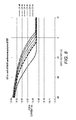
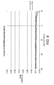
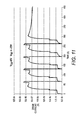
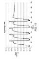
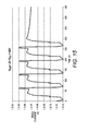
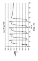
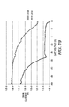
- a memory device using the semiconducting layer described herein can be operated as follows, with reference to FIG. 2 .
- Two electrodes source and drain contact the semiconducting layer, and the resistance/current between these two electrodes is read.
- the resistance can be switched from a first or "original” state to a second or “activated” state by irradiation with UV light. In the original state, the resistance is high and the current is low. In the activated state, the resistance is low and the current is high.
- the current will increase substantially upon irradiation.
- the device will remain in the activated state when the light source is then turned off.
- the gate bias will have a first value, which is relatively low, between 0V and about -5V.
- a large voltage for example from a second value of -20V to -60V
- an intermediate state will exist in which the current further increases.
- the gate bias voltage then returns to the first value, the device will return to the original state.
- the second value of the gate bias voltage has a greater absolute magnitude than the first value of the gate bias voltage.
- the strong donor-acceptor photo-responsive moieties create charge trapping sites in the semiconducting layer.
- the charge carriers are trapped around the azobenzene/stilbene moieties of the polymer.
- the isomerization from lower-energy trans state to higher-energy cis state
- the photovoltaic effect will cause the charge carriers to be released, resulting in high current.
- the memory device can be operated at various conditions.
- the device can be operated with a source/drain voltage from about -5V to about-60V, and the gate bias can be from about 0V to about -5V.
- the memory device is very similar to a thin film transistor and generally includes a substrate, an optional gate electrode, source electrode, drain electrode, and a dielectric layer in addition to the semiconducting layer.
- the substrate may be composed of materials including but not limited to silicon, glass plate, plastic film or sheet.
- plastic substrate such as for example polyester, polycarbonate, polyimide sheets and the like may be preferred.
- the thickness of the substrate may be from about 10 micrometers to over 10 millimeters with an exemplary thickness being from about 50 to about 100 micrometers, especially for a flexible plastic substrate and from about 0.5 to about 10 millimeters for a rigid substrate such as glass or silicon.
- the substrate may be opaque, or can be transparent so that ultraviolet light can pass through the substrate.
- the dielectric layer generally can be an inorganic material film, an organic polymer film, or an organic-inorganic composite film.
- inorganic materials suitable as the dielectric layer include silicon oxide, silicon nitride, aluminum oxide, barium titanate, barium zirconium titanate and the like.
- suitable organic polymers include polyesters, polycarbonates, poly(vinyl phenol), polyimides, polystyrene, polymethacrylates, polyacrylates, epoxy resin and the like.
- the thickness of the dielectric layer depends on the dielectric constant of the material used and can be, for example, from about 10 nanometers to about 500 nanometers.
- the dielectric layer may have a conductivity that is, for example, less than about 10 -12 Siemens per centimeter (S/cm).
- the dielectric layer is formed using conventional processes known in the art, including those processes described in forming the gate electrode.
- the dielectric layer may be surface modified with a surface modifier.
- the semiconducting layer can be directly contacted with this modified dielectric layer surface. The contact may be complete or partial. This surface modification can also be considered as forming an interfacial layer between the dielectric layer and the semiconducting layer.
- Exemplary surface modifying agents include organosilanes such as hexamethyldisilazane and octyltrichlorosilane.
- the gate electrode is composed of an electrically conductive material. It can be a thin metal film, a conducting polymer film, a conducting film made from conducting ink or paste, or the substrate itself, for example heavily doped silicon.
- Examples of gate electrode materials include but are not restricted to aluminum, gold, silver, chromium, indium tin oxide, conductive polymers such as polystyrene sulfonate-doped poly(3,4-ethylenedioxythiophene) (PSS-PEDOT), and conducting ink/paste comprised of carbon black/graphite.
- the gate electrode can be prepared by vacuum evaporation, sputtering of metals or conductive metal oxides, conventional lithography and etching, chemical vapor deposition, spin coating, casting or printing, or other deposition processes.
- the thickness of the gate electrode ranges for example from about 10 to about 200 nanometers for metal films and from about 1 to about 10 micrometers for conductive polymers.
- Typical materials suitable for use as source and drain electrodes include those of the gate electrode materials such as aluminum, gold, silver, chromium, zinc, indium, conductive metal oxides such as zinc-gallium oxide, indium tin oxide, indium-antimony oxide, conducting polymers and conducting inks.
- Typical thicknesses of source and drain electrodes are, for example, from about 40 nanometers to about 1 micrometer, including more specific thicknesses of from about 100 to about 400 nanometers.
- Typical materials suitable for use as source and drain electrodes include those of the gate electrode materials such as gold, silver, nickel, aluminum, platinum, conducting polymers, and conducting inks.
- the electrode materials provide low contact resistance.
- Typical thicknesses are about, for example, from about 40 nanometers to about 1 micrometer with a more specific thickness being about 100 to about 400 nanometers.
- the devices of the present disclosure contain a semiconductor channel.
- the semiconductor channel width may be, for example, from about 5 micrometers to about 5 millimeters with a specific channel width being about 100 micrometers to about 1 millimeter.
- the semiconductor channel length may be, for example, from about 1 micrometer to about 1 millimeter with a more specific channel length being from about 5 micrometers to about 100 micrometers.
- the various components of the memory device may be deposited upon the substrate in any order.
- the gate electrode and the semiconducting layer should both be in contact with the gate dielectric layer.
- the source and drain electrodes should both be in contact with the semiconducting layer.
- the phrase "in any order" includes sequential and simultaneous formation.
- the source electrode and the drain electrode can be formed simultaneously or sequentially.
- the term "on” or “upon” the substrate refers to the various layers and components with reference to the substrate as being the bottom or support for the layers and components which are on top of it. In other words, all of the components are on the substrate, even though they do not all directly contact the substrate.
- both the dielectric layer and the semiconducting layer are on the substrate, even though one layer is closer to the substrate than the other layer.
- the resulting TFT has good mobility and good current on/off ratio.
- various materials were studied. They include the copolymer of Formula (a), 3,8-dipentyl-BTBT, azobenzene, and poly(methyl methacrylate) (PMMA), as illustrated below.
- the azobenzene repeat unit was about 10 mole% of the copolymer (i.e. x ⁇ 0.10).
- an azobenzene compound and PMMA were used.
- Memory devices were fabricated in a similar manner to an organic thin film transistor.
- N-doped silicon with a 200-nm silicon oxide layer was used as the substrate.
- the surface of the silicon oxide layer was modified with HMDS, yielding a self-assembled monolayer.
- a semiconductor composition was prepared, comprising 1.0 wt% dipentyl-BTBT and 1.0 wt% of the polymer of Formula (a) in a chlorobenzene solvent.
- the semiconductor composition was spin coated on top of the modified HMDS layer at 3000 rpm, forming about semiconducting layer of about 50 nanometers (nm) in thickness.
- the substrate/semiconducting layer was dried in a vacuum oven at 70°C for 30 minutes.
- Gold source and drain electrodes were vapor-evaporated onto the semiconducting layer through a shadow mask.
- the device had a channel length (gap between the source/drain electrodes) of 90 micrometers, and had a channel width (the length of the electrodes) of 1 millimeter (mm).
- the device was operated in standard transistor mode by applying a drain voltage of -60 V and sweeping the gate voltage from +20 V to -60 V. Referring to FIG. 5 , the device turned on at gate voltage about -50 V. At low gate voltage from about -40 V to 0 V, the current was very low. Upon irradiating the semiconducting layer with a UV light, the current increased dramatically, particularly at low gate bias. Therefore, the device should be able to switch between an "on” and an "off” state at low or no gate bias (indicated by the arrows) by irradiating with UV light to "write", and applying a large gate bias to "erase” the bi-stable states.
- FIG. 6 shows the device operating in memory mode.
- the device At no gate bias and a reading voltage of -20V, the device originally was at off state, having a very low current less than 10 -11 A (time around zero seconds).
- the device Upon irradiating with UV light at approximately 25 seconds, the device was turned on and the current increased dramatically to 10 -6 A, an on/off ratio > 10 5 .
- the UV light was turned off at about 40 seconds, and the current remained high ( ⁇ 10 -6 A).
- a slow decay of the current was observed.
- the gate bias was set back to 0 at about 70 seconds, the device returned to its original low-current state. This was repeated, and the graph shows very reproducible on/off behavior. It should be noted that all measurements were performed in ambient conditions. The device was stable for a few weeks upon writing and erasing for thousands of
- the azobenzene compound was mixed with PMMA and dipentyl-BTBT in a weight ratio of 45:5:50 PMMA:azobenzene:BTBT (to obtain a similar amount of azobenzene compared to the polymer in Example 1), and tested.
- the results are shown in FIG. 8 .
- the turn-on voltage shifted towards the positive regime (i.e. to the right), and the current increased at low gate bias.
- the magnitude of shifting and the current enhancement was much smaller than the system using a photo-responsive polymer. Compare FIG. 5 to FIG. 8 . This indicated that a photo-responsive material was needed, and that the design of the photo-responsive material affected the on/off ratio.
- Using a polymer containing the azobenzene moiety was more effective than just using azobenzene as a compound.
- the memory device of Example 1 was operated at various conditions such as source/drain voltage from about -5 to about -60V, and gate bias from about 0 to about -5 V.
- the source/drain voltage is measured between the source and drain electrodes
- the gate bias voltage is measured between the source and gate electrodes.
- the I-V curves for different combinations of these conditions are shown in FIGs. 10-18 . In all cases, high current on/off ratio and very reproducible on/off behavior could be achieved, indicating very robust operating conditions.
- Disperse Red 1 is illustrated below:
- the device was operated by applying a drain voltage of -60 V and sweeping the gate voltage from +20 V to -60 V, with UV on and UV off.
- the results are shown in FIG. 19 , and are comparable to those exhibited in FIG. 5 . Therefore, the device should be able to switch between an "on” and an “off” state at low or no gate bias (indicated by the arrows) by irradiating with UV light to "write", and applying a large gate bias to "erase” the bi-stable states.
- the device was then operated with a source/drain voltage of -60 V and a gate bias of -5 V.
- the I-V curve is shown in FIG. 20 , and indicates both high on/off current ratio and reproducibility.
- FIG. 21 is a graph of current versus time for a semiconducting layer containing a 50:50 weight ratio of dipentyl-BTBT and the polymer of Formula (a), with a performance corresponding to FIG. 5 .
- FIG. 22 is a graph of current versus time for a semiconducting layer containing Disperse Red 1, PMMA, and dipentyl-BTBT in a weight ratio of 5:45:50. Both devices were operated with a source/drain voltage of -60 V and a gate bias of -5 V.
- FIG. 21 shows that the system of a semiconducting compound and a photo-responsive polymer has a long retention time, with a slow decay of the current over a long period of over 30 minutes. This long retention is desirable for memory applications.
- the system containing a semiconducting compound and a photo-responsive compound showed a very short retention time, as seen by the current decaying rapidly to its original state in FIG. 22 .
- This system could be used for a DRAM type of application. Alternatively, this system could be used as an optical sensor device rather than a memory device.
Landscapes
- Physics & Mathematics (AREA)
- Electromagnetism (AREA)
- Chemical & Material Sciences (AREA)
- Engineering & Computer Science (AREA)
- Composite Materials (AREA)
- Materials Engineering (AREA)
- Thin Film Transistor (AREA)
- Electroluminescent Light Sources (AREA)
- Semiconductor Memories (AREA)
Applications Claiming Priority (1)
| Application Number | Priority Date | Filing Date | Title |
|---|---|---|---|
| US14/098,330 US10381583B2 (en) | 2013-12-05 | 2013-12-05 | Electronic device |
Publications (1)
| Publication Number | Publication Date |
|---|---|
| EP2882005A1 true EP2882005A1 (en) | 2015-06-10 |
Family
ID=51951705
Family Applications (1)
| Application Number | Title | Priority Date | Filing Date |
|---|---|---|---|
| EP14194525.3A Withdrawn EP2882005A1 (en) | 2013-12-05 | 2014-11-24 | Electronic device |
Country Status (3)
| Country | Link |
|---|---|
| US (1) | US10381583B2 (cg-RX-API-DMAC7.html) |
| EP (1) | EP2882005A1 (cg-RX-API-DMAC7.html) |
| JP (1) | JP6456122B2 (cg-RX-API-DMAC7.html) |
Cited By (1)
| Publication number | Priority date | Publication date | Assignee | Title |
|---|---|---|---|---|
| CN112825259A (zh) * | 2019-11-20 | 2021-05-21 | 三星电子株式会社 | 非易失性存储器及其操作方法 |
Families Citing this family (3)
| Publication number | Priority date | Publication date | Assignee | Title |
|---|---|---|---|---|
| CN104212201B (zh) * | 2014-08-06 | 2017-04-05 | 京东方科技集团股份有限公司 | 聚合物染料及其制备方法、光阻组合物和显示装置 |
| WO2017100727A1 (en) * | 2015-12-10 | 2017-06-15 | Massachusetts Institute Of Technology | Polymer based solid -state solar thermal fuels |
| US10767069B2 (en) | 2018-05-01 | 2020-09-08 | Xerox Corporation | Aqueous carbon nanoparticle ink composition for resistors |
Citations (3)
| Publication number | Priority date | Publication date | Assignee | Title |
|---|---|---|---|---|
| US7932344B2 (en) | 2007-09-06 | 2011-04-26 | Xerox Corporation | Diketopyrrolopyrrole-based polymers |
| WO2013041822A1 (en) * | 2011-09-20 | 2013-03-28 | Cambridge Display Technology Limited | Organic semiconductor composition and organic transistor |
| US8558109B2 (en) | 2012-03-19 | 2013-10-15 | Xerox Corporation | Semiconductor composition for high performance organic devices |
Family Cites Families (10)
| Publication number | Priority date | Publication date | Assignee | Title |
|---|---|---|---|---|
| US5173381A (en) | 1991-08-05 | 1992-12-22 | Queen's University | Azo polymers for reversible optical storage |
| DE4232394A1 (de) | 1992-09-26 | 1994-03-31 | Basf Ag | Copolymerisate mit nichtlinear optischen Eigenschaften und deren Verwendung |
| US20050038143A1 (en) * | 2001-09-04 | 2005-02-17 | Shlomo Yitzchaik | Photoresponsive polymer systems and their use |
| JP2005093921A (ja) * | 2003-09-19 | 2005-04-07 | Canon Inc | 電界効果型有機トランジスタおよびその製造方法 |
| EP1783781A3 (en) * | 2003-11-28 | 2007-10-03 | Merck Patent GmbH | Organic semiconducting layer formulations comprising polyacenes and organic binder polymers |
| JP2007027366A (ja) * | 2005-07-15 | 2007-02-01 | Fujifilm Holdings Corp | 電界効果型トランジスタ及びその製造方法 |
| US8963131B2 (en) * | 2011-06-13 | 2015-02-24 | Samsung Electronics Co., Ltd. | Electronic device |
| EP2898552B1 (en) * | 2012-09-24 | 2016-03-23 | Wake Forest University | Organic thin film transistors and methods of making the same |
| US9331293B2 (en) * | 2013-03-14 | 2016-05-03 | Nutech Ventures | Floating-gate transistor photodetector with light absorbing layer |
| JP6210530B2 (ja) * | 2013-06-04 | 2017-10-11 | 国立研究開発法人物質・材料研究機構 | デュアルゲート有機薄膜トランジスタ |
-
2013
- 2013-12-05 US US14/098,330 patent/US10381583B2/en active Active
-
2014
- 2014-11-24 EP EP14194525.3A patent/EP2882005A1/en not_active Withdrawn
- 2014-11-26 JP JP2014239127A patent/JP6456122B2/ja not_active Expired - Fee Related
Patent Citations (3)
| Publication number | Priority date | Publication date | Assignee | Title |
|---|---|---|---|---|
| US7932344B2 (en) | 2007-09-06 | 2011-04-26 | Xerox Corporation | Diketopyrrolopyrrole-based polymers |
| WO2013041822A1 (en) * | 2011-09-20 | 2013-03-28 | Cambridge Display Technology Limited | Organic semiconductor composition and organic transistor |
| US8558109B2 (en) | 2012-03-19 | 2013-10-15 | Xerox Corporation | Semiconductor composition for high performance organic devices |
Non-Patent Citations (4)
| Title |
|---|
| MACROMOLECULES, vol. 34, 2001, pages 7822 |
| MACROMOLECULES, vol. 37, 2004, pages 6090 |
| MARJANOVIC N ET AL: "Photoresponse of organic field-effect transistors based on conjugated polymer/fullerene blends", ORGANIC ELECTRONICS, ELSEVIER, AMSTERDAM, NL, vol. 7, no. 4, 7 February 2006 (2006-02-07), pages 188 - 194, XP024972771, ISSN: 1566-1199, [retrieved on 20060801], DOI: 10.1016/J.ORGEL.2006.01.002 * |
| NAYOOL SHIN ET AL: "Vertically Segregated Structure and Properties of Small Molecule-Polymer Blend Semiconductors for Organic Thin-Film Transistors", ADVANCED FUNCTIONAL MATERIALS, WILEY - V C H VERLAG GMBH & CO. KGAA, DE, vol. 23, no. 3, 21 January 2013 (2013-01-21), pages 366 - 376, XP001581840, ISSN: 1616-301X, [retrieved on 20120827], DOI: 10.1002/ADFM.201201389 * |
Cited By (4)
| Publication number | Priority date | Publication date | Assignee | Title |
|---|---|---|---|---|
| CN112825259A (zh) * | 2019-11-20 | 2021-05-21 | 三星电子株式会社 | 非易失性存储器及其操作方法 |
| EP3826016A1 (en) * | 2019-11-20 | 2021-05-26 | Samsung Electronics Co., Ltd. | Nonvolatile memory device and operating method of the same |
| US11600774B2 (en) | 2019-11-20 | 2023-03-07 | Samsung Electronics Co., Ltd. | Nonvolatile memory device and operating method of the same |
| US12268106B2 (en) | 2019-11-20 | 2025-04-01 | Samsung Electronics Co., Ltd. | Nonvolatile memory device and operating method of the same |
Also Published As
| Publication number | Publication date |
|---|---|
| JP6456122B2 (ja) | 2019-01-23 |
| JP2015109442A (ja) | 2015-06-11 |
| US20150162555A1 (en) | 2015-06-11 |
| US10381583B2 (en) | 2019-08-13 |
Similar Documents
| Publication | Publication Date | Title |
|---|---|---|
| Wakayama et al. | Photochromism for optically functionalized organic field-effect transistors: a comprehensive review | |
| Ling et al. | Polymer memories: Bistable electrical switching and device performance | |
| Fang et al. | New donor− acceptor random copolymers with pendent triphenylamine and 1, 3, 4-oxadiazole for high-performance memory device applications | |
| EP2111654B1 (en) | Organic transistor using thiazolothiazole derivatives and method for fabricating the same | |
| Fang et al. | New random copolymers with pendant carbazole donor and 1, 3, 4-oxadiazole acceptor for high performance memory device applications | |
| Chou et al. | Nonvolatile organic field-effect transistor memory devices using polymer electrets with different thiophene chain lengths | |
| US8089062B2 (en) | Wax encapsulated electronic devices | |
| EP2966702A1 (en) | Organic semiconductor thin film production method | |
| JP5913107B2 (ja) | 有機半導体材料、有機半導体組成物、有機薄膜及び電界効果トランジスタ並びにその製造方法 | |
| KR101120450B1 (ko) | 절연층, 전자 디바이스, 전계 효과 트랜지스터 및 폴리비닐티오페놀 | |
| Zhang et al. | Phototunable and photopatternable polymer semiconductors | |
| EP2882005A1 (en) | Electronic device | |
| Dashitsyrenova et al. | Molecular structure–electrical performance relationship for OFET-based memory elements comprising unsymmetrical photochromic diarylethenes | |
| Sun et al. | BODIPY-based conjugated polymer covalently grafted reduced graphene oxide for flexible nonvolatile memory devices | |
| Khan et al. | Novel Porphyrin–Perylene diimide for ultrafast high-performance resistive memory devices | |
| JP5470686B2 (ja) | 絶縁層、電子デバイス、電界効果トランジスタ及びポリビニルチオフェノール | |
| Chung et al. | Random styrenic copolymers with pendant pyrene moieties: Synthesis and applications in organic field‐effect transistor memory | |
| CN104488103A (zh) | 半导体装置和制备的方法 | |
| KR20120116971A (ko) | 유기 반도체 재료 및 전계 효과 트랜지스터 그리고 그의 제조 방법 | |
| Liu et al. | Preparation of TCPP: block copolymer composites and study of their memory behavior by tuning the loading ratio of TCPP in the polymer matrix | |
| KR20080089949A (ko) | 트리페닐아민 코어를 가지는 덴드리머, 이를 이용한 유기메모리 소자 및 그의 제조방법 | |
| Ye et al. | Initiator-changed memory type: preparation of end-functionalized polymers by ATRP and study of their nonvolatile memory effects | |
| Zeng et al. | Synthesis and memory performance of a conjugated polymer with an integrated fluorene, carbazole and oxadiazole backbone | |
| KR101792394B1 (ko) | 중합체 | |
| Usta¹ | Organic semiconductors for transparent electronics |
Legal Events
| Date | Code | Title | Description |
|---|---|---|---|
| PUAI | Public reference made under article 153(3) epc to a published international application that has entered the european phase |
Free format text: ORIGINAL CODE: 0009012 |
|
| 17P | Request for examination filed |
Effective date: 20141124 |
|
| AK | Designated contracting states |
Kind code of ref document: A1 Designated state(s): AL AT BE BG CH CY CZ DE DK EE ES FI FR GB GR HR HU IE IS IT LI LT LU LV MC MK MT NL NO PL PT RO RS SE SI SK SM TR |
|
| AX | Request for extension of the european patent |
Extension state: BA ME |
|
| R17P | Request for examination filed (corrected) |
Effective date: 20151210 |
|
| RBV | Designated contracting states (corrected) |
Designated state(s): AL AT BE BG CH CY CZ DE DK EE ES FI FR GB GR HR HU IE IS IT LI LT LU LV MC MK MT NL NO PL PT RO RS SE SI SK SM TR |
|
| STAA | Information on the status of an ep patent application or granted ep patent |
Free format text: STATUS: EXAMINATION IS IN PROGRESS |
|
| 17Q | First examination report despatched |
Effective date: 20190625 |
|
| RIC1 | Information provided on ipc code assigned before grant |
Ipc: H01L 51/42 20060101ALI20200326BHEP Ipc: H01L 27/28 20060101ALN20200326BHEP Ipc: H01L 51/05 20060101AFI20200326BHEP |
|
| RIC1 | Information provided on ipc code assigned before grant |
Ipc: H01L 51/05 20060101AFI20200407BHEP Ipc: H01L 27/28 20060101ALN20200407BHEP Ipc: H01L 51/42 20060101ALI20200407BHEP |
|
| RIC1 | Information provided on ipc code assigned before grant |
Ipc: H01L 51/05 20060101AFI20200629BHEP Ipc: H01L 51/42 20060101ALI20200629BHEP Ipc: H01L 27/28 20060101ALN20200629BHEP |
|
| RIC1 | Information provided on ipc code assigned before grant |
Ipc: H01L 51/42 20060101ALI20200722BHEP Ipc: H01L 27/28 20060101ALN20200722BHEP Ipc: H01L 51/05 20060101AFI20200722BHEP |
|
| RIC1 | Information provided on ipc code assigned before grant |
Ipc: H01L 51/42 20060101ALI20200728BHEP Ipc: H01L 27/28 20060101ALN20200728BHEP Ipc: H01L 51/05 20060101AFI20200728BHEP |
|
| GRAP | Despatch of communication of intention to grant a patent |
Free format text: ORIGINAL CODE: EPIDOSNIGR1 |
|
| STAA | Information on the status of an ep patent application or granted ep patent |
Free format text: STATUS: GRANT OF PATENT IS INTENDED |
|
| RIC1 | Information provided on ipc code assigned before grant |
Ipc: H01L 51/05 20060101AFI20200814BHEP Ipc: H01L 27/28 20060101ALN20200814BHEP Ipc: H01L 51/42 20060101ALI20200814BHEP |
|
| INTG | Intention to grant announced |
Effective date: 20200904 |
|
| STAA | Information on the status of an ep patent application or granted ep patent |
Free format text: STATUS: THE APPLICATION IS DEEMED TO BE WITHDRAWN |
|
| 18D | Application deemed to be withdrawn |
Effective date: 20210115 |