EP2882004A1 - Speichervorrichtung basierend auf anisotropem Magnetowiderstand - Google Patents
Speichervorrichtung basierend auf anisotropem Magnetowiderstand Download PDFInfo
- Publication number
- EP2882004A1 EP2882004A1 EP13196118.7A EP13196118A EP2882004A1 EP 2882004 A1 EP2882004 A1 EP 2882004A1 EP 13196118 A EP13196118 A EP 13196118A EP 2882004 A1 EP2882004 A1 EP 2882004A1
- Authority
- EP
- European Patent Office
- Prior art keywords
- antiferromagnet
- memory device
- temperature
- layer
- magnetic field
- Prior art date
- Legal status (The legal status is an assumption and is not a legal conclusion. Google has not performed a legal analysis and makes no representation as to the accuracy of the status listed.)
- Granted
Links
- 230000005291 magnetic effect Effects 0.000 claims abstract description 61
- 238000001816 cooling Methods 0.000 claims abstract description 12
- 238000010438 heat treatment Methods 0.000 claims abstract description 6
- 230000005294 ferromagnetic effect Effects 0.000 claims description 25
- 239000000758 substrate Substances 0.000 claims description 15
- 238000000034 method Methods 0.000 claims description 11
- 239000012212 insulator Substances 0.000 abstract description 2
- 230000005290 antiferromagnetic effect Effects 0.000 description 35
- BASFCYQUMIYNBI-UHFFFAOYSA-N platinum Chemical compound [Pt] BASFCYQUMIYNBI-UHFFFAOYSA-N 0.000 description 15
- 230000004888 barrier function Effects 0.000 description 8
- 229910045601 alloy Inorganic materials 0.000 description 7
- 239000000956 alloy Substances 0.000 description 7
- SHMWNGFNWYELHA-UHFFFAOYSA-N iridium manganese Chemical compound [Mn].[Ir] SHMWNGFNWYELHA-UHFFFAOYSA-N 0.000 description 7
- 229910001030 Iron–nickel alloy Inorganic materials 0.000 description 6
- KDLHZDBZIXYQEI-UHFFFAOYSA-N Palladium Chemical compound [Pd] KDLHZDBZIXYQEI-UHFFFAOYSA-N 0.000 description 6
- 239000002885 antiferromagnetic material Substances 0.000 description 6
- 239000011572 manganese Substances 0.000 description 5
- 229910052697 platinum Inorganic materials 0.000 description 5
- 239000004065 semiconductor Substances 0.000 description 5
- 238000000926 separation method Methods 0.000 description 5
- 229910052723 transition metal Inorganic materials 0.000 description 5
- 150000003624 transition metals Chemical class 0.000 description 5
- 239000010931 gold Substances 0.000 description 4
- 230000005415 magnetization Effects 0.000 description 4
- 239000000463 material Substances 0.000 description 4
- PXHVJJICTQNCMI-UHFFFAOYSA-N Nickel Chemical compound [Ni] PXHVJJICTQNCMI-UHFFFAOYSA-N 0.000 description 3
- KJTLSVCANCCWHF-UHFFFAOYSA-N Ruthenium Chemical compound [Ru] KJTLSVCANCCWHF-UHFFFAOYSA-N 0.000 description 3
- CPLXHLVBOLITMK-UHFFFAOYSA-N magnesium oxide Inorganic materials [Mg]=O CPLXHLVBOLITMK-UHFFFAOYSA-N 0.000 description 3
- 239000000395 magnesium oxide Substances 0.000 description 3
- AXZKOIWUVFPNLO-UHFFFAOYSA-N magnesium;oxygen(2-) Chemical compound [O-2].[Mg+2] AXZKOIWUVFPNLO-UHFFFAOYSA-N 0.000 description 3
- 229910052707 ruthenium Inorganic materials 0.000 description 3
- 229910052715 tantalum Inorganic materials 0.000 description 3
- GUVRBAGPIYLISA-UHFFFAOYSA-N tantalum atom Chemical compound [Ta] GUVRBAGPIYLISA-UHFFFAOYSA-N 0.000 description 3
- PWHULOQIROXLJO-UHFFFAOYSA-N Manganese Chemical compound [Mn] PWHULOQIROXLJO-UHFFFAOYSA-N 0.000 description 2
- VYPSYNLAJGMNEJ-UHFFFAOYSA-N Silicium dioxide Chemical compound O=[Si]=O VYPSYNLAJGMNEJ-UHFFFAOYSA-N 0.000 description 2
- XUIMIQQOPSSXEZ-UHFFFAOYSA-N Silicon Chemical compound [Si] XUIMIQQOPSSXEZ-UHFFFAOYSA-N 0.000 description 2
- 238000013459 approach Methods 0.000 description 2
- KYAZRUPZRJALEP-UHFFFAOYSA-N bismuth manganese Chemical compound [Mn].[Bi] KYAZRUPZRJALEP-UHFFFAOYSA-N 0.000 description 2
- 229910052800 carbon group element Inorganic materials 0.000 description 2
- 239000011651 chromium Substances 0.000 description 2
- 239000010949 copper Substances 0.000 description 2
- HPDFFVBPXCTEDN-UHFFFAOYSA-N copper manganese Chemical compound [Mn].[Cu] HPDFFVBPXCTEDN-UHFFFAOYSA-N 0.000 description 2
- 238000000151 deposition Methods 0.000 description 2
- 230000008021 deposition Effects 0.000 description 2
- 238000010586 diagram Methods 0.000 description 2
- 230000000694 effects Effects 0.000 description 2
- 239000003302 ferromagnetic material Substances 0.000 description 2
- PCHJSUWPFVWCPO-UHFFFAOYSA-N gold Chemical compound [Au] PCHJSUWPFVWCPO-UHFFFAOYSA-N 0.000 description 2
- 229910052737 gold Inorganic materials 0.000 description 2
- UGKDIUIOSMUOAW-UHFFFAOYSA-N iron nickel Chemical compound [Fe].[Ni] UGKDIUIOSMUOAW-UHFFFAOYSA-N 0.000 description 2
- 229910052748 manganese Inorganic materials 0.000 description 2
- 238000005259 measurement Methods 0.000 description 2
- 229910052763 palladium Inorganic materials 0.000 description 2
- 229910001848 post-transition metal Inorganic materials 0.000 description 2
- 230000008569 process Effects 0.000 description 2
- 239000010948 rhodium Substances 0.000 description 2
- 229910052710 silicon Inorganic materials 0.000 description 2
- 239000010703 silicon Substances 0.000 description 2
- 229910052814 silicon oxide Inorganic materials 0.000 description 2
- 229910002058 ternary alloy Inorganic materials 0.000 description 2
- 230000007704 transition Effects 0.000 description 2
- VYZAMTAEIAYCRO-UHFFFAOYSA-N Chromium Chemical compound [Cr] VYZAMTAEIAYCRO-UHFFFAOYSA-N 0.000 description 1
- RYGMFSIKBFXOCR-UHFFFAOYSA-N Copper Chemical compound [Cu] RYGMFSIKBFXOCR-UHFFFAOYSA-N 0.000 description 1
- XEEYBQQBJWHFJM-UHFFFAOYSA-N Iron Chemical compound [Fe] XEEYBQQBJWHFJM-UHFFFAOYSA-N 0.000 description 1
- BQCADISMDOOEFD-UHFFFAOYSA-N Silver Chemical compound [Ag] BQCADISMDOOEFD-UHFFFAOYSA-N 0.000 description 1
- ATJFFYVFTNAWJD-UHFFFAOYSA-N Tin Chemical compound [Sn] ATJFFYVFTNAWJD-UHFFFAOYSA-N 0.000 description 1
- WCMHZFHLWGFVCQ-UHFFFAOYSA-N [Ba].[Mn] Chemical compound [Ba].[Mn] WCMHZFHLWGFVCQ-UHFFFAOYSA-N 0.000 description 1
- KLARSDUHONHPRF-UHFFFAOYSA-N [Li].[Mn] Chemical compound [Li].[Mn] KLARSDUHONHPRF-UHFFFAOYSA-N 0.000 description 1
- 238000000231 atomic layer deposition Methods 0.000 description 1
- 229910052797 bismuth Inorganic materials 0.000 description 1
- JCXGWMGPZLAOME-UHFFFAOYSA-N bismuth atom Chemical compound [Bi] JCXGWMGPZLAOME-UHFFFAOYSA-N 0.000 description 1
- 229910052804 chromium Inorganic materials 0.000 description 1
- 229910017052 cobalt Inorganic materials 0.000 description 1
- 239000010941 cobalt Substances 0.000 description 1
- GUTLYIVDDKVIGB-UHFFFAOYSA-N cobalt atom Chemical compound [Co] GUTLYIVDDKVIGB-UHFFFAOYSA-N 0.000 description 1
- 229910052802 copper Inorganic materials 0.000 description 1
- 230000008878 coupling Effects 0.000 description 1
- 238000010168 coupling process Methods 0.000 description 1
- 238000005859 coupling reaction Methods 0.000 description 1
- 238000013500 data storage Methods 0.000 description 1
- 230000007423 decrease Effects 0.000 description 1
- 238000013461 design Methods 0.000 description 1
- 238000001704 evaporation Methods 0.000 description 1
- 230000008020 evaporation Effects 0.000 description 1
- 238000002474 experimental method Methods 0.000 description 1
- 229910021474 group 7 element Inorganic materials 0.000 description 1
- 230000020169 heat generation Effects 0.000 description 1
- 229910052741 iridium Inorganic materials 0.000 description 1
- GKOZUEZYRPOHIO-UHFFFAOYSA-N iridium atom Chemical compound [Ir] GKOZUEZYRPOHIO-UHFFFAOYSA-N 0.000 description 1
- 229910052751 metal Inorganic materials 0.000 description 1
- 239000002184 metal Substances 0.000 description 1
- 229910001092 metal group alloy Inorganic materials 0.000 description 1
- 238000012986 modification Methods 0.000 description 1
- 230000004048 modification Effects 0.000 description 1
- 229910052759 nickel Inorganic materials 0.000 description 1
- 238000000059 patterning Methods 0.000 description 1
- 230000000704 physical effect Effects 0.000 description 1
- 229910052696 pnictogen Inorganic materials 0.000 description 1
- 238000012552 review Methods 0.000 description 1
- 229910052703 rhodium Inorganic materials 0.000 description 1
- MHOVAHRLVXNVSD-UHFFFAOYSA-N rhodium atom Chemical compound [Rh] MHOVAHRLVXNVSD-UHFFFAOYSA-N 0.000 description 1
- 229910052709 silver Inorganic materials 0.000 description 1
- 239000004332 silver Substances 0.000 description 1
- 230000005476 size effect Effects 0.000 description 1
- 238000004544 sputter deposition Methods 0.000 description 1
- 230000001629 suppression Effects 0.000 description 1
- 238000012546 transfer Methods 0.000 description 1
- 230000005641 tunneling Effects 0.000 description 1
Images


Classifications
-
- G—PHYSICS
- G11—INFORMATION STORAGE
- G11C—STATIC STORES
- G11C11/00—Digital stores characterised by the use of particular electric or magnetic storage elements; Storage elements therefor
- G11C11/02—Digital stores characterised by the use of particular electric or magnetic storage elements; Storage elements therefor using magnetic elements
- G11C11/16—Digital stores characterised by the use of particular electric or magnetic storage elements; Storage elements therefor using magnetic elements using elements in which the storage effect is based on magnetic spin effect
- G11C11/161—Digital stores characterised by the use of particular electric or magnetic storage elements; Storage elements therefor using magnetic elements using elements in which the storage effect is based on magnetic spin effect details concerning the memory cell structure, e.g. the layers of the ferromagnetic memory cell
-
- G—PHYSICS
- G11—INFORMATION STORAGE
- G11C—STATIC STORES
- G11C11/00—Digital stores characterised by the use of particular electric or magnetic storage elements; Storage elements therefor
- G11C11/02—Digital stores characterised by the use of particular electric or magnetic storage elements; Storage elements therefor using magnetic elements
- G11C11/16—Digital stores characterised by the use of particular electric or magnetic storage elements; Storage elements therefor using magnetic elements using elements in which the storage effect is based on magnetic spin effect
- G11C11/165—Auxiliary circuits
- G11C11/1675—Writing or programming circuits or methods
-
- H—ELECTRICITY
- H10—SEMICONDUCTOR DEVICES; ELECTRIC SOLID-STATE DEVICES NOT OTHERWISE PROVIDED FOR
- H10N—ELECTRIC SOLID-STATE DEVICES NOT OTHERWISE PROVIDED FOR
- H10N50/00—Galvanomagnetic devices
- H10N50/10—Magnetoresistive devices
Definitions
- the MgO layer provides a tunnel barrier between antiferromagnetic IrMn and non-magnetic Pt. Ferromagnetic moments in the NiFe layer are reversed by an external magnetic field and the exchange-spring effect of NiFe on the IrMn layer induces rotation of the antiferromagnetic moments in IrMn layer.
- the ferromagnetic NiFe layer is exchange-coupled to the antiferromagnetic IrMn layer to form an exchange spring.
- the ferromagnetic NiFe layer allows weak magnetic fields (i.e. of the order of the magnetic anisotropy fields in typical magnets) to rotate the antiferromagnetic moments.
- weak magnetic fields i.e. of the order of the magnetic anisotropy fields in typical magnets
- this arrangement limits the thickness of the IrMn layer to dimensions not exceeding the domain wall width in the antiferromagnet. Since the exchange spring triggers rotation of the antiferromagnetic moments at the opposite interface to the antiferromagnet /tunnel barrier interface, an antiferromagnetic TAMR effect is observable in antiferromagnetic films which are thinner than the domain wall width in the antiferromagnet.
- the antiferromagnet may comprise a semiconductor and/or a multilayer which includes a layer of a semiconductor.
- the semiconductor may be a ternary alloy comprising a group 1 or group 11 element, a group 7 element and a group 15 element.
- the ternary alloy may be lithium manganese arsenide (LiMnAs), copper manganese arsenide (CuMnAs), copper manganese phosphide (CuMnP) or barium manganese arsenide (BaMn 2 As 2 ).
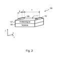
- the antiferromagnet may have an upper surface and the first and second contacts may be spaced apart and disposed on the upper surface.
- the memory device may comprise third and fourth additional electrodes to the antiferromagnet for measuring four-terminal ohmic resistance of the antiferromagnet.
- the memory device may further comprise a non-ferromagnetic layer interposed between the antiferromagnet and the insulator.
- the non-ferromagnetic layer may comprise a transition metal, such as platinum (Pt) or palladium (Pd).
- the non-ferromagnetic layer may be thin, for example, one or two monolayers thick.
- the first and second electrodes may be directly in contact with the antiferromagnet.
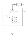
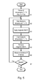
- a first, high resistance state R H and a second, low resistance state R H of the antiferromagnet 107 are obtained by cooling the device 106 in magnetic fields applied along the x- or y-directions.
- the enhanced susceptibility of the antiferromagnetic material when crossing the Néel temperature T N allows realization of different metastable antiferromagnetic configurations 112 1 , 112 2 .
Landscapes
- Engineering & Computer Science (AREA)
- Computer Hardware Design (AREA)
- Mram Or Spin Memory Techniques (AREA)
- Hall/Mr Elements (AREA)
- Semiconductor Memories (AREA)
Priority Applications (2)
| Application Number | Priority Date | Filing Date | Title |
|---|---|---|---|
| EP13196118.7A EP2882004B1 (de) | 2013-12-06 | 2013-12-06 | Speichervorrichtung basierend auf anisotropem Magnetowiderstand |
| JP2014181312A JP2015115603A (ja) | 2013-12-06 | 2014-09-05 | メモリ・デバイス |
Applications Claiming Priority (1)
| Application Number | Priority Date | Filing Date | Title |
|---|---|---|---|
| EP13196118.7A EP2882004B1 (de) | 2013-12-06 | 2013-12-06 | Speichervorrichtung basierend auf anisotropem Magnetowiderstand |
Publications (2)
| Publication Number | Publication Date |
|---|---|
| EP2882004A1 true EP2882004A1 (de) | 2015-06-10 |
| EP2882004B1 EP2882004B1 (de) | 2017-04-05 |
Family
ID=49709576
Family Applications (1)
| Application Number | Title | Priority Date | Filing Date |
|---|---|---|---|
| EP13196118.7A Not-in-force EP2882004B1 (de) | 2013-12-06 | 2013-12-06 | Speichervorrichtung basierend auf anisotropem Magnetowiderstand |
Country Status (2)
| Country | Link |
|---|---|
| EP (1) | EP2882004B1 (de) |
| JP (1) | JP2015115603A (de) |
Cited By (3)
| Publication number | Priority date | Publication date | Assignee | Title |
|---|---|---|---|---|
| WO2020018649A1 (en) | 2018-07-17 | 2020-01-23 | Carlisle Interconnect Technologies, Inc. | High speed electrical connector assembly |
| EP3828890A1 (de) * | 2019-11-26 | 2021-06-02 | Consejo Superior de Investigaciones Científicas (CSIC) | Antiferromagnetische biegbare aufzeichnungsvorrichtung |
| US11411171B2 (en) | 2018-08-07 | 2022-08-09 | Ip2Ipo Innovations Limited | Non-volatile memory cell |
Citations (2)
| Publication number | Priority date | Publication date | Assignee | Title |
|---|---|---|---|---|
| JP2007048388A (ja) * | 2005-08-10 | 2007-02-22 | Nippon Hoso Kyokai <Nhk> | 磁気ヘッドおよび磁気ヘッド作製方法、並びに、磁気記録再生装置 |
| EP2065886A1 (de) | 2007-11-27 | 2009-06-03 | Hitachi Ltd. | Magnetoresistive Vorrichtung |
-
2013
- 2013-12-06 EP EP13196118.7A patent/EP2882004B1/de not_active Not-in-force
-
2014
- 2014-09-05 JP JP2014181312A patent/JP2015115603A/ja active Pending
Patent Citations (2)
| Publication number | Priority date | Publication date | Assignee | Title |
|---|---|---|---|---|
| JP2007048388A (ja) * | 2005-08-10 | 2007-02-22 | Nippon Hoso Kyokai <Nhk> | 磁気ヘッドおよび磁気ヘッド作製方法、並びに、磁気記録再生装置 |
| EP2065886A1 (de) | 2007-11-27 | 2009-06-03 | Hitachi Ltd. | Magnetoresistive Vorrichtung |
Non-Patent Citations (4)
| Title |
|---|
| B. G. PARK ET AL.: "A spin-valve-like magnetoresistance of an antiferromagnet-based tunnel junction", NATURE MATERIALS, vol. 10, 2011, pages 347 - 351, XP055060585, DOI: doi:10.1038/nmat2983 |
| C. CHAPPERT; A. FERT; F. N. VAN DAU: "The emergence of spin electronics in data storage", NATURE MATERIALS, vol. 6, 2007, pages 813 - 823, XP055051858, DOI: doi:10.1038/nmat2024 |
| C. GOULD ET AL.: "Tunneling Anisotropic Magnetoresistance: A Spin-Valve-Like Tunnel Magnetoresistance Using a Single Magnetic Layer", PHYSICAL REVIEW LETTERS, vol. 93, 2004, pages 117203, XP002475020 |
| PETTI D ET AL: "Storing magnetic information in IrMn/MgO/Ta tunnel junctions via field-cooling", APPLIED PHYSICS LETTERS, AMERICAN INSTITUTE OF PHYSICS, US, vol. 102, no. 19, 13 May 2013 (2013-05-13), pages 192404 - 192404, XP012172966, ISSN: 0003-6951, [retrieved on 20130514], DOI: 10.1063/1.4804429 * |
Cited By (4)
| Publication number | Priority date | Publication date | Assignee | Title |
|---|---|---|---|---|
| WO2020018649A1 (en) | 2018-07-17 | 2020-01-23 | Carlisle Interconnect Technologies, Inc. | High speed electrical connector assembly |
| US11411171B2 (en) | 2018-08-07 | 2022-08-09 | Ip2Ipo Innovations Limited | Non-volatile memory cell |
| EP3828890A1 (de) * | 2019-11-26 | 2021-06-02 | Consejo Superior de Investigaciones Científicas (CSIC) | Antiferromagnetische biegbare aufzeichnungsvorrichtung |
| WO2021105113A1 (en) | 2019-11-26 | 2021-06-03 | Consejo Superior De Investigaciones Cientificas | An antiferromagnetic bendable recording device |
Also Published As
| Publication number | Publication date |
|---|---|
| EP2882004B1 (de) | 2017-04-05 |
| JP2015115603A (ja) | 2015-06-22 |
Similar Documents
| Publication | Publication Date | Title |
|---|---|---|
| US7929370B2 (en) | Spin momentum transfer MRAM design | |
| US7532504B2 (en) | Spin injection magnetic domain wall displacement device and element thereof | |
| US9576631B2 (en) | Spin hall effect magnetic apparatus, method and applications | |
| US9830966B2 (en) | Three terminal SOT memory cell with anomalous Hall effect | |
| EP3001470B1 (de) | Antiferromagnetische Speichervorrichtung | |
| JP4777613B2 (ja) | 磁気トンネル接合を有する磁気装置、メモリアレイ、及びこれらを用いた読み出し/書き込み方法 | |
| US9343658B2 (en) | Magnetic memory bits with perpendicular magnetization switched by current-induced spin-orbit torques | |
| USRE49364E1 (en) | Memory element, memory apparatus | |
| US7372116B2 (en) | Heat assisted switching in an MRAM cell utilizing the antiferromagnetic to ferromagnetic transition in FeRh | |
| US7532502B2 (en) | Spin injection magnetic domain wall displacement device and element thereof | |
| US20140103472A1 (en) | Inverted orthogonal spin transfer layer stack | |
| WO2013032492A1 (en) | Spin-transfer torque magnetic random access memory with perpendicular magnetic anisotropy multilayers | |
| US9082950B2 (en) | Increased magnetoresistance in an inverted orthogonal spin transfer layer stack | |
| WO2007126071A1 (ja) | 磁性薄膜及びそれを用いた磁気抵抗効果素子並びに磁気デバイス | |
| US20100128520A1 (en) | Non volatile memory including stabilizing structures | |
| KR20120046085A (ko) | 수직 이방성 및 향상층을 갖는 자기 터널 접합 셀들 | |
| US9053800B2 (en) | Memory element and memory apparatus | |
| US10302711B2 (en) | Spin hall effect magnetic structures | |
| CN107110921B (zh) | 具有改进的可编程性和灵敏度的基于mlu的磁性传感器 | |
| EP2882004B1 (de) | Speichervorrichtung basierend auf anisotropem Magnetowiderstand | |
| EP2744002B1 (de) | Speichervorrichtung | |
| KR20140135566A (ko) | 자기저항요소 및 이를 포함하는 메모리소자 | |
| JP2012074716A (ja) | 記憶素子及びメモリ | |
| EP3023803A1 (de) | MLU-Messzelle zur Abtastung eines externen Magnetfeldes und magnetische Sensorvorrichtung mit der MLU-Zelle | |
| US20250380616A1 (en) | Stt mram device with perpendicular exchange bias layer in contact with free layer |
Legal Events
| Date | Code | Title | Description |
|---|---|---|---|
| PUAI | Public reference made under article 153(3) epc to a published international application that has entered the european phase |
Free format text: ORIGINAL CODE: 0009012 |
|
| 17P | Request for examination filed |
Effective date: 20131206 |
|
| AK | Designated contracting states |
Kind code of ref document: A1 Designated state(s): AL AT BE BG CH CY CZ DE DK EE ES FI FR GB GR HR HU IE IS IT LI LT LU LV MC MK MT NL NO PL PT RO RS SE SI SK SM TR |
|
| AX | Request for extension of the european patent |
Extension state: BA ME |
|
| R17P | Request for examination filed (corrected) |
Effective date: 20151127 |
|
| RBV | Designated contracting states (corrected) |
Designated state(s): AL AT BE BG CH CY CZ DE DK EE ES FI FR GB GR HR HU IE IS IT LI LT LU LV MC MK MT NL NO PL PT RO RS SE SI SK SM TR |
|
| 17Q | First examination report despatched |
Effective date: 20160506 |
|
| GRAP | Despatch of communication of intention to grant a patent |
Free format text: ORIGINAL CODE: EPIDOSNIGR1 |
|
| STAA | Information on the status of an ep patent application or granted ep patent |
Free format text: STATUS: GRANT OF PATENT IS INTENDED |
|
| INTG | Intention to grant announced |
Effective date: 20161209 |
|
| GRAS | Grant fee paid |
Free format text: ORIGINAL CODE: EPIDOSNIGR3 |
|
| GRAA | (expected) grant |
Free format text: ORIGINAL CODE: 0009210 |
|
| STAA | Information on the status of an ep patent application or granted ep patent |
Free format text: STATUS: THE PATENT HAS BEEN GRANTED |
|
| AK | Designated contracting states |
Kind code of ref document: B1 Designated state(s): AL AT BE BG CH CY CZ DE DK EE ES FI FR GB GR HR HU IE IS IT LI LT LU LV MC MK MT NL NO PL PT RO RS SE SI SK SM TR |
|
| REG | Reference to a national code |
Ref country code: GB Ref legal event code: FG4D |
|
| REG | Reference to a national code |
Ref country code: CH Ref legal event code: EP |
|
| REG | Reference to a national code |
Ref country code: AT Ref legal event code: REF Ref document number: 882557 Country of ref document: AT Kind code of ref document: T Effective date: 20170415 |
|
| REG | Reference to a national code |
Ref country code: IE Ref legal event code: FG4D |
|
| REG | Reference to a national code |
Ref country code: DE Ref legal event code: R096 Ref document number: 602013019387 Country of ref document: DE |
|
| REG | Reference to a national code |
Ref country code: NL Ref legal event code: MP Effective date: 20170405 |
|
| REG | Reference to a national code |
Ref country code: LT Ref legal event code: MG4D |
|
| REG | Reference to a national code |
Ref country code: AT Ref legal event code: MK05 Ref document number: 882557 Country of ref document: AT Kind code of ref document: T Effective date: 20170405 |
|
| PG25 | Lapsed in a contracting state [announced via postgrant information from national office to epo] |
Ref country code: NL Free format text: LAPSE BECAUSE OF FAILURE TO SUBMIT A TRANSLATION OF THE DESCRIPTION OR TO PAY THE FEE WITHIN THE PRESCRIBED TIME-LIMIT Effective date: 20170405 |
|
| PG25 | Lapsed in a contracting state [announced via postgrant information from national office to epo] |
Ref country code: AT Free format text: LAPSE BECAUSE OF FAILURE TO SUBMIT A TRANSLATION OF THE DESCRIPTION OR TO PAY THE FEE WITHIN THE PRESCRIBED TIME-LIMIT Effective date: 20170405 Ref country code: LT Free format text: LAPSE BECAUSE OF FAILURE TO SUBMIT A TRANSLATION OF THE DESCRIPTION OR TO PAY THE FEE WITHIN THE PRESCRIBED TIME-LIMIT Effective date: 20170405 Ref country code: NO Free format text: LAPSE BECAUSE OF FAILURE TO SUBMIT A TRANSLATION OF THE DESCRIPTION OR TO PAY THE FEE WITHIN THE PRESCRIBED TIME-LIMIT Effective date: 20170705 Ref country code: GR Free format text: LAPSE BECAUSE OF FAILURE TO SUBMIT A TRANSLATION OF THE DESCRIPTION OR TO PAY THE FEE WITHIN THE PRESCRIBED TIME-LIMIT Effective date: 20170706 Ref country code: ES Free format text: LAPSE BECAUSE OF FAILURE TO SUBMIT A TRANSLATION OF THE DESCRIPTION OR TO PAY THE FEE WITHIN THE PRESCRIBED TIME-LIMIT Effective date: 20170405 Ref country code: HR Free format text: LAPSE BECAUSE OF FAILURE TO SUBMIT A TRANSLATION OF THE DESCRIPTION OR TO PAY THE FEE WITHIN THE PRESCRIBED TIME-LIMIT Effective date: 20170405 Ref country code: FI Free format text: LAPSE BECAUSE OF FAILURE TO SUBMIT A TRANSLATION OF THE DESCRIPTION OR TO PAY THE FEE WITHIN THE PRESCRIBED TIME-LIMIT Effective date: 20170405 |
|
| PG25 | Lapsed in a contracting state [announced via postgrant information from national office to epo] |
Ref country code: LV Free format text: LAPSE BECAUSE OF FAILURE TO SUBMIT A TRANSLATION OF THE DESCRIPTION OR TO PAY THE FEE WITHIN THE PRESCRIBED TIME-LIMIT Effective date: 20170405 Ref country code: RS Free format text: LAPSE BECAUSE OF FAILURE TO SUBMIT A TRANSLATION OF THE DESCRIPTION OR TO PAY THE FEE WITHIN THE PRESCRIBED TIME-LIMIT Effective date: 20170405 Ref country code: BG Free format text: LAPSE BECAUSE OF FAILURE TO SUBMIT A TRANSLATION OF THE DESCRIPTION OR TO PAY THE FEE WITHIN THE PRESCRIBED TIME-LIMIT Effective date: 20170705 Ref country code: IS Free format text: LAPSE BECAUSE OF FAILURE TO SUBMIT A TRANSLATION OF THE DESCRIPTION OR TO PAY THE FEE WITHIN THE PRESCRIBED TIME-LIMIT Effective date: 20170805 Ref country code: SE Free format text: LAPSE BECAUSE OF FAILURE TO SUBMIT A TRANSLATION OF THE DESCRIPTION OR TO PAY THE FEE WITHIN THE PRESCRIBED TIME-LIMIT Effective date: 20170405 Ref country code: PL Free format text: LAPSE BECAUSE OF FAILURE TO SUBMIT A TRANSLATION OF THE DESCRIPTION OR TO PAY THE FEE WITHIN THE PRESCRIBED TIME-LIMIT Effective date: 20170405 |
|
| REG | Reference to a national code |
Ref country code: DE Ref legal event code: R097 Ref document number: 602013019387 Country of ref document: DE |
|
| PG25 | Lapsed in a contracting state [announced via postgrant information from national office to epo] |
Ref country code: DK Free format text: LAPSE BECAUSE OF FAILURE TO SUBMIT A TRANSLATION OF THE DESCRIPTION OR TO PAY THE FEE WITHIN THE PRESCRIBED TIME-LIMIT Effective date: 20170405 Ref country code: CZ Free format text: LAPSE BECAUSE OF FAILURE TO SUBMIT A TRANSLATION OF THE DESCRIPTION OR TO PAY THE FEE WITHIN THE PRESCRIBED TIME-LIMIT Effective date: 20170405 Ref country code: SK Free format text: LAPSE BECAUSE OF FAILURE TO SUBMIT A TRANSLATION OF THE DESCRIPTION OR TO PAY THE FEE WITHIN THE PRESCRIBED TIME-LIMIT Effective date: 20170405 Ref country code: EE Free format text: LAPSE BECAUSE OF FAILURE TO SUBMIT A TRANSLATION OF THE DESCRIPTION OR TO PAY THE FEE WITHIN THE PRESCRIBED TIME-LIMIT Effective date: 20170405 Ref country code: RO Free format text: LAPSE BECAUSE OF FAILURE TO SUBMIT A TRANSLATION OF THE DESCRIPTION OR TO PAY THE FEE WITHIN THE PRESCRIBED TIME-LIMIT Effective date: 20170405 |
|
| PLBE | No opposition filed within time limit |
Free format text: ORIGINAL CODE: 0009261 |
|
| STAA | Information on the status of an ep patent application or granted ep patent |
Free format text: STATUS: NO OPPOSITION FILED WITHIN TIME LIMIT |
|
| PG25 | Lapsed in a contracting state [announced via postgrant information from national office to epo] |
Ref country code: SM Free format text: LAPSE BECAUSE OF FAILURE TO SUBMIT A TRANSLATION OF THE DESCRIPTION OR TO PAY THE FEE WITHIN THE PRESCRIBED TIME-LIMIT Effective date: 20170405 Ref country code: IT Free format text: LAPSE BECAUSE OF FAILURE TO SUBMIT A TRANSLATION OF THE DESCRIPTION OR TO PAY THE FEE WITHIN THE PRESCRIBED TIME-LIMIT Effective date: 20170405 |
|
| 26N | No opposition filed |
Effective date: 20180108 |
|
| PG25 | Lapsed in a contracting state [announced via postgrant information from national office to epo] |
Ref country code: SI Free format text: LAPSE BECAUSE OF FAILURE TO SUBMIT A TRANSLATION OF THE DESCRIPTION OR TO PAY THE FEE WITHIN THE PRESCRIBED TIME-LIMIT Effective date: 20170405 |
|
| REG | Reference to a national code |
Ref country code: CH Ref legal event code: PL |
|
| REG | Reference to a national code |
Ref country code: IE Ref legal event code: MM4A |
|
| PG25 | Lapsed in a contracting state [announced via postgrant information from national office to epo] |
Ref country code: LU Free format text: LAPSE BECAUSE OF NON-PAYMENT OF DUE FEES Effective date: 20171206 Ref country code: MT Free format text: LAPSE BECAUSE OF NON-PAYMENT OF DUE FEES Effective date: 20171206 |
|
| REG | Reference to a national code |
Ref country code: FR Ref legal event code: ST Effective date: 20180831 |
|
| REG | Reference to a national code |
Ref country code: BE Ref legal event code: MM Effective date: 20171231 |
|
| PG25 | Lapsed in a contracting state [announced via postgrant information from national office to epo] |
Ref country code: FR Free format text: LAPSE BECAUSE OF NON-PAYMENT OF DUE FEES Effective date: 20180102 Ref country code: IE Free format text: LAPSE BECAUSE OF NON-PAYMENT OF DUE FEES Effective date: 20171206 |
|
| PG25 | Lapsed in a contracting state [announced via postgrant information from national office to epo] |
Ref country code: CH Free format text: LAPSE BECAUSE OF NON-PAYMENT OF DUE FEES Effective date: 20171231 Ref country code: LI Free format text: LAPSE BECAUSE OF NON-PAYMENT OF DUE FEES Effective date: 20171231 Ref country code: BE Free format text: LAPSE BECAUSE OF NON-PAYMENT OF DUE FEES Effective date: 20171231 |
|
| PG25 | Lapsed in a contracting state [announced via postgrant information from national office to epo] |
Ref country code: HU Free format text: LAPSE BECAUSE OF FAILURE TO SUBMIT A TRANSLATION OF THE DESCRIPTION OR TO PAY THE FEE WITHIN THE PRESCRIBED TIME-LIMIT; INVALID AB INITIO Effective date: 20131206 Ref country code: MC Free format text: LAPSE BECAUSE OF FAILURE TO SUBMIT A TRANSLATION OF THE DESCRIPTION OR TO PAY THE FEE WITHIN THE PRESCRIBED TIME-LIMIT Effective date: 20170405 |
|
| PG25 | Lapsed in a contracting state [announced via postgrant information from national office to epo] |
Ref country code: CY Free format text: LAPSE BECAUSE OF FAILURE TO SUBMIT A TRANSLATION OF THE DESCRIPTION OR TO PAY THE FEE WITHIN THE PRESCRIBED TIME-LIMIT Effective date: 20170405 |
|
| PG25 | Lapsed in a contracting state [announced via postgrant information from national office to epo] |
Ref country code: MK Free format text: LAPSE BECAUSE OF FAILURE TO SUBMIT A TRANSLATION OF THE DESCRIPTION OR TO PAY THE FEE WITHIN THE PRESCRIBED TIME-LIMIT Effective date: 20170405 |
|
| PG25 | Lapsed in a contracting state [announced via postgrant information from national office to epo] |
Ref country code: TR Free format text: LAPSE BECAUSE OF FAILURE TO SUBMIT A TRANSLATION OF THE DESCRIPTION OR TO PAY THE FEE WITHIN THE PRESCRIBED TIME-LIMIT Effective date: 20170405 |
|
| PG25 | Lapsed in a contracting state [announced via postgrant information from national office to epo] |
Ref country code: PT Free format text: LAPSE BECAUSE OF FAILURE TO SUBMIT A TRANSLATION OF THE DESCRIPTION OR TO PAY THE FEE WITHIN THE PRESCRIBED TIME-LIMIT Effective date: 20170405 |
|
| PG25 | Lapsed in a contracting state [announced via postgrant information from national office to epo] |
Ref country code: AL Free format text: LAPSE BECAUSE OF FAILURE TO SUBMIT A TRANSLATION OF THE DESCRIPTION OR TO PAY THE FEE WITHIN THE PRESCRIBED TIME-LIMIT Effective date: 20170405 |
|
| REG | Reference to a national code |
Ref country code: DE Ref legal event code: R082 Ref document number: 602013019387 Country of ref document: DE Representative=s name: VENNER SHIPLEY LLP, DE |
|
| PGFP | Annual fee paid to national office [announced via postgrant information from national office to epo] |
Ref country code: DE Payment date: 20201124 Year of fee payment: 8 Ref country code: GB Payment date: 20201126 Year of fee payment: 8 |
|
| REG | Reference to a national code |
Ref country code: DE Ref legal event code: R119 Ref document number: 602013019387 Country of ref document: DE |
|
| GBPC | Gb: european patent ceased through non-payment of renewal fee |
Effective date: 20211206 |
|
| PG25 | Lapsed in a contracting state [announced via postgrant information from national office to epo] |
Ref country code: GB Free format text: LAPSE BECAUSE OF NON-PAYMENT OF DUE FEES Effective date: 20211206 Ref country code: DE Free format text: LAPSE BECAUSE OF NON-PAYMENT OF DUE FEES Effective date: 20220701 |