EP2881753A1 - Optical sensor arrangement and method of producing an optical sensor arrangement - Google Patents
Optical sensor arrangement and method of producing an optical sensor arrangement Download PDFInfo
- Publication number
- EP2881753A1 EP2881753A1 EP13199086.3A EP13199086A EP2881753A1 EP 2881753 A1 EP2881753 A1 EP 2881753A1 EP 13199086 A EP13199086 A EP 13199086A EP 2881753 A1 EP2881753 A1 EP 2881753A1
- Authority
- EP
- European Patent Office
- Prior art keywords
- light
- layer
- sensor arrangement
- detector
- optical sensor
- Prior art date
- Legal status (The legal status is an assumption and is not a legal conclusion. Google has not performed a legal analysis and makes no representation as to the accuracy of the status listed.)
- Granted
Links
Images

Classifications
-
- G—PHYSICS
- G01—MEASURING; TESTING
- G01S—RADIO DIRECTION-FINDING; RADIO NAVIGATION; DETERMINING DISTANCE OR VELOCITY BY USE OF RADIO WAVES; LOCATING OR PRESENCE-DETECTING BY USE OF THE REFLECTION OR RERADIATION OF RADIO WAVES; ANALOGOUS ARRANGEMENTS USING OTHER WAVES
- G01S7/00—Details of systems according to groups G01S13/00, G01S15/00, G01S17/00
- G01S7/48—Details of systems according to groups G01S13/00, G01S15/00, G01S17/00 of systems according to group G01S17/00
- G01S7/481—Constructional features, e.g. arrangements of optical elements
- G01S7/4811—Constructional features, e.g. arrangements of optical elements common to transmitter and receiver
- G01S7/4813—Housing arrangements
-
- G—PHYSICS
- G01—MEASURING; TESTING
- G01S—RADIO DIRECTION-FINDING; RADIO NAVIGATION; DETERMINING DISTANCE OR VELOCITY BY USE OF RADIO WAVES; LOCATING OR PRESENCE-DETECTING BY USE OF THE REFLECTION OR RERADIATION OF RADIO WAVES; ANALOGOUS ARRANGEMENTS USING OTHER WAVES
- G01S17/00—Systems using the reflection or reradiation of electromagnetic waves other than radio waves, e.g. lidar systems
- G01S17/02—Systems using the reflection of electromagnetic waves other than radio waves
- G01S17/04—Systems determining the presence of a target
-
- H—ELECTRICITY
- H10—SEMICONDUCTOR DEVICES; ELECTRIC SOLID-STATE DEVICES NOT OTHERWISE PROVIDED FOR
- H10F—INORGANIC SEMICONDUCTOR DEVICES SENSITIVE TO INFRARED RADIATION, LIGHT, ELECTROMAGNETIC RADIATION OF SHORTER WAVELENGTH OR CORPUSCULAR RADIATION
- H10F39/00—Integrated devices, or assemblies of multiple devices, comprising at least one element covered by group H10F30/00, e.g. radiation detectors comprising photodiode arrays
- H10F39/10—Integrated devices
- H10F39/103—Integrated devices the at least one element covered by H10F30/00 having potential barriers, e.g. integrated devices comprising photodiodes or phototransistors
-
- H—ELECTRICITY
- H10—SEMICONDUCTOR DEVICES; ELECTRIC SOLID-STATE DEVICES NOT OTHERWISE PROVIDED FOR
- H10F—INORGANIC SEMICONDUCTOR DEVICES SENSITIVE TO INFRARED RADIATION, LIGHT, ELECTROMAGNETIC RADIATION OF SHORTER WAVELENGTH OR CORPUSCULAR RADIATION
- H10F55/00—Radiation-sensitive semiconductor devices covered by groups H10F10/00, H10F19/00 or H10F30/00 being structurally associated with electric light sources and electrically or optically coupled thereto
- H10F55/10—Radiation-sensitive semiconductor devices covered by groups H10F10/00, H10F19/00 or H10F30/00 being structurally associated with electric light sources and electrically or optically coupled thereto wherein the radiation-sensitive semiconductor devices control the electric light source, e.g. image converters, image amplifiers or image storage devices
-
- H—ELECTRICITY
- H10—SEMICONDUCTOR DEVICES; ELECTRIC SOLID-STATE DEVICES NOT OTHERWISE PROVIDED FOR
- H10F—INORGANIC SEMICONDUCTOR DEVICES SENSITIVE TO INFRARED RADIATION, LIGHT, ELECTROMAGNETIC RADIATION OF SHORTER WAVELENGTH OR CORPUSCULAR RADIATION
- H10F55/00—Radiation-sensitive semiconductor devices covered by groups H10F10/00, H10F19/00 or H10F30/00 being structurally associated with electric light sources and electrically or optically coupled thereto
- H10F55/18—Radiation-sensitive semiconductor devices covered by groups H10F10/00, H10F19/00 or H10F30/00 being structurally associated with electric light sources and electrically or optically coupled thereto wherein the radiation-sensitive semiconductor devices and the electric light source share a common body having dual-functionality of light emission and light detection
-
- H—ELECTRICITY
- H10—SEMICONDUCTOR DEVICES; ELECTRIC SOLID-STATE DEVICES NOT OTHERWISE PROVIDED FOR
- H10F—INORGANIC SEMICONDUCTOR DEVICES SENSITIVE TO INFRARED RADIATION, LIGHT, ELECTROMAGNETIC RADIATION OF SHORTER WAVELENGTH OR CORPUSCULAR RADIATION
- H10F55/00—Radiation-sensitive semiconductor devices covered by groups H10F10/00, H10F19/00 or H10F30/00 being structurally associated with electric light sources and electrically or optically coupled thereto
- H10F55/20—Radiation-sensitive semiconductor devices covered by groups H10F10/00, H10F19/00 or H10F30/00 being structurally associated with electric light sources and electrically or optically coupled thereto wherein the electric light source controls the radiation-sensitive semiconductor devices, e.g. optocouplers
- H10F55/25—Radiation-sensitive semiconductor devices covered by groups H10F10/00, H10F19/00 or H10F30/00 being structurally associated with electric light sources and electrically or optically coupled thereto wherein the electric light source controls the radiation-sensitive semiconductor devices, e.g. optocouplers wherein the radiation-sensitive devices and the electric light source are all semiconductor devices
-
- H—ELECTRICITY
- H10—SEMICONDUCTOR DEVICES; ELECTRIC SOLID-STATE DEVICES NOT OTHERWISE PROVIDED FOR
- H10F—INORGANIC SEMICONDUCTOR DEVICES SENSITIVE TO INFRARED RADIATION, LIGHT, ELECTROMAGNETIC RADIATION OF SHORTER WAVELENGTH OR CORPUSCULAR RADIATION
- H10F55/00—Radiation-sensitive semiconductor devices covered by groups H10F10/00, H10F19/00 or H10F30/00 being structurally associated with electric light sources and electrically or optically coupled thereto
- H10F55/20—Radiation-sensitive semiconductor devices covered by groups H10F10/00, H10F19/00 or H10F30/00 being structurally associated with electric light sources and electrically or optically coupled thereto wherein the electric light source controls the radiation-sensitive semiconductor devices, e.g. optocouplers
- H10F55/25—Radiation-sensitive semiconductor devices covered by groups H10F10/00, H10F19/00 or H10F30/00 being structurally associated with electric light sources and electrically or optically coupled thereto wherein the electric light source controls the radiation-sensitive semiconductor devices, e.g. optocouplers wherein the radiation-sensitive devices and the electric light source are all semiconductor devices
- H10F55/255—Radiation-sensitive semiconductor devices covered by groups H10F10/00, H10F19/00 or H10F30/00 being structurally associated with electric light sources and electrically or optically coupled thereto wherein the electric light source controls the radiation-sensitive semiconductor devices, e.g. optocouplers wherein the radiation-sensitive devices and the electric light source are all semiconductor devices formed in, or on, a common substrate
-
- H—ELECTRICITY
- H10—SEMICONDUCTOR DEVICES; ELECTRIC SOLID-STATE DEVICES NOT OTHERWISE PROVIDED FOR
- H10F—INORGANIC SEMICONDUCTOR DEVICES SENSITIVE TO INFRARED RADIATION, LIGHT, ELECTROMAGNETIC RADIATION OF SHORTER WAVELENGTH OR CORPUSCULAR RADIATION
- H10F77/00—Constructional details of devices covered by this subclass
- H10F77/30—Coatings
- H10F77/306—Coatings for devices having potential barriers
- H10F77/331—Coatings for devices having potential barriers for filtering or shielding light, e.g. multicolour filters for photodetectors
- H10F77/334—Coatings for devices having potential barriers for filtering or shielding light, e.g. multicolour filters for photodetectors for shielding light, e.g. light blocking layers or cold shields for infrared detectors
-
- H—ELECTRICITY
- H10—SEMICONDUCTOR DEVICES; ELECTRIC SOLID-STATE DEVICES NOT OTHERWISE PROVIDED FOR
- H10F—INORGANIC SEMICONDUCTOR DEVICES SENSITIVE TO INFRARED RADIATION, LIGHT, ELECTROMAGNETIC RADIATION OF SHORTER WAVELENGTH OR CORPUSCULAR RADIATION
- H10F77/00—Constructional details of devices covered by this subclass
- H10F77/30—Coatings
- H10F77/306—Coatings for devices having potential barriers
- H10F77/331—Coatings for devices having potential barriers for filtering or shielding light, e.g. multicolour filters for photodetectors
- H10F77/337—Coatings for devices having potential barriers for filtering or shielding light, e.g. multicolour filters for photodetectors using interference filters, e.g. multilayer dielectric filters
-
- H—ELECTRICITY
- H10—SEMICONDUCTOR DEVICES; ELECTRIC SOLID-STATE DEVICES NOT OTHERWISE PROVIDED FOR
- H10F—INORGANIC SEMICONDUCTOR DEVICES SENSITIVE TO INFRARED RADIATION, LIGHT, ELECTROMAGNETIC RADIATION OF SHORTER WAVELENGTH OR CORPUSCULAR RADIATION
- H10F77/00—Constructional details of devices covered by this subclass
- H10F77/40—Optical elements or arrangements
- H10F77/407—Optical elements or arrangements indirectly associated with the devices
-
- H—ELECTRICITY
- H10—SEMICONDUCTOR DEVICES; ELECTRIC SOLID-STATE DEVICES NOT OTHERWISE PROVIDED FOR
- H10F—INORGANIC SEMICONDUCTOR DEVICES SENSITIVE TO INFRARED RADIATION, LIGHT, ELECTROMAGNETIC RADIATION OF SHORTER WAVELENGTH OR CORPUSCULAR RADIATION
- H10F77/00—Constructional details of devices covered by this subclass
- H10F77/40—Optical elements or arrangements
- H10F77/413—Optical elements or arrangements directly associated or integrated with the devices, e.g. back reflectors
-
- H—ELECTRICITY
- H10—SEMICONDUCTOR DEVICES; ELECTRIC SOLID-STATE DEVICES NOT OTHERWISE PROVIDED FOR
- H10F—INORGANIC SEMICONDUCTOR DEVICES SENSITIVE TO INFRARED RADIATION, LIGHT, ELECTROMAGNETIC RADIATION OF SHORTER WAVELENGTH OR CORPUSCULAR RADIATION
- H10F77/00—Constructional details of devices covered by this subclass
- H10F77/50—Encapsulations or containers
-
- H—ELECTRICITY
- H10—SEMICONDUCTOR DEVICES; ELECTRIC SOLID-STATE DEVICES NOT OTHERWISE PROVIDED FOR
- H10F—INORGANIC SEMICONDUCTOR DEVICES SENSITIVE TO INFRARED RADIATION, LIGHT, ELECTROMAGNETIC RADIATION OF SHORTER WAVELENGTH OR CORPUSCULAR RADIATION
- H10F77/00—Constructional details of devices covered by this subclass
- H10F77/93—Interconnections
- H10F77/933—Interconnections for devices having potential barriers
-
- H—ELECTRICITY
- H10—SEMICONDUCTOR DEVICES; ELECTRIC SOLID-STATE DEVICES NOT OTHERWISE PROVIDED FOR
- H10H—INORGANIC LIGHT-EMITTING SEMICONDUCTOR DEVICES HAVING POTENTIAL BARRIERS
- H10H20/00—Individual inorganic light-emitting semiconductor devices having potential barriers, e.g. light-emitting diodes [LED]
- H10H20/80—Constructional details
- H10H20/85—Packages
- H10H20/8506—Containers
-
- H—ELECTRICITY
- H10—SEMICONDUCTOR DEVICES; ELECTRIC SOLID-STATE DEVICES NOT OTHERWISE PROVIDED FOR
- H10H—INORGANIC LIGHT-EMITTING SEMICONDUCTOR DEVICES HAVING POTENTIAL BARRIERS
- H10H20/00—Individual inorganic light-emitting semiconductor devices having potential barriers, e.g. light-emitting diodes [LED]
- H10H20/80—Constructional details
- H10H20/85—Packages
- H10H20/852—Encapsulations
-
- H—ELECTRICITY
- H10—SEMICONDUCTOR DEVICES; ELECTRIC SOLID-STATE DEVICES NOT OTHERWISE PROVIDED FOR
- H10W—GENERIC PACKAGES, INTERCONNECTIONS, CONNECTORS OR OTHER CONSTRUCTIONAL DETAILS OF DEVICES COVERED BY CLASS H10
- H10W90/00—Package configurations
-
- H—ELECTRICITY
- H10—SEMICONDUCTOR DEVICES; ELECTRIC SOLID-STATE DEVICES NOT OTHERWISE PROVIDED FOR
- H10W—GENERIC PACKAGES, INTERCONNECTIONS, CONNECTORS OR OTHER CONSTRUCTIONAL DETAILS OF DEVICES COVERED BY CLASS H10
- H10W72/00—Interconnections or connectors in packages
- H10W72/071—Connecting or disconnecting
- H10W72/072—Connecting or disconnecting of bump connectors
- H10W72/07251—Connecting or disconnecting of bump connectors characterised by changes in properties of the bump connectors during connecting
-
- H—ELECTRICITY
- H10—SEMICONDUCTOR DEVICES; ELECTRIC SOLID-STATE DEVICES NOT OTHERWISE PROVIDED FOR
- H10W—GENERIC PACKAGES, INTERCONNECTIONS, CONNECTORS OR OTHER CONSTRUCTIONAL DETAILS OF DEVICES COVERED BY CLASS H10
- H10W72/00—Interconnections or connectors in packages
- H10W72/20—Bump connectors, e.g. solder bumps or copper pillars; Dummy bumps; Thermal bumps
Definitions
- This invention relates to an optical sensor arrangement and a method of producing an optical sensor arrangement.
- the invention relates to an optical proximity sensor arrangement and a method of producing an optical proximity sensor arrangement.
- An optical proximity sensor is a sensor able to detect the presence of nearby objects by means of electromagnetic radiation without any physical contact.
- a proximity sensor emits a continuous or pulsed electromagnetic field, e.g. infrared, and detects changes in the field or return signal.
- the term "optical” in this respect relates to the infrared, visible and ultraviolet part of the electromagnetic spectrum.
- optical proximity sensors are realized with multi-chip packages based on printed circuit boards (PCB) which are over-molded by common molding techniques. These packages, however, are bulky and have rather big footprint.
- PCB printed circuit boards
- PDA personal digital assistants
- laptops With such devices there is a strong need to reduce size and increase functionality per area.
- An optical sensor arrangement in particular an optical proximity sensor arrangement, comprises a three-dimensional integrated circuit.
- the three-dimensional integrated circuit further comprises a first layer, a second layer and a mold layer.
- the first layer comprises a light-emitting device.
- the second layer comprises a light detector and a driver circuit.
- the driver circuit is electrically connected to the light-emitting device and to the light-detector.
- the mold layer further comprises a first light barrier between the light-emitting device and the light-detector. The first light barrier is configured to block light from transmitting directly from the light-emitting device to the light-detector.
- the light-emitting device can be a light emitting diode emitting visible light or infrared light.
- the term "light” denotes electromagnetic radiation in the infrared (IR), visible and ultraviolet (UV) spectrum.
- IR infrared
- UV ultraviolet
- infrared light emitting diodes are used with the optical sensor arrangement. These can be produced at low cost and emit light not visible to the human eye.
- the light-detector can be a photo-diode, charge coupled device (CCD) or complementary metal oxide semiconductor (CMOS) type light detector.
- CCD charge coupled device
- CMOS complementary metal oxide semiconductor
- the light-emitting device emits light, either continuously or in a pulsed fashion. Due to the first light barrier in the mold layer the light-detector detects light emitted from the light-emitting device only if it gets reflected by a proximity object, i.e. the first light barrier blocks light from being transmitted directly from the light-emitting device to the light-detector. However, the light-detector is typically also exposed to ambient light from the surroundings of the optical sensor arrangement. To account for this contribution the control device can optionally be configured to record the amount of ambient light and correct for it. For example, this can be achieved by letting the light-emitting device emit pulses of a certain duration. During the pauses when no light is emitted the light-detector only detects ambient light.
- the sensor Due to the three-dimensional integration of the optical sensor arrangement the sensor can be packaged into a rather small volume as compared to multichip packages. This results in a rather small footprint as the respective layer can be heterogeneously stacked and/or embedded.
- the mold layer By means of the mold layer, the overall layout of the sensor arrangement can be largely adapted and its optical properties can be fine-tuned.
- the proposed design leads to rather low heights when compared to multichip packages.
- the optical sensor arrangement can be produced with few process steps and at reduced cost.
- the mold layer effectively protects or seals the optical sensor arrangement from environmental influences. Furthermore, the mold layer provides a shield from unwanted ambient light, for instance, infrared radiation which does not originate from the light-emitting device.
- 3D-IC three-dimensional integrated circuit
- layer relates to the structure into which a circuit can be integrated, for example a substrate.
- molding refers to the process of shaping a mold structure from a raw mold material using a rigid frame or model, called a pattern.
- the mold layer comprises an optically opaque mold material.
- the term "opaque” describes a material property of the mold material so that the mold layer is neither transparent not allowing any light to pass through nor translucent allowing some light to pass through.
- One preferred mold material is plastics.
- the mold layer comprises a wafer level mold structure.
- the wafer level mold structure is produced at a wafer level by using molding, in particular transfer molding techniques,such as film-assisted molding, for instance.
- film-assisted molding uses a plastic film which is attached to an inner surfaces of the mold by vacuum before a layer like the first and second layer, i.e. the products to be encapsulated, are loaded into the mold. Then, the mold is closed, effectively leaving a cavity in the (inverse) shape of the mold layer to be produced. Finally, the cavity is filled with liquid mold material and, after the mold material has cured, the mold layer has taken the shape forced by the mold, e.g. the first light barrier is designed into the mold layer.
- the mold layer is at least partially connected to a main surface of the second layer.
- the mold layer comprises a first aperture to which the first layer is attached.
- the first aperture is attached to the first layer in such a way that light from the light-emitting device can be emitted through the first aperture.
- the first aperture establishes an optical path for emission of light by the light-emitting device.
- the aperture in the mold layer blocks light from reaching the light-detector directly.
- the mold layer comprises a second aperture to which the light-detector is attached.
- the second aperture assures that light can be detected by means of the light-detector. This way the mold layer can be extended along the main surface of the second layer.
- the second aperture assures that light can reach the light-detector while blocking direct transmission from the light-emitting device.
- the second layer comprises a substrate into which the light-detector and the control circuit are integrated.
- the control circuit and the light-detector can be realized with a single chip which further reduces the footprint of the optical sensor arrangement.
- the control circuit and the light-detector can be integrated into a recess formed in the substrate. Electrical connections can be designed into the substrate with known techniques.
- the substrate comprises an active interposer.
- the active interposer may be further connected to a redistribution layer or an embedded wafer level wall grid array.
- the interposer is an electrical interface routing between one socket and connection of the electronic circuits to another.
- a redistribution layer is a metal layer on a layer that makes the input/output pads of the integrated circuit available at other locations along the layer.
- the embedded wafer level ball grid array (eWLB) is the result of a packaging technology for integrated circuits interconnecting pads of an integrated circuit. When an integrated circuit is manufactured it usually has a set of Input / Output pads that are area wire bonded to pins of the package.
- By means of the interposer an extra layer of wiring on the chip is provided enabling bonding out from different locations on the chip making chip-to-chip bonding simpler.
- the light-emitting device is electrically connected to the second layer by means of a metallization structured topology, a bond wire or a redistribution layer.
- the metallization structured topology comprises a structured metallization and provides electrical connectivity between the first and second layer.
- the first layer is stacked onto the main surface of the second layer.
- the first layer is embedded into a recess formed in the second layer.
- the first layer is stacked onto a further main surface of the second layer opposite to the main surface. In this case the first aperture extends through the second layer.
- the second layer comprises a second light barrier. While the first light barrier is designed to block light from being directly transmitted to the light detector via the mold layer the second light barrier has a similar purpose. It effectively blocks light from being directly transmitted to the light detector via the second layer.
- the material of the second layer could eventually not be completely opaque to the light emitted by the light detector.
- silicon is transparent to infrared to some extent.
- the second light barrier effectively reduces the amount of light reaching the light detector via the second layer material.
- the second light barrier comprises through-silicon vias designed into the substrate.
- a through-silicon via, or TSV for short is an electrical connection, via (Vertical Interconnect Access), passing completely through a silicon wafer or die.
- the second layer in this case comprises a silicon wafer or die.
- the electrical path of the TSV features absorbance of light, in particular infrared, to a high extent.
- the light-detector and/or light-emitting device are covered by an optical element.
- the optical element is a lens and/or zone plate.
- the lens can be a nano-imprinted lens.
- a method of producing an optical sensor arrangement comprises the step of integrating a light-emitting device into a first layer.
- a light-detector and a driver circuit are integrated into a second layer.
- the light-emitting device and the light-detector are then electrically connected.
- the method further comprises molding a mold layer comprising a first light barrier between the light-emitting device and the light-detector. Said mold layer is configured to block light from being transmitted directly from the light-emitting device to the light-detector.
- the first layer, the second layer and the mold layer are integrated into a three-dimensional integrated circuit.
- the sensor Due to the three-dimensional integration of the optical sensor arrangement the sensor can be packaged into a rather small volume as compared to multichip packages. This results in a rather small footprint as the respective layer can be heterogeneously stacked and/or embedded.
- the mold layer By means of the mold layer, the overall layout of the sensor arrangement can be largely adapted and its optical properties can be fine-tuned.
- the proposed design leads to rather low heights when compared to multichip packages.
- the optical sensor arrangement can be produced with few process steps and at reduced cost.
- the mold layer effectively protects or seals the optical sensor arrangement from environmental influences. Furthermore, the mold layer provides a shield from unwanted ambient light, for instance, infrared radiation which does not originate from the light-emitting device.
- the molding involves wafer-level molding, in particular wafer-level molding using an optically opaque material.
- Wafer-level molding involves molding at a wafer level, for example transfer molding techniques, such as film-assisted molding.
- the first layer is stacked onto the second layer, in particular stacked by means of die-to-wafer stacking.
- the first layer is then electrically connected to the second layer by means of a metallization structured topology, a bond wire or a redistribution layer, in particular by means of a metallization structured topology based on through-silicon vias.
- the first layer is embedded into a recess formed on the second layer.
- the mold layer is connected, at least partially, to a main surface of the second layer.
- a first aperture is provided in the mold layer to which the first layer is attached such that light from the light-emitting device can be emitted through the first aperture.
- a second aperture can be provided to which the light-detector is attached such that light can be detected by means of the light-detector.
- the first layer 1 comprises a light-emitting device LED which, preferably, is a light-emitting diode.
- the light-emitting diode emits visible light but in the field of optical proximity sensors emission of (near) infrared light is preferred.
- IR diodes are both cheap and emit light that is not visible to the human eye. The latter is a beneficial aspect from a design point of view as optical proximity sensors typically reside behind a dark cover. If said cover is optically opaque to visible light but transparent to IR, the structure and circuitry are invisible to users and, thus, do not interfere with smartphone design, for instance.
- the second layer 2 comprises a silicon substrate and has a main surface 23 and a further main surface 24 opposite to the main surface 23.
- the second layer 2 comprises a light-detector PD and a driver circuit IC.
- the light-detector PD and the driver circuit IC are integrated into the second layer 2.
- both components, LED, IC could be integrated into separate integrated circuits and connected to each other.
- the term "second layer" is used to cover both ways of integration.
- the light-detector PD comprises a photo-diode which is sensitive to light to be emitted from the light-emitting device LED.
- the photo-diode is sensitive to (near) infrared light.
- the light-detector PD may be a charge coupled device (CCD) or a CMOS light sensor. Typically, the latter devices are or can be manufactured to be sensitive to infrared.
- the driver circuit IC comprises means to control and operate both the light-detector PD and the light-emitting device LED.
- the second layer 2 comprises electrical connections between the driver circuit IC and both light-detector PD and the light-emitting device LED.
- the first layer 1 provides connection pads to the second layer 2 to allow the light emitting device LED to be operated.
- the connection to the second layer 2 is established through a metallization structured topology 11 which will be discussed in more detail with respect to Figures 7 to 9 .
- the first layer 1, comprising the light emitting device LED is bonded onto the second layer 2.
- the electrical connection is realized via the metallization structured topology 11 which connects the light-emitting device LED to the through-silicon via (TSV) connections 21.
- TSV through-silicon via
- the metallization structured topology 11 is produced by means of high topology lithography, like EVG Nano spray lithography, and further by spray-coating or sputtering of a metal layer.
- the second layer 2 constitutes an active interposer.
- the further main surface 24 comprises a redistribution layer or, alternatively, or may be connected to an embedded wafer level ball grid array, in order to make input/output pads available at locations of the optical sensor arrangement.
- This concerns electrical connections within the optical sensor arrangement e.g. between the light-emitting device LED, the driver circuit IC and the light detector PD, as well as connections to further external circuits in a system into which the optical sensor arrangement is embedded, for example, a smartphone, mobile phone or mobile computer. Connections to such other circuits are established via bumps 25, located at the further main surface 24.
- the mold layer 3 covers a stack of first and second layer 1, 2. Furthermore, the mold layer 3 has a characteristic shape which basically defines the optical paths within the optical sensor arrangement. The specifics of the mold shape is determined by the field of application of the optical sensor arrangement, e.g. optical proximity detection.
- the stack of first and second layer 1, 2 and mold layer 3 make up a three-dimensional integrated circuit.
- the mold layer 3 constitutes a wafer level mold structure which is produced at a wafer level by using molding techniques like transfer molding such as film-assisted molding. This way typically more than one optical sensor arrangement is produced at a time and individual ones are cut out by sawing.
- the shape of a mold determines the structure of the mold layer 3.
- film-assisted molding for example, a plastic film which is attached to an inner surface of the mold by vacuum before the first and second layer 1, 2, i.e. the products to be encapsulated, are loaded into the mold. Then the mold is closed, effectively leaving a cavity of the (inverse) shape of the mold layer 3 to be produced. Finally, the cavity is filled with liquid mold material and, after the mold material has cured, the mold layer 3 has taken the shape forced by the mold.
- the mold is structured so that it shapes the mold layer 3 to allow light emitted from the light-emitting device LED to leave the arrangement. At the same time it allows light to enter the arrangement and be detected by the light-detector PD.
- This functionality is implemented by means of a first and second aperture 31, 32 in the mold layer 3, respectively.
- the light-emitting device LED and the light-detector PD are placed in front of the first and second aperture 31, 32, respectively.
- a first light barrier 33 is designed into the mold layer 3 which resides between light-emitting device LED and the light-detector PD to block light from being transmitted directly between these two components.
- the first light barrier 33 is framed by the first and second apertures 31, 32.
- the mold layer 3 comprises an optically opaque material so that no light can pass the first light barrier 33.
- One preferred material is plastics.
- the second layer 2 comprises one or more second light barriers 22.
- this second light barrier 22 comprises through silicon vias in the shape of rectangles or rings around the light-emitting device LED and/or the light detector PD. This way, light emitted from the light-emitting device LED is blocked from reaching the light detector PD by way through the material of the second layer 2.
- the second layer 2 is typically made of silicon substrate which to some degree is transparent to light, in particular infrared light. The second light barrier 22 thus further reduces optical crosstalk.
- the optical sensor arrangement can be covered by the cover layer 4.
- the cover layer 4 comprises a transparent or at least translucent mold material and seals the optical sensor arrangement of its surroundings.
- mold material can also fill the first and/or second aperture 31, 32.
- Part of the cover can be in the form of optical elements 41, which may have the shape of an optical lens and/or a zone plate like a Fresnel lens. Examples are discussed with respect to further embodiments and can be used with the present embodiment of Figure 1A as well.
- optical elements 41 e.g. lenses
- the lenses reside inside the first and second aperture 31, 32, respectively.
- the lenses serve as optical elements 41 shaping beams of light emitted by the light-emitting device LED and/or detected by the light detector PD to improve signal-to-noise ratio and reduce optical cross-talk.
- FIG. 1C The embodiment shown in Figure 1C is based on that of Figure 1C .
- the lenses 41 reside on top of the first and second aperture 31, 32, thereby sealing the optical sensor arrangement from its environment.
- Figure 2 shows another embodiment of the optical sensor arrangement. This embodiment is based on the ones disclosed in Figures 1A to 1C and only differs in the connection of the first layer 1 to the second layer 2.
- the first layer 1 resides in a cavity which is etched into the second layer 2 in order to have the same surface height as the first layer 1.
- the light-emitting device LED is bonded into the cavity and electrically connected by means of a low topology lithography for metal contact as discussed above.
- the optical elements can be provided in the way discussed with respect to Figures 1A to 1C .
- Figure 3 shows another embodiment of the optical sensor arrangement. This embodiment is based on the ones disclosed in Figures 1A to 1C but differs in the way the first layer 1 is connected to the second layer 2.
- the first aperture 31 is cut through the second layer 2 and the mold layer 3 completely leaving a hole 34.
- the additional hole 34 in the second layer 2 is e.g. formed by a wide diameter TSV and a diffractive RIE etch before or after wafer level molding selective to the mold compound.
- the first layer 1 is connected to the second layer 2 in front of the hole 34 in a flip-chip fashion prior or after bumping.
- the first layer 1 has solder pads and is then electrically connected to the second layer by (micro) bumps 27 on the further main surface 24 which provides metal contact via low topology lithography.
- the optical sensor arrangement is provided with optical elements 41 like lenses or zone plates as discussed above with respect to Figures 1A to 1C .
- Figure 4 shows another embodiment of the optical sensor arrangement. This embodiment is based on the one disclosed in Figure 2 .
- the first layer 1 resides in a cavity which is etched into the second layer 2. Different to Figure 2 the cavity for the first layer 1 is enlarged in order to have mold determining side walls 35 with respect to the first layer 1.
- the light-emitting device LED is wire bonded 26 to electrically connect to the second layer 2.
- the mold layer 3 covers only part of the main surface 23 and there is no second aperture 32.
- the optical sensor arrangement is provided with optical elements like lenses or zone plates as discussed above with respect to Figures 1A to 1C . Consequently, the optional cover 4 also only covers part of the mold layer 3.
- Figure 5 shows another embodiment of the optical sensor arrangement based on the one disclosed in Figure 4 .
- the first layer is directly connected on top of the second layer 2.
- the electrical connection is established via wire bonds 26.
- the mold layer 3 is only around the first layer 1 as first light barrier 33 but not over the remaining surface of the second layer 2 in order to minimize wafer bow due to the stress of the molding.
- Figure 6 shows another embodiment of the optical sensor arrangement. This embodiment is somewhat different from the ones presented with respect to Figures 1A to 5 .
- the first and second layer 1, 2 have been stacked and electrically connected, e.g. via the active interposer.
- the first layer 1 and the second layer 2 are overmolded by the mold layer 3.
- the three-dimensional integrated circuit is thus established in a horizontal arrangement of first and second layer 1, 2 and interconnection via the mold layer 3. Electrical connection are provided via a redistribution layer or an embedded wafer level ball grid array along another main surface 5 on the bottom side of the optical sensor arrangement. Bump connections are provided on this another main surface 5.
- the first and second aperture 31, 32, and optionally the cover 4 are provided according to the design principles discussed above. Also optical elements can be attached to both the first layer 1 and the second layer 2 as discussed above.
- the light emitting diode preferably is a GaN light emitting diode having a thickness of several 10 ⁇ m to 180 ⁇ m.
- the lower thickness can be realized e.g. for new GaN on Si LEDs.
- the LED footprint is typically smaller than 350 ⁇ m times 350 ⁇ m. Larger bumps have about 100 to 300 ⁇ m whereas microbumps for LED mounting are smaller than 50 ⁇ m.
- the wafer level molded layer 3 and its flight barrier have 100 to 1000 ⁇ m height.
- the operation of the different embodiments of the optical sensor arrangement for proximity detection is similar.
- the light-emitting device LED emits light, either continuously or in a pulsed fashion. Due to the first light barrier 33 in the mold layer 3 the light-detector PD detects light emitted from the light-emitting device LED only if it gets reflected by a proximity object, i.e. the first light barrier blocks light from being transmitted directly from the light-emitting device to the light-detector. However, the light-detector PD is typically also exposed to ambient light from the surroundings of the optical sensor arrangement. To account for this contribution the control device IC comprises means to record the amount of ambient light and correct for it.
- the control device IC typically comprises further means for signal processing not shown and discussed here.
- Figure 7 is a cross section of the second layer 2 which constitutes an active interposer with a dielectric layer 7 and embedded metal layers on its main surface 23.
- An integrated circuit for example, control device IC, or light-detector PD can be connected to the metallization structured topology 11 comprising several metal layers, which serve as a wiring. Manufacture is facilitated if a handling wafer 6 is fastened to an upper surface of the dielectric layer 7.
- a through-silicon via (TSV) connection is produced from the further main surface 24 of the second layer 2, opposite the dielectric layer 7.
- TSV through-silicon via
- FIG 8 is a cross section according to Figure 7 after the formation of the through-silicon via (TSV) connection.
- a further dielectric layer 8 is arranged above the further main surface 24.
- the through-silicon via (TSV) connection can be produced by etching a via hole through the further dielectric layer 8 and the second layer 2, until a contact area 9 of one of the metal layers 11 is uncovered.
- a sidewall insulation 13 is preferably formed in the via hole, and a metallization is applied in the via hole, so that the metallization electrically contacts the contact area 9.
- the metallization yields the electrically conductive interconnection of the through-silicon via (TSV) connection 21.
- the inner volume of the through-silicon via (TSV) connection 21 can be filled with the material that is applied to form the further dielectric layer 8, which may be an oxide or nitride of semiconductor material, for instance.
- a further contact area 19 of the further metal layer 14 can be provided for an external electrical connection. The handling wafer 6 is then removed.
- Figure 9 is a cross section according to Figure 7 after the placement of chips like the light-detector PD or driver circuit IC. Manufacture is facilitated if a further handling wafer 16 is fastened to the further dielectric layer 8. A chip like the first layer 1 comprising the light-emitting device LED is mounted on the dielectric layer 7. Any number of chips can thus be mounted above the main surface 23.
Landscapes
- Engineering & Computer Science (AREA)
- Physics & Mathematics (AREA)
- Computer Networks & Wireless Communication (AREA)
- General Physics & Mathematics (AREA)
- Radar, Positioning & Navigation (AREA)
- Remote Sensing (AREA)
- Electromagnetism (AREA)
- Led Device Packages (AREA)
- Photo Coupler, Interrupter, Optical-To-Optical Conversion Devices (AREA)
- Structures Or Materials For Encapsulating Or Coating Semiconductor Devices Or Solid State Devices (AREA)
- Microelectronics & Electronic Packaging (AREA)
- Chemical & Material Sciences (AREA)
- Composite Materials (AREA)
Abstract
Description
- This invention relates to an optical sensor arrangement and a method of producing an optical sensor arrangement. In particular, the invention relates to an optical proximity sensor arrangement and a method of producing an optical proximity sensor arrangement.
- An optical proximity sensor is a sensor able to detect the presence of nearby objects by means of electromagnetic radiation without any physical contact. Typically, a proximity sensor emits a continuous or pulsed electromagnetic field, e.g. infrared, and detects changes in the field or return signal. The term "optical" in this respect relates to the infrared, visible and ultraviolet part of the electromagnetic spectrum.
- Currently, typical optical proximity sensors are realized with multi-chip packages based on printed circuit boards (PCB) which are over-molded by common molding techniques. These packages, however, are bulky and have rather big footprint. On the other side optical proximity sensors find increased application in modern mobile devices like smartphones, personal digital assistants (PDA), laptops and the like. With such devices there is a strong need to reduce size and increase functionality per area.
- It is an object of the present invention to address the above-mentioned problems and provide an optical sensor arrangement and a method of producing an optical sensor arrangement allowing for reduced size and footprint.
- This object is solved by the subject matter of the independent claims. Further developments and embodiments derive from the dependent claims.
- An optical sensor arrangement, in particular an optical proximity sensor arrangement, comprises a three-dimensional integrated circuit. The three-dimensional integrated circuit further comprises a first layer, a second layer and a mold layer. The first layer comprises a light-emitting device. The second layer comprises a light detector and a driver circuit. The driver circuit is electrically connected to the light-emitting device and to the light-detector. The mold layer further comprises a first light barrier between the light-emitting device and the light-detector. The first light barrier is configured to block light from transmitting directly from the light-emitting device to the light-detector.
- The light-emitting device can be a light emitting diode emitting visible light or infrared light. The term "light" denotes electromagnetic radiation in the infrared (IR), visible and ultraviolet (UV) spectrum. Preferably, infrared light emitting diodes are used with the optical sensor arrangement. These can be produced at low cost and emit light not visible to the human eye. The light-detector can be a photo-diode, charge coupled device (CCD) or complementary metal oxide semiconductor (CMOS) type light detector.
- In operation the light-emitting device emits light, either continuously or in a pulsed fashion. Due to the first light barrier in the mold layer the light-detector detects light emitted from the light-emitting device only if it gets reflected by a proximity object, i.e. the first light barrier blocks light from being transmitted directly from the light-emitting device to the light-detector. However, the light-detector is typically also exposed to ambient light from the surroundings of the optical sensor arrangement. To account for this contribution the control device can optionally be configured to record the amount of ambient light and correct for it. For example, this can be achieved by letting the light-emitting device emit pulses of a certain duration. During the pauses when no light is emitted the light-detector only detects ambient light.
- Due to the three-dimensional integration of the optical sensor arrangement the sensor can be packaged into a rather small volume as compared to multichip packages. This results in a rather small footprint as the respective layer can be heterogeneously stacked and/or embedded. By means of the mold layer, the overall layout of the sensor arrangement can be largely adapted and its optical properties can be fine-tuned. The proposed design leads to rather low heights when compared to multichip packages. Additionally, the optical sensor arrangement can be produced with few process steps and at reduced cost. The mold layer effectively protects or seals the optical sensor arrangement from environmental influences. Furthermore, the mold layer provides a shield from unwanted ambient light, for instance, infrared radiation which does not originate from the light-emitting device.
- The term "three-dimensional integrated circuit" (3D-IC) refers to a chip with two or more layers of active electronic components which are integrated either vertically or horizontally into a single integrated circuit. The term "layer" relates to the structure into which a circuit can be integrated, for example a substrate. Finally, the term "molding" refers to the process of shaping a mold structure from a raw mold material using a rigid frame or model, called a pattern.
- In an embodiment of the optical sensor arrangement the mold layer comprises an optically opaque mold material. The term "opaque" describes a material property of the mold material so that the mold layer is neither transparent not allowing any light to pass through nor translucent allowing some light to pass through. One preferred mold material is plastics.
- In another embodiment of the optical sensor arrangement the mold layer comprises a wafer level mold structure. The wafer level mold structure is produced at a wafer level by using molding, in particular transfer molding techniques,such as film-assisted molding, for instance. Briefly, film-assisted molding uses a plastic film which is attached to an inner surfaces of the mold by vacuum before a layer like the first and second layer, i.e. the products to be encapsulated, are loaded into the mold. Then, the mold is closed, effectively leaving a cavity in the (inverse) shape of the mold layer to be produced. Finally, the cavity is filled with liquid mold material and, after the mold material has cured, the mold layer has taken the shape forced by the mold, e.g. the first light barrier is designed into the mold layer.
- In a further embodiment of the optical sensor arrangement the mold layer is at least partially connected to a main surface of the second layer. The mold layer comprises a first aperture to which the first layer is attached. The first aperture is attached to the first layer in such a way that light from the light-emitting device can be emitted through the first aperture. The first aperture establishes an optical path for emission of light by the light-emitting device. At the same time the aperture in the mold layer blocks light from reaching the light-detector directly.
- In another embodiment of the optical sensor arrangement the mold layer comprises a second aperture to which the light-detector is attached. The second aperture assures that light can be detected by means of the light-detector. This way the mold layer can be extended along the main surface of the second layer. The second aperture assures that light can reach the light-detector while blocking direct transmission from the light-emitting device.
- In another embodiment of the optical sensor arrangement the second layer comprises a substrate into which the light-detector and the control circuit are integrated. In this way the control circuit and the light-detector can be realized with a single chip which further reduces the footprint of the optical sensor arrangement. As an alternative, the control circuit and the light-detector can be integrated into a recess formed in the substrate. Electrical connections can be designed into the substrate with known techniques.
- In another embodiment of the optical sensor arrangement the substrate comprises an active interposer. In particular, the active interposer may be further connected to a redistribution layer or an embedded wafer level wall grid array. The interposer is an electrical interface routing between one socket and connection of the electronic circuits to another. A redistribution layer is a metal layer on a layer that makes the input/output pads of the integrated circuit available at other locations along the layer. The embedded wafer level ball grid array (eWLB) is the result of a packaging technology for integrated circuits interconnecting pads of an integrated circuit. When an integrated circuit is manufactured it usually has a set of Input / Output pads that are area wire bonded to pins of the package. By means of the interposer an extra layer of wiring on the chip is provided enabling bonding out from different locations on the chip making chip-to-chip bonding simpler.
- In another embodiment of the optical sensor arrangement the light-emitting device is electrically connected to the second layer by means of a metallization structured topology, a bond wire or a redistribution layer. The metallization structured topology comprises a structured metallization and provides electrical connectivity between the first and second layer.
- In another embodiment of the optical sensor arrangement the first layer is stacked onto the main surface of the second layer. In an alternative, the first layer is embedded into a recess formed in the second layer. In a further alternative, the first layer is stacked onto a further main surface of the second layer opposite to the main surface. In this case the first aperture extends through the second layer.
- In another embodiment of the optical sensor arrangement the second layer comprises a second light barrier. While the first light barrier is designed to block light from being directly transmitted to the light detector via the mold layer the second light barrier has a similar purpose. It effectively blocks light from being directly transmitted to the light detector via the second layer.
- The material of the second layer could eventually not be completely opaque to the light emitted by the light detector. For example, silicon is transparent to infrared to some extent. The second light barrier effectively reduces the amount of light reaching the light detector via the second layer material.
- In another embodiment of the optical sensor arrangement the second light barrier comprises through-silicon vias designed into the substrate. A through-silicon via, or TSV for short, is an electrical connection, via (Vertical Interconnect Access), passing completely through a silicon wafer or die. The second layer in this case comprises a silicon wafer or die. The electrical path of the TSV features absorbance of light, in particular infrared, to a high extent.
- In another embodiment of the optical sensor arrangement the light-detector and/or light-emitting device are covered by an optical element. The optical element is a lens and/or zone plate. In particular, the lens can be a nano-imprinted lens.
- A method of producing an optical sensor arrangement, in particular a method of producing an optical proximity sensor arrangement, comprises the step of integrating a light-emitting device into a first layer. A light-detector and a driver circuit are integrated into a second layer. The light-emitting device and the light-detector are then electrically connected. The method further comprises molding a mold layer comprising a first light barrier between the light-emitting device and the light-detector. Said mold layer is configured to block light from being transmitted directly from the light-emitting device to the light-detector. Finally, the first layer, the second layer and the mold layer are integrated into a three-dimensional integrated circuit.
- Due to the three-dimensional integration of the optical sensor arrangement the sensor can be packaged into a rather small volume as compared to multichip packages. This results in a rather small footprint as the respective layer can be heterogeneously stacked and/or embedded. By means of the mold layer, the overall layout of the sensor arrangement can be largely adapted and its optical properties can be fine-tuned. The proposed design leads to rather low heights when compared to multichip packages. Additionally, the optical sensor arrangement can be produced with few process steps and at reduced cost. The mold layer effectively protects or seals the optical sensor arrangement from environmental influences. Furthermore, the mold layer provides a shield from unwanted ambient light, for instance, infrared radiation which does not originate from the light-emitting device.
- In an embodiment of the method of producing an optical sensor arrangement the molding involves wafer-level molding, in particular wafer-level molding using an optically opaque material. Wafer-level molding involves molding at a wafer level, for example transfer molding techniques, such as film-assisted molding.
- In another embodiment the first layer is stacked onto the second layer, in particular stacked by means of die-to-wafer stacking. The first layer is then electrically connected to the second layer by means of a metallization structured topology, a bond wire or a redistribution layer, in particular by means of a metallization structured topology based on through-silicon vias. Alternatively, the first layer is embedded into a recess formed on the second layer.
- In another embodiment of the method the mold layer is connected, at least partially, to a main surface of the second layer. A first aperture is provided in the mold layer to which the first layer is attached such that light from the light-emitting device can be emitted through the first aperture. Alternatively, or in addition, a second aperture can be provided to which the light-detector is attached such that light can be detected by means of the light-detector.
- In the following, the principle presented above will be described in more detail with respect to drawings in which exemplary embodiments are presented. Elements corresponding to similar elements of among the embodiments are designated with the same reference numerals.
-
Figures 1A, 1B, 1C show embodiments of the optical sensor arrangement, -
Figure 2 shows another embodiment of the optical sensor arrangement, -
Figure 3 shows another embodiment of the optical sensor arrangement, -
Figure 4 shows another embodiment of the optical sensor arrangement, -
Figure 5 shows another embodiment of the optical sensor arrangement, and -
Figure 6 shows another embodiment of the optical sensor arrangement, -
Figure 7 shows a cross section of an exemplary embodiment of a second layer, -
Figure 8 shows a cross section according toFigure 7 after the formation of the through-silicon via (TSV) connection, and -
Figure 9 shows a cross section according toFigure 7 after the placement of chips like the light-detector PD or driver circuit IC. -
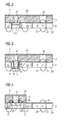
Figure 1A shows an embodiment of the optical sensor arrangement. The optical sensor arrangement comprises a three-dimensional integrated circuit with afirst layer 1, asecond layer 2, and amold layer 3, optionally covered by acover layer 4. - The
first layer 1 comprises a light-emitting device LED which, preferably, is a light-emitting diode. The light-emitting diode emits visible light but in the field of optical proximity sensors emission of (near) infrared light is preferred. IR diodes are both cheap and emit light that is not visible to the human eye. The latter is a beneficial aspect from a design point of view as optical proximity sensors typically reside behind a dark cover. If said cover is optically opaque to visible light but transparent to IR, the structure and circuitry are invisible to users and, thus, do not interfere with smartphone design, for instance. - The
second layer 2 comprises a silicon substrate and has amain surface 23 and a furthermain surface 24 opposite to themain surface 23. Thesecond layer 2 comprises a light-detector PD and a driver circuit IC. In this embodiment the light-detector PD and the driver circuit IC are integrated into thesecond layer 2. Alternatively, both components, LED, IC could be integrated into separate integrated circuits and connected to each other. The term "second layer" is used to cover both ways of integration. - The light-detector PD comprises a photo-diode which is sensitive to light to be emitted from the light-emitting device LED. Thus, in the preferred embodiment the photo-diode is sensitive to (near) infrared light. Alternatively, the light-detector PD may be a charge coupled device (CCD) or a CMOS light sensor. Typically, the latter devices are or can be manufactured to be sensitive to infrared. The driver circuit IC comprises means to control and operate both the light-detector PD and the light-emitting device LED. In this respect, the
second layer 2 comprises electrical connections between the driver circuit IC and both light-detector PD and the light-emitting device LED. - The
first layer 1 provides connection pads to thesecond layer 2 to allow the light emitting device LED to be operated. The connection to thesecond layer 2 is established through a metallization structuredtopology 11 which will be discussed in more detail with respect toFigures 7 to 9 . Briefly, thefirst layer 1, comprising the light emitting device LED, is bonded onto thesecond layer 2. The electrical connection is realized via the metallization structuredtopology 11 which connects the light-emitting device LED to the through-silicon via (TSV)connections 21. The metallization structuredtopology 11 is produced by means of high topology lithography, like EVG Nano spray lithography, and further by spray-coating or sputtering of a metal layer. - The
second layer 2 constitutes an active interposer. Apart from the through-silicon via (TSV)connections 21, the furthermain surface 24 comprises a redistribution layer or, alternatively, or may be connected to an embedded wafer level ball grid array, in order to make input/output pads available at locations of the optical sensor arrangement. This concerns electrical connections within the optical sensor arrangement, e.g. between the light-emitting device LED, the driver circuit IC and the light detector PD, as well as connections to further external circuits in a system into which the optical sensor arrangement is embedded, for example, a smartphone, mobile phone or mobile computer. Connections to such other circuits are established viabumps 25, located at the furthermain surface 24. - The
mold layer 3 covers a stack of first andsecond layer mold layer 3 has a characteristic shape which basically defines the optical paths within the optical sensor arrangement. The specifics of the mold shape is determined by the field of application of the optical sensor arrangement, e.g. optical proximity detection. The stack of first andsecond layer mold layer 3 make up a three-dimensional integrated circuit. - The
mold layer 3 constitutes a wafer level mold structure which is produced at a wafer level by using molding techniques like transfer molding such as film-assisted molding. This way typically more than one optical sensor arrangement is produced at a time and individual ones are cut out by sawing. The shape of a mold determines the structure of themold layer 3. In film-assisted molding, for example, a plastic film which is attached to an inner surface of the mold by vacuum before the first andsecond layer mold layer 3 to be produced. Finally, the cavity is filled with liquid mold material and, after the mold material has cured, themold layer 3 has taken the shape forced by the mold. - The mold is structured so that it shapes the
mold layer 3 to allow light emitted from the light-emitting device LED to leave the arrangement. At the same time it allows light to enter the arrangement and be detected by the light-detector PD. This functionality is implemented by means of a first andsecond aperture mold layer 3, respectively. In fact, the light-emitting device LED and the light-detector PD are placed in front of the first andsecond aperture first light barrier 33 is designed into themold layer 3 which resides between light-emitting device LED and the light-detector PD to block light from being transmitted directly between these two components. In this embodiment thefirst light barrier 33 is framed by the first andsecond apertures mold layer 3 comprises an optically opaque material so that no light can pass thefirst light barrier 33. One preferred material is plastics. - In addition to the
first light barrier 33, thesecond layer 2 comprises one or more secondlight barriers 22. Conveniently, this secondlight barrier 22 comprises through silicon vias in the shape of rectangles or rings around the light-emitting device LED and/or the light detector PD. This way, light emitted from the light-emitting device LED is blocked from reaching the light detector PD by way through the material of thesecond layer 2. Thesecond layer 2 is typically made of silicon substrate which to some degree is transparent to light, in particular infrared light. The secondlight barrier 22 thus further reduces optical crosstalk. - Optionally, the optical sensor arrangement can be covered by the
cover layer 4. Thecover layer 4 comprises a transparent or at least translucent mold material and seals the optical sensor arrangement of its surroundings. In particular, mold material can also fill the first and/orsecond aperture optical elements 41, which may have the shape of an optical lens and/or a zone plate like a Fresnel lens. Examples are discussed with respect to further embodiments and can be used with the present embodiment ofFigure 1A as well. - For example, the embodiment shown in
Figure 1B is the same as ofFigure 1A except that optical elements 41 (e.g. lenses) are connected to the light-emitting device LED and the light detector PD, respectively. In this embodiment the lenses reside inside the first andsecond aperture optical elements 41 shaping beams of light emitted by the light-emitting device LED and/or detected by the light detector PD to improve signal-to-noise ratio and reduce optical cross-talk. - The embodiment shown in
Figure 1C is based on that ofFigure 1C . Here, thelenses 41 reside on top of the first andsecond aperture -
Figure 2 shows another embodiment of the optical sensor arrangement. This embodiment is based on the ones disclosed inFigures 1A to 1C and only differs in the connection of thefirst layer 1 to thesecond layer 2. Thefirst layer 1 resides in a cavity which is etched into thesecond layer 2 in order to have the same surface height as thefirst layer 1. The light-emitting device LED is bonded into the cavity and electrically connected by means of a low topology lithography for metal contact as discussed above. The optical elements can be provided in the way discussed with respect toFigures 1A to 1C . -
Figure 3 shows another embodiment of the optical sensor arrangement. This embodiment is based on the ones disclosed inFigures 1A to 1C but differs in the way thefirst layer 1 is connected to thesecond layer 2. Thefirst aperture 31 is cut through thesecond layer 2 and themold layer 3 completely leaving ahole 34. Theadditional hole 34 in thesecond layer 2 is e.g. formed by a wide diameter TSV and a diffractive RIE etch before or after wafer level molding selective to the mold compound. - The
first layer 1 is connected to thesecond layer 2 in front of thehole 34 in a flip-chip fashion prior or after bumping. For this process thefirst layer 1 has solder pads and is then electrically connected to the second layer by (micro) bumps 27 on the furthermain surface 24 which provides metal contact via low topology lithography. Optionally, the optical sensor arrangement is provided withoptical elements 41 like lenses or zone plates as discussed above with respect toFigures 1A to 1C . -
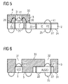
Figure 4 shows another embodiment of the optical sensor arrangement. This embodiment is based on the one disclosed inFigure 2 . Thefirst layer 1 resides in a cavity which is etched into thesecond layer 2. Different toFigure 2 the cavity for thefirst layer 1 is enlarged in order to have mold determiningside walls 35 with respect to thefirst layer 1. The light-emitting device LED is wire bonded 26 to electrically connect to thesecond layer 2. - Furthermore, the
mold layer 3 covers only part of themain surface 23 and there is nosecond aperture 32. Optionally, the optical sensor arrangement is provided with optical elements like lenses or zone plates as discussed above with respect toFigures 1A to 1C . Consequently, theoptional cover 4 also only covers part of themold layer 3. -
Figure 5 shows another embodiment of the optical sensor arrangement based on the one disclosed inFigure 4 . There is no cavity, however, and the first layer is directly connected on top of thesecond layer 2. The electrical connection is established via wire bonds 26. Similar toFigure 4 themold layer 3 is only around thefirst layer 1 asfirst light barrier 33 but not over the remaining surface of thesecond layer 2 in order to minimize wafer bow due to the stress of the molding. -
Figure 6 shows another embodiment of the optical sensor arrangement. This embodiment is somewhat different from the ones presented with respect toFigures 1A to 5 . In the integration of the latter embodiments the first andsecond layer first layer 1 and thesecond layer 2 are overmolded by themold layer 3. - The three-dimensional integrated circuit is thus established in a horizontal arrangement of first and
second layer mold layer 3. Electrical connection are provided via a redistribution layer or an embedded wafer level ball grid array along anothermain surface 5 on the bottom side of the optical sensor arrangement. Bump connections are provided on this anothermain surface 5. - The first and
second aperture cover 4, are provided according to the design principles discussed above. Also optical elements can be attached to both thefirst layer 1 and thesecond layer 2 as discussed above. - Typical dimensions of the embodiments of the optical sensor arrangement may be as follows. The light emitting diode preferably is a GaN light emitting diode having a thickness of several 10 µm to 180 µm. The lower thickness can be realized e.g. for new GaN on Si LEDs. The LED footprint is typically smaller than 350 µm times 350 µm. Larger bumps have about 100 to 300 µm whereas microbumps for LED mounting are smaller than 50 µm. The wafer level molded
layer 3 and its flight barrier have 100 to 1000 µm height. - The operation of the different embodiments of the optical sensor arrangement for proximity detection is similar. The light-emitting device LED emits light, either continuously or in a pulsed fashion. Due to the
first light barrier 33 in themold layer 3 the light-detector PD detects light emitted from the light-emitting device LED only if it gets reflected by a proximity object, i.e. the first light barrier blocks light from being transmitted directly from the light-emitting device to the light-detector. However, the light-detector PD is typically also exposed to ambient light from the surroundings of the optical sensor arrangement. To account for this contribution the control device IC comprises means to record the amount of ambient light and correct for it. For example, this can be achieved by letting the light-emitting device LED emit pulses of a certain duration. During the pauses when no light is emitted the light-detector LED only detects ambient light. The control device IC typically comprises further means for signal processing not shown and discussed here. -
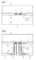
Figure 7 is a cross section of thesecond layer 2 which constitutes an active interposer with adielectric layer 7 and embedded metal layers on itsmain surface 23. An integrated circuit, for example, control device IC, or light-detector PD can be connected to the metallization structuredtopology 11 comprising several metal layers, which serve as a wiring. Manufacture is facilitated if ahandling wafer 6 is fastened to an upper surface of thedielectric layer 7. A through-silicon via (TSV) connection is produced from the furthermain surface 24 of thesecond layer 2, opposite thedielectric layer 7. -
Figure 8 is a cross section according toFigure 7 after the formation of the through-silicon via (TSV) connection. Afurther dielectric layer 8 is arranged above the furthermain surface 24. The through-silicon via (TSV) connection can be produced by etching a via hole through thefurther dielectric layer 8 and thesecond layer 2, until acontact area 9 of one of the metal layers 11 is uncovered. Asidewall insulation 13 is preferably formed in the via hole, and a metallization is applied in the via hole, so that the metallization electrically contacts thecontact area 9. The metallization yields the electrically conductive interconnection of the through-silicon via (TSV)connection 21. At least onefurther metal layer 14, for example, a redistribution layer, which is connected to the through-silicon via (TSV)connection 21, is arranged in or on thefurther dielectric layer 8. The inner volume of the through-silicon via (TSV)connection 21 can be filled with the material that is applied to form thefurther dielectric layer 8, which may be an oxide or nitride of semiconductor material, for instance. Afurther contact area 19 of thefurther metal layer 14 can be provided for an external electrical connection. The handlingwafer 6 is then removed. -
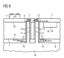
Figure 9 is a cross section according toFigure 7 after the placement of chips like the light-detector PD or driver circuit IC. Manufacture is facilitated if afurther handling wafer 16 is fastened to thefurther dielectric layer 8. A chip like thefirst layer 1 comprising the light-emitting device LED is mounted on thedielectric layer 7. Any number of chips can thus be mounted above themain surface 23. -
- 1
- first layer
- 11
- metallization structured topology
- 13
- sidewall insulation
- 14
- further metal layer
- 16
- further handling wafer
- 19
- further contact area
- 2
- second layer
- 21
- through-silicon via (TSV) connection
- 22
- second light barrier
- 23
- main surface
- 24
- further main surface
- 25
- bump
- 26
- bond wire
- 27
- micro bump
- 3
- mold layer
- 31
- first aperture
- 32
- second aperture
- 33
- first light barrier
- 35
- side wall
- 4
- cover layer
- 41
- optical element
- 5
- another main surface
- 6
- handling wafer
- 7
- dielectric layer
- 8
- further dielectric layer
- 9
- contact area
- IC
- driver circuit
- LED
- light-emitting device
- PD
- light detector
Claims (16)
- Optical sensor arrangement, in particular an optical proximity sensor arrangement, comprising a three-dimensional integrated circuit further comprising:- a first layer (1) comprising a light-emitting device (LED),- a second layer (2) comprising a light-detector (PD) and a driver circuit (IC) electrically connected to the light-emitting device (LED) and to the light-detector (PD) and configured to control the operation of the light-emitting device (LED) and the light-detector (PD), and- a mold layer (3) comprising a first light-barrier (33) between the light-emitting device (LED) and the light-detector (PD) configured to block light from being transmitted directly from the light-emitting device (LED) to the light-detector (PD).
- Optical sensor arrangement according to claim 1, wherein the mold layer (3) comprises an optically opaque mold material.
- Optical sensor arrangement according to claim 1 or 2, wherein the mold layer (3) comprises a wafer-level mold structure.
- Optical sensor arrangement according to one of claims 1 to 3, wherein the mold layer is at least partially connected to a main surface (23) of the second layer (2) and comprises a first aperture (31) to which the first layer (1) is attached such that light from the light-emitting device (LED) can be emitted through the first aperture (31).
- Optical sensor arrangement according to claims 4, wherein the mold layer (3) comprises a second aperture (32) to which the light-detector (PD) is attached such that light can reach the light-detector (PD) to be detected.
- Optical sensor arrangement according to one of claims 1 to 5, wherein the second layer (2) comprises a substrate into which the light-detector (PD) and the driver circuit (IC) are integrated.
- Optical sensor arrangement according to claims 6, wherein the substrate comprises an active interposer, in particular connected to a redistribution layer or an embedded wafer level ball grid array.
- Optical sensor arrangement according to one of claims 1 to 7, wherein the light-emitting device (LED) is electrically connected to the second layer (2) by means of a metallization structured topology (11), a bond wire (26) or a redistribution layer.
- Optical sensor arrangement according to one of claims 1 to 8, wherein- the first layer (1) is stacked onto the main surface (23) of the second layer (2) or- the first layer (1) is embedded into a recess formed in the second layer (2) or- the first layer (1) is stacked onto a further main surface (24) of the second layer (2) opposite to the main surface (23) and wherein the first aperture (31) extends through the second layer (2).
- Optical sensor arrangement according to one of claims 1 to 7, wherein the second layer (2) comprises a second light barrier (22).
- Optical sensor arrangement according to claim 10, wherein the second light barrier (22) comprises through silicon vias designed into the substrate.
- Optical sensor arrangement according to one of claims 4 to 9, wherein the light-detector (PD) and/or light-emitting device (LED) are covered by an optical element (41) and wherein the optical element (41) is a lens and/or zone plate, in particular a nano-imprinted lens.
- Method of producing an optical sensor arrangement, in particular of producing an optical proximity sensor arrangement, comprising the steps of:- integrating a light-emitting device (LED) into a first layer (1),- integrating a light-detector (PD) and a driver circuit (IC) into a second layer (2),- electrically connecting the light-emitting device (LED) to the driver circuit (IC) and to the light-detector (PD),- molding a mold layer (3) comprising a first light-barrier (33) between the light-emitting device (LED) and the light-detector (PD) configured to block light from being transmitted directly from the light-emitting device (LED) to the light-detector (PD) and- integrating the first layer (1), the second layer (2) and the mold layer (3) into a three dimensional integrated circuit.
- Method according to claim 13, wherein the molding involves molding at a waver-level, in particular using an optically opaque material.
- Method according to claim 13 or 14, wherein- the first layer (1) is stacked onto the second layer (2), in particular stacked by means of die-to-wafer stacking and the first layer (1) is electrically connected to the second layer (2) by means of a metallization structured topology (11), a bond wire (26) or a redistribution layer, in particular by means of a metallization structured topology with through-silicon-vias, or- the first layer is embedded into a recess formed in the second layer (2).
- Method according to one of claims 13 to 15, further comprising the steps of- connecting the mold layer (3) at least partially to a main surface (23) of the second layer (2) and providing a first aperture (31) in the mold layer (3) to which the first layer (1) is attached such that light from the light-emitting device (LED) can be emitted through the first aperture (31) and/or- provide a second aperture (32) to which the light-detector (PD) is attached such that light can reach the light-detector (PD) to be detected.
Priority Applications (4)
| Application Number | Priority Date | Filing Date | Title |
|---|---|---|---|
| US15/101,893 US9684074B2 (en) | 2013-12-05 | 2014-12-03 | Optical sensor arrangement and method of producing an optical sensor arrangement |
| PCT/EP2014/076420 WO2015082549A1 (en) | 2013-12-05 | 2014-12-03 | Optical sensor arrangement and method of producing an optical sensor arrangement |
| CN201480065588.7A CN105793727B (en) | 2013-12-05 | 2014-12-03 | Optical sensor arrangement and the method for manufacturing optical sensor arrangement |
| JP2016536703A JP6466943B2 (en) | 2013-12-05 | 2014-12-03 | Optical sensor assembly and method of manufacturing optical sensor assembly |
Applications Claiming Priority (1)
| Application Number | Priority Date | Filing Date | Title |
|---|---|---|---|
| US201361912099P | 2013-12-05 | 2013-12-05 |
Publications (2)
| Publication Number | Publication Date |
|---|---|
| EP2881753A1 true EP2881753A1 (en) | 2015-06-10 |
| EP2881753B1 EP2881753B1 (en) | 2019-03-06 |
Family
ID=49920048
Family Applications (1)
| Application Number | Title | Priority Date | Filing Date |
|---|---|---|---|
| EP13199086.3A Active EP2881753B1 (en) | 2013-12-05 | 2013-12-20 | Optical sensor arrangement and method of producing an optical sensor arrangement |
Country Status (5)
| Country | Link |
|---|---|
| US (1) | US9684074B2 (en) |
| EP (1) | EP2881753B1 (en) |
| JP (1) | JP6466943B2 (en) |
| CN (1) | CN105793727B (en) |
| WO (1) | WO2015082549A1 (en) |
Cited By (3)
| Publication number | Priority date | Publication date | Assignee | Title |
|---|---|---|---|---|
| EP3340296B1 (en) * | 2016-12-20 | 2019-10-02 | Melexis Technologies NV | Light emitting diode device |
| CN113167863A (en) * | 2018-09-04 | 2021-07-23 | ams有限公司 | Optical sensor device, apparatus and method of manufacturing optical sensor device |
| EP4179580A4 (en) * | 2020-08-14 | 2024-07-24 | Avicenatech Corp. | Microled based time of flight system |
Families Citing this family (63)
| Publication number | Priority date | Publication date | Assignee | Title |
|---|---|---|---|---|
| JP6221582B2 (en) * | 2013-09-30 | 2017-11-01 | セイコーエプソン株式会社 | Ultrasonic device and probe, electronic apparatus and ultrasonic imaging apparatus |
| US9305967B1 (en) * | 2015-04-16 | 2016-04-05 | Intersil Americas LLC | Wafer Level optoelectronic device packages and methods for making the same |
| EP3121853B1 (en) | 2015-07-23 | 2022-01-19 | ams AG | Method of producing an optical sensor at wafer-level and optical sensor |
| US10061057B2 (en) | 2015-08-21 | 2018-08-28 | Stmicroelectronics (Research & Development) Limited | Molded range and proximity sensor with optical resin lens |
| US11069667B2 (en) * | 2016-03-31 | 2021-07-20 | Stmicroelectronics Pte Ltd | Wafer level proximity sensor |
| US11226402B2 (en) * | 2016-06-09 | 2022-01-18 | Ams Sensors Singapore Pte. Ltd. | Optical ranging systems including optical cross-talk reducing features |
| US9911890B2 (en) * | 2016-06-30 | 2018-03-06 | Stmicroelectronics Pte Ltd | Optical sensor package including a cavity formed in an image sensor die |
| WO2018089795A1 (en) | 2016-11-10 | 2018-05-17 | Qoravita LLC | System and method for applying a low frequency magnetic field to biological tissues |
| US10276764B2 (en) * | 2016-12-21 | 2019-04-30 | Glo Ab | Micro-lensed light emitting device |
| DE102017110216B4 (en) * | 2017-05-11 | 2023-03-09 | OSRAM Opto Semiconductors Gesellschaft mit beschränkter Haftung | Optoelectronic sensor module and method for producing an optoelectronic sensor module |
| CN107329589B (en) * | 2017-06-29 | 2020-03-27 | 努比亚技术有限公司 | Control device of function key |
| US10267988B2 (en) | 2017-06-30 | 2019-04-23 | Taiwan Semiconductor Manufacturing Company, Ltd. | Photonic package and method forming same |
| DE102017124815B4 (en) * | 2017-06-30 | 2019-10-17 | Taiwan Semiconductor Manufacturing Company, Ltd. | Photonic package and method for its formation |
| US10461744B2 (en) | 2017-09-21 | 2019-10-29 | Google Llc | Proximity sensor connection mechanism |
| EP3470872B1 (en) * | 2017-10-11 | 2021-09-08 | Melexis Technologies NV | Sensor device |
| DE102017124319A1 (en) | 2017-10-18 | 2019-04-18 | Osram Opto Semiconductors Gmbh | Semiconductor device |
| CN108226955B (en) * | 2017-12-26 | 2020-04-14 | 杭州艾米机器人有限公司 | Infrared Array Proximity Sensor |
| TWI672786B (en) * | 2017-12-28 | 2019-09-21 | Phoenix & Corporation | Electronic package and method of manufacture |
| DE102018100946A1 (en) * | 2018-01-17 | 2019-07-18 | Osram Opto Semiconductors Gmbh | COMPONENT AND METHOD FOR PRODUCING A COMPONENT |
| US11038077B2 (en) * | 2018-03-05 | 2021-06-15 | Xintec Inc. | Chip package and manufacturing method thereof |
| FR3081256B1 (en) | 2018-05-18 | 2020-07-31 | St Microelectronics Grenoble 2 | OPTICAL TRANSMISSION / RECEPTION CIRCUIT |
| FR3081257B1 (en) * | 2018-05-18 | 2020-07-31 | St Microelectronics Grenoble 2 | OPTICAL TRANSMISSION / RECEPTION CIRCUIT |
| US11143551B2 (en) * | 2018-05-18 | 2021-10-12 | Hana Microelectronics, Inc. | Proximity sensor with infrared ink coating |
| US11520074B2 (en) | 2018-09-14 | 2022-12-06 | Hana Microelectronics, Inc. | Proximity sensor with light blocking barrier comprising a gap having a cross-section with parallel walls between emitter and detector |
| US11244937B2 (en) * | 2018-10-09 | 2022-02-08 | Industrial Technology Research Institute | Spliced display with LED modules disposed on transparent substrate |
| TWI680593B (en) * | 2018-10-12 | 2019-12-21 | 欣興電子股份有限公司 | Light emitting device package structure and manufacturing method thereof |
| JP7368081B2 (en) * | 2018-10-23 | 2023-10-24 | 旭化成エレクトロニクス株式会社 | optical device |
| DE102018218166A1 (en) * | 2018-10-24 | 2020-04-30 | Osram Gmbh | DISTANCE MEASURING UNIT |
| DE102018127627B4 (en) * | 2018-11-06 | 2020-08-20 | Sick Ag | Photoelectric sensor device |
| US11567198B2 (en) | 2019-03-25 | 2023-01-31 | Hana Microelectronics Inc. | Proximity sensor with light inhibiting barrier comprising a gap having a cross-section with parallel walls substantially perpendicular to the top surface of an optically transmissive material |
| US11662435B2 (en) * | 2019-04-04 | 2023-05-30 | Liturex (Guangzhou) Co. Ltd | Chip scale integrated scanning LiDAR sensor |
| JP7245721B2 (en) | 2019-05-31 | 2023-03-24 | 株式会社アドバンテスト | Test equipment, test methods and programs |
| US11549799B2 (en) | 2019-07-01 | 2023-01-10 | Apple Inc. | Self-mixing interference device for sensing applications |
| US11383970B2 (en) * | 2019-07-09 | 2022-07-12 | Amkor Technology Singapore Holding Pte. Ltd. | Semiconductor devices and related methods |
| US11769843B1 (en) * | 2019-07-30 | 2023-09-26 | Hrl Laboratories, Llc | Photonic integrated module with metal embedded chips |
| KR102801218B1 (en) * | 2019-08-30 | 2025-04-29 | 삼성전자주식회사 | Display module package |
| US11262966B2 (en) | 2019-09-27 | 2022-03-01 | Apple Inc. | Electromagnetic band gap structures |
| US11862749B2 (en) * | 2019-12-06 | 2024-01-02 | Adesto Technologies Corporation | Integrated module assembly for optical integrated circuits |
| US11594663B2 (en) | 2019-12-20 | 2023-02-28 | Nanosys, Inc. | Light emitting diode device containing a micro lens array and method of making the same |
| US11828944B1 (en) * | 2020-04-09 | 2023-11-28 | Apple Inc. | Head-mounted device with optical module illumination systems |
| US12002898B2 (en) * | 2020-06-22 | 2024-06-04 | Stmicroelectronics Pte Ltd | Embedded wafer level optical sensor packaging |
| KR102498875B1 (en) * | 2020-09-29 | 2023-02-13 | 주식회사 라이팩 | Fabrication method of optic device package and optic device |
| EP4222784A4 (en) * | 2020-10-08 | 2024-06-26 | Avicenatech Corp. | Integration of oe devices with ics |
| GB202019666D0 (en) * | 2020-12-14 | 2021-01-27 | Ams Sensors Singapore Pte Ltd | Wafer-level manufacture of optical packages |
| JP7374937B2 (en) | 2021-01-13 | 2023-11-07 | 株式会社アドバンテスト | Test equipment, test methods and programs |
| JP7386190B2 (en) | 2021-01-21 | 2023-11-24 | 株式会社アドバンテスト | Test equipment, test methods and programs |
| DE102021104189A1 (en) | 2021-02-22 | 2022-08-25 | OSRAM Opto Semiconductors Gesellschaft mit beschränkter Haftung | SENSING DEVICE |
| JP7355773B2 (en) | 2021-02-26 | 2023-10-03 | 株式会社アドバンテスト | Test equipment, test methods and programs |
| US20250004107A1 (en) * | 2021-07-23 | 2025-01-02 | Ams-Osram Asia Pacific Pte. Ltd. | Sensor package and method of manufacturing a sensor package |
| JP7355789B2 (en) | 2021-09-08 | 2023-10-03 | 株式会社アドバンテスト | Test equipment, test methods and programs |
| US12413043B2 (en) | 2021-09-21 | 2025-09-09 | Apple Inc. | Self-mixing interference device with tunable microelectromechanical system |
| JP2023085909A (en) * | 2021-12-09 | 2023-06-21 | ローム株式会社 | light sensor |
| CN120496135A (en) * | 2022-01-17 | 2025-08-15 | 群创光电股份有限公司 | Electronic device |
| JP2025513701A (en) * | 2022-03-21 | 2025-04-30 | ソニーセミコンダクタソリューションズ株式会社 | Time-of-flight systems and methods |
| JPWO2024029086A1 (en) * | 2022-08-05 | 2024-02-08 | ||
| US20240061084A1 (en) * | 2022-08-22 | 2024-02-22 | Oip Technology Pte Ltd | Driver chip, packaging method for optical filter structure, optical sensor device and packaging method thereof |
| US12613131B2 (en) * | 2022-09-22 | 2026-04-28 | Apple Inc. | Optical proximity sensor |
| DE102022124732A1 (en) * | 2022-09-26 | 2024-03-28 | Ams-Osram International Gmbh | METHOD FOR PRODUCING AN OPTOELECTRONIC COMPONENT AND OPTOELECTRONIC COMPONENT |
| CN115685146A (en) * | 2022-11-15 | 2023-02-03 | 业泓科技(成都)有限公司 | Direct Time-of-Flight Sensing Module |
| CN116093095B (en) * | 2022-12-14 | 2024-06-14 | 莱弗利科技(苏州)有限公司 | Optocoupler isolator and packaging process thereof |
| JP7556080B2 (en) * | 2023-03-03 | 2024-09-25 | セイコーNpc株式会社 | Optical device and method for manufacturing optical device |
| US12601583B2 (en) | 2023-05-17 | 2026-04-14 | Apple Inc. | Multi-channel self-mixing interferometric sensor |
| WO2025012223A1 (en) * | 2023-07-10 | 2025-01-16 | Sensibel As | Optical readout module |
Citations (5)
| Publication number | Priority date | Publication date | Assignee | Title |
|---|---|---|---|---|
| DE3633181A1 (en) * | 1986-09-30 | 1988-04-07 | Siemens Ag | METHOD FOR PRODUCING AN OPTO COUPLER OR A REFLECTIVE LIGHT BARRIER AND RELATED OPTOCOUPLER OR RELATED REFLECTIVE BARRIER |
| US6486467B1 (en) * | 1998-12-23 | 2002-11-26 | Dr. Johannes Heiden Hain Gmbh | Optical detector for measuring relative displacement of an object on which a grated scale is formed |
| US7030359B2 (en) * | 2002-03-07 | 2006-04-18 | CiS Institut für Mikrosensorik gGmbH | Sensor detecting reflected light and method for its manufacture |
| US8212202B2 (en) * | 2009-01-08 | 2012-07-03 | Avago Technologies Ecbu Ip (Singapore) Pte. Ltd. | Reflective optical encoder package and method |
| US20130009173A1 (en) * | 2011-07-08 | 2013-01-10 | Stmicroelectronics (Grenoble 2) Sas | Optical electronic package |
Family Cites Families (28)
| Publication number | Priority date | Publication date | Assignee | Title |
|---|---|---|---|---|
| JP2985691B2 (en) * | 1994-03-23 | 1999-12-06 | 株式会社デンソー | Semiconductor device |
| JP2001024150A (en) | 1999-07-06 | 2001-01-26 | Sony Corp | Semiconductor device |
| JP4711029B2 (en) * | 2000-12-04 | 2011-06-29 | 住友電気工業株式会社 | Optical communication device |
| DE10352741B4 (en) | 2003-11-12 | 2012-08-16 | Austriamicrosystems Ag | Radiation-detecting optoelectronic component, process for its production and use |
| JP4252019B2 (en) | 2004-09-01 | 2009-04-08 | 三洋電機株式会社 | Circuit device and manufacturing method thereof |
| JP4061409B2 (en) * | 2004-11-09 | 2008-03-19 | 国立大学法人九州大学 | Sensor unit and biosensor |
| JP2006203111A (en) * | 2005-01-24 | 2006-08-03 | Hosiden Corp | Object detection sensor |
| KR100721353B1 (en) | 2005-07-08 | 2007-05-25 | 삼성전자주식회사 | Structure and Manufacturing Method of Chip Insert Intermediate Substrate, Wafer Level Stacking Structure and Package Structure of Heterogeneous Chip |
| JP2007027621A (en) * | 2005-07-21 | 2007-02-01 | Rohm Co Ltd | Surface mount type photo interrupter and manufacturing method thereof |
| JP2007199328A (en) * | 2006-01-26 | 2007-08-09 | Fuji Xerox Co Ltd | Optical coupling device |
| JP2010034189A (en) * | 2008-07-28 | 2010-02-12 | Sharp Corp | Optical proximity sensor, method of manufacturing the same, and electronic apparatus mounted with the same |
| JP4871344B2 (en) * | 2008-11-25 | 2012-02-08 | 株式会社東芝 | Light emitting device and manufacturing method thereof |
| US7838337B2 (en) | 2008-12-01 | 2010-11-23 | Stats Chippac, Ltd. | Semiconductor device and method of forming an interposer package with through silicon vias |
| US8097964B2 (en) | 2008-12-29 | 2012-01-17 | Texas Instruments Incorporated | IC having TSV arrays with reduced TSV induced stress |
| US8324602B2 (en) | 2009-04-14 | 2012-12-04 | Intersil Americas Inc. | Optical sensors that reduce specular reflections |
| US8779361B2 (en) * | 2009-06-30 | 2014-07-15 | Avago Technologies General Ip (Singapore) Pte. Ltd. | Optical proximity sensor package with molded infrared light rejection barrier and infrared pass components |
| US8587129B2 (en) | 2009-07-31 | 2013-11-19 | Stats Chippac Ltd. | Integrated circuit packaging system with through silicon via base and method of manufacture thereof |
| US20110089531A1 (en) | 2009-10-16 | 2011-04-21 | Teledyne Scientific & Imaging, Llc | Interposer Based Monolithic Microwave Integrate Circuit (iMMIC) |
| US20110186960A1 (en) | 2010-02-03 | 2011-08-04 | Albert Wu | Techniques and configurations for recessed semiconductor substrates |
| US8492720B2 (en) * | 2010-06-08 | 2013-07-23 | Avago Technologies General Ip (Singapore) Pte. Ltd. | Small low-profile optical proximity sensor |
| US8518746B2 (en) | 2010-09-02 | 2013-08-27 | Stats Chippac, Ltd. | Semiconductor device and method of forming TSV semiconductor wafer with embedded semiconductor die |
| US8928159B2 (en) | 2010-09-02 | 2015-01-06 | Taiwan Semiconductor Manufacturing & Company, Ltd. | Alignment marks in substrate having through-substrate via (TSV) |
| TWI434387B (en) | 2010-10-11 | 2014-04-11 | 日月光半導體製造股份有限公司 | Semiconductor device having via hole and package structure of semiconductor device having via hole and manufacturing method thereof |
| US9398694B2 (en) | 2011-01-18 | 2016-07-19 | Sony Corporation | Method of manufacturing a package for embedding one or more electronic components |
| FR2973573A1 (en) * | 2011-04-01 | 2012-10-05 | St Microelectronics Grenoble 2 | SEMICONDUCTOR HOUSING COMPRISING AN OPTICAL SEMICONDUCTOR DEVICE |
| JP5399525B2 (en) * | 2011-06-29 | 2014-01-29 | シャープ株式会社 | Optical distance measuring device and electronic device |
| US9385058B1 (en) | 2012-12-29 | 2016-07-05 | Monolithic 3D Inc. | Semiconductor device and structure |
| US9525094B2 (en) * | 2015-03-27 | 2016-12-20 | Stmicroelectronics (Grenoble 2) Sas | Proximity and ranging sensor |
-
2013
- 2013-12-20 EP EP13199086.3A patent/EP2881753B1/en active Active
-
2014
- 2014-12-03 WO PCT/EP2014/076420 patent/WO2015082549A1/en not_active Ceased
- 2014-12-03 JP JP2016536703A patent/JP6466943B2/en active Active
- 2014-12-03 CN CN201480065588.7A patent/CN105793727B/en active Active
- 2014-12-03 US US15/101,893 patent/US9684074B2/en active Active
Patent Citations (5)
| Publication number | Priority date | Publication date | Assignee | Title |
|---|---|---|---|---|
| DE3633181A1 (en) * | 1986-09-30 | 1988-04-07 | Siemens Ag | METHOD FOR PRODUCING AN OPTO COUPLER OR A REFLECTIVE LIGHT BARRIER AND RELATED OPTOCOUPLER OR RELATED REFLECTIVE BARRIER |
| US6486467B1 (en) * | 1998-12-23 | 2002-11-26 | Dr. Johannes Heiden Hain Gmbh | Optical detector for measuring relative displacement of an object on which a grated scale is formed |
| US7030359B2 (en) * | 2002-03-07 | 2006-04-18 | CiS Institut für Mikrosensorik gGmbH | Sensor detecting reflected light and method for its manufacture |
| US8212202B2 (en) * | 2009-01-08 | 2012-07-03 | Avago Technologies Ecbu Ip (Singapore) Pte. Ltd. | Reflective optical encoder package and method |
| US20130009173A1 (en) * | 2011-07-08 | 2013-01-10 | Stmicroelectronics (Grenoble 2) Sas | Optical electronic package |
Cited By (5)
| Publication number | Priority date | Publication date | Assignee | Title |
|---|---|---|---|---|
| EP3340296B1 (en) * | 2016-12-20 | 2019-10-02 | Melexis Technologies NV | Light emitting diode device |
| CN113167863A (en) * | 2018-09-04 | 2021-07-23 | ams有限公司 | Optical sensor device, apparatus and method of manufacturing optical sensor device |
| CN113167863B (en) * | 2018-09-04 | 2024-03-19 | ams有限公司 | Optical sensor device, equipment and method of manufacturing optical sensor device |
| US12140699B2 (en) | 2018-09-04 | 2024-11-12 | Ams Ag | Optical sensor arrangement, device and method of manufacturing an optical sensor arrangement |
| EP4179580A4 (en) * | 2020-08-14 | 2024-07-24 | Avicenatech Corp. | Microled based time of flight system |
Also Published As
| Publication number | Publication date |
|---|---|
| CN105793727B (en) | 2018-01-16 |
| US9684074B2 (en) | 2017-06-20 |
| WO2015082549A1 (en) | 2015-06-11 |
| EP2881753B1 (en) | 2019-03-06 |
| JP6466943B2 (en) | 2019-02-06 |
| CN105793727A (en) | 2016-07-20 |
| US20160306042A1 (en) | 2016-10-20 |
| JP2017504959A (en) | 2017-02-09 |
Similar Documents
| Publication | Publication Date | Title |
|---|---|---|
| US9684074B2 (en) | Optical sensor arrangement and method of producing an optical sensor arrangement | |
| US10749067B2 (en) | Optical sensor package including a cavity formed in an image sensor die | |
| CN110223975B (en) | Optical device, optical module structure and manufacturing process | |
| JP6789219B2 (en) | Image sensor device | |
| US9496247B2 (en) | Integrated camera module and method of making same | |
| CN205645806U (en) | Proximity sensor | |
| CN111052406B (en) | Methods of fabricating multiple time-of-flight sensor devices | |
| US9543282B2 (en) | Optical sensor package | |
| CN216285703U (en) | Stacked optical sensing package | |
| CN206876296U (en) | Optical sensor and electronic device | |
| EP4481817A1 (en) | Sensor and tof camera using same | |
| CN215955279U (en) | Optical sensing package | |
| CN109585434B (en) | Wafer-level light sensing system packaging structure and manufacturing method thereof | |
| CN100585850C (en) | Image sensing module with crystal grain three-dimensional stacking structure | |
| CN116569323A (en) | Optical device package manufacturing method and optical device package | |
| CN117836955A (en) | Sensor package and method of manufacturing the same |
Legal Events
| Date | Code | Title | Description |
|---|---|---|---|
| PUAI | Public reference made under article 153(3) epc to a published international application that has entered the european phase |
Free format text: ORIGINAL CODE: 0009012 |
|
| 17P | Request for examination filed |
Effective date: 20131220 |
|
| AK | Designated contracting states |
Kind code of ref document: A1 Designated state(s): AL AT BE BG CH CY CZ DE DK EE ES FI FR GB GR HR HU IE IS IT LI LT LU LV MC MK MT NL NO PL PT RO RS SE SI SK SM TR |
|
| AX | Request for extension of the european patent |
Extension state: BA ME |
|
| R17P | Request for examination filed (corrected) |
Effective date: 20151204 |
|
| RBV | Designated contracting states (corrected) |
Designated state(s): AL AT BE BG CH CY CZ DE DK EE ES FI FR GB GR HR HU IE IS IT LI LT LU LV MC MK MT NL NO PL PT RO RS SE SI SK SM TR |
|
| GRAP | Despatch of communication of intention to grant a patent |
Free format text: ORIGINAL CODE: EPIDOSNIGR1 |
|
| STAA | Information on the status of an ep patent application or granted ep patent |
Free format text: STATUS: GRANT OF PATENT IS INTENDED |
|
| RIC1 | Information provided on ipc code assigned before grant |
Ipc: H01L 31/0232 20140101ALI20181002BHEP Ipc: G01S 17/02 20060101ALI20181002BHEP Ipc: H01L 31/12 20060101ALI20181002BHEP Ipc: H01L 27/144 20060101ALI20181002BHEP Ipc: H01L 25/16 20060101ALI20181002BHEP Ipc: H01L 31/167 20060101ALI20181002BHEP Ipc: G01S 7/481 20060101AFI20181002BHEP |
|
| INTG | Intention to grant announced |
Effective date: 20181029 |
|
| RAP1 | Party data changed (applicant data changed or rights of an application transferred) |
Owner name: AMS AG |
|
| GRAS | Grant fee paid |
Free format text: ORIGINAL CODE: EPIDOSNIGR3 |
|
| GRAA | (expected) grant |
Free format text: ORIGINAL CODE: 0009210 |
|
| STAA | Information on the status of an ep patent application or granted ep patent |
Free format text: STATUS: THE PATENT HAS BEEN GRANTED |
|
| AK | Designated contracting states |
Kind code of ref document: B1 Designated state(s): AL AT BE BG CH CY CZ DE DK EE ES FI FR GB GR HR HU IE IS IT LI LT LU LV MC MK MT NL NO PL PT RO RS SE SI SK SM TR |
|
| REG | Reference to a national code |
Ref country code: GB Ref legal event code: FG4D |
|
| REG | Reference to a national code |
Ref country code: CH Ref legal event code: EP Ref country code: AT Ref legal event code: REF Ref document number: 1105289 Country of ref document: AT Kind code of ref document: T Effective date: 20190315 |
|
| REG | Reference to a national code |
Ref country code: DE Ref legal event code: R096 Ref document number: 602013051770 Country of ref document: DE |
|
| REG | Reference to a national code |
Ref country code: IE Ref legal event code: FG4D |
|
| REG | Reference to a national code |
Ref country code: DE Ref legal event code: R081 Ref document number: 602013051770 Country of ref document: DE Owner name: AMS AG, AT Free format text: FORMER OWNER: AMS AG, UNTERPREMSTAETTEN, AT |
|
| REG | Reference to a national code |
Ref country code: NL Ref legal event code: MP Effective date: 20190306 |
|
| REG | Reference to a national code |
Ref country code: LT Ref legal event code: MG4D |
|
| PG25 | Lapsed in a contracting state [announced via postgrant information from national office to epo] |
Ref country code: NO Free format text: LAPSE BECAUSE OF FAILURE TO SUBMIT A TRANSLATION OF THE DESCRIPTION OR TO PAY THE FEE WITHIN THE PRESCRIBED TIME-LIMIT Effective date: 20190606 Ref country code: LT Free format text: LAPSE BECAUSE OF FAILURE TO SUBMIT A TRANSLATION OF THE DESCRIPTION OR TO PAY THE FEE WITHIN THE PRESCRIBED TIME-LIMIT Effective date: 20190306 Ref country code: SE Free format text: LAPSE BECAUSE OF FAILURE TO SUBMIT A TRANSLATION OF THE DESCRIPTION OR TO PAY THE FEE WITHIN THE PRESCRIBED TIME-LIMIT Effective date: 20190306 Ref country code: FI Free format text: LAPSE BECAUSE OF FAILURE TO SUBMIT A TRANSLATION OF THE DESCRIPTION OR TO PAY THE FEE WITHIN THE PRESCRIBED TIME-LIMIT Effective date: 20190306 |
|
| PG25 | Lapsed in a contracting state [announced via postgrant information from national office to epo] |
Ref country code: NL Free format text: LAPSE BECAUSE OF FAILURE TO SUBMIT A TRANSLATION OF THE DESCRIPTION OR TO PAY THE FEE WITHIN THE PRESCRIBED TIME-LIMIT Effective date: 20190306 Ref country code: HR Free format text: LAPSE BECAUSE OF FAILURE TO SUBMIT A TRANSLATION OF THE DESCRIPTION OR TO PAY THE FEE WITHIN THE PRESCRIBED TIME-LIMIT Effective date: 20190306 Ref country code: LV Free format text: LAPSE BECAUSE OF FAILURE TO SUBMIT A TRANSLATION OF THE DESCRIPTION OR TO PAY THE FEE WITHIN THE PRESCRIBED TIME-LIMIT Effective date: 20190306 Ref country code: RS Free format text: LAPSE BECAUSE OF FAILURE TO SUBMIT A TRANSLATION OF THE DESCRIPTION OR TO PAY THE FEE WITHIN THE PRESCRIBED TIME-LIMIT Effective date: 20190306 Ref country code: BG Free format text: LAPSE BECAUSE OF FAILURE TO SUBMIT A TRANSLATION OF THE DESCRIPTION OR TO PAY THE FEE WITHIN THE PRESCRIBED TIME-LIMIT Effective date: 20190606 Ref country code: GR Free format text: LAPSE BECAUSE OF FAILURE TO SUBMIT A TRANSLATION OF THE DESCRIPTION OR TO PAY THE FEE WITHIN THE PRESCRIBED TIME-LIMIT Effective date: 20190607 |
|
| REG | Reference to a national code |
Ref country code: AT Ref legal event code: MK05 Ref document number: 1105289 Country of ref document: AT Kind code of ref document: T Effective date: 20190306 |
|
| PG25 | Lapsed in a contracting state [announced via postgrant information from national office to epo] |
Ref country code: EE Free format text: LAPSE BECAUSE OF FAILURE TO SUBMIT A TRANSLATION OF THE DESCRIPTION OR TO PAY THE FEE WITHIN THE PRESCRIBED TIME-LIMIT Effective date: 20190306 Ref country code: AL Free format text: LAPSE BECAUSE OF FAILURE TO SUBMIT A TRANSLATION OF THE DESCRIPTION OR TO PAY THE FEE WITHIN THE PRESCRIBED TIME-LIMIT Effective date: 20190306 Ref country code: PT Free format text: LAPSE BECAUSE OF FAILURE TO SUBMIT A TRANSLATION OF THE DESCRIPTION OR TO PAY THE FEE WITHIN THE PRESCRIBED TIME-LIMIT Effective date: 20190706 Ref country code: SK Free format text: LAPSE BECAUSE OF FAILURE TO SUBMIT A TRANSLATION OF THE DESCRIPTION OR TO PAY THE FEE WITHIN THE PRESCRIBED TIME-LIMIT Effective date: 20190306 Ref country code: CZ Free format text: LAPSE BECAUSE OF FAILURE TO SUBMIT A TRANSLATION OF THE DESCRIPTION OR TO PAY THE FEE WITHIN THE PRESCRIBED TIME-LIMIT Effective date: 20190306 Ref country code: IT Free format text: LAPSE BECAUSE OF FAILURE TO SUBMIT A TRANSLATION OF THE DESCRIPTION OR TO PAY THE FEE WITHIN THE PRESCRIBED TIME-LIMIT Effective date: 20190306 Ref country code: ES Free format text: LAPSE BECAUSE OF FAILURE TO SUBMIT A TRANSLATION OF THE DESCRIPTION OR TO PAY THE FEE WITHIN THE PRESCRIBED TIME-LIMIT Effective date: 20190306 Ref country code: RO Free format text: LAPSE BECAUSE OF FAILURE TO SUBMIT A TRANSLATION OF THE DESCRIPTION OR TO PAY THE FEE WITHIN THE PRESCRIBED TIME-LIMIT Effective date: 20190306 |
|
| PG25 | Lapsed in a contracting state [announced via postgrant information from national office to epo] |
Ref country code: SM Free format text: LAPSE BECAUSE OF FAILURE TO SUBMIT A TRANSLATION OF THE DESCRIPTION OR TO PAY THE FEE WITHIN THE PRESCRIBED TIME-LIMIT Effective date: 20190306 Ref country code: PL Free format text: LAPSE BECAUSE OF FAILURE TO SUBMIT A TRANSLATION OF THE DESCRIPTION OR TO PAY THE FEE WITHIN THE PRESCRIBED TIME-LIMIT Effective date: 20190306 |
|
| REG | Reference to a national code |
Ref country code: DE Ref legal event code: R097 Ref document number: 602013051770 Country of ref document: DE |
|
| PG25 | Lapsed in a contracting state [announced via postgrant information from national office to epo] |
Ref country code: AT Free format text: LAPSE BECAUSE OF FAILURE TO SUBMIT A TRANSLATION OF THE DESCRIPTION OR TO PAY THE FEE WITHIN THE PRESCRIBED TIME-LIMIT Effective date: 20190306 Ref country code: IS Free format text: LAPSE BECAUSE OF FAILURE TO SUBMIT A TRANSLATION OF THE DESCRIPTION OR TO PAY THE FEE WITHIN THE PRESCRIBED TIME-LIMIT Effective date: 20190706 |
|
| PLBE | No opposition filed within time limit |
Free format text: ORIGINAL CODE: 0009261 |
|
| STAA | Information on the status of an ep patent application or granted ep patent |
Free format text: STATUS: NO OPPOSITION FILED WITHIN TIME LIMIT |
|
| PG25 | Lapsed in a contracting state [announced via postgrant information from national office to epo] |
Ref country code: DK Free format text: LAPSE BECAUSE OF FAILURE TO SUBMIT A TRANSLATION OF THE DESCRIPTION OR TO PAY THE FEE WITHIN THE PRESCRIBED TIME-LIMIT Effective date: 20190306 |
|
| 26N | No opposition filed |
Effective date: 20191209 |
|
| PG25 | Lapsed in a contracting state [announced via postgrant information from national office to epo] |
Ref country code: SI Free format text: LAPSE BECAUSE OF FAILURE TO SUBMIT A TRANSLATION OF THE DESCRIPTION OR TO PAY THE FEE WITHIN THE PRESCRIBED TIME-LIMIT Effective date: 20190306 |
|
| PG25 | Lapsed in a contracting state [announced via postgrant information from national office to epo] |
Ref country code: TR Free format text: LAPSE BECAUSE OF FAILURE TO SUBMIT A TRANSLATION OF THE DESCRIPTION OR TO PAY THE FEE WITHIN THE PRESCRIBED TIME-LIMIT Effective date: 20190306 |
|
| REG | Reference to a national code |
Ref country code: CH Ref legal event code: PL |
|
| REG | Reference to a national code |
Ref country code: BE Ref legal event code: MM Effective date: 20191231 |
|
| PG25 | Lapsed in a contracting state [announced via postgrant information from national office to epo] |
Ref country code: MC Free format text: LAPSE BECAUSE OF FAILURE TO SUBMIT A TRANSLATION OF THE DESCRIPTION OR TO PAY THE FEE WITHIN THE PRESCRIBED TIME-LIMIT Effective date: 20190306 |
|
| PG25 | Lapsed in a contracting state [announced via postgrant information from national office to epo] |
Ref country code: IE Free format text: LAPSE BECAUSE OF NON-PAYMENT OF DUE FEES Effective date: 20191220 Ref country code: LU Free format text: LAPSE BECAUSE OF NON-PAYMENT OF DUE FEES Effective date: 20191220 |
|
| PG25 | Lapsed in a contracting state [announced via postgrant information from national office to epo] |
Ref country code: LI Free format text: LAPSE BECAUSE OF NON-PAYMENT OF DUE FEES Effective date: 20191231 Ref country code: CH Free format text: LAPSE BECAUSE OF NON-PAYMENT OF DUE FEES Effective date: 20191231 Ref country code: BE Free format text: LAPSE BECAUSE OF NON-PAYMENT OF DUE FEES Effective date: 20191231 |
|
| PG25 | Lapsed in a contracting state [announced via postgrant information from national office to epo] |
Ref country code: CY Free format text: LAPSE BECAUSE OF FAILURE TO SUBMIT A TRANSLATION OF THE DESCRIPTION OR TO PAY THE FEE WITHIN THE PRESCRIBED TIME-LIMIT Effective date: 20190306 |
|
| PG25 | Lapsed in a contracting state [announced via postgrant information from national office to epo] |
Ref country code: MT Free format text: LAPSE BECAUSE OF FAILURE TO SUBMIT A TRANSLATION OF THE DESCRIPTION OR TO PAY THE FEE WITHIN THE PRESCRIBED TIME-LIMIT Effective date: 20190306 Ref country code: HU Free format text: LAPSE BECAUSE OF FAILURE TO SUBMIT A TRANSLATION OF THE DESCRIPTION OR TO PAY THE FEE WITHIN THE PRESCRIBED TIME-LIMIT; INVALID AB INITIO Effective date: 20131220 |
|
| PG25 | Lapsed in a contracting state [announced via postgrant information from national office to epo] |
Ref country code: MK Free format text: LAPSE BECAUSE OF FAILURE TO SUBMIT A TRANSLATION OF THE DESCRIPTION OR TO PAY THE FEE WITHIN THE PRESCRIBED TIME-LIMIT Effective date: 20190306 |
|
| P01 | Opt-out of the competence of the unified patent court (upc) registered |
Effective date: 20230822 |
|
| PGFP | Annual fee paid to national office [announced via postgrant information from national office to epo] |
Ref country code: DE Payment date: 20251211 Year of fee payment: 13 |
|
| PGFP | Annual fee paid to national office [announced via postgrant information from national office to epo] |
Ref country code: GB Payment date: 20251219 Year of fee payment: 13 |
|
| PGFP | Annual fee paid to national office [announced via postgrant information from national office to epo] |
Ref country code: FR Payment date: 20251223 Year of fee payment: 13 |