EP2877884B1 - Verfahren zur optimierung eines optischen einkoppelwellenleiters - Google Patents
Verfahren zur optimierung eines optischen einkoppelwellenleiters Download PDFInfo
- Publication number
- EP2877884B1 EP2877884B1 EP13739739.4A EP13739739A EP2877884B1 EP 2877884 B1 EP2877884 B1 EP 2877884B1 EP 13739739 A EP13739739 A EP 13739739A EP 2877884 B1 EP2877884 B1 EP 2877884B1
- Authority
- EP
- European Patent Office
- Prior art keywords
- grating
- waveguide
- light
- incident light
- multimode waveguide
- Prior art date
- Legal status (The legal status is an assumption and is not a legal conclusion. Google has not performed a legal analysis and makes no representation as to the accuracy of the status listed.)
- Active
Links
Images










Classifications
-
- G—PHYSICS
- G02—OPTICS
- G02B—OPTICAL ELEMENTS, SYSTEMS OR APPARATUS
- G02B6/00—Light guides; Structural details of arrangements comprising light guides and other optical elements, e.g. couplings
- G02B6/24—Coupling light guides
- G02B6/26—Optical coupling means
- G02B6/34—Optical coupling means utilising prism or grating
-
- G—PHYSICS
- G02—OPTICS
- G02B—OPTICAL ELEMENTS, SYSTEMS OR APPARATUS
- G02B6/00—Light guides; Structural details of arrangements comprising light guides and other optical elements, e.g. couplings
- G02B6/24—Coupling light guides
- G02B6/26—Optical coupling means
- G02B6/27—Optical coupling means with polarisation selective and adjusting means
- G02B6/2753—Optical coupling means with polarisation selective and adjusting means characterised by their function or use, i.e. of the complete device
- G02B6/2793—Controlling polarisation dependent loss, e.g. polarisation insensitivity, reducing the change in polarisation degree of the output light even if the input polarisation state fluctuates
-
- G—PHYSICS
- G02—OPTICS
- G02B—OPTICAL ELEMENTS, SYSTEMS OR APPARATUS
- G02B6/00—Light guides; Structural details of arrangements comprising light guides and other optical elements, e.g. couplings
- G02B6/24—Coupling light guides
- G02B6/26—Optical coupling means
- G02B6/28—Optical coupling means having data bus means, i.e. plural waveguides interconnected and providing an inherently bidirectional system by mixing and splitting signals
- G02B6/293—Optical coupling means having data bus means, i.e. plural waveguides interconnected and providing an inherently bidirectional system by mixing and splitting signals with wavelength selective means
- G02B6/29304—Optical coupling means having data bus means, i.e. plural waveguides interconnected and providing an inherently bidirectional system by mixing and splitting signals with wavelength selective means operating by diffraction, e.g. grating
- G02B6/29316—Light guides comprising a diffractive element, e.g. grating in or on the light guide such that diffracted light is confined in the light guide
- G02B6/29323—Coupling to or out of the diffractive element through the lateral surface of the light guide
-
- G—PHYSICS
- G02—OPTICS
- G02B—OPTICAL ELEMENTS, SYSTEMS OR APPARATUS
- G02B6/00—Light guides; Structural details of arrangements comprising light guides and other optical elements, e.g. couplings
- G02B6/24—Coupling light guides
- G02B6/26—Optical coupling means
- G02B6/28—Optical coupling means having data bus means, i.e. plural waveguides interconnected and providing an inherently bidirectional system by mixing and splitting signals
- G02B6/293—Optical coupling means having data bus means, i.e. plural waveguides interconnected and providing an inherently bidirectional system by mixing and splitting signals with wavelength selective means
- G02B6/29304—Optical coupling means having data bus means, i.e. plural waveguides interconnected and providing an inherently bidirectional system by mixing and splitting signals with wavelength selective means operating by diffraction, e.g. grating
- G02B6/29316—Light guides comprising a diffractive element, e.g. grating in or on the light guide such that diffracted light is confined in the light guide
- G02B6/29325—Light guides comprising a diffractive element, e.g. grating in or on the light guide such that diffracted light is confined in the light guide of the slab or planar or plate like form, i.e. confinement in a single transverse dimension only
- G02B6/29329—Diffractive elements operating in transmission
-
- G—PHYSICS
- G02—OPTICS
- G02B—OPTICAL ELEMENTS, SYSTEMS OR APPARATUS
- G02B6/00—Light guides; Structural details of arrangements comprising light guides and other optical elements, e.g. couplings
- G02B6/24—Coupling light guides
- G02B6/26—Optical coupling means
- G02B6/28—Optical coupling means having data bus means, i.e. plural waveguides interconnected and providing an inherently bidirectional system by mixing and splitting signals
- G02B6/293—Optical coupling means having data bus means, i.e. plural waveguides interconnected and providing an inherently bidirectional system by mixing and splitting signals with wavelength selective means
- G02B6/29379—Optical coupling means having data bus means, i.e. plural waveguides interconnected and providing an inherently bidirectional system by mixing and splitting signals with wavelength selective means characterised by the function or use of the complete device
- G02B6/29397—Polarisation insensitivity
Definitions
- the present invention concerns a method to devise a multimodal waveguide comprising a periodic diffractive grating.
- the method aims to optimize the coupling efficiency of an incident light beam coupled into such a waveguide.
- the invention also concerns the device obtained by the disclosed method.
- the coupling efficiency corresponds to the efficiency of optical power transfer between two optical components.
- the transfer may take place between an active component, such as a Light Emitting Diode (LED), and a passive component, such as an optical fiber, or between two passive components such as two optical fibers.
- Coupling efficiency is usually expressed as the ratio, converted to percent, of the input power, i.e., the available power from one component, to the power transferred to the other component.
- Such waveguides comprise a coupling grating in order to input the light into or output the light out of the waveguide.
- An input beam of light impinging on such an input grating may be coupled into the waveguide such that it propagates within the waveguide and is subsequently coupled out by an output grating providing an output beam of light.
- Light may be confined in the internal layer of the waveguide by total internal reflection when the dielectric index of the internal layer is larger than that of the surrounding layers.
- patent application US2010/0277803 describes a multimodal waveguide comprising an input coupling grating and an output coupling grating.
- the input and output gratings are diffractive elements, which have a grating period P which is e.g. in the range of w/2 to w where w is a visible wavelength of light.
- the input grating must be a slanted grating, which contains surfaces whose slope is steeper than vertical-assuming the grating average surface is horizontal. This results in a structure that is difficult and expensive to mass-produce; standard surface embossing cannot produce it.
- the device is adapted to couple light from a small display, which emits polarized light.
- the enhancement of the diffraction efficiency of gratings can be obtained by combining gratings with a thin waveguide, having a width of typically one to two wavelengths of the incoupled light.
- the enhancement of the diffraction efficiency with these techniques is obtained by creating resonance effects for a leaky mode in the waveguide, which is achieved by using destructive interference effects between the incoupled light by the grating in the waveguide and an outcoupled part of the reflected beam guided inside that waveguide.
- the principle of this diffraction efficiency enhancement by using these resonance effects is discussed in detail in the documents US 6219478 and WO2005103771 .
- the thickness of the waveguide used to enhance the diffraction effect is very small, and has to be smaller than the temporal coherence which is typically 1 ⁇ m for sunlight and 1.5 ⁇ m for a typical white light bulb.
- the devices disclosed in these documents are not suitable for applications requiring bulk waveguides with thicknesses typically thicker than 10 ⁇ m , such as are needed in the case of image transmission where thicknesses of a fraction of a mm are required. Waveguide thicknesses of more than typically 1 ⁇ m would need very specific light sources such as lasers having high temporal coherence.
- the devices described in US 6219478 and WO2005103771 are substantially gratings covering completely the thin waveguides, and in consequence do not allow coupling and decoupling of an image or of a light spot larger than a few microns, because the first reflection of the incoupled light in the waveguide will be directed onto the incoupling grating.
- the multimode waveguide consists of a transparent optical foil or sheet, such as a glass plate, a polymer foil or the like, which at one side or both sides of the surface has an optical coupling structure which couples an incident light beam into the waveguide.
- the coupling structure is periodic and therefore produces diffraction of the incident light beam. Efficient coupling into the waveguide is achieved if only the first and/or the minus first diffraction order is coupled into the waveguide. Alternatively also the second and minus second order diffraction order can be used for efficient coupling. Usually the coupled diffraction order is at least 10 times more intense than any of the other remaining orders in the waveguide. We have shown that under suitable conditions light can be coupled with very high efficiencies of 80% or more into multimode waveguides even if the waveguide is typically thicker than 10 ⁇ m, and a thickness of typically a millimeter is possible. To the contrary of what is disclosed in the prior art, the coupling principle of the present invention is not based on a resonance effect.
- the grating used to incouple light in the waveguide has a length D such that the first reflected light beam inside the waveguide is incident outside the area of the incoupling grating. Therefore, the length D of the incoupling grating, measured on one of the top surfaces of the multimode waveguide in the direction of the diffracted beam is related to the thickness WT of the waveguide and to the angle ⁇ between the waveguide surface normal and the light beam inside said multimode waveguide, by the following inequality: D ⁇ 2 ⁇ WT ⁇ tan ⁇
- this invention describes a method to obtain the physical characteristics of a grating to be applied on a multimode waveguide.
- the relationship between the structural parameters and the optical response, i.e. the coupling efficiency into the waveguide, has no mathematical closed form.
- the relationship is well known in the field of optics and telecommunication, and can be computed using commercial optical software packages, for example, GSolver from Grating Solver Development company.
- the background equations used by those packages can be found in the scientific publication by M. G. Moharam and T. K.Gaylord "Diffraction analysis of dielectric surface-relief gratings", Journal of optical society of America, Vol 72, No 10, October 1982, pp. 1292-1385 .
- the computation of the optical response can be considered as a black box for the scope of this invention.
- Every structural parameter of the input grating has an influence on the light transmission into the waveguide.
- one diffraction order has to dominate compared to the other diffraction orders.
- the diffraction order 1 can be optimized such that its power exceeds by a factor greater than 10 the other (positive) diffractive orders. If more than one order is transmitted, the wave front gets altered, and the transmitted images loses in quality.
- the diffractive orders with different signs, for instance order +1 and -1 do not interfere, since they get coupled in the waveguide into opposite directions.
- the invention concerns a method for constructing a light coupling system according to claim 1 and the device obtainable by such a method according to claim 4.
- the invention concerns a method for constructing a light coupling system wherein a grating comprising a repetition of patterns is manufactured on the surface of a multimode waveguide. Engraving, or hot embossing, or injection molding, or any other suitable method can be used to manufacture the grating.
- This method comprises a step of choosing a first set of parameters comprising:
- the method comprises a step of optimization of the second set of parameters, to obtain a transmission efficiency Ce of the incident light into said waveguide for the positive first or the positive second diffractive order or the negative first or negative second diffractive order exceeding 35% at a given wavelength of the incident light for unpolarized incident light.
- said transmission efficiency Ce exceeds 50% at a given wavelength.
- the method comprises a step of manufacturing the grating on the surface of the multimode waveguide according to said optimized second set of parameters.
- the coupling efficiency compares the input light power to the light power that managed to cross the grating. If we consider the whole system, namely the multimode waveguide and the grating, it can be convenient to optimize the system such as to inject the maximum amount of light into the section of the multimode waveguide 11 that exhibits repeated total internal reflections.
- the length D of the grating measured on the waveguide surface along a direction defined by the light path is related to the waveguide thickness WT and to the angle ⁇ between the waveguide surface normal and the coupled light beam inside the waveguide by the following inequality: D ⁇ 2 ⁇ WT ⁇ tan ⁇
- This inequality is fundamental to the present invention as it shows that, to the contrary of resonating waveguides taught in the prior art, no interference is realized between the incident light coupled into the grating and any outcoupled refracted light beam produced by a light beam inside the waveguide.
- the length D of the grating measured on the waveguide surface along a direction defined by said incident light is smaller than the distance 5 between the spot where the incident light is coupled into the grating, and the spot where the beam of light hits the waveguide top surface after the first internal reflection in the waveguide, provided the waveguide top surface is the surface on which the grating is manufactured.
- the waveguide thickness WT is larger or equal to 1 micron, and can be preferably larger or equal to 0.5 mm, which is essentially impossible to achieve in devices using resonance effects, i.e. Interference effects between partially reflected, coherent, light beams as explained in detail in for example US 6219478 and WO 2005103771 with common light sources having temporal coherence of a few microns.
- the optimization of the waveguide geometry and especially the waveguide thickness is performed after the optimization according to claim 1, i.e. after the optimization of the second set of parameters mentioned above.
- the thickness of the waveguide is independent from the optimization of the coupling structure efficiency, according to claim 1 which is not possible when resonance conditions and coherence requirements have to be considered, as for example in US 6219478 and WO 2005103771 .
- the shape of the pattern is rectangular; the optimization step then comprises the optimization of the rectangular fill factor A/P defined as the width of a rectangle compared to the grating period P, as shown in Figure 1 .
- the shape of the pattern is a sinusoidal shape, a triangular shape, or a staircase shape.
- the staircase shape achieves coupling light with a wider spectrum than the other shapes. In order to get a better coupling efficiency,
- the entire waveguide or parts of the waveguide including or not the coupling structure can be covered by a material with lower index of refraction that the waveguide.
- the refractive index of the cover material should be at least 0.07 smaller, preferably, at smaller or equal by 0.15 than the refractive index of the multimode or bulk waveguide.
- the optimization step can be designed to obtain a transmission efficiency of the incident light into said waveguide for the first or the second diffractive order exceeding 50% preferably exceeding 70% preferably exceeding 90% at a given wavelength of the incident light.
- the incident angle mean value ⁇ must be small but not zero. Its absolute value tends to be comprised between 2 and 12 degrees.
- the target efficiency being a function of the wavelength w can conveniently be represented by a vector of values.
- the difference between the target efficiency and the computed efficiency can be any usual error function, for example the squared error function, also known as L2 norm, or the absolute difference, also known as L1 norm, or any other function, as long as it reaches its minimum when the computed efficiency is equal to the target efficiency.
- the computation step computes the efficiency based on several incident angles according to the incident angle distribution defined by the incident angle mean and the incident angle standard deviation, and averages the result accordingly in order to get an efficiency as a function of wavelength.
- the computation step and the minimization step are iterated in alternation several times until the difference between the target efficiency and the computed efficiency does not vary significantly. For example, the iterations can be stopped when the difference does not vary by more than 0.1% between two consecutive iteration steps.
- the optimization method described so far comprises a lot of parameters.
- the parameters of the second set can be advantageously constrained during the minimization step.
- An optimization method that converges quickly to a solution is the particle swarm optimization, commonly found for any optimization software.
- the method starts by choosing randomly one set of values, or several set of values, within the constrained boundaries for each parameter.
- the parameters are, of course, the ones belonging to the second set of parameters according to the present invention, since these are the only ones that get optimized by the optimization method.
- the invention also concerns an optical system according to claim 4.
- the optimization method according to the present invention defines, once it has converged, the relationship between the structural parameters of the light coupling system that reaches said transmission efficiency Ce ; in particular the value of the grating period P , separating two adjacent patterns, and the value of the grating depth d between the highest and the lowest point of the pattern.
- the waveguide refractive index n3 is chosen beforehand, by choosing the material used to manufacture the waveguide.
- the grating shape is also chosen beforehand. Unfortunately, there is no closed form relationship that relate the structural parameters of the light coupling system to ensure a given coupling efficiency, thus the only way to characterize the light coupling system is by measuring its coupling efficiency.
- the shape of the grating pattern is rectangular with a fill factor A/P, defined as the width of a rectangle A compared to the grating period P, comprised between 10% and 90%, preferably between 40% and 60%.
- the fill factor is optimized together with the set of parameters.
- the optimization method according to the present invention defines, once it has converged, the value of the grating period P separating two adjacent patterns, the value of the fill factor of the rectangular grating A/P, and the value of the grating depth d of the rectangles.
- the periodic diffractive grating is coated with a refractive enhancement layer 2.
- the refractive enhancement layer 2 has a refraction index n2, wherein n2-n1 is greater or equal to 0.3, preferably greater or equal to 0.5 preferably greater or equal to 0.8, and wherein n2-n3 is greater or equal to 0.3, preferably greater or equal to 0.5 preferably greater or equal to 0.8.
- the enhancement layer 2 thickness L is optimized as an additional parameter in the parameter set characterizing the light coupling system in order to obtain a transmission efficiency for the first or the second diffractive order exceeding 50% preferably exceeding 70% preferably exceeding 90% at a given wavelength of the incident light beam.
- Such a grating allows high coupling efficiency, up to nearly 100%, depending on the nature and thickness of the refractive enhancement layer and by tuning e.g. the grating period, the grating depth, the refraction indexes of the waveguide, the grating and the refractive enhancement layer, the incidence angle of the input beam of light, the input light wavelength and the size of the input grating.
- a waveguide through its efficiency and by tuning the parameters, allows controlling intensity and colors when transmitting images.
- the multimode waveguide may be made of a transparent material like glass, quartz or a polymer, preferably a transparent polymer like e.g. polycarbonate which is transparent, Polymethyl Methacrylate PMMA, which is cheap and melts quickly, or PET, or solgel, etc.
- a polymer material is advantageously flexible.
- the refractive enhancement layer is made of a high refraction index material.
- the material is zinc sulfide ZnS or hafnium oxide HfO2 or titanium dioxide TiO2 or tantalum pentoxide Ta2O5 or Zirconium dioxyde ZrO2, or AlN, or Al2O3 or ZnO or any combination of these materials.
- Such materials are easy to use.
- the coating may be performed directly on the grating with methods well known to the skilled person in the art.
- the grating depth d between the highest and the lowest point of the pattern is comprised between 10nm and 1000nm, preferably between 20nm and 400nm.
- the thickness L of the enhancement layer 2 is comprised between 10nm and 500nm, preferably between 100nm and 200nm.
- the grating period P is comprised between 230nm and 840nm.
- the grating period P is comprised between 580nm and 3000nm.
- the grating period P for coupling light with a wavelength comprised between 250nm and 400nm, is comprised between 180nm and 560nm.
- the refractive enhancement layer of refraction index n2 is located between the periodic diffractive grating of refraction index n3 and a medium of refraction index n1, such as e.g. air.
- n1 such as e.g. air.
- the refraction index is a complex number, it is meant here the real value of the refraction index.
- the refraction index can be considered as a function of the wavelength, i.e. a real number for each considered wavelength, instead of an average value for each wavelength. This refraction index function is well known for each considered material.
- the material, and therefore the refraction index of the refractive enhancement layer may be selected in regard to the refraction index of the waveguide in order to optimize the coupling efficiency.
- the multimodal waveguide is substantially parallelepiped and comprises a substrate comprising one input periodic diffractive grating for receiving an incoming beam of light and one output periodic diffractive grating for outputting the corresponding beam of light.
- the refraction index and/or the thickness of the refractive enhancement layer may then be chosen depending on the thickness and/or the refraction index of the waveguide so that the in-coupled light is propagated within the substrate by internal reflections and outputted or coupled out of the waveguide by the output periodic diffractive grating with less than 30% loss of efficiency of coupling.
- the different refraction indexes n1, n2, n3 may be selected so that the incident angle of the input beam in the substrate derive a path within the waveguide where the beam reaches, after internal reflections within the substrate, the output periodic diffractive grating.
- said output periodic diffractive grating has the same structural characteristics as the input periodic diffractive grating, and if the incoupled light beam is monochromatic and has substantially no angular divergence, the wavefront of the outcoupled light beam will be substantially identical as the wavefront of the incoupled light beam in the waveguide so that an image can be in-coupled in the waveguide, transmitted by internal reflection in said waveguide, and outcoupled by said output periodic diffraction grating without substantial distortion.
- the invention also concerns a system comprising a multimodal waveguide as defined here above and a light input component configured for providing a beam of light to the grating of the multimodal waveguide.
- Figure 1 is a transversal partial view of a waveguide according to a device obtained by the method according to claim 1, i.e. by the method described above for a light coupling system with a rectangular pattern and with an enhancement layer.
- the waveguide 1 is coated with an enhancement layer 2 of thickness L.
- the grating comprises rectangular repetitive shapes of depth d, of period P and whose fill factor is equal to A/P; A being the width of the protuberant rectangle.
- Figure 2 is a transversal partial view of a waveguide engraved with two different gratings to illustrate the angle ⁇ of the local surface Normal Ns with respect to the average normal N of the surface of the multimode waveguide.
- the condition on the surface orientation is dictated by production requirements. If the absolute value of angle ⁇ does not exceed 90°, the grating can be produced using a standard embossing procedure, allowing for inexpensive mass production of the waveguide according to the present invention.
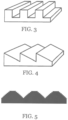
- the pattern is a sinusoidal pattern, a squared pattern, or a triangular pattern, some of which are shown as examples in Figures 3 and 5 .
- Figure 6 schematically illustrates incident light 4 incoming on a periodic diffractive grating 3 of a waveguide 1.
- the incident angle ⁇ of the incident light beam is defined as the angle between the average normal N of the surface and the projection of the beam of light on a plane 6, which is perpendicular to the grating orientation 7.
- the plane 6 is not part of the invention.
- the grating comprises a repetition of shapes, which are repeated along a direction perpendicular to the grating orientation 7.
- Figures 7 and 8 schematically illustrate the incident light 4 incoming on a periodic diffractive grating of a waveguide 1.
- Figure 7 and 8 illustrate the influence of the waveguide thickness WT on the transmission of the light.
- the waveguide comprises a section (11) designed to transmit the light by total internal reflections 12, and when the purpose of the grating is to couple the light into said section 11, the thickness WT is optimized such as to maximize the amount of light that reaches said section 11; the overall coupling efficiency may be defined as the ratio between one given mode, for example +1 or -1, of the coupled light 14 into said section 11 and the incident light 4 at a given wavelength. If the thickness is not optimally set, like in Figures 7 , part of the light 10 gets decoupled from the waveguide before reaching the section of the waveguide 11 which guides the light by internal reflections. This decoupling results in a loss of the overall coupling efficiency.
- the coupling efficiency may be defined as the ratio between one given mode, for example +1 or -1, of the coupled light 13, which is the light that managed to cross the grating, and the incident light 4 at a given wavelength.
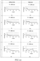
- Figure 11 illustrates the coupling efficiency Ce of an incident light impinging on the grating with an angle ⁇ , for the diffraction order 1 (T1) - in cells A1, B1 and C1-and diffraction order -1 (T-1)-in cells A2, B2 and C2 for a device obtained by a method according to claim 1.
- the grating depth d is 210nm
- the grating period P is 380nm.
- the refraction index of the waveguide n3 is 1.5.
- FIG. 11 also illustrates that the method according to claim 6 can be applied by defining two target efficiency distributions in a setup according to the top of Figure 14 : a target efficiency can be defined for order +1, another target efficiency can be defined for order -1; the order +1 is coupled toward the right of the waveguide, order -1 is coupled toward the left of the waveguide; the difference between the target efficiency and the computed efficiency being the sum of the differences for each mode taken separately.
- Said setup can be used to split the light according to its wavelength.
- Figure 12 shows the coupling efficiency Ce for different incident angles ⁇ or a device obtained by the method according to claim 3.
- the grating depth d is 210nm
- the grating period P is 380nm.
- the refraction index of the waveguide n3 is 1.5.
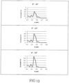
- Figure 13 combines the results of Figure 12 , using the same waveguide and grating to show the coupling efficiency of a non-collimated incident light beam.
- the Figure shows, for example, that the coupling efficiency can reach 80% even if the incident angle ⁇ of the input light beam varies from 4° to 12°, and can reach 90% if said angle is comprised between 6° and 10°.
- a collimated light beam has a small standard deviation S ⁇ , as found in lasers with a beam divergence S ⁇ of 1 to 2 mrad, whereas a non-collimated beam has a large standard deviation S ⁇ .
- Figure 14 show the influence of the grating period P on the coupling efficiency as a function of wavelength w for a normal incident light beam on a device obtained according to the method of claim 1.
- the figure shows the diffraction order 1 (16) and the diffraction order -1 (15), which for a normal incident beam have the same coupling performance. It shows a setup where a wavefront 20 is coupled into the waveguide according to the invention through a first grating 21 and decoupled through two gratings 22. It shows that the grating can be used as a spectral filter.
- Figure 15 show the influence of the grating period P on the coupling efficiency as a function of wavelength w for an incident light beam at 8° for a device obtained by the method according to claim 1, i.e. the method described above for a light coupling system with a rectangular pattern and with an enhancement layer.
- the depth d of the grating is 200nm.
- the refraction index n3 of the grating is 1.5.
- the angle of the incident light with the surface normal vector ⁇ is 8°. Longer periods P shift the coupling efficiency to the red and infrared part of the spectrum.
- Figure 16 shows a setup where a wavefront 20 is coupled into the waveguide through a first grating 21 and decoupled through a second grating 22. This setup can be used to transmit an image of an object located in front of grating 21 to a remote sensor located in front of grating 22 and sensibly reduces the required free space that would be necessary in a conventional imaging situation.
- Figure 19 shows the coupling efficiency Ce of a grating and waveguide during the optimization of the second set of parameters of the grating in the method according to claim 1.
- the optimization step minimizes the sum at every wavelength comprised between 360nm and 830nm of the squared differences between the computed coupling efficiency and the target efficiency.
- the grating shape is rectangular with a fill factor of 50%.
- the grating is coated with an enhancement layer of ZnS.
- the grating period P is constrained between 250nm and 1000nm, the grating depth d is constrained between mm and 400nm.
- the enhancement layer thickness L is constrained between mm and 250nm.
- the incident angle ⁇ is constrained between 0° and 10°, and its standard deviation S ⁇ is set to 0.5°.
- Figure 20 shows the evolution of the sum of squared difference between the target efficiency and the computed efficiency as a function of the iteration step in the optimization setup referred by Figure 19 .
- a parameter of the first parameter set according to this invention is not known a-priori, the method according to this invention can be applied for several choices of said parameter, and the best result, i.e. the one that results in the minimal difference between the target efficiency and the computed efficiency, is found by trial-and-error.
- Figure 21 and 22 show the coupling efficiency Ce for the first diffraction order obtained by a method, not being part of the invention, for a light coupling system with a rectangular pattern with an uncoated grating.
- the target wavelength is a Gaussian with a mean value of 500nm and a standard deviation of 30nm.
- the incident angle ⁇ is constrained between -40° and 40°.
- the grating is rectangular shaped.
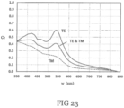
- Figure 23 shows the coupling efficiency Ce for the first diffraction order obtained by a method, not being part of the invention, with an uncoated grating.
- the target wavelength is a Gaussian with a mean value of 532nm and a standard deviation of 30nm.
- the incident angle ⁇ is constrained between -40° and 40°.
- the grating is rectangular shaped.
- Figure 23 shows the resulting coupling efficiency for TE, TM and TE&TM, but performs the optimization for both polarizations TE&TM, which is the equivalent of performing an optimization for unpolarized light.
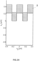
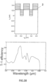
- Fig.24 shows a typical ZnS enhancement coating used for the efficient coupling of unpolarized light.
- Figures 25 to 30 show more results obtained by the optimization method for different wavelengths, different incidence angles and for unpolarized light.
- the structures obtained are optimized for unpolarized light and are therefore optimized for any incident light beam, having only one polarization, any linear polarization, a circular or ellipsoidal polarization and any time-dependent or position-dependent polarization.
- Figure 25 shows a ZnS enhancement coating optimized for an incidence angle of 14° for blue (450-495nm) and unpolarized light, i.e. the TE and TM components of the incident light beam have the same amplitudes.
- the ZnS layer thickness is 240nm, evaporated on a 340nm period and 220nm deep, 0.56 fill factor grating realized on PC.
- Figure 26 shows a ZnS enhancement coating optimized for an incidence angle of 14° for green (460-485nm) and unpolarized light.
- the ZnS layer thickness is 280nm, evaporated on a 400nm period and 260nm deep, 0.54 fill factor grating realized on PC.
- Figure 27 shows a ZnS enhancement coating optimized for an incidence angle of 14° for red (600-640nm) and unpolarized light.
- the ZnS layer thickness is 300nm, evaporated on a 450nm period and 280nm deep, 0.56 fill factor grating realized on PC.
- Figure 28 shows a ZnS enhancement coating optimized for an incidence angle of 15° for blue-green-red and unpolarized light.
- the ZnS layer thickness is 240nm, evaporated on a 360nm period and 230nm deep, 0.66 fill factor grating realized on PC.
- Figure 29 shows the obtained efficiency in case of a sinusoidal grating for an incidence angle of 17° and for red (615-630nm), green (560-575nm) and blue (460-480nm).
- the sinusoidal depth of the sinusoidal grating ( Fig. 29 ) is smaller than 1 period, the period is 390nm, the ZnS coating thickness is 350nm and the ZnS coating is deposited on PC.
- the sinusoidal grating of Fig.29 is illuminated, the diffracted light beam has a flat spectrum in the visible range and appears white to an observer.
Landscapes
- Physics & Mathematics (AREA)
- General Physics & Mathematics (AREA)
- Optics & Photonics (AREA)
- Optical Integrated Circuits (AREA)
- Optical Couplings Of Light Guides (AREA)
Claims (12)
- Verfahren zum Herstellen eines Lichteinkopplungssystems, wobei ein Gitter (3) auf einer Oberfläche eines Mehrmoden-Wellenleiters (1) hergestellt wird, wobei das Gitter (3) den Lichteintritt des Mehrmoden-Wellenleiters (1) für einen einfallenden Lichtstrahl (4) definiert, wobei das Gitter (3) eine Wiederholung von Mustern umfasst, die jeweils eine Musterbreite und eine Musterlänge aufweisen, wobei die Muster entlang einer zur Musterlänge senkrechten Richtung wiederholt werden, wobei das Gitter eine Form aufweist, die in einer zur Musterlänge senkrechten Ebene definiert ist, ausgewählt aus einer rechteckigen Form, einer sinusförmigen Form, einer dreieckigen Form oder einer Treppenform,wobei das Verfahren einen Schritt des Auswählens eines ersten Parametersatzes umfasst, umfassend:• Wellenlängenverteilung des einfallenden Lichts (4), das durch den Mehrmoden-Wellenleiter übertragen werden soll,• polarisierte oder unpolarisierte Natur des einfallenden Lichts,• die Standardabweichung SΘ des Einfallswinkels Θ von einfallendem Licht (4) zum Mehrmoden-Wellenleiter (1), wobei der Einfallswinkel Θ als der Winkel zwischen der durchschnittlichen Normalen N der Oberfläche und der Projektion des Lichtstrahls auf eine Ebene definiert ist, die senkrecht zur Musterlängenausrichtung ist,• Form der Muster, die derart gestaltet ist, dass ihre lokale Flächennormale Ns an jeder Stelle der Form einen Winkel α zur durchschnittlichen Normalen N der Oberfläche bildet, wobei der Winkel a zwischen α=-90° und α=90° liegt,• Brechungsindex n1 des den Mehrmoden-Wellenleiter umgebenden Mediums,• einen Brechungsindex n3 des Mehrmoden-Wellenleiters,wobei das Verfahren einen Schritt des Auswählens eines zweiten Parametersatzes umfasst, umfassend:• Gitterperiode P, die zwei benachbarte Muster trennt,• Gittertiefe d zwischen dem höchsten und dem niedrigsten Punkt des Musters,• mittlerer Einfallswinkel θ des einfallenden Lichts (4) zum Mehrmoden-Wellenleiter,wobei das Verfahren einen Schritt des Optimierens des zweiten Parametersatzes umfasst, um einen optimierten zweiten Parametersatz zu erhalten, und die folgenden Schritte umfasst:• Definieren einer Zieleffizienz, die als Eingangsverteilung in Bezug auf die Wellenlänge des einfallenden Lichts (4) gegeben ist,• Berechnen der Effizienz in Bezug auf die Wellenlänge des einfallenden Lichts (4) auf der Grundlage des ersten und des zweiten Parametersatzes,• Minimieren der Differenz zwischen der Zieleffizienz und der berechneten Effizienz durch Ändern jedes Parameters des zweiten Parametersatzes,wobei der Optimierungsschritt ausgeführt wird, um eine Übertragungseffizienz Ce des einfallenden Lichts (4), das durch das Gitter (3) in den Mehrmoden-Wellenleiter (1) eintritt, für die erste oder die zweite Beugungsordnung zu erhalten, die bei einer gegebenen Wellenlänge des einfallenden Lichts (4) 35% bei unpolarisiertem Licht übersteigt oder 50% bei polarisiertem Licht übersteigt,wobei das Gitter (3) eine entlang der zur Musterlänge senkrechten Richtung gemessene Gitterlänge D aufweist, wobei die Gitterlänge D mit der Dicke WT des Mehrmoden-Wellenleiters und dem Winkel β zwischen der durchschnittlichen Normalen des Mehrmoden-Wellenleiters und dem Lichtstrahl (14) innerhalb des Mehrmoden-Wellenleiters in Beziehung steht, wobei die Länge D durch die folgende Ungleichung definiert ist:
 wobei das Verfahren einen Schritt des Herstellens des Gitters (3) auf der Oberfläche des Mehrmoden-Wellenleiters gemäß dem gewählten ersten Parametersatz und dem optimierten zweiten Parametersatz umfasst, wobei das Gitter (3) mit einer Verstärkungsschicht (2) bedeckt ist, deren Brechungsindex n2 zum ersten Parametersatz gehört und deren Dicke L zum zweiten Parametersatz gehört, wobei die Verstärkungsschicht (2) eine Form aufweist, die der Form der Muster entspricht, und eine Dicke L zwischen 10nm und 500nm, vorzugsweise zwischen 10nm und 200nm, aufweist,
und wobeider Optimierungsschritt das Optimieren der Schichtdicke L umfasst und n2-n1 größer oder gleich 0,3, vorzugsweise größer oder gleich 0,5, vorzugsweise größer oder gleich 0,8 ist, undn2-n3 größer oder gleich 0,3, vorzugsweise größer oder gleich 0,5, vorzugsweise größer oder gleich 0,8 ist, wobei, wenn die Form des Musters rechteckig ist, der Optimierungsschritt ferner das Optimieren des Rechteckige Füllfaktors A/P umfasst, der als die Breite eines Rechtecks A im Vergleich zur Gitterperiode P definiert ist. - Verfahren nach Anspruch 1, wobei die Verstärkungsschicht (2) aus einem Material besteht, das aus ZnS oder TiO2 oder HfO2 oder Ta2O5 oder ZrO2 oder AlN oder Al2O3 oder ZnO oder einer Kombination dieser Materialien ausgewählt ist.
- Verfahren nach Anspruch 1, wobei der Optimierungsschritt dazu gestaltet ist, eine Übertragungseffizienz des einfallenden Lichts (4) in den Wellenleiter (1) für die erste oder die zweite Beugungsordnung zu erhalten, die bei einer gegebenen Wellenlänge des einfallenden Lichts 50% übersteigt, vorzugsweise 70% übersteigt, vorzugsweise 90% übersteigt.
- Optisches System, umfassend ein Lichteinkopplungssystem, das durch ein Verfahren nach einem der Ansprüche 1 bis 3 zum Einkoppeln eines polarisierten oder unpolarisierten einfallenden Lichtstrahls (4) in einen Mehrmoden-Wellenleiter (1) erhalten werden kann, und eine Lichteingangskomponente, die dazu eingerichtet ist, den Lichtstrahl für ein Gitter (3) des Mehrmoden-Wellenleiters (1) bereitzustellen, wobei der Lichtstrahl (4) eine gegebene Wellenlängenverteilung aufweist und das optische System in ein Medium mit Brechungsindex n1 eingetaucht ist, wobei das Lichteinkopplungssystem umfasst:• den Mehrmoden-Wellenleiter (1) mit einem Brechungsindex n3,• das auf einer Oberfläche des Mehrmoden-Wellenleiters (1) hergestellte Gitter zum Einkoppeln des Lichtstrahls (4) in den Mehrmoden-Wellenleiter, wobei das Gitter eine Lichteintrittsfläche definiert und eine Gitterperiode P und eine Gittertiefe d umfasst,wobei:das Gitter (3) eine Wiederholung von Mustern mit einer Form umfasst, die ihre eigene lokale Flächennormale Ns an jeder Stelle der Form aufweist, die einen Winkel α zur durchschnittlichen Normalen N der Oberfläche des Mehrmoden-Wellenleiters bildet, wobei der Winkel α zwischen α=-90° und α=90° liegt, wobei die Gittertiefe d zwischen dem höchsten und dem niedrigsten Punkt der Muster definiert ist, und wobei die Form aus einer rechteckigen Form, einer sinusförmigen Form, einer dreieckigen Form oder einer Treppenform ausgewählt ist,das Gitter eine auf der Oberfläche in Richtung des gebeugten Strahls gemessene Länge D aufweist, wobei die Länge D mit der Dicke WT des Mehrmoden-Wellenleiters (1) und dem Winkel β zwischen der Normalen der Oberfläche des Mehrmoden-Wellenleiters und einem Lichtstrahl (14) innerhalb des Mehrmoden-Wellenleiters (1) in Beziehung steht, wobei die Länge D durch die folgende Ungleichung definiert ist:
 das Lichteinkopplungssystem eine das Gitter (3) bedeckende Verstärkungsschicht (2) umfasst, die einen Brechungsindex n2 aufweist und aus einem Material besteht, das aus ZnS oder TiO2 oder HfO2 oder Ta2O5 oder ZrO2 oder AlN oder Al2O3 oder ZnO oder einer Kombination dieser Materialien ausgewählt ist, wobei die Verstärkungsschicht (2) eine der Form der Muster entsprechende Form aufweist und• wobei n2-n1 größer oder gleich 0,3, vorzugsweise größer oder gleich 0,5, vorzugsweise größer oder gleich 0,8 ist, und• wobei n2-n3 größer oder gleich 0,3, vorzugsweise größer oder gleich 0,5, vorzugsweise größer oder gleich 0,8 ist, undwobei die Dicke L der Verstärkungsschicht (2) auf dem Gitter (3) zwischen 10nm und 500nm, vorzugsweise zwischen 10nm und 200nm, beträgt, wobei das Lichteinkopplungssystem eine Übertragungseffizienz Ce des einfallenden Lichtstrahls (4) in den Mehrmoden-Wellenleiter (3) für die erste oder die zweite Beugungsordnung bietet, die bei unpolarisiertem Licht bei einer gegebenen Wellenlänge des einfallenden Lichtstrahls 35% übersteigt oder bei polarisiertem Licht bei einer gegebenen Wellenlänge des einfallenden Lichtstrahls (4) 50% übersteigt, vorzugsweise 70% übersteigt, vorzugsweise 90% übersteigt, wobei, wenn die Form des Musters rechteckig ist, der Füllfaktor A/P, der als die Breite eines Rechtecks A im Vergleich zur Gitterperiode P definiert ist, zwischen 10% und 90%, vorzugsweise zwischen 40% und 60%, beträgt.
 - Optisches System nach Anspruch 4, wobei der Mehrmoden-Wellenleiter (1) aus Glas oder Quarz oder Polymer oder Sol-Gel besteht.
- Optisches System nach Anspruch 4, wobei der Mehrmoden-Wellenleiter (1) aus Polycarbonat PC oder Polymethylmethacrylat PMMA oder Polyethylenterephthalat PET besteht.
- Optisches System nach einem der Ansprüche 4 bis 6, wobei die Gittertiefe d zwischen dem höchsten und dem niedrigsten Punkt des Gittermusters zwischen 10nm und 1000nm, vorzugsweise zwischen 20nm und 400nm, beträgt.
- Optisches System nach einem der Ansprüche 4 bis 7, wobei das Gitter auf der oberen Oberfläche des Wellenleiters hergestellt ist und wobei die Wellenleiterdicke WT größer oder gleich 1 Mikrometer, vorzugsweise größer oder gleich 10 Mikrometer, vorzugsweise größer oder gleich 0,5 mm, ist.
- Optisches System nach einem der Ansprüche 4 bis 8, wobei die Dicke L der Verstärkungsschicht (2) zwischen 100nm und 200nm beträgt.
- Optisches System nach einem der Ansprüche 4 bis 9 zum Einkoppeln des einfallenden Lichtstrahls (4) mit einer Wellenlänge zwischen 400nm und 700nm, wobei die Gitterperiode P, die zwei benachbarte Muster trennt, zwischen 230nm und 840nm beträgt.
- Optisches System nach einem der Ansprüche 4 bis 9 zum Einkoppeln des einfallenden Lichtstrahls (4) mit einer Wellenlänge zwischen 700nm und 2500nm, wobei die Gitterperiode P, die zwei benachbarte Muster trennt, zwischen 580nm und 3000nm beträgt.
- Optisches System nach einem der Ansprüche 4 bis 9 zum Einkoppeln des einfallenden Lichtstrahls (4) mit einer Wellenlänge zwischen 250nm und 400nm, wobei die Gitterperiode P, die zwei benachbarte Muster trennt, zwischen 180nm und 560nm beträgt.
Priority Applications (1)
| Application Number | Priority Date | Filing Date | Title |
|---|---|---|---|
| EP13739739.4A EP2877884B1 (de) | 2012-07-25 | 2013-07-24 | Verfahren zur optimierung eines optischen einkoppelwellenleiters |
Applications Claiming Priority (3)
| Application Number | Priority Date | Filing Date | Title |
|---|---|---|---|
| EP2012064634 | 2012-07-25 | ||
| PCT/EP2013/065631 WO2014016343A2 (en) | 2012-07-25 | 2013-07-24 | Method to optimize a light coupling waveguide |
| EP13739739.4A EP2877884B1 (de) | 2012-07-25 | 2013-07-24 | Verfahren zur optimierung eines optischen einkoppelwellenleiters |
Publications (2)
| Publication Number | Publication Date |
|---|---|
| EP2877884A2 EP2877884A2 (de) | 2015-06-03 |
| EP2877884B1 true EP2877884B1 (de) | 2024-11-27 |
Family
ID=52997779
Family Applications (1)
| Application Number | Title | Priority Date | Filing Date |
|---|---|---|---|
| EP13739739.4A Active EP2877884B1 (de) | 2012-07-25 | 2013-07-24 | Verfahren zur optimierung eines optischen einkoppelwellenleiters |
Country Status (1)
| Country | Link |
|---|---|
| EP (1) | EP2877884B1 (de) |
Families Citing this family (3)
| Publication number | Priority date | Publication date | Assignee | Title |
|---|---|---|---|---|
| US10197804B2 (en) * | 2016-04-25 | 2019-02-05 | Microsoft Technology Licensing, Llc | Refractive coating for diffractive optical elements |
| EP3588142A1 (de) | 2018-06-25 | 2020-01-01 | IRIS Industries SA | Lidar mit mehreren wellenlängen |
| CN112639575A (zh) | 2018-09-07 | 2021-04-09 | 华为技术有限公司 | 用于增强现实的高折射率波导 |
Citations (3)
| Publication number | Priority date | Publication date | Assignee | Title |
|---|---|---|---|---|
| EP0982071A1 (de) * | 1998-08-28 | 2000-03-01 | Sony Corporation | Photokatalytische Vorrichtung mit Anregung |
| JP3100499B2 (ja) * | 1993-11-25 | 2000-10-16 | シャープ株式会社 | グレーティングカップラーおよびこれを有する光導波路素子 |
| US20100277803A1 (en) * | 2006-12-14 | 2010-11-04 | Nokia Corporation | Display Device Having Two Operating Modes |
-
2013
- 2013-07-24 EP EP13739739.4A patent/EP2877884B1/de active Active
Patent Citations (3)
| Publication number | Priority date | Publication date | Assignee | Title |
|---|---|---|---|---|
| JP3100499B2 (ja) * | 1993-11-25 | 2000-10-16 | シャープ株式会社 | グレーティングカップラーおよびこれを有する光導波路素子 |
| EP0982071A1 (de) * | 1998-08-28 | 2000-03-01 | Sony Corporation | Photokatalytische Vorrichtung mit Anregung |
| US20100277803A1 (en) * | 2006-12-14 | 2010-11-04 | Nokia Corporation | Display Device Having Two Operating Modes |
Non-Patent Citations (3)
| Title |
|---|
| JANYCE FRANC ET AL: "High-efficiency diffraction grating coupler for multimode optical interconnect", PROCEEDINGS OF SPIE, vol. 6185, 21 April 2006 (2006-04-21), US, pages 61851F-1, XP040223274, ISBN: 978-1-5106-1533-5, DOI: 10.1117/12.666710 * |
| MILLER J M ET AL: "DESIGN AND FABRICATION OF BINARY SLANTED SURFACE-RELIEF GRATINGS FOR A PLANAR OPTICAL INTERCONNECTION", APPLIED OPTICS, OPTICAL SOCIETY OF AMERICA, WASHINGTON, DC, US, vol. 36, no. 23, 10 August 1997 (1997-08-10), pages 5717 - 5727, XP000699467, ISSN: 0003-6935, DOI: 10.1364/AO.36.005717 * |
| TAPANI LEVOLA ET AL: "Replicated slanted gratings with a high refractive index material for in and outcoupling of light", OPTICS EXPRESS, OSA PUBLISHING, US, vol. 15, no. 5, 5 March 2007 (2007-03-05), pages 2067 - 2074, XP002624810, ISSN: 1094-4087, DOI: 10.1364/OE.15.002067 * |
Also Published As
| Publication number | Publication date |
|---|---|
| EP2877884A2 (de) | 2015-06-03 |
Similar Documents
| Publication | Publication Date | Title |
|---|---|---|
| US9739950B2 (en) | Method to optimize a light coupling waveguide | |
| CN110596807B (zh) | 波导结构、显示装置及电子设备 | |
| CN103097930B (zh) | 取光板和棒以及使用了它们的光接收装置和发光装置 | |
| US6661952B2 (en) | Sub-wavelength efficient polarization filter (SWEP filter) | |
| CN103270442B (zh) | 取光板和棒以及使用了它们的光接收装置和发光装置 | |
| KR20200069335A (ko) | 증강 현실 시스템을 위한 도파관-기반 광학 시스템 및 방법 | |
| CN115343795B (zh) | 一种衍射光波导及成像系统 | |
| EP4471470A1 (de) | Gestapeltes gitter und ar-anzeigevorrichtung | |
| US20040047039A1 (en) | Wide angle optical device and method for making same | |
| EP1506440A2 (de) | Planarer optischer wellenleiter | |
| CN103999303A (zh) | 集成亚波长光栅系统 | |
| CN218956846U (zh) | 一种衍射光波导及近眼显示设备 | |
| CN115469393B (zh) | 衍射光波导及ar眼镜 | |
| TW202238191A (zh) | 顯示結構及顯示裝置 | |
| CN114527536A (zh) | 一种光波导及其制作方法、抬头显示器 | |
| EP2877884A2 (de) | Verfahren zur optimierung eines optischen einkoppelwellenleiters | |
| KR20100126720A (ko) | Mems 기반 펠리클 빔스플리터 | |
| CN118068474A (zh) | 光波导及ar显示设备 | |
| CN115236788A (zh) | 光波导器件、近眼显示装置以及智能眼镜 | |
| CN118962887B (zh) | 光波导及近眼显示设备 | |
| JP2001296438A (ja) | フォトブリーチング導波路 | |
| Wang et al. | High-precision inverse design of multi-category grating couplers based on KAN-transformer | |
| FI131617B1 (en) | DISPLAY STRUCTURE | |
| CN100356217C (zh) | 光合波/分波器及其制造方法 | |
| Ranacher et al. | Design of a mid-infrared bandpass filter with large rejection bandwidth for silicon photonics |
Legal Events
| Date | Code | Title | Description |
|---|---|---|---|
| PUAI | Public reference made under article 153(3) epc to a published international application that has entered the european phase |
Free format text: ORIGINAL CODE: 0009012 |
|
| 17P | Request for examination filed |
Effective date: 20150123 |
|
| AK | Designated contracting states |
Kind code of ref document: A2 Designated state(s): AL AT BE BG CH CY CZ DE DK EE ES FI FR GB GR HR HU IE IS IT LI LT LU LV MC MK MT NL NO PL PT RO RS SE SI SK SM TR |
|
| AX | Request for extension of the european patent |
Extension state: BA ME |
|
| RIN1 | Information on inventor provided before grant (corrected) |
Inventor name: STALDER, MARTIN Inventor name: PIRES, DAVID Inventor name: SQALLI, OMAR Inventor name: BASSET, GUILLAUME |
|
| DAX | Request for extension of the european patent (deleted) | ||
| STAA | Information on the status of an ep patent application or granted ep patent |
Free format text: STATUS: EXAMINATION IS IN PROGRESS |
|
| 17Q | First examination report despatched |
Effective date: 20200716 |
|
| GRAP | Despatch of communication of intention to grant a patent |
Free format text: ORIGINAL CODE: EPIDOSNIGR1 |
|
| STAA | Information on the status of an ep patent application or granted ep patent |
Free format text: STATUS: GRANT OF PATENT IS INTENDED |
|
| INTG | Intention to grant announced |
Effective date: 20240809 |
|
| GRAS | Grant fee paid |
Free format text: ORIGINAL CODE: EPIDOSNIGR3 |
|
| GRAA | (expected) grant |
Free format text: ORIGINAL CODE: 0009210 |
|
| STAA | Information on the status of an ep patent application or granted ep patent |
Free format text: STATUS: THE PATENT HAS BEEN GRANTED |
|
| AK | Designated contracting states |
Kind code of ref document: B1 Designated state(s): AL AT BE BG CH CY CZ DE DK EE ES FI FR GB GR HR HU IE IS IT LI LT LU LV MC MK MT NL NO PL PT RO RS SE SI SK SM TR |
|
| REG | Reference to a national code |
Ref country code: GB Ref legal event code: FG4D |
|
| REG | Reference to a national code |
Ref country code: CH Ref legal event code: EP |
|
| REG | Reference to a national code |
Ref country code: DE Ref legal event code: R096 Ref document number: 602013086322 Country of ref document: DE |
|
| REG | Reference to a national code |
Ref country code: IE Ref legal event code: FG4D |
|
| REG | Reference to a national code |
Ref country code: LT Ref legal event code: MG9D |
|
| REG | Reference to a national code |
Ref country code: NL Ref legal event code: MP Effective date: 20241127 |
|
| PG25 | Lapsed in a contracting state [announced via postgrant information from national office to epo] |
Ref country code: IS Free format text: LAPSE BECAUSE OF FAILURE TO SUBMIT A TRANSLATION OF THE DESCRIPTION OR TO PAY THE FEE WITHIN THE PRESCRIBED TIME-LIMIT Effective date: 20250327 Ref country code: HR Free format text: LAPSE BECAUSE OF FAILURE TO SUBMIT A TRANSLATION OF THE DESCRIPTION OR TO PAY THE FEE WITHIN THE PRESCRIBED TIME-LIMIT Effective date: 20241127 Ref country code: PT Free format text: LAPSE BECAUSE OF FAILURE TO SUBMIT A TRANSLATION OF THE DESCRIPTION OR TO PAY THE FEE WITHIN THE PRESCRIBED TIME-LIMIT Effective date: 20250327 |
|
| PG25 | Lapsed in a contracting state [announced via postgrant information from national office to epo] |
Ref country code: FI Free format text: LAPSE BECAUSE OF FAILURE TO SUBMIT A TRANSLATION OF THE DESCRIPTION OR TO PAY THE FEE WITHIN THE PRESCRIBED TIME-LIMIT Effective date: 20241127 Ref country code: NL Free format text: LAPSE BECAUSE OF FAILURE TO SUBMIT A TRANSLATION OF THE DESCRIPTION OR TO PAY THE FEE WITHIN THE PRESCRIBED TIME-LIMIT Effective date: 20241127 |
|
| REG | Reference to a national code |
Ref country code: AT Ref legal event code: MK05 Ref document number: 1746211 Country of ref document: AT Kind code of ref document: T Effective date: 20241127 |
|
| PG25 | Lapsed in a contracting state [announced via postgrant information from national office to epo] |
Ref country code: BG Free format text: LAPSE BECAUSE OF FAILURE TO SUBMIT A TRANSLATION OF THE DESCRIPTION OR TO PAY THE FEE WITHIN THE PRESCRIBED TIME-LIMIT Effective date: 20241127 |
|
| PG25 | Lapsed in a contracting state [announced via postgrant information from national office to epo] |
Ref country code: ES Free format text: LAPSE BECAUSE OF FAILURE TO SUBMIT A TRANSLATION OF THE DESCRIPTION OR TO PAY THE FEE WITHIN THE PRESCRIBED TIME-LIMIT Effective date: 20241127 |
|
| PG25 | Lapsed in a contracting state [announced via postgrant information from national office to epo] |
Ref country code: NO Free format text: LAPSE BECAUSE OF FAILURE TO SUBMIT A TRANSLATION OF THE DESCRIPTION OR TO PAY THE FEE WITHIN THE PRESCRIBED TIME-LIMIT Effective date: 20250227 |
|
| PG25 | Lapsed in a contracting state [announced via postgrant information from national office to epo] |
Ref country code: LV Free format text: LAPSE BECAUSE OF FAILURE TO SUBMIT A TRANSLATION OF THE DESCRIPTION OR TO PAY THE FEE WITHIN THE PRESCRIBED TIME-LIMIT Effective date: 20241127 Ref country code: AT Free format text: LAPSE BECAUSE OF FAILURE TO SUBMIT A TRANSLATION OF THE DESCRIPTION OR TO PAY THE FEE WITHIN THE PRESCRIBED TIME-LIMIT Effective date: 20241127 Ref country code: GR Free format text: LAPSE BECAUSE OF FAILURE TO SUBMIT A TRANSLATION OF THE DESCRIPTION OR TO PAY THE FEE WITHIN THE PRESCRIBED TIME-LIMIT Effective date: 20250228 |
|
| PG25 | Lapsed in a contracting state [announced via postgrant information from national office to epo] |
Ref country code: PL Free format text: LAPSE BECAUSE OF FAILURE TO SUBMIT A TRANSLATION OF THE DESCRIPTION OR TO PAY THE FEE WITHIN THE PRESCRIBED TIME-LIMIT Effective date: 20241127 |
|
| PG25 | Lapsed in a contracting state [announced via postgrant information from national office to epo] |
Ref country code: RS Free format text: LAPSE BECAUSE OF FAILURE TO SUBMIT A TRANSLATION OF THE DESCRIPTION OR TO PAY THE FEE WITHIN THE PRESCRIBED TIME-LIMIT Effective date: 20250227 |
|
| PG25 | Lapsed in a contracting state [announced via postgrant information from national office to epo] |
Ref country code: SM Free format text: LAPSE BECAUSE OF FAILURE TO SUBMIT A TRANSLATION OF THE DESCRIPTION OR TO PAY THE FEE WITHIN THE PRESCRIBED TIME-LIMIT Effective date: 20241127 |
|
| PG25 | Lapsed in a contracting state [announced via postgrant information from national office to epo] |
Ref country code: DK Free format text: LAPSE BECAUSE OF FAILURE TO SUBMIT A TRANSLATION OF THE DESCRIPTION OR TO PAY THE FEE WITHIN THE PRESCRIBED TIME-LIMIT Effective date: 20241127 |
|
| PG25 | Lapsed in a contracting state [announced via postgrant information from national office to epo] |
Ref country code: EE Free format text: LAPSE BECAUSE OF FAILURE TO SUBMIT A TRANSLATION OF THE DESCRIPTION OR TO PAY THE FEE WITHIN THE PRESCRIBED TIME-LIMIT Effective date: 20241127 |
|
| PG25 | Lapsed in a contracting state [announced via postgrant information from national office to epo] |
Ref country code: RO Free format text: LAPSE BECAUSE OF FAILURE TO SUBMIT A TRANSLATION OF THE DESCRIPTION OR TO PAY THE FEE WITHIN THE PRESCRIBED TIME-LIMIT Effective date: 20241127 |
|
| PG25 | Lapsed in a contracting state [announced via postgrant information from national office to epo] |
Ref country code: SK Free format text: LAPSE BECAUSE OF FAILURE TO SUBMIT A TRANSLATION OF THE DESCRIPTION OR TO PAY THE FEE WITHIN THE PRESCRIBED TIME-LIMIT Effective date: 20241127 |
|
| PG25 | Lapsed in a contracting state [announced via postgrant information from national office to epo] |
Ref country code: CZ Free format text: LAPSE BECAUSE OF FAILURE TO SUBMIT A TRANSLATION OF THE DESCRIPTION OR TO PAY THE FEE WITHIN THE PRESCRIBED TIME-LIMIT Effective date: 20241127 |
|
| PG25 | Lapsed in a contracting state [announced via postgrant information from national office to epo] |
Ref country code: IT Free format text: LAPSE BECAUSE OF FAILURE TO SUBMIT A TRANSLATION OF THE DESCRIPTION OR TO PAY THE FEE WITHIN THE PRESCRIBED TIME-LIMIT Effective date: 20241127 |
|
| REG | Reference to a national code |
Ref country code: DE Ref legal event code: R097 Ref document number: 602013086322 Country of ref document: DE |
|
| PG25 | Lapsed in a contracting state [announced via postgrant information from national office to epo] |
Ref country code: SE Free format text: LAPSE BECAUSE OF FAILURE TO SUBMIT A TRANSLATION OF THE DESCRIPTION OR TO PAY THE FEE WITHIN THE PRESCRIBED TIME-LIMIT Effective date: 20241127 |
|
| PLBE | No opposition filed within time limit |
Free format text: ORIGINAL CODE: 0009261 |
|
| STAA | Information on the status of an ep patent application or granted ep patent |
Free format text: STATUS: NO OPPOSITION FILED WITHIN TIME LIMIT |
|
| PGFP | Annual fee paid to national office [announced via postgrant information from national office to epo] |
Ref country code: DE Payment date: 20250722 Year of fee payment: 13 |
|
| PGFP | Annual fee paid to national office [announced via postgrant information from national office to epo] |
Ref country code: GB Payment date: 20250724 Year of fee payment: 13 |
|
| PGFP | Annual fee paid to national office [announced via postgrant information from national office to epo] |
Ref country code: FR Payment date: 20250723 Year of fee payment: 13 |
|
| PGFP | Annual fee paid to national office [announced via postgrant information from national office to epo] |
Ref country code: CH Payment date: 20250724 Year of fee payment: 13 |
|
| 26N | No opposition filed |
Effective date: 20250828 |
|
| PG25 | Lapsed in a contracting state [announced via postgrant information from national office to epo] |
Ref country code: LU Free format text: LAPSE BECAUSE OF NON-PAYMENT OF DUE FEES Effective date: 20250724 |
|
| REG | Reference to a national code |
Ref country code: BE Ref legal event code: MM Effective date: 20250731 |
|
| PG25 | Lapsed in a contracting state [announced via postgrant information from national office to epo] |
Ref country code: BE Free format text: LAPSE BECAUSE OF NON-PAYMENT OF DUE FEES Effective date: 20250731 |