EP2876829A1 - Dispositif et procédé d'extraction optique et dispositif optique d'insertion - Google Patents
Dispositif et procédé d'extraction optique et dispositif optique d'insertion Download PDFInfo
- Publication number
- EP2876829A1 EP2876829A1 EP14193427.3A EP14193427A EP2876829A1 EP 2876829 A1 EP2876829 A1 EP 2876829A1 EP 14193427 A EP14193427 A EP 14193427A EP 2876829 A1 EP2876829 A1 EP 2876829A1
- Authority
- EP
- European Patent Office
- Prior art keywords
- optical
- signal
- optical signal
- fourier transform
- pulse
- Prior art date
- Legal status (The legal status is an assumption and is not a legal conclusion. Google has not performed a legal analysis and makes no representation as to the accuracy of the status listed.)
- Granted
Links
- 230000003287 optical effect Effects 0.000 title claims abstract description 1048
- 238000000034 method Methods 0.000 title claims description 12
- 230000001360 synchronised effect Effects 0.000 claims abstract description 10
- 239000002612 dispersion medium Substances 0.000 claims description 72
- 239000002609 medium Substances 0.000 claims description 50
- 230000010287 polarization Effects 0.000 claims description 43
- 239000006185 dispersion Substances 0.000 claims description 15
- 230000000644 propagated effect Effects 0.000 claims description 13
- 230000003111 delayed effect Effects 0.000 claims description 7
- 239000000284 extract Substances 0.000 claims description 4
- 230000008569 process Effects 0.000 claims description 4
- 230000001131 transforming effect Effects 0.000 claims description 2
- 238000010586 diagram Methods 0.000 description 26
- 230000005540 biological transmission Effects 0.000 description 15
- 239000013307 optical fiber Substances 0.000 description 6
- 230000008859 change Effects 0.000 description 4
- 230000009466 transformation Effects 0.000 description 3
- 230000008033 biological extinction Effects 0.000 description 2
- 238000005516 engineering process Methods 0.000 description 2
- 230000010363 phase shift Effects 0.000 description 2
- 238000001228 spectrum Methods 0.000 description 2
- 230000005374 Kerr effect Effects 0.000 description 1
- 230000006835 compression Effects 0.000 description 1
- 238000007906 compression Methods 0.000 description 1
- 230000001934 delay Effects 0.000 description 1
- 230000006870 function Effects 0.000 description 1
- 239000004973 liquid crystal related substance Substances 0.000 description 1
- 230000004048 modification Effects 0.000 description 1
- 238000012986 modification Methods 0.000 description 1
- 238000012544 monitoring process Methods 0.000 description 1
- 230000001629 suppression Effects 0.000 description 1
Images


Classifications
-
- H—ELECTRICITY
- H04—ELECTRIC COMMUNICATION TECHNIQUE
- H04J—MULTIPLEX COMMUNICATION
- H04J14/00—Optical multiplex systems
- H04J14/08—Time-division multiplex systems
- H04J14/083—Add and drop multiplexing
-
- H—ELECTRICITY
- H04—ELECTRIC COMMUNICATION TECHNIQUE
- H04J—MULTIPLEX COMMUNICATION
- H04J14/00—Optical multiplex systems
- H04J14/02—Wavelength-division multiplex systems
- H04J14/0223—Conversion to or from optical TDM
-
- H—ELECTRICITY
- H04—ELECTRIC COMMUNICATION TECHNIQUE
- H04J—MULTIPLEX COMMUNICATION
- H04J14/00—Optical multiplex systems
- H04J14/02—Wavelength-division multiplex systems
- H04J14/0201—Add-and-drop multiplexing
- H04J14/0202—Arrangements therefor
- H04J14/021—Reconfigurable arrangements, e.g. reconfigurable optical add/drop multiplexers [ROADM] or tunable optical add/drop multiplexers [TOADM]
-
- H—ELECTRICITY
- H04—ELECTRIC COMMUNICATION TECHNIQUE
- H04Q—SELECTING
- H04Q11/00—Selecting arrangements for multiplex systems
- H04Q11/0001—Selecting arrangements for multiplex systems using optical switching
- H04Q11/0003—Details
Definitions
- the embodiments discussed herein are related to an optical drop device and an optical drop method by which an optical signal is dropped from a multi-channel optical signal, and an optical add device and an optical add method by which an optical signal is added to a multi-channel optical signal.
- WDM wavelength division multiplexing
- an optical add drop multiplexer (OADM) is provided in each node.
- the OADM may drop a specified optical signal from the WDM signal.
- the optical signal that is dropped from the WDM signal is guided, for example, to a client device.
- the OADM may add an optical signal that has been received from the client device or a further network, to the WDM signal.
- the above-described add/drop function of the OADM is realized, for example, using a wavelength selective switch (WSS).
- WSS may select an optical signal having a desired wavelength, for example, using an array waveguide grating, a micromachine, a liquid crystal, or the like.
- ROADM reconfigurable OADM
- the wavelength interval of the WDM signal When the wavelength interval of the WDM signal is reduced in the optical transmission system, the transmission capacity is further increased, and the flexibility of the network may be improved.
- it is difficult to realize sharp light-transmission characteristics, and there is a limitation of the wavelength intervals of a WDM signal.
- an optical drop device includes: a clock extractor configured to extract a clock signal from a multi-channel optical signal that includes a plurality of optical signals having different optical frequencies; a pulse generator configured to generate a pulse signal that is synchronized with the clock signal; an optical inverse Fourier transform unit configured to transform the multi-channel optical signal into a time division multiplexing optical signal by using an inverse Fourier transform; and an optical switch configured to drop an optical signal that exists in a time slot to which the pulse signal is applied, from the time division multiplexing optical signal.
- An OADM processes a WDM signal in which a plurality of optical signals having different wavelengths is multiplexed. That is, the OADM may drop an optical signal having a specified wavelength from the WDM signal. In addition, the OADM may add an optical signal having a certain wavelength to the WDM signal.
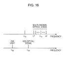
- a WDM signal may be referred to as a multi-channel optical signal.
- a plurality of channels may perform transmission of optical signals having different optical frequencies (or different wavelengths). That is, the multi-channel optical signal includes a plurality of optical signals having different optical frequencies.
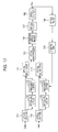
- FIG. 1 is a diagram illustrating a configuration of an OADM 1 according to an embodiment.
- the OADM 1 is used in an optical transmission system that performs transmission of a multi-channel optical signal S.
- the multi-channel optical signal S accommodates a plurality of channels v1 to vn.
- an optical frequency may be referred to as "frequency".
- the OADM 1 includes an optical drop device 2 and an optical add device 3.
- the optical drop device 2 may drop an optical signal having a desired frequency from an input multi-channel optical signal S IN .
- the optical drop device 2 drops an optical signal having a frequency vj from the input multi-channel optical signal S IN .
- the optical signal that has been dropped from the multi-channel optical signal S IN is guided, for example, to a client device as a drop optical signal S DROP -
- the multi-channel optical signal S IN from which the optical signal having the frequency vj has been dropped is guided to the optical add device 3 as a multi-channel optical signal S THRU ⁇ It is assumed that a channel vk of the multi-channel optical signal S THRU is not used.
- the multi-channel optical signal S THRU and an optical signal S ADD are input to the optical add device 3.
- the frequency of the optical signal S ADD is "vk”.
- the optical signal S ADD is generated, for example, by the client device.
- the optical add device 3 adds the optical signal S ADD to the multi-channel optical signal S THRU to generate a multi-channel optical signal S OUT .
- FIG. 1 a frequency spectrum of the input multi-channel optical signal SIN, the drop optical signal S DROP , the optical signal S ADD , and the multi-channel optical signal S OUT is illustrated.
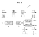
- FIG. 2 is a diagram illustrating a configuration of a first example of the optical drop device.
- an optical drop device 2A of the first example includes an optical inverse Fourier transform unit 11, an optical switch 12, an optical Fourier transform unit 13, and an optical Fourier transform unit 14.
- the optical signals having frequencies v1 to v4 may be respectively referred to as optical signals ⁇ 1 to ⁇ 4.
- frequency channels that are used to perform transmission of the optical signals v1 to v4 may be respectively referred to as the channels v1 to v4.
- FIG. 2 illustrates the frequency spectrum and strength of optical signals that are processed by the optical drop device 2A.
- the strength of an optical signal indicates a change in the strength or power of the optical signal within one symbol time.
- a multi-channel optical signal S IN is input to the optical inverse Fourier transform unit 11.
- the multi-channel optical signal S IN includes optical signals v1 to v4.
- the optical signals ⁇ 1 to ⁇ 4 are multiplexed in the frequency area.
- the optical inverse Fourier transform unit 11 transforms the multi-channel optical signal S IN into a time division multiplexing optical signal.
- the optical signals ⁇ 1 to v4 are respectively transformed into optical signals t1 to t4 by the optical inverse Fourier transform unit 11. That is, the time division multiplexing optical signal that has been generated from the multi-channel optical signal S IN includes the optical signals t1 to t4.
- the optical signals t1 to t4 are multiplexed in the time area.
- the time division multiplexing optical signal may be referred to a TDM optical signal.
- channels that are used to perform transmission of optical signals that are multiplexed in the TDM optical signal may be referred to as time slots. That is, in the TDM optical signal illustrated in FIG. 2 , the optical signals t1 to t4 may be multiplexed using time slots TS1 to TS4.
- the optical switch 12 may perform gate processing in the time area. That is, the optical switch 12 may drop a desired optical signal from the optical signals t1 to t4 that are multiplexed in the TDM optical signal. In the example illustrated in FIG. 2 , the optical switch 12 drops the optical signal t3 from the TDM optical signal. The optical signal t3 that has been dropped from the TDM optical signal is guided to the optical Fourier transform unit 14. On the other hand, the TDM optical signal from which the optical signal t3 has been dropped (that is, the TDM optical signal that includes the optical signals t1, t2, and t4) is guided to the optical Fourier transform unit 13. In the example illustrated in FIG. 2 , one optical signal is dropped from the TDM optical signal, but the optical switch 12 may drop a plurality of optical signals from the TDM optical signal.
- the optical Fourier transform unit 13 transforms the TDM optical signal that includes the optical signals t1, t2, and t4 into an optical signal in the frequency area. That is, the optical Fourier transform unit 13 executes transformation processing that corresponds to the optical inverse Fourier transform unit 11. As a result, the optical Fourier transform unit 13 generates a multi-channel optical signal S THRU that includes the optical signals v1, v2, and v4. The optical signals v1, v2, and ⁇ 4 are multiplexed in the frequency area.
- the optical Fourier transform unit 14 executes transformation processing that is the same as that of the optical Fourier transform unit 13, for the optical signal t3 that has been dropped from the TDM optical signal. That is, the optical Fourier transform unit 14 reproduces the optical signal v3.
- the optical drop device 2A transforms the multi-channel optical signal in the frequency area into the TDM optical signal in the time area, and executes optical drop by the gate processing in the time area. That is, the frequency intervals of the multi-channel optical signal (or wavelength intervals of the WDM signal) are transformed into the time intervals of the TDM optical signal.
- the gate processing in the time area may be speeded up sufficiently.
- the frequency intervals of the multi-channel optical signal may be narrowed practically.
- FIG. 3 is a diagram illustrating a configuration of a second example of the optical drop device.
- An optical drop device 2B of the second example includes an optical splitter 21, a clock extractor 22, a pulse generator 23, a modulator 24, a dispersion medium 25, an optical switch 26, a dispersion medium 27, a modulator 28, a dispersion medium 29, a modulator 30, an optical splitter 31, and a control unit 32.
- a multi-channel optical signal S IN includes a plurality of optical signals having different optical frequencies. It is desirable that dispersion that is applied to the multi-channel optical signal S IN in an optical transmission path (especially in chromatic dispersion) is compensated sufficiently.
- the OADM 1 illustrated in FIG. 1 may include a chromatic dispersion compensator on the input side of the optical drop device 2.
- the optical splitter 21 branches the multi-channel optical signal S IN and guides the multi-channel optical signals S IN to the clock extractor 22 and the modulator 24.
- the clock extractor 22 reproduces a clock from the multi-channel optical signal S IN and performs output of the clock signal.
- the clock signal is, for example, a sine curve voltage signal the voltage change of which is represented by a sine curve in the time area.
- the cycle of the clock signal is, for example, the same as a time that is assigned to one symbol that is transmitted by an optical signal.
- the pulse generator 23 generates a pulse signal that is synchronized with the clock signal.
- the width of a pulse in the pulse signal is, for example, about the same as one time slot of the TDM optical signal (time that is assigned to each of the optical signals that are multiplexed in the TDM optical signal).
- the pulse generator 23 generates an optical pulse signal or an electrical pulse signal. That is, when the optical switch 26 realizes the gate processing using an optical pulse, the pulse generator 23 generates an optical pulse signal from the clock signal. In addition, when the optical switch 26 realizes the gate processing using an electrical pulse, the pulse generator 23 generates an electrical pulse signal from the clock signal.
- the modulator 24 performs phase modulation on the multi-channel optical signal S IN using the clock signal.
- the modulator 24 may apply phase shift that corresponds to the voltage of the clock signal, to an input optical signal.
- the modulator 24 may further modulate the multi-channel optical signal S IN on which the phase modulation has been performed, using the clock signal, as appropriate.
- the dispersion medium 25 applies chromatic dispersion to the phase modulation multi-channel optical signal S IN that has been output from the modulator 24. As a result, a TDM optical signal is generated.
- the dispersion medium 25 is obtained, for example, by an optical fiber. In this case, a characteristic of the optical fiber (especially in a chromatic dispersion amount) and the length of the optical fiber are decided so that time slots of the generated TDM optical signal are arranged appropriately (alternatively, time intervals of a plurality of optical signals that are multiplexed in the generated TDM optical signal are arranged appropriately).
- FIG. 4 is a diagram illustrating the phase modulation by the modulator.
- a clock signal that is applied to the modulator 24 is adjusted so that the peak or minimum value of the voltage of the clock signal is located at the center of each symbol of the input optical signal.
- the N-th symbol of the input optical signal exists in a range of the times T1 to T3, the N-th symbol of the input optical signal exists.
- the timing of the clock signal is adjusted, for example, using a variable delay element that is not illustrated. It is desirable that the clock signal is adjusted so that the peak or minimum value of the voltage is located at the center of each symbol of the input optical signal, but the clock signal may be adjusted so that the peak or minimum value of the voltage is located at the approximate center of each of the symbols.
- the phase of lightwave by which the input optical signal is propagated is changed depending on the voltage.
- a phase shift amount of the lightwave is generally proportional to the drive voltage.
- the phase of the optical signal that has been output from the modulator 24 is changed in synchronization with the voltage of the clock signal.
- the phase amplitude of the optical signal that is output from the modulator 24 is proportional to the voltage amplitude of the clock signal.
- frequency chirp When the phase of the lightwave is changed, frequency chirp generally occurs.
- the frequency chirp is represented by time derivative of the phase (d ⁇ /dt).
- negative chirp occurs in the times T1 to T2
- positive chirp occurs in the times T2 to T3.
- the frequency chirp also becomes larger. That is, when the voltage amplitude of the clock signal is adjusted appropriately, desired frequency chirp can be obtained.
- the modulator 24 further performs intensity modulation on the phase modulation optical signal that has been obtained as described above.
- the modulator 24 includes a phase modulator and a strength modulator.
- the strength modulator is obtained, for example, by a Mach-Zehnder interferometer.
- the modulator 24 applies intensity modulation to the phase modulation optical signal depending on the voltage of the clock signal.
- the voltage amplitude of the clock signal is adjusted, for example, so as to be V ⁇ or less when the voltage amplitude is used for intensity modulation. Therefore, when the voltage of the clock signal is at a peak, the strength of the optical signal is also at a peak, and when the voltage of the clock signal is zero, the strength of the optical signal becomes almost zero.
- the phase modulation optical signal is transformed into an optical signal in which each symbol includes one pulse. That is, the intensity modulation by the clock signal is achieved.
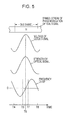
- FIG. 5 is a diagram illustrating the intensity modulation.
- the modulator 24 performs the intensity modulation so that a time area in which the frequency chirp of an optical signal is changed approximately linearly (linear chirp area) is extracted.
- the N-th symbol of the phase modulation optical signal exists in the times T4 to T8.
- the frequency chirp of the phase modulation optical signal is zero at the time T6, and is increased approximately linearly in the time period of the times T5 to T7.
- the modulator 24 performs the intensity modulation so that the optical signal in the time area that includes the time T6 is extracted.
- the above-described intensity modulation is achieved by adjusting timing of a clock signal that is applied to the strength modulator in the modulator 24. That is, the clock signal that is used for the intensity modulation is adjusted so that the peak of the voltage of the clock signal is located at the approximate center of each symbol in order to extract the linear chirp area.
- the optical signal that has been output from the modulator 24 is modulated so that the light strength of the linear chirp area becomes large and the light strength of a further time area becomes small.
- the intensity modulation is performed so that the light strength becomes at a peak when the frequency chirp is zero.
- the optical signal that has been output from the modulator 24 is input to the dispersion medium 25.
- the dispersion medium 25 is obtained, for example, by an optical fiber having a chromatic dispersion characteristic in which light the frequency chirp of which is positive moves quickly, and light the frequency chirp of which is negative moves slowly.
- a component at the rear part from the center of the optical pulse is propagated quickly as compared with the average speed of the optical pulse, and a component at the front part from the center of the optical pulse is propagated slowly as compared with the average speed of the optical pulse.
- optical pulses that have been output from the modulator 24 are concentrated on the center in the time area. That is, the pulse width of the optical signal is compressed.
- the multi-channel optical signal S IN that is input to the optical drop device 2B includes a plurality of optical signals having different optical frequencies.
- the speed of light that is propagated through the dispersion medium 25 depends on the wavelength (that is, optical frequency).
- the multi-channel optical signal S IN that has been modulated by the modulator 24 is input to the dispersion medium 25
- each of the plurality of optical signals that are included in the multi-channel optical signal S IN is propagated through the dispersion medium 25 at speed that is different depending on the optical frequency, and output from the dispersion medium 25 at a timing that is different depending on the optical frequency.
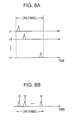
- FIGs. 6A and 6B are diagrams illustrating optical signals that are output from the dispersion medium 25.
- the multi-channel optical signal S IN includes a plurality of optical signals having different optical frequencies v1 to vn.
- the optical signals ⁇ 1 to vn are output from the dispersion medium 25 at different timings.
- the optical signals ⁇ 1 to vn are arranged at regular frequency intervals
- the optical signals ⁇ 1 to vn that are output from the dispersion medium 25 are arranged at regular intervals in the time area.
- each of the optical signals v1 to vn is transformed into a pulse signal by the above-described pulse compression.
- the pulse signals that are generated from the optical signals v1 to vn may be respectively referred to as optical signals t1 to tn.
- a channel that is used to accommodate each of the optical signals t1 to tn may be referred to as a time slot TS.
- a chromatic dispersion amount of the dispersion medium 25 is decided so that the optical signals t1 to tn that are output from the dispersion medium 25 satisfy the following conditions. It is assumed that " ⁇ 1" that corresponds to the optical signal t1 is the minimum frequency of the multi-channel optical signal S IN . In addition, it is assumed that "vn" that corresponds to the optical signal tn is the maximum frequency of the multi-channel optical signal S IN .
- FIG. 6B illustrates optical signals that are output from the dispersion medium 25.
- the optical signals t1 to tn are output from the dispersion medium 25, the optical signals t1 to tn are arranged at approximately regular intervals in the time area. That is, the TDM optical signal in which the optical signals t1 to tn are multiplexed in the time area is output from the dispersion medium 25.
- the modulator 24 and the dispersion medium 25 transform the multi-channel optical signal S IN into the TDM optical signal. That is, the modulator 24 and the dispersion medium 25 transform the frequency area multiplexing optical signal into the time area multiplexing optical signal.
- the modulator 24 and the dispersion medium 25 are examples of optical inverse Fourier transform units.
- the modulator 24 performs both of the phase modulation and the intensity modulation, but the embodiment is not limited to such a configuration.
- the modulator 24 may not perform the intensity modulation on the input optical signal.
- the optical switch 26 drops an optical signal that exists in a time slot to which a pulse signal has been applied, from the TDM optical signal that has been output from the dispersion medium 25.
- the optical switch 26 drops the optical signal t2 from the TDM optical signal by the gate processing in the time area.
- the optical signal t2 that has been dropped from the TDM optical signal is guided to the dispersion medium 29.
- the TDM optical signal from which the optical signal t2 has been dropped is guided to the dispersion medium 27.
- the dispersion medium 27 has a characteristic by which chromatic dispersion by the dispersion medium 25 is compensated. That is, when chromatic dispersion of the dispersion medium 25 is " ⁇ ", chromatic dispersion of the dispersion medium 27 is "- ⁇ ".
- the modulator 28 performs the inverse operation of the modulation operation by the modulator 24. That is, when the modulator 24 applies ⁇ (t) to an optical signal, the modulator 28 applies - ⁇ (t) to an optical signal.
- the TDM optical signal that has been output from the optical switch 26 is transformed into a frequency area optical signal by the dispersion medium 27 and the modulator 28. That is, the dispersion medium 27 and the modulator 28 operate as optical Fourier transform units each of which performs optical Fourier transform on the TDM optical signal.
- the frequency area optical signal that has been obtained by the dispersion medium 27 and the modulator 28 is guided to a through port as a multi-channel optical signal S THRU .
- the multi-channel optical signal S THRU that has been output through the through port is guided, for example, to the optical add device 3 in the OADM 1 illustrated in FIG. 1 .
- the dispersion medium 29 has a characteristic by which the chromatic dispersion by the dispersion medium 25 is compensated.
- the modulator 30 performs the inverse operation of the modulation operation by the modulator 24. That is, the dispersion medium 29 and the modulator 30 operate as optical Fourier transform units each of which performs optical Fourier transform on an optical signal that is dropped from the TDM optical signal.
- the drop optical signal that has been obtained by the dispersion medium 29 and the modulator 30 is output as a drop optical signal S DROP .
- the optical splitter 31 branches the drop optical signal S DROP that has been output from the modulator 30 and guides the drop optical signals S DROP to a drop port and the control unit 32.
- the drop optical signal S DROP that has been output through the drop port is guided, for example, to the client device.
- the control unit 32 monitors the strength or power of the drop optical signal S DROP . In addition, the control unit 32 generates a control signal that is used to maximize the strength or power of the drop optical signal S DROP . The control signal is used to control timing of a pulse signal that is applied from the pulse generator 23 to the optical switch 26. The control unit 32 may monitor the frequency of the drop optical signal S DROP . In this case, the control unit 32 may determine whether or not an optical signal having a desired frequency is dropped from the TDM optical signal appropriately.
- the control unit 32 may be obtained by a processor system that includes a processor and a memory. In addition, the control unit 32 may be obtained by a hardware circuit. In addition, the control unit 32 may be obtained by a combination of software and hardware.
- FIG. 8 illustrates a first example of the optical switch 26.
- the optical switch 26 executes the gate processing in the time area using an optical pulse signal.
- the pulse generator 23 generates an optical pulse signal that is synchronized with the clock signal and applies the generated optical pulse signal to the optical switch 26.
- the optical switch 26 includes a polarization controller 41, a variable delay element 42, an optical multiplexer 43, a nonlinear optical medium 44, and a polarization beam splitter (PBS) 45.
- a TDM optical signal that has been output from the dispersion medium 25 is guided to the polarization controller 41.
- the optical pulse signal that has been generated by the pulse generator 23 is guided to the variable delay element 42.
- the polarization controller 41 controls an input optical signal so that the input optical signal becomes linear polarization that has been specified beforehand.
- the variable delay element 42 delays an input optical pulse signal in accordance with the control signal that has been generated by the control unit 32.
- the variable delay element 42 is obtained, for example, by an optical device the light path length of which is changed depending on the arrangement of a plurality of mirrors. In this case, the arrangement of the mirrors is controlled by the control signal.
- the variable delay element 42 may be obtained by an optical device the light path length of which is changed depending on the temperature of the optical device. In this case, the temperature of the optical device is controlled by the control signal.
- the optical multiplexer 43 multiplexes the optical signal the polarization of which has been controlled by the polarization controller 41 and the optical pulse signal that has been delayed by the variable delay element 42, and guides the multiplexed signals to the nonlinear optical medium 44.
- the nonlinear optical medium 44 is obtained, for example, by a nonlinear optical fiber that provides a nonlinear optical effect (here, Kerr effect).
- the angle of the polarization of the input optical signal is controlled depending on the strength of control light in the nonlinear optical medium 44.
- the optical pulse signal that has been generated by the pulse generator 23 is used as the control light that is used to control the polarization of the input optical signal.
- the pulse of an optical pulse signal may be referred to as a control pulse.
- the PBS 45 includes a first polarization axis and a second polarization axis that are perpendicular to each other.
- an optical component that has been extracted by the first polarization axis is guided to a dispersion medium 27 as an output optical signal 1.
- an optical component that has been extracted by the second polarization axis is guided to a dispersion medium 29 as an output optical signal 2.
- FIGs. 9A and 9B are diagrams illustrating operations of the optical switch 26 illustrated in FIG. 8 .
- the first polarization axis of the PBS 45 is adjusted to 45 degrees.
- the second polarization axis of the PBS 45 is adjusted at an angle that is perpendicular to the first polarization axis.
- the polarization controller 41 controls the polarization of an input optical signal (that is, TDM optical signal) so that the polarization is approximately matched with the first polarization axis of the PBS 45.
- an input optical signal that is, TDM optical signal
- the polarization of the input optical signal is not changed in the nonlinear optical medium 44.
- the polarization of an optical signal that is output from the nonlinear optical medium 44 corresponds to the state illustrated in FIG. 9A .
- the optical signal that has been output from the nonlinear optical medium 44 is extracted by the first polarization axis and guided to the dispersion medium 27.
- the dispersion medium 27 For example, in the example illustrated in FIG.
- a control pulse does not exist in the time slots TS1, and TS3 to TSn.
- the optical signals t1, and t3 to tn are not dropped from the TDM optical signal and are guided to the dispersion medium 27.
- the polarization of the input optical signal is changed in the nonlinear optical medium 44.
- the strength of the control pulse is adjusted so that the polarization of the input optical signal is rotated by about 90 degrees in the nonlinear optical medium 44. Therefore, when a control pulse exists, the polarization of an optical signal that has been output from the nonlinear optical medium 44 corresponds to the state illustrated in FIG. 9B .
- the optical signal that has been output from the nonlinear optical medium 44 is extracted by the second polarization axis and is guided to the dispersion medium 29.
- a control pulse exists in the time slot TS2. In this case, the optical signal t2 is dropped from the TDM optical signal and guided to the dispersion medium 29.
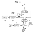
- FIG. 10 is a diagram illustrating a second example of the optical switch 26.
- the optical switch 26 executes the gate processing in the time area using an optical pulse signal.
- the pulse generator 23 generates an optical pulse signal.
- the optical switch 26 executes the gate processing in the time area using a nonlinear optical loop mirror (NOLM).
- NOLM nonlinear optical loop mirror
- the optical switch 26 of the second example includes an optical circulator 51, an optical multiplexer 52, a nonlinear optical medium 53, a variable delay element 54, and an optical multiplexer 55.
- the TDM optical signal that has been output from the dispersion medium 25 is guided to the optical circulator 51.
- the optical pulse signal that has been generated by the pulse generator 23 is guided to the variable delay element 54.
- the optical circulator 51 guides the input optical signal to the optical multiplexer 52.
- the optical circulator 51 guides the optical signal that has been output from the optical multiplexer 52, to an output port P2.
- the optical multiplexer 52 branches the input optical signal that has been guided from the optical circulator 51 and propagates the input optical signals to the nonlinear optical medium 53 bidirectionally.
- the nonlinear optical medium 53 is formed in a loop shape.
- the input optical signals that has been branched by the optical multiplexer 52 are propagated to the nonlinear optical medium 53 bidirectionally (that is, in the clockwise direction and counter-clockwise direction).
- the nonlinear optical medium 53 is obtained, for example, by a nonlinear optical fiber that provides a nonlinear optical effect.
- the variable delay element 54 causes a control pulse to be delayed in accordance with the control signal that has been generated by the control unit 32.
- the variable delay element 54 is substantially the same as the variable delay element 42 illustrated in FIG. 8 , so that the description is omitted herein.
- the optical multiplexer 55 inputs the control pulse that has been delayed by the variable delay element 54, to the nonlinear optical medium 53. At this time, the control pulse is input to the nonlinear optical medium 53 so as to be propagated to the nonlinear optical medium 53 in a certain direction (for example, clockwise direction).
- the input optical signal that has been propagated to the nonlinear optical medium 53 in the clockwise direction and the input optical signal that has been propagated to the nonlinear optical medium 53 in the counter-clockwise direction are multiplexed with each other.
- the multiplexed optical signal is guided to the output port P1.
- the optical signal that has been output though the output port P1 (output optical signal 1) is guided to the dispersion medium 27.
- an input optical signal that is propagated in the same direction as the control pulse receives the nonlinear optical effect.
- an input optical signal and the input optical signal that has received the nonlinear optical effect in the nonlinear optical medium 53 are multiplexed with each other.
- the multiplexed optical signals are guided to the output port P2 through the optical circulator 51.
- the optical signal has been output though the output port P2 (output optical signal 2) is guided to the dispersion medium 29.
- the optical switch 26 may further include a polarization controller 56 that controls the polarization of the input optical signal.
- the polarization controller 56 controls the polarization of the input optical signal so that an extinction ratio between a case in which a control pulse exists and a case in which a control pulse does not exist is improved.
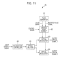
- FIG. 11 is a diagram illustrating a third example of the optical switch 26.
- the optical switch 26 executes the gate processing in the time area using an electrical pulse signal.
- the pulse generator 23 generates an electrical pulse signal.
- the pulse generator 23 generates a pulse signal and an inverted pulse signal. In the pulse signal and the inverted pulse signal, the logics are inverted to each other.
- the optical switch 26 includes an optical splitter 61, a variable delay element 62, and optical modulators 63 and 64.
- the optical splitter 61 branches an input optical signal and guides the input optical signals to the optical modulators 63 and 64.
- the variable delay element 62 causes a pulse signal and an inverted pulse signal to be delayed in accordance with the control signal that has been generated by the control unit 32.
- the optical modulators 63 and 64 operate as strength modulators. That is, the optical modulator 63 controls the strength of the input optical signal in accordance with the pulse signal. Similarly, the optical modulator 64 controls the strength of the input optical signal in accordance with the inverted pulse signal.
- the optical modulator 63 when a control pulse does not exist (when a control pulse of the inverted pulse signal exists), the optical modulator 63 causes the input optical signal to pass through the optical modulator 63, and the optical modulator 64 cuts off the input optical signal.
- the optical modulator 63 cuts off the input optical signal, and the optical modulator 64 causes the input optical signal to pass through the optical modulator 64.
- the gate processing that is similar to that by the configuration illustrated in FIG. 8 or 10 may be executed.
- the optical switch 26 may further include a polarization controller 65 that controls the polarization of the input optical signal.
- the polarization controller 65 controls the polarization of the input optical signal so that an extinction ratio between a case in which a control pulse exists and a case in which a control pulse does not exist is improved.
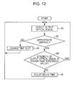
- FIG. 12 is a flowchart illustrating the drop processing in the optical drop device illustrated in FIG. 3 .
- the processing is executed by the control unit 32.
- the processing is executed, for example, on a regular basis.
- control unit 32 detects an optical signal that has been output from the modulator 30 (optical signal S DROP ). At this time, the control unit 32 monitors the optical frequency and the strength of the output optical signal. In S2, the control unit 32 determines whether or not the optical frequency of the output optical signal is matched with the optical frequency of a specified drop channel.
- control unit 32 determines that the optical frequency of the output optical signal is not matched with the optical frequency of the specified drop channel, the control unit 32 changes a time slot to which a control pulse is applied in the optical switch 26, in S3.
- the processing of S3 is achieved by generating a control signal that is used to control a delay time of the variable delay element (variable delay elements 42, 54, and 62 in FIGs. 8 , 10 , and 11 , respectively).
- the control unit 32 determines that the optical frequency of the output optical signal is matched with the optical frequency of the specified drop channel, the processing of S3 is skipped.
- control unit 32 compares the strength of the output optical signal with a certain threshold value. In addition, when the strength of the output optical signal is a certain threshold value or less, the control unit 32 generates a control signal that is used to control a delay time of the variable delay element. A change amount of the delay time in S4 is sufficiently small as compared with that in S3. On the other hand, when the strength of the output optical signal is more than the certain threshold value, the control unit 32 does not change and maintains the control signal.
- the delay time of a pulse signal is controlled so that the strength of the drop optical signal becomes higher than the threshold value, but the embodiment is not limited to such a method. That is, for example, the control unit 32 may control the delay time of the pulse signal so that the strength of the dropped optical signal is maximized.
- FIG. 13 is a diagram illustrating a configuration of a first example of the optical add device.
- an optical add device 3A of the first example includes an optical inverse Fourier transform unit 71, an optical inverse Fourier transform unit 72, an optical multiplexer 73, and an optical Fourier transform unit 74.
- the four channels ⁇ 1 to v4 are multiplexed in a multi-channel optical signal S.
- a multi-channel optical signal S THRU is input.
- the multi-channel optical signal S THRU is output, for example, from the optical drop device 2 in the OADM 1 illustrated in FIG. 1 .
- the multi-channel optical signal S THRU includes the optical signals v1, v2, and v4.
- the optical signals v1, v2, and ⁇ 4 are multiplexed in the frequency area.
- the optical inverse Fourier transform unit 71 transforms the multi-channel optical signal S THRU into a TDM optical signal.
- the TDM optical signal transmission of the optical signals t1 to t4 is performed using the time slots TS1 to TS4.
- the time slots TS1 to TS4 respectively corresponds to the frequency channels ⁇ 1 to ⁇ 4.
- the optical inverse Fourier transform unit 71 generates the TDM optical signal that includes the optical signals t1, t2, and t4.
- the optical signals t1, t2, and t4 are multiplexed in the time area.
- an optical signal is not accommodated.
- an optical signal S ADD is input.
- the optical signal S ADD is transmitted, for example, from the client device.
- the optical frequency of the optical signal S ADD is "v3".
- the optical inverse Fourier transform unit 72 transforms the optical signal S ADD into a time area optical signal (optical signal t3 in FIG. 13 ).
- the optical multiplexer 73 multiplexes the TDM optical signal that has been generated by the optical inverse Fourier transform unit 71 and the time area optical signal that has been generated by the optical inverse Fourier transform unit 72. At this time, the TDM optical signal and the optical signal t3 are multiplexed with each other so that the optical signal t3 is accommodated in the time slot TS3.
- the optical Fourier transform unit 74 transforms the optical signals t1 to t4 that have been output from the optical multiplexer 73, into frequency area optical signals. That is, the optical Fourier transform unit 74 executes transformation processing that corresponds to the optical inverse Fourier transform unit 71 or 72. As a result, the optical Fourier transform unit 74 generates a multi-channel optical signal S OUT that includes the optical signals v1 to v4. The optical signals v1 to ⁇ 4 are multiplexed with each other in the frequency area.
- the optical add device 3A transforms the multi-channel optical signal in the frequency area into the TDM optical signal in the time area, and adds an optical signal to the TDM optical signal in the time area.
- suppression of light loss is expected as compared with the configuration in which an optical signal is added to the multi-channel optical signal in the frequency area.
- FIG. 14 illustrates a configuration of a second example of the optical add device.
- an optical drop device 3B of the second example includes an optical splitter 81, a clock extractor 82, a modulator 83, a dispersion medium 84, a modulator 85, a dispersion medium 86, a variable delay element 87, an optical multiplexer 88, a dispersion medium 89, a modulator 90, an optical splitter 91, an optical filter 92, and a control unit 93.
- a multi-channel optical signal S THRU includes a plurality of optical signals having different optical frequencies.
- it is desirable that dispersion that is applied to the multi-channel optical signal S THRU is sufficiently compensated.
- the configurations and operations of the optical splitter 81, the clock extractor 82, the modulator 83, and the dispersion medium 84 are substantially the same as the optical splitter 21, the clock extractor 22, the modulator 24, and the dispersion medium 25 of the optical drop device illustrated in FIG. 3 .
- the modulator 83 and the dispersion medium 84 operate as optical inverse Fourier transform units for the multi-channel optical signal S THRU . That is, the multi-channel optical signal S THRU is transformed into a TDM optical signal by the modulator 83 and the dispersion medium 84.
- optical splitter 81 The configurations and operations of the optical splitter 81, the clock extractor 82, the modulator 85, and the dispersion medium 86 are also substantially the same as the optical splitter 21, the clock extractor 22, the modulator 24, and the dispersion medium 25, which are illustrated in FIG. 3 .
- the optical signal S ADD is transformed into a time area optical signal by the modulator 85and the dispersion medium 86.
- the variable delay element 87 causes an optical signal that has been output from the dispersion medium 86 to be delayed, in accordance with a control signal that has been generated by the control unit 93.
- the configuration and operation of the variable delay element 87 is, for example, similar to the variable delay element 42 illustrated in FIG. 8 .
- the optical multiplexer 88 multiplexes an optical signal that has been output from the dispersion medium 84 and an optical signal that has been output from the variable delay element 87.
- the time area optical signal that corresponds to the optical signal S ADD is added to the TDM optical signal that corresponds to the multi-channel optical signal S THRU .
- the configurations and operations of the dispersion medium 89 and the modulator 90 are substantially the same as the dispersion medium 27 and the modulator 28 of the optical drop device illustrated in FIG. 3 .
- the dispersion medium 89 and the modulator 90 transform the TDM optical signal that has been output from the optical multiplexer 88 into a frequency area optical signal.
- the frequency area optical signal includes the optical signal S ADD and the optical signals of the multi-channel optical signal S THRU .
- the frequency area optical signal is transmitted to the network as a multi-channel optical signal S OUT .
- the optical splitter 91 branches the multi-channel optical signal S OUT and guides the multi-channel optical signal S OUT to the optical filter 92.
- the optical filter 92 extracts the frequency component of the optical signal S ADD from the multi-channel optical signal S OUT . It is assumed that the frequency component of the optical signal S ADD is known component.
- the optical filter 92 is, for example, a tunable frequency filter.
- the control unit 93 monitors the strength of the frequency component that has been extracted by the optical filter 92. That is, the control unit 93 monitors the strength of the optical signal S ADD that is included in the multi-channel optical signal S OUT . In addition, the control unit 93 generates a control signal that is used to maximize the strength of the optical signal S ADD . The control signal is used to control a delay amount of the variable delay element 87.
- the control unit 93 may be obtained by a processor system that includes a processor and a memory. In addition, the control unit 93 may be obtained by a hardware circuit. In addition, the control unit 93 may be obtained by a combination of software and hardware.
- the optical add device 3B adds the optical signal S ADD to the multi-channel optical signal S THRU illustrated in FIG. 13 .
- the optical signals v1, v2, and v4 that are included in the multi-channel optical signal S THRU are transformed into the optical signals t1, t2, and t4 that are accommodated in the time slots TS1, TS2, and TS4 by the modulator 83 and the dispersion medium 84.
- the multi-channel optical signal S THRU does not include the optical signal v3, so that the time slot TS3 of the TDM optical signal is free.
- the optical signal S ADD (that is, the optical signal v3) is transformed into the optical signal t3 by the modulator 85 and the dispersion medium 86.
- the control unit 93 controls the delay amount of the variable delay element 87 so that the optical signal t3 is added to the time slot TS3 of the TDM optical signal appropriately.
- the v3 component that is obtained by the optical Fourier transform unit that is, the dispersion medium 93 and the modulator 90
- the control unit 93 may add an optical signal to a specified time slot appropriately by monitoring the v3 component.
- FIG. 15 illustrates a configuration of a third example of the optical add device.
- an optical add device 3C of the third example includes a continuous wave (CW) light source 101, an optical multiplexer 102, a CW light source 103, an optical multiplexer 104, an optical multiplexer 105, a nonlinear optical medium 106, an optical filter 107, an optical splitter 108, an optical filter 109, and a control unit 110.
- CW continuous wave
- a multi-channel optical signal S THRU by a multi-channel optical signal S THRU , transmission of optical signals may be performed using the channels v1 to vn.
- the multi-channel optical signal S THRU does not include an optical signal having an optical frequency v TA .
- the optical frequency of the optical signal S ADD that is to be added to the multi-channel optical signal S THRU is " ⁇ AS ".
- the optical frequency ⁇ AS is located outside the frequency band of the multi-channel optical signal S THRU .
- the CW light source 101 generates CW light of an optical frequency ⁇ T0 .
- the optical frequency ⁇ T0 is located outside the frequency band of the multi-channel optical signal S THRU .
- the optical multiplexer 102 multiplexes the CW light that is generated by the CW light source 101 and the multi-channel optical signal S THRU .
- the CW light source 103 generates CW light of an optical frequency ⁇ A0 .
- the optical frequency ⁇ A0 is also located outside the frequency band of the multi-channel optical signal S THRU .
- “ ⁇ T0" and “ ⁇ A0 " are different from each other.
- the optical multiplexer 104 multiplexes the optical signal S ADD and the CW light that is generated by the CW light source 103.
- the optical multiplexer 105 multiplexes the optical signal that has been output from the optical multiplexer 102 and the optical signal that has been output from the optical multiplexer 104. That is, the multi-channel optical signal S THRU , the optical signal S ADD , the CW light of the optical frequency ⁇ T0 , the CW light of the optical frequency ⁇ A0 are multiplexed with each other. In addition, the output optical signal of the optical multiplexer 105 is propagated through the nonlinear optical medium 106. It is assumed that " ⁇ T0 " and " ⁇ A0 " are controlled so that the following condition (1) is satisfied.
- the nonlinear optical medium 106 cross-phase modulation is performed on the CW light ⁇ T0 due to beat between the optical signal S ADD and the CW light ⁇ A0 , so that an optical signal that corresponds to the optical signal S ADD appears in the optical frequency v TA . That is, the optical signal S ADD that includes the optical frequency ⁇ TA is obtained.
- the optical filter 107 causes the frequency band ( ⁇ 1 to vn) of the multi-channel optical signal to pass through the optical filter 107.
- the optical signal S ADD of the optical frequency ⁇ AS , the CW light ⁇ A0 , and the CW light ⁇ T0 are reduced by the optical filter 107.
- the optical signal from which an unnecessary frequency component has been reduced by the optical filter 107 is output to the network as the multi-channel optical signal S OUT .
- the optical splitter 108 branches the multi-channel optical signal S OUT and guides the multi-channel optical signal S OUT to the optical filter 109.
- the optical filter 109 extracts the v TA component from the multi-channel optical signal S OUT .
- " ⁇ TA " is an optical frequency to which an optical signal has been added.
- the control unit 110 generates a control signal that is used to control at least one of " ⁇ T0 " and " ⁇ A0 " in order to maximize the ⁇ TA component.
- the control signal is applied to the CW light source 101 and/or the CW light source 103.
- the optical signal S ADD is added to a free time slot of the multi-channel optical signal S THRU appropriately.
- FIG. 17 illustrates a configuration of a fourth example of the optical add device.
- An optical drop device 3D of the fourth example is a modification of the third example illustrated in FIG. 15 . That is, in the third example, the CW light ⁇ T0 and the CW light ⁇ A0 are respectively generated from the CW light sources 101 and 103. On contrast, in the fourth example, CW light ⁇ T0 is generated from a multi-channel optical signal S THRU . In addition, CW light ⁇ A0 is generated from an optical signal S ADD ,
- An optical splitter 111 branches the multi-channel optical signal S THRU and guides the multi-channel optical signals S THRU to an optical multiplexer 114 and an optical phase lock loop (PLL) circuit 112.
- the optical PLL circuit 112 generates CW light from an optical signal having a frequency ⁇ T1 that is included in the multi-channel optical signal S THRU .
- the frequency of the CW light is also " ⁇ T1 ".
- a frequency shifter 113 shifts the frequency of the CW light that has been generated by the optical PLL circuit 112 from " ⁇ T1 " to " ⁇ T0 ".
- the optical multiplexer 114 multiplexes the multi-channel optical signal S THRU and the CW light ⁇ T0 that has been obtained by the frequency shifter 113.
- An optical splitter 115 branches an optical signal S ADD and guides the add optical signals S ADD to an optical multiplexer 118 and an optical PLL circuit 116.
- the frequency of the add optical signal S ADD is " ⁇ AS ".
- the optical PLL circuit 116 generates CW light from the optical signal S ADD .
- the frequency of the CW light is also " ⁇ AS ".
- a frequency shifter 117 shifts the frequency of the CW light that has been generated by the optical PLL circuit 116 from " ⁇ AS " to " ⁇ A0 ".
- the optical multiplexer 118 multiplexes the optical signal S ADD and the CW light ⁇ A0 that has been obtained by the frequency shifter 117.
- An optical multiplexer 119 multiplexes the optical signal that has been output from the optical multiplexer 114 and the optical signal that has been output from the optical multiplexer 118. That is, the multi-channel optical signal S THRU , the optical signal S ADD , the CW light ⁇ T0 , and the CW light ⁇ A0 are multiplexed with each other. In addition, the optical signal that has been output from the optical multiplexer 119 is guided to the nonlinear optical medium 106.
- the configurations and operations of the nonlinear optical medium 106, the optical filter 107, the optical splitter 108, the optical filter 109, and the control unit 110 are substantially the same as those of the third example and the fourth example, and the description is omitted herein.
- the configurations that are used to generate CW light are different from each other, but an optical signal is added to a multi-channel optical signal by the substantially same optical operations.
- the CW light sources 101 and 103 are examples of CW light generators.
- the optical PLL circuits 112 and 116, and the frequency shifters 113 and 117 are examples of CW light generators.
Landscapes
- Engineering & Computer Science (AREA)
- Computer Networks & Wireless Communication (AREA)
- Signal Processing (AREA)
- Optical Communication System (AREA)
- Optical Modulation, Optical Deflection, Nonlinear Optics, Optical Demodulation, Optical Logic Elements (AREA)
Applications Claiming Priority (1)
| Application Number | Priority Date | Filing Date | Title |
|---|---|---|---|
| JP2013240567A JP2015103831A (ja) | 2013-11-21 | 2013-11-21 | 光分岐装置および光挿入装置 |
Publications (2)
| Publication Number | Publication Date |
|---|---|
| EP2876829A1 true EP2876829A1 (fr) | 2015-05-27 |
| EP2876829B1 EP2876829B1 (fr) | 2016-06-29 |
Family
ID=51897204
Family Applications (1)
| Application Number | Title | Priority Date | Filing Date |
|---|---|---|---|
| EP14193427.3A Not-in-force EP2876829B1 (fr) | 2013-11-21 | 2014-11-17 | Dispositif et procédé d'extraction optique et dispositif optique d'insertion |
Country Status (3)
| Country | Link |
|---|---|
| US (1) | US9450699B2 (fr) |
| EP (1) | EP2876829B1 (fr) |
| JP (1) | JP2015103831A (fr) |
Families Citing this family (1)
| Publication number | Priority date | Publication date | Assignee | Title |
|---|---|---|---|---|
| JP6988296B2 (ja) * | 2017-09-14 | 2022-01-05 | 富士通株式会社 | 伝送装置及び信号監視方法 |
Citations (3)
| Publication number | Priority date | Publication date | Assignee | Title |
|---|---|---|---|---|
| WO1995010870A1 (fr) * | 1993-10-11 | 1995-04-20 | British Telecommunications Public Limited Company | Generateur de sequence d'impulsions optiques |
| EP1185007A2 (fr) * | 2000-09-01 | 2002-03-06 | Fujitsu Limited | Procédé, dispositif et système de traitement de signaux optiques |
| JP2012119925A (ja) | 2010-11-30 | 2012-06-21 | Nippon Telegr & Teleph Corp <Ntt> | Roadm装置及び光アド・ドロップ方法 |
Family Cites Families (4)
| Publication number | Priority date | Publication date | Assignee | Title |
|---|---|---|---|---|
| JP2991131B2 (ja) * | 1996-10-07 | 1999-12-20 | 日本電気株式会社 | 信号光チャネル数計数器とこれを用いた光増幅装置 |
| US6388782B1 (en) * | 1998-06-01 | 2002-05-14 | Sarnoff Corporation | Multi-wavelength dense wavelength division multiplexed optical switching systems |
| JP4030441B2 (ja) * | 2003-02-26 | 2008-01-09 | 富士通株式会社 | 光クロスコネクト装置 |
| JP2013005216A (ja) * | 2011-06-16 | 2013-01-07 | Nec Corp | 光伝送システム及び光伝送方法 |
-
2013
- 2013-11-21 JP JP2013240567A patent/JP2015103831A/ja not_active Ceased
-
2014
- 2014-11-11 US US14/538,175 patent/US9450699B2/en not_active Expired - Fee Related
- 2014-11-17 EP EP14193427.3A patent/EP2876829B1/fr not_active Not-in-force
Patent Citations (3)
| Publication number | Priority date | Publication date | Assignee | Title |
|---|---|---|---|---|
| WO1995010870A1 (fr) * | 1993-10-11 | 1995-04-20 | British Telecommunications Public Limited Company | Generateur de sequence d'impulsions optiques |
| EP1185007A2 (fr) * | 2000-09-01 | 2002-03-06 | Fujitsu Limited | Procédé, dispositif et système de traitement de signaux optiques |
| JP2012119925A (ja) | 2010-11-30 | 2012-06-21 | Nippon Telegr & Teleph Corp <Ntt> | Roadm装置及び光アド・ドロップ方法 |
Non-Patent Citations (2)
| Title |
|---|
| HIROOKA T ET AL: "All-optical 40 GHz Time-domain Fourier Transformation Using XPM with a Dark Parabolic Pulse", OPTICAL FIBER COMMUNICATION/NATIONAL FIBER OPTIC ENGINEERS CONFERENCE, 2008. OFC/NFOEC 2008. CONFERENCE ON, IEEE, PISCATAWAY, NJ, USA, 24 February 2008 (2008-02-24), pages 1 - 3, XP031391569, ISBN: 978-1-55752-856-8 * |
| MISHRA A K ET AL: "Comb generator for 100 Gbit/s OFDM and low-loss comb-line combiner using the optical inverse fourier transform (IFFT)", TRANSPARENT OPTICAL NETWORKS (ICTON), 2011 13TH INTERNATIONAL CONFERENCE ON, IEEE, 26 June 2011 (2011-06-26), pages 1 - 5, XP031911911, ISBN: 978-1-4577-0881-7, DOI: 10.1109/ICTON.2011.5971034 * |
Also Published As
| Publication number | Publication date |
|---|---|
| JP2015103831A (ja) | 2015-06-04 |
| US9450699B2 (en) | 2016-09-20 |
| US20150139644A1 (en) | 2015-05-21 |
| EP2876829B1 (fr) | 2016-06-29 |
Similar Documents
| Publication | Publication Date | Title |
|---|---|---|
| EP0729057B1 (fr) | Source de lumière blanche cohérente et dispositifs optiques avec la même | |
| US20170250775A1 (en) | Optical multiplexing device and optical multiplexing network system | |
| EP1653652B1 (fr) | Récupération optique d'horloge et dispositif correspondant | |
| US8705980B2 (en) | Optical modulation device and optical modulation method | |
| JP2007240389A (ja) | 光波形測定装置および光波形測定方法 | |
| JP5786565B2 (ja) | 光多重装置および光ネットワークシステム | |
| JP4733745B2 (ja) | 光信号処理装置 | |
| EP0924552A2 (fr) | Circuit diviseur de fréquence opto-électronique et son procédé d'opération | |
| JP4444689B2 (ja) | 光通信用光装置 | |
| US9746699B2 (en) | Optical frequency shifter, single sideband modulator, and light insertion and branch apparatus | |
| JP5107863B2 (ja) | 光直交周波数分割多重伝送用回路 | |
| US9148228B2 (en) | Optical signal transmitting device, optical signal transmitting method, frequency fluctuation suppressing device and frequency fluctuation suppressing system | |
| US20030231885A1 (en) | Optical multiplexing communication system using ultra high speed signal transmission | |
| EP2876829B1 (fr) | Dispositif et procédé d'extraction optique et dispositif optique d'insertion | |
| EP1458127B1 (fr) | Procédé et dispositif de fourniture d'une source optique à pluralité de longueurs d'ondes | |
| CN102055527A (zh) | 一种产生多载波光的方法 | |
| US6741810B2 (en) | Signal demultiplexing device and signal routing device in high speed transmission system | |
| US8537452B2 (en) | System and method for generating optical radiation of controllable spectral content | |
| JP4252470B2 (ja) | Otdm/wdm伝送方法及び装置 | |
| JP2018180406A (ja) | 波長変換装置、制御光生成装置、波長変換方法、および制御光生成方法 | |
| KR0153909B1 (ko) | 주파수 이동기를 이용한 의사등간격 다채널 주파수 발생장치 | |
| EP2725725A1 (fr) | Système de transmission optique et procédé de commande | |
| EP1571765B1 (fr) | Element optique de synchronisation | |
| Oxenløwe et al. | Energy-efficient optical signal processing using optical time lenses |
Legal Events
| Date | Code | Title | Description |
|---|---|---|---|
| PUAI | Public reference made under article 153(3) epc to a published international application that has entered the european phase |
Free format text: ORIGINAL CODE: 0009012 |
|
| 17P | Request for examination filed |
Effective date: 20141117 |
|
| AK | Designated contracting states |
Kind code of ref document: A1 Designated state(s): AL AT BE BG CH CY CZ DE DK EE ES FI FR GB GR HR HU IE IS IT LI LT LU LV MC MK MT NL NO PL PT RO RS SE SI SK SM TR |
|
| AX | Request for extension of the european patent |
Extension state: BA ME |
|
| R17P | Request for examination filed (corrected) |
Effective date: 20150527 |
|
| RBV | Designated contracting states (corrected) |
Designated state(s): AL AT BE BG CH CY CZ DE DK EE ES FI FR GB GR HR HU IE IS IT LI LT LU LV MC MK MT NL NO PL PT RO RS SE SI SK SM TR |
|
| GRAP | Despatch of communication of intention to grant a patent |
Free format text: ORIGINAL CODE: EPIDOSNIGR1 |
|
| RIC1 | Information provided on ipc code assigned before grant |
Ipc: H04J 14/08 20060101ALI20150924BHEP Ipc: H04J 14/02 20060101AFI20150924BHEP Ipc: H04Q 11/00 20060101ALI20150924BHEP |
|
| INTG | Intention to grant announced |
Effective date: 20151013 |
|
| INTG | Intention to grant announced |
Effective date: 20151209 |
|
| GRAS | Grant fee paid |
Free format text: ORIGINAL CODE: EPIDOSNIGR3 |
|
| GRAA | (expected) grant |
Free format text: ORIGINAL CODE: 0009210 |
|
| AK | Designated contracting states |
Kind code of ref document: B1 Designated state(s): AL AT BE BG CH CY CZ DE DK EE ES FI FR GB GR HR HU IE IS IT LI LT LU LV MC MK MT NL NO PL PT RO RS SE SI SK SM TR |
|
| REG | Reference to a national code |
Ref country code: GB Ref legal event code: FG4D |
|
| REG | Reference to a national code |
Ref country code: CH Ref legal event code: EP |
|
| REG | Reference to a national code |
Ref country code: AT Ref legal event code: REF Ref document number: 809829 Country of ref document: AT Kind code of ref document: T Effective date: 20160715 |
|
| REG | Reference to a national code |
Ref country code: IE Ref legal event code: FG4D |
|
| REG | Reference to a national code |
Ref country code: DE Ref legal event code: R096 Ref document number: 602014002490 Country of ref document: DE |
|
| REG | Reference to a national code |
Ref country code: FR Ref legal event code: PLFP Year of fee payment: 3 |
|
| REG | Reference to a national code |
Ref country code: LT Ref legal event code: MG4D |
|
| PG25 | Lapsed in a contracting state [announced via postgrant information from national office to epo] |
Ref country code: LT Free format text: LAPSE BECAUSE OF FAILURE TO SUBMIT A TRANSLATION OF THE DESCRIPTION OR TO PAY THE FEE WITHIN THE PRESCRIBED TIME-LIMIT Effective date: 20160629 Ref country code: NO Free format text: LAPSE BECAUSE OF FAILURE TO SUBMIT A TRANSLATION OF THE DESCRIPTION OR TO PAY THE FEE WITHIN THE PRESCRIBED TIME-LIMIT Effective date: 20160929 Ref country code: FI Free format text: LAPSE BECAUSE OF FAILURE TO SUBMIT A TRANSLATION OF THE DESCRIPTION OR TO PAY THE FEE WITHIN THE PRESCRIBED TIME-LIMIT Effective date: 20160629 |
|
| REG | Reference to a national code |
Ref country code: NL Ref legal event code: MP Effective date: 20160629 |
|
| PG25 | Lapsed in a contracting state [announced via postgrant information from national office to epo] |
Ref country code: GR Free format text: LAPSE BECAUSE OF FAILURE TO SUBMIT A TRANSLATION OF THE DESCRIPTION OR TO PAY THE FEE WITHIN THE PRESCRIBED TIME-LIMIT Effective date: 20160930 Ref country code: HR Free format text: LAPSE BECAUSE OF FAILURE TO SUBMIT A TRANSLATION OF THE DESCRIPTION OR TO PAY THE FEE WITHIN THE PRESCRIBED TIME-LIMIT Effective date: 20160629 Ref country code: SE Free format text: LAPSE BECAUSE OF FAILURE TO SUBMIT A TRANSLATION OF THE DESCRIPTION OR TO PAY THE FEE WITHIN THE PRESCRIBED TIME-LIMIT Effective date: 20160629 Ref country code: LV Free format text: LAPSE BECAUSE OF FAILURE TO SUBMIT A TRANSLATION OF THE DESCRIPTION OR TO PAY THE FEE WITHIN THE PRESCRIBED TIME-LIMIT Effective date: 20160629 Ref country code: RS Free format text: LAPSE BECAUSE OF FAILURE TO SUBMIT A TRANSLATION OF THE DESCRIPTION OR TO PAY THE FEE WITHIN THE PRESCRIBED TIME-LIMIT Effective date: 20160629 Ref country code: NL Free format text: LAPSE BECAUSE OF FAILURE TO SUBMIT A TRANSLATION OF THE DESCRIPTION OR TO PAY THE FEE WITHIN THE PRESCRIBED TIME-LIMIT Effective date: 20160629 |
|
| REG | Reference to a national code |
Ref country code: AT Ref legal event code: MK05 Ref document number: 809829 Country of ref document: AT Kind code of ref document: T Effective date: 20160629 |
|
| PG25 | Lapsed in a contracting state [announced via postgrant information from national office to epo] |
Ref country code: EE Free format text: LAPSE BECAUSE OF FAILURE TO SUBMIT A TRANSLATION OF THE DESCRIPTION OR TO PAY THE FEE WITHIN THE PRESCRIBED TIME-LIMIT Effective date: 20160629 Ref country code: RO Free format text: LAPSE BECAUSE OF FAILURE TO SUBMIT A TRANSLATION OF THE DESCRIPTION OR TO PAY THE FEE WITHIN THE PRESCRIBED TIME-LIMIT Effective date: 20160629 Ref country code: SK Free format text: LAPSE BECAUSE OF FAILURE TO SUBMIT A TRANSLATION OF THE DESCRIPTION OR TO PAY THE FEE WITHIN THE PRESCRIBED TIME-LIMIT Effective date: 20160629 Ref country code: IT Free format text: LAPSE BECAUSE OF FAILURE TO SUBMIT A TRANSLATION OF THE DESCRIPTION OR TO PAY THE FEE WITHIN THE PRESCRIBED TIME-LIMIT Effective date: 20160629 Ref country code: CZ Free format text: LAPSE BECAUSE OF FAILURE TO SUBMIT A TRANSLATION OF THE DESCRIPTION OR TO PAY THE FEE WITHIN THE PRESCRIBED TIME-LIMIT Effective date: 20160629 Ref country code: IS Free format text: LAPSE BECAUSE OF FAILURE TO SUBMIT A TRANSLATION OF THE DESCRIPTION OR TO PAY THE FEE WITHIN THE PRESCRIBED TIME-LIMIT Effective date: 20161029 |
|
| PG25 | Lapsed in a contracting state [announced via postgrant information from national office to epo] |
Ref country code: PL Free format text: LAPSE BECAUSE OF FAILURE TO SUBMIT A TRANSLATION OF THE DESCRIPTION OR TO PAY THE FEE WITHIN THE PRESCRIBED TIME-LIMIT Effective date: 20160629 Ref country code: BE Free format text: LAPSE BECAUSE OF FAILURE TO SUBMIT A TRANSLATION OF THE DESCRIPTION OR TO PAY THE FEE WITHIN THE PRESCRIBED TIME-LIMIT Effective date: 20160629 Ref country code: AT Free format text: LAPSE BECAUSE OF FAILURE TO SUBMIT A TRANSLATION OF THE DESCRIPTION OR TO PAY THE FEE WITHIN THE PRESCRIBED TIME-LIMIT Effective date: 20160629 Ref country code: PT Free format text: LAPSE BECAUSE OF FAILURE TO SUBMIT A TRANSLATION OF THE DESCRIPTION OR TO PAY THE FEE WITHIN THE PRESCRIBED TIME-LIMIT Effective date: 20161031 Ref country code: SM Free format text: LAPSE BECAUSE OF FAILURE TO SUBMIT A TRANSLATION OF THE DESCRIPTION OR TO PAY THE FEE WITHIN THE PRESCRIBED TIME-LIMIT Effective date: 20160629 Ref country code: ES Free format text: LAPSE BECAUSE OF FAILURE TO SUBMIT A TRANSLATION OF THE DESCRIPTION OR TO PAY THE FEE WITHIN THE PRESCRIBED TIME-LIMIT Effective date: 20160629 |
|
| REG | Reference to a national code |
Ref country code: DE Ref legal event code: R097 Ref document number: 602014002490 Country of ref document: DE |
|
| PG25 | Lapsed in a contracting state [announced via postgrant information from national office to epo] |
Ref country code: DK Free format text: LAPSE BECAUSE OF FAILURE TO SUBMIT A TRANSLATION OF THE DESCRIPTION OR TO PAY THE FEE WITHIN THE PRESCRIBED TIME-LIMIT Effective date: 20160629 |
|
| 26N | No opposition filed |
Effective date: 20170330 |
|
| PLBE | No opposition filed within time limit |
Free format text: ORIGINAL CODE: 0009261 |
|
| STAA | Information on the status of an ep patent application or granted ep patent |
Free format text: STATUS: NO OPPOSITION FILED WITHIN TIME LIMIT |
|
| REG | Reference to a national code |
Ref country code: IE Ref legal event code: MM4A |
|
| PG25 | Lapsed in a contracting state [announced via postgrant information from national office to epo] |
Ref country code: BG Free format text: LAPSE BECAUSE OF FAILURE TO SUBMIT A TRANSLATION OF THE DESCRIPTION OR TO PAY THE FEE WITHIN THE PRESCRIBED TIME-LIMIT Effective date: 20160929 Ref country code: SI Free format text: LAPSE BECAUSE OF FAILURE TO SUBMIT A TRANSLATION OF THE DESCRIPTION OR TO PAY THE FEE WITHIN THE PRESCRIBED TIME-LIMIT Effective date: 20160629 |
|
| PG25 | Lapsed in a contracting state [announced via postgrant information from national office to epo] |
Ref country code: LU Free format text: LAPSE BECAUSE OF NON-PAYMENT OF DUE FEES Effective date: 20161130 |
|
| REG | Reference to a national code |
Ref country code: FR Ref legal event code: PLFP Year of fee payment: 4 |
|
| PG25 | Lapsed in a contracting state [announced via postgrant information from national office to epo] |
Ref country code: IE Free format text: LAPSE BECAUSE OF NON-PAYMENT OF DUE FEES Effective date: 20161117 |
|
| PGFP | Annual fee paid to national office [announced via postgrant information from national office to epo] |
Ref country code: DE Payment date: 20171114 Year of fee payment: 4 Ref country code: FR Payment date: 20171012 Year of fee payment: 4 |
|
| PG25 | Lapsed in a contracting state [announced via postgrant information from national office to epo] |
Ref country code: HU Free format text: LAPSE BECAUSE OF FAILURE TO SUBMIT A TRANSLATION OF THE DESCRIPTION OR TO PAY THE FEE WITHIN THE PRESCRIBED TIME-LIMIT; INVALID AB INITIO Effective date: 20141117 |
|
| PG25 | Lapsed in a contracting state [announced via postgrant information from national office to epo] |
Ref country code: CY Free format text: LAPSE BECAUSE OF FAILURE TO SUBMIT A TRANSLATION OF THE DESCRIPTION OR TO PAY THE FEE WITHIN THE PRESCRIBED TIME-LIMIT Effective date: 20160629 Ref country code: MK Free format text: LAPSE BECAUSE OF FAILURE TO SUBMIT A TRANSLATION OF THE DESCRIPTION OR TO PAY THE FEE WITHIN THE PRESCRIBED TIME-LIMIT Effective date: 20160629 Ref country code: MC Free format text: LAPSE BECAUSE OF FAILURE TO SUBMIT A TRANSLATION OF THE DESCRIPTION OR TO PAY THE FEE WITHIN THE PRESCRIBED TIME-LIMIT Effective date: 20160629 |
|
| PG25 | Lapsed in a contracting state [announced via postgrant information from national office to epo] |
Ref country code: LI Free format text: LAPSE BECAUSE OF NON-PAYMENT OF DUE FEES Effective date: 20171130 Ref country code: CH Free format text: LAPSE BECAUSE OF NON-PAYMENT OF DUE FEES Effective date: 20171130 |
|
| PG25 | Lapsed in a contracting state [announced via postgrant information from national office to epo] |
Ref country code: MT Free format text: LAPSE BECAUSE OF NON-PAYMENT OF DUE FEES Effective date: 20161117 |
|
| PG25 | Lapsed in a contracting state [announced via postgrant information from national office to epo] |
Ref country code: AL Free format text: LAPSE BECAUSE OF FAILURE TO SUBMIT A TRANSLATION OF THE DESCRIPTION OR TO PAY THE FEE WITHIN THE PRESCRIBED TIME-LIMIT Effective date: 20160629 Ref country code: TR Free format text: LAPSE BECAUSE OF FAILURE TO SUBMIT A TRANSLATION OF THE DESCRIPTION OR TO PAY THE FEE WITHIN THE PRESCRIBED TIME-LIMIT Effective date: 20160629 |
|
| REG | Reference to a national code |
Ref country code: DE Ref legal event code: R119 Ref document number: 602014002490 Country of ref document: DE |
|
| GBPC | Gb: european patent ceased through non-payment of renewal fee |
Effective date: 20181117 |
|
| PG25 | Lapsed in a contracting state [announced via postgrant information from national office to epo] |
Ref country code: FR Free format text: LAPSE BECAUSE OF NON-PAYMENT OF DUE FEES Effective date: 20181130 Ref country code: DE Free format text: LAPSE BECAUSE OF NON-PAYMENT OF DUE FEES Effective date: 20190601 |
|
| PG25 | Lapsed in a contracting state [announced via postgrant information from national office to epo] |
Ref country code: GB Free format text: LAPSE BECAUSE OF NON-PAYMENT OF DUE FEES Effective date: 20181117 |