EP2874314A1 - Comparator circuit, imaging apparatus using the same, and method of controlling comparator circuit - Google Patents
Comparator circuit, imaging apparatus using the same, and method of controlling comparator circuit Download PDFInfo
- Publication number
- EP2874314A1 EP2874314A1 EP20140189996 EP14189996A EP2874314A1 EP 2874314 A1 EP2874314 A1 EP 2874314A1 EP 20140189996 EP20140189996 EP 20140189996 EP 14189996 A EP14189996 A EP 14189996A EP 2874314 A1 EP2874314 A1 EP 2874314A1
- Authority
- EP
- European Patent Office
- Prior art keywords
- terminal
- signal
- potential
- switch
- comparator
- Prior art date
- Legal status (The legal status is an assumption and is not a legal conclusion. Google has not performed a legal analysis and makes no representation as to the accuracy of the status listed.)
- Withdrawn
Links
Images


Classifications
-
- H—ELECTRICITY
- H03—ELECTRONIC CIRCUITRY
- H03K—PULSE TECHNIQUE
- H03K5/00—Manipulating of pulses not covered by one of the other main groups of this subclass
- H03K5/22—Circuits having more than one input and one output for comparing pulses or pulse trains with each other according to input signal characteristics, e.g. slope, integral
- H03K5/24—Circuits having more than one input and one output for comparing pulses or pulse trains with each other according to input signal characteristics, e.g. slope, integral the characteristic being amplitude
- H03K5/2472—Circuits having more than one input and one output for comparing pulses or pulse trains with each other according to input signal characteristics, e.g. slope, integral the characteristic being amplitude using field effect transistors
- H03K5/249—Circuits having more than one input and one output for comparing pulses or pulse trains with each other according to input signal characteristics, e.g. slope, integral the characteristic being amplitude using field effect transistors using clock signals
-
- H—ELECTRICITY
- H03—ELECTRONIC CIRCUITRY
- H03K—PULSE TECHNIQUE
- H03K5/00—Manipulating of pulses not covered by one of the other main groups of this subclass
- H03K5/125—Discriminating pulses
-
- H—ELECTRICITY
- H04—ELECTRIC COMMUNICATION TECHNIQUE
- H04N—PICTORIAL COMMUNICATION, e.g. TELEVISION
- H04N25/00—Circuitry of solid-state image sensors [SSIS]; Control thereof
- H04N25/70—SSIS architectures; Circuits associated therewith
- H04N25/71—Charge-coupled device [CCD] sensors; Charge-transfer registers specially adapted for CCD sensors
- H04N25/75—Circuitry for providing, modifying or processing image signals from the pixel array
-
- H—ELECTRICITY
- H04—ELECTRIC COMMUNICATION TECHNIQUE
- H04N—PICTORIAL COMMUNICATION, e.g. TELEVISION
- H04N25/00—Circuitry of solid-state image sensors [SSIS]; Control thereof
- H04N25/70—SSIS architectures; Circuits associated therewith
- H04N25/76—Addressed sensors, e.g. MOS or CMOS sensors
- H04N25/77—Pixel circuitry, e.g. memories, A/D converters, pixel amplifiers, shared circuits or shared components
- H04N25/772—Pixel circuitry, e.g. memories, A/D converters, pixel amplifiers, shared circuits or shared components comprising A/D, V/T, V/F, I/T or I/F converters
-
- H—ELECTRICITY
- H03—ELECTRONIC CIRCUITRY
- H03M—CODING; DECODING; CODE CONVERSION IN GENERAL
- H03M1/00—Analogue/digital conversion; Digital/analogue conversion
- H03M1/12—Analogue/digital converters
- H03M1/124—Sampling or signal conditioning arrangements specially adapted for A/D converters
- H03M1/129—Means for adapting the input signal to the range the converter can handle, e.g. limiting, pre-scaling ; Out-of-range indication
- H03M1/1295—Clamping, i.e. adjusting the DC level of the input signal to a predetermined value
-
- H—ELECTRICITY
- H03—ELECTRONIC CIRCUITRY
- H03M—CODING; DECODING; CODE CONVERSION IN GENERAL
- H03M1/00—Analogue/digital conversion; Digital/analogue conversion
- H03M1/12—Analogue/digital converters
- H03M1/50—Analogue/digital converters with intermediate conversion to time interval
- H03M1/56—Input signal compared with linear ramp
Definitions
- the present invention relates to a comparator circuit, an imaging apparatus using the same, and a method of controlling the comparator circuit.
- a configuration of an analog-digital (A/D) converter includes a comparator.
- the A/D converter is used, for instance, for an imaging apparatus.
- the imaging apparatus there is a technique of connecting the A/D converter to each column of pixels arranged in rows and columns, and converting an analog signal output from each of the pixels into digital data by the A/D converter.
- Some A/D converters include a differential-input and single-end-output type comparator.
- an input voltage range of the comparator is limited depending on a voltage between a gate and a source of a transistor which constitutes a current mirror circuit of a comparator. For this reason, depending on the performance of the transistor, the input voltage range of the comparator may not be sufficiently wide with respect to the input voltage range of the pixel signal.
- a comparator circuit comprises: a comparator having an inverting input terminal, a non-inverting input terminal and an output terminal; a first switch having terminals, one terminal of the terminals connected to the inverting terminal, the other terminal of the terminals connected to the output terminal; a first capacitor having terminals, one terminal of the terminals receiving an analog signal, the other terminal of the terminals being connected to the inverting input terminal and the one terminal of the first switch; a second capacitor having terminals, one terminal of the terminals being connected to the non-inverting terminal, the other terminal of the terminals receiving a comparing signal; and a second switch having terminals, one terminal of the terminals being connected to the one terminal of the second capacitor and the non-inverting terminal, the other terminal of the terminals receiving a fixed voltage.
- FIG. 1 is a schematic view illustrating a circuit configuration of an imaging apparatus according to the first embodiment of the present invention.
- An imaging apparatus 100 includes: a pixel unit 1, a plurality of readout circuits 2, a plurality of comparing units 3, a plurality of storage units 4, a horizontal scanning circuit 5, a reference signal generating unit 6, a counter circuit 7, and a signal processing circuit 8.
- the pixel unit 1 includes a plurality of pixels arranged in rows and columns. Each of the pixels outputs signals to a plurality of output lines 31 of the pixel signal, which is arranged for every pixel line, respectively.
- Each of the readout circuits 2 is connected to each of the pixel columns in the pixel unit 1 through each of the output lines 31 of the pixel signal, and receives input signals.
- Each of the readout circuits 2 receives the input signal from the pixel unit 1, subjects the signal to the processing of amplification, and outputs the processed signal to the signal input terminal of each of the comparing units 3 by each of the readout signal output lines 13.
- the reference signal generating unit 6 selectively generates any one of a fixed voltage and a ramp signal that is a comparing signal, which are used as the reference signal at the time of the A/D conversion; and outputs the generated signal to each of the comparing units 3 through a RAMP wiring 11.
- the ramp signal has a waveform such as a saw-tooth wave, which represents the potential monotonically increasing or decreasing over time.
- Each of the comparing units 3 is a comparator circuit which includes a differential-input and single-end-output type comparator. Each of the comparing units 3 has two differential signal input terminals and one signal output terminal, and the terminals are connected to the differential input terminals and the output terminal of the comparator, respectively. One of the differential input terminals of the comparing unit 3 is connected to each of the readout circuits 2 by the output line 13 of the readout circuit, and the other end is connected to the reference signal generating unit 6 through the RAMP wiring 11. Each of the comparing units 3 compares the signal input from the output line 13 of the readout circuit with the ramp signal input from the RAMP wiring 11, and outputs the signal according to the comparison result to each of the storage units 4.
- Each of the storage units 4 is connected to the output terminal of each of the comparing units 3, the horizontal scanning circuit 5, the counter circuit 7, and the signal processing circuit 8.
- Each of the storage units 4 converts the output signal from each of the comparing units 3 into digital data, with reference to a counter signal input from the counter circuit 7, and stores the converted digital data therein.
- the digital data stored in each of the storage units 4 is transferred to the signal processing circuit 8 based on a signal sent from the horizontal scanning circuit 5, and is subjected to signal processing.
- the output signal of the readout circuit 2 is input into one differential input terminal of the comparing unit 3, and the ramp signal which is generated in the reference signal generating unit 6 is input into the other differential input terminal, through the RAMP wiring 11.
- the comparing unit 3 compares the potential of the signal output from the readout circuit 2 with the potential of the ramp signal, and outputs a signal having a potential of a High level or a Low level to the storage unit 4 according to the comparison result.
- the potential of the signal which is output to the storage unit 4 from the comparing unit 3 is shifted to Low from High or High from Low.
- the counter circuit 7 outputs a count value which changes with the time, to each of the storage units 4 through a count data wiring 12.
- the storage unit 4 stores the counter value which is output from the counter circuit 7 as the digital data therein, at such a timing that the output potential of the comparing unit 3 is inverted. In this way, the A/D conversion is accomplished which converts the signal output from the readout circuit 2 into the digital data and stores the converted digital data in the storage unit 4.
- the reset signal and the pixel signal in each of the pixels are subjected to this A/D conversion, and are converted into the digital data.
- the digital data stored in the storage unit 4 is sequentially transferred to the signal processing circuit 8 in each of the pixel columns, in response to the signal output from the horizontal scanning circuit 5.
- the signal processing circuit 8 performs the signal processing to acquire a difference between digital data corresponding to the reset signal and digital data corresponding to the pixel signal.
- digital CDS digital correlated double sampling
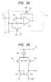
- FIG. 2A illustrates a circuit configuration of the comparing unit 3 according to the first embodiment of the present invention.
- the comparing unit 3 includes a comparator 21, an FB switch 22, a TH switch 23, a first input capacitor 24 and a second input capacitor 25.
- the comparator 21 includes two differential input terminals of a non-inverting input terminal and an inverting input terminal, and one output terminal.
- the comparator 21 has positive and negative power supply terminals which supply an electric power, but the illustration is omitted in the figure.
- One end of the FB switch 22 is connected to the output terminal of the comparator 21, and the other end is connected to the inverting input terminal of the comparator 21 and one end of the first input capacitor 24.
- the other end of the first input capacitor 24 is connected to the inverting input terminal of the comparator 21 and the FB switch 22, and the other end is connected to the output line 13 of the readout circuit.
- the TH switch 23 and the second input capacitor 25 are connected in parallel, and respective one ends are connected to the non-inverting input terminal of the comparator 21.
- the RAMP wiring 11 is connected to the other ends of the TH switch 23 and the second input capacitor 25.
- the ON (conducting state) operation or OFF (non-conducting state) operation of the FB switch 22 is controlled by a control signal CFB, and the ON or OFF operation of the TH switch 23 is controlled by a control signal CTH.
- any one of the FB switch 22 and the TH switch 23 shall be turned ON when the potential of the control signal is set at High.
- FIG. 2B is a view illustrating a circuit configuration of the comparator 21.
- the comparator 21 includes transistors 143 and 144 which are P-channel type FETs (Field Effect Transistor), and transistors 145 and 146 which are N-channel type FETs.
- the comparator 21 is formed of a differential amplifier circuit which uses a current mirror circuit.
- a current source 140 which applies an electric current to the circuit is connected to a commonized source terminal of the transistors 143 and 144.
- the gate terminals of the transistors 143 and 144 constitute an inverting input terminal 142 and a non-inverting input terminal 141 of the comparator 21, respectively.
- a drain terminal and the gate terminal of a diode-connected transistor 145 are connected to the drain terminal of the transistor 143 of which the gate terminal is the non-inverting input terminal 141.
- the drain terminal of a transistor 146 is connected to the drain terminal of the transistor 144 of which the gate terminal is the inverting input terminal 142, and this connecting wire constitutes an output terminal OUT of the comparator 21.
- the gate terminals of the transistors 145 and 146 are connected to each other.
- FIG. 3 is a view illustrating a circuit configuration of the pixel, and a configuration of the readout circuit.
- a pixel 1a included in the pixel unit 1 includes a photoelectric conversion element 32, a reset transistor 34, a transfer transistor 35, a source follower transistor 36 and a pixel selecting transistor 37.
- the photoelectric conversion element 32 is an element such as a photodiode which receives light, then generates an electromotive force by photoelectric conversion, and accumulates an electric charge therein.
- a source terminal of the transfer transistor 35 is connected to the photoelectric conversion element 32.
- the drain terminal of the transfer transistor 35 is connected to a source terminal of the reset transistor and a gate terminal of the source follower transistor 36, and constitutes a floating diffusion FD.
- a pixel signal transfer signal PTX is input into a gate terminal of the transfer transistor 35. When the potential of the pixel signal transfer signal PTX is High, the transfer transistor 35 is turned ON, and the electric charge accumulated in the photoelectric conversion element 32 is transferred to the floating diffusion FD.
- the drain terminal of the reset transistor 34 is connected to a power supply voltage VDD, and a pixel reset signal PRES is input into the gate terminal.
- a pixel reset signal PRES is input into the gate terminal.
- a drain terminal of the source follower transistor 36 is also connected to the power supply voltage VDD, and the potential of the source terminal is determined according to the potential of the floating diffusion FD which is connected to the gate terminal.
- a drain terminal of the pixel selecting transistor 37 is connected to the source terminal of the source follower transistor 36, and the source terminal is connected to the output line 31 of the pixel signal.
- the pixel selecting transistor 37 is turned ON when the potential of the pixel selecting signal PSEL which is input into the gate terminal is High, and the potential of the source terminal of the source follower transistor 36 is output to the output line 31 of the pixel signal.
- the readout circuit 2 includes a current source 33 that is connected to the output line 31 of the pixel signal, to which the signal sent from the pixel 1a is output, and a column amplifier 38 having a -A times gain.
- a source follower circuit is formed of the source follower transistor 36 and the current source 33 in the readout circuit 2.
- a potential which is output to the output line 31 of the pixel signal equals the potential as that of the floating diffusion FD.
- the source follower circuit is formed of the source follower transistor 36, and accordingly a voltage corresponding to the potential of the floating diffusion FD is output to the output line 31 of the pixel signal. Accordingly, the reset signal (power supply voltage VDD) of the pixel is input into the column amplifier 38 through the output line 31 of the pixel signal until the transfer transistor 35 is turned ON, and the pixel signal according to the light quantity is input into the column amplifier 38 after the transfer transistor 35 has been turned ON. Thereby, the reset signal and the pixel signal are multiplied by a factor of - A, and are output from the column amplifier 38.
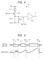
- FIG. 4 is a view illustrating a circuit configuration of the reference signal generating unit 6 which generates a ramp signal that functions as a reference signal.
- the reference signal generating unit 6 includes a current source 121, a charge capacitor 122, a charge switch 123, a discharge switch 124 and an output buffer 125.
- One end of the charge capacitor 122 is connected to one end of the charge switch 123, one end of the discharge switch 124 and the input terminal of the output buffer 125; and the other end is connected to the ground (GND).
- the other end of the charge switch 123 is connected to the current source 121.
- the other end of the discharge switch 124 is connected to the ground (GND).
- the output terminal of the output buffer 125 is connected to the RAMP wiring 11.
- the ON or OFF operation of the charge switch 123 is controlled by a charge switch control signal RMP_EN, and the ON or OFF operation of the discharge switch 124 is controlled by a discharge switch control signal RMP_RES. In the present description, both of the charge switch 123 and the discharge switch 124 shall be turned ON when the control signal is High.
- FIG. 5 is a timing chart illustrating an operation of the reference signal generating unit. A flow in which the reference signal generating unit 6 generates the ramp signal will be described below with reference to FIG. 5 .
- the potential of the charge switch control signal RMP_EN is Low
- the potential of the discharge switch control signal RMP_RES is High.
- the discharge switch 124 is connected to the ground. Accordingly, the electric charge is discharged to the charge capacitor 122, and the potential of the input of the output buffer 125 is the ground potential.
- the output buffer 125 outputs a potential corresponding to the input of the ground potential to the RAMP wiring 11, as the ramp signal.
- the potential at this time shall be represented by Vst.
- the potential of the discharge switch control signal RMP_RES becomes Low
- the potential of the charge switch control signal RMP_EN becomes High
- charging from the current source 121 to the charge capacitor 122 is started.
- the potential of the ramp signal increases as the electric charge is more accumulated in the charge capacitor 122.
- the potential of the charge switch control signal RMP_EN becomes Low, and the charging is completed.
- a period from the time T51 to the time T52 is a period in which a voltage for offset cancellation is generated.
- the potential of the RAMP wiring 11 is consistent with a voltage Vclmp for offset cancellation.
- the electric charge is not charged nor discharged in the charge capacitor 122, and accordingly the potential of the RAMP wiring 11 is held at Vclmp.
- the discharge switch control signal RMP_RES becomes High, and the electric charge which has been accumulated in the charge capacitor 122 is discharged. At this time, the potential of the RAMP wiring 11 becomes Vst.
- a period from the time T54 to the time T55 is a period in which the charge capacitor 122 is charged, and the ramp signal is generated of which the gradient is determined by the capacitance value of the charge capacitor 122 and the current value of the current source 121.
- the period from the time T54 to the time T55 is an A/D conversion period of the reset signal of the pixel 1a.
- the potential of the charge switch control signal RMP_EN becomes Low, and then the RAMP wiring 11 holds the potential at the time right before the potential of the charge switch control signal RMP_EN becomes Low, because the electric charge is not charged nor discharged in the charge capacitor 122.
- the potential of the discharge switch control signal RMP_RES becomes High, the electric charge which has been accumulated in the charge capacitor 122 is discharged, and the potential of the RAMP wiring 11 becomes Vst.
- the potential of the discharge switch control signal RMP_RES becomes Low, and the potential of the charge switch control signal RMP_EN becomes High.
- the potential of the charge switch control signal RMP_EN becomes Low.
- This period is a period in which the charge capacitor 122 is charged and the ramp signal is generated. This period is an A/D conversion period of the pixel signal.
- the potential of the discharge switch control signal RMP_RES becomes Low, and the potential of the RAMP wiring 11 becomes Vst.
- FIG. 6 is a timing chart illustrating an operation of the comparing unit 3 and a part of the pixel.
- the timing chart in FIG. 6 illustrates a relationship among voltages of each of the signals which are input and output from/to the comparing unit 3. Specifically, the timing chart illustrates the potentials and the timings of a pixel signal transfer signal PTX, a control signal CFB of the FB switch 22, a control signal CTH of the TH switch 23 and the ramp signal, as control signals to be input.
- the timing chart illustrates a relationship among the output voltage of the output line 31 of the pixel signal, the output voltage of the readout circuit 2, and the voltages of the inverting input terminal, the non-inverting input terminal and the output terminal of the comparator 21, as the relationship among the voltages of each of the corresponding wiring.
- the timing chart omits the illustration of the control signals PSEL and PRES in the pixel 1a, and the control signals RMP_EN and RMP_RES in the reference signal generating unit 6.
- the timing chart of FIG. 6 shows a period after the pixel 1a has been reset and when and after the ramp signal is outputting the voltage Vclmp.
- the reset signal of the pixel 1a is output to the output line 31 of the pixel signal.
- the signal is multiplied by a factor of -A, in the column amplifier 38 in the readout circuit 2, and the multiplied signal is output from the readout circuit 2.
- the potential of the output line 31 of the pixel signal shall be represented by Vpixn
- the potential of the output line 13 of the readout circuit shall be represented by Vn.
- the control signal CFB of the FB switch 22 and the control signal CTH of the TH switch 23 are shifted to High from Low.
- the output of the ramp signal is a potential Vclmp for offset cancellation.
- the FB switch 22 is turned ON.
- the inverting input terminal and the output terminal of the comparator 21 are short-circuited, and accordingly the comparing unit 3 assumes a structure of a voltage follower. Accordingly, the voltages of the output terminal and the inverting input terminal are consistent with a voltage of the non-inverting input terminal, specifically, are consistent with a voltage in which a voltage Vclmp and an offset voltage Vofs of the comparator itself are added.
- a potential difference across the first input capacitor 24 is Vclmp + Vofs - Vn which is a potential difference between the voltage of the inverting input terminal and the reset signal voltage Vn.
- the potential of the control signal CFB of the FB switch 22 is shifted at the time T2, and the potential of the signal of the control signal CTH of the TH switch 23 is shifted at the time T3, in this order, to Low from High.
- the CFB becomes Low
- the FB switch 22 is turned OFF, and accordingly Vclmp + Vofs - Vn is held which is the potential difference across the first input capacitor 24.
- the TH switch 23 is turned OFF, and accordingly a potential difference across the second input capacitor 25 is held at 0.
- the potential of the ramp signal falls to Vst.
- the A/D conversion of the reset signal of the pixel 1a is started.
- the potential of the pixel signal transfer signal PTX is shifted to High from Low, and then the pixel signal is output to the output line 31 of the pixel signal.
- the potential of the output line 31 of the pixel signal at this time shall be represented by Vpixs.
- the potential of the output line 31 of the pixel signal is multiplied by the factor of -A, in the column amplifier 38 of the readout circuit 2.
- a potential Vs corresponding to the pixel signal is output to the output line 13 of the readout circuit from the readout circuit 2.
- the potential Vpixs becomes smaller as the quantity of light incident on the pixel 1a becomes larger.
- the potential which is output to the output line 13 of the readout circuit increases by a value of Vs - Vn, and accordingly the potential of the inverting input terminal of the comparator 21 is Vclmp + Vofs + Vs - Vn.
- the A/D conversion of the pixel signal is started.
- the potential of the non-inverting input terminal exceeds Vclmp + Vofs + Vs - Vn
- the potential of the output of the comparator is shifted to High from Low, and the digital data of the pixel signal is stored in the storage unit 4.
- the A/D conversion of the pixel signal ends.
- the potential of the ramp signal is returned to Vst again.
- the signal processing circuit 8 acquires a difference of the digital data between the pixel signal and the reset signal which are stored in the storage unit 4, and outputs the difference.
- the A/D conversion of the pixel 1a ends.
- the lower limit value of the potential of the signal which is output from the readout circuit 2 and is input into the comparing unit 3 is a potential Vn which corresponds to the output of the readout circuit in the case where the potential of the reset signal of the pixel 1a is Vpixn.
- the potential which is input into the inverting input terminal of the comparator 21 during the A/D conversion period of this reset signal is the lower limit of the potential with which the comparator 21 should compare, and the potential serves as the lower limit in the input voltage range of the comparator 21.
- the potential of the inverting input terminal at the time when the offset is canceled is Vclmp + Vofs as has been described above.
- the potential of the output of the readout circuit 2 does not change from the potential at the time when the offset has been canceled and holds Vn, and accordingly the potential of the inverting input terminal of the comparator 21 holds Vclmp + Vofs. Because a relationship of Vs ⁇ Vn holds, the potential of the inverting input terminal of the comparator 21 is Vclmp + Vofs or larger during the A/D conversion period of the pixel signal.
- this value Vclmp + Vofs is the lower limit value of the input voltage with which the comparator 21 should compare.
- the lower limit value in the input voltage range of the comparator 21 is Vclmp.
- a dashed dotted line shown in the inverting input terminal of the timing chart is the lower limit value Vgs + Vofs of the input voltage in a conventional example which will be described later. Accordingly, in the present exemplary embodiment, if Vclmp is set to be smaller than Vgs, the input voltage range can be set to be larger than that in the conventional example, by a potential difference between Vgs and Vclmp.
- FIG. 7 is a view illustrating a circuit configuration of a comparing unit in a comparative example in which the offset cancellation is performed.
- a comparing unit 58 includes a comparator 21, diode switches 51a and 51b, and input capacitors 56 and 57.
- the comparator 21 includes transistors 52 and 53 which are P-channel type MOSFETs, and transistors 54 and 55 which are N-channel type MOSFETs.
- the comparator 21 is formed of a differential amplifier circuit which uses the current mirror circuit.
- This differential amplifier circuit is the current mirror circuit which has the P-channel type transistors 52 and 53 arranged in the differential input side, and has the Nch-channel type transistors 54 and 55 connected to the drain terminals of the transistors 52 and 53 that are differential input transistors.
- a current source 140 which applies an electric current to the circuit is connected to a commonized source terminal of the transistors 52 and 53.
- the drain terminals of the transistors 52 and 53 are connected to the drain terminals of the transistors 54 and 55, respectively.
- the gate terminal of one transistor 52 of the differential input transistors is a non-inverting input terminal of the comparator 21, and the gate terminal of the other transistor 53 thereof is an inverting input terminal of the comparator 21.
- the non-inverting input terminal of the comparator 21 is connected to the RAMP wiring 11 through an input capacitor 56, and the inverting input terminal is connected to the output line 13 of the readout circuit through an input capacitor 57.
- a diode switch 51a is connected between the gate terminal and the drain terminal of the transistor 52, and a diode switch 51b is connected between the gate terminal and the drain terminal of the transistor 53.
- the connecting point in between the drain terminal of the transistor 53 and the drain terminal of the transistor 55 constitutes an output terminal OUT of the comparing unit 58, and is connected to the storage unit 4.
- the source terminal of the transistors 54 and 55 is connected to the ground (GND).
- the gate terminal and the drain terminal of the transistor 54 are connected to each other, and the transistor 54 assumes a diode-connected structure.
- FIG. 8 is a timing chart illustrating an operation of the comparing unit in the comparative example.
- the operation of the comparing unit 58 according to the comparative example is similar to the above description, except the time when the offset voltage is charged in the capacitor, and accordingly the description will be omitted.
- T21 when the voltage of the control signal CFB of the diode switches 51a and 51b become High, the offset cancellation operation is started.
- the diode switches 51a and 51b are turned ON, and the gate terminal and the drain terminal of each of the transistors 52 and 53 are connected to each other to form diode connection.
- the potential of the non-inverting input terminal specifically, the potential of the gate terminal of the transistor 52 coincides with the potential difference Vgs between the gate and the source of the transistor 54.
- the potential of the inverting input terminal is Vgs + Vofs in which an offset voltage Vofs occurring due to the variation of the transistors 53 and 55 with respect to the transistors 52 and 54 is also added to Vgs.
- the potential of the ramp signal in the period from T21 to T22 is represented by Vclmp2
- the potential difference of Vgs - Vclmp2 is held in the input capacitor 56 in the non-inverting input terminal side
- the potential difference of Vgs + Vofs - Vn is held in the input capacitor 57 in the inverting input terminal side.
- the operations of the A/D conversion of the reset signal of the pixel 1a and the A/D conversion of the pixel signal are similar to the above description, and accordingly the description will be omitted.
- the potential of the inverting input terminal serves as the lower limit value in the input voltage range of the comparator 21, in the A/D conversion period of the reset signal of the pixel 1a.
- the offset voltage Vofs of the comparator is small and can be neglected.
- the lower limit value of the input voltage of the inverting input terminal of the comparator 21 is Vgs in the comparative example. This Vgs is determined by a semiconductor manufacturing condition and the amount of a drain current flowing in the transistor 54.
- the lower limit value of the input voltage is determined by the Vgs of the current mirror transistor.
- the lower limit value of the input voltage is determined by Vclmp. Therefore, if the voltage Vclmp for the offset cancellation of the ramp signal is set to be smaller than the Vgs of a current mirror transistor, the lower limit value in the input voltage range of the comparator 21 can be set to be small compared to that in the comparative example. Therefore, the input voltage range of the comparator is enlarged.
- the present invention is not limited to the configuration.
- the second input capacitor 25 may be omitted.
- the RAMP wiring 11 and the non-inverting input terminal of the comparator 21 are directly connected to each other.
- the circuit configuration of the pixel 1a and the circuit configuration of the readout circuit 2 have been described, but the present invention is not limited to those circuit configurations.
- the described circuit configuration of the reference signal generating unit 6 is one example, and the configuration is not limited to this. These circuits can be suitably changed so that a similar operation is obtained.
- the output buffer 125 may be omitted, and at the same time, the charge capacitor 122 may be directly connected to the RAMP wiring 12.
- the differential amplifier circuit illustrated in FIG. 2B has been illustrated and described as the circuit configuration of the comparator 21, but the present invention is not limited to the circuit.
- FIG. 9 is a view illustrating a configuration of an imaging system which uses the imaging apparatus according to the first embodiment of the present invention.
- An imaging system 800 includes an optical unit 810, an imaging apparatus 820, a recording & communicating unit 840, a timing control unit 850, a system control unit 860 and a playing & displaying unit 870.
- the imaging apparatus 820 includes the imaging apparatus 100, and a video signal processing unit 830. The above described imaging apparatus 100 is used for the imaging apparatus 100.
- the optical unit 810 composed of an optical system such as a lens focuses an image of light emitted from an object onto a pixel unit 1 of the imaging apparatus 100, in which a plurality of pixels is two-dimensionally arrayed, to form an image of the object on the pixel unit 1.
- the imaging apparatus 100 outputs signals according to the light imaged on the pixel unit 1, on the timing based on the signal output from the timing control unit 850.
- the signals output from the imaging apparatus 100 are input into the video signal processing unit 830.
- the video signal processing unit 830 performs signal processing such as the conversion of the input signal into image data, according to a specified method by a program.
- the signals resulting from the processing in the video signal processing unit 830 are sent to the recording & communicating unit 840 as image data.
- the recording & communicating unit 840 sends signals for forming an image to the playing & displaying unit 870, and makes the playing & displaying unit 870 play & display a moving image or a still image.
- the recording & communicating unit 840 also communicates with the system control unit 860 by receiving the signals sent from the video signal processing unit 830, and also performs an operation of recording the signals for forming an image on an unillustrated recording medium.
- the system control unit 860 is a unit for collectively controlling an operation of the imaging system, and controls a drive of each of the optical unit 810, the timing control unit 850, the recording & communicating unit 840, and the playing & displaying unit 870.
- the system control unit 860 is provided, for instance, with an unillustrated storage apparatus that is a recording medium, and records a program which is necessary for controlling the operation of the imaging system, in the storage apparatus.
- the system control unit 860 also supplies, for instance, a signal which switches driving modes according to an operation of a user, into the imaging system.
- the system control unit 860 supplies signals for switching, such as a change of a line to be read out or a line to be reset, a change of an angle of view, which accompanies an operation of an electronic zoom, and a shift of an angle of view, which accompanies electronic anti-vibration.
- the timing control unit 850 controls the driving timings for the imaging apparatus 100 and the video signal processing unit 830 based on the control by the system control unit 860.
- the comparing unit 3 which is provided in the imaging apparatus 100 according to the present embodiment has an enlarged input voltage range while decreasing the offset voltage. Specifically, the range of the voltage is enlarged which can be input at the time of the A/D conversion. Accordingly, the imaging system 800 can be achieved which can take an image with high precision by mounting the imaging apparatus 100 according to the present embodiment thereon.
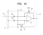
- FIG. 10 illustrates a circuit configuration of a comparing unit 73 which uses a comparator 21 according to the second embodiment of the present invention.
- the comparing unit 73 includes the comparator 21, an FB switch 22, a first input capacitor 24, a second input capacitor 25 and a potential supply switch 71.
- a fixed potential supply line 72 is connected to a non-inverting input terminal of the comparator 21 through the potential supply switch 71.
- one end of the second input capacitor 25 is connected in parallel with the fixed potential supply line 72.
- the RAMP wiring 11 is connected to the other end of the second input capacitor 25.
- the connection of an inverting input terminal and the output terminal of the comparator 21 is similar to that in the first embodiment.
- One end of the FB switch 22 is connected to the output terminal of the comparator 21, and the other end thereof is connected to the inverting input terminal of the comparator 21 and one end of the first input capacitor 24.
- the output line 13 of the readout circuit is connected to the other end of the first input capacitor 24.
- circuits other than the comparing unit 73, such as the readout circuit 2 are similar to those in the first embodiment.
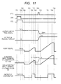
- FIG. 11 illustrates a timing chart for describing an operation of the present embodiment.
- both of the potentials becomes High, which are the potential of the control signal CFB of the FB switch 22 for controlling an ON or OFF operation of the FB switch 22, and the potential of the control signal CCL of the potential supply switch 71 for controlling an ON or OFF operation of the potential supply switch 71.
- the signal which is output from the pixel 1a is a reset signal, similarly to the case in the first embodiment.
- the comparator 21 assumes a structure of a voltage follower.
- Vcl the potential of the non-inverting input terminal of the comparator 21
- a potential difference across the first input capacitor 24 is Vcl + Vofs - Vn which is a potential difference between the potential Vcl + Vofs of the inverting input terminal and the potential Vn of the output line 13 of the readout circuit.
- a potential difference across the second input capacitor 25 is Vcl - Vclmp which is a potential difference between the potential Vcl of the fixed potential supply line 72 and the potential Vclmp of the ramp signal.
- the potential of the control signal CFB of the FB switch 22 becomes Low.
- the potential of the control signal CCL of the potential supply switch 71 becomes Low.
- the potential difference held in the first input capacitor 24 is Vcl + Vofs - Vn
- the potential difference held in the second input capacitor 25 is Vc1 - Vclmp.
- the potential of the inverting input terminal of the comparator 21 is Vcl + Vofs. Therefore, suppose that the offset voltage Vofs of the comparator is small and can be neglected, the lower limit of the voltage to be input into the comparator 21 is Vcl. Therefore, when the potential Vcl to be supplied from the fixed potential supply line 72 is set to be smaller than the voltage Vgs between the gate and the source in the above described comparative example, the input voltage range of the comparing unit 73 is enlarged.
- the potential is supplied from the RAMP wiring 11, and accordingly there is such a limitation that only a potential within a range in which the RAMP wiring 11 can output the ramp signal therethrough can be supplied.
- the potential is supplied from the fixed potential supply line 72 which is different from the RAMP wiring 11. Accordingly, the advantage of the second embodiment is a point that the fixed potential to be supplied to the non-inverting input terminal can be independently set without being restricted by the range in which the RAMP wiring 11 can output the signal therethrough.
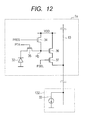
- FIG. 12 is a view illustrating a circuit configuration of a pixel 1a and a circuit configuration of a readout circuit 132 according to the third embodiment of the present invention.
- a point in which the third embodiment is different from the first and second embodiments is that the column amplifier of the readout circuit is omitted. Therefore, the previous output line 31 of the pixel signal is connected to the output line 13 of the readout circuit, and the potential of the output line 13 of the readout circuit is output intact as the potential of the output line 31 of the pixel signal.
- both of the wirings shall be integrally referred to as the output line 13 of the readout circuit. The other descriptions are similar to the above description, and accordingly the description will be omitted.
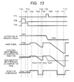
- FIG. 13 is a timing chart for describing an operation of the present embodiment.
- the potential of the ramp signal shows such a form that the ramp signal described in the exemplary embodiments 1 and 2 is vertically inverted, specifically, that the potential becomes smaller according to the elapse of the time.
- the output of the comparator 21 also shows such a waveform that the above described waveform is inverted, as is illustrated in FIG. 13 .
- the potential of the ramp signal can be inverted in this way, for instance, by a structure in which the output buffer 125 of the reference signal generating unit 6 is formed of a inverting amplifier circuit.
- the upper limit of the potential to be input into the comparator 21 in the present exemplary embodiment suppose that Vofs is small and can be neglected. Then, as has been described above, the upper limit value of the input voltage range of the comparator 21 is Vclmp.
- the upper limit of the input voltage is determined by Vgs which is a voltage between the gate and the source of the current mirror circuit that is formed of the N-channel type transistor. Accordingly, if Vclmp is set to be larger than Vgs, the input voltage range can be enlarged.
- the column amplifier having a negative amplification factor is omitted, and accordingly a voltage to be input to the comparing unit is vertically inverted with respect to the case of the first embodiment. Accordingly, as in the potential of the output line of the readout circuit in FIG. 13 , when the incident light quantity into the pixel 1a is large, the voltage to be input into the comparing unit becomes low, and when the incident light quantity is small, the voltage to be input into the comparing unit becomes high. This relationship is reverse to the case of the first embodiment.
- the transistor arranged in the input side of the comparing unit 3 has employed a P-channel type transistor which has a wide input range in the ground side.
- the circuit configuration can be changed so that the N-channel type transistor having a wide input range in a high-voltage side is used in the input side.
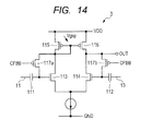
- FIG. 14 is a view illustrating another circuit configuration of a comparing unit in a comparative example, which is compared with the comparing unit 3 in the third embodiment of the present invention. A point different from the comparing unit illustrated in FIG. 7 will be described below.
- N-channel type transistors 113 and 114 are arranged in the differential input side.
- the drain terminals of P-channel type transistors 115 and 116 are connected to the drain terminals of the transistors 113 and 114, respectively.
- the arrangement of the N-channel type transistor and the P-channel type transistor is reverse to the arrangement of that in the comparing unit in FIG. 7 .
- the power supply potential VDD is connected to the source terminals of the P-channel type transistors 115 and 116, and the source terminals of the N-channel type transistors 113 and 114 are connected to the ground.
- a diode switch 117a is connected between the gate terminal and the drain terminal of the transistor 113, and a diode switch 117b is connected between the gate terminal and the drain terminal of the transistor 114. The diode switches 117a and 117b are turned ON when the potential of the control signal CFBB is Low.
- the operation of the comparing unit 3 is similar to that in the comparing unit illustrated in FIG. 7 , and accordingly the details will be omitted, but a point that the input voltage ranges are different from each other will be described below.
- the potential of the control signal CFBB becomes Low, and the differential input transistors 113 and 114 assume a structure of diode connection.
- the potential of the gate terminal of the transistor 113 is VDD - Vgsp
- the potential of the gate terminal of the transistor 114 is VDD - Vgsp + Vofs in which the offset voltage Vofs is added to VDD - Vgsp.
- Vgsp is a voltage between the gate and the source of the P-channel type transistor which constitutes the current mirror circuit.
- Vofs is small and can be neglected, in this configuration, the upper limit of the input voltage is VDD - Vgsp. Therefore, when Vclmp is set to be larger than VDD - Vgsp, the input voltage range is enlarged.
- the operation of the comparing unit 3 has been described on the assumption that the operation of the comparing unit 3 is similar to that of the comparing unit in the first embodiment, but the comparing unit 3 described in the second embodiment can also be applied.
- the potential Vcl which is supplied from the fixed potential supply line 72 is set to be larger than Vgs or VDD - Vgsp, the present embodiment can be configured so that a similar effect is shown.
- the column amplifier 38 is omitted, and accordingly it can be avoided that a noise generated in the column amplifier 38 is overlapped on the pixel signal.
- the number of the elements is reduced. Accordingly, an efficiency percentage is enhanced, and the area of the imaging apparatus can be reduced. Accordingly, it is advantageous in terms of both economical efficiency and reduction in the size.
- the output line 13 of the readout circuit is input directly into the comparing unit 3, but an inputting method in the present invention is not limited to the direct inputting method.
- a non-inverting amplifier may be arranged between the output line 13 of the readout circuit and the comparing unit 3. By doing so, the output signal potential can be amplified as needed, and the precision can be enhanced.
- the imaging apparatus 100 described in the first to third embodiments is not limited to the above described embodiments, and can be modified in various ways. One example thereof will be described below.
- the bypass path which is switched from another path can be achieved by adding a bypass circuit which uses a diode switch in parallel, and turning ON or turning OFF the diode switch by a control signal.
- the imaging apparatus can avoid a phenomenon that a noise generated in the column amplifier 38 is superimposed on the pixel signal, by directly giving the pixel signal to the comparing unit 3 without passing the signal through the column amplifier 38, when the incident light quantity is large.
- the imaging apparatus can amplify the pixel signal in the column amplifier 38, and then give the pixel signal to the comparing unit 3.
- an amplification ratio of the column amplifier 38 is negative, and accordingly the positive and negative values of the pixel signal and a reset signal are inverted when the circuit which outputs the signal through the column amplifier 38 is switched to the circuit which bypasses the column amplifier 38. Because of this, the imaging apparatus needs to be configured to vertically invert the ramp signal at the same time when having switched the circuit to the bypass circuit, according to the same method as that in the description of the third embodiment.
- the imaging apparatus can be configured not only so as to vertically invert the ramp signal but also change a potential value of the ramp signal such as a starting voltage, when having switched the circuit to the circuit which bypasses the column amplifier 38.
- the amplitude of the reset signal is small, and accordingly the voltage of the reset signal becomes close to a power supply voltage or the ground voltage. If the starting voltage of the ramp signal is constant, a difference between the starting voltage of the ramp signal and an output voltage of the reset signal becomes very large in any one of modes in the case where the column amplifier 38 is bypassed and in the case where the column amplifier 38 is not bypassed.
- the imaging apparatus can be configured so as to change the starting voltage of the ramp signal as well, when having switched between a circuit which bypasses the column amplifier 38 and a circuit which does not.
- non-inverting amplifier which has a positive voltage amplification ratio as the column amplifier 38 so that the positive and negative values of the pixel signal and the reset signal are not reversed in the case where the column amplifier 38 is bypassed or in the case where the column amplifier 38 is not bypassed.
- the imaging system can be configured so that the above described switching operation is performed based on ISO sensitivity.
- the imaging apparatus may be configured so as to switch between the presence and absence of the bypass, as a method of making the signal bypass the column amplifier 38 when the ISO sensitivity is low, and amplifying the signal in the column amplifier 38 when the ISO sensitivity is high.
- the configuration is not limited to a switching method using a switch, but can be achieved by various configurations which can obtain a predetermined amplification ratio. For instance, a similar effect can be obtained also by a configuration of controlling the amplification ratio so that the amplification ratio is changed by using the column amplifier 38 of which the amplification ratio is variable.
- the RAMP wiring 11 into which the ramp signal is input has been connected to the comparator 21 through the input capacitor 25, but the present invention is not limited to the configuration.
- a buffer which is formed of a source follower circuit may be arranged between the RAMP wiring 11 and the input capacitor 25.
- the configuration is also usable that has a plurality of stages by arranging a gain stage formed of an amplifier circuit using a transistor in the output of the comparator, which constitute a common source circuit, for instance.
- the comparator according to the present exemplary embodiment can have an input voltage range larger than the case where a conventional offset cancel technique is used, while reducing an offset voltage of a comparator circuit.
- An object of the present invention is to provide a comparator which has an input voltage range larger than the case where a conventional offset cancel technique is used, while reducing an offset voltage.
- a comparator circuit includes: a comparator having an inverting input terminal, a non-inverting input terminal and an output terminal; a first switch having one terminal connected to the inverting input terminal and having the other terminal connected to the output terminal; a first capacitor which has one end connected with the inverting input terminal; a first signal input terminal which is another end of the first capacitor; and a second signal input terminal which selectively inputs either one of a fixed voltage and a comparing signal into the non-inverting input terminal.
Abstract
Description
- The present invention relates to a comparator circuit, an imaging apparatus using the same, and a method of controlling the comparator circuit.
- Generally, a configuration of an analog-digital (A/D) converter includes a comparator. The A/D converter is used, for instance, for an imaging apparatus. For the imaging apparatus, there is a technique of connecting the A/D converter to each column of pixels arranged in rows and columns, and converting an analog signal output from each of the pixels into digital data by the A/D converter. Some A/D converters include a differential-input and single-end-output type comparator. There is a variation of offset voltage between input terminals of each of the comparators, among each of the columns. As a method of reducing this variation, a technique is known which cancels an offset voltage as described in Japanese Patent Application Laid-Open No.
2010-16656 - However, in an offset voltage canceling method described in Japanese Patent Application Laid-Open No.
2010-16656 - According to an aspect of the present invention, a comparator circuit comprises: a comparator having an inverting input terminal, a non-inverting input terminal and an output terminal; a first switch having terminals, one terminal of the terminals connected to the inverting terminal, the other terminal of the terminals connected to the output terminal; a first capacitor having terminals, one terminal of the terminals receiving an analog signal, the other terminal of the terminals being connected to the inverting input terminal and the one terminal of the first switch; a second capacitor having terminals, one terminal of the terminals being connected to the non-inverting terminal, the other terminal of the terminals receiving a comparing signal; and a second switch having terminals, one terminal of the terminals being connected to the one terminal of the second capacitor and the non-inverting terminal, the other terminal of the terminals receiving a fixed voltage.
- Further features of the present invention will become apparent from the following description of exemplary embodiments with reference to the attached drawings.
-
-
FIG. 1 is a schematic view illustrating a circuit configuration of an imaging apparatus according to a first embodiment of the present invention. -
FIGS. 2A and 2B are views illustrating a circuit configuration of a comparing unit (A) and a comparator (B) according to the first embodiment of the present invention. -
FIG. 3 is a view illustrating a circuit configuration of a pixel and a configuration of a readout circuit according to the first embodiment of the present invention. -
FIG. 4 is a view illustrating a circuit configuration of a reference signal generating unit according to the first embodiment of the present invention. -
FIG. 5 is a timing chart illustrating an operation of the reference signal generating unit according to the first embodiment of the present invention. -
FIG. 6 is a timing chart illustrating an operation of the comparing unit according to the first embodiment of the present invention. -
FIG. 7 is a view illustrating a circuit configuration of the comparing unit for describing a comparative example. -
FIG. 8 is a timing chart illustrating an operation of the comparing unit in the comparative example. -
FIG. 9 is a view illustrating a configuration of an imaging system which uses the imaging apparatus according to the first embodiment of the present invention. -
FIG. 10 is a view illustrating a configuration of a comparing unit according to a second embodiment of the present invention. -
FIG. 11 is a timing chart illustrating an operation of the comparing unit according to the second exemplary embodiment of the present invention. -
FIG. 12 is another view illustrating a circuit configuration of a pixel and a configuration of a readout circuit. -
FIG. 13 is a timing chart illustrating an operation of a comparing unit according to a third exemplary embodiment of the present invention. -
FIG. 14 is a view illustrating another circuit configuration of the comparing unit for describing the comparative example. - Preferred embodiments of the present invention will now be described in detail in accordance with the accompanying drawings.
- An imaging apparatus according to a first embodiment of the present invention and a comparator which is included in an A/D converter provided in each column of the imaging apparatus will be described below.
FIG. 1 is a schematic view illustrating a circuit configuration of an imaging apparatus according to the first embodiment of the present invention. Animaging apparatus 100 includes: apixel unit 1, a plurality ofreadout circuits 2, a plurality of comparingunits 3, a plurality ofstorage units 4, ahorizontal scanning circuit 5, a referencesignal generating unit 6, a counter circuit 7, and a signal processing circuit 8. - The
pixel unit 1 includes a plurality of pixels arranged in rows and columns. Each of the pixels outputs signals to a plurality ofoutput lines 31 of the pixel signal, which is arranged for every pixel line, respectively. - Each of the
readout circuits 2 is connected to each of the pixel columns in thepixel unit 1 through each of theoutput lines 31 of the pixel signal, and receives input signals. Each of thereadout circuits 2 receives the input signal from thepixel unit 1, subjects the signal to the processing of amplification, and outputs the processed signal to the signal input terminal of each of the comparingunits 3 by each of the readoutsignal output lines 13. - The reference
signal generating unit 6 selectively generates any one of a fixed voltage and a ramp signal that is a comparing signal, which are used as the reference signal at the time of the A/D conversion; and outputs the generated signal to each of the comparingunits 3 through aRAMP wiring 11. The ramp signal has a waveform such as a saw-tooth wave, which represents the potential monotonically increasing or decreasing over time. - Each of the comparing
units 3 is a comparator circuit which includes a differential-input and single-end-output type comparator. Each of thecomparing units 3 has two differential signal input terminals and one signal output terminal, and the terminals are connected to the differential input terminals and the output terminal of the comparator, respectively. One of the differential input terminals of the comparingunit 3 is connected to each of thereadout circuits 2 by theoutput line 13 of the readout circuit, and the other end is connected to the referencesignal generating unit 6 through theRAMP wiring 11. Each of the comparingunits 3 compares the signal input from theoutput line 13 of the readout circuit with the ramp signal input from theRAMP wiring 11, and outputs the signal according to the comparison result to each of thestorage units 4. - Each of the
storage units 4 is connected to the output terminal of each of the comparingunits 3, thehorizontal scanning circuit 5, the counter circuit 7, and the signal processing circuit 8. Each of thestorage units 4 converts the output signal from each of the comparingunits 3 into digital data, with reference to a counter signal input from the counter circuit 7, and stores the converted digital data therein. The digital data stored in each of thestorage units 4 is transferred to the signal processing circuit 8 based on a signal sent from thehorizontal scanning circuit 5, and is subjected to signal processing. - Next, the outline of the A/D conversion which is performed in the circuit of the
imaging apparatus 100 will be described. The output signal of thereadout circuit 2 is input into one differential input terminal of thecomparing unit 3, and the ramp signal which is generated in the referencesignal generating unit 6 is input into the other differential input terminal, through theRAMP wiring 11. The comparingunit 3 compares the potential of the signal output from thereadout circuit 2 with the potential of the ramp signal, and outputs a signal having a potential of a High level or a Low level to thestorage unit 4 according to the comparison result. When the relationship of the magnitude between the potential of the signal output from thereadout circuit 2 and the potential of the ramp signal which changes with the time is inverted, the potential of the signal which is output to thestorage unit 4 from the comparingunit 3 is shifted to Low from High or High from Low. On the other hand, the counter circuit 7 outputs a count value which changes with the time, to each of thestorage units 4 through acount data wiring 12. Thestorage unit 4 stores the counter value which is output from the counter circuit 7 as the digital data therein, at such a timing that the output potential of the comparingunit 3 is inverted. In this way, the A/D conversion is accomplished which converts the signal output from thereadout circuit 2 into the digital data and stores the converted digital data in thestorage unit 4. - The reset signal and the pixel signal in each of the pixels are subjected to this A/D conversion, and are converted into the digital data. The digital data stored in the
storage unit 4 is sequentially transferred to the signal processing circuit 8 in each of the pixel columns, in response to the signal output from thehorizontal scanning circuit 5. The signal processing circuit 8 performs the signal processing to acquire a difference between digital data corresponding to the reset signal and digital data corresponding to the pixel signal. Thereby, digital CDS (digital correlated double sampling) is achieved. -
FIG. 2A illustrates a circuit configuration of the comparingunit 3 according to the first embodiment of the present invention. The comparingunit 3 includes acomparator 21, anFB switch 22, aTH switch 23, afirst input capacitor 24 and asecond input capacitor 25. - The
comparator 21 includes two differential input terminals of a non-inverting input terminal and an inverting input terminal, and one output terminal. In addition, thecomparator 21 has positive and negative power supply terminals which supply an electric power, but the illustration is omitted in the figure. One end of theFB switch 22 is connected to the output terminal of thecomparator 21, and the other end is connected to the inverting input terminal of thecomparator 21 and one end of thefirst input capacitor 24. The other end of thefirst input capacitor 24 is connected to the inverting input terminal of thecomparator 21 and theFB switch 22, and the other end is connected to theoutput line 13 of the readout circuit. TheTH switch 23 and thesecond input capacitor 25 are connected in parallel, and respective one ends are connected to the non-inverting input terminal of thecomparator 21. TheRAMP wiring 11 is connected to the other ends of theTH switch 23 and thesecond input capacitor 25. The ON (conducting state) operation or OFF (non-conducting state) operation of theFB switch 22 is controlled by a control signal CFB, and the ON or OFF operation of theTH switch 23 is controlled by a control signal CTH. Incidentally, in the description of the present embodiment, any one of theFB switch 22 and theTH switch 23 shall be turned ON when the potential of the control signal is set at High. -
FIG. 2B is a view illustrating a circuit configuration of thecomparator 21. Thecomparator 21 includestransistors transistors comparator 21 is formed of a differential amplifier circuit which uses a current mirror circuit. Acurrent source 140 which applies an electric current to the circuit is connected to a commonized source terminal of thetransistors transistors input terminal 142 and anon-inverting input terminal 141 of thecomparator 21, respectively. A drain terminal and the gate terminal of a diode-connectedtransistor 145 are connected to the drain terminal of thetransistor 143 of which the gate terminal is thenon-inverting input terminal 141. The drain terminal of atransistor 146 is connected to the drain terminal of thetransistor 144 of which the gate terminal is the invertinginput terminal 142, and this connecting wire constitutes an output terminal OUT of thecomparator 21. In addition, the gate terminals of thetransistors -
FIG. 3 is a view illustrating a circuit configuration of the pixel, and a configuration of the readout circuit. Apixel 1a included in thepixel unit 1 includes aphotoelectric conversion element 32, areset transistor 34, atransfer transistor 35, asource follower transistor 36 and apixel selecting transistor 37. - The
photoelectric conversion element 32 is an element such as a photodiode which receives light, then generates an electromotive force by photoelectric conversion, and accumulates an electric charge therein. - A source terminal of the
transfer transistor 35 is connected to thephotoelectric conversion element 32. The drain terminal of thetransfer transistor 35 is connected to a source terminal of the reset transistor and a gate terminal of thesource follower transistor 36, and constitutes a floating diffusion FD. A pixel signal transfer signal PTX is input into a gate terminal of thetransfer transistor 35. When the potential of the pixel signal transfer signal PTX is High, thetransfer transistor 35 is turned ON, and the electric charge accumulated in thephotoelectric conversion element 32 is transferred to the floating diffusion FD. - The drain terminal of the
reset transistor 34 is connected to a power supply voltage VDD, and a pixel reset signal PRES is input into the gate terminal. When the potential of the pixel reset signal PRES is High, thereset transistor 34 is turned ON, and the potential of the floating diffusion FD is consistent with the power supply voltage VDD. - A drain terminal of the
source follower transistor 36 is also connected to the power supply voltage VDD, and the potential of the source terminal is determined according to the potential of the floating diffusion FD which is connected to the gate terminal. - A drain terminal of the
pixel selecting transistor 37 is connected to the source terminal of thesource follower transistor 36, and the source terminal is connected to theoutput line 31 of the pixel signal. Thepixel selecting transistor 37 is turned ON when the potential of the pixel selecting signal PSEL which is input into the gate terminal is High, and the potential of the source terminal of thesource follower transistor 36 is output to theoutput line 31 of the pixel signal. - The
readout circuit 2 includes acurrent source 33 that is connected to theoutput line 31 of the pixel signal, to which the signal sent from thepixel 1a is output, and acolumn amplifier 38 having a -A times gain. In a row corresponding to the readout row out of a plurality of pixel rows, the potential of the pixel selecting signal PSEL which is applied to thepixel selecting transistor 37 is High, and thepixel selecting transistor 37 is turned ON. At this time, a source follower circuit is formed of thesource follower transistor 36 and thecurrent source 33 in thereadout circuit 2. In other words, a potential which is output to theoutput line 31 of the pixel signal equals the potential as that of the floating diffusion FD. - An operation of the circuit at the time when the signal is read out will be described below. When the potential of the pixel reset signal PRES is set at High and the
reset transistor 34 is turned ON, the potential of the floating diffusion FD equals the potential as that of the power supply voltage VDD, and the circuit is reset. Next, the potential of the pixel reset signal PRES is set at Low, and thereset transistor 34 is turned OFF. After that, the potential of the pixel signal transfer signal PTX is set at High, and thetransfer transistor 35 is turned ON. Then, the electric charge accumulated in thephotoelectric conversion element 32 is transferred to the floating diffusion FD. - The potential which is output in the above described circuit operation will be described below. The source follower circuit is formed of the
source follower transistor 36, and accordingly a voltage corresponding to the potential of the floating diffusion FD is output to theoutput line 31 of the pixel signal. Accordingly, the reset signal (power supply voltage VDD) of the pixel is input into thecolumn amplifier 38 through theoutput line 31 of the pixel signal until thetransfer transistor 35 is turned ON, and the pixel signal according to the light quantity is input into thecolumn amplifier 38 after thetransfer transistor 35 has been turned ON. Thereby, the reset signal and the pixel signal are multiplied by a factor of - A, and are output from thecolumn amplifier 38. -
FIG. 4 is a view illustrating a circuit configuration of the referencesignal generating unit 6 which generates a ramp signal that functions as a reference signal. The referencesignal generating unit 6 includes acurrent source 121, acharge capacitor 122, acharge switch 123, adischarge switch 124 and anoutput buffer 125. - One end of the
charge capacitor 122 is connected to one end of thecharge switch 123, one end of thedischarge switch 124 and the input terminal of theoutput buffer 125; and the other end is connected to the ground (GND). The other end of thecharge switch 123 is connected to thecurrent source 121. The other end of thedischarge switch 124 is connected to the ground (GND). The output terminal of theoutput buffer 125 is connected to theRAMP wiring 11. The ON or OFF operation of thecharge switch 123 is controlled by a charge switch control signal RMP_EN, and the ON or OFF operation of thedischarge switch 124 is controlled by a discharge switch control signal RMP_RES. In the present description, both of thecharge switch 123 and thedischarge switch 124 shall be turned ON when the control signal is High. -
FIG. 5 is a timing chart illustrating an operation of the reference signal generating unit. A flow in which the referencesignal generating unit 6 generates the ramp signal will be described below with reference toFIG. 5 . In a period before the time T51, the potential of the charge switch control signal RMP_EN is Low, and the potential of the discharge switch control signal RMP_RES is High. Thedischarge switch 124 is connected to the ground. Accordingly, the electric charge is discharged to thecharge capacitor 122, and the potential of the input of theoutput buffer 125 is the ground potential. Theoutput buffer 125 outputs a potential corresponding to the input of the ground potential to theRAMP wiring 11, as the ramp signal. The potential at this time shall be represented by Vst. - At the time T51, the potential of the discharge switch control signal RMP_RES becomes Low, the potential of the charge switch control signal RMP_EN becomes High, and charging from the
current source 121 to thecharge capacitor 122 is started. In a period from the time T51 to the time T52, the potential of the ramp signal increases as the electric charge is more accumulated in thecharge capacitor 122. - At the time T52, the potential of the charge switch control signal RMP_EN becomes Low, and the charging is completed. A period from the time T51 to the time T52 is a period in which a voltage for offset cancellation is generated. At the time T52, the potential of the
RAMP wiring 11 is consistent with a voltage Vclmp for offset cancellation. In a period from the time T52 to the time T53, the electric charge is not charged nor discharged in thecharge capacitor 122, and accordingly the potential of theRAMP wiring 11 is held at Vclmp. - In a period from the time T53 to the time T54, the discharge switch control signal RMP_RES becomes High, and the electric charge which has been accumulated in the
charge capacitor 122 is discharged. At this time, the potential of theRAMP wiring 11 becomes Vst. - At the time T54, the potential of the discharge switch control signal RMP_RES becomes Low, and the potential of the charge switch control signal RMP_EN becomes High. At the time T55, the potential of the charge switch control signal RMP_EN becomes Low. A period from the time T54 to the time T55 is a period in which the
charge capacitor 122 is charged, and the ramp signal is generated of which the gradient is determined by the capacitance value of thecharge capacitor 122 and the current value of thecurrent source 121. The period from the time T54 to the time T55 is an A/D conversion period of the reset signal of thepixel 1a. - At the time T55, the potential of the charge switch control signal RMP_EN becomes Low, and then the
RAMP wiring 11 holds the potential at the time right before the potential of the charge switch control signal RMP_EN becomes Low, because the electric charge is not charged nor discharged in thecharge capacitor 122. - In a period from the time T56 to the time T57, the potential of the discharge switch control signal RMP_RES becomes High, the electric charge which has been accumulated in the
charge capacitor 122 is discharged, and the potential of theRAMP wiring 11 becomes Vst. After that, at the time T57, the potential of the discharge switch control signal RMP_RES becomes Low, and the potential of the charge switch control signal RMP_EN becomes High. At the time T58, the potential of the charge switch control signal RMP_EN becomes Low. This period is a period in which thecharge capacitor 122 is charged and the ramp signal is generated. This period is an A/D conversion period of the pixel signal. After that, at the time T59, the potential of the discharge switch control signal RMP_RES becomes Low, and the potential of theRAMP wiring 11 becomes Vst. -
FIG. 6 is a timing chart illustrating an operation of the comparingunit 3 and a part of the pixel. The timing chart inFIG. 6 illustrates a relationship among voltages of each of the signals which are input and output from/to the comparingunit 3. Specifically, the timing chart illustrates the potentials and the timings of a pixel signal transfer signal PTX, a control signal CFB of theFB switch 22, a control signal CTH of theTH switch 23 and the ramp signal, as control signals to be input. In addition, the timing chart illustrates a relationship among the output voltage of theoutput line 31 of the pixel signal, the output voltage of thereadout circuit 2, and the voltages of the inverting input terminal, the non-inverting input terminal and the output terminal of thecomparator 21, as the relationship among the voltages of each of the corresponding wiring. Incidentally, the timing chart omits the illustration of the control signals PSEL and PRES in thepixel 1a, and the control signals RMP_EN and RMP_RES in the referencesignal generating unit 6. In addition, the timing chart ofFIG. 6 shows a period after thepixel 1a has been reset and when and after the ramp signal is outputting the voltage Vclmp. - In an initial state, specifically, before the time T1, the reset signal of the
pixel 1a is output to theoutput line 31 of the pixel signal. The signal is multiplied by a factor of -A, in thecolumn amplifier 38 in thereadout circuit 2, and the multiplied signal is output from thereadout circuit 2. At this time, the potential of theoutput line 31 of the pixel signal shall be represented by Vpixn, and the potential of theoutput line 13 of the readout circuit shall be represented by Vn. - At the time T1, the control signal CFB of the
FB switch 22 and the control signal CTH of theTH switch 23 are shifted to High from Low. At this time, the output of the ramp signal is a potential Vclmp for offset cancellation. When the potential of the control signal CFB of theFB switch 22 is High, theFB switch 22 is turned ON. The inverting input terminal and the output terminal of thecomparator 21 are short-circuited, and accordingly the comparingunit 3 assumes a structure of a voltage follower. Accordingly, the voltages of the output terminal and the inverting input terminal are consistent with a voltage of the non-inverting input terminal, specifically, are consistent with a voltage in which a voltage Vclmp and an offset voltage Vofs of the comparator itself are added. At this time, a potential difference across thefirst input capacitor 24 is Vclmp + Vofs - Vn which is a potential difference between the voltage of the inverting input terminal and the reset signal voltage Vn. - After that, the potential of the control signal CFB of the
FB switch 22 is shifted at the time T2, and the potential of the signal of the control signal CTH of theTH switch 23 is shifted at the time T3, in this order, to Low from High. When the CFB becomes Low, theFB switch 22 is turned OFF, and accordingly Vclmp + Vofs - Vn is held which is the potential difference across thefirst input capacitor 24. In addition, when the potential of the control signal CTH of theTH switch 23 becomes Low, theTH switch 23 is turned OFF, and accordingly a potential difference across thesecond input capacitor 25 is held at 0. - After that, at the time T4, the potential of the ramp signal falls to Vst. At the time T5, the A/D conversion of the reset signal of the
pixel 1a is started. - At the time T6, when the potential of the signal which is input into the non-inverting input terminal of the
comparator 21 exceeds the voltage Vclmp + Vofs held at the inverting input terminal, the potential of the output of the comparator is shifted to High from Low. The count value at this time is stored in thestorage unit 4 as the digital data of the reset signal, and thereby the input signal is subjected to the A/D conversion. After that, at the time T7, the A/D conversion period of the reset signal ends. At the time T8, the potential of the ramp signal falls to Vst again. - After that, at the time T9, the potential of the pixel signal transfer signal PTX is shifted to High from Low, and then the pixel signal is output to the
output line 31 of the pixel signal. The potential of theoutput line 31 of the pixel signal at this time shall be represented by Vpixs. The potential of theoutput line 31 of the pixel signal is multiplied by the factor of -A, in thecolumn amplifier 38 of thereadout circuit 2. Then, a potential Vs corresponding to the pixel signal is output to theoutput line 13 of the readout circuit from thereadout circuit 2. Here, the potential Vpixs becomes smaller as the quantity of light incident on thepixel 1a becomes larger. When the light is not incident on thepixel 1a, a relationship of Vpixs = Vpixn holds. On the other hand, the output of thereadout circuit 2 is amplified by thecolumn amplifier 38 which is the inverting amplifier having the -A times gain, and the positive and negative potentials are inverted. Accordingly, the potential Vs becomes high according to the light quantity. In addition, when the light is not incident on thepixel 1a, a relationship of Vs = Vn holds, and the minimal value of the potential which is output from thereadout circuit 2 becomes Vn. Accordingly, when the pixel signal is output to theoutput line 31 of the pixel signal, the potential which is output to theoutput line 13 of the readout circuit increases by a value of Vs - Vn, and accordingly the potential of the inverting input terminal of thecomparator 21 is Vclmp + Vofs + Vs - Vn. - After that, at the time T10, the A/D conversion of the pixel signal is started. At the time T11, when the potential of the non-inverting input terminal exceeds Vclmp + Vofs + Vs - Vn, the potential of the output of the comparator is shifted to High from Low, and the digital data of the pixel signal is stored in the
storage unit 4. At the time T12, the A/D conversion of the pixel signal ends. At the time T13, the potential of the ramp signal is returned to Vst again. At this time, the signal processing circuit 8 acquires a difference of the digital data between the pixel signal and the reset signal which are stored in thestorage unit 4, and outputs the difference. Thus, the A/D conversion of thepixel 1a ends. - Next, the lower limit in the input voltage range of the
comparator 21 during the operation of the above described comparingunit 3 will be described. As described above, the lower limit value of the potential of the signal which is output from thereadout circuit 2 and is input into the comparingunit 3 is a potential Vn which corresponds to the output of the readout circuit in the case where the potential of the reset signal of thepixel 1a is Vpixn. Specifically, the potential which is input into the inverting input terminal of thecomparator 21 during the A/D conversion period of this reset signal is the lower limit of the potential with which thecomparator 21 should compare, and the potential serves as the lower limit in the input voltage range of thecomparator 21. Because the offset is canceled in a period in which Vn is output from the readout circuit, the potential of the inverting input terminal at the time when the offset is canceled is Vclmp + Vofs as has been described above. When the analog data of the reset signal of thepixel 1a is converted into the digital data, the potential of the output of thereadout circuit 2 does not change from the potential at the time when the offset has been canceled and holds Vn, and accordingly the potential of the inverting input terminal of thecomparator 21 holds Vclmp + Vofs. Because a relationship of Vs ≥ Vn holds, the potential of the inverting input terminal of thecomparator 21 is Vclmp + Vofs or larger during the A/D conversion period of the pixel signal. Therefore, this value Vclmp + Vofs is the lower limit value of the input voltage with which thecomparator 21 should compare. Suppose that Vofs is small and can be neglected, the lower limit value in the input voltage range of thecomparator 21 is Vclmp. A dashed dotted line shown in the inverting input terminal of the timing chart is the lower limit value Vgs + Vofs of the input voltage in a conventional example which will be described later. Accordingly, in the present exemplary embodiment, if Vclmp is set to be smaller than Vgs, the input voltage range can be set to be larger than that in the conventional example, by a potential difference between Vgs and Vclmp. - Next, the offset cancellation in the comparative example will be described which is compared to the above described first embodiment of the present invention.
FIG. 7 is a view illustrating a circuit configuration of a comparing unit in a comparative example in which the offset cancellation is performed. A comparingunit 58 includes acomparator 21,diode switches input capacitors comparator 21 includestransistors transistors comparator 21 is formed of a differential amplifier circuit which uses the current mirror circuit. This differential amplifier circuit is the current mirror circuit which has the P-channel type transistors channel type transistors transistors current source 140 which applies an electric current to the circuit is connected to a commonized source terminal of thetransistors transistors transistors transistor 52 of the differential input transistors is a non-inverting input terminal of thecomparator 21, and the gate terminal of theother transistor 53 thereof is an inverting input terminal of thecomparator 21. The non-inverting input terminal of thecomparator 21 is connected to theRAMP wiring 11 through aninput capacitor 56, and the inverting input terminal is connected to theoutput line 13 of the readout circuit through aninput capacitor 57. Adiode switch 51a is connected between the gate terminal and the drain terminal of thetransistor 52, and adiode switch 51b is connected between the gate terminal and the drain terminal of thetransistor 53. The connecting point in between the drain terminal of thetransistor 53 and the drain terminal of thetransistor 55 constitutes an output terminal OUT of the comparingunit 58, and is connected to thestorage unit 4. The source terminal of thetransistors transistor 54 are connected to each other, and thetransistor 54 assumes a diode-connected structure. -
FIG. 8 is a timing chart illustrating an operation of the comparing unit in the comparative example. The operation of the comparingunit 58 according to the comparative example is similar to the above description, except the time when the offset voltage is charged in the capacitor, and accordingly the description will be omitted. At the time T21, when the voltage of the control signal CFB of the diode switches 51a and 51b become High, the offset cancellation operation is started. At this time, the diode switches 51a and 51b are turned ON, and the gate terminal and the drain terminal of each of thetransistors - At this time, the potential of the non-inverting input terminal, specifically, the potential of the gate terminal of the
transistor 52 coincides with the potential difference Vgs between the gate and the source of thetransistor 54. In addition, the potential of the inverting input terminal is Vgs + Vofs in which an offset voltage Vofs occurring due to the variation of thetransistors transistors input capacitor 56 in the non-inverting input terminal side, and the potential difference of Vgs + Vofs - Vn is held in theinput capacitor 57 in the inverting input terminal side. Hereafter, the operations of the A/D conversion of the reset signal of thepixel 1a and the A/D conversion of the pixel signal are similar to the above description, and accordingly the description will be omitted. From the similar reason to the above description, the potential of the inverting input terminal serves as the lower limit value in the input voltage range of thecomparator 21, in the A/D conversion period of the reset signal of thepixel 1a. Suppose that the offset voltage Vofs of the comparator is small and can be neglected. Then, the lower limit value of the input voltage of the inverting input terminal of thecomparator 21 is Vgs in the comparative example. This Vgs is determined by a semiconductor manufacturing condition and the amount of a drain current flowing in thetransistor 54. - As described above, in the comparative example, the lower limit value of the input voltage is determined by the Vgs of the current mirror transistor. On the other hand, in the present invention, the lower limit value of the input voltage is determined by Vclmp. Therefore, if the voltage Vclmp for the offset cancellation of the ramp signal is set to be smaller than the Vgs of a current mirror transistor, the lower limit value in the input voltage range of the
comparator 21 can be set to be small compared to that in the comparative example. Therefore, the input voltage range of the comparator is enlarged. - Incidentally, in the first embodiment, a configuration has been described in which the
input capacitors comparator 21 in serial, but the present invention is not limited to the configuration. For instance, thesecond input capacitor 25 may be omitted. In the case, theRAMP wiring 11 and the non-inverting input terminal of thecomparator 21 are directly connected to each other. In addition, the circuit configuration of thepixel 1a and the circuit configuration of thereadout circuit 2 have been described, but the present invention is not limited to those circuit configurations. In addition, the described circuit configuration of the referencesignal generating unit 6 is one example, and the configuration is not limited to this. These circuits can be suitably changed so that a similar operation is obtained. For instance, theoutput buffer 125 may be omitted, and at the same time, thecharge capacitor 122 may be directly connected to theRAMP wiring 12. The differential amplifier circuit illustrated inFIG. 2B has been illustrated and described as the circuit configuration of thecomparator 21, but the present invention is not limited to the circuit. -
FIG. 9 is a view illustrating a configuration of an imaging system which uses the imaging apparatus according to the first embodiment of the present invention. Animaging system 800 includes anoptical unit 810, animaging apparatus 820, a recording & communicatingunit 840, atiming control unit 850, asystem control unit 860 and a playing & displayingunit 870. Theimaging apparatus 820 includes theimaging apparatus 100, and a videosignal processing unit 830. The above describedimaging apparatus 100 is used for theimaging apparatus 100. - The
optical unit 810 composed of an optical system such as a lens focuses an image of light emitted from an object onto apixel unit 1 of theimaging apparatus 100, in which a plurality of pixels is two-dimensionally arrayed, to form an image of the object on thepixel unit 1. Theimaging apparatus 100 outputs signals according to the light imaged on thepixel unit 1, on the timing based on the signal output from thetiming control unit 850. The signals output from theimaging apparatus 100 are input into the videosignal processing unit 830. The videosignal processing unit 830 performs signal processing such as the conversion of the input signal into image data, according to a specified method by a program. The signals resulting from the processing in the videosignal processing unit 830 are sent to the recording & communicatingunit 840 as image data. The recording & communicatingunit 840 sends signals for forming an image to the playing & displayingunit 870, and makes the playing & displayingunit 870 play & display a moving image or a still image. The recording & communicatingunit 840 also communicates with thesystem control unit 860 by receiving the signals sent from the videosignal processing unit 830, and also performs an operation of recording the signals for forming an image on an unillustrated recording medium. - The
system control unit 860 is a unit for collectively controlling an operation of the imaging system, and controls a drive of each of theoptical unit 810, thetiming control unit 850, the recording & communicatingunit 840, and the playing & displayingunit 870. In addition, thesystem control unit 860 is provided, for instance, with an unillustrated storage apparatus that is a recording medium, and records a program which is necessary for controlling the operation of the imaging system, in the storage apparatus. Thesystem control unit 860 also supplies, for instance, a signal which switches driving modes according to an operation of a user, into the imaging system. Specifically, thesystem control unit 860 supplies signals for switching, such as a change of a line to be read out or a line to be reset, a change of an angle of view, which accompanies an operation of an electronic zoom, and a shift of an angle of view, which accompanies electronic anti-vibration. Thetiming control unit 850 controls the driving timings for theimaging apparatus 100 and the videosignal processing unit 830 based on the control by thesystem control unit 860. - The comparing
unit 3 which is provided in theimaging apparatus 100 according to the present embodiment has an enlarged input voltage range while decreasing the offset voltage. Specifically, the range of the voltage is enlarged which can be input at the time of the A/D conversion. Accordingly, theimaging system 800 can be achieved which can take an image with high precision by mounting theimaging apparatus 100 according to the present embodiment thereon. - A comparator according to a second embodiment of the present invention will be described below. Incidentally, elements and wirings having similar functions as those in the first embodiment are designated by the same reference numerals, and the description will be occasionally omitted.
FIG. 10 illustrates a circuit configuration of a comparingunit 73 which uses acomparator 21 according to the second embodiment of the present invention. The comparingunit 73 includes thecomparator 21, anFB switch 22, afirst input capacitor 24, asecond input capacitor 25 and apotential supply switch 71. A fixedpotential supply line 72 is connected to a non-inverting input terminal of thecomparator 21 through thepotential supply switch 71. Furthermore, to the non-inverting input terminal of thecomparator 21, one end of thesecond input capacitor 25 is connected in parallel with the fixedpotential supply line 72. TheRAMP wiring 11 is connected to the other end of thesecond input capacitor 25. The connection of an inverting input terminal and the output terminal of thecomparator 21 is similar to that in the first embodiment. One end of theFB switch 22 is connected to the output terminal of thecomparator 21, and the other end thereof is connected to the inverting input terminal of thecomparator 21 and one end of thefirst input capacitor 24. Theoutput line 13 of the readout circuit is connected to the other end of thefirst input capacitor 24. Incidentally, circuits other than the comparingunit 73, such as thereadout circuit 2, are similar to those in the first embodiment. -
FIG. 11 illustrates a timing chart for describing an operation of the present embodiment. In the description of the timing chart, the above described portion will be omitted. At the time T81, both of the potentials becomes High, which are the potential of the control signal CFB of theFB switch 22 for controlling an ON or OFF operation of theFB switch 22, and the potential of the control signal CCL of thepotential supply switch 71 for controlling an ON or OFF operation of thepotential supply switch 71. At this time, the signal which is output from thepixel 1a is a reset signal, similarly to the case in the first embodiment. In addition, thecomparator 21 assumes a structure of a voltage follower. - When the potential of the fixed
potential supply line 72 is represented by Vcl, the potential of the non-inverting input terminal of thecomparator 21 is Vcl, and the potential of the inverting input terminal is Vcl + Vofs in which the offset voltage Vofs of the comparator is added to Vcl. At this time, a potential difference across thefirst input capacitor 24 is Vcl + Vofs - Vn which is a potential difference between the potential Vcl + Vofs of the inverting input terminal and the potential Vn of theoutput line 13 of the readout circuit. In addition, a potential difference across thesecond input capacitor 25 is Vcl - Vclmp which is a potential difference between the potential Vcl of the fixedpotential supply line 72 and the potential Vclmp of the ramp signal. - After that, at the time T82, the potential of the control signal CFB of the
FB switch 22 becomes Low. At the time T83, the potential of the control signal CCL of thepotential supply switch 71 becomes Low. At this time, the potential difference held in thefirst input capacitor 24 is Vcl + Vofs - Vn, and the potential difference held in thesecond input capacitor 25 is Vc1 - Vclmp. The subsequent operations have been described above, and accordingly the description will be omitted. - Accordingly, when the reset signal of the
pixel 1a is converted from analog to digital, the potential of the inverting input terminal of thecomparator 21 is Vcl + Vofs. Therefore, suppose that the offset voltage Vofs of the comparator is small and can be neglected, the lower limit of the voltage to be input into thecomparator 21 is Vcl. Therefore, when the potential Vcl to be supplied from the fixedpotential supply line 72 is set to be smaller than the voltage Vgs between the gate and the source in the above described comparative example, the input voltage range of the comparingunit 73 is enlarged. - In the first embodiment, the potential is supplied from the
RAMP wiring 11, and accordingly there is such a limitation that only a potential within a range in which theRAMP wiring 11 can output the ramp signal therethrough can be supplied. On the other hand, in the second embodiment, the potential is supplied from the fixedpotential supply line 72 which is different from theRAMP wiring 11. Accordingly, the advantage of the second embodiment is a point that the fixed potential to be supplied to the non-inverting input terminal can be independently set without being restricted by the range in which theRAMP wiring 11 can output the signal therethrough. - A third embodiment of the present invention will be described below.
FIG. 12 is a view illustrating a circuit configuration of apixel 1a and a circuit configuration of areadout circuit 132 according to the third embodiment of the present invention. A point in which the third embodiment is different from the first and second embodiments is that the column amplifier of the readout circuit is omitted. Therefore, theprevious output line 31 of the pixel signal is connected to theoutput line 13 of the readout circuit, and the potential of theoutput line 13 of the readout circuit is output intact as the potential of theoutput line 31 of the pixel signal. In the subsequent description, both of the wirings shall be integrally referred to as theoutput line 13 of the readout circuit. The other descriptions are similar to the above description, and accordingly the description will be omitted. - An operation of the comparing
unit 3 according to the present embodiment will be described below.FIG. 13 is a timing chart for describing an operation of the present embodiment. In the present embodiment, there is no column amplifier having a -A times gain, and accordingly the output from the source follower of thepixel 1a is directly input into the comparingunit 3. Therefore, the potential of the ramp signal shows such a form that the ramp signal described in theexemplary embodiments comparator 21 also shows such a waveform that the above described waveform is inverted, as is illustrated inFIG. 13 . Incidentally, the potential of the ramp signal can be inverted in this way, for instance, by a structure in which theoutput buffer 125 of the referencesignal generating unit 6 is formed of a inverting amplifier circuit. - An operation of the comparing
unit 3 will be described below. At the time T101, the potentials of the control signal CFB of theFB switch 22 and the control signal CTH of theTH switch 23 become High, and then thecomparator 21 assumes a structure of a voltage follower. At this time, when the potential of theRAMP wiring 11 is represented by Vclmp, the potential of the non-inverting input terminal of thecomparator 21 is Vclmp, and the potential of the inverting input terminal is Vclmp + Vofs in which the offset voltage Vofs of thecomparator 21 is added to Vclmp. At the time T102, the potentials of the control signal CFB of theFB switch 22 and the control signal CTH of theTH switch 23 become Low. Then, a potential difference Vclmp + Vofs - Vpixn is held across thefirst input capacitor 24, and a potential difference 0 is held across thesecond input capacitor 25. The subsequent operations of the A/D conversion of the reset signal and the A/D conversion of the pixel signal have been described above, and accordingly will be omitted. - As for the upper limit of the potential to be input into the
comparator 21 in the present exemplary embodiment, suppose that Vofs is small and can be neglected. Then, as has been described above, the upper limit value of the input voltage range of thecomparator 21 is Vclmp. On the other hand, in the comparator formed of a differential amplifier circuit which uses a P-channel type transistor for the differential input illustrated inFIG. 7 , the upper limit of the input voltage is determined by Vgs which is a voltage between the gate and the source of the current mirror circuit that is formed of the N-channel type transistor. Accordingly, if Vclmp is set to be larger than Vgs, the input voltage range can be enlarged. - As has been described above, in the third embodiment, the column amplifier having a negative amplification factor is omitted, and accordingly a voltage to be input to the comparing unit is vertically inverted with respect to the case of the first embodiment. Accordingly, as in the potential of the output line of the readout circuit in
FIG. 13 , when the incident light quantity into thepixel 1a is large, the voltage to be input into the comparing unit becomes low, and when the incident light quantity is small, the voltage to be input into the comparing unit becomes high. This relationship is reverse to the case of the first embodiment. In the first embodiment, the transistor arranged in the input side of the comparingunit 3 has employed a P-channel type transistor which has a wide input range in the ground side. However, in a configuration in which the column amplifier having the negative amplification factor is omitted as in the third embodiment, the circuit configuration can be changed so that the N-channel type transistor having a wide input range in a high-voltage side is used in the input side. - For the above described reason, the comparing unit to be compared with that in the third embodiment has a configuration different from the comparing unit which has been compared in the first embodiment and is illustrated in
FIG. 7 .FIG. 14 is a view illustrating another circuit configuration of a comparing unit in a comparative example, which is compared with the comparingunit 3 in the third embodiment of the present invention. A point different from the comparing unit illustrated inFIG. 7 will be described below. N-channel type transistors channel type transistors transistors FIG. 7 . Correspondingly, the power supply potential VDD is connected to the source terminals of the P-channel type transistors channel type transistors diode switch 117a is connected between the gate terminal and the drain terminal of thetransistor 113, and adiode switch 117b is connected between the gate terminal and the drain terminal of thetransistor 114. The diode switches 117a and 117b are turned ON when the potential of the control signal CFBB is Low. - The operation of the comparing
unit 3 is similar to that in the comparing unit illustrated inFIG. 7 , and accordingly the details will be omitted, but a point that the input voltage ranges are different from each other will be described below. When the offset is canceled, the potential of the control signal CFBB becomes Low, and thedifferential input transistors transistor 113 is VDD - Vgsp, and the potential of the gate terminal of thetransistor 114 is VDD - Vgsp + Vofs in which the offset voltage Vofs is added to VDD - Vgsp. Incidentally, Vgsp is a voltage between the gate and the source of the P-channel type transistor which constitutes the current mirror circuit. When Vofs is small and can be neglected, in this configuration, the upper limit of the input voltage is VDD - Vgsp. Therefore, when Vclmp is set to be larger than VDD - Vgsp, the input voltage range is enlarged. - Incidentally, in the third embodiment, the operation of the comparing
unit 3 has been described on the assumption that the operation of the comparingunit 3 is similar to that of the comparing unit in the first embodiment, but the comparingunit 3 described in the second embodiment can also be applied. In this case, if the potential Vcl which is supplied from the fixedpotential supply line 72 is set to be larger than Vgs or VDD - Vgsp, the present embodiment can be configured so that a similar effect is shown. - In the third embodiment, the
column amplifier 38 is omitted, and accordingly it can be avoided that a noise generated in thecolumn amplifier 38 is overlapped on the pixel signal. In addition, the number of the elements is reduced. Accordingly, an efficiency percentage is enhanced, and the area of the imaging apparatus can be reduced. Accordingly, it is advantageous in terms of both economical efficiency and reduction in the size. - Incidentally, in the third embodiment, the
output line 13 of the readout circuit is input directly into the comparingunit 3, but an inputting method in the present invention is not limited to the direct inputting method. For instance, a non-inverting amplifier may be arranged between theoutput line 13 of the readout circuit and the comparingunit 3. By doing so, the output signal potential can be amplified as needed, and the precision can be enhanced. - The
imaging apparatus 100 described in the first to third embodiments is not limited to the above described embodiments, and can be modified in various ways. One example thereof will be described below. - It is also acceptable to provide a path through which an output line of a pixel signal bypasses a
column amplifier 38 and is connected to the comparingunit 3 in the configuration illustrated inFIG. 3 so that the imaging apparatus can switch between a path through which a pixel signal is given to the comparingunit 3 through thecolumn amplifier 38 and a path through which the pixel signal is directly given to the comparingunit 3. The bypass path which is switched from another path can be achieved by adding a bypass circuit which uses a diode switch in parallel, and turning ON or turning OFF the diode switch by a control signal. Thereby, the imaging apparatus can avoid a phenomenon that a noise generated in thecolumn amplifier 38 is superimposed on the pixel signal, by directly giving the pixel signal to the comparingunit 3 without passing the signal through thecolumn amplifier 38, when the incident light quantity is large. In addition, when the incident light quantity is small, the imaging apparatus can amplify the pixel signal in thecolumn amplifier 38, and then give the pixel signal to the comparingunit 3. - Incidentally, in the example of
FIG. 3 , an amplification ratio of thecolumn amplifier 38 is negative, and accordingly the positive and negative values of the pixel signal and a reset signal are inverted when the circuit which outputs the signal through thecolumn amplifier 38 is switched to the circuit which bypasses thecolumn amplifier 38. Because of this, the imaging apparatus needs to be configured to vertically invert the ramp signal at the same time when having switched the circuit to the bypass circuit, according to the same method as that in the description of the third embodiment. - In addition, the imaging apparatus can be configured not only so as to vertically invert the ramp signal but also change a potential value of the ramp signal such as a starting voltage, when having switched the circuit to the circuit which bypasses the
column amplifier 38. The amplitude of the reset signal is small, and accordingly the voltage of the reset signal becomes close to a power supply voltage or the ground voltage. If the starting voltage of the ramp signal is constant, a difference between the starting voltage of the ramp signal and an output voltage of the reset signal becomes very large in any one of modes in the case where thecolumn amplifier 38 is bypassed and in the case where thecolumn amplifier 38 is not bypassed. Thereby, it takes a long time until potentials of both of the signals coincide with each other at the time of the A/D conversion of the reset signal, and it is assumed that a working speed of the circuit becomes slow. Accordingly, the imaging apparatus can be configured so as to change the starting voltage of the ramp signal as well, when having switched between a circuit which bypasses thecolumn amplifier 38 and a circuit which does not. - It is also acceptable to use a non-inverting amplifier which has a positive voltage amplification ratio as the
column amplifier 38 so that the positive and negative values of the pixel signal and the reset signal are not reversed in the case where thecolumn amplifier 38 is bypassed or in the case where thecolumn amplifier 38 is not bypassed. - The imaging system can be configured so that the above described switching operation is performed based on ISO sensitivity. For instance, in the
imaging system 800, the imaging apparatus may be configured so as to switch between the presence and absence of the bypass, as a method of making the signal bypass thecolumn amplifier 38 when the ISO sensitivity is low, and amplifying the signal in thecolumn amplifier 38 when the ISO sensitivity is high. - The configuration is not limited to a switching method using a switch, but can be achieved by various configurations which can obtain a predetermined amplification ratio. For instance, a similar effect can be obtained also by a configuration of controlling the amplification ratio so that the amplification ratio is changed by using the
column amplifier 38 of which the amplification ratio is variable. - In the first to third embodiments, the
RAMP wiring 11 into which the ramp signal is input has been connected to thecomparator 21 through theinput capacitor 25, but the present invention is not limited to the configuration. For instance, a buffer which is formed of a source follower circuit may be arranged between theRAMP wiring 11 and theinput capacitor 25. - In the first to third embodiments, the configuration is also usable that has a plurality of stages by arranging a gain stage formed of an amplifier circuit using a transistor in the output of the comparator, which constitute a common source circuit, for instance.
- The comparator according to the present exemplary embodiment can have an input voltage range larger than the case where a conventional offset cancel technique is used, while reducing an offset voltage of a comparator circuit.
- While the present invention has been described with reference to exemplary embodiments, it is to be understood that the invention is not limited to the disclosed exemplary embodiments. The scope of the following claims is to be accorded the broadest interpretation so as to encompass all such modifications and equivalent structures and functions.
- An object of the present invention is to provide a comparator which has an input voltage range larger than the case where a conventional offset cancel technique is used, while reducing an offset voltage. A comparator circuit includes: a comparator having an inverting input terminal, a non-inverting input terminal and an output terminal; a first switch having one terminal connected to the inverting input terminal and having the other terminal connected to the output terminal; a first capacitor which has one end connected with the inverting input terminal; a first signal input terminal which is another end of the first capacitor; and a second signal input terminal which selectively inputs either one of a fixed voltage and a comparing signal into the non-inverting input terminal.
Claims (9)
- A comparator circuit comprising:a comparator having an inverting input terminal, a non-inverting input terminal and an output terminal;a first switch having terminals, one terminal of the terminals connected to the inverting terminal, the other terminal of the terminals connected to the output terminal; a first capacitor having terminals, one terminal of the terminals receiving an analog signal, the other terminal of the terminals being connected to the inverting input terminal and the one terminal of the first switch;a second capacitor having terminals, one terminal of the terminals being connected to the non-inverting terminal, the other terminal of the terminals receiving a comparing signal; anda second switch having terminals, one terminal of the terminals being connected to the one terminal of the second capacitor and the non-inverting terminal, the other terminal of the terminals receiving a fixed voltage.
- The comparator circuit according to claim 1, wherein the comparator circuit performs a circuit operation in
a first state such that the first switch is set at a conducting state, to hold an output voltage of the comparator by the first capacitor, and
a second state such that the first switch is set at a non-conducting state, and the other terminal of the second switch receives the comparing signal. - The comparator circuit according to claim 1 or 2, wherein
the fixed voltage and the comparing signal are supplied through a common wiring connected to the other terminal of the second switch. - The comparator circuit according to claim 2, wherein,
in the first state, the second switch is further set at a conducting state, to input the fixed voltage to the one terminal of the second capacitor and the non-inverting terminal, and,
in the second state, the second switch is further set at a non-conducting state, to hold a voltage difference between the one terminal and the other terminal of the second capacitor. - The comparator circuit according to any one of claims 1 to 4, wherein
the comparing signal is a ramp signal of a voltage increasing or decreasing monotonically as a time elapses. - An imaging apparatus comprising:a plurality of pixels arranged in rows and columns, to output a pixel signal or a reset signal column by column;a readout circuit configured to be input the pixel signal or the reset signal column by column of the pixels, and to output the pixel signal and the signal processed;a reference signal generating unit configured to output the fixed voltage or the comparing signal as a reference signal; anda comparator circuit according to any one of claims 1 to 5, wherein the comparator circuit is input signals output from the readout circuit through the first capacitor, as the analog signal, and is input the reference signal from the reference signal generating unit through the second capacitor.
- The imaging apparatus according to claim 6, wherein
the readout circuit further comprises an amplifier configured to amplify or non-amplify selectively the voltage of the pixel signal or the reset signal. - A controlling method of the comparator circuit according to any one of claims 1 to 5, wherein the method comprises:a first controlling includingsetting the first switch at the conducting state, andinputting the fixed voltage to the second signal input terminal, to hold, by the first capacitor, the output voltage of the comparator; anda second controlling includingsetting the first switch at the non-conducting state, andinputting the comparing signal to the second signal input terminal.
- An imaging system comprising:the imaging apparatus according to claim 6 or 7; andan image processing unit.
Applications Claiming Priority (1)
| Application Number | Priority Date | Filing Date | Title |
|---|---|---|---|
| JP2013236462A JP6317568B2 (en) | 2013-11-15 | 2013-11-15 | Comparison circuit, image pickup device using the same, and control method of comparison circuit |
Publications (1)
| Publication Number | Publication Date |
|---|---|
| EP2874314A1 true EP2874314A1 (en) | 2015-05-20 |
Family
ID=51753125
Family Applications (1)
| Application Number | Title | Priority Date | Filing Date |
|---|---|---|---|
| EP20140189996 Withdrawn EP2874314A1 (en) | 2013-11-15 | 2014-10-23 | Comparator circuit, imaging apparatus using the same, and method of controlling comparator circuit |
Country Status (4)
| Country | Link |
|---|---|
| US (1) | US9635298B2 (en) |
| EP (1) | EP2874314A1 (en) |
| JP (1) | JP6317568B2 (en) |
| CN (1) | CN104660923B (en) |
Families Citing this family (12)
| Publication number | Priority date | Publication date | Assignee | Title |
|---|---|---|---|---|
| JP5886806B2 (en) | 2013-09-17 | 2016-03-16 | キヤノン株式会社 | Solid-state imaging device |
| JP6463169B2 (en) | 2015-02-27 | 2019-01-30 | キヤノン株式会社 | Electronic circuit and camera |
| KR20160139102A (en) * | 2015-05-26 | 2016-12-07 | 에스케이하이닉스 주식회사 | Differential circuit and image sensing device with the same |
| WO2017110484A1 (en) * | 2015-12-22 | 2017-06-29 | ソニー株式会社 | Image sensor, electronic apparatus, control device, control method, and program |
| CN108092628A (en) * | 2017-12-12 | 2018-05-29 | 上海集成电路研发中心有限公司 | A kind of operational amplifier and amplifier circuit that there is imbalance to eliminate structure |
| US10721427B2 (en) * | 2018-06-25 | 2020-07-21 | Primesensor Technology Inc. | Image sensor circuit and ramp signal generator thereof |
| TWI826459B (en) | 2018-07-09 | 2023-12-21 | 日商索尼半導體解決方案公司 | Comparator and camera device |
| KR20200098163A (en) | 2019-02-12 | 2020-08-20 | 삼성전자주식회사 | Pixel array included in image sensor and image sensor including the same |
| CN112448721B (en) * | 2019-08-29 | 2023-05-05 | 天津大学青岛海洋技术研究院 | Low-power consumption comparator with low delay distortion characteristic of self-bias circuit |
| JP7204694B2 (en) | 2020-02-26 | 2023-01-16 | キヤノン株式会社 | Comparator, AD converter, photoelectric conversion device and imaging system |
| WO2022025812A1 (en) | 2020-07-29 | 2022-02-03 | Fingerprint Cards Anacatum Ip Ab | Adaptive readout from an optical biometric sensor to a host device |
| CN114514739A (en) * | 2020-07-29 | 2022-05-17 | 指纹卡安娜卡敦知识产权有限公司 | Adaptive readout of global shutter optical biometric sensor |
Citations (2)
| Publication number | Priority date | Publication date | Assignee | Title |
|---|---|---|---|---|
| US7479916B1 (en) * | 2007-08-03 | 2009-01-20 | Tower Semiconductor Ltd. | High resolution column-based analog-to-digital converter with wide input voltage range for dental X-ray CMOS image sensor |
| JP2010016656A (en) | 2008-07-03 | 2010-01-21 | Sony Corp | Comparator, method of calibrating comparator, solid-state imaging device, and camera system |
Family Cites Families (22)
| Publication number | Priority date | Publication date | Assignee | Title |
|---|---|---|---|---|
| US4798987A (en) | 1986-08-25 | 1989-01-17 | Canon Kabushiki Kaisha | Surface acoustic wave generator |
| US5153829A (en) | 1987-11-11 | 1992-10-06 | Canon Kabushiki Kaisha | Multifunction musical information processing apparatus |
| US5144466A (en) | 1988-10-04 | 1992-09-01 | Canon Kabushiki Kaisha | Optical fiber communication method and multimedia optical fiber network using the same |
| US5200663A (en) | 1990-08-29 | 1993-04-06 | Canon Kabushiki Kaisha | Surface acoustic wave device provided with output transducer split into a plurality of portions, and communication system using the same |
| US5285059A (en) | 1990-10-31 | 1994-02-08 | Canon Kabushiki Kaisha | Method for controlling a tunable filter and an apparatus therefor |
| US5367216A (en) | 1991-08-02 | 1994-11-22 | Canon Kabushiki Kaisha | Surface acoustic wave element and communication system using the same |
| JP2710715B2 (en) | 1991-09-20 | 1998-02-10 | 富士通株式会社 | comparator |
| JPH08234874A (en) | 1995-02-22 | 1996-09-13 | Canon Inc | Information processing system |
| US7701138B2 (en) | 2003-07-02 | 2010-04-20 | Canon Kabushiki Kaisha | Information acquisition method, information acquisition apparatus and disease diagnosis method |
| JP2006126120A (en) | 2004-11-01 | 2006-05-18 | Canon Inc | Underground survey instrument |
| JP4609428B2 (en) * | 2006-12-27 | 2011-01-12 | ソニー株式会社 | Solid-state imaging device, driving method of solid-state imaging device, and imaging device |
| JP4353281B2 (en) * | 2007-06-06 | 2009-10-28 | ソニー株式会社 | A / D conversion circuit, control method for A / D conversion circuit, solid-state imaging device, and imaging device |
| JP4677493B2 (en) | 2008-01-22 | 2011-04-27 | キヤノン株式会社 | Piezoelectric vibration type force sensor |
| JP4831146B2 (en) * | 2008-09-01 | 2011-12-07 | ソニー株式会社 | Digital-analog conversion circuit, solid-state imaging device, and imaging apparatus |
| WO2010126089A1 (en) | 2009-04-28 | 2010-11-04 | キヤノンアネルバ株式会社 | Identification information setting device and identification information setting method |
| JP5235814B2 (en) * | 2009-08-04 | 2013-07-10 | キヤノン株式会社 | Solid-state imaging device |
| JP5498304B2 (en) | 2010-01-13 | 2014-05-21 | キヤノン株式会社 | Imaging system and imaging apparatus |
| JP2011250554A (en) * | 2010-05-26 | 2011-12-08 | Sony Corp | Power circuit, integrated circuit device, solid state image pickup device, and electronic apparatus |
| JP2012019411A (en) * | 2010-07-08 | 2012-01-26 | Toshiba Corp | Solid-state imaging device |
| JP5806566B2 (en) * | 2011-09-15 | 2015-11-10 | キヤノン株式会社 | A / D converter and solid-state imaging device |
| JP6012314B2 (en) | 2012-07-12 | 2016-10-25 | キヤノン株式会社 | Reading circuit and solid-state imaging device |
| JP6080539B2 (en) | 2012-12-25 | 2017-02-15 | キヤノン株式会社 | Image forming apparatus, control method thereof, and program |
-
2013
- 2013-11-15 JP JP2013236462A patent/JP6317568B2/en active Active
-
2014
- 2014-10-17 US US14/517,794 patent/US9635298B2/en active Active
- 2014-10-23 EP EP20140189996 patent/EP2874314A1/en not_active Withdrawn
- 2014-11-14 CN CN201410645618.3A patent/CN104660923B/en active Active
Patent Citations (2)
| Publication number | Priority date | Publication date | Assignee | Title |
|---|---|---|---|---|
| US7479916B1 (en) * | 2007-08-03 | 2009-01-20 | Tower Semiconductor Ltd. | High resolution column-based analog-to-digital converter with wide input voltage range for dental X-ray CMOS image sensor |
| JP2010016656A (en) | 2008-07-03 | 2010-01-21 | Sony Corp | Comparator, method of calibrating comparator, solid-state imaging device, and camera system |
Non-Patent Citations (3)
| Title |
|---|
| HAN S-W ET AL: "Area-efficient correlated double sampling scheme with single sampling capacitor for CMOS image sensors", ELECTRONICS LETTERS, IEE STEVENAGE, GB, vol. 42, no. 6, 16 March 2006 (2006-03-16), pages 335 - 337, XP006026367, ISSN: 0013-5194, DOI: 10.1049/EL:20064189 * |
| JONGWOO LEE ET AL: "A 2.5 mW 80 dB DR 36 dB SNDR 22 MS/s Logarithmic Pipeline ADC", IEEE JOURNAL OF SOLID-STATE CIRCUITS, IEEE SERVICE CENTER, PISCATAWAY, NJ, USA, vol. 44, no. 10, 1 October 2009 (2009-10-01), pages 2755 - 2765, XP011276915, ISSN: 0018-9200, DOI: 10.1109/JSSC.2009.2028052 * |
| SEUNGHYUN LIM ET AL: "A High-Speed CMOS Image Sensor With Column-Parallel Two-Step Single-Slope ADCs", IEEE TRANSACTIONS ON ELECTRON DEVICES, IEEE SERVICE CENTER, PISACATAWAY, NJ, US, vol. 56, no. 3, 1 March 2009 (2009-03-01), pages 393 - 398, XP011252327, ISSN: 0018-9383 * |
Also Published As
| Publication number | Publication date |
|---|---|
| CN104660923B (en) | 2018-09-11 |
| US20150138411A1 (en) | 2015-05-21 |
| CN104660923A (en) | 2015-05-27 |
| JP6317568B2 (en) | 2018-04-25 |
| US9635298B2 (en) | 2017-04-25 |
| JP2015097304A (en) | 2015-05-21 |
Similar Documents
| Publication | Publication Date | Title |
|---|---|---|
| US9635298B2 (en) | Comparator circuit, imaging apparatus using the same, and method of controlling comparator circuit | |
| US9232165B2 (en) | Solid-state imaging apparatus and method for driving solid-state imaging apparatus | |
| EP2555509B1 (en) | Image pickup apparatus comprising a ramp-compare AD converter. | |
| US7852393B2 (en) | Photoelectric conversion apparatus and image sensing system using the same | |
| US8760213B2 (en) | Ramp signal output circuit, analog-to-digital conversion circuit, imaging device, method for driving ramp signal output circuit, method for driving analog-to-digital conversion circuit, and method for driving imaging device | |
| US20160156868A1 (en) | Solid-state imaging apparatus and imaging system | |
| US20100259430A1 (en) | Power-supply-noise cancelling circuit and solid-state imaging device | |
| JP2011239068A (en) | Solid state image pickup device | |
| US20150077605A1 (en) | Solid-state imaging apparatus, method for driving the same, and imaging system | |
| US9554068B2 (en) | Solid-state imaging apparatus and camera | |
| US11838665B2 (en) | Comparator, ad converter, photoelectric conversion device, imaging system, and movable object | |
| US9497398B2 (en) | Solid-state imaging device and camera for reducing random row noise | |
| JP2017147700A (en) | Imaging apparatus, imaging system, and driving method of imaging apparatus | |
| US20150172581A1 (en) | Driving method for photoelectric conversion apparatus, photoelectric conversion apparatus, and image pickup system | |
| JP2019022095A (en) | Photoelectric conversion device, imaging apparatus, and photoelectric conversion method | |
| JP2017175608A (en) | Inverting amplifier, integrator, sample hold circuit, ad converter, image sensor, and imaging apparatus | |
| US9838631B2 (en) | Solid state imaging device and method of driving solid state imaging device | |
| US20180219037A1 (en) | Solid-state imaging device | |
| JP2015216466A (en) | Driving method of imaging device and driving method of imaging system | |
| EP2416555A1 (en) | Solid-state image pickup device |
Legal Events
| Date | Code | Title | Description |
|---|---|---|---|
| PUAI | Public reference made under article 153(3) epc to a published international application that has entered the european phase |
Free format text: ORIGINAL CODE: 0009012 |
|
| 17P | Request for examination filed |
Effective date: 20141023 |
|
| AK | Designated contracting states |
Kind code of ref document: A1 Designated state(s): AL AT BE BG CH CY CZ DE DK EE ES FI FR GB GR HR HU IE IS IT LI LT LU LV MC MK MT NL NO PL PT RO RS SE SI SK SM TR |
|
| AX | Request for extension of the european patent |
Extension state: BA ME |
|
| R17P | Request for examination filed (corrected) |
Effective date: 20151120 |
|
| RBV | Designated contracting states (corrected) |
Designated state(s): AL AT BE BG CH CY CZ DE DK EE ES FI FR GB GR HR HU IE IS IT LI LT LU LV MC MK MT NL NO PL PT RO RS SE SI SK SM TR |
|
| 17Q | First examination report despatched |
Effective date: 20160831 |
|
| GRAP | Despatch of communication of intention to grant a patent |
Free format text: ORIGINAL CODE: EPIDOSNIGR1 |
|
| INTG | Intention to grant announced |
Effective date: 20180709 |
|
| STAA | Information on the status of an ep patent application or granted ep patent |
Free format text: STATUS: THE APPLICATION HAS BEEN WITHDRAWN |
|
| 18W | Application withdrawn |
Effective date: 20181019 |