EP2874140B1 - Light-emitting control circuit, light-emitting control method and shift register - Google Patents
Light-emitting control circuit, light-emitting control method and shift register Download PDFInfo
- Publication number
- EP2874140B1 EP2874140B1 EP12880722.9A EP12880722A EP2874140B1 EP 2874140 B1 EP2874140 B1 EP 2874140B1 EP 12880722 A EP12880722 A EP 12880722A EP 2874140 B1 EP2874140 B1 EP 2874140B1
- Authority
- EP
- European Patent Office
- Prior art keywords
- thin film
- film transistor
- light
- emitting control
- terminal
- Prior art date
- Legal status (The legal status is an assumption and is not a legal conclusion. Google has not performed a legal analysis and makes no representation as to the accuracy of the status listed.)
- Active
Links
- 238000000034 method Methods 0.000 title claims description 15
- 239000010409 thin film Substances 0.000 claims description 183
- 239000003990 capacitor Substances 0.000 claims description 42
- 238000005070 sampling Methods 0.000 claims description 27
- 229920001621 AMOLED Polymers 0.000 claims description 18
- 230000000630 rising effect Effects 0.000 description 6
- 238000010586 diagram Methods 0.000 description 4
- 239000011159 matrix material Substances 0.000 description 2
- 230000001419 dependent effect Effects 0.000 description 1
- 230000000694 effects Effects 0.000 description 1
- 239000004973 liquid crystal related substance Substances 0.000 description 1
Images


Classifications
-
- H—ELECTRICITY
- H05—ELECTRIC TECHNIQUES NOT OTHERWISE PROVIDED FOR
- H05B—ELECTRIC HEATING; ELECTRIC LIGHT SOURCES NOT OTHERWISE PROVIDED FOR; CIRCUIT ARRANGEMENTS FOR ELECTRIC LIGHT SOURCES, IN GENERAL
- H05B45/00—Circuit arrangements for operating light-emitting diodes [LED]
- H05B45/60—Circuit arrangements for operating LEDs comprising organic material, e.g. for operating organic light-emitting diodes [OLED] or polymer light-emitting diodes [PLED]
-
- G—PHYSICS
- G09—EDUCATION; CRYPTOGRAPHY; DISPLAY; ADVERTISING; SEALS
- G09G—ARRANGEMENTS OR CIRCUITS FOR CONTROL OF INDICATING DEVICES USING STATIC MEANS TO PRESENT VARIABLE INFORMATION
- G09G3/00—Control arrangements or circuits, of interest only in connection with visual indicators other than cathode-ray tubes
- G09G3/20—Control arrangements or circuits, of interest only in connection with visual indicators other than cathode-ray tubes for presentation of an assembly of a number of characters, e.g. a page, by composing the assembly by combination of individual elements arranged in a matrix no fixed position being assigned to or needed to be assigned to the individual characters or partial characters
- G09G3/22—Control arrangements or circuits, of interest only in connection with visual indicators other than cathode-ray tubes for presentation of an assembly of a number of characters, e.g. a page, by composing the assembly by combination of individual elements arranged in a matrix no fixed position being assigned to or needed to be assigned to the individual characters or partial characters using controlled light sources
- G09G3/30—Control arrangements or circuits, of interest only in connection with visual indicators other than cathode-ray tubes for presentation of an assembly of a number of characters, e.g. a page, by composing the assembly by combination of individual elements arranged in a matrix no fixed position being assigned to or needed to be assigned to the individual characters or partial characters using controlled light sources using electroluminescent panels
- G09G3/32—Control arrangements or circuits, of interest only in connection with visual indicators other than cathode-ray tubes for presentation of an assembly of a number of characters, e.g. a page, by composing the assembly by combination of individual elements arranged in a matrix no fixed position being assigned to or needed to be assigned to the individual characters or partial characters using controlled light sources using electroluminescent panels semiconductive, e.g. using light-emitting diodes [LED]
- G09G3/3208—Control arrangements or circuits, of interest only in connection with visual indicators other than cathode-ray tubes for presentation of an assembly of a number of characters, e.g. a page, by composing the assembly by combination of individual elements arranged in a matrix no fixed position being assigned to or needed to be assigned to the individual characters or partial characters using controlled light sources using electroluminescent panels semiconductive, e.g. using light-emitting diodes [LED] organic, e.g. using organic light-emitting diodes [OLED]
- G09G3/3266—Details of drivers for scan electrodes
-
- G—PHYSICS
- G11—INFORMATION STORAGE
- G11C—STATIC STORES
- G11C19/00—Digital stores in which the information is moved stepwise, e.g. shift registers
- G11C19/18—Digital stores in which the information is moved stepwise, e.g. shift registers using capacitors as main elements of the stages
- G11C19/182—Digital stores in which the information is moved stepwise, e.g. shift registers using capacitors as main elements of the stages in combination with semiconductor elements, e.g. bipolar transistors, diodes
- G11C19/184—Digital stores in which the information is moved stepwise, e.g. shift registers using capacitors as main elements of the stages in combination with semiconductor elements, e.g. bipolar transistors, diodes with field-effect transistors, e.g. MOS-FET
-
- G—PHYSICS
- G09—EDUCATION; CRYPTOGRAPHY; DISPLAY; ADVERTISING; SEALS
- G09G—ARRANGEMENTS OR CIRCUITS FOR CONTROL OF INDICATING DEVICES USING STATIC MEANS TO PRESENT VARIABLE INFORMATION
- G09G2300/00—Aspects of the constitution of display devices
- G09G2300/08—Active matrix structure, i.e. with use of active elements, inclusive of non-linear two terminal elements, in the pixels together with light emitting or modulating elements
- G09G2300/0809—Several active elements per pixel in active matrix panels
- G09G2300/0842—Several active elements per pixel in active matrix panels forming a memory circuit, e.g. a dynamic memory with one capacitor
- G09G2300/0861—Several active elements per pixel in active matrix panels forming a memory circuit, e.g. a dynamic memory with one capacitor with additional control of the display period without amending the charge stored in a pixel memory, e.g. by means of additional select electrodes
-
- G—PHYSICS
- G09—EDUCATION; CRYPTOGRAPHY; DISPLAY; ADVERTISING; SEALS
- G09G—ARRANGEMENTS OR CIRCUITS FOR CONTROL OF INDICATING DEVICES USING STATIC MEANS TO PRESENT VARIABLE INFORMATION
- G09G2310/00—Command of the display device
- G09G2310/02—Addressing, scanning or driving the display screen or processing steps related thereto
- G09G2310/0264—Details of driving circuits
- G09G2310/0286—Details of a shift registers arranged for use in a driving circuit
Definitions
- the present disclosure relates to a field of organic light-emitting display, and in particular to a light-emitting control circuit, a light-emitting control method and a shift register.
- OLED Organic Light-Emitting Diode
- Traditional passive matrix OLED PMOLED
- PMOLED passive matrix OLED
- an application with a big current would cause a voltage drop on an ITO line too great and an operation voltage at the OLED too high, which may decrease its efficiency in turn.
- an active matrix OLED AMOLED may solve these problem well by scanning input OLED currents progressively with switching transistors.
- AMOLED Active Matrix Organic Light Emitting Diode
- a state controlling signal for the OLED is a positive level signal with respect to an AMOLED display backboard composed of p-type transistors, in order to ensure that an OLED device is in the OFF state during a process for writing display data into pixel cells and the OLED device is turned on to emit light after the display data is written into the pixel cells, thereby a display image is guaranteed not to generate flickers due to an unstable state of a pixel circuit as the data is written.
- CN 102 201 194 A discloses a shift register circuit comprising a multi-stage shift register, wherein each stage of the shift register comprises a first pull-down unit for pulling down scanning signals according to a driving control voltage and a first clock, an input unit for outputting a drive control voltage according to inputted signals and a second clock inverse to the first clock, a first control unit for providing a first control signal according to the drive control voltage, a first pull-up unit for pulling up the drive control voltage and the scanning signals according to the first control signal, a second pull-up unit for pulling up light-emitting signals according to the scanning signals,; a second control unit for providing a second control signal according to the scanning signals and a second pull-down unit for pulling down the light-emitting signals according to the second control signal.
- EP 1 763 003 A1 discloses an emission control line driver including stage circuits each having clock, inverted clock, and start pulse inputs and each generating an emission control signal pulse.
- the stage circuits are cascaded to provide a series of emission control signal.
- US 2011/193892 A1 discloses a display device including a display unit and a light emission driver.
- the display unit includes scan lines for transmitting scan signals, data lines for transmitting data signals, light emitting signal lines for transmitting light emitting signals, and pixels coupled to the scan lines, data lines, and light emitting signal lines.
- the light emission driver is for receiving a partial driving selection signal for selecting one of a normal driving mode or a partial driving mode, an area selection signal for dividing the display unit into a display area and a non-display area, a synchronization signal generated in synchronization with a vertical synchronization signal, and first and second light emitting clock signals, for outputting the light emitting signals.
- a major object of the present invention is to provide a light-emitting control circuit, a light-emitting control method and a shift register, which may be capable of ensuring that an OLED device is in an OFF state during a process for writing display data into pixel cells and the OLED device is turned on to emit light after the display data is written into the pixel cells, thus a display image is guaranteed not to generate flickers due to a unstable state of a pixel circuit as the data is written.
- the embodiments of the present disclosure provide a light-emitting control circuit for generating a light-emitting control signal which controls an OLED to emit light in an AMOLED, phases of the light-emitting control signal and a gate driving signal are opposite;
- the light-emitting control circuit comprises an inputting terminal, an input sampling unit, an outputting unit, a resetting unit, an output pulling-down unit and an outputting terminal for a light-emitting control signal, wherein, the output pulling-down unit is connected with the outputting terminal for the light-emitting control signal;
- the input sampling unit is connected with the inputting terminal, a first clock signal inputting terminal and the output pulling-down unit, respectively, and is used for sampling an input signal under a control of a first clock signal and transmitting the sampled signal to the outputting terminal for the light-emitting control signal through the output pulling-down unit;
- the outputting unit is connected with the input sampling unit, a second clock signal inputting terminal and the outputting terminal for the light-
- the input sampling unit comprises a first thin film transistor and a second thin film transistor; a gate of the first thin film transistor is connected with the first clock signal inputting terminal, a source thereof is connected with the outputting unit, and a drain thereof is connected with the inputting terminal; a gate of the second thin film transistor is connected with the first clock signal inputting terminal, a source thereof is connected with the outputting unit, and a drain thereof is connected with a low level outputting terminal of a driving power supply;
- the outputting unit comprises a third thin film transistor, a fourth thin film transistor, a fifth thin film transistor, a sixth thin film transistor, a seventh thin film transistor, a first capacitor and a second capacitor; a gate of the third thin film transistor is connected with the source of the first thin film transistor, a source thereof is connected with a gate of the fourth thin film transistor, and a drain thereof is connected with the second clock signal inputting terminal; the gate of the fourth thin film transistor is connected with the source of the third thin film transistor, a source
- the output pulling-down unit comprises a tenth thin film transistor, an eleventh thin film transistor, the twelfth thin film transistor, the thirteenth thin film transistor, a third capacitor, a fourth capacitor, a fifth capacitor and a sixth capacitor; a gate of the tenth thin film transistor is connected with a gate of the eleventh thin film transistor, a source thereof is connected with the high level outputting terminal of the driving power supply, and a drain thereof is connected with the source of the third thin film transistor; a source of the eleventh thin film transistor is connected with the high level outputting terminal of the driving power supply, and a drain thereof is connected with the source of the fourth thin film transistor; a gate of the twelfth thin film transistor is connected with the source of the second thin film transistor, the source thereof is connected with the drain of the sixth thin film transistor, and a drain thereof is connected with the low level outputting terminal of the driving power supply; a gate of the thirteenth thin film transistor is connected with the gate of the tenth thin film transistor
- the light-emitting control circuit further comprises an opposite phase outputting terminal; the gate of the forth thin film transistor is connected with the opposite phase outputting terminal,; a signal output from the opposite phase outputting terminal has an opposite phase to the light-emitting control signal.
- the first thin film transistor, the second thin film transistor, the third thin film transistor, the fourth thin film transistor, the fifth thin film transistor, the sixth thin film transistor, the seventh thin film transistor, the eighth thin film transistor, the ninth thin film transistor, the tenth thin film transistor, the eleventh thin film transistor, the twelfth thin film transistor and the thirteenth thin film transistor are p-type TFTs.
- the embodiments of the present disclosure further provide a light-emitting control method applied to the light-emitting control circuit, for generating a light-emitting control signal which controls an OLED to emit light in an AMOLED, phases of the light-emitting control signal and a gate driving signal is opposite;
- the light-emitting control method comprises steps of:
- the embodiments of the present disclosure further provide a shift register comprising a plurality of light-emitting control circuit stages described above; except for the first light-emitting control circuit stage and the second light-emitting control circuit stage, an input signal of the nth light-emitting control circuit stage is a signal having an phase opposite to a light-emitting control signal from a (n-2)th light-emitting control circuit stage; an input signal of the first light-emitting control circuit stage and an input signal of the second light-emitting control circuit stage are a start signal; n is an integer being greater than 2 and smaller than or equal to N, the N is a number of stages of the light-emitting control circuits included in the shift register.
- the light-emitting control circuit, the light-emitting control method and the shift register generate the light-emitting control signal having the phase opposite to that of the gate driving signal, so that the OLED device is in the OFF state during the process for writing display data into pixel cells and the OLED device is turned on to light after the display data is written into the pixel cells, thus a display image is guaranteed not to generate flickers due to an unstable state of a pixel circuit as the data is written.
- a gate driving circuit is used for generating a row strobing control signal for a pixel circuit array.
- AMOLED Active Matrix Organic Light Emitting Diode
- an OLED is a device driven by a current, therefore a light emitting of an OLED device may be controlled by control a path through which the current flows into the OLED.
- the embodiments of the present disclosure provide a light-emitting control circuit, a light-emitting control method and a shift register in order to control the light emitting of the OLED in the AMOLED display accurately.
- the light-emitting control circuit cooperates with a conventional gate driving circuit, and may achieve respective controls to operation states of the OLED and the pixel circuit.
- a light-emitting control circuit is used for generating a light-emitting control signal which controls an OLED to emit light in an AMOLED, phases of the light-emitting control signal and a gate driving signal are opposite;
- the light-emitting control circuit comprises an inputting terminal INPUT, an input sampling unit 11, an outputting unit 12, a resetting unit 13, an output pulling-down unit 14 and an outputting terminal EM[n] for a light-emitting control signal, wherein, the input sampling unit 11 is connected with the inputting terminal INPUT, the outputting unit 12, a first clock signal inputting terminal and the output pulling-down unit 14, respectively, and is used for sampling an input signal under a control of a first clock signal and transmitting the sampled signal to the outputting terminal EM[n] for the light-emitting control signal through the output pulling-down unit 14; the outputting unit 12 is connected with the input sampling unit 11, a second clock signal inputting terminal and the
- the light-emitting control circuit may generate the light-emitting control signal which controls the OLED to emit light in the AMOLED, wherein the light-emitting control signal has an opposite phase to that of the gate driving signal.
- Such light-emitting control circuit may control the light-emitting of the OLED accurately in the AMOLED display, so that the OLED device is in an OFF state during a process for writing display data into pixel cells and the OLED device is turned on to emit light after the display data is written into the pixel cells, thus a display image is guaranteed not to generate flickers due to an unstable state of a pixel circuit as the data is written.
- Fig.2 is a circuit diagram illustrating a light-emitting control circuit according to a second embodiment of the present disclosure. As illustrated in Fig.2 , the light-emitting control circuit according to the second embodiment of the present disclosure is based on the light-emitting control circuit according to the first embodiment of the present disclosure. In the light-emitting control circuit according to the second embodiment of the present disclosure:
- the first thin film transistor T1, the second thin film transistor T1, the third thin film transistor T3, the fourth thin film transistor T4, the fifth thin film transistor T5, the sixth thin film transistor T6, the seventh thin film transistor T7, the eighth thin film transistor T8, the ninth thin film transistor T9, the tenth thin film transistor T10, the eleventh thin film transistor T11, the twelfth thin film transistor T12 and the thirteenth thin film transistor T13 are p-type TFTs.
- a shift register comprises a plurality of the light-emitting control circuit stages according to the second embodiment of the present disclosure; except for the first light-emitting control circuit stage and the second light-emitting control circuit stage, an inputting terminal Input of the nth light-emitting control circuit stage is connected with an opposite phase outputting terminal EM_out of a (n-2)th light-emitting control circuit stage; an inputting terminal Input of the first light-emitting control circuit stage and an inputting terminal Input of the second light-emitting control circuit stage are connected with a start signal inputting terminal; a start signal STV is input from the start signal inputting terminal; n is an integer being greater than 2 and smaller than or equal to N, the N is a number of stages of the light-emitting control circuits included in the shift register.
- STAGE_1, STAGE_2, STAGE_3, STAG_4, STAGE_5, STAGE_6, STAGE_7 and STAGE_8 denote the first light-emitting control circuit stage, the second light-emitting control circuit stage, the third light-emitting control circuit, the fourth light-emitting control circuit stage, the fifth light-emitting control circuit stage, the sixth light-emitting control circuit stage, the seventh light-emitting control circuit and the eighth light-emitting control circuit stage, respectively.
- first clock signal, the second clock signal and the third clock signal connected with an odd light-emitting control circuit stage are CLK1-1, CLK1-2 and CLK1-3, respectively;
- first clock signal, the second clock signal and the third clock signal connected with an even light-emitting control circuit stage are CLK2-1, CLK2-2 and CLK2-3, respectively.
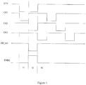
- Fig.4 is a view illustrating an operation timing of the light-emitting control circuit according to the second embodiment of the present disclosure, wherein the light-emitting control circuit is the first light-emitting control circuit stage in the shift register.
- a pulse width of the STV is twice as a pulse width of the CK1, a pulse width of the CK2 and a pulse width of the CK3.
- a first falling edge of the CK1 aligns with a falling edge of the STV; a first falling edge of the CK2 aligns with a first rising edge of the CK2; a first falling edge of the CK3 aligns with a rising edge of the STV; a duty ratios of the CK1, the CK2 and the CK3 are 1/3.
- a t1 stage is an input sampling stage.
- the input signal STV is also in the low level, and the CK1 is in the low level at this moment so the T1 is turned on, the CK3 is in the high level so the T8 is turned off, then the level at the N1 node is pulled down to VGL+
- the T10 and T11 are turned on, the N2 node and the N3 node are in the high level, and because the transistors T4 and T6 are turned off, the levels at the N3 node and the N5 node are ensured; on the other hand, the T13 is turned on, so the light-emitting control signal output from the outputting terminal EM[n] for the light-emitting control signal is in the low level; wherein Vthp is a threshold voltage of a p-type thin film transistor.
- a t2 stage is an outputting stage.
- the CK1 and CK3 are in the high level, the transistors T1, T3, T2 and T9 are all turned off, the level at the N1 node is pulled down correspondingly because of the bootstrap effect of the capacitor C1; the T3 is turned on, the CK2 signal is in the low level, the level at the N2 node is low at this time, then the T4 is turned on to pull down the level at the N3 node; accordingly, the T6 is turned on, the N5 node is in the high level and the T13 is turned off; the T7 is turned on since the CK2 is in the low level, so the light-emitting control signal output from the outputting terminal EM[n] for the light-emitting control signal is a high level signal and provides a ON signal to the OLED device.
- a t3 stage is a resetting stage.
- the CK3 is low, the T8 and T9 are turned on accordingly to pull up the level at the N1 node and pull down the level at the N4 node.
- the T12 is turned on, the level at the N5 node is in the low level.
- the T10 and T11 are turned on so as to pull up the levels at the N2 node and the N3 node.
- the T4 and T6 are turned off so that the levels at the N3 node and the N5 node are ensured; the T13 is turned on since the N5 node is in the low level, then the light-emitting control signal output from the outputting terminal EM[n] for the light-emitting control signal is pulled down again at this time, thus a resetting of the light-emitting control signal is achieved.
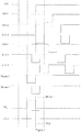
- Fig.5 is a view illustrating an operation timing of the shift register as shown in Fig.3 .
- EM_out_1, EM_out_2, EM_out_n denote an opposite phase outputting terminal of a first light-emitting control circuit stage, an opposite phase outputting terminal of a second light-emitting control circuit stage and an opposite phase outputting terminal of a nth light-emitting control circuit stage, respectively.
- EM_1, EM_2, EM_n denote the light-emitting control signal output from the first light-emitting control circuit stage, light-emitting control signal output from the second light-emitting control circuit stage and the light-emitting control signal output from the nth light-emitting control circuit stage, respectively.
- n is an integer being smaller than or equal to a number of stages of the light-emitting control circuits included in the shift register.
- a pulse width of CLK1-1, a pulse width of CLK1-2, a pulse width of CLK1-3, a pulse width of CLK2-1, a pulse width of CLK2-2 and a pulse width of CLK2-3 are same.
- a pulse width of the start signal STV is twice as the pulse width of CLK1-1, the pulse width of CLK1-2, the pulse width of CLK1-3, the pulse width of CLK2-1, the pulse width of CLK2-2 and the pulse width of CLK2-3, respectively.
- a first falling edge of the CLK1-1 aligns with a falling edge of the STV; a first falling edge of the CLK1-2 aligns with a first rising edge of the CLK1-1; a first falling edge of the CLK1-3 aligns with a rising edge of the STV; a first falling edge of the CLK2-1 locates at a 1/4 pulse width of the STV, that is, at a 1/2 pulse width of the CLK1-1 itself; a first falling edge of the CLK2-2 aligns with a first rising edge of the CLK2-1; a first falling edge of the CLK2-3 aligns with a first rising edge of the CLK2-2; a duty ratio of the CLK1-1, a duty ratio of the CLK1-2, a duty ratio of the CLK1-3, a duty ratio of the CLK2-1, a duty ratio of the CLK2-2 and a duty ratio of the CLK2-3 are 1/3.
- the embodiments of the present disclosure further provide a light-emitting control method for generating a light-emitting control signal which controls an OLED to emit light in an AMOLED, phases of the light-emitting control signal and a gate driving signal are opposite; the light-emitting control method comprises steps of:
- a resetting step in which a resetting unit resets the light-emitting control signal through the output pulling-down unit under a control of a third clock signal.
Description
- The present disclosure relates to a field of organic light-emitting display, and in particular to a light-emitting control circuit, a light-emitting control method and a shift register.
- An Organic Light-Emitting Diode (OLED) has been applied to displays with a high performance more and more because of its advantages such as a high luminance, a wide viewing angle, a rapid response speed and etc. Traditional passive matrix OLED (PMOLED) requires shorter driving time for a single pixel as its display size becomes bigger, therefore an instantaneous current is increased and a power consumption is also increased. Further, an application with a big current would cause a voltage drop on an ITO line too great and an operation voltage at the OLED too high, which may decrease its efficiency in turn. As compared, an active matrix OLED (AMOLED) may solve these problem well by scanning input OLED currents progressively with switching transistors.
- For an AMOLED (Active Matrix Organic Light Emitting Diode) display, not only a row strobing signal for controlling an ON/OFF state of a pixel connected with a gate is required to be generated, but also an ON/OFF state of the organic light emitting diode (OLED) is required to be controlled. A state controlling signal for the OLED is a positive level signal with respect to an AMOLED display backboard composed of p-type transistors, in order to ensure that an OLED device is in the OFF state during a process for writing display data into pixel cells and the OLED device is turned on to emit light after the display data is written into the pixel cells, thereby a display image is guaranteed not to generate flickers due to an unstable state of a pixel circuit as the data is written.
-
CN 102 201 194 A discloses a shift register circuit comprising a multi-stage shift register, wherein each stage of the shift register comprises a first pull-down unit for pulling down scanning signals according to a driving control voltage and a first clock, an input unit for outputting a drive control voltage according to inputted signals and a second clock inverse to the first clock, a first control unit for providing a first control signal according to the drive control voltage, a first pull-up unit for pulling up the drive control voltage and the scanning signals according to the first control signal, a second pull-up unit for pulling up light-emitting signals according to the scanning signals,; a second control unit for providing a second control signal according to the scanning signals and a second pull-down unit for pulling down the light-emitting signals according to the second control signal. -
EP 1 763 003 A1 -
US 2011/193892 A1 discloses a display device including a display unit and a light emission driver. The display unit includes scan lines for transmitting scan signals, data lines for transmitting data signals, light emitting signal lines for transmitting light emitting signals, and pixels coupled to the scan lines, data lines, and light emitting signal lines. The light emission driver is for receiving a partial driving selection signal for selecting one of a normal driving mode or a partial driving mode, an area selection signal for dividing the display unit into a display area and a non-display area, a synchronization signal generated in synchronization with a vertical synchronization signal, and first and second light emitting clock signals, for outputting the light emitting signals. - A major object of the present invention is to provide a light-emitting control circuit, a light-emitting control method and a shift register, which may be capable of ensuring that an OLED device is in an OFF state during a process for writing display data into pixel cells and the OLED device is turned on to emit light after the display data is written into the pixel cells, thus a display image is guaranteed not to generate flickers due to a unstable state of a pixel circuit as the data is written.
- The object is achieved by the features of the independent claims. Further embodiments are defined in the respective dependent claims.
- In order to achieve the above objects, the embodiments of the present disclosure provide a light-emitting control circuit for generating a light-emitting control signal which controls an OLED to emit light in an AMOLED, phases of the light-emitting control signal and a gate driving signal are opposite;
the light-emitting control circuit comprises an inputting terminal, an input sampling unit, an outputting unit, a resetting unit, an output pulling-down unit and an outputting terminal for a light-emitting control signal, wherein,
the output pulling-down unit is connected with the outputting terminal for the light-emitting control signal;
the input sampling unit is connected with the inputting terminal, a first clock signal inputting terminal and the output pulling-down unit, respectively, and is used for sampling an input signal under a control of a first clock signal and transmitting the sampled signal to the outputting terminal for the light-emitting control signal through the output pulling-down unit;
the outputting unit is connected with the input sampling unit, a second clock signal inputting terminal and the outputting terminal for the light-emitting control signal, respectively, and is used for generating a light-emitting control signal under a control of a second clock signal after the input sampling unit samples the input signal and transmitting the light-emitting control signal to the outputting terminal for the light-emitting control signal;
the resetting unit is connected with a third clock signal inputting terminal and the output pulling-down unit, respectively, and is used for sending a resetting control signal to the output pulling-down unit under a control of a third clock signal;
the output pulling-down unit is used for resetting the light-emitting control signal according to the resetting control signal. - According to the embodiments of the present disclosure, the input sampling unit comprises a first thin film transistor and a second thin film transistor;
a gate of the first thin film transistor is connected with the first clock signal inputting terminal, a source thereof is connected with the outputting unit, and a drain thereof is connected with the inputting terminal;
a gate of the second thin film transistor is connected with the first clock signal inputting terminal, a source thereof is connected with the outputting unit, and a drain thereof is connected with a low level outputting terminal of a driving power supply;
the outputting unit comprises a third thin film transistor, a fourth thin film transistor, a fifth thin film transistor, a sixth thin film transistor, a seventh thin film transistor, a first capacitor and a second capacitor;
a gate of the third thin film transistor is connected with the source of the first thin film transistor, a source thereof is connected with a gate of the fourth thin film transistor, and a drain thereof is connected with the second clock signal inputting terminal;
the gate of the fourth thin film transistor is connected with the source of the third thin film transistor, a source thereof is connected with a gate of the sixth thin film transistor, and a drain thereof is connected with the low level outputting terminal of the driving power supply;
a gate of the fifth thin film transistor is connected with the second clock signal inputting terminal, a source thereof is connected with a high level outputting terminal of the driving power supply, and a drain thereof is connected with the source of the second thin film transistor;
the source of the sixth thin film transistor is connected with the high level outputting terminal of the driving power supply, and a drain thereof is connected with a source of a twelfth thin film transistor;
a gate of the seventh thin film transistor is connected with the second clock signal inputting terminal, a source thereof is connected with the high level outputting terminal of the driving power supply, and a drain thereof is connected with a source of a thirteenth thin film transistor;
the first capacitor is connected between the gate and source of the third thin film transistor;
the second capacitor is connected between the gate of the sixth thin film transistor and the low level outputting terminal of the driving power supply;
the resetting unit comprises an eighth thin film transistor and a ninth thin film transistor;
a gate of the eighth thin film transistor is connected with the third clock signal inputting terminal, a source thereof is connected with the high level outputting terminal of the driving power supply, and a drain thereof is connected with the source of the first thin film transistor;
a gate of the ninth thin film transistor is connected with the third clock signal inputting terminal, a source thereof is connected with the source of the second thin film transistor, and a drain thereof is connected with the low level outputting terminal of the driving power supply. - According to the embodiments of the present disclosure, the output pulling-down unit comprises a tenth thin film transistor, an eleventh thin film transistor, the twelfth thin film transistor, the thirteenth thin film transistor, a third capacitor, a fourth capacitor, a fifth capacitor and a sixth capacitor;
a gate of the tenth thin film transistor is connected with a gate of the eleventh thin film transistor, a source thereof is connected with the high level outputting terminal of the driving power supply, and a drain thereof is connected with the source of the third thin film transistor;
a source of the eleventh thin film transistor is connected with the high level outputting terminal of the driving power supply, and a drain thereof is connected with the source of the fourth thin film transistor;
a gate of the twelfth thin film transistor is connected with the source of the second thin film transistor, the source thereof is connected with the drain of the sixth thin film transistor, and a drain thereof is connected with the low level outputting terminal of the driving power supply;
a gate of the thirteenth thin film transistor is connected with the gate of the tenth thin film transistor, a source thereof is connected with the outputting terminal for the light-emitting control signal, and a drain thereof is connected with the low level outputting terminal of the driving power supply;
the third capacitor is connected between the gate and source of the twelfth thin film transistor;
the fourth capacitor is connected the gate and source of the thirteenth thin film transistor;
the fifth capacitor is connected between the gate of the tenth thin film transistor and the low level outputting terminal of the driving power supply;
the sixth capacitor is connected between the outputting terminal for the light-emitting control signal and the low level outputting terminal of the driving power supply. - The light-emitting control circuit according to the embodiments of the present disclosure further comprises an opposite phase outputting terminal;
the gate of the forth thin film transistor is connected with the opposite phase outputting terminal,;
a signal output from the opposite phase outputting terminal has an opposite phase to the light-emitting control signal. - According to the embodiments of the present disclosure, the first thin film transistor, the second thin film transistor, the third thin film transistor, the fourth thin film transistor, the fifth thin film transistor, the sixth thin film transistor, the seventh thin film transistor, the eighth thin film transistor, the ninth thin film transistor, the tenth thin film transistor, the eleventh thin film transistor, the twelfth thin film transistor and the thirteenth thin film transistor are p-type TFTs.
- The embodiments of the present disclosure further provide a light-emitting control method applied to the light-emitting control circuit, for generating a light-emitting control signal which controls an OLED to emit light in an AMOLED, phases of the light-emitting control signal and a gate driving signal is opposite;
the light-emitting control method comprises steps of: - an input sampling step in which a input sampling unit samples an input signal under a control of a first clock signal and transmits the sampled signal to a outputting terminal for the light-emitting control signal through the output pulling-down unit;
- an outputting step in which an outputting unit generates a light-emitting control signal under a control of a second clock signal after the input sampling unit samples the input signal and transmitting the light-emitting control signal to the outputting terminal for the light-emitting control signal;
- a resetting step in which a resetting unit resets the light-emitting control signal through the output pulling-down unit under a control of a third clock signal.
- The embodiments of the present disclosure further provide a shift register comprising a plurality of light-emitting control circuit stages described above;
except for the first light-emitting control circuit stage and the second light-emitting control circuit stage, an input signal of the nth light-emitting control circuit stage is a signal having an phase opposite to a light-emitting control signal from a (n-2)th light-emitting control circuit stage;
an input signal of the first light-emitting control circuit stage and an input signal of the second light-emitting control circuit stage are a start signal;
n is an integer being greater than 2 and smaller than or equal to N, the N is a number of stages of the light-emitting control circuits included in the shift register. - As compared with the prior art, the light-emitting control circuit, the light-emitting control method and the shift register according to the embodiments of the present disclosure generate the light-emitting control signal having the phase opposite to that of the gate driving signal, so that the OLED device is in the OFF state during the process for writing display data into pixel cells and the OLED device is turned on to light after the display data is written into the pixel cells, thus a display image is guaranteed not to generate flickers due to an unstable state of a pixel circuit as the data is written.
-
-
Fig.1 is a circuit diagram illustrating a light-emitting control circuit according to a first embodiment of the present disclosure; -
Fig.2 is a circuit diagram illustrating a light-emitting control circuit according to a second embodiment of the present disclosure; -
Fig.3 is a circuit diagram illustrating a shift register according to an embodiment of the present disclosure; -
Fig.4 is a view illustrating an operation timing of the light-emitting control circuit according to the second embodiment of the present disclosure; and -
Fig.5 is a view illustrating an operation timing of the shift register as shown inFig.3 . - Objects, solutions and advantages of the present disclosure will be more apparent from the following detailed description for the embodiments of the present disclosure taken in conjunction with the accompanying drawings. Herein, the exemplary embodiments of the present disclosure and their description aim to only illustrate the present disclosure but not to limit the present disclosure.
- For an Active Matrix Liquid Crystal Display (AMLCD), a gate driving circuit is used for generating a row strobing control signal for a pixel circuit array. However, for an Active Matrix Organic Light Emitting Diode (AMOLED) display, an OLED is a device driven by a current, therefore a light emitting of an OLED device may be controlled by control a path through which the current flows into the OLED. Thus, the embodiments of the present disclosure provide a light-emitting control circuit, a light-emitting control method and a shift register in order to control the light emitting of the OLED in the AMOLED display accurately.
- The light-emitting control circuit according to the embodiments of the present disclosure cooperates with a conventional gate driving circuit, and may achieve respective controls to operation states of the OLED and the pixel circuit.
- As illustrated in
Fig.1 , a light-emitting control circuit according to a first embodiment of the present disclosure is used for generating a light-emitting control signal which controls an OLED to emit light in an AMOLED, phases of the light-emitting control signal and a gate driving signal are opposite;
the light-emitting control circuit comprises an inputting terminal INPUT, aninput sampling unit 11, an outputtingunit 12, a resettingunit 13, an output pulling-downunit 14 and an outputting terminal EM[n] for a light-emitting control signal, wherein,
theinput sampling unit 11 is connected with the inputting terminal INPUT, the outputtingunit 12, a first clock signal inputting terminal and the output pulling-downunit 14, respectively, and is used for sampling an input signal under a control of a first clock signal and transmitting the sampled signal to the outputting terminal EM[n] for the light-emitting control signal through the output pulling-downunit 14;
the outputtingunit 12 is connected with theinput sampling unit 11, a second clock signal inputting terminal and the outputting terminal EM[n] for the light-emitting control signal, respectively, and is used for generating a light-emitting control signal under a control of a second clock signal after theinput sampling unit 11 samples the input signal and transmitting the light-emitting control signal to the outputting terminal EM[n] for the light-emitting control signal;
the resettingunit 13 is connected with a third clock signal inputting terminal and the output pulling-downunit 14, respectively, and is used for sending a resetting control signal to the output pulling-down unit under a control of a third clock signal;
the output pulling-downunit 14 is connected with the outputting terminal EM[n] for the light-emitting control signal, and is used for resetting the light-emitting control signal under a control of the resetting control signal;
the first clock signal CK1 is input from the first clock signal inputting terminal, the second clock signal CK2 is input from the second clock signal inputting terminal, and the third clock signal CK3 is input from the third clock signal inputting terminal. - The light-emitting control circuit according to the first embodiment of the present disclosure may generate the light-emitting control signal which controls the OLED to emit light in the AMOLED, wherein the light-emitting control signal has an opposite phase to that of the gate driving signal. Such light-emitting control circuit may control the light-emitting of the OLED accurately in the AMOLED display, so that the OLED device is in an OFF state during a process for writing display data into pixel cells and the OLED device is turned on to emit light after the display data is written into the pixel cells, thus a display image is guaranteed not to generate flickers due to an unstable state of a pixel circuit as the data is written.
-
Fig.2 is a circuit diagram illustrating a light-emitting control circuit according to a second embodiment of the present disclosure. As illustrated inFig.2 , the light-emitting control circuit according to the second embodiment of the present disclosure is based on the light-emitting control circuit according to the first embodiment of the present disclosure. In the light-emitting control circuit according to the second embodiment of the present disclosure: - the input sampling unit comprises a first thin film transistor T1 and a second thin film transistor T2;
- the outputting unit comprises a third thin film transistor T3, a fourth thin film transistor T4, a fifth thin film transistor T5, a sixth thin film transistor T6, a seventh thin film transistor T7, a first capacitor C1 and a second capacitor C2;
- the resetting unit comprises an eighth thin film transistor T8 and a ninth thin film transistor T9;
- the output pulling-down unit comprises a tenth thin film transistor T10, an eleventh thin film transistor T11, the twelfth thin film transistor T12, the thirteenth thin film transistor T13, a third capacitor C3, a fourth capacitor C4, a fifth capacitor C5 and a sixth capacitor C6;
- a gate of the first thin film transistor T1 is connected with the first clock signal inputting terminal, a source thereof is connected with a gate of the third thin film transistor T3, and a drain thereof is connected with the inputting terminal INPUT;
- a gate of the second thin film transistor T2 is connected with the first clock signal inputting terminal, a source thereof is connected with a drain of the fifth thin film transistor T5, and a drain thereof is connected with a low level outputting terminal of a driving power supply;
- a source of the third thin film transistor T3 is connected with a gate of the fourth thin film transistor T4, and a drain thereof is connected with the second clock signal inputting terminal;
- a source of the fourth thin film transistor T4 is connected with a gate of the sixth thin film transistor T6, and a drain thereof is connected with the low level outputting terminal of the driving power supply;
- a gate of the fifth thin film transistor T5 is connected with the second clock signal inputting terminal, and a source thereof is connected with a high level outputting terminal of the driving power supply;
- the source of the sixth thin film transistor T6 is connected with the high level outputting terminal of the driving power supply, and a drain thereof is connected with a source of the twelfth thin film transistor T12;
- a gate of the seventh thin film transistor T7 is connected with the second clock signal inputting terminal, a source thereof is connected with the high level outputting terminal of the driving power supply, and a drain thereof is connected with a source of the thirteenth thin film transistor T13;
- a gate of the eighth thin film transistor T8 is connected with the third clock signal inputting terminal, a source thereof is connected with the high level outputting terminal of the driving power supply, and a drain thereof is connected with the source of the first thin film transistor T1;
- a gate of the ninth thin film transistor T9 is connected with the third clock signal inputting terminal, a source thereof is connected with the source of the second thin film transistor T2, and a drain thereof is connected with the low level outputting terminal of the driving power supply;
- a gate of the tenth thin film transistor T10 is connected with a gate of the eleventh thin film transistor T11, a source thereof is connected with the high level outputting terminal of the driving power supply, and a drain thereof is connected with the source of the third thin film transistor T3;
- a source of the eleventh thin film transistor T11 is connected with the high level outputting terminal of the driving power supply, and a drain thereof is connected with the source of the fourth thin film transistor T4;
- a gate of the twelfth thin film transistor T12 is connected with the source of the second thin film transistor T2, the source thereof is connected with the drain of the sixth thin film transistor T6, and a drain thereof is connected with the low level outputting terminal of the driving power supply;
- a gate of the thirteenth thin film transistor T13 is connected with the gate of the tenth thin film transistor T10, a source thereof is connected with the outputting terminal EM[n] for the light-emitting control signal, and a drain thereof is connected with the low level outputting terminal of the driving power supply;
- the first capacitor C1 is connected between the gate and source of the third thin film transistor T3;
- the second capacitor C2 is connected between the gate of the sixth thin film transistor T6 and the low level outputting terminal of the driving power supply
- the third capacitor C3 is connected between the gate and source of the twelfth thin film transistor T12;
- the fourth capacitor C4 is connected the gate and source of the thirteenth thin film transistor T13;
- the fifth capacitor C5 is connected between the gate of the tenth thin film transistor T10 and the low level outputting terminal of the driving power supply;
- the sixth capacitor C6 is connected between the outputting terminal EM[n] for the light-emitting control signal and the low level outputting terminal of the driving power supply;
- the first clock signal CK1 is input from the first clock signal inputting terminal, the second clock signal CK2 is input from the second clock signal inputting terminal, and the third clock signal CK3 is input from the third clock signal inputting terminal;
- an output voltage from the high level outputting terminal of the driving power supply is VGH, and an output voltage from the low level outputting terminal of the driving power supply is VGL;
- a N1 node is a node with which the gate of the third thin film transistor T3 is connected;
- a N2 node is a node with which the gate of the fourth thin film transistor T4 is connected;
- a N3 node is a node with which the gate of the sixth thin film transistor T6 is connected;
- a N4 node is a node with which the gate of the twelfth thin film transistor T12 is connected;
- a N5 node is a node with which the gate of the thirteenth thin film transistor T13 is connected;
- the N2 node (that is, an opposite phase outputting terminal EM_out) is connected with the next shift register unit stage in order to provide an input signal for the next shift register unit stage;
- a signal output from the opposite phase outputting terminal EM_out has an opposite phase to that of a light-emitting control signal;
- wherein the C1, C3 and C4 are bootstrap capacitors, the C2, C4 and C6 are storage capacitors; the bootstrap capacitor is mostly used to pull up or pull down a level at a node, while the storage capacitor is mostly used to remain the level at the node.
- The first thin film transistor T1, the second thin film transistor T1, the third thin film transistor T3, the fourth thin film transistor T4, the fifth thin film transistor T5, the sixth thin film transistor T6, the seventh thin film transistor T7, the eighth thin film transistor T8, the ninth thin film transistor T9, the tenth thin film transistor T10, the eleventh thin film transistor T11, the twelfth thin film transistor T12 and the thirteenth thin film transistor T13 are p-type TFTs.
- As illustrated in
Fig.3 , a shift register according to an embodiment of the present disclosure comprises a plurality of the light-emitting control circuit stages according to the second embodiment of the present disclosure;
except for the first light-emitting control circuit stage and the second light-emitting control circuit stage, an inputting terminal Input of the nth light-emitting control circuit stage is connected with an opposite phase outputting terminal EM_out of a (n-2)th light-emitting control circuit stage;
an inputting terminal Input of the first light-emitting control circuit stage and an inputting terminal Input of the second light-emitting control circuit stage are connected with a start signal inputting terminal;
a start signal STV is input from the start signal inputting terminal;
n is an integer being greater than 2 and smaller than or equal to N, the N is a number of stages of the light-emitting control circuits included in the shift register. - In
Fig.3 , STAGE_1, STAGE_2, STAGE_3, STAG_4, STAGE_5, STAGE_6, STAGE_7 and STAGE_8 denote the first light-emitting control circuit stage, the second light-emitting control circuit stage, the third light-emitting control circuit, the fourth light-emitting control circuit stage, the fifth light-emitting control circuit stage, the sixth light-emitting control circuit stage, the seventh light-emitting control circuit and the eighth light-emitting control circuit stage, respectively. - Also, the first clock signal, the second clock signal and the third clock signal connected with an odd light-emitting control circuit stage are CLK1-1, CLK1-2 and CLK1-3, respectively;
the first clock signal, the second clock signal and the third clock signal connected with an even light-emitting control circuit stage are CLK2-1, CLK2-2 and CLK2-3, respectively. -
Fig.4 is a view illustrating an operation timing of the light-emitting control circuit according to the second embodiment of the present disclosure, wherein the light-emitting control circuit is the first light-emitting control circuit stage in the shift register. - A pulse width of the STV is twice as a pulse width of the CK1, a pulse width of the CK2 and a pulse width of the CK3.
- A first falling edge of the CK1 aligns with a falling edge of the STV;
a first falling edge of the CK2 aligns with a first rising edge of the CK2;
a first falling edge of the CK3 aligns with a rising edge of the STV;
a duty ratios of the CK1, the CK2 and the CK3 are 1/3. - As illustrated in
Fig.4 , a t1 stage is an input sampling stage. At this time, the input signal STV is also in the low level, and the CK1 is in the low level at this moment so the T1 is turned on, the CK3 is in the high level so the T8 is turned off, then the level at the N1 node is pulled down to VGL+|Vthp|; at the same time, the T2 is turned on because the CK1 is in the low level, the N4 node is in the low level, the T12 is turned on, the N5 node is in the low level. Thus, on the one hand, the T10 and T11 are turned on, the N2 node and the N3 node are in the high level, and because the transistors T4 and T6 are turned off, the levels at the N3 node and the N5 node are ensured; on the other hand, the T13 is turned on, so the light-emitting control signal output from the outputting terminal EM[n] for the light-emitting control signal is in the low level; wherein Vthp is a threshold voltage of a p-type thin film transistor. - A t2 stage is an outputting stage. The CK1 and CK3 are in the high level, the transistors T1, T3, T2 and T9 are all turned off, the level at the N1 node is pulled down correspondingly because of the bootstrap effect of the capacitor C1; the T3 is turned on, the CK2 signal is in the low level, the level at the N2 node is low at this time, then the T4 is turned on to pull down the level at the N3 node; accordingly, the T6 is turned on, the N5 node is in the high level and the T13 is turned off; the T7 is turned on since the CK2 is in the low level, so the light-emitting control signal output from the outputting terminal EM[n] for the light-emitting control signal is a high level signal and provides a ON signal to the OLED device.
- A t3 stage is a resetting stage. The CK3 is low, the T8 and T9 are turned on accordingly to pull up the level at the N1 node and pull down the level at the N4 node. At this time, the T12 is turned on, the level at the N5 node is in the low level. At this moment, the T10 and T11 are turned on so as to pull up the levels at the N2 node and the N3 node. The T4 and T6 are turned off so that the levels at the N3 node and the N5 node are ensured; the T13 is turned on since the N5 node is in the low level, then the light-emitting control signal output from the outputting terminal EM[n] for the light-emitting control signal is pulled down again at this time, thus a resetting of the light-emitting control signal is achieved.
-
Fig.5 is a view illustrating an operation timing of the shift register as shown inFig.3 . InFig.5 , EM_out_1, EM_out_2, EM_out_n denote an opposite phase outputting terminal of a first light-emitting control circuit stage, an opposite phase outputting terminal of a second light-emitting control circuit stage and an opposite phase outputting terminal of a nth light-emitting control circuit stage, respectively. - EM_1, EM_2, EM_n denote the light-emitting control signal output from the first light-emitting control circuit stage, light-emitting control signal output from the second light-emitting control circuit stage and the light-emitting control signal output from the nth light-emitting control circuit stage, respectively.
- Wherein n is an integer being smaller than or equal to a number of stages of the light-emitting control circuits included in the shift register.
- A pulse width of CLK1-1, a pulse width of CLK1-2, a pulse width of CLK1-3, a pulse width of CLK2-1, a pulse width of CLK2-2 and a pulse width of CLK2-3 are same.
- A pulse width of the start signal STV is twice as the pulse width of CLK1-1, the pulse width of CLK1-2, the pulse width of CLK1-3, the pulse width of CLK2-1, the pulse width of CLK2-2 and the pulse width of CLK2-3, respectively.
- A first falling edge of the CLK1-1 aligns with a falling edge of the STV;
a first falling edge of the CLK1-2 aligns with a first rising edge of the CLK1-1;
a first falling edge of the CLK1-3 aligns with a rising edge of the STV;
a first falling edge of the CLK2-1 locates at a 1/4 pulse width of the STV, that is, at a 1/2 pulse width of the CLK1-1 itself;
a first falling edge of the CLK2-2 aligns with a first rising edge of the CLK2-1;
a first falling edge of the CLK2-3 aligns with a first rising edge of the CLK2-2;
a duty ratio of the CLK1-1, a duty ratio of the CLK1-2, a duty ratio of the CLK1-3, a duty ratio of the CLK2-1, a duty ratio of the CLK2-2 and a duty ratio of the CLK2-3 are 1/3. - The embodiments of the present disclosure further provide a light-emitting control method for generating a light-emitting control signal which controls an OLED to emit light in an AMOLED, phases of the light-emitting control signal and a gate driving signal are opposite;
the light-emitting control method comprises steps of: - an input sampling step in which an input sampling unit samples an input signal under a control of a first clock signal and transmits the sampled signal to an outputting terminal for the light-emitting control signal through the output pulling-down unit;
- an outputting step in which an outputting unit generates a light-emitting control signal under a control of a second clock signal after the input sampling unit samples the input signal and transmitting the light-emitting control signal to the outputting terminal for the light-emitting control signal; the light-emitting control signal is the turning on signal driving the TFT provided to the OLED device.
- a resetting step in which a resetting unit resets the light-emitting control signal through the output pulling-down unit under a control of a third clock signal.
Claims (7)
- A system comprising a gate driving circuit adapted to output a gate driving signal and a light-emitting control circuit adapted to generate a light-emitting control signal for controlling an organic light emitting diode, OLED, to emit light in an active matrix OLED, AMOLED, the light-emitting control circuit being adapted to output a light-emitting control signal having a phase opposite to the phase of the gate driving signal, the light-emitting control circuit being adapted to be connected to a low level outputting terminal (VGL) and a high level outputting terminal (VGH) of a driving power supply;
the light-emitting control circuit comprises an inputting terminal (Input), an input sampling unit (11), an outputting unit (12), a resetting unit (13), an output pulling-down unit (14) and a outputting terminal (EM[n]) for the light-emitting control signal, wherein,
the output pulling-down unit (14) is connected with the outputting terminal (EM[n]);
the input sampling unit (11) is connected with the inputting terminal (Input), a first clock signal inputting terminal (CK1) and the output pulling-down unit (14), respectively, and is adapted to sample an input signal received on the inputting terminal (Input) under control of a first clock signal received on the first clock signal inputting terminal (CK1) and to transmit the sampled signal to the outputting terminal (EM[n]) for the light-emitting control signal through the output pulling-down unit (14);
the outputting unit (12) is connected with the input sampling unit (11), a second clock signal inputting terminal (CK2) and the outputting terminal (EM[n]), respectively, and is adapted to generate the light-emitting control signal under control of a second clock signal received on the second clock signal inputting terminal (CK2) after the input sampling unit (11) samples the input signal and to transmit the light-emitting control signal to the outputting terminal (EM[n]) for the light-emitting control signal;
the resetting unit (13) is connected with a third clock signal inputting terminal (CK3) and the output pulling-down unit (14), respectively, and is adapted to send a resetting control signal to the output pulling-down unit (14) under control of a third clock signal received on the third clock signal inputting terminal (CK3);
the output pulling-down unit (14) is adapted to reset the light-emitting control signal according to the resetting control signal;
the input sampling unit (11) comprises a first thin film transistor (T1) and a second thin film transistor (T2);
a gate of the first thin film transistor (T1) is connected with the first clock signal (CK1) inputting terminal, a source thereof is connected with the outputting unit (12), and a drain thereof is connected with the inputting terminal (Input);
a gate of the second thin film transistor (T2) is connected with the first clock signal inputting terminal (CK1), a source thereof is connected with the outputting unit (12), and a drain thereof is connected with the low level outputting terminal (VGL) of the driving power supply;
the output pulling-down unit (14) comprises a twelfth thin film transistor (T12), a gate thereof is connected with the source of the second thin film transistor (T2), a drain thereof is connected with the low level outputting terminal (VGL) of the driving power supply;
the outputting unit (12) comprises a third thin film transistor (T3), a fourth thin film transistor (T4), a fifth thin film transistor (T5), a sixth thin film transistor (T6), a first capacitor (C1) and a second capacitor (C2);
a gate of the third thin film transistor (T3) is connected with the source of the first thin film transistor (T1), a source thereof is connected with a gate of the fourth thin film transistor (T4), and a drain thereof is connected with the second clock signal inputting terminal (CK2);
a source of the fourth thin film transistor (T4) is connected with a gate of the sixth thin film transistor (T6), and a drain thereof is connected with the low level outputting terminal (VGL) of the driving power supply;
a source of the fifth thin film transistor (T5) is connected with the high level outputting terminal (VGH) of the driving power supply, and a drain thereof is connected with the source of the second thin film transistor (T2);
the source of the sixth thin film transistor (T6) is connected with the high level outputting terminal (VGH) of the driving power supply, and a drain thereof is connected with a source of the twelfth thin film transistor (T12);the first capacitor (C1) is connected between the gate and source of the third thin film transistor (T3);the system being characterized in that:- the output pulling-down unit (14) further comprises a thirteenth thin film transistor (T13) and a fourth capacitor (C4), wherein a source of the thirteenth thin film transistor (T13) is connected with the outputting terminal (EM[n]), a gate thereof is connected to the source of the twelfth thin film transistor (T12) and a drain thereof is connected with the low level outputting terminal (VGL) of the driving power supply, and wherein the fourth capacitor (C4) is connected the gate and source of the thirteenth thin film transistor (T13); and- the outputting unit (12) further comprises a second capacitor (C2) and a seventh thin film transistor (T7), wherein a gate thereof is connected with the second clock signal inputting terminal (CK2), a source thereof is connected with the high level outputting terminal (VGH) of the driving power supply, and a drain thereof is connected with a source of a thirteen thin film transistor (T13), and wherein a gate of the fifth thin film transistor (T5) is connected with the second clock signal inputting terminal (CK2), and wherein the second capacitor (C2) is connected between the gate of the sixth thin film transistor (T6) and the low level outputting terminal (VGL) of the driving power supply. - The system of claim 1, wherein,
the resetting unit (13) comprises an eighth thin film transistor (T8) and a ninth thin film transistor (T9);
a gate of the eighth thin film transistor (T8) is connected with the third clock signal inputting terminal (CK3), a source thereof is connected with the high level outputting terminal (VGH) of the driving power supply, and a drain thereof is connected with the source of the first thin film transistor (T1);
a gate of the ninth thin film transistor (T9) is connected with the third clock signal (CK3) inputting terminal, a source thereof is connected with the source of the second thin film transistor (T2), and a drain thereof is connected with the low level outputting terminal (VGL) of the driving power supply. - The system of claim 2, wherein,
the output pulling-down unit (14) further comprises a tenth thin film transistor (T10), an eleventh thin film transistor (T11), a third capacitor (C3), a fifth capacitor (C5) and a sixth capacitor (C6);
a gate of the tenth thin film transistor (T10) is connected with a gate of the eleventh thin film transistor (T11), a source thereof is connected with the high level outputting terminal (VGH) of the driving power supply, and a drain thereof is connected with the source of the third thin film transistor (T3);
a source of the eleventh thin film transistor (T11) is connected with the high level outputting terminal (VGH) of the driving power supply, and a drain thereof is connected with the source of the fourth thin film transistor (T4); a gate of the thirteenth thin film transistor (T13) is connected with the gate of the tenth thin film transistor (T10),;
the third capacitor (C3) is connected between the gate and source of the twelfth thin film transistor (T12);
the fifth capacitor (C5) is connected between the gate of the tenth thin film transistor (T10) and the low level outputting terminal (VGL) of the driving power supply;
the sixth capacitor (C6) is connected between the outputting terminal (EM[n]) and the low level outputting terminal (VGL) of the driving power supply. - The system of claim 3, wherein,
the light-emitting control circuit further comprises an opposite phase outputting terminal (EM_out);
the gate of the fourth thin film transistor (T4) is connected with the opposite phase outputting terminal (EM_out);
a signal output from the opposite phase outputting terminal (EM_out) has an opposite phase to that of the light-emitting control signal. - The system of claim 3 or 4, wherein the first thin film transistor (T1), the second thin film transistor (T2), the third thin film transistor (T3), the fourth thin film transistor (T4), the fifth thin film transistor (T5), the sixth thin film transistor (T6), the seventh thin film transistor (T7), the eighth thin film transistor (T8), the ninth thin film transistor (T9), the tenth thin film transistor (T10), the eleventh thin film transistor (T11), the twelfth thin film transistor (T12) and the thirteenth thin film transistor (T13) are p-type TFTs.
- A light-emitting control method for controlling the system of any one of claims 1-5, for generating the light-emitting control signal for controlling an organic light emitting diode, OLED, to emit light in an active matrix OLED, AMOLED, wherein the phase of the light-emitting control signal is opposite to the phase of the gate driving signal outputted by the gate driving circuit;
the light-emitting control method comprises steps of:an input sampling step in which the input sampling unit (11) samples the input signal under control of a first clock signal (CK1) and transmits the sampled signal to the outputting terminal (EM[n]) for the light-emitting control signal through the output pulling-down unit (14);an outputting step in which the outputting unit (12) generates the light-emitting control signal under control of a second clock (CK2) signal after the input sampling unit (11) samples the input signal and transmits the light-emitting control signal to the outputting terminal (EM[n]) for the light-emitting control signal;a resetting step in which the resetting unit (13) resets the light-emitting control signal through the output pulling-down unit (14) under control of the third clock signal (CK3). - A system according to any of claims 1-5 further comprising a shift register comprising a plurality of light-emitting control circuit, wherein,
except for the first light-emitting control circuit stage (STAGE_1) and the second light-emitting control circuit stage (STAGE_2), an input signal (Input) of the nth light-emitting control circuit stage (STAGE_3, STAG_4, STAGE_5, STAGE_6, ...) is a signal having an phase opposite to that of a light-emitting control signal from a (n-2)th light-emitting control circuit stage;
an input signal of the first light-emitting control circuit stage (STAGE_1) and an input signal of the second light-emitting control circuit stage (STAGE_2) are a start signal (STV);
n is an integer being greater than 2 and smaller than or equal to N, the N is a number of stages of the light-emitting control circuits included in the shift register.
Applications Claiming Priority (2)
| Application Number | Priority Date | Filing Date | Title |
|---|---|---|---|
| CN201210244368.3A CN102760406B (en) | 2012-07-13 | 2012-07-13 | Light-emitting control circuit, light-emitting control method and shift register |
| PCT/CN2012/084973 WO2014008732A1 (en) | 2012-07-13 | 2012-11-21 | Light-emitting control circuit, light-emitting control method and shift register |
Publications (3)
| Publication Number | Publication Date |
|---|---|
| EP2874140A1 EP2874140A1 (en) | 2015-05-20 |
| EP2874140A4 EP2874140A4 (en) | 2016-03-09 |
| EP2874140B1 true EP2874140B1 (en) | 2018-04-04 |
Family
ID=47054853
Family Applications (1)
| Application Number | Title | Priority Date | Filing Date |
|---|---|---|---|
| EP12880722.9A Active EP2874140B1 (en) | 2012-07-13 | 2012-11-21 | Light-emitting control circuit, light-emitting control method and shift register |
Country Status (4)
| Country | Link |
|---|---|
| US (1) | US9113534B2 (en) |
| EP (1) | EP2874140B1 (en) |
| CN (1) | CN102760406B (en) |
| WO (1) | WO2014008732A1 (en) |
Cited By (1)
| Publication number | Priority date | Publication date | Assignee | Title |
|---|---|---|---|---|
| US11151946B2 (en) | 2019-01-04 | 2021-10-19 | Boe Technology Group Co., Ltd. | Shift register unit and driving method, gate driving circuit, and display device |
Families Citing this family (27)
| Publication number | Priority date | Publication date | Assignee | Title |
|---|---|---|---|---|
| CN102760406B (en) | 2012-07-13 | 2015-01-28 | 京东方科技集团股份有限公司 | Light-emitting control circuit, light-emitting control method and shift register |
| CN102760407B (en) * | 2012-07-13 | 2015-11-25 | 京东方科技集团股份有限公司 | Emission control circuit, light-emitting control method and shift register |
| CN103065584B (en) * | 2012-12-18 | 2015-06-03 | 华南理工大学 | Power source organic electroluminescence scanning drive device and drive method thereof |
| CN103886910B (en) * | 2012-12-19 | 2017-07-11 | 群康科技(深圳)有限公司 | Shift registor |
| TWI595472B (en) | 2014-06-23 | 2017-08-11 | 友達光電股份有限公司 | Display panel |
| CN104157236B (en) * | 2014-07-16 | 2016-05-11 | 京东方科技集团股份有限公司 | A kind of shift register and gate driver circuit |
| TWI546786B (en) * | 2014-08-22 | 2016-08-21 | 友達光電股份有限公司 | Display panel |
| CN104821148B (en) * | 2015-05-28 | 2016-11-09 | 京东方科技集团股份有限公司 | Shift register cell, driving method, gate driver circuit and display device |
| CN104821153B (en) * | 2015-05-29 | 2017-06-16 | 京东方科技集团股份有限公司 | Gate driving circuit and OLED display |
| KR102413874B1 (en) * | 2015-07-02 | 2022-06-29 | 삼성디스플레이 주식회사 | Emissioin driver and display device including the same |
| CN105632560B (en) * | 2016-01-04 | 2019-08-02 | 京东方科技集团股份有限公司 | Shift register cell, driving method, gate driving circuit and display device |
| CN105609054B (en) * | 2016-02-29 | 2018-05-08 | 信利(惠州)智能显示有限公司 | A kind of emission control circuit and shift register |
| CN105632410B (en) * | 2016-03-15 | 2018-04-10 | 上海天马有机发光显示技术有限公司 | A kind of shift register, gate driving circuit, display panel and driving method |
| US10492257B2 (en) * | 2016-05-20 | 2019-11-26 | Panasonic Intellectual Property Management Co., Ltd. | Lighting device and lighting fixture |
| CN108417183B (en) * | 2017-02-10 | 2020-07-03 | 京东方科技集团股份有限公司 | Shift register and driving method thereof, gate drive circuit and display device |
| CN108665853B (en) * | 2017-03-27 | 2020-11-13 | 昆山工研院新型平板显示技术中心有限公司 | Control signal driving circuit and driving method and pixel circuit driving method |
| CN108806588B (en) * | 2017-04-28 | 2020-06-12 | 昆山国显光电有限公司 | Light-emitting control circuit, light-emitting control method and shift register |
| CN107093393A (en) * | 2017-07-03 | 2017-08-25 | 成都晶砂科技有限公司 | The drive circuit that gate driving circuit and light emitting control drive circuit are blended |
| CN108039150B (en) * | 2017-11-16 | 2020-05-19 | 武汉华星光电半导体显示技术有限公司 | Shift register circuit and shift register unit |
| CN108806583B (en) * | 2018-07-05 | 2020-12-01 | 京东方科技集团股份有限公司 | Shift register unit, driving method, shift register and display device |
| CN108682398B (en) | 2018-08-08 | 2020-05-29 | 京东方科技集团股份有限公司 | Shift register unit, grid driving circuit, display device and driving method |
| CN110072320B (en) * | 2019-06-04 | 2024-03-29 | 沈阳乐节科技有限公司 | Dynamic display lamp control circuit for automobile |
| CN113096607A (en) * | 2019-12-23 | 2021-07-09 | 深圳市柔宇科技股份有限公司 | Pixel scanning drive circuit, array substrate and display terminal |
| CN111179805B (en) * | 2020-01-16 | 2023-02-17 | 京东方科技集团股份有限公司 | Shifting register unit and driving method thereof, grid driving circuit and display panel |
| CN114882831A (en) * | 2022-05-13 | 2022-08-09 | 武汉华星光电半导体显示技术有限公司 | Display control method of display panel, display module and display device |
| CN114927089B (en) * | 2022-05-20 | 2024-03-05 | 京东方科技集团股份有限公司 | Driving circuit, display panel and electronic equipment |
| CN115206239A (en) | 2022-06-30 | 2022-10-18 | 厦门天马显示科技有限公司 | Display panel, display driving method thereof and display device |
Family Cites Families (15)
| Publication number | Priority date | Publication date | Assignee | Title |
|---|---|---|---|---|
| KR100646992B1 (en) * | 2005-09-13 | 2006-11-23 | 삼성에스디아이 주식회사 | Emission driver and organic light emitting display using the same |
| KR100732809B1 (en) * | 2005-11-03 | 2007-06-27 | 삼성에스디아이 주식회사 | Data Driver and Organic Light Emitting Display Using the same |
| KR100748334B1 (en) * | 2006-05-09 | 2007-08-09 | 삼성에스디아이 주식회사 | Data driver and organic light emitting display using the same |
| WO2009013697A1 (en) * | 2007-07-24 | 2009-01-29 | Koninklijke Philips Electronics N.V. | A shift register circuit having threshold voltage compensation |
| TWI398852B (en) * | 2008-06-06 | 2013-06-11 | Au Optronics Corp | Shift register and shift register unit for diminishing clock coupling effect |
| KR101022173B1 (en) * | 2009-01-13 | 2011-03-17 | 삼성모바일디스플레이주식회사 | Shift Register and Organic Light Emitting Display Device Using the Same |
| KR101350635B1 (en) * | 2009-07-03 | 2014-01-10 | 엘지디스플레이 주식회사 | Dual shift register |
| TWI382669B (en) * | 2009-07-16 | 2013-01-11 | Ralink Technology Corp | Comparator for a pipelined analog to digital converter and related signal sampling method |
| CN101697284B (en) * | 2009-08-24 | 2013-08-07 | 友达光电股份有限公司 | Shift register circuit |
| KR101056434B1 (en) * | 2010-02-05 | 2011-08-11 | 삼성모바일디스플레이주식회사 | Display device and driving method thereof |
| KR101944465B1 (en) * | 2011-01-06 | 2019-02-07 | 삼성디스플레이 주식회사 | Emission Driver and Organic Light Emitting Display Device Using the same |
| TWI493557B (en) * | 2011-04-28 | 2015-07-21 | Au Optronics Corp | Shift register circuit |
| CN102650492A (en) * | 2012-05-10 | 2012-08-29 | 西安交通大学 | Air separation plate-fin type falling film condenser-evaporator |
| CN202650492U (en) * | 2012-07-13 | 2013-01-02 | 京东方科技集团股份有限公司 | Emission control circuit and shift register |
| CN102760406B (en) | 2012-07-13 | 2015-01-28 | 京东方科技集团股份有限公司 | Light-emitting control circuit, light-emitting control method and shift register |
-
2012
- 2012-07-13 CN CN201210244368.3A patent/CN102760406B/en active Active
- 2012-11-21 US US14/126,640 patent/US9113534B2/en active Active
- 2012-11-21 WO PCT/CN2012/084973 patent/WO2014008732A1/en active Application Filing
- 2012-11-21 EP EP12880722.9A patent/EP2874140B1/en active Active
Non-Patent Citations (1)
| Title |
|---|
| None * |
Cited By (2)
| Publication number | Priority date | Publication date | Assignee | Title |
|---|---|---|---|---|
| US11151946B2 (en) | 2019-01-04 | 2021-10-19 | Boe Technology Group Co., Ltd. | Shift register unit and driving method, gate driving circuit, and display device |
| US11688351B2 (en) | 2019-01-04 | 2023-06-27 | Boe Technology Group Co., Ltd. | Shift register unit and driving method, gate driving circuit, and display device |
Also Published As
| Publication number | Publication date |
|---|---|
| EP2874140A4 (en) | 2016-03-09 |
| EP2874140A1 (en) | 2015-05-20 |
| WO2014008732A1 (en) | 2014-01-16 |
| US9113534B2 (en) | 2015-08-18 |
| CN102760406A (en) | 2012-10-31 |
| CN102760406B (en) | 2015-01-28 |
| US20140285108A1 (en) | 2014-09-25 |
Similar Documents
| Publication | Publication Date | Title |
|---|---|---|
| EP2874140B1 (en) | Light-emitting control circuit, light-emitting control method and shift register | |
| WO2017185590A1 (en) | Shift register unit, gate driving circuit and driving method therefor, and display device | |
| CN111243650B (en) | Shifting register, driving method thereof and grid driving circuit | |
| EP3223268B1 (en) | Shift register unit and driving method therefor, shift register, and display device | |
| US9881543B2 (en) | Shift register unit, method for driving the same, shift register, and display device | |
| EP2672479B1 (en) | Gate on array driver unit, gate on array driver circuit, and display device | |
| WO2016188367A1 (en) | Shift register unit and driving method therefor, gate driving circuit, and display device | |
| US9620241B2 (en) | Shift register unit, method for driving the same, shift register and display device | |
| US20160314850A1 (en) | Shift register unit, method for driving the same, gate driver circuit and display device | |
| US10146362B2 (en) | Shift register unit, a shift register, a driving method, and an array substrate | |
| US20160172054A1 (en) | Shift register unit, its driving method, shift register and display device | |
| US11087668B1 (en) | Shift register unit and driving method thereof, gate driving circuit | |
| US9991005B2 (en) | Shift register and driving method thereof | |
| US11581051B2 (en) | Shift register and driving method thereof, gate drive circuit, and display device | |
| EP3067878A1 (en) | Scan driver and organic light-emitting display using same | |
| EP3232430A1 (en) | Shift register and drive method therefor, shift scanning circuit and display device | |
| WO2013152604A1 (en) | Shift register unit and driving method for the same, shift register, and display device | |
| US9792845B2 (en) | Scan driving circuit | |
| WO2013152595A1 (en) | Shift register, gate drive circuit, and display device | |
| US10204579B2 (en) | GOA circuits, display devices and the driving methods of the GOA circuits | |
| WO2017067376A1 (en) | Shift register unit, gate drive device, display device, and control method | |
| CN109656397B (en) | Touch control display device | |
| KR20170126567A (en) | Driver for display panel and display apparatus having the same | |
| WO2014008743A1 (en) | Light emitting control circuit, light emitting control method, and shift register | |
| US20170301277A1 (en) | Gate on array (goa) unit, gate driver circuit and display device |
Legal Events
| Date | Code | Title | Description |
|---|---|---|---|
| PUAI | Public reference made under article 153(3) epc to a published international application that has entered the european phase |
Free format text: ORIGINAL CODE: 0009012 |
|
| 17P | Request for examination filed |
Effective date: 20140114 |
|
| AK | Designated contracting states |
Kind code of ref document: A1 Designated state(s): AL AT BE BG CH CY CZ DE DK EE ES FI FR GB GR HR HU IE IS IT LI LT LU LV MC MK MT NL NO PL PT RO RS SE SI SK SM TR |
|
| AX | Request for extension of the european patent |
Extension state: BA ME |
|
| DAX | Request for extension of the european patent (deleted) | ||
| RA4 | Supplementary search report drawn up and despatched (corrected) |
Effective date: 20160204 |
|
| RIC1 | Information provided on ipc code assigned before grant |
Ipc: G11C 19/28 20060101ALI20160129BHEP Ipc: G09G 3/32 20060101AFI20160129BHEP |
|
| 17Q | First examination report despatched |
Effective date: 20161202 |
|
| REG | Reference to a national code |
Ref country code: DE Ref legal event code: R079 Ref document number: 602012044923 Country of ref document: DE Free format text: PREVIOUS MAIN CLASS: G09G0003320000 Ipc: G09G0003326600 |
|
| RIC1 | Information provided on ipc code assigned before grant |
Ipc: G09G 3/3266 20160101AFI20171005BHEP Ipc: G11C 19/28 20060101ALN20171005BHEP |
|
| GRAP | Despatch of communication of intention to grant a patent |
Free format text: ORIGINAL CODE: EPIDOSNIGR1 |
|
| INTG | Intention to grant announced |
Effective date: 20171113 |
|
| GRAS | Grant fee paid |
Free format text: ORIGINAL CODE: EPIDOSNIGR3 |
|
| GRAA | (expected) grant |
Free format text: ORIGINAL CODE: 0009210 |
|
| AK | Designated contracting states |
Kind code of ref document: B1 Designated state(s): AL AT BE BG CH CY CZ DE DK EE ES FI FR GB GR HR HU IE IS IT LI LT LU LV MC MK MT NL NO PL PT RO RS SE SI SK SM TR |
|
| REG | Reference to a national code |
Ref country code: GB Ref legal event code: FG4D |
|
| REG | Reference to a national code |
Ref country code: CH Ref legal event code: EP |
|
| REG | Reference to a national code |
Ref country code: AT Ref legal event code: REF Ref document number: 986395 Country of ref document: AT Kind code of ref document: T Effective date: 20180415 |
|
| REG | Reference to a national code |
Ref country code: IE Ref legal event code: FG4D |
|
| REG | Reference to a national code |
Ref country code: DE Ref legal event code: R096 Ref document number: 602012044923 Country of ref document: DE |
|
| REG | Reference to a national code |
Ref country code: NL Ref legal event code: FP |
|
| REG | Reference to a national code |
Ref country code: LT Ref legal event code: MG4D |
|
| REG | Reference to a national code |
Ref country code: FR Ref legal event code: PLFP Year of fee payment: 7 |
|
| PG25 | Lapsed in a contracting state [announced via postgrant information from national office to epo] |
Ref country code: BG Free format text: LAPSE BECAUSE OF FAILURE TO SUBMIT A TRANSLATION OF THE DESCRIPTION OR TO PAY THE FEE WITHIN THE PRESCRIBED TIME-LIMIT Effective date: 20180704 Ref country code: ES Free format text: LAPSE BECAUSE OF FAILURE TO SUBMIT A TRANSLATION OF THE DESCRIPTION OR TO PAY THE FEE WITHIN THE PRESCRIBED TIME-LIMIT Effective date: 20180404 Ref country code: LT Free format text: LAPSE BECAUSE OF FAILURE TO SUBMIT A TRANSLATION OF THE DESCRIPTION OR TO PAY THE FEE WITHIN THE PRESCRIBED TIME-LIMIT Effective date: 20180404 Ref country code: PL Free format text: LAPSE BECAUSE OF FAILURE TO SUBMIT A TRANSLATION OF THE DESCRIPTION OR TO PAY THE FEE WITHIN THE PRESCRIBED TIME-LIMIT Effective date: 20180404 Ref country code: NO Free format text: LAPSE BECAUSE OF FAILURE TO SUBMIT A TRANSLATION OF THE DESCRIPTION OR TO PAY THE FEE WITHIN THE PRESCRIBED TIME-LIMIT Effective date: 20180704 Ref country code: FI Free format text: LAPSE BECAUSE OF FAILURE TO SUBMIT A TRANSLATION OF THE DESCRIPTION OR TO PAY THE FEE WITHIN THE PRESCRIBED TIME-LIMIT Effective date: 20180404 Ref country code: SE Free format text: LAPSE BECAUSE OF FAILURE TO SUBMIT A TRANSLATION OF THE DESCRIPTION OR TO PAY THE FEE WITHIN THE PRESCRIBED TIME-LIMIT Effective date: 20180404 Ref country code: AL Free format text: LAPSE BECAUSE OF FAILURE TO SUBMIT A TRANSLATION OF THE DESCRIPTION OR TO PAY THE FEE WITHIN THE PRESCRIBED TIME-LIMIT Effective date: 20180404 |
|
| PG25 | Lapsed in a contracting state [announced via postgrant information from national office to epo] |
Ref country code: RS Free format text: LAPSE BECAUSE OF FAILURE TO SUBMIT A TRANSLATION OF THE DESCRIPTION OR TO PAY THE FEE WITHIN THE PRESCRIBED TIME-LIMIT Effective date: 20180404 Ref country code: HR Free format text: LAPSE BECAUSE OF FAILURE TO SUBMIT A TRANSLATION OF THE DESCRIPTION OR TO PAY THE FEE WITHIN THE PRESCRIBED TIME-LIMIT Effective date: 20180404 Ref country code: GR Free format text: LAPSE BECAUSE OF FAILURE TO SUBMIT A TRANSLATION OF THE DESCRIPTION OR TO PAY THE FEE WITHIN THE PRESCRIBED TIME-LIMIT Effective date: 20180705 Ref country code: LV Free format text: LAPSE BECAUSE OF FAILURE TO SUBMIT A TRANSLATION OF THE DESCRIPTION OR TO PAY THE FEE WITHIN THE PRESCRIBED TIME-LIMIT Effective date: 20180404 |
|
| REG | Reference to a national code |
Ref country code: AT Ref legal event code: MK05 Ref document number: 986395 Country of ref document: AT Kind code of ref document: T Effective date: 20180404 |
|
| PG25 | Lapsed in a contracting state [announced via postgrant information from national office to epo] |
Ref country code: PT Free format text: LAPSE BECAUSE OF FAILURE TO SUBMIT A TRANSLATION OF THE DESCRIPTION OR TO PAY THE FEE WITHIN THE PRESCRIBED TIME-LIMIT Effective date: 20180806 |
|
| REG | Reference to a national code |
Ref country code: DE Ref legal event code: R097 Ref document number: 602012044923 Country of ref document: DE |
|
| PG25 | Lapsed in a contracting state [announced via postgrant information from national office to epo] |
Ref country code: SK Free format text: LAPSE BECAUSE OF FAILURE TO SUBMIT A TRANSLATION OF THE DESCRIPTION OR TO PAY THE FEE WITHIN THE PRESCRIBED TIME-LIMIT Effective date: 20180404 Ref country code: RO Free format text: LAPSE BECAUSE OF FAILURE TO SUBMIT A TRANSLATION OF THE DESCRIPTION OR TO PAY THE FEE WITHIN THE PRESCRIBED TIME-LIMIT Effective date: 20180404 Ref country code: CZ Free format text: LAPSE BECAUSE OF FAILURE TO SUBMIT A TRANSLATION OF THE DESCRIPTION OR TO PAY THE FEE WITHIN THE PRESCRIBED TIME-LIMIT Effective date: 20180404 Ref country code: DK Free format text: LAPSE BECAUSE OF FAILURE TO SUBMIT A TRANSLATION OF THE DESCRIPTION OR TO PAY THE FEE WITHIN THE PRESCRIBED TIME-LIMIT Effective date: 20180404 Ref country code: EE Free format text: LAPSE BECAUSE OF FAILURE TO SUBMIT A TRANSLATION OF THE DESCRIPTION OR TO PAY THE FEE WITHIN THE PRESCRIBED TIME-LIMIT Effective date: 20180404 Ref country code: AT Free format text: LAPSE BECAUSE OF FAILURE TO SUBMIT A TRANSLATION OF THE DESCRIPTION OR TO PAY THE FEE WITHIN THE PRESCRIBED TIME-LIMIT Effective date: 20180404 |
|
| PLBE | No opposition filed within time limit |
Free format text: ORIGINAL CODE: 0009261 |
|
| STAA | Information on the status of an ep patent application or granted ep patent |
Free format text: STATUS: NO OPPOSITION FILED WITHIN TIME LIMIT |
|
| PG25 | Lapsed in a contracting state [announced via postgrant information from national office to epo] |
Ref country code: SM Free format text: LAPSE BECAUSE OF FAILURE TO SUBMIT A TRANSLATION OF THE DESCRIPTION OR TO PAY THE FEE WITHIN THE PRESCRIBED TIME-LIMIT Effective date: 20180404 Ref country code: IT Free format text: LAPSE BECAUSE OF FAILURE TO SUBMIT A TRANSLATION OF THE DESCRIPTION OR TO PAY THE FEE WITHIN THE PRESCRIBED TIME-LIMIT Effective date: 20180404 |
|
| 26N | No opposition filed |
Effective date: 20190107 |
|
| PG25 | Lapsed in a contracting state [announced via postgrant information from national office to epo] |
Ref country code: SI Free format text: LAPSE BECAUSE OF FAILURE TO SUBMIT A TRANSLATION OF THE DESCRIPTION OR TO PAY THE FEE WITHIN THE PRESCRIBED TIME-LIMIT Effective date: 20180404 |
|
| REG | Reference to a national code |
Ref country code: CH Ref legal event code: PL |
|
| PG25 | Lapsed in a contracting state [announced via postgrant information from national office to epo] |
Ref country code: LU Free format text: LAPSE BECAUSE OF NON-PAYMENT OF DUE FEES Effective date: 20181121 Ref country code: MC Free format text: LAPSE BECAUSE OF FAILURE TO SUBMIT A TRANSLATION OF THE DESCRIPTION OR TO PAY THE FEE WITHIN THE PRESCRIBED TIME-LIMIT Effective date: 20180404 |
|
| REG | Reference to a national code |
Ref country code: BE Ref legal event code: MM Effective date: 20181130 |
|
| REG | Reference to a national code |
Ref country code: IE Ref legal event code: MM4A |
|
| PG25 | Lapsed in a contracting state [announced via postgrant information from national office to epo] |
Ref country code: LI Free format text: LAPSE BECAUSE OF NON-PAYMENT OF DUE FEES Effective date: 20181130 Ref country code: CH Free format text: LAPSE BECAUSE OF NON-PAYMENT OF DUE FEES Effective date: 20181130 |
|
| PG25 | Lapsed in a contracting state [announced via postgrant information from national office to epo] |
Ref country code: IE Free format text: LAPSE BECAUSE OF NON-PAYMENT OF DUE FEES Effective date: 20181121 |
|
| PG25 | Lapsed in a contracting state [announced via postgrant information from national office to epo] |
Ref country code: BE Free format text: LAPSE BECAUSE OF NON-PAYMENT OF DUE FEES Effective date: 20181130 |
|
| PG25 | Lapsed in a contracting state [announced via postgrant information from national office to epo] |
Ref country code: MT Free format text: LAPSE BECAUSE OF NON-PAYMENT OF DUE FEES Effective date: 20181121 |
|
| PG25 | Lapsed in a contracting state [announced via postgrant information from national office to epo] |
Ref country code: TR Free format text: LAPSE BECAUSE OF FAILURE TO SUBMIT A TRANSLATION OF THE DESCRIPTION OR TO PAY THE FEE WITHIN THE PRESCRIBED TIME-LIMIT Effective date: 20180404 |
|
| PG25 | Lapsed in a contracting state [announced via postgrant information from national office to epo] |
Ref country code: HU Free format text: LAPSE BECAUSE OF FAILURE TO SUBMIT A TRANSLATION OF THE DESCRIPTION OR TO PAY THE FEE WITHIN THE PRESCRIBED TIME-LIMIT; INVALID AB INITIO Effective date: 20121121 Ref country code: MK Free format text: LAPSE BECAUSE OF NON-PAYMENT OF DUE FEES Effective date: 20180404 Ref country code: CY Free format text: LAPSE BECAUSE OF FAILURE TO SUBMIT A TRANSLATION OF THE DESCRIPTION OR TO PAY THE FEE WITHIN THE PRESCRIBED TIME-LIMIT Effective date: 20180404 |
|
| PG25 | Lapsed in a contracting state [announced via postgrant information from national office to epo] |
Ref country code: IS Free format text: LAPSE BECAUSE OF FAILURE TO SUBMIT A TRANSLATION OF THE DESCRIPTION OR TO PAY THE FEE WITHIN THE PRESCRIBED TIME-LIMIT Effective date: 20180804 |
|
| PGFP | Annual fee paid to national office [announced via postgrant information from national office to epo] |
Ref country code: NL Payment date: 20231122 Year of fee payment: 12 |
|
| PGFP | Annual fee paid to national office [announced via postgrant information from national office to epo] |
Ref country code: GB Payment date: 20231026 Year of fee payment: 12 |
|
| PGFP | Annual fee paid to national office [announced via postgrant information from national office to epo] |
Ref country code: FR Payment date: 20231011 Year of fee payment: 12 Ref country code: DE Payment date: 20231120 Year of fee payment: 12 |