EP2871410A1 - Optical semiconductor lighting device - Google Patents
Optical semiconductor lighting device Download PDFInfo
- Publication number
- EP2871410A1 EP2871410A1 EP12880686.6A EP12880686A EP2871410A1 EP 2871410 A1 EP2871410 A1 EP 2871410A1 EP 12880686 A EP12880686 A EP 12880686A EP 2871410 A1 EP2871410 A1 EP 2871410A1
- Authority
- EP
- European Patent Office
- Prior art keywords
- housing
- lighting device
- optical semiconductor
- semiconductor lighting
- disposed
- Prior art date
- Legal status (The legal status is an assumption and is not a legal conclusion. Google has not performed a legal analysis and makes no representation as to the accuracy of the status listed.)
- Withdrawn
Links
Images


Classifications
-
- F—MECHANICAL ENGINEERING; LIGHTING; HEATING; WEAPONS; BLASTING
- F21—LIGHTING
- F21V—FUNCTIONAL FEATURES OR DETAILS OF LIGHTING DEVICES OR SYSTEMS THEREOF; STRUCTURAL COMBINATIONS OF LIGHTING DEVICES WITH OTHER ARTICLES, NOT OTHERWISE PROVIDED FOR
- F21V17/00—Fastening of component parts of lighting devices, e.g. shades, globes, refractors, reflectors, filters, screens, grids or protective cages
- F21V17/005—Fastening of component parts of lighting devices, e.g. shades, globes, refractors, reflectors, filters, screens, grids or protective cages with keying means, i.e. for enabling the assembling of component parts in distinctive positions, e.g. for preventing wrong mounting
-
- F—MECHANICAL ENGINEERING; LIGHTING; HEATING; WEAPONS; BLASTING
- F21—LIGHTING
- F21V—FUNCTIONAL FEATURES OR DETAILS OF LIGHTING DEVICES OR SYSTEMS THEREOF; STRUCTURAL COMBINATIONS OF LIGHTING DEVICES WITH OTHER ARTICLES, NOT OTHERWISE PROVIDED FOR
- F21V17/00—Fastening of component parts of lighting devices, e.g. shades, globes, refractors, reflectors, filters, screens, grids or protective cages
- F21V17/007—Fastening of component parts of lighting devices, e.g. shades, globes, refractors, reflectors, filters, screens, grids or protective cages with provision for shipment or storage
-
- F—MECHANICAL ENGINEERING; LIGHTING; HEATING; WEAPONS; BLASTING
- F21—LIGHTING
- F21V—FUNCTIONAL FEATURES OR DETAILS OF LIGHTING DEVICES OR SYSTEMS THEREOF; STRUCTURAL COMBINATIONS OF LIGHTING DEVICES WITH OTHER ARTICLES, NOT OTHERWISE PROVIDED FOR
- F21V23/00—Arrangement of electric circuit elements in or on lighting devices
- F21V23/003—Arrangement of electric circuit elements in or on lighting devices the elements being electronics drivers or controllers for operating the light source, e.g. for a LED array
- F21V23/007—Arrangement of electric circuit elements in or on lighting devices the elements being electronics drivers or controllers for operating the light source, e.g. for a LED array enclosed in a casing
- F21V23/008—Arrangement of electric circuit elements in or on lighting devices the elements being electronics drivers or controllers for operating the light source, e.g. for a LED array enclosed in a casing the casing being outside the housing of the lighting device
-
- F—MECHANICAL ENGINEERING; LIGHTING; HEATING; WEAPONS; BLASTING
- F21—LIGHTING
- F21V—FUNCTIONAL FEATURES OR DETAILS OF LIGHTING DEVICES OR SYSTEMS THEREOF; STRUCTURAL COMBINATIONS OF LIGHTING DEVICES WITH OTHER ARTICLES, NOT OTHERWISE PROVIDED FOR
- F21V23/00—Arrangement of electric circuit elements in or on lighting devices
- F21V23/02—Arrangement of electric circuit elements in or on lighting devices the elements being transformers, impedances or power supply units, e.g. a transformer with a rectifier
- F21V23/023—Power supplies in a casing
-
- F—MECHANICAL ENGINEERING; LIGHTING; HEATING; WEAPONS; BLASTING
- F21—LIGHTING
- F21V—FUNCTIONAL FEATURES OR DETAILS OF LIGHTING DEVICES OR SYSTEMS THEREOF; STRUCTURAL COMBINATIONS OF LIGHTING DEVICES WITH OTHER ARTICLES, NOT OTHERWISE PROVIDED FOR
- F21V29/00—Protecting lighting devices from thermal damage; Cooling or heating arrangements specially adapted for lighting devices or systems
- F21V29/15—Thermal insulation
-
- F—MECHANICAL ENGINEERING; LIGHTING; HEATING; WEAPONS; BLASTING
- F21—LIGHTING
- F21V—FUNCTIONAL FEATURES OR DETAILS OF LIGHTING DEVICES OR SYSTEMS THEREOF; STRUCTURAL COMBINATIONS OF LIGHTING DEVICES WITH OTHER ARTICLES, NOT OTHERWISE PROVIDED FOR
- F21V29/00—Protecting lighting devices from thermal damage; Cooling or heating arrangements specially adapted for lighting devices or systems
- F21V29/50—Cooling arrangements
- F21V29/70—Cooling arrangements characterised by passive heat-dissipating elements, e.g. heat-sinks
- F21V29/74—Cooling arrangements characterised by passive heat-dissipating elements, e.g. heat-sinks with fins or blades
- F21V29/77—Cooling arrangements characterised by passive heat-dissipating elements, e.g. heat-sinks with fins or blades with essentially identical diverging planar fins or blades, e.g. with fan-like or star-like cross-section
- F21V29/773—Cooling arrangements characterised by passive heat-dissipating elements, e.g. heat-sinks with fins or blades with essentially identical diverging planar fins or blades, e.g. with fan-like or star-like cross-section the planes containing the fins or blades having the direction of the light emitting axis
-
- F—MECHANICAL ENGINEERING; LIGHTING; HEATING; WEAPONS; BLASTING
- F21—LIGHTING
- F21V—FUNCTIONAL FEATURES OR DETAILS OF LIGHTING DEVICES OR SYSTEMS THEREOF; STRUCTURAL COMBINATIONS OF LIGHTING DEVICES WITH OTHER ARTICLES, NOT OTHERWISE PROVIDED FOR
- F21V31/00—Gas-tight or water-tight arrangements
- F21V31/005—Sealing arrangements therefor
-
- F—MECHANICAL ENGINEERING; LIGHTING; HEATING; WEAPONS; BLASTING
- F21—LIGHTING
- F21V—FUNCTIONAL FEATURES OR DETAILS OF LIGHTING DEVICES OR SYSTEMS THEREOF; STRUCTURAL COMBINATIONS OF LIGHTING DEVICES WITH OTHER ARTICLES, NOT OTHERWISE PROVIDED FOR
- F21V7/00—Reflectors for light sources
- F21V7/0083—Array of reflectors for a cluster of light sources, e.g. arrangement of multiple light sources in one plane
-
- F—MECHANICAL ENGINEERING; LIGHTING; HEATING; WEAPONS; BLASTING
- F21—LIGHTING
- F21Y—INDEXING SCHEME ASSOCIATED WITH SUBCLASSES F21K, F21L, F21S and F21V, RELATING TO THE FORM OR THE KIND OF THE LIGHT SOURCES OR OF THE COLOUR OF THE LIGHT EMITTED
- F21Y2101/00—Point-like light sources
-
- F—MECHANICAL ENGINEERING; LIGHTING; HEATING; WEAPONS; BLASTING
- F21—LIGHTING
- F21Y—INDEXING SCHEME ASSOCIATED WITH SUBCLASSES F21K, F21L, F21S and F21V, RELATING TO THE FORM OR THE KIND OF THE LIGHT SOURCES OR OF THE COLOUR OF THE LIGHT EMITTED
- F21Y2115/00—Light-generating elements of semiconductor light sources
- F21Y2115/10—Light-emitting diodes [LED]
Definitions
- the present invention relates to an optical semiconductor lighting device.
- optical semiconductors such as LEDs or LDs
- consume low power have a long lifespan, and have high durability and high brightness. Due to these advantages, optical semiconductors have recently attracted much attention as one of components for lighting.
- a lighting apparatus using an optical semiconductor as a light source is configured such that a power supply (hereinafter, referred to as an SMPS) is mounted on a housing in which the optical semiconductor is disposed.
- SMPS power supply
- the SMPS is connected to the optical semiconductor and supplies power.
- a heat sink provided in the housing is interposed between the SMPS and the optical semiconductor, so that heat generated from the optical semiconductor cannot be directly transferred to the SMPS.
- the lighting apparatus using the optical semiconductor as the light source may be used for factory light or security light.
- the above-described SMPS protrudes from a light emitting module, which includes the optical semiconductor and is disposed in the housing, to a considerable height. Due to the protruding height of the SMPS, a space occupied by individual lighting apparatuses also increase proportionally. Hence, a large space is required for loading and transport.
- the lighting apparatus using the optical semiconductor is generally configured such that a plurality of optical semiconductors are disposed in a light emitting module, the light emitting module is mounted on one side of the housing, and a heat sink is disposed on the other side of the housing so as to discharge and cool heat generated from the light emitting module.
- the light emitting module may be manufactured by arranging the optical semiconductors on a printed circuit board in specific patterns.
- the shape of the printed circuit board may be determined according to the arranged patterns of the optical semiconductors and the shape of the housing.
- An aspect of the present invention is directed to provide an optical semiconductor lighting device that can significantly reduce transport costs by securing the loading space.
- Another aspect of the present invention is directed to provide an optical semiconductor lighting device that is designed to appropriately arrange semiconductor optical devices serving as a light source, and mount the semiconductor optical devices at accurate positions.
- Another aspect of the present invention is directed to provide an optical semiconductor lighting device that can be rapidly mass-produced due to a simplified manufacturing process thereof.
- an optical semiconductor lighting device includes: a housing including at least one or more semiconductor optical devices; a power supply (hereinafter, SMPS) supplying power to the semiconductor optical devices; a casing accommodating the SMPS; and an adjusting unit disposed between the housing and the casing to adjust the height of the casing.
- SMPS power supply
- the adjusting unit may include a rotatable assembly rotating the casing with respect to the housing.
- the adjusting unit may include: a rotatable assembly rotating the casing with respect to the housing; and a movable assembly disposed between the housing and the casing and allowing the casing to be slidable with respect to the housing.
- the rotatable assembly may include: a first portion protruding from the housing; and a second portion provided at one side of the casing and rotating around the first portion.
- the rotatable assembly may include: a latch hook formed at an end of the second portion; and a latch pin disposed at the first portion in the vicinity of a hinge pin that mutually connects the first portion and the second portion, and the latch hook may be connected to the latch pin.
- the rotatable assembly may further include a plurality of adjustment holes penetrating the first and second portions along the rotating direction of the second portion with respect to the first portion.
- the rotatable assembly may further include a fixing pin penetrating the adjustment hole of the first portion and the adjustment hole of the second portion and connecting thereto.
- the rotatable assembly may include: a third portion connected to the housing; and a second portion provided at one side of the casing and rotating around the third portion.
- the rotatable assembly may include: a latch hook formed at an end of the second portion; and a latch pin disposed at the third portion in the vicinity of a hinge pin that mutually connects the third portion and the second portion, and the latch hook may be connected to the latch pin.
- the rotatable assembly may further include a plurality of adjustment holes penetrating the second and third portions along the rotating direction of the second portion with respect to the third portion.
- the rotatable assembly may further include a fixing pin penetrating the adjustment hole of the second portion and the adjustment hole of the third portion and connecting thereto.
- the movable assembly may include: a first rail formed in the housing; and a fourth portion connected to the first rail, and the fourth portion may be connected to the rotatable assembly.
- the casing may include: a main body having an end connected to the housing; and a bracket provided at one side of the main body, and both ends of the SMPS are connected to the bracket.
- the bracket may include: a cut-off slot cut off at one side of the main body; an extension portion extending toward the inside of the casing from one edge of the cut-off slot; and a fixing portion extending from an edge of the extension portion, and both ends of the SMPS may be connected to the fixing portion.
- the SMPS may further include a contact portion connected to the fixing portion at both sides thereof.
- an optical semiconductor lighting device includes: a housing; a light emitting module disposed on a bottom surface of the housing and including at least one or more semiconductor optical devices; a position determining unit disposed on the bottom surface of the housing and corresponding to an edge of the light emitting module; and a heat sink unit disposed on a top surface of the housing and corresponding to the light emitting module.
- the light emitting module may be disposed in a plurality of mounting areas partitioned by the position determining unit on the bottom surface of the housing.
- the optical semiconductor lighting device may further include at least one waterproof connector disposed at one side of the bottom surface of the housing.
- the light emitting module may be disposed in a plurality of mounting areas radially partitioned by the position determining unit on the bottom surface of the housing.
- the optical semiconductor lighting device may further include a waterproof connector disposed in the center of the bottom surface of the housing.
- the position determining unit may include: at least one or more first ribs protruding from the bottom surface of the housing in a horizontal or vertical direction; and a plurality of second ribs protruding from an edge of the bottom surface of the housing, wherein the light emitting module is disposed in a plurality of mounting areas between the first and second ribs.
- the first ribs of the position determining unit may be disposed across a center portion of the bottom surface of the housing.
- the first ribs of the position determining unit may be arranged on a first virtual straight line, which is disposed on the bottom surface of the housing, and a second virtual straight line, which is perpendicular to the first virtual straight line.
- the first ribs of the position determining unit may be arranged on a plurality of first virtual straight lines, which are disposed on the bottom surface of the housing, and a plurality of second virtual straight lines, which are perpendicular to the first virtual straight lines.
- the position determining unit may include: a plurality of third ribs protruding radially from the center of the bottom surface of the housing, and a plurality of fourth ribs protruding from an edge of the bottom surface of the housing, wherein the light emitting module is disposed in a plurality of mounting areas between the third and fourth ribs.
- the optical semiconductor lighting device may further include: a main reflector connected to an edge of the housing; and an auxiliary reflector having an inclined surface formed along the edge of the housing.
- the heat sink unit may include a plurality of heat sink fins protruding from the top surface of the housing in correspondence to an area where the edge of the light emitting module is formed.
- the heat sink unit may include a plurality of heat sink fins formed radially from a center of the top surface of the housing.
- an optical semiconductor lighting device includes: a housing; at least one engine body disposed on a bottom surface of the housing and including a semiconductor optical device; a position determining unit disposed on the bottom surface of the housing and corresponding to an edge of the engine body; and a heat sink unit disposed on a top surface of the housing and corresponding to the light emitting module.
- the engine body may be formed to have a top surface gradually widened from one side to the other side.
- semiconductor optical device used in claims and the detailed description refers to light emitting diode (LED) chips or the like that includes or uses an optical semiconductor.
- the semiconductor optical devices may include package level devices with various types of optical semiconductors, including the LED chip.
- the adjusting unit for adjusting the height of the casing is provided between the casing accommodating the SMPS and the housing including the semiconductor optical device. Therefore, more products can be loaded in a limited space. Furthermore, when transporting the products, logistic costs and accommodation costs can be significantly reduced.
- the height of the casing can be lowered with respect to the housing, and the product can be accommodated and packaged in a box. Therefore, compared with the conventional lighting apparatus, the size of the package box can be reduced. Consequently, the amount of raw materials used can be significantly reduced, and the costs for raw materials can also be significantly reduced.
- the angle of light irradiated from the semiconductor optical device can be adjusted in an actual location where the lighting apparatus is installed, in addition to transport and loading.
- the position determining unit is provided on the bottom surface of the housing, such that the light emitting module or the engine body including the semiconductor optical device is appropriately arranged on the bottom surface of the housing. From this configuration, it is possible to design the appropriate arrangement structure of the semiconductor optical device serving as the light source, and it is possible to easily determine the accurate mounting position of the light emitting module or the engine body and install the light emitting module or the engine body.
- FIG 1 is a side conceptual diagram illustrating an overall configuration of an optical semiconductor lighting device according to an embodiment of the present invention.
- the optical semiconductor lighting device is configured such that an adjusting unit 500 is mounted between a casing 300 and a housing 100.
- the casing 300 is configured to accommodate a power supply (hereinafter, referred to as an SMPS) 200.
- SMPS power supply
- the housing 100 includes at least one or more semiconductor optical devices 101, and provides a space for mounting the casing 300 through the adjusting unit 500 which will be described later.
- the SMPS 200 supplies power to the semiconductor optical devices 101.
- the casing 300 accommodates the SMPS 200, and is configured such that the semiconductor optical devices 101 and the SMPS 200 are not arranged adjacent to each other through the adjusting unit 500 which will be described later. Therefore, the casing 300 prevents heat generated from the semiconductor optical devices 101 from being directly transferred to the SMPS 200.
- the adjusting unit 500 is arranged between the housing 100 and the casing 300, and serves to change the height of the casing 300 protruding from the housing 100.
- the adjusting unit 500 may be arranged vertically to the top surface of the housing 100, like the position of the casing 300 indicated by dotted lines in FIG 1 .
- the adjusting unit 500 may be arranged in parallel to the top surface of the housing 100, like the position of the casing 300 indicated by solid lines.
- the housing 100 includes semiconductor optical devices 101, a heat sink 110 disposed in the vicinity of the semiconductor optical devices 101 so as to discharge heat generated from the semiconductor optical devices 101, and a reflector 120 extending along an edge of an area where the semiconductor optical devices 101 are disposed.
- the adjusting unit 500 changes the height of the casing 300 with respect to the housing 100, and may include a rotatable assembly 510 for rotating the casing 300 with respect to the housing 100.
- the rotatable assembly 510 includes a first portion 511 protruding from the housing 100, and a second portion 512 provided at one side of the casing 300 and rotating around the first portion 511.
- the rotatable assembly 510 includes a latch hook 514 at an end of the second portion 512.
- a latch pin 515 is disposed at the first portion 511 in the vicinity of a hinge pin 519 that mutually connects the first portion 511 and the second portion 512.
- the latch hook 514 is connected to the latch pin 515.
- the rotatable assembly 510 may further include a plurality of adjustment holes 516 penetrating the first and second portions 511 and 512 along the rotating direction of the second portion 512 with respect to the first portion 511, so as to adjust a tilt angle of the housing 100 with respect to the casing 300.
- the rotatable assembly 510 may include a fixing pin 517 (see an assembled state of FIG 3 ) penetrating the adjustment hole 516 of the first portion 511 and the adjustment hole 516 of the second portion 512 and connecting thereto, so as to maintain a state in which the tilt angle of the housing 100 is adjusted with respect to the casing 300.
- the rotatable assembly 510 may further include a third portion 513 detachably connected to the housing 100, instead of the first portion 511 integrally formed in the housing 100 as illustrated in FIGS. 1 and 2 , and a second portion 512 provided at one side of the casing 300 and rotating around the third portion 513.
- the rotatable assembly 510 includes the latch hook 514 and the latch pin 515 as illustrated in FIGS. 1 and 2 , and the plurality of adjustment holes 516 are formed so that the latch hook 514 and the latch pin 515 are fixed together by the fixing pin 517.
- the adjustment unit 500 may include a movable assembly 520 that is disposed between the housing 100 and the casing 300 together with the rotatable assembly 510 and allows the casing 300 to be slidable with respect to the housing 100.
- the movable assembly 520 includes a first rail 521 formed in the housing 100, and a fourth portion 524 connected to the first rail 521, and the fourth portion 524 is connected to the rotatable assembly 510, that is, the third portion 513.
- the casing 300 provides the space for accommodating the SMPS 200, and may be made of aluminum or an aluminum alloy having superior heat dissipation performance.
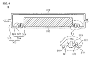
- the casing 300 includes a main body 310 having an end connected to the housing 100, and a bracket 320 provided at one side of the main body 310. Both ends of the SMPS 200 are connected to the bracket 320.
- the bracket 320 includes an extension portion 322 extending toward the inside of the casing 300 from one edge of a cut-off slot 321, which is cut off at one side of the main body 310, and a fixing portion 323 extending in parallel to one side of the casing 300 from an edge of the extension portion 322. Both ends of the SMPS 200 are connected to the fixing portion 323.
- the SMPS 200 further includes contact portions 203 connected to the fixing portions 323 at both sides thereof.
- the contact portion 203 may be disposed between the fixing portion 323, which extends from the extension portion 322, and the cut-off slot 321, and be fixed by a fastening member such as a bolt.
- FIGS. 5 to 9 can also be applied to the present invention.
- FIG 5 is a partial cut-away sectional conceptual view illustrating an overall configuration of an optical semiconductor lighting device according to another embodiment of the present invention.
- the optical semiconductor lighting device is configured such that a light emitting module 20 is arranged by a position determining unit 30 in a housing where a heat sink unit 50 is disposed.
- the housing 10 provides a space for mounting the light emitting module 20 and serves as a base of the heat sink unit 50.
- the light emitting module 20 is disposed on the bottom surface of the housing 10 and includes at least one or more semiconductor optical devices 101.
- the light emitting module 20 serves as a light source.
- the position determining unit 30 is disposed on the bottom surface of the housing 10, and corresponds to an edge of the light emitting module 20.
- the light emitting module 20 determines an accurate position, where an engine body 70 as a concept of a light engine to be described later will be mounted, and fixes the engine body 70.
- the heat sink unit 50 is disposed on the top surface of the housing 10, and is disposed at a position corresponding to the light emitting module 20, so as to discharge and cool heat generated from the light emitting module 20.
- the housing 10 provides a space for mounting and forming the light emitting module 20 and the heat sink unit 50, and further includes a main reflector 60 connected along an edge of the bottom surface of the housing 10.
- the optical semiconductor lighting device may further include an auxiliary reflector 15 having an inclined surface formed along the inside of the edge of the housing 10, that is, the edge where the main reflector 60 is mounted.
- a reflection sheet or a material for increasing reflectivity may be coated on the inclined surface of the auxiliary reflector 15.
- the outer edge of the bottom surface of the housing 10 is connected to a ring-shaped fixing frame 17, and an edge of an optical member 21 corresponding to the light emitting module 20 is fixed between the housing 10 and the fixing frame 17.
- the main reflector 60 includes a ring-shaped fixing flange 61 extending inward along the edge thereof, and the fixing flange 61 is connected to the fixing frame 17.
- optical member 21 is closely fixed by a sealing member 14 such that the edge thereof is air-tightly sealed.
- a mounting groove 13 is formed in a ring shape along the outer edge of the bottom surface of the housing 10, and a plurality of ring protrusions 135 protrude in a concentric circular shape along a direction in which the mounting groove 13 is formed.
- the sealing member 14 is connected to the mounting groove 13 from which the ring protrusions 135 protrude, and the edge of the optical member 21 is closely fixed along the inner surface of the sealing member 14.
- the sealing member 14 is finished by the fixing frame 17.
- the heat sink unit 50 discharges and cools heat generated from the light emitting module 20, and includes a plurality of heat sink fins 51 protruding from the top surface of the housing 10 in correspondence to the inner area thereof where the edge of the light emitting module 20 is formed.
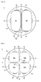
- the light emitting module 20 serves as a light source, and includes a printed circuit board on which the semiconductor optical devices 101 are arranged. As illustrated in FIGS. 6 and 7 , a plurality of mounting areas Ar1, Ar2, Ar3 and Ar4 partitioned by the position determining unit 30 are disposed on the bottom surface of the housing 10.
- the position determining unit 30 includes at least one or more first ribs 31 protruding from the bottom surface of the housing 10 in a horizontal or vertical direction, and a plurality of second ribs 32 protruding from the edge of the bottom surface of the housing 10.
- the light emitting module 20 is disposed in the plurality of mounting areas Ar1, Ar2, Ar3 and Ar4 formed between the first and second ribs 31 and 32.
- the position determining unit 30 may be configured such that the first rib 31 is arranged across the center portion of the bottom surface of the housing 10 as illustrated in FIG 6 , or may be configured such the plurality of first ribs 31 are arranged in a grid shape on a first virtual straight line l 1 disposed on the bottom surface of the housing 10 and a second virtual straight line l 2 perpendicular to the first virtual straight line l1, as illustrated in FIG 7 .
- waterproof connectors 40 are disposed at the edge of the bottom surface of the housing 10, such that the waterproof connectors 40 are connected to at least one or more external powers.
- the light emitting modules 20 may be disposed in a plurality of mounting areas Ar1 to Ar8 radially partitioned by the position determining unit 30 on the bottom surface of the housing 10, and the waterproof connectors 40 may be disposed in the center of the bottom surface of the housing 10 due to the arrangement structure.
- the position determining unit 30 includes a plurality of third ribs 33 protruding radially from the center of the bottom surface of the housing 10, and a plurality of fourth ribs 34 protruding from the edge of the bottom surface of the housing 10.
- the light emitting module 20 is disposed in a plurality of mounting areas Ar1 to Ar8 formed between the third and fourth ribs 33 and 34.
- the heat sink unit 50 may be configured to include a plurality of heat sink fins 51 formed radially from the center of the top surface of the housing 10.
- the number of the heat sink fins 51 may be approximately increased or decreased at an early stage according to the number of the semiconductor optical devices 101 and the area and output power of the light emitting module 20.
- the engine body 70 may be formed to have the top surface gradually widened from one side to the other side so as to implement an efficient arrangement structure per unit area.
- the engine body 70 refers to a structure that includes a light emitting module (not illustrated) with semiconductor optical devices, and an optical member corresponding to the light emitting module, and the engine body 70 is a structural concept extended up to a combination of a light emitting module and a power unit electrically connected thereto, which is defined in "Zhaga Consortium", the consortium for standardization of LED light engines.
- the basic technical spirit of the present invention is to provide the optical semiconductor lighting device that can significantly reduce transport costs by securing the loading space, be designed to appropriately arrange the semiconductor optical devices serving as the light source and mount the semiconductor optical devices at the accurate positions, and allow the products to be rapidly mass-produced due to the simplified manufacturing process thereof.
Abstract
Description
- The present invention relates to an optical semiconductor lighting device.
- Compared with incandescent light and fluorescent light, optical semiconductors, such as LEDs or LDs, consume low power, have a long lifespan, and have high durability and high brightness. Due to these advantages, optical semiconductors have recently attracted much attention as one of components for lighting.
- Typically, a lighting apparatus using an optical semiconductor as a light source is configured such that a power supply (hereinafter, referred to as an SMPS) is mounted on a housing in which the optical semiconductor is disposed.
- The SMPS is connected to the optical semiconductor and supplies power. Generally, a heat sink provided in the housing is interposed between the SMPS and the optical semiconductor, so that heat generated from the optical semiconductor cannot be directly transferred to the SMPS.
- However, the lighting apparatus using the optical semiconductor as the light source may be used for factory light or security light. In order to use the lighting apparatus for the above-described purpose, it is necessary to smoothly supply power, and thus, the size of the SMPS also increases.
- Therefore, the above-described SMPS protrudes from a light emitting module, which includes the optical semiconductor and is disposed in the housing, to a considerable height. Due to the protruding height of the SMPS, a space occupied by individual lighting apparatuses also increase proportionally. Hence, a large space is required for loading and transport.
- Furthermore, the lighting apparatus using the optical semiconductor is generally configured such that a plurality of optical semiconductors are disposed in a light emitting module, the light emitting module is mounted on one side of the housing, and a heat sink is disposed on the other side of the housing so as to discharge and cool heat generated from the light emitting module.
- Generally, the light emitting module may be manufactured by arranging the optical semiconductors on a printed circuit board in specific patterns. The shape of the printed circuit board may be determined according to the arranged patterns of the optical semiconductors and the shape of the housing.
- However, satisfactory research and development has not been made to check an accurate position of the housing, to which a light emitting module is to be arranged and fixed, and many related products have not been launched. Therefore, an operator has checked an appropriate position of the housing, to which the light emitting module is to be arranged and fixed, with the naked eyes. As a result, it takes a considerable time to check the position of the housing and connect the light emitting module to the housing.
- An aspect of the present invention is directed to provide an optical semiconductor lighting device that can significantly reduce transport costs by securing the loading space.
- Another aspect of the present invention is directed to provide an optical semiconductor lighting device that is designed to appropriately arrange semiconductor optical devices serving as a light source, and mount the semiconductor optical devices at accurate positions.
- Another aspect of the present invention is directed to provide an optical semiconductor lighting device that can be rapidly mass-produced due to a simplified manufacturing process thereof.
- According to an embodiment of the present invention, an optical semiconductor lighting device includes: a housing including at least one or more semiconductor optical devices; a power supply (hereinafter, SMPS) supplying power to the semiconductor optical devices; a casing accommodating the SMPS; and an adjusting unit disposed between the housing and the casing to adjust the height of the casing.
- The adjusting unit may include a rotatable assembly rotating the casing with respect to the housing.
- The adjusting unit may include: a rotatable assembly rotating the casing with respect to the housing; and a movable assembly disposed between the housing and the casing and allowing the casing to be slidable with respect to the housing.
- The rotatable assembly may include: a first portion protruding from the housing; and a second portion provided at one side of the casing and rotating around the first portion.
- The rotatable assembly may include: a latch hook formed at an end of the second portion; and a latch pin disposed at the first portion in the vicinity of a hinge pin that mutually connects the first portion and the second portion, and the latch hook may be connected to the latch pin.
- The rotatable assembly may further include a plurality of adjustment holes penetrating the first and second portions along the rotating direction of the second portion with respect to the first portion.
- The rotatable assembly may further include a fixing pin penetrating the adjustment hole of the first portion and the adjustment hole of the second portion and connecting thereto.
- The rotatable assembly may include: a third portion connected to the housing; and a second portion provided at one side of the casing and rotating around the third portion.
- The rotatable assembly may include: a latch hook formed at an end of the second portion; and a latch pin disposed at the third portion in the vicinity of a hinge pin that mutually connects the third portion and the second portion, and the latch hook may be connected to the latch pin.
- The rotatable assembly may further include a plurality of adjustment holes penetrating the second and third portions along the rotating direction of the second portion with respect to the third portion.
- The rotatable assembly may further include a fixing pin penetrating the adjustment hole of the second portion and the adjustment hole of the third portion and connecting thereto.
- The movable assembly may include: a first rail formed in the housing; and a fourth portion connected to the first rail, and the fourth portion may be connected to the rotatable assembly.
- The casing may include: a main body having an end connected to the housing; and a bracket provided at one side of the main body, and both ends of the SMPS are connected to the bracket.
- The bracket may include: a cut-off slot cut off at one side of the main body; an extension portion extending toward the inside of the casing from one edge of the cut-off slot; and a fixing portion extending from an edge of the extension portion, and both ends of the SMPS may be connected to the fixing portion.
- The SMPS may further include a contact portion connected to the fixing portion at both sides thereof.
- According to another embodiment of the present invention, an optical semiconductor lighting device includes: a housing; a light emitting module disposed on a bottom surface of the housing and including at least one or more semiconductor optical devices; a position determining unit disposed on the bottom surface of the housing and corresponding to an edge of the light emitting module; and a heat sink unit disposed on a top surface of the housing and corresponding to the light emitting module.
- The light emitting module may be disposed in a plurality of mounting areas partitioned by the position determining unit on the bottom surface of the housing.
- The optical semiconductor lighting device may further include at least one waterproof connector disposed at one side of the bottom surface of the housing.
- The light emitting module may be disposed in a plurality of mounting areas radially partitioned by the position determining unit on the bottom surface of the housing.
- The optical semiconductor lighting device may further include a waterproof connector disposed in the center of the bottom surface of the housing.
- The position determining unit may include: at least one or more first ribs protruding from the bottom surface of the housing in a horizontal or vertical direction; and a plurality of second ribs protruding from an edge of the bottom surface of the housing, wherein the light emitting module is disposed in a plurality of mounting areas between the first and second ribs.
- The first ribs of the position determining unit may be disposed across a center portion of the bottom surface of the housing.
- The first ribs of the position determining unit may be arranged on a first virtual straight line, which is disposed on the bottom surface of the housing, and a second virtual straight line, which is perpendicular to the first virtual straight line.
- The first ribs of the position determining unit may be arranged on a plurality of first virtual straight lines, which are disposed on the bottom surface of the housing, and a plurality of second virtual straight lines, which are perpendicular to the first virtual straight lines.
- The position determining unit may include: a plurality of third ribs protruding radially from the center of the bottom surface of the housing, and a plurality of fourth ribs protruding from an edge of the bottom surface of the housing, wherein the light emitting module is disposed in a plurality of mounting areas between the third and fourth ribs.
- The optical semiconductor lighting device may further include: a main reflector connected to an edge of the housing; and an auxiliary reflector having an inclined surface formed along the edge of the housing.
- The heat sink unit may include a plurality of heat sink fins protruding from the top surface of the housing in correspondence to an area where the edge of the light emitting module is formed.
- The heat sink unit may include a plurality of heat sink fins formed radially from a center of the top surface of the housing.
- According to another embodiment of the present invention, an optical semiconductor lighting device includes: a housing; at least one engine body disposed on a bottom surface of the housing and including a semiconductor optical device; a position determining unit disposed on the bottom surface of the housing and corresponding to an edge of the engine body; and a heat sink unit disposed on a top surface of the housing and corresponding to the light emitting module.
- The engine body may be formed to have a top surface gradually widened from one side to the other side.
- The term "semiconductor optical device" used in claims and the detailed description refers to light emitting diode (LED) chips or the like that includes or uses an optical semiconductor.
- The semiconductor optical devices may include package level devices with various types of optical semiconductors, including the LED chip.
- According to the present invention, the following effects can be obtained.
- The adjusting unit for adjusting the height of the casing is provided between the casing accommodating the SMPS and the housing including the semiconductor optical device. Therefore, more products can be loaded in a limited space. Furthermore, when transporting the products, logistic costs and accommodation costs can be significantly reduced.
- Due to the adjusting unit, the height of the casing can be lowered with respect to the housing, and the product can be accommodated and packaged in a box. Therefore, compared with the conventional lighting apparatus, the size of the package box can be reduced. Consequently, the amount of raw materials used can be significantly reduced, and the costs for raw materials can also be significantly reduced.
- Using the adjusting unit that can adjust the height of the casing with respect to the housing, the angle of light irradiated from the semiconductor optical device can be adjusted in an actual location where the lighting apparatus is installed, in addition to transport and loading.
- Furthermore, the position determining unit is provided on the bottom surface of the housing, such that the light emitting module or the engine body including the semiconductor optical device is appropriately arranged on the bottom surface of the housing. From this configuration, it is possible to design the appropriate arrangement structure of the semiconductor optical device serving as the light source, and it is possible to easily determine the accurate mounting position of the light emitting module or the engine body and install the light emitting module or the engine body.
- While the embodiments of the present invention have been described with reference to the specific embodiments, it will be apparent to those skilled in the art that various changes and modifications may be made without departing from the spirit and scope of the invention as defined in the following claims.
-
-
FIG 1 is a side conceptual diagram illustrating an overall configuration of an optical semiconductor lighting device according to an embodiment of the present invention. -
FIG 2 is a conceptual diagram illustrating an assembled state of an adjusting unit that is an essential part of the optical semiconductor lighting device according to the embodiment of the present invention. -
FIG 3 is a conceptual diagram illustrating an assembled state of an adjusting unit that is an essential part of an optical semiconductor lighting device according to another embodiment of the present invention. -
FIG 4 is a conceptual diagram viewed from a viewpoint B ofFIG 1 . -
FIG 5 is a partial cut-away sectional conceptual diagram illustrating an overall configuration of an optical semiconductor lighting device according to another embodiment of the present invention. -
FIGS. 6 to 8 are conceptual diagrams illustrating application examples of position determining units that are an essential part of optical semiconductor lighting devicees according to various embodiments of the present invention. -
FIG 9 is a conceptual diagram viewed from a viewpoint D ofFIG 5 . - Exemplary embodiments of the present invention will be described below in detail with reference to the accompanying drawings.
-
FIG 1 is a side conceptual diagram illustrating an overall configuration of an optical semiconductor lighting device according to an embodiment of the present invention. - As illustrated, the optical semiconductor lighting device according to the embodiment of the present invention is configured such that an adjusting
unit 500 is mounted between acasing 300 and ahousing 100. Thecasing 300 is configured to accommodate a power supply (hereinafter, referred to as an SMPS) 200. - The
housing 100 includes at least one or more semiconductoroptical devices 101, and provides a space for mounting thecasing 300 through the adjustingunit 500 which will be described later. - The
SMPS 200 supplies power to the semiconductoroptical devices 101. - The
casing 300 accommodates theSMPS 200, and is configured such that the semiconductoroptical devices 101 and theSMPS 200 are not arranged adjacent to each other through the adjustingunit 500 which will be described later. Therefore, thecasing 300 prevents heat generated from the semiconductoroptical devices 101 from being directly transferred to theSMPS 200. - The adjusting
unit 500 is arranged between thehousing 100 and thecasing 300, and serves to change the height of thecasing 300 protruding from thehousing 100. - Therefore, when installed and used in the actual fields, the adjusting
unit 500 may be arranged vertically to the top surface of thehousing 100, like the position of thecasing 300 indicated by dotted lines inFIG 1 . - Also, when it is necessary to reduce a total volume upon loading and transport, the adjusting
unit 500 may be arranged in parallel to the top surface of thehousing 100, like the position of thecasing 300 indicated by solid lines. - It is apparent that the following various embodiments as well as the above-described embodiment can also be applied to the present invention.
- As described above, the
housing 100 includes semiconductoroptical devices 101, a heat sink 110 disposed in the vicinity of the semiconductoroptical devices 101 so as to discharge heat generated from the semiconductoroptical devices 101, and a reflector 120 extending along an edge of an area where the semiconductoroptical devices 101 are disposed. - Meanwhile, as described above, the adjusting
unit 500 changes the height of thecasing 300 with respect to thehousing 100, and may include arotatable assembly 510 for rotating thecasing 300 with respect to thehousing 100. - That is, the
rotatable assembly 510 includes afirst portion 511 protruding from thehousing 100, and asecond portion 512 provided at one side of thecasing 300 and rotating around thefirst portion 511. - The
rotatable assembly 510 includes alatch hook 514 at an end of thesecond portion 512. Alatch pin 515 is disposed at thefirst portion 511 in the vicinity of ahinge pin 519 that mutually connects thefirst portion 511 and thesecond portion 512. Thelatch hook 514 is connected to thelatch pin 515. - In addition, as illustrated in
FIG 2 , therotatable assembly 510 may further include a plurality of adjustment holes 516 penetrating the first andsecond portions second portion 512 with respect to thefirst portion 511, so as to adjust a tilt angle of thehousing 100 with respect to thecasing 300. - The
rotatable assembly 510 may include a fixing pin 517 (see an assembled state ofFIG 3 ) penetrating theadjustment hole 516 of thefirst portion 511 and theadjustment hole 516 of thesecond portion 512 and connecting thereto, so as to maintain a state in which the tilt angle of thehousing 100 is adjusted with respect to thecasing 300. - In this case, as illustrated in
FIG 3 , therotatable assembly 510 may further include a third portion 513 detachably connected to thehousing 100, instead of thefirst portion 511 integrally formed in thehousing 100 as illustrated inFIGS. 1 and 2 , and asecond portion 512 provided at one side of thecasing 300 and rotating around the third portion 513. - In the embodiment of
FIG 3 , applications and design modification can also be made such that therotatable assembly 510 includes thelatch hook 514 and thelatch pin 515 as illustrated inFIGS. 1 and 2 , and the plurality of adjustment holes 516 are formed so that thelatch hook 514 and thelatch pin 515 are fixed together by the fixingpin 517. - Meanwhile, the
adjustment unit 500 may include amovable assembly 520 that is disposed between thehousing 100 and thecasing 300 together with therotatable assembly 510 and allows thecasing 300 to be slidable with respect to thehousing 100. - In this case, as illustrated in
FIG 3 , themovable assembly 520 includes afirst rail 521 formed in thehousing 100, and afourth portion 524 connected to thefirst rail 521, and thefourth portion 524 is connected to therotatable assembly 510, that is, the third portion 513. - Meanwhile, as described above, the
casing 300 provides the space for accommodating theSMPS 200, and may be made of aluminum or an aluminum alloy having superior heat dissipation performance. As illustrated inFIG 4 , thecasing 300 includes amain body 310 having an end connected to thehousing 100, and abracket 320 provided at one side of themain body 310. Both ends of theSMPS 200 are connected to thebracket 320. - The
bracket 320 includes anextension portion 322 extending toward the inside of thecasing 300 from one edge of a cut-off slot 321, which is cut off at one side of themain body 310, and a fixingportion 323 extending in parallel to one side of thecasing 300 from an edge of theextension portion 322. Both ends of theSMPS 200 are connected to the fixingportion 323. - In this case, the
SMPS 200 further includescontact portions 203 connected to the fixingportions 323 at both sides thereof. As illustrated, thecontact portion 203 may be disposed between the fixingportion 323, which extends from theextension portion 322, and the cut-off slot 321, and be fixed by a fastening member such as a bolt. - Meanwhile, embodiments of
FIGS. 5 to 9 can also be applied to the present invention. -
FIG 5 is a partial cut-away sectional conceptual view illustrating an overall configuration of an optical semiconductor lighting device according to another embodiment of the present invention. - As illustrated, the optical semiconductor lighting device according to the embodiment of the present invention is configured such that a
light emitting module 20 is arranged by aposition determining unit 30 in a housing where aheat sink unit 50 is disposed. - First, the
housing 10 provides a space for mounting thelight emitting module 20 and serves as a base of theheat sink unit 50. - The
light emitting module 20 is disposed on the bottom surface of thehousing 10 and includes at least one or more semiconductoroptical devices 101. Thelight emitting module 20 serves as a light source. - The
position determining unit 30 is disposed on the bottom surface of thehousing 10, and corresponds to an edge of thelight emitting module 20. Thelight emitting module 20 determines an accurate position, where an engine body 70 as a concept of a light engine to be described later will be mounted, and fixes the engine body 70. - In addition, the
heat sink unit 50 is disposed on the top surface of thehousing 10, and is disposed at a position corresponding to thelight emitting module 20, so as to discharge and cool heat generated from thelight emitting module 20. - It is apparent that the following various embodiments as well as the above-described embodiment can also be applied to the present invention.
- As described above, the
housing 10 provides a space for mounting and forming thelight emitting module 20 and theheat sink unit 50, and further includes amain reflector 60 connected along an edge of the bottom surface of thehousing 10. - In this case, the optical semiconductor lighting device may further include an
auxiliary reflector 15 having an inclined surface formed along the inside of the edge of thehousing 10, that is, the edge where themain reflector 60 is mounted. - Although not specifically illustrated, a reflection sheet or a material for increasing reflectivity may be coated on the inclined surface of the
auxiliary reflector 15. - To be specific, the outer edge of the bottom surface of the
housing 10 is connected to a ring-shapedfixing frame 17, and an edge of anoptical member 21 corresponding to thelight emitting module 20 is fixed between thehousing 10 and the fixingframe 17. - The
main reflector 60 includes a ring-shaped fixingflange 61 extending inward along the edge thereof, and the fixingflange 61 is connected to the fixingframe 17. - In addition, the
optical member 21 is closely fixed by a sealingmember 14 such that the edge thereof is air-tightly sealed. - To be specific, a mounting
groove 13 is formed in a ring shape along the outer edge of the bottom surface of thehousing 10, and a plurality ofring protrusions 135 protrude in a concentric circular shape along a direction in which the mountinggroove 13 is formed. - The sealing
member 14 is connected to the mountinggroove 13 from which thering protrusions 135 protrude, and the edge of theoptical member 21 is closely fixed along the inner surface of the sealingmember 14. The sealingmember 14 is finished by the fixingframe 17. - Furthermore, as described above, the
heat sink unit 50 discharges and cools heat generated from thelight emitting module 20, and includes a plurality ofheat sink fins 51 protruding from the top surface of thehousing 10 in correspondence to the inner area thereof where the edge of thelight emitting module 20 is formed. - Meanwhile, as described above, the
light emitting module 20 serves as a light source, and includes a printed circuit board on which the semiconductoroptical devices 101 are arranged. As illustrated inFIGS. 6 and 7 , a plurality of mounting areas Ar1, Ar2, Ar3 and Ar4 partitioned by theposition determining unit 30 are disposed on the bottom surface of thehousing 10. - The
position determining unit 30 includes at least one or morefirst ribs 31 protruding from the bottom surface of thehousing 10 in a horizontal or vertical direction, and a plurality ofsecond ribs 32 protruding from the edge of the bottom surface of thehousing 10. - Therefore, the
light emitting module 20 is disposed in the plurality of mounting areas Ar1, Ar2, Ar3 and Ar4 formed between the first andsecond ribs - That is, the
position determining unit 30 may be configured such that thefirst rib 31 is arranged across the center portion of the bottom surface of thehousing 10 as illustrated inFIG 6 , or may be configured such the plurality offirst ribs 31 are arranged in a grid shape on a first virtual straight line ℓ 1 disposed on the bottom surface of thehousing 10 and a second virtualstraight line ℓ 2 perpendicular to the first virtual straight line ℓ1, as illustrated inFIG 7 . - In this case,
waterproof connectors 40 are disposed at the edge of the bottom surface of thehousing 10, such that thewaterproof connectors 40 are connected to at least one or more external powers. - Meanwhile, as illustrated in
FIG 8 , thelight emitting modules 20 may be disposed in a plurality of mounting areas Ar1 to Ar8 radially partitioned by theposition determining unit 30 on the bottom surface of thehousing 10, and thewaterproof connectors 40 may be disposed in the center of the bottom surface of thehousing 10 due to the arrangement structure. - To be specific, the
position determining unit 30 includes a plurality ofthird ribs 33 protruding radially from the center of the bottom surface of thehousing 10, and a plurality offourth ribs 34 protruding from the edge of the bottom surface of thehousing 10. - In this case, the
light emitting module 20 is disposed in a plurality of mounting areas Ar1 to Ar8 formed between the third andfourth ribs - Therefore, as illustrated in
FIG 9 , theheat sink unit 50 may be configured to include a plurality ofheat sink fins 51 formed radially from the center of the top surface of thehousing 10. - In designing the
heat sink fins 51, the number of theheat sink fins 51 may be approximately increased or decreased at an early stage according to the number of the semiconductoroptical devices 101 and the area and output power of thelight emitting module 20. - Furthermore, applications and design modifications can also be made such that the structure of the engine body 70 including semiconductor optical devices (not illustrated) instead of the
light emitting module 20, , that is, the concept of the light engine, is disposed in the plurality of mounting areas Ar1 to Ar8 partitioned by theposition determining unit 30. - In this case, the engine body 70 may be formed to have the top surface gradually widened from one side to the other side so as to implement an efficient arrangement structure per unit area.
- Although not specifically illustrated, it should be understood that the engine body 70 refers to a structure that includes a light emitting module (not illustrated) with semiconductor optical devices, and an optical member corresponding to the light emitting module, and the engine body 70 is a structural concept extended up to a combination of a light emitting module and a power unit electrically connected thereto, which is defined in "Zhaga Consortium", the consortium for standardization of LED light engines.
- As described above, the basic technical spirit of the present invention is to provide the optical semiconductor lighting device that can significantly reduce transport costs by securing the loading space, be designed to appropriately arrange the semiconductor optical devices serving as the light source and mount the semiconductor optical devices at the accurate positions, and allow the products to be rapidly mass-produced due to the simplified manufacturing process thereof.
Claims (30)
- An optical semiconductor lighting device, comprising:a housing including at least one or more semiconductor optical devices;a power supply (hereinafter, SMPS) supplying power to the semiconductor optical devices;a casing accommodating the SMPS; andan adjusting unit disposed between the housing and the casing to adjust the height of the casing.
- The optical semiconductor lighting device of claim 1, wherein the adjusting unit comprises a rotatable assembly rotating the casing with respect to the housing.
- The optical semiconductor lighting device of claim 1, wherein the adjusting unit comprises:a rotatable assembly rotating the casing with respect to the housing; anda movable assembly disposed between the housing and the casing and allowing the casing to be slidable with respect to the housing.
- The optical semiconductor lighting device of claim 2 or 3, wherein the rotatable assembly comprises:a first portion protruding from the housing; anda second portion provided at one side of the casing and rotating around the first portion.
- The optical semiconductor lighting device of claim 2 or 3, wherein the rotatable assembly comprises:a third portion connected to the housing; anda second portion provided at one side of the casing and rotating around the third portion.
- The optical semiconductor lighting device of claim 3, wherein
the movable assembly comprises:a first rail formed in the housing; anda fourth portion connected to the first rail, andthe fourth portion is connected to the rotatable assembly. - The optical semiconductor lighting device of claim 1, wherein
the casing comprises:a main body having an end connected to the housing; anda bracket provided at one side of the main body, andboth ends of the SMPS are connected to the bracket. - The optical semiconductor lighting device of claim 7, wherein
the bracket comprises:a cut-off slot cut off at one side of the main body;an extension portion extending toward the inside of the casing from one edge of the cut-off slot; anda fixing portion extending from an edge of the extension portion, andboth ends of the SMPS are connected to the fixing portion. - The optical semiconductor lighting device of claim 8, wherein the SMPS further comprises a contact portion connected to the fixing portion at both sides thereof.
- The optical semiconductor lighting device of claim 4, wherein
the rotatable assembly comprises:a latch hook formed at an end of the second portion; anda latch pin disposed at the first portion in the vicinity of a hinge pin that mutually connects the first portion and the second portion, andthe latch hook is connected to the latch pin. - The optical semiconductor lighting device of claim 4, wherein the rotatable assembly further comprises a plurality of adjustment holes penetrating the first and second portions along the rotating direction of the second portion with respect to the first portion.
- The optical semiconductor lighting device of claim 11, wherein the rotatable assembly further comprises a fixing pin penetrating the adjustment hole of the first portion and the adjustment hole of the second portion and connecting thereto.
- The optical semiconductor lighting device of claim 5, wherein
the rotatable assembly comprises:a latch hook formed at an end of the second portion; anda latch pin disposed at the third portion in the vicinity of a hinge pin that mutually connects the third portion and the second portion, andthe latch hook is connected to the latch pin. - The optical semiconductor lighting device of claim 5, wherein the rotatable assembly further comprises a plurality of adjustment holes penetrating the second and third portions along the rotating direction of the second portion with respect to the third portion.
- The optical semiconductor lighting device of claim 14, wherein the rotatable assembly further comprises a fixing pin penetrating the adjustment hole of the second portion and the adjustment hole of the third portion and connecting thereto.
- An optical semiconductor lighting device, comprising:a housing;a light emitting module disposed on a bottom surface of the housing and including at least one or more semiconductor optical devices;a position determining unit disposed on the bottom surface of the housing and corresponding to an edge of the light emitting module; anda heat sink unit disposed on a top surface of the housing and corresponding to the light emitting module.
- The optical semiconductor lighting device of claim 16, wherein the light emitting module is disposed in a plurality of mounting areas partitioned by the position determining unit on the bottom surface of the housing.
- The optical semiconductor lighting device of claim 17, further comprising at least one waterproof connector disposed at one side of the bottom surface of the housing.
- The optical semiconductor lighting device of claim 16, wherein the light emitting module is disposed in a plurality of mounting areas radially partitioned by the position determining unit on the bottom surface of the housing.
- The optical semiconductor lighting device of claim 19, further comprising a waterproof connector disposed in the center of the bottom surface of the housing.
- The optical semiconductor lighting device of claim 16, wherein the position determining unit comprises:at least one or more first ribs protruding from the bottom surface of the housing in a horizontal or vertical direction; anda plurality of second ribs protruding from an edge of the bottom surface of the housing,wherein the light emitting module is disposed in a plurality of mounting areas between the first and second ribs.
- The optical semiconductor lighting device of claim 21, wherein the first ribs of the position determining unit are disposed across a center portion of the bottom surface of the housing.
- The optical semiconductor lighting device of claim 21, wherein the first ribs of the position determining unit are arranged on a first virtual straight line, which is disposed on the bottom surface of the housing, and a second virtual straight line, which is perpendicular to the first virtual straight line.
- The optical semiconductor lighting device of claim 16, wherein the first ribs of the position determining unit are arranged on a plurality of first virtual straight lines, which are disposed on the bottom surface of the housing, and a plurality of second virtual straight lines, which are perpendicular to the first virtual straight lines.
- The optical semiconductor lighting device of claim 16, wherein the position determining unit comprises:a plurality of third ribs protruding radially from the center of the bottom surface of the housing, anda plurality of fourth ribs protruding from an edge of the bottom surface of the housing,wherein the light emitting module is disposed in a plurality of mounting areas between the third and fourth ribs.
- The optical semiconductor lighting device of claim 16, further comprising:a main reflector connected to an edge of the housing; andan auxiliary reflector having an inclined surface formed along the edge of the housing.
- The optical semiconductor lighting device of claim 16, wherein the heat sink unit comprises a plurality of heat sink fins protruding from the top surface of the housing in correspondence to an area where the edge of the light emitting module is formed.
- The optical semiconductor lighting device of claim 16, wherein the heat sink unit comprises a plurality of heat sink fins formed radially from a center of the top surface of the housing.
- An optical semiconductor lighting device, comprising:a housing;at least one engine body disposed on a bottom surface of the housing and including a semiconductor optical device;a position determining unit disposed on the bottom surface of the housing and corresponding to an edge of the engine body; anda heat sink unit disposed on a top surface of the housing and corresponding to the light emitting module.
- The optical semiconductor lighting device of claim 29, wherein the engine body is formed to have a top surface gradually widened from one side to the other side.
Applications Claiming Priority (3)
| Application Number | Priority Date | Filing Date | Title |
|---|---|---|---|
| KR1020120072919A KR101347386B1 (en) | 2012-07-04 | 2012-07-04 | Optical semiconductor illuminating apparatus |
| KR1020120077197A KR101347387B1 (en) | 2012-07-16 | 2012-07-16 | Optical semiconductor illuminating apparatus |
| PCT/KR2012/006768 WO2014007426A1 (en) | 2012-07-04 | 2012-08-24 | Optical semiconductor lighting device |
Publications (2)
| Publication Number | Publication Date |
|---|---|
| EP2871410A1 true EP2871410A1 (en) | 2015-05-13 |
| EP2871410A4 EP2871410A4 (en) | 2016-01-20 |
Family
ID=49396779
Family Applications (1)
| Application Number | Title | Priority Date | Filing Date |
|---|---|---|---|
| EP12880686.6A Withdrawn EP2871410A4 (en) | 2012-07-04 | 2012-08-24 | Optical semiconductor lighting device |
Country Status (6)
| Country | Link |
|---|---|
| US (2) | US9010962B2 (en) |
| EP (1) | EP2871410A4 (en) |
| JP (3) | JP5296251B1 (en) |
| CN (1) | CN104272019A (en) |
| AU (1) | AU2012384645B2 (en) |
| WO (1) | WO2014007426A1 (en) |
Families Citing this family (5)
| Publication number | Priority date | Publication date | Assignee | Title |
|---|---|---|---|---|
| ES1093730Y (en) * | 2013-10-24 | 2014-02-13 | Simon S A U | LUMINARY |
| US10429055B2 (en) * | 2014-04-04 | 2019-10-01 | Lg Innotek Co., Ltd. | Lighting module and lighting apparatus including same |
| KR101722682B1 (en) * | 2015-01-02 | 2017-04-04 | 주식회사 케이엠더블유 | LED lighting device that directly connected to the power supply |
| JP2016181436A (en) * | 2015-03-24 | 2016-10-13 | 東芝ライテック株式会社 | Lighting device |
| IT201800003668A1 (en) * | 2018-03-16 | 2019-09-16 | Fael Spa | Molding process for obtaining a symmetrical or asymmetrical projector |
Family Cites Families (26)
| Publication number | Priority date | Publication date | Assignee | Title |
|---|---|---|---|---|
| US2123695A (en) * | 1937-10-08 | 1938-07-12 | L A Darling Company | Article display fixture |
| US4378584A (en) * | 1981-05-04 | 1983-03-29 | Keene Corporation | Hanging light fixture mounting arrangement |
| US4489910A (en) * | 1982-05-24 | 1984-12-25 | Ferguson Joseph D | Mounting bracket for traffic signal installation |
| US4661892A (en) * | 1985-07-01 | 1987-04-28 | Emerson Electric Co. | Electrical plug and receptacle for lighting fixture power hook |
| KR20070001445A (en) * | 2005-06-29 | 2007-01-04 | 김진구 | Lighting apparatus for the working of dent removal of cars |
| DE102007050893B4 (en) * | 2007-10-24 | 2011-06-01 | Continental Automotive Gmbh | Method for positioning and mounting a LED assembly and positioning body therefor |
| JP2009129809A (en) | 2007-11-27 | 2009-06-11 | Toshiba Lighting & Technology Corp | Lighting system |
| KR100999162B1 (en) | 2008-03-24 | 2010-12-07 | 주식회사 아모럭스 | Lighting apparatus using light emitting diode |
| JP2010010124A (en) * | 2008-05-28 | 2010-01-14 | Toshiba Lighting & Technology Corp | Lighting system |
| JP5391767B2 (en) * | 2008-05-30 | 2014-01-15 | 東芝ライテック株式会社 | Light emitting device and lighting apparatus |
| US8602601B2 (en) * | 2009-02-11 | 2013-12-10 | Koninklijke Philips N.V. | LED downlight retaining ring |
| US20120086885A1 (en) | 2009-06-15 | 2012-04-12 | Sharp Kabushiki Kaisha | Lighting device, display device and television receiver |
| US20110002124A1 (en) * | 2009-07-06 | 2011-01-06 | Kun-Jung Chang | Wide angle led lamp structure |
| KR100949452B1 (en) * | 2009-08-19 | 2010-03-29 | 주식회사 누리플랜 | Led lighting device |
| KR20120081019A (en) | 2009-09-30 | 2012-07-18 | 파나소닉 주식회사 | Illumination device |
| JP4423574B2 (en) | 2009-10-20 | 2010-03-03 | 東芝ライテック株式会社 | Lighting device |
| KR101077476B1 (en) * | 2009-11-03 | 2011-10-28 | 주식회사 삼진엘앤디 | Variable-length LED lamp |
| US8727564B2 (en) * | 2010-01-26 | 2014-05-20 | Toshiba Lighting & Technology Corporation | Illumination apparatus |
| JP2011159447A (en) * | 2010-01-29 | 2011-08-18 | Toshiba Lighting & Technology Corp | Lighting system |
| JP2011204655A (en) * | 2010-03-26 | 2011-10-13 | Toshiba Lighting & Technology Corp | Lighting fixture |
| CN201696993U (en) * | 2010-06-08 | 2011-01-05 | 东莞勤上光电股份有限公司 | LED road lamp, and power supply component and light source component thereof |
| CN101943339B (en) * | 2010-08-04 | 2011-11-16 | 东莞市光烨节能科技有限公司 | Led illuminating lamp |
| US8480268B2 (en) * | 2010-08-18 | 2013-07-09 | Hubbell Incorporated | Electrical box and ballast mounting assembly for retrofitting recessed lighting fixtures |
| FI20106200A (en) * | 2010-11-15 | 2012-05-16 | Ensto Finland Oy | Lamp |
| JP3168300U (en) * | 2011-01-26 | 2011-06-09 | 日本発條株式会社 | Floodlight waterproof structure |
| WO2012164506A1 (en) * | 2011-05-31 | 2012-12-06 | Sabic Innovative Plastics Ip B.V. | Led plastic heat sink and method for making and using the same |
-
2012
- 2012-08-24 WO PCT/KR2012/006768 patent/WO2014007426A1/en active Application Filing
- 2012-08-24 EP EP12880686.6A patent/EP2871410A4/en not_active Withdrawn
- 2012-08-24 AU AU2012384645A patent/AU2012384645B2/en not_active Ceased
- 2012-08-24 CN CN201280073025.3A patent/CN104272019A/en active Pending
- 2012-08-28 US US13/596,580 patent/US9010962B2/en not_active Expired - Fee Related
- 2012-08-31 JP JP2012191845A patent/JP5296251B1/en not_active Expired - Fee Related
-
2013
- 2013-06-11 JP JP2013122457A patent/JP5685289B2/en not_active Expired - Fee Related
-
2015
- 2015-01-15 JP JP2015005604A patent/JP2015079770A/en active Pending
- 2015-03-12 US US14/656,313 patent/US20150184836A1/en not_active Abandoned
Also Published As
| Publication number | Publication date |
|---|---|
| WO2014007426A1 (en) | 2014-01-09 |
| AU2012384645A1 (en) | 2014-09-11 |
| CN104272019A (en) | 2015-01-07 |
| JP5296251B1 (en) | 2013-09-25 |
| JP2014013755A (en) | 2014-01-23 |
| EP2871410A4 (en) | 2016-01-20 |
| US20140009933A1 (en) | 2014-01-09 |
| AU2012384645B2 (en) | 2015-07-09 |
| JP2014013743A (en) | 2014-01-23 |
| US9010962B2 (en) | 2015-04-21 |
| US20150184836A1 (en) | 2015-07-02 |
| JP2015079770A (en) | 2015-04-23 |
| JP5685289B2 (en) | 2015-03-18 |
Similar Documents
| Publication | Publication Date | Title |
|---|---|---|
| EP1914470B1 (en) | Semiconductor lamp | |
| US8915618B2 (en) | Optical semiconductor lighting apparatus | |
| US20150184836A1 (en) | Optical semiconductor lighting apparatus | |
| US20090323342A1 (en) | Led illumination device | |
| WO2011052639A1 (en) | Led lighting device | |
| US9076952B2 (en) | Semiconductor light-emitting device | |
| KR20150042567A (en) | Light source module and method of manufacturing the same | |
| US20120327638A1 (en) | Illumination appliance | |
| EP2775195B1 (en) | Led tri-proof lamp | |
| CN104246353A (en) | Lamp and lighting apparatus | |
| EP3234460B1 (en) | Illumination device | |
| KR101722682B1 (en) | LED lighting device that directly connected to the power supply | |
| KR20120088688A (en) | Led lamps with packaging as a kit | |
| US10288274B2 (en) | LED lighting apparatus having flame barriers | |
| CN104048197A (en) | Illumination light source and lighting apparatus | |
| US20150070911A1 (en) | Optical semiconductor lighting apparatus | |
| KR20130090264A (en) | Illuminating device | |
| AU2015201092A1 (en) | Optical semiconductor lighting device | |
| EP3800396B1 (en) | Vehicle light fixture | |
| US10125966B2 (en) | Light emitting diode lamps with heat-dispersing construction and mechanism | |
| US20150192287A1 (en) | Lighting device comprising a heat sink structure | |
| KR101347387B1 (en) | Optical semiconductor illuminating apparatus | |
| JP6442871B2 (en) | Vehicle lighting | |
| KR101196645B1 (en) | Led heat sink apparatus | |
| US20230250939A1 (en) | Explosion-Proof Luminaire |
Legal Events
| Date | Code | Title | Description |
|---|---|---|---|
| PUAI | Public reference made under article 153(3) epc to a published international application that has entered the european phase |
Free format text: ORIGINAL CODE: 0009012 |
|
| 17P | Request for examination filed |
Effective date: 20141007 |
|
| AK | Designated contracting states |
Kind code of ref document: A1 Designated state(s): AL AT BE BG CH CY CZ DE DK EE ES FI FR GB GR HR HU IE IS IT LI LT LU LV MC MK MT NL NO PL PT RO RS SE SI SK SM TR |
|
| AX | Request for extension of the european patent |
Extension state: BA ME |
|
| RIN1 | Information on inventor provided before grant (corrected) |
Inventor name: YOO, MIN UK Inventor name: KIM, MIN SU Inventor name: KIM, JUNG HWA Inventor name: KIM, JI WAN |
|
| DAX | Request for extension of the european patent (deleted) | ||
| RA4 | Supplementary search report drawn up and despatched (corrected) |
Effective date: 20151223 |
|
| RIC1 | Information provided on ipc code assigned before grant |
Ipc: F21V 21/14 20060101ALI20151217BHEP Ipc: F21V 23/00 20150101ALI20151217BHEP Ipc: F21V 17/02 20060101AFI20151217BHEP |
|
| STAA | Information on the status of an ep patent application or granted ep patent |
Free format text: STATUS: THE APPLICATION IS DEEMED TO BE WITHDRAWN |
|
| 18D | Application deemed to be withdrawn |
Effective date: 20160722 |