EP2870538B1 - Synchronisation einer dispergierten raid-gruppe - Google Patents
Synchronisation einer dispergierten raid-gruppe Download PDFInfo
- Publication number
- EP2870538B1 EP2870538B1 EP13813635.3A EP13813635A EP2870538B1 EP 2870538 B1 EP2870538 B1 EP 2870538B1 EP 13813635 A EP13813635 A EP 13813635A EP 2870538 B1 EP2870538 B1 EP 2870538B1
- Authority
- EP
- European Patent Office
- Prior art keywords
- memory
- time
- data
- modules
- epoch
- Prior art date
- Legal status (The legal status is an assumption and is not a legal conclusion. Google has not performed a legal analysis and makes no representation as to the accuracy of the status listed.)
- Active
Links
Images


Classifications
-
- G—PHYSICS
- G06—COMPUTING OR CALCULATING; COUNTING
- G06F—ELECTRIC DIGITAL DATA PROCESSING
- G06F3/00—Input arrangements for transferring data to be processed into a form capable of being handled by the computer; Output arrangements for transferring data from processing unit to output unit, e.g. interface arrangements
- G06F3/06—Digital input from, or digital output to, record carriers, e.g. RAID, emulated record carriers or networked record carriers
- G06F3/0601—Interfaces specially adapted for storage systems
- G06F3/0668—Interfaces specially adapted for storage systems adopting a particular infrastructure
- G06F3/0671—In-line storage system
- G06F3/0683—Plurality of storage devices
- G06F3/0689—Disk arrays, e.g. RAID, JBOD
-
- G—PHYSICS
- G06—COMPUTING OR CALCULATING; COUNTING
- G06F—ELECTRIC DIGITAL DATA PROCESSING
- G06F11/00—Error detection; Error correction; Monitoring
- G06F11/07—Responding to the occurrence of a fault, e.g. fault tolerance
- G06F11/08—Error detection or correction by redundancy in data representation, e.g. by using checking codes
- G06F11/10—Adding special bits or symbols to the coded information, e.g. parity check, casting out 9's or 11's
- G06F11/1076—Parity data used in redundant arrays of independent storages, e.g. in RAID systems
- G06F11/108—Parity data distribution in semiconductor storages, e.g. in SSD
-
- G—PHYSICS
- G06—COMPUTING OR CALCULATING; COUNTING
- G06F—ELECTRIC DIGITAL DATA PROCESSING
- G06F13/00—Interconnection of, or transfer of information or other signals between, memories, input/output devices or central processing units
- G06F13/14—Handling requests for interconnection or transfer
Definitions
- the present application may relate to the storage of digital data in a plurality of storage devices.
- Reliable storage of digital data in a memory system is effected by using error correcting codes, erasure codes, redundant data storage, or the like.
- One method of storing data in a reliable way is to use a RAID (Reliable Array of Inexpensive Disks) architecture. Except for RAID 0 (which does not provide redundancy), the various RAID types (e.g. 1, 3, 4, 5, 6, etc.) store an extent of data by writing chunks of the data to several independent memories and redundancy data to other independent memories, with the objective that, should one or more of the memories encounter a failure, the data can be recovered from the remaining stored data.
- RAID Reliable Array of Inexpensive Disks
- a stripe of data comprising a plurality of strips of data may be written, the strips being chunks of data of the extent of data, such that each of the strips of the stripe is written to a separate disk, and a parity strip is computed over the chunks of data and stored to another disk.
- the loss of a disk storing a chunk of the extent may be overcome by computing the exclusive-OR of the remaining chunks and the parity data to produce the lost data.
- This is a simple example of single-parity RAID, but a person of skill in the art would understand the extension to multiple parity, distributed parity, and other similar techniques which may provide protection against the loss of multiple disks.
- non-volatile solid state memory has been reduced, primarily due to the increase production of NAND flash devices for use in consumer electronics such as cell phones, tablets, audio players and the like.
- Memory systems using NAND flash have been produced that emulate the protocols of rotating disks, and such SCSI-compatible devices, for example, are now found in laptops and have been used in arrays to replace mechanical disks in larger storage systems.
- Flash memory has its own limitations, which may be characterized as being related to timing and wear out.
- Data is stored in a flash memory circuit in pages, with a plurality of pages forming a block, and a plurality of blocks being found in a memory circuit ("a chip').
- a characteristic of NAND flash memory is that while data may be written in pages in sequential order, the memory cannot be overwritten without being first erased, and the erase operation must be performed on integral blocks.
- the page read time, page write time and block erase time are not the same time duration, with the write time typically being a multiple of the read time and the block erase time typically being a multiple of the write time. Although these times vary with the specific NAND flash type and manufacturer, an example would be read time (100us), write time (500us) and block erase time (5ms).
- RAID may be used in a flash memory system.
- each chip may be in a different state when a request for data from a RAID stripe is received. That is, the chip may be performing, for example, a write or an erase operation and not be available to read data until the write or erase operation has completed.
- the technique is termed "erase hiding.” This is not intended to exclude an aspect of the technique that may be called “write hiding”. As will be seen, the erase hiding and write hiding are both performed in a similar manner, and may often be combined, where the choice of performing a write operation or an erase operation may depend on the nature of the pending operations for any memory chip.
- the term "erase hiding” is understood to mean that the operations of the memory system are scheduled or controlled such that there are periods of time where operations that could interfere with low-latency reading of data from the memory system are either inhibited or permitted so as to permit low-latency read operations to be routinely performed. Where such operations are not pending, the particular memory module may also perform read or write operations, some of which may be background operations.
- chip is used to signify a memory circuit having a plurality of blocks of storage locations, or pages, and may include a plurality of memory circuits in a memory package, a plurality of memory packages, and even larger scale assemblies that are operated in a coordinated and consistent manner.
- WO 2008/121306 describes a memory system and method of operating the memory system as a RAID array.
- the writing of data, for low-write data loads, is managed such that only one of the memory modules of a RAID stripe is being written to, or erased, during a time interval.
- WO 2011/044515 describes data stored using a RAID data storage array with the reading, writing and erasing operations arranged such that the erasing and writing operations may be performed without significant latency for performing a read operation.
- a memory storage system having a plurality of memory units, each unit further comprising a plurality of memory modules.
- a group of memory modules selected from two or more memory units are configured to perform coordinated operations.
- the memory modules are synchronised using a communications path for transmitting a synchronisation signal produced by a synchronisation signal generator, and the synchronisation signal is distributed to the groups of memory.
- a memory unit has a memory module clock to generate a local synchronisation signal based upon the synchronisation signal received over the communications path and transmit the local synchronisation signal to a group memory modules of the memory unit.
- the memory unit may have an electronic circuit operable to count the cycles of a memory unit clock oscillator and to determine and maintain a duration value of an epoch of time for the unit and an epoch start time for the unit. These maintained quantities may be compared with the received synchronization signal, and the maintained quantities may be adjusted to reduce the difference between the received synchronization signal and the maintained epoch time or the maintained epoch start time.
- the local synchronization signal may be distributed to the memory modules.
- a memory module of the plurality of memory module may have an electronic circuit configured to count the cycles of the memory module clock oscillator and determine and maintain a duration value of an epoch of time and maintain an epoch start time. These maintained values may be compared with the duration of the epoch time and the epoch time derived from the synchronization generator signal received over the communication path or from a local synchronization signal and used to adjust one of a frequency of oscillation of the clock oscillator in the memory module or the number of counts of the memory module clock for an epoch of time so as to reduce the difference in time between the received synchronization generator signal and the computed epoch time.
- the synchronization signal generator may be a disciplined oscillator, and the controlling input may be from a global navigation system such as the Global Positioning System (GPS)
- GPS Global Positioning System
- the groups of memory modules may be selected so as to form RAID groups, where a group of memory modules is selected from two or more memory units so as to form a RAID group and the epochs of the RAID group are synchronized such that the RAID group exhibits erase hiding performance.
- a memory storage system may have a plurality of memory units, each unit further comprising a plurality of memory modules where a group of memory modules is selected from two or more memory units so as to form a RAID group.
- the memory system is operable such that the epochs of the RAID group may be synchronized such that the RAID group exhibits erase hiding performance.
- a synchronization signal from a synchronization signal circuit is distributed to the plurality of memory unit, and a local synchronization signal is distributed to the memory modules.
- each memory module of the group of memory modules may have a clock and an electronic circuit configured to count the cycles of a clock oscillator and determine and maintain a duration value of an epoch of time, and a start time for an epoch at the memory module.
- the memory system is further operable to compare the duration value of the maintained epoch time, and an alignment of the maintained start time of the epoch, determined from a synchronization signal; and, align a start time of an epoch with the synchronization signal.
- the memory system may correct one of a frequency of oscillation of the clock oscillator in the memory module or the number of counts of the memory module clock for an epoch of time so as to reduce the difference in time between the received synchronization signal and the maintained epoch time or the difference between the maintained start time of an epoch and the received synchronization signal.
- the synchronization signal may be the IEEE 1588 protocol.
- the synchronization signal may be one of a GPS received 1 pps (pulse per second) output, or a synchronization signal derived therefrom.
- a memory system may include a plurality of memory units, each memory unit comprising a plurality of memory modules, where a group of the plurality of memory modules of at least two memory units are configured to perform a related storage operation.
- the system includes a means for coordinating the performance of the related storage operation based on a time synchronization of the groups of memory modules of the at least two memory units.
- the related storage operation may be the reading of data stored in the groups of memory modules and the groups of memory modules are configured as a RAID group, and the result of coordination of the performance of the related storage operation is erase hiding.
- the memory modules may comprise NAND flash memory.
- a method of operating a data storage system is described where the data storage system comprises at least two memory units, each memory unit comprising a plurality of memory modules, and the method may include the steps of: selecting a group of memory modules of a first memory unit and a group of memory modules of a second group of memory modules; synchronizing the performance of a storage operation resulting in writing related data to the groups of memory modules; and operating the synchronized groups of memory modules such that previously written related data is retrieved without delay due to writing of other related data to the groups.
- the example may include a particular feature, structure, or characteristic, but every example may not necessarily include the particular feature, structure or characteristic. This should not be taken as a suggestion or implication that the features, structure or characteristics of two or more examples, or aspects of the examples, should not or could not be combined, except when such a combination is explicitly excluded.
- a particular aspect, feature, structure, or characteristic is described in connection with an example, a person skilled in the art may give effect to such feature, structure or characteristic in connection with other examples, whether or not explicitly set forth herein.
- the methods described and the apparatus shown in the figures may be configured or embodied in machine-executable instructions; e.g., software, hardware, or in a combination of both.
- the instructions can be used to cause a general-purpose computer, a special-purpose processor, such as a DSP or array processor, an application specific integrated circuit (ASIC), a field programmable gate array (FPGA) or the like, that is programmed with the instructions to perform the operations described.
- the operations might be performed by specific hardware components (electronic circuits) that contain hardwired logic or firmware instructions for performing the operations described, or may be configured to so, or by any combination of programmed computer components and custom hardware components, which may include analog circuits.
- the methods may be provided, at least in part, as a computer program product that may include a machine-readable medium having stored thereon instructions which may be used to program a computer (or other electronic devices), or a FPGA, or the like, to perform the methods.
- machine-readable medium shall be taken to include any medium that is capable of storing or encoding a sequence of instructions or data for execution by a computing machine or special-purpose hardware and that cause the machine or special purpose hardware to perform any one of the methodologies or functions of the present invention.
- the term “machine-readable medium” shall accordingly be taken include, but not be limited to, solid-state memories, optical and magnetic disks, magnetic memories, optical memories, or other functional equivalents.
- the computer program product may be stored or distributed on one medium and transferred or re-stored on another medium for use.
- a machine readable medium may include: read-only memory (ROM); random access memory (RAM) of all types (e.g., S-RAM, D-RAM); programmable read only memory (PROM); electronically alterable read only memory (EPROM); magnetic random access memory; magnetic disk storage media; FLASH; or, other memory type that is known or will be developed, and having broadly the same functional characteristics.
- ROM read-only memory
- RAM random access memory
- PROM programmable read only memory
- EPROM electronically alterable read only memory
- magnetic random access memory magnetic disk storage media
- FLASH FLASH
- other memory type that is known or will be developed, and having broadly the same functional characteristics.
- a memory system may be comprised of a number of functional elements, and terminology may be introduced here so as to assist the reader in better understanding the concepts disclosed herein.
- the use of a specific name with respect to an aspect of the system is not intended to express a limitation on the functions to be performed by that named aspect of the system.
- the allocation of the functions to specific hardware or software aspects of the system is intended for convenience in discussion, as a person of skill in the art will appreciate that the actual physical aspects and computational aspects of a system may be arranged in a variety of equivalent ways.
- the sizes of individual components may decrease to the extent that more functions are performed in a particular hardware element of a system, or that the scale size of the system may be increased so as to encompass a plurality of system modules, so as to take advantage of the scalability of the system concept. All of these evolutions are intended to be encompassed by the recitations in the claims.
- a memory system may be configured to operate with one or more associated servers, and such memory systems may be termed "directly attached storage” (DAS).
- DAS directly attached storage
- An example of such a system is the Violin Memory 3200 FLASH memory system (available from Violin Memory, Inc, Mt. View, CA) which can interface with a server using, for example, a PCIe (PCIexpress) bus having one or more channels.
- PCIe PCIexpress
- the same memory system may interface with a networked environment in a Storage Area Network (SAN), or as Network Attached Storage (NAS), using a protocol converter, bridge or other technique or device.
- SAN Storage Area Network
- NAS Network Attached Storage
- connections between the user, the servers and the memory storage may be any of the known or subsequently developed forms of data transport including the worldwide web (WWW, Internet), Ethernet, wide or local area networks (WAN, LAN), optical networks, radio networks, or the like. Dedicated interconnections may also be used.
- WWW worldwide web
- WAN wide or local area networks
- LAN wide or local area networks
- radio networks or the like.
- Dedicated interconnections may also be used.
- Large memory systems may service a plurality of individual using applications, and such applications may be independent of each other, as in virtualized systems.
- a plurality of applications may access and operate on a common memory area, such as where data has been de-duplicated, and is accessed by a plurality of users.
- the memory system may thus be partitioned, for example, into private (exclusive) memory areas or into shared memory areas, or any combination or variation thereof, a memory location, or range thereof, being subject to configurable access criteria.
- the memory areas may be configured so as to have different reliability, access time, bandwidth and other characteristics.
- These characteristics may be expressed, for example as a selection of the RAID type to be employed, the striping of the data (wide or narrow, for example) and other selectable system attributes, such as the bandwidth of the port through which a server accesses the memory system.
- These attributes may be embodied in hardware, or configurable by an algorithm, data table, or the like.
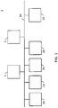
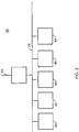
- FIG. 1 illustrates a generic data center 1 comprising a plurality of large scale memory systems 20 that are accessible through a data network 10, and may receive requests for data or for data to be stored from a plurality of servers 5 or network interfaces (not shown) to the Internet, a wide-area network (WAN), or similar communications system.
- each of the large scale memory systems 20 may be comprised of a RAIDed memory system having a RAID controller 30 and a plurality of memory modules 40 in communication with the RAID controller 30.
- Examples of such a memory system may be found in US 11/405,083 , entitled "Interconnection System", where memory modules are in communication with a memory controller, which may be a RAID or tree controller, over a branching tree network, or over a star network, a switched fabric of PCIe links, or the like.
- the RAID controller may allocate strips of a RAID stripe to memory modules 40 in accordance with a protocol.
- the protocol may allocate the data and the redundancy data such that the failure of any single memory module does not cause a loss of data.
- the characteristics of FLASH memory include a substantial asymmetry in the time to read data and to write data to the FLASH memory.
- the write-once-only-before-erase limitation of the NAND FLASH technology also requires occasional erasing of a block of block of the memory, comprising a plurality of pages of data, and the erase operation takes a considerably longer time than that required for an individual write or read operation.
- the excess read latency may be obviated.
- controlling or scheduling the erase or write operations of the memory modules 40 that are used to store a RAID stripe such that only one of the memory modules 40 of the RAID stripe is performing a write or an erase operation at any time permits the reconstruction of the data of the RAID strip by either reading the actual stored data, or by reading less than all of the actual stored data, but including the redundancy (in this case parity) data, and computing the remaining data using an algorithm (in this case exclusive-OR of the strips and the parity strip).
- the data set of the two data sets that is first received may be processed so as to return the stored data to a user, resulting in a low-latency read. This approach to managing a memory is termed "erase hiding" or "write hiding.
- FIG. 3 shows a timing diagram of five memory modules 40 of a memory system 20, each memory module 40 being associated with a same RAID group.
- a period may be allocated for performing erase operations, and a period of time may be allocated for performing write operations.
- the constraint may be that no two of the memory modules 40 may be performing an erase or a write operation at the same time. So, a read operation may be performed immediately on all but one of the memory modules 40 of a RAID group.
- the duration of the period of time during which the erase operation(s) and the write operations(s) are permitted to be performed may be either fixed or variable, providing that the constraint is met.
- the pending erase operations may result in filling an entire epoch for MM1, but may be completed earlier for MM2, depending on work load of each memory module.
- the amount of time occupied by the write operations may use as much of the allocated epoch as is needed.
- pending write operations may be performed during the erase period.
- modules assigned to a RAID group may be located in a single memory system 20, or distributed over a plurality of memory systems 20.
- frame is convenient to describe a plurality of sequential epochs of a RAID group such that each of the modules of the RAID group has been allocated an epoch where erase (which may also include write) operations may be performed.
- the frame may also be a plurality of frames.
- a frame of 10 epochs of time which may be repeated indefinitely (which may represent a 4+1 RAID configuration), which provides both "write” and "erase” hiding.
- the boundaries between the epochs of time for a plurality of memory modules of a RAID group should remain in the same relationship to each other as shown in FIG. 3 . If the frames of different memory modules 40 drift in time with respect to each other, in a relatively short time the erase periods of two or more memory modules will begin to overlap, and the latency performance will degrade. Keeping the memory modules in epoch synchronization may be relatively straightforward within a memory system 20. However, as the scale size of a data center 1 increases to a plurality of memory system20, maintaining the epoch synchronization is more complex. Even within an individual memory system 20, attention to the maintaining alignment between individual memory modules 40 of the RAID group is needed.
- Time may be maintained by counting cycles of an oscillator, where a number of counts equal to that of the oscillator frequency is termed a second.
- accuracy of this measurement depends of the oscillator having the presumed frequency. Often a 10MHz oscillator is used and 10 7 counts represent a second.
- the accuracy of such oscillators in a system may range from ⁇ 50 parts per million (ppm) to several parts per billion (ppb), and may be a function of temperature. If an oscillator having an accuracy of ⁇ 50 ppm were used, two circuits using separate oscillators may differ by 100ppm, and this is 100 usec/s of differential time slippage. Even where highly accurate clocks are used, there is an excessive amount of cumulative time slippage will occur.
- the maintenance of and the measurement of time may be described with reference to an oscillator, a clock, a counter, or the like, however implemented.
- Each particular approach to measuring time, maintaining a clock or the like may be characterized as having a particular accuracy and precision. So, thee terms may be used interchangeably in accordance with conventional practice.
- the long-term accuracy of the measurement of time may be achieved using Cesium beam and Rubidium clocks, used to control the long term drift of a crystal oscillator, or the like.
- Indirect methods such as using the inherently highly accurate time base of the global positioning system (GPS) may also be used. GPS-type methods are useful when units are dispersed over a large geographical area, as the same time value is available to all of the units without the need for another time transfer mechanism.
- GPS global positioning system
- the difference in apparent time between two circuits may be 10 ⁇ sec, and this time is cumulative, so that after 10 seconds, the clocks will differ by 1 msec, which is ten percent of the epoch time.
- a more accurate clock could be used; however, increased clock accuracy is characterized by increasing part cost, size, and power consumption. In a large memory system, where there may be 50 or more separate oscillators , this can represent a substantial design impact.
- a clock frequency is distributed to each of the memory modules 40 of the memory system 20, but this may lead to other design constraints and reliability issues. Whether a distributed clock or multiple clocks are used, the situation is exacerbated when a plurality of memory systems 20 need to be coordinated.
- ⁇ max ⁇ ⁇ ⁇ T ⁇ 10 ⁇ 3 ⁇ sec
- the operation of a plurality of memory systems 20 in a data center, or portion thereof are operated as essentially independent memory systems, being interconnected by, for example, an Ethernet, a Fiber Channel, a Infiniband network, or the like 10, with the interaction between each of the memory systems 20 and the remainder of the environment being effected through standard interface protocols, such as iSCSI, TCP/IP, or the like.
- standard interface protocols such as iSCSI, TCP/IP, or the like.
- the internal timing of the operations of the memory systems are isolated from each other and the environment at the time scale of the operation of the interface, which may be substantially greater than the time scale of operations that may be performed within the memory system 20.
- RAID such as described above, may be performed within the domain of a memory system 20, or even a subset of the memory system 20.
- a higher level RAID architecture may be desired so that the failure of a single memory system 20, a rack enclosure having a plurality of memory systems 20, or the like, does not result in the loss of data. That is, strips of a stripe of data may be distributed across a plurality of memory systems 20, with each of the memory systems 20 performing the function of a memory module 40.
- a system having this architecture and where the operations of a plurality of memory systems 20 (sometimes called a "chassis") are coordinated so that data received by an interface to a memory system 20 may be distributed across a plurality of memory systems 20 for data protection purposes.
- the memory modules 40 of a single memory system 20 may have time base drifts between them, and this situation extends to each of the memory systems 20 of a plurality of memory systems 20.
- a single clock source may be distributed to each of the memory systems 20 so that the same time base is used by each memory system 20, and the same clock frequency may be distributed internally to the memory system 20 so that the same time base is used by each of the memory modules 40.
- the precision of synchronization of the start of a frame is related to the duration of the frame and the amount of latency or other overhead associated with lack of complete synchronization.
- the epoch is 10 msec and the frame is 10 epochs
- a cumulative error of ⁇ 5 ⁇ sec would have accumulated, or a peak error of 10 ⁇ sec.
- This error is 0.1 percent of the epoch, and allowing such a tolerance would not cause a noticeable degradation of the latency.
- the memory modules 40 may have relatively imprecise computer grade oscillators maintaining a local time and this time may be periodically corrected by receiving a signal from a higher level of the system.
- the synchronization of the epochs and frames may be performed in a time period comparable with the duration of a frame.
- memory systems 20 may maintain their own clock and time, and synchronization between memory systems 20 may be performed on a periodic basis, which may be one or more frame durations. In an example, such a period may be 1 second. Since the clock of a memory system 20 may be selected to be more accurate than that of each memory module 40 of the memory system 20, a longer period may be satisfactory. Such synchronization of between memory systems 20 provides for the replacement or reset of an entire memory system without interruption of service.
- a 1 second synchronization period is compatible with many pulse sources, including the output from a Global Positioning System (GPS) receiver.
- GPS Global Positioning System
- the time of each 1 second output pulse bears a known relationship to the global time system (UTC) and would occur at the same instant of time at widely separated sites, obviating the need for transmitting a precision time signal outside of a local domain.
- UTC global time system
- the approach to synchronizing the memory modules 40 within a memory system 20 may be different than that used for synchronizing a plurality of memory systems 20, and depend on the architecture of each, and convenience of various interconnection protocols, including the ability to transmit the synchronization signal over a path that may be shared with other functions, such as data transmission.
- the local time base once synchronized, drifts slowly, ⁇ max , per frame. If a synchronization signal is received once per frame, the maximum expected error is ⁇ max per frame. So, the local time is within ⁇ max of being correct with respect to the global time base.
- the measured error, ⁇ may be used to correct the local time base on a discrete or continuous basis, in accordance with an algorithm.
- an error condition may be considered to exist if the measured error between the time bases exceeds a specified number of standard deviations of the value of the maximum offset error (except, for example, after a reset). So, if the error exceeds a limit, any individual synchronization signal may be, for example, ignored.
- a plurality of synchronization signals having a closely similar error measurement error may be taken as representing the global time base.
- a characteristic of oscillators is that the signal has a noise spectrum that has a random component and there is also a secular component, the offset ⁇ , which may be termed the clock bias.
- the bias changes very slowly as a result of crystal ageing and somewhat more rapidly due to changes in the temperature of operation of the crystal.
- each of the bias terms has a very slow rate of change with respect to a frame time. So, successive offsets between the local time and the global time as measured at a particular memory module 40 are expected to be slowly changing.
- Each memory module 40, having a different clock module will have a specific error at any time and may be either positive or negative with respect to the global time.
- Each epoch of a frame at a memory module 40 may be allocated to one of an erase interval, one or more write intervals or to read operations.
- the erase hiding or write hiding criteria may established such that, for example, no two memory modules 40 in a RAID group are performing a write or erase operation at the same time, in the RAID type is that of a single parity strip.
- the assignment of a particular frame format to a memory module 40 may be made by a message sent, for example, from the local RAID controller, or by a protocol that depends on the physical location of the memory module 40 in a memory system 20, or some other method to accomplish the same result.
- the communications between portions of the data center needed to establish the synchronization may use different protocols at different levels of the architecture.
- the memory systems 20, which may have, for example, Ethernet interfaces may be synchronized by using an industry standard protocol such as IEEE 1588.
- the master for such a system may be a system host board (SHB), which may be further synchronized to a GPS receiver or GPS disciplined oscillator (see FIG. 4 ).
- SHB system host board
- the synchronization signal may be used to control the frame interval duration and to generate internal messages, pulses or the like so as to communicate the start of a frame to each of the memory modules 40 that may need such signals.
- the signals may be distributed directly or through the RAID controller 30 or other path, whether in-band or out-of band.
- GPS is representative of several orbiting-satellite-related global time systems that are in use or development, including GLONASS, and systems being developed by the European Union and the People's Republic of China.
- GLONASS Globalstar Satellite System
- NTP Network Time Protocol
- one of the memory systems 20 of a group of memory systems 20 may act as the master timekeeper and distribute synchronization messages to the other memory systems of the group of memory systems.
- the memory systems 20 are connected by, for example, an Ethernet, provisions can be made for another of the memory systems 20 of the group of memory systems 20 to act as a redundant timekeeper.
- groups of memory systems may communicate with each other so as to maintain epoch synchronization over a larger storage domain.
- the synchronization of operations may be performed in a hierarchical manner, which may be, for example, a tree-like distribution approach, or a single top-level synchronization module may distribute the synchronization signals directly to a low-level memory module.
- a hierarchical manner which may be, for example, a tree-like distribution approach, or a single top-level synchronization module may distribute the synchronization signals directly to a low-level memory module.
- Intermediate cases are also useful and intended to be within the scope of this disclosure.
- the memory module 40 has a local crystal and keeps a local time base that was originally synchronized to the next higher level time base in the system. This may have occurred during a reset or initialization event.
- the local clock and the higher clock will slowly drift with respect to each other in either a positive or a negative time sense, depending on the specific offset bias of each oscillator.
- the local time is running faster than the higher time; where the ⁇ is negative, the local time is running slower than the higher time. Consequently, the local time should be decreased by ⁇ (taking account of the sign of ⁇ ) to bring the two clocks into coincidence.
- This method does not correct the actual clock of the memory module 40, but prevents the time bases from diverging. Since ⁇ is relatively constant over a period of time (the differential bias of the oscillators being very slowly varying as compared with the frame time), the value of ⁇ used
- the error ⁇ may be used to control the frequency of the oscillator of the memory module. This approach drives the offset to zero and may be a frequency locked loop.
- Clock time is kept by counting the number of cycles of an oscillator of a known frequency, and as we have described, an error in the clock frequency results in an error in computing the time, and this error is cumulative. It is also the case that an interval of time, such as an epoch or frame, determined by counting the number of cycles of an oscillator is shorter or longer than the actual time interval depending on whether the oscillator frequency is greater than or less than the expect frequency, respectively.
- the time would be correct, providing that the number of counts of the clock are used to determine the time interval (e.g., 100 msec, 1 sec) is adjusted by ⁇ . Providing that the number of counts is adjusted in this manner, both the time at the local memory module 40 and the duration of the epoch or frame at the local memory module 40 would be the same for all of the memory modules 40.
- the initial value of ⁇ at each module, and the number of counts used to measure the interval would differ for each module depending of the specific frequency offset between the local oscillator and the higher level oscillator frequency.
- the sync pulse or command from the higher level of the system defines, for example, an epoch or a frame
- adjusting the number of counts of the local clock defining the local epoch or frame means that the duration of the local frame is changed so as to closely approximate that of the higher level frame.
- the value of ⁇ would be essentially zero. That is, the two intervals would be the same. So, the number of local clock pulses that are used to define the local frame would not change from the previous measurement. Over a long period of time, the difference between the local clock and the higher level clock may be expected to change due to ageing of the local clock, temperature changes or other phenomenon known to persons of skill in the art of timekeeping. When these changes occur, the value of ⁇ would deviate from nominally zero, and the number of clock pulses defining an interval at the local memory module 40 would change accordingly.
- values of ⁇ are close to zero and one may reduce any jitter in the correction by averaging a plurality of sequential measurements. This may conveniently be done, for example, in an exponential averaging filter so that the changes necessary are applied in a smoothed but timely manner.
- the timekeeping capability of the local memory module 40 is not significantly affected when the time sync process may be interrupted. This might occur when a redundant component is replaced and the source of the clock is changed. Whatever the cause of a missing sync, the time interval error had already been adjusted to nominally zero by the altering of the number of counts in the interval and, at least for some period of time, the error will not significantly cumulate.
- time intervals in the memory module 40 may also depend on this time and the epoch time may be accurately computed as a percentage of the number of counts in the interval. Moreover, if the overall duration of the epoch time durations of a frame may be set such that the frame completes slightly before the actual frame time, the adjustment of the clock counts may be conveniently performed, and the next frame started on time.
- This discussion is intended to indicate that there are a number of methods of maintaining time within a large distributed memory system or data center such that the operation of a RAID group, or other operations that benefit from time synchronization may be effectively coordinated.
- the epoch and frame times may be variable and be controlled using supervisory messages, as the underlying clock times are now coordinated.
- a plurality of 100 msec frames could be used so that the sync time is 1 second.
- GPS global positioning system
- UCT Universal Coordinated Time
Landscapes
- Engineering & Computer Science (AREA)
- Theoretical Computer Science (AREA)
- Physics & Mathematics (AREA)
- General Engineering & Computer Science (AREA)
- General Physics & Mathematics (AREA)
- Human Computer Interaction (AREA)
- Quality & Reliability (AREA)
- Techniques For Improving Reliability Of Storages (AREA)
Claims (1)
- Speichersystem (1), umfassend:eine Mehrzahl von Speichersubsystemen (20), die durch ein Datennetzwerk (10) verbunden sind,wobei jedes Speichersubsystem eine Mehrzahl von Speichermodulen (40) in Verbindung mit einer Speichersteuerung umfasst;wobei die Mehrzahl von Speichersubsystemen konfiguriert ist, um von einem der Mehrzahl von Speichersubsystemen in einer RAID-Gruppe empfangene Daten zu speichern;Speichermodule, ausgewählt unter zwei oder mehr Speichersubsystemen der Mehrzahl von Speichersubsystemen, wobei die ausgewählten Speichermodule der RAID-Gruppe zugeordnet sind,wobei Speichermodule der sich über die zwei oder mehr Speichersubsysteme erstreckenden RAID-Gruppe mit Zeitrahmen verknüpft sind, die eine Mehrzahl von Zeitepochen umfassen, wobei der Beginn jeder Epoche für ein Speichermodul der RAID-Gruppe so gesteuert wird, dass entweder ein Lesevorgang oder ein Schreib- oder Löschvorgang vom Speichermodul in einer Epoche für die RAID-Gruppe durchgeführt wird, und die Lösch- oder Schreibvorgänge in einer anderen Epoche derselben RAID-Gruppe so geplant werden, dass keine zwei Speichermodule der RAID-Gruppe in derselben Epoche einen Schreib- oder Löschvorgang durchführen, so dass die in den Modulen der RAID-Gruppe gespeicherten Daten ohne einen Konflikt zwischen Lesevorgängen und Lösch- oder Schreibvorgängen gelesen werden können; undwobei jedes der Mehrzahl von Speichersystemen ein separates Zeitbestimmungsmodul aufweist und die Zeitbestimmungsmodule der Mehrzahl von Speichersystemen so miteinander synchronisiert sind, dass der Konflikt zwischen Leseoperationen und Lösch- oder Schreiboperationen vermieden wird.
Applications Claiming Priority (2)
| Application Number | Priority Date | Filing Date | Title |
|---|---|---|---|
| US201261667660P | 2012-07-03 | 2012-07-03 | |
| PCT/US2013/049067 WO2014008261A1 (en) | 2012-07-03 | 2013-07-02 | Synchronization of a dispersed raid group |
Publications (4)
| Publication Number | Publication Date |
|---|---|
| EP2870538A1 EP2870538A1 (de) | 2015-05-13 |
| EP2870538A4 EP2870538A4 (de) | 2016-02-24 |
| EP2870538B1 true EP2870538B1 (de) | 2019-10-16 |
| EP2870538B8 EP2870538B8 (de) | 2019-11-27 |
Family
ID=49879410
Family Applications (1)
| Application Number | Title | Priority Date | Filing Date |
|---|---|---|---|
| EP13813635.3A Active EP2870538B8 (de) | 2012-07-03 | 2013-07-02 | Synchronisation einer dispergierten raid-gruppe |
Country Status (4)
| Country | Link |
|---|---|
| US (1) | US9361047B2 (de) |
| EP (1) | EP2870538B8 (de) |
| KR (1) | KR102090090B1 (de) |
| WO (1) | WO2014008261A1 (de) |
Families Citing this family (13)
| Publication number | Priority date | Publication date | Assignee | Title |
|---|---|---|---|---|
| US20150026505A1 (en) * | 2013-07-17 | 2015-01-22 | Kabushiki Kaisha Toshiba | Storage device, storage system, and background processing execution method |
| KR102330391B1 (ko) | 2014-09-11 | 2021-11-24 | 삼성전자주식회사 | 저장 장치 및 그것을 포함하는 데이터 저장 시스템의 가비지 컬렉션 방법 |
| US9806876B2 (en) | 2015-03-30 | 2017-10-31 | Telefonaktiebolaget Lm Ericsson (Publ) | Method and apparatus for compensating synchronization timing in a distributed timing network |
| US9804787B2 (en) | 2015-11-03 | 2017-10-31 | Samsung Electronics Co., Ltd. | Mitigating GC effect in a raid configuration |
| US10467195B2 (en) * | 2016-09-06 | 2019-11-05 | Samsung Electronics Co., Ltd. | Adaptive caching replacement manager with dynamic updating granulates and partitions for shared flash-based storage system |
| US10455045B2 (en) | 2016-09-06 | 2019-10-22 | Samsung Electronics Co., Ltd. | Automatic data replica manager in distributed caching and data processing systems |
| CZ2016826A3 (cs) | 2016-12-22 | 2018-07-04 | Contipro A.S. | Léčivý prostředek s nosičem na bázi hyaluronanu a/nebo jeho derivátů, způsob výroby a použití |
| CN107066419B (zh) * | 2017-03-23 | 2023-08-11 | 桂林理工大学 | 可扩展的自适应n×n通道数据通信系统 |
| US10068663B1 (en) * | 2017-05-30 | 2018-09-04 | Seagate Technology Llc | Data storage device with rewriteable in-place memory |
| KR102369402B1 (ko) | 2017-09-20 | 2022-03-02 | 삼성전자주식회사 | 스토리지 장치, 이의 동작 방법 및 스토리지 장치를 포함하는 스토리지 시스템 |
| US11633673B2 (en) * | 2018-05-17 | 2023-04-25 | Universal City Studios Llc | Modular amusement park systems and methods |
| DE112018007716B4 (de) * | 2018-07-11 | 2022-05-12 | Mitsubishi Electric Corporation | Drahtloses Kommunikationssystem, drahtloses Kommunikationsverfahren und Speichermedium zum Speichern eines Programms zum Steuern des Systems |
| US10866144B2 (en) * | 2018-08-24 | 2020-12-15 | Siemens Industry, Inc. | Branch circuit thermal monitoring system for continuous temperature monitoring by directly applied sensors |
Family Cites Families (12)
| Publication number | Priority date | Publication date | Assignee | Title |
|---|---|---|---|---|
| US7289541B2 (en) * | 2002-12-04 | 2007-10-30 | Raytheon Company | Method for locating and tracking communication units in a synchronous wireless communication system |
| US8200887B2 (en) | 2007-03-29 | 2012-06-12 | Violin Memory, Inc. | Memory management system and method |
| US9632870B2 (en) * | 2007-03-29 | 2017-04-25 | Violin Memory, Inc. | Memory system with multiple striping of raid groups and method for performing the same |
| KR101481162B1 (ko) * | 2007-12-04 | 2015-01-09 | 엘지전자 주식회사 | Cpu 및 메모리의 클럭 주파수 동기화 방법 및 이를이용한 장치 |
| KR100898658B1 (ko) * | 2007-12-28 | 2009-05-22 | 엘지노텔 주식회사 | 인터넷 시각 동기화 프로토콜을 이용한 통신 단말기 시스템클럭의 보정 방법 |
| US20100205355A1 (en) * | 2009-02-11 | 2010-08-12 | Memory Experts International Inc. | Multiplexing secure digital memory |
| EP4361815A3 (de) * | 2009-10-09 | 2024-06-19 | Violin Systems LLC | Speichersystem mit multiple-striping von raid-gruppen und verfahren zur durchführung davon |
| US8504767B2 (en) * | 2010-04-20 | 2013-08-06 | Taejin Info Tech Co., Ltd. | Raid controlled semiconductor storage device |
| US8417989B2 (en) | 2010-10-15 | 2013-04-09 | Lsi Corporation | Method and system for extra redundancy in a raid system |
| KR101855435B1 (ko) | 2010-11-15 | 2018-05-08 | 삼성전자주식회사 | 최대 검증-시간을 조절할 수 있는 비휘발성 메모리 장치, 이의 동작 방법, 및 이를 포함하는 메모리 시스템 |
| US9335939B2 (en) * | 2011-07-12 | 2016-05-10 | Violin Memory Inc. | RAIDed memory system |
| US9513845B2 (en) * | 2012-03-30 | 2016-12-06 | Violin Memory Inc. | Memory module virtualization |
-
2013
- 2013-07-02 EP EP13813635.3A patent/EP2870538B8/de active Active
- 2013-07-02 US US13/933,310 patent/US9361047B2/en active Active
- 2013-07-02 WO PCT/US2013/049067 patent/WO2014008261A1/en not_active Ceased
- 2013-07-02 KR KR1020157002929A patent/KR102090090B1/ko active Active
Non-Patent Citations (1)
| Title |
|---|
| None * |
Also Published As
| Publication number | Publication date |
|---|---|
| EP2870538A1 (de) | 2015-05-13 |
| EP2870538A4 (de) | 2016-02-24 |
| EP2870538B8 (de) | 2019-11-27 |
| KR102090090B1 (ko) | 2020-03-17 |
| US20140013048A1 (en) | 2014-01-09 |
| KR20150037985A (ko) | 2015-04-08 |
| US9361047B2 (en) | 2016-06-07 |
| WO2014008261A1 (en) | 2014-01-09 |
Similar Documents
| Publication | Publication Date | Title |
|---|---|---|
| EP2870538B1 (de) | Synchronisation einer dispergierten raid-gruppe | |
| US20240143560A1 (en) | Systems and Methods for Increasing Database Access Concurrency | |
| US20250086200A1 (en) | Pipelining Paxos State Machines | |
| US7644249B2 (en) | Method of designing storage system | |
| JP6144819B2 (ja) | 不揮発性メモリシステムにおける同期ミラーリング | |
| US9348761B1 (en) | Weighted-value consistent hashing for balancing device wear | |
| EP4459475A2 (de) | Dynamische konfiguration eines speichersystems zur ermöglichung von unabhängiger skalierung von ressourcen | |
| US10903924B2 (en) | Setting primary reference time of server time protocol facility of a coordinated timing network to a precision-time-protocol source | |
| CN107017959A (zh) | 一种利用对时提高守时精度的方法及装置 | |
| EP2856356A2 (de) | Systeme und verfahren zur erhöhung gleichzeitiger datenbankzugriffe mithilfe teilchenförmiger zeitmarken | |
| US10503426B2 (en) | Efficient space allocation in gathered-write backend change volumes | |
| US11182077B1 (en) | Systems, devices and methods using a solid state device as a caching medium with an SSD filtering or SSD pre-fetch algorithm | |
| EP3213456B1 (de) | Verfahren zur synchronisierung eines host-rechners mit verschiedenen externen vorrichtungen | |
| WO2020160933A1 (en) | Facilitating precision time protocol use in a coordinated timing network | |
| US10719399B2 (en) | System combining efficient reliable storage and deduplication | |
| US9104364B2 (en) | Generation and distribution of steered time interval pulse to a plurality of hardware components of the computing system | |
| US10958727B2 (en) | Facilitating precision time protocol use in a coordinated timing network | |
| US20210247913A1 (en) | Storage apparatus and data processing method for storage apparatus | |
| US11853114B1 (en) | Virtualized hardware clocks for providing highly accurate time information in hosted machine instances | |
| US6665809B1 (en) | Digital frequency correction | |
| US10560523B1 (en) | Converting and synchronizing system times |
Legal Events
| Date | Code | Title | Description |
|---|---|---|---|
| PUAI | Public reference made under article 153(3) epc to a published international application that has entered the european phase |
Free format text: ORIGINAL CODE: 0009012 |
|
| 17P | Request for examination filed |
Effective date: 20150130 |
|
| AK | Designated contracting states |
Kind code of ref document: A1 Designated state(s): AL AT BE BG CH CY CZ DE DK EE ES FI FR GB GR HR HU IE IS IT LI LT LU LV MC MK MT NL NO PL PT RO RS SE SI SK SM TR |
|
| AX | Request for extension of the european patent |
Extension state: BA ME |
|
| DAX | Request for extension of the european patent (deleted) | ||
| REG | Reference to a national code |
Ref country code: DE Ref legal event code: R079 Ref document number: 602013061821 Country of ref document: DE Free format text: PREVIOUS MAIN CLASS: G06F0013140000 Ipc: G06F0011100000 |
|
| RA4 | Supplementary search report drawn up and despatched (corrected) |
Effective date: 20160121 |
|
| RIC1 | Information provided on ipc code assigned before grant |
Ipc: G06F 12/00 20060101ALI20160115BHEP Ipc: G06F 11/10 20060101AFI20160115BHEP |
|
| GRAP | Despatch of communication of intention to grant a patent |
Free format text: ORIGINAL CODE: EPIDOSNIGR1 |
|
| STAA | Information on the status of an ep patent application or granted ep patent |
Free format text: STATUS: GRANT OF PATENT IS INTENDED |
|
| INTG | Intention to grant announced |
Effective date: 20180705 |
|
| GRAJ | Information related to disapproval of communication of intention to grant by the applicant or resumption of examination proceedings by the epo deleted |
Free format text: ORIGINAL CODE: EPIDOSDIGR1 |
|
| STAA | Information on the status of an ep patent application or granted ep patent |
Free format text: STATUS: REQUEST FOR EXAMINATION WAS MADE |
|
| INTC | Intention to grant announced (deleted) | ||
| GRAP | Despatch of communication of intention to grant a patent |
Free format text: ORIGINAL CODE: EPIDOSNIGR1 |
|
| STAA | Information on the status of an ep patent application or granted ep patent |
Free format text: STATUS: GRANT OF PATENT IS INTENDED |
|
| INTG | Intention to grant announced |
Effective date: 20190514 |
|
| GRAS | Grant fee paid |
Free format text: ORIGINAL CODE: EPIDOSNIGR3 |
|
| GRAA | (expected) grant |
Free format text: ORIGINAL CODE: 0009210 |
|
| STAA | Information on the status of an ep patent application or granted ep patent |
Free format text: STATUS: THE PATENT HAS BEEN GRANTED |
|
| AK | Designated contracting states |
Kind code of ref document: B1 Designated state(s): AL AT BE BG CH CY CZ DE DK EE ES FI FR GB GR HR HU IE IS IT LI LT LU LV MC MK MT NL NO PL PT RO RS SE SI SK SM TR |
|
| REG | Reference to a national code |
Ref country code: GB Ref legal event code: FG4D |
|
| REG | Reference to a national code |
Ref country code: CH Ref legal event code: EP Ref country code: CH Ref legal event code: PK Free format text: BERICHTIGUNG B8 |
|
| REG | Reference to a national code |
Ref country code: DE Ref legal event code: R096 Ref document number: 602013061821 Country of ref document: DE |
|
| RAP2 | Party data changed (patent owner data changed or rights of a patent transferred) |
Owner name: VIOLIN SYSTEMS LLC |
|
| REG | Reference to a national code |
Ref country code: IE Ref legal event code: FG4D |
|
| REG | Reference to a national code |
Ref country code: AT Ref legal event code: REF Ref document number: 1191960 Country of ref document: AT Kind code of ref document: T Effective date: 20191115 |
|
| REG | Reference to a national code |
Ref country code: NL Ref legal event code: MP Effective date: 20191016 |
|
| REG | Reference to a national code |
Ref country code: LT Ref legal event code: MG4D |
|
| REG | Reference to a national code |
Ref country code: AT Ref legal event code: MK05 Ref document number: 1191960 Country of ref document: AT Kind code of ref document: T Effective date: 20191016 |
|
| PG25 | Lapsed in a contracting state [announced via postgrant information from national office to epo] |
Ref country code: ES Free format text: LAPSE BECAUSE OF FAILURE TO SUBMIT A TRANSLATION OF THE DESCRIPTION OR TO PAY THE FEE WITHIN THE PRESCRIBED TIME-LIMIT Effective date: 20191016 Ref country code: NL Free format text: LAPSE BECAUSE OF FAILURE TO SUBMIT A TRANSLATION OF THE DESCRIPTION OR TO PAY THE FEE WITHIN THE PRESCRIBED TIME-LIMIT Effective date: 20191016 Ref country code: SE Free format text: LAPSE BECAUSE OF FAILURE TO SUBMIT A TRANSLATION OF THE DESCRIPTION OR TO PAY THE FEE WITHIN THE PRESCRIBED TIME-LIMIT Effective date: 20191016 Ref country code: LV Free format text: LAPSE BECAUSE OF FAILURE TO SUBMIT A TRANSLATION OF THE DESCRIPTION OR TO PAY THE FEE WITHIN THE PRESCRIBED TIME-LIMIT Effective date: 20191016 Ref country code: PL Free format text: LAPSE BECAUSE OF FAILURE TO SUBMIT A TRANSLATION OF THE DESCRIPTION OR TO PAY THE FEE WITHIN THE PRESCRIBED TIME-LIMIT Effective date: 20191016 Ref country code: LT Free format text: LAPSE BECAUSE OF FAILURE TO SUBMIT A TRANSLATION OF THE DESCRIPTION OR TO PAY THE FEE WITHIN THE PRESCRIBED TIME-LIMIT Effective date: 20191016 Ref country code: NO Free format text: LAPSE BECAUSE OF FAILURE TO SUBMIT A TRANSLATION OF THE DESCRIPTION OR TO PAY THE FEE WITHIN THE PRESCRIBED TIME-LIMIT Effective date: 20200116 Ref country code: GR Free format text: LAPSE BECAUSE OF FAILURE TO SUBMIT A TRANSLATION OF THE DESCRIPTION OR TO PAY THE FEE WITHIN THE PRESCRIBED TIME-LIMIT Effective date: 20200117 Ref country code: BG Free format text: LAPSE BECAUSE OF FAILURE TO SUBMIT A TRANSLATION OF THE DESCRIPTION OR TO PAY THE FEE WITHIN THE PRESCRIBED TIME-LIMIT Effective date: 20200116 Ref country code: FI Free format text: LAPSE BECAUSE OF FAILURE TO SUBMIT A TRANSLATION OF THE DESCRIPTION OR TO PAY THE FEE WITHIN THE PRESCRIBED TIME-LIMIT Effective date: 20191016 Ref country code: PT Free format text: LAPSE BECAUSE OF FAILURE TO SUBMIT A TRANSLATION OF THE DESCRIPTION OR TO PAY THE FEE WITHIN THE PRESCRIBED TIME-LIMIT Effective date: 20200217 Ref country code: AT Free format text: LAPSE BECAUSE OF FAILURE TO SUBMIT A TRANSLATION OF THE DESCRIPTION OR TO PAY THE FEE WITHIN THE PRESCRIBED TIME-LIMIT Effective date: 20191016 |
|
| PG25 | Lapsed in a contracting state [announced via postgrant information from national office to epo] |
Ref country code: HR Free format text: LAPSE BECAUSE OF FAILURE TO SUBMIT A TRANSLATION OF THE DESCRIPTION OR TO PAY THE FEE WITHIN THE PRESCRIBED TIME-LIMIT Effective date: 20191016 Ref country code: RS Free format text: LAPSE BECAUSE OF FAILURE TO SUBMIT A TRANSLATION OF THE DESCRIPTION OR TO PAY THE FEE WITHIN THE PRESCRIBED TIME-LIMIT Effective date: 20191016 Ref country code: IS Free format text: LAPSE BECAUSE OF FAILURE TO SUBMIT A TRANSLATION OF THE DESCRIPTION OR TO PAY THE FEE WITHIN THE PRESCRIBED TIME-LIMIT Effective date: 20200224 |
|
| PG25 | Lapsed in a contracting state [announced via postgrant information from national office to epo] |
Ref country code: AL Free format text: LAPSE BECAUSE OF FAILURE TO SUBMIT A TRANSLATION OF THE DESCRIPTION OR TO PAY THE FEE WITHIN THE PRESCRIBED TIME-LIMIT Effective date: 20191016 |
|
| REG | Reference to a national code |
Ref country code: DE Ref legal event code: R097 Ref document number: 602013061821 Country of ref document: DE |
|
| PG2D | Information on lapse in contracting state deleted |
Ref country code: IS |
|
| PG25 | Lapsed in a contracting state [announced via postgrant information from national office to epo] |
Ref country code: RO Free format text: LAPSE BECAUSE OF FAILURE TO SUBMIT A TRANSLATION OF THE DESCRIPTION OR TO PAY THE FEE WITHIN THE PRESCRIBED TIME-LIMIT Effective date: 20191016 Ref country code: EE Free format text: LAPSE BECAUSE OF FAILURE TO SUBMIT A TRANSLATION OF THE DESCRIPTION OR TO PAY THE FEE WITHIN THE PRESCRIBED TIME-LIMIT Effective date: 20191016 Ref country code: DK Free format text: LAPSE BECAUSE OF FAILURE TO SUBMIT A TRANSLATION OF THE DESCRIPTION OR TO PAY THE FEE WITHIN THE PRESCRIBED TIME-LIMIT Effective date: 20191016 Ref country code: CZ Free format text: LAPSE BECAUSE OF FAILURE TO SUBMIT A TRANSLATION OF THE DESCRIPTION OR TO PAY THE FEE WITHIN THE PRESCRIBED TIME-LIMIT Effective date: 20191016 Ref country code: IS Free format text: LAPSE BECAUSE OF FAILURE TO SUBMIT A TRANSLATION OF THE DESCRIPTION OR TO PAY THE FEE WITHIN THE PRESCRIBED TIME-LIMIT Effective date: 20200216 |
|
| PLBE | No opposition filed within time limit |
Free format text: ORIGINAL CODE: 0009261 |
|
| STAA | Information on the status of an ep patent application or granted ep patent |
Free format text: STATUS: NO OPPOSITION FILED WITHIN TIME LIMIT |
|
| PG25 | Lapsed in a contracting state [announced via postgrant information from national office to epo] |
Ref country code: SK Free format text: LAPSE BECAUSE OF FAILURE TO SUBMIT A TRANSLATION OF THE DESCRIPTION OR TO PAY THE FEE WITHIN THE PRESCRIBED TIME-LIMIT Effective date: 20191016 Ref country code: IT Free format text: LAPSE BECAUSE OF FAILURE TO SUBMIT A TRANSLATION OF THE DESCRIPTION OR TO PAY THE FEE WITHIN THE PRESCRIBED TIME-LIMIT Effective date: 20191016 Ref country code: SM Free format text: LAPSE BECAUSE OF FAILURE TO SUBMIT A TRANSLATION OF THE DESCRIPTION OR TO PAY THE FEE WITHIN THE PRESCRIBED TIME-LIMIT Effective date: 20191016 |
|
| 26N | No opposition filed |
Effective date: 20200717 |
|
| PG25 | Lapsed in a contracting state [announced via postgrant information from national office to epo] |
Ref country code: SI Free format text: LAPSE BECAUSE OF FAILURE TO SUBMIT A TRANSLATION OF THE DESCRIPTION OR TO PAY THE FEE WITHIN THE PRESCRIBED TIME-LIMIT Effective date: 20191016 |
|
| PG25 | Lapsed in a contracting state [announced via postgrant information from national office to epo] |
Ref country code: MC Free format text: LAPSE BECAUSE OF FAILURE TO SUBMIT A TRANSLATION OF THE DESCRIPTION OR TO PAY THE FEE WITHIN THE PRESCRIBED TIME-LIMIT Effective date: 20191016 |
|
| REG | Reference to a national code |
Ref country code: CH Ref legal event code: PL |
|
| GBPC | Gb: european patent ceased through non-payment of renewal fee |
Effective date: 20200702 |
|
| REG | Reference to a national code |
Ref country code: BE Ref legal event code: MM Effective date: 20200731 |
|
| PG25 | Lapsed in a contracting state [announced via postgrant information from national office to epo] |
Ref country code: LI Free format text: LAPSE BECAUSE OF NON-PAYMENT OF DUE FEES Effective date: 20200731 Ref country code: GB Free format text: LAPSE BECAUSE OF NON-PAYMENT OF DUE FEES Effective date: 20200702 Ref country code: IE Free format text: LAPSE BECAUSE OF NON-PAYMENT OF DUE FEES Effective date: 20200702 Ref country code: CH Free format text: LAPSE BECAUSE OF NON-PAYMENT OF DUE FEES Effective date: 20200731 Ref country code: LU Free format text: LAPSE BECAUSE OF NON-PAYMENT OF DUE FEES Effective date: 20200702 Ref country code: FR Free format text: LAPSE BECAUSE OF NON-PAYMENT OF DUE FEES Effective date: 20200731 |
|
| PG25 | Lapsed in a contracting state [announced via postgrant information from national office to epo] |
Ref country code: BE Free format text: LAPSE BECAUSE OF NON-PAYMENT OF DUE FEES Effective date: 20200731 |
|
| PG25 | Lapsed in a contracting state [announced via postgrant information from national office to epo] |
Ref country code: TR Free format text: LAPSE BECAUSE OF FAILURE TO SUBMIT A TRANSLATION OF THE DESCRIPTION OR TO PAY THE FEE WITHIN THE PRESCRIBED TIME-LIMIT Effective date: 20191016 Ref country code: MT Free format text: LAPSE BECAUSE OF FAILURE TO SUBMIT A TRANSLATION OF THE DESCRIPTION OR TO PAY THE FEE WITHIN THE PRESCRIBED TIME-LIMIT Effective date: 20191016 Ref country code: CY Free format text: LAPSE BECAUSE OF FAILURE TO SUBMIT A TRANSLATION OF THE DESCRIPTION OR TO PAY THE FEE WITHIN THE PRESCRIBED TIME-LIMIT Effective date: 20191016 |
|
| PG25 | Lapsed in a contracting state [announced via postgrant information from national office to epo] |
Ref country code: MK Free format text: LAPSE BECAUSE OF FAILURE TO SUBMIT A TRANSLATION OF THE DESCRIPTION OR TO PAY THE FEE WITHIN THE PRESCRIBED TIME-LIMIT Effective date: 20191016 |
|
| PGFP | Annual fee paid to national office [announced via postgrant information from national office to epo] |
Ref country code: DE Payment date: 20250702 Year of fee payment: 13 |