EP2870519B1 - Reconfigurable optical processing system - Google Patents
Reconfigurable optical processing system Download PDFInfo
- Publication number
- EP2870519B1 EP2870519B1 EP13745868.3A EP13745868A EP2870519B1 EP 2870519 B1 EP2870519 B1 EP 2870519B1 EP 13745868 A EP13745868 A EP 13745868A EP 2870519 B1 EP2870519 B1 EP 2870519B1
- Authority
- EP
- European Patent Office
- Prior art keywords
- slm
- optical
- layers
- patterns
- focussing
- Prior art date
- Legal status (The legal status is an assumption and is not a legal conclusion. Google has not performed a legal analysis and makes no representation as to the accuracy of the status listed.)
- Active
Links
Images


Classifications
-
- G—PHYSICS
- G06—COMPUTING OR CALCULATING; COUNTING
- G06E—OPTICAL COMPUTING DEVICES
- G06E3/00—Devices not provided for in group G06E1/00, e.g. for processing analogue or hybrid data
- G06E3/001—Analogue devices in which mathematical operations are carried out with the aid of optical or electro-optical elements
- G06E3/003—Analogue devices in which mathematical operations are carried out with the aid of optical or electro-optical elements forming integrals of products, e.g. Fourier integrals, Laplace integrals, correlation integrals; for analysis or synthesis of functions using orthogonal functions
-
- G—PHYSICS
- G06—COMPUTING OR CALCULATING; COUNTING
- G06E—OPTICAL COMPUTING DEVICES
- G06E3/00—Devices not provided for in group G06E1/00, e.g. for processing analogue or hybrid data
- G06E3/001—Analogue devices in which mathematical operations are carried out with the aid of optical or electro-optical elements
-
- G—PHYSICS
- G02—OPTICS
- G02F—OPTICAL DEVICES OR ARRANGEMENTS FOR THE CONTROL OF LIGHT BY MODIFICATION OF THE OPTICAL PROPERTIES OF THE MEDIA OF THE ELEMENTS INVOLVED THEREIN; NON-LINEAR OPTICS; FREQUENCY-CHANGING OF LIGHT; OPTICAL LOGIC ELEMENTS; OPTICAL ANALOGUE/DIGITAL CONVERTERS
- G02F3/00—Optical logic elements; Optical bistable devices
Definitions
- the invention relates to optical processing. Certain embodiments of the invention concern optical correlation based processing systems, optical pattern recognition systems, optical derivative processing systems, optical equation solving systems, and optical systems for mathematical operations.
- Zeng et al. (Parallel lensless optical correlator based on two phase-only spatial light modulators; Optics Express, vol. 19(13), pp. 12594-12604; DOI:10.1364/OE.19.012594 ) proposed a parallel phase-only lensless optical correlator based on two pieces of liquid crystal on silicon spatial light modulators. Phase Fresnel lens array and specialized grating are implemented to realize multi-channel and multiplexed lensless optical correlators.
- coherent processing systems such as optical correlators, a laser or other coherent source is typically employed to be modulated in either phase or amplitude by one or more spatial light modulator (SLM) devices.
- SLM spatial light modulator
- Optical correlator devices are typically used as optical pattern recognition systems, such as the systems described in EP1546838 (WO2004/029746 ) and EP1420322 ( WO99/31563 ), In a 4f Matched Filter or joint Transform Correlator (JTC) system, the SLM devices are addressed with functions that represent either input or reference patterns (which can be images) and/or filter patterns, usually based upon Fourier transform representations of reference functions/patterns that are to be "matched" to the input function.
- JTC Joint Transform Correlator
- optical derivative processor that is described in EP2137590 ( WO2008/110779 ).
- This employs specific filters to produce derivatives of the input function displayed on an input SLM.
- the optical system It is usual for the optical system to contain one or multiple focussing elements, such as lenses or curved mirrors, in order to produce the Optical Fourier Transform (OFT) of the function represented on the SLM, This is achieved when collimated light is illuminated on an SLM, with the SLM positioned in the front focal plane of the focussing element The OFT is then produced at the rear focal plane of the focussing element, where either a camera or subsequent SLM is positioned.
- Other focussing elements that may be used include static diffractive optical elements, typically in the form of zone plates.
- a camera such as a complementary metal-oxide-semiconductor (CMOS) sensor is typically positioned in the output plane of the optical system to capture the resulting optical intensity distribution, which in the case of an optical correlator system may contain localised correlation intensities denoting the similarity and relative alignment of the input and references functions.
- CMOS complementary metal-oxide-semiconductor
- the camera would capture the resulting derivative of the input function.
- the OFT may be achieved by the optical system shown in Figure 1 where collimated coherent light of wavelength ⁇ (typically laser light) 1 is modulated in phase or amplitude by a Spatial Light Modulator 2 (typically a liquid crystal or electro-mechanical MEMs array).
- ⁇ typically laser light
- Spatial Light Modulator 2 typically a liquid crystal or electro-mechanical MEMs array
- the modulated beam is then passed through a positive converging lens 3, of focal length f and focussed in the back focal plane of the lens, where a detector such as a CMOS array 4 is positioned to capture the intensity of the resulting Fourier transform.
- the OFT may be employed as a direct replacement of the electronic/software-based Fast Fourier Transform (FFT) family of algorithms, offering significant advantages in terms of process time and resolution.
- FFT Fast Fourier Transform
- This process may be used as the basis of a variety of functions.
- the two functions of primary concern in this application are optical correlation (used in pattern recognition, comparison, or analysis) and derivative calculations.
- Figure 2 shows a "4f" optical system that can be used to realise a matched filter or derivative process.
- Figure shows a collimated coherent light 5 of wavelength ⁇ which is modulated by SLM pixel array 6, and then transmitted through lens 7 and focussed on the second SLM pixel array 8, forming the OFT of the function displayed on the first SLM, at the pixels of the second SLM 8, The resulting optical matrix multiplication is then the inverse Fourier transformed by lens 9 and the result is captured at the detector array 10,
- the pattern displayed by the pixels of the first SLM 6 will be the "input scene" g(x,y) and the pattern displayed on the second SLM 8 will represent a version of the Fourier transform of the reference function r(x,y).
- the pattern displayed by the second SLM 8 will be the complex function ( i2 ⁇ uv ) n from equation (3). This may be represented by a combination of phase and amplitude patterns, as described in EP2137590 ( WO2008/110779 ).
- a recognised problem in the physical realisation of such optical systems is the high spatial alignment criteria of the input and filter patterns displayed on the spatial light modulator components, together with the accurate positioning of the other system components, such as lenses and polarisers, etc. These tolerances may be of the order of a few microns, given that the pixel sizes for modern liquid crystal SLMs are of the order of 9 microns.
- Several methodologies have been proposed to alleviate these high tolerances in order to create optical systems that are both practically achievable and resistant to mechanical noise, vibration and shock, as well as gradual misalignment due to such factors as device and environmental temperature variations.
- Such solutions include folding the optical path to reduce both the overall size of the system as well as to reduce the number of discreet components required (such as the joint transform correlator (JTC) embodiment in patent EP2137590 ( WO2008/110779 )) and to replace the positive converging lenses with curved mirrors and static diffraction gratings such as zone plates.
- JTC joint transform correlator
- Extending the use of the spatial light modulator array to incorporate multiple data input patterns and placing the SLM on the same back plane as the detector array has also been proposed.
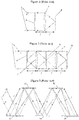
- Figure 3 shows such a folded arrangement, where a 4f-type system is outlined, Collimated coherent light 11 is employed as before as the information medium being transmitted through the optical system.
- the input in SLM 12 and reference/filter SLM 14 are now in the same plane as the detector array 16 and both SLMs are now considered as reflective devices (e.g. pixel arrays mounted upon a plane mirror).
- the lenses of Figure 2 are now replaced by two reflective components 13, and 15, either as diffractive optical elements or positive curved mirrors, of focal length f.
- Equation (4) A form of the NS equations are shown in equation (4) below, in one dimensional form.
- the invention seeks to address at least some of the following problems:
- the present invention provides for an optical processing system according to claim 1, and a corresponding optical processing method according to claim 8. Further aspects of the invention are outlined in the dependent claims. This is particularly advantageous because it allows advantageous configuration and reconfiguration of the elements in order to overcome the drawbacks outlined above. In particular, it allows advantageous alignment of the elements prior to initial use and during use so that the optical processing system may adapt to changing environmental conditions such as the temperature of the device or the temperature surrounding the device. Furthermore, by providing improvements in the alignment, strict tolerances can be adhered to, thus allowing complex, compact and low scale optical processing systems to be configured in order to provide practical solutions to complex processing problems.
- This provides a mechanism to minimise or do away substantially with optical crosstalk noise.
- FIG. 5 shows an embodiment of how the derivative process described above may be realised in accordance with the invention.
- a high resolution pixel array 17 contains several million pixels. Arranged within the array are the input scene g(x,y) 18, first focussing element 19, filter array r(x,y) 20, second focussing element 21 and detector array 22. Each one of the focussing elements 19 and 21 may be a zone plate of the kind shown in Figure 4 .
- the pixel array 17 is preferably reflective and may be mounted on a plane mirror. Opposing the array 17 there may be provided another plane mirror located at a distance of f/2 away from the array such that the distance travelled by the light beam between focussing elements and numerical data represented on the array would match the effective focal length f of the focussing elements 19 and 21.
- the coherent light would then be reflected back and forth, such that each of the data and focusing stages would form a successive optical path resulting in the output distribution being incident on detector 22.
- Spatial/translational alignment is achieved by using a software management algorithm to produce the target optical output on the detector array by a combination of shifting the positions of the numerical data on the pixel array, and changing the focus via modification of the zone plate patterns. Furthermore, beam steering patterns, such as phase ramps or other such patterns are used to steer the beam according to the required optical path.
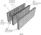
- Figure 6 shows how by replacing the static focusing elements on the optical system, with zone plates such as zone plate 23 displayed on a liquid crystal (or other) SLM, multiple function coherent optical systems may be realised by using opposing high resolution reflective liquid crystal panels such as panel 24 and 25 which may be set to display multiple focussing elements, input functions, reference/derivative filters. Multiple transmissive liquid crystal panels such as panel 26 may be inserted between the opposing reflective liquid crystal panels to add further optical function elements.
- rotational and translational tolerances may be taken care of by way of using the same liquid crystal panel to display the subsequent focussing or data functions.
- Such a system would be dynamic and reprogrammable, whilst being extremely compact and of low size and mass.
- the resulting optical system may be able to perform extremely large processing tasks, such as solving large partial differential equations, for example the Navier-Stokes equations that are the basis of computational fluid dynamics.
- Figure 6 shows the arrangement of two opposing reflective liquid crystal panels 24 and 25 with one single transmissive liquid crystal panel 26. Also shown is a collimated laser beam 27 and the first few interactions of the beam with the focussing and data elements.
- the camera device is not shown but would be positioned wherever the end of the optical system would be positioned. Multiple laser beams could also be employed to produce multiple optical paths through the system.
- a honeycomb-style grid may be inserted between the liquid crystal panels to act as a light trap, with care being taken not to clip the beams.
- Figure 7 shows how the 4f optical system may be extended by adding further functions into the optical path by employing multiple high resolution pixel arrays. For simplicity, the figure only shows the partial voyage of the light beam. Multiple light beams from multiple optical sources may also be used and combined as required through the system. The final detector array, or arrays (not shown) are positioned at the output of the system.
- the method also allows the optical path and functionality to be altered since the data array and optical elements are all dynamically addressable. Multiple optical systems may therefore be realised using the same hardware components, creating a reconfigurable and dynamic arrangement. This may be particularly useful in PDE-type solver systems, where the flow data may be generated and stored temporarily in electronic form, then analysed using the same hardware, reconfigured as an optical pattern recognition system - without the need for any physical realignment or adjustment
- the above embodiment may relate not only to the solving of PDE-type equations and optical pattern recognition, but also more general mathematical operations, in particular matrix multiplication. Other mathematical operations such as addition may be achieved through the use of multiple beams being combined at each state through the optical path.
- Figure 8 shows how the same system described in Figure 6 is dynamically reconfigured into a different optical process by changing the information being addressed. Shown is a single Fourier transform stage which may be used as the 1/f joint Transform Correlator described in EP1546838 .
- the reflective SLM pixel array layer 28 displays an input scene 29 comprising of an input and reference function for comparison.
- a plane mirror facing the SLM array positioned a distance of f/2 from the SLM array, Collimated laser light (which may be collimated and angled using the same zone plate and beam steering method described earlier) illuminates the input scene 29 and is reflected to the plane mirror opposite.
- the captured intensity pattern represents the intensity distribution of the Fourier transform of the input scene, known as the joint Power Spectrum.
- the joint Power Spectrum For a 1/f JTC operation, this is then electronically thresholded/processed and the result undergoes a second Fourier transform to produce the correlation plane.
- This second Fourier transform could use the same system layout described here, replacing the input scene with the processed joint Power Spectrum.
Landscapes
- Physics & Mathematics (AREA)
- Engineering & Computer Science (AREA)
- Theoretical Computer Science (AREA)
- Mathematical Physics (AREA)
- General Physics & Mathematics (AREA)
- Nonlinear Science (AREA)
- Optics & Photonics (AREA)
- Optical Modulation, Optical Deflection, Nonlinear Optics, Optical Demodulation, Optical Logic Elements (AREA)
- Liquid Crystal (AREA)
- Length Measuring Devices By Optical Means (AREA)
Applications Claiming Priority (2)
| Application Number | Priority Date | Filing Date | Title |
|---|---|---|---|
| GBGB1211917.8A GB201211917D0 (en) | 2012-07-04 | 2012-07-04 | Reconfigurable optical processor |
| PCT/GB2013/051778 WO2014087126A1 (en) | 2012-07-04 | 2013-07-04 | Reconfigurable optical processing system |
Publications (2)
| Publication Number | Publication Date |
|---|---|
| EP2870519A1 EP2870519A1 (en) | 2015-05-13 |
| EP2870519B1 true EP2870519B1 (en) | 2022-01-05 |
Family
ID=46721913
Family Applications (1)
| Application Number | Title | Priority Date | Filing Date |
|---|---|---|---|
| EP13745868.3A Active EP2870519B1 (en) | 2012-07-04 | 2013-07-04 | Reconfigurable optical processing system |
Country Status (6)
| Country | Link |
|---|---|
| US (2) | US9594394B2 (enExample) |
| EP (1) | EP2870519B1 (enExample) |
| JP (2) | JP6185996B2 (enExample) |
| CN (1) | CN104508586B (enExample) |
| GB (2) | GB201211917D0 (enExample) |
| WO (1) | WO2014087126A1 (enExample) |
Families Citing this family (24)
| Publication number | Priority date | Publication date | Assignee | Title |
|---|---|---|---|---|
| GB2507469B (en) * | 2012-09-03 | 2020-01-08 | Dualitas Ltd | A multichannel optical device |
| US9939711B1 (en) | 2013-12-31 | 2018-04-10 | Open Portal Enterprises (Ope) | Light based computing apparatus |
| US10545529B1 (en) | 2014-08-11 | 2020-01-28 | OPē, LLC | Optical analog numeric computation device |
| GB201500285D0 (en) * | 2015-01-08 | 2015-02-25 | Optalysys Ltd | Alignment method |
| US9948454B1 (en) | 2015-04-29 | 2018-04-17 | Open Portal Enterprises (Ope) | Symmetric data encryption system and method |
| CN106444213B (zh) * | 2016-08-09 | 2019-08-09 | 北京师范大学 | 一种集成式表面等离激元逻辑电路 |
| US10274989B2 (en) * | 2016-10-13 | 2019-04-30 | Fathom Computing | Wavelength multiplexed matrix-matrix multiplier |
| US10317670B2 (en) | 2017-03-03 | 2019-06-11 | Microsoft Technology Licensing, Llc | MEMS scanning display device |
| US10365709B2 (en) | 2017-03-03 | 2019-07-30 | Microsoft Technology Licensing, Llc | MEMS scanning display device |
| GB2560584B (en) * | 2017-03-17 | 2021-05-19 | Optalysys Ltd | Optical processing systems |
| GB2573171B (en) * | 2018-04-27 | 2021-12-29 | Optalysys Ltd | Optical processing systems |
| CN112424796B (zh) | 2018-06-05 | 2026-01-30 | 光子智能私营科技有限公司 | 光电计算系统 |
| US11507818B2 (en) | 2018-06-05 | 2022-11-22 | Lightelligence PTE. Ltd. | Optoelectronic computing systems |
| US11734556B2 (en) | 2019-01-14 | 2023-08-22 | Lightelligence PTE. Ltd. | Optoelectronic computing systems |
| EP4006690A4 (en) * | 2019-07-24 | 2022-10-26 | Huawei Technologies Co., Ltd. | OPTICAL COMPUTER CHIP, SYSTEM AND DATA PROCESSING TECHNOLOGY |
| TWI758994B (zh) | 2019-12-04 | 2022-03-21 | 新加坡商光子智能私人有限公司 | 光電處理系統 |
| GB2594911B (en) | 2020-01-31 | 2023-08-30 | Optalysys Ltd | Hashing methods and/or systems |
| TWI806042B (zh) | 2020-04-29 | 2023-06-21 | 新加坡商光子智能私人有限公司 | 光電處理設備、系統及方法 |
| CN111624692B (zh) * | 2020-05-20 | 2021-05-04 | 武汉大学 | 基于纳米微腔的光学滤波透镜设计及多波长消色差技术 |
| GB202011415D0 (en) | 2020-07-23 | 2020-09-09 | Optalysys Ltd | Public-key cryptography methods and/or systems |
| GB2598627B (en) | 2020-09-07 | 2024-08-14 | Optalysys Ltd | Optical processing system |
| GB2598757B (en) | 2020-09-10 | 2023-11-15 | Optalysys Ltd | Optical processing systems and methods with feedback loop |
| CN113376928B (zh) * | 2021-06-15 | 2023-04-14 | 上海电子信息职业技术学院 | 一种集成光电子混合比特可逆逻辑门 |
| WO2023276060A1 (ja) * | 2021-06-30 | 2023-01-05 | 株式会社フジクラ | 光演算装置及び光演算方法 |
Family Cites Families (14)
| Publication number | Priority date | Publication date | Assignee | Title |
|---|---|---|---|---|
| JPH04328726A (ja) * | 1991-04-30 | 1992-11-17 | Ricoh Co Ltd | 光ニューラルネットデバイス |
| JPH04335317A (ja) * | 1991-05-10 | 1992-11-24 | Ricoh Co Ltd | 光集積光学系とその作成方法 |
| JP3130329B2 (ja) * | 1991-05-31 | 2001-01-31 | セイコーインスツルメンツ株式会社 | 光パターン認識素子 |
| CA2084950A1 (en) * | 1991-12-18 | 1993-06-19 | Tsen-Hwang Lin | Compact programmable processing module |
| JP2828370B2 (ja) * | 1992-07-02 | 1998-11-25 | シャープ株式会社 | 光ニューラルコンピュータ |
| CA2193960C (en) * | 1994-06-28 | 2007-08-28 | Matthias Budil | Holographic neurochip |
| GB9726386D0 (en) | 1997-12-12 | 1998-02-11 | Univ Cambridge Tech | Optical correlator |
| NO321629B1 (no) * | 2000-11-30 | 2006-06-12 | Tomra Systems Asa | Anordning for bruk ved spektroskopi |
| GB0121308D0 (en) * | 2001-09-03 | 2001-10-24 | Thomas Swan & Company Ltd | Optical processing |
| GB0222511D0 (en) * | 2002-09-27 | 2002-11-06 | Cambridge Correlators Ltd | Optical correlator |
| GB0704773D0 (en) * | 2007-03-13 | 2007-04-18 | Cambridge Correlators Ltd | Optical derivative and mathematical operator processor |
| GB2454246B (en) * | 2007-11-02 | 2010-03-10 | Light Blue Optics Ltd | Holographic image display systems |
| CN101364048B (zh) * | 2008-08-27 | 2010-11-10 | 上海微电子装备有限公司 | 光刻照明装置及照明方法 |
| CN102419213A (zh) * | 2011-12-20 | 2012-04-18 | 四川大学 | 基于衍射光栅阵列的哈特曼波前传感器 |
-
2012
- 2012-07-04 GB GBGB1211917.8A patent/GB201211917D0/en not_active Ceased
-
2013
- 2013-07-04 EP EP13745868.3A patent/EP2870519B1/en active Active
- 2013-07-04 JP JP2015531635A patent/JP6185996B2/ja active Active
- 2013-07-04 US US14/412,137 patent/US9594394B2/en active Active
- 2013-07-04 WO PCT/GB2013/051778 patent/WO2014087126A1/en not_active Ceased
- 2013-07-04 GB GB1501690.0A patent/GB2518334B/en active Active
- 2013-07-04 CN CN201380033536.7A patent/CN104508586B/zh active Active
-
2016
- 2016-10-31 US US15/339,458 patent/US10289151B2/en active Active
-
2017
- 2017-06-28 JP JP2017125897A patent/JP6462781B2/ja active Active
Also Published As
| Publication number | Publication date |
|---|---|
| US20150301554A1 (en) | 2015-10-22 |
| CN104508586A (zh) | 2015-04-08 |
| JP6462781B2 (ja) | 2019-01-30 |
| JP2017224305A (ja) | 2017-12-21 |
| US20170045909A1 (en) | 2017-02-16 |
| US10289151B2 (en) | 2019-05-14 |
| WO2014087126A1 (en) | 2014-06-12 |
| GB2518334B (en) | 2018-10-17 |
| GB201211917D0 (en) | 2012-08-15 |
| EP2870519A1 (en) | 2015-05-13 |
| CN104508586B (zh) | 2018-04-20 |
| US9594394B2 (en) | 2017-03-14 |
| JP2015534679A (ja) | 2015-12-03 |
| GB201501690D0 (en) | 2015-03-18 |
| GB2518334A (en) | 2015-03-18 |
| WO2014087126A8 (en) | 2015-02-19 |
| JP6185996B2 (ja) | 2017-08-23 |
Similar Documents
| Publication | Publication Date | Title |
|---|---|---|
| EP2870519B1 (en) | Reconfigurable optical processing system | |
| US8610839B2 (en) | Optical processing | |
| US10409084B2 (en) | Alignment method | |
| EP1116170B1 (en) | Programmable lens assemblies and optical systems incorporating them | |
| US7839549B2 (en) | Three-dimensional autostereoscopic display and method for reducing crosstalk in three-dimensional displays and in other similar electro-optical devices | |
| JP4688866B2 (ja) | 所望の3次元電磁気フィールドの生成 | |
| JP2015534679A5 (enExample) | ||
| US6314210B1 (en) | Multiplexing optical system | |
| CN101794029B (zh) | 一种消除相位型空间光调制器黑栅效应的方法和装置 | |
| US5016976A (en) | Modified compact 2f optical correlator | |
| US8507836B1 (en) | Software defined lensing | |
| WO2012127247A1 (en) | Optical processing method and apparatus | |
| CN207502929U (zh) | 一种层叠衍射成像装置 | |
| Rosen et al. | Three-dimensional imaging using coded aperture correlation holography (COACH) | |
| JPH03148623A (ja) | コヒーレント光学装置 | |
| Hellman et al. | Angular and spatial light modulation by single digital micromirror device for beam and pattern steering | |
| US20220269086A1 (en) | Waveguide for angular space light modulator display | |
| Borzov et al. | Small-Sized Hyperspectrometers with On-Line Image Recording | |
| Haji-Saeed et al. | Optical-limiter MEMS dynamic range compression deconvolution | |
| Temmen et al. | Optical correlator for TOPS | |
| Feshchenko et al. | Lensless optical image processing of periodical object | |
| Michael et al. | Morphological transformations via advanced symbolic substitution architectures | |
| Sinzinger et al. | Planar microoptical systems for correlation and security applications | |
| Erbach et al. | Scale invariant optical Mellin-wavelet joint transform correlation | |
| Keryer et al. | Performances of optical multichannel JTCs |
Legal Events
| Date | Code | Title | Description |
|---|---|---|---|
| PUAI | Public reference made under article 153(3) epc to a published international application that has entered the european phase |
Free format text: ORIGINAL CODE: 0009012 |
|
| 17P | Request for examination filed |
Effective date: 20150202 |
|
| AK | Designated contracting states |
Kind code of ref document: A1 Designated state(s): AL AT BE BG CH CY CZ DE DK EE ES FI FR GB GR HR HU IE IS IT LI LT LU LV MC MK MT NL NO PL PT RO RS SE SI SK SM TR |
|
| AX | Request for extension of the european patent |
Extension state: BA ME |
|
| DAX | Request for extension of the european patent (deleted) | ||
| 17Q | First examination report despatched |
Effective date: 20160330 |
|
| GRAP | Despatch of communication of intention to grant a patent |
Free format text: ORIGINAL CODE: EPIDOSNIGR1 |
|
| STAA | Information on the status of an ep patent application or granted ep patent |
Free format text: STATUS: GRANT OF PATENT IS INTENDED |
|
| INTG | Intention to grant announced |
Effective date: 20210909 |
|
| RAP3 | Party data changed (applicant data changed or rights of an application transferred) |
Owner name: OPTALYSYS LTD. |
|
| GRAS | Grant fee paid |
Free format text: ORIGINAL CODE: EPIDOSNIGR3 |
|
| GRAA | (expected) grant |
Free format text: ORIGINAL CODE: 0009210 |
|
| STAA | Information on the status of an ep patent application or granted ep patent |
Free format text: STATUS: THE PATENT HAS BEEN GRANTED |
|
| AK | Designated contracting states |
Kind code of ref document: B1 Designated state(s): AL AT BE BG CH CY CZ DE DK EE ES FI FR GB GR HR HU IE IS IT LI LT LU LV MC MK MT NL NO PL PT RO RS SE SI SK SM TR |
|
| REG | Reference to a national code |
Ref country code: GB Ref legal event code: FG4D |
|
| REG | Reference to a national code |
Ref country code: CH Ref legal event code: EP |
|
| REG | Reference to a national code |
Ref country code: AT Ref legal event code: REF Ref document number: 1461153 Country of ref document: AT Kind code of ref document: T Effective date: 20220115 |
|
| REG | Reference to a national code |
Ref country code: DE Ref legal event code: R096 Ref document number: 602013080593 Country of ref document: DE |
|
| REG | Reference to a national code |
Ref country code: IE Ref legal event code: FG4D |
|
| REG | Reference to a national code |
Ref country code: LT Ref legal event code: MG9D |
|
| REG | Reference to a national code |
Ref country code: NL Ref legal event code: MP Effective date: 20220105 |
|
| REG | Reference to a national code |
Ref country code: AT Ref legal event code: MK05 Ref document number: 1461153 Country of ref document: AT Kind code of ref document: T Effective date: 20220105 |
|
| PG25 | Lapsed in a contracting state [announced via postgrant information from national office to epo] |
Ref country code: NL Free format text: LAPSE BECAUSE OF FAILURE TO SUBMIT A TRANSLATION OF THE DESCRIPTION OR TO PAY THE FEE WITHIN THE PRESCRIBED TIME-LIMIT Effective date: 20220105 |
|
| PG25 | Lapsed in a contracting state [announced via postgrant information from national office to epo] |
Ref country code: SE Free format text: LAPSE BECAUSE OF FAILURE TO SUBMIT A TRANSLATION OF THE DESCRIPTION OR TO PAY THE FEE WITHIN THE PRESCRIBED TIME-LIMIT Effective date: 20220105 Ref country code: RS Free format text: LAPSE BECAUSE OF FAILURE TO SUBMIT A TRANSLATION OF THE DESCRIPTION OR TO PAY THE FEE WITHIN THE PRESCRIBED TIME-LIMIT Effective date: 20220105 Ref country code: PT Free format text: LAPSE BECAUSE OF FAILURE TO SUBMIT A TRANSLATION OF THE DESCRIPTION OR TO PAY THE FEE WITHIN THE PRESCRIBED TIME-LIMIT Effective date: 20220505 Ref country code: NO Free format text: LAPSE BECAUSE OF FAILURE TO SUBMIT A TRANSLATION OF THE DESCRIPTION OR TO PAY THE FEE WITHIN THE PRESCRIBED TIME-LIMIT Effective date: 20220405 Ref country code: LT Free format text: LAPSE BECAUSE OF FAILURE TO SUBMIT A TRANSLATION OF THE DESCRIPTION OR TO PAY THE FEE WITHIN THE PRESCRIBED TIME-LIMIT Effective date: 20220105 Ref country code: HR Free format text: LAPSE BECAUSE OF FAILURE TO SUBMIT A TRANSLATION OF THE DESCRIPTION OR TO PAY THE FEE WITHIN THE PRESCRIBED TIME-LIMIT Effective date: 20220105 Ref country code: ES Free format text: LAPSE BECAUSE OF FAILURE TO SUBMIT A TRANSLATION OF THE DESCRIPTION OR TO PAY THE FEE WITHIN THE PRESCRIBED TIME-LIMIT Effective date: 20220105 Ref country code: BG Free format text: LAPSE BECAUSE OF FAILURE TO SUBMIT A TRANSLATION OF THE DESCRIPTION OR TO PAY THE FEE WITHIN THE PRESCRIBED TIME-LIMIT Effective date: 20220405 |
|
| PG25 | Lapsed in a contracting state [announced via postgrant information from national office to epo] |
Ref country code: PL Free format text: LAPSE BECAUSE OF FAILURE TO SUBMIT A TRANSLATION OF THE DESCRIPTION OR TO PAY THE FEE WITHIN THE PRESCRIBED TIME-LIMIT Effective date: 20220105 Ref country code: LV Free format text: LAPSE BECAUSE OF FAILURE TO SUBMIT A TRANSLATION OF THE DESCRIPTION OR TO PAY THE FEE WITHIN THE PRESCRIBED TIME-LIMIT Effective date: 20220105 Ref country code: GR Free format text: LAPSE BECAUSE OF FAILURE TO SUBMIT A TRANSLATION OF THE DESCRIPTION OR TO PAY THE FEE WITHIN THE PRESCRIBED TIME-LIMIT Effective date: 20220406 Ref country code: FI Free format text: LAPSE BECAUSE OF FAILURE TO SUBMIT A TRANSLATION OF THE DESCRIPTION OR TO PAY THE FEE WITHIN THE PRESCRIBED TIME-LIMIT Effective date: 20220105 Ref country code: AT Free format text: LAPSE BECAUSE OF FAILURE TO SUBMIT A TRANSLATION OF THE DESCRIPTION OR TO PAY THE FEE WITHIN THE PRESCRIBED TIME-LIMIT Effective date: 20220105 |
|
| PG25 | Lapsed in a contracting state [announced via postgrant information from national office to epo] |
Ref country code: IS Free format text: LAPSE BECAUSE OF FAILURE TO SUBMIT A TRANSLATION OF THE DESCRIPTION OR TO PAY THE FEE WITHIN THE PRESCRIBED TIME-LIMIT Effective date: 20220505 |
|
| REG | Reference to a national code |
Ref country code: DE Ref legal event code: R097 Ref document number: 602013080593 Country of ref document: DE |
|
| PG25 | Lapsed in a contracting state [announced via postgrant information from national office to epo] |
Ref country code: SM Free format text: LAPSE BECAUSE OF FAILURE TO SUBMIT A TRANSLATION OF THE DESCRIPTION OR TO PAY THE FEE WITHIN THE PRESCRIBED TIME-LIMIT Effective date: 20220105 Ref country code: SK Free format text: LAPSE BECAUSE OF FAILURE TO SUBMIT A TRANSLATION OF THE DESCRIPTION OR TO PAY THE FEE WITHIN THE PRESCRIBED TIME-LIMIT Effective date: 20220105 Ref country code: RO Free format text: LAPSE BECAUSE OF FAILURE TO SUBMIT A TRANSLATION OF THE DESCRIPTION OR TO PAY THE FEE WITHIN THE PRESCRIBED TIME-LIMIT Effective date: 20220105 Ref country code: EE Free format text: LAPSE BECAUSE OF FAILURE TO SUBMIT A TRANSLATION OF THE DESCRIPTION OR TO PAY THE FEE WITHIN THE PRESCRIBED TIME-LIMIT Effective date: 20220105 Ref country code: DK Free format text: LAPSE BECAUSE OF FAILURE TO SUBMIT A TRANSLATION OF THE DESCRIPTION OR TO PAY THE FEE WITHIN THE PRESCRIBED TIME-LIMIT Effective date: 20220105 Ref country code: CZ Free format text: LAPSE BECAUSE OF FAILURE TO SUBMIT A TRANSLATION OF THE DESCRIPTION OR TO PAY THE FEE WITHIN THE PRESCRIBED TIME-LIMIT Effective date: 20220105 |
|
| PLBE | No opposition filed within time limit |
Free format text: ORIGINAL CODE: 0009261 |
|
| STAA | Information on the status of an ep patent application or granted ep patent |
Free format text: STATUS: NO OPPOSITION FILED WITHIN TIME LIMIT |
|
| PG25 | Lapsed in a contracting state [announced via postgrant information from national office to epo] |
Ref country code: AL Free format text: LAPSE BECAUSE OF FAILURE TO SUBMIT A TRANSLATION OF THE DESCRIPTION OR TO PAY THE FEE WITHIN THE PRESCRIBED TIME-LIMIT Effective date: 20220105 |
|
| 26N | No opposition filed |
Effective date: 20221006 |
|
| PG25 | Lapsed in a contracting state [announced via postgrant information from national office to epo] |
Ref country code: SI Free format text: LAPSE BECAUSE OF FAILURE TO SUBMIT A TRANSLATION OF THE DESCRIPTION OR TO PAY THE FEE WITHIN THE PRESCRIBED TIME-LIMIT Effective date: 20220105 Ref country code: MC Free format text: LAPSE BECAUSE OF FAILURE TO SUBMIT A TRANSLATION OF THE DESCRIPTION OR TO PAY THE FEE WITHIN THE PRESCRIBED TIME-LIMIT Effective date: 20220105 |
|
| REG | Reference to a national code |
Ref country code: CH Ref legal event code: PL |
|
| REG | Reference to a national code |
Ref country code: BE Ref legal event code: MM Effective date: 20220731 |
|
| PG25 | Lapsed in a contracting state [announced via postgrant information from national office to epo] |
Ref country code: LU Free format text: LAPSE BECAUSE OF NON-PAYMENT OF DUE FEES Effective date: 20220704 Ref country code: LI Free format text: LAPSE BECAUSE OF NON-PAYMENT OF DUE FEES Effective date: 20220731 Ref country code: CH Free format text: LAPSE BECAUSE OF NON-PAYMENT OF DUE FEES Effective date: 20220731 |
|
| PG25 | Lapsed in a contracting state [announced via postgrant information from national office to epo] |
Ref country code: BE Free format text: LAPSE BECAUSE OF NON-PAYMENT OF DUE FEES Effective date: 20220731 |
|
| PG25 | Lapsed in a contracting state [announced via postgrant information from national office to epo] |
Ref country code: IT Free format text: LAPSE BECAUSE OF FAILURE TO SUBMIT A TRANSLATION OF THE DESCRIPTION OR TO PAY THE FEE WITHIN THE PRESCRIBED TIME-LIMIT Effective date: 20220105 Ref country code: IE Free format text: LAPSE BECAUSE OF NON-PAYMENT OF DUE FEES Effective date: 20220704 |
|
| PG25 | Lapsed in a contracting state [announced via postgrant information from national office to epo] |
Ref country code: HU Free format text: LAPSE BECAUSE OF FAILURE TO SUBMIT A TRANSLATION OF THE DESCRIPTION OR TO PAY THE FEE WITHIN THE PRESCRIBED TIME-LIMIT; INVALID AB INITIO Effective date: 20130704 |
|
| PG25 | Lapsed in a contracting state [announced via postgrant information from national office to epo] |
Ref country code: MK Free format text: LAPSE BECAUSE OF FAILURE TO SUBMIT A TRANSLATION OF THE DESCRIPTION OR TO PAY THE FEE WITHIN THE PRESCRIBED TIME-LIMIT Effective date: 20220105 Ref country code: CY Free format text: LAPSE BECAUSE OF FAILURE TO SUBMIT A TRANSLATION OF THE DESCRIPTION OR TO PAY THE FEE WITHIN THE PRESCRIBED TIME-LIMIT Effective date: 20220105 |
|
| PG25 | Lapsed in a contracting state [announced via postgrant information from national office to epo] |
Ref country code: MT Free format text: LAPSE BECAUSE OF FAILURE TO SUBMIT A TRANSLATION OF THE DESCRIPTION OR TO PAY THE FEE WITHIN THE PRESCRIBED TIME-LIMIT Effective date: 20220105 |
|
| PGFP | Annual fee paid to national office [announced via postgrant information from national office to epo] |
Ref country code: GB Payment date: 20250516 Year of fee payment: 13 |
|
| PGFP | Annual fee paid to national office [announced via postgrant information from national office to epo] |
Ref country code: FR Payment date: 20250528 Year of fee payment: 13 |
|
| PGFP | Annual fee paid to national office [announced via postgrant information from national office to epo] |
Ref country code: DE Payment date: 20250722 Year of fee payment: 13 |
|
| PG25 | Lapsed in a contracting state [announced via postgrant information from national office to epo] |
Ref country code: TR Free format text: LAPSE BECAUSE OF FAILURE TO SUBMIT A TRANSLATION OF THE DESCRIPTION OR TO PAY THE FEE WITHIN THE PRESCRIBED TIME-LIMIT Effective date: 20220105 |
|
| REG | Reference to a national code |
Ref country code: DE Ref legal event code: R081 Ref document number: 602013080593 Country of ref document: DE Owner name: OPTALYSIS LTD, GB Free format text: FORMER OWNER: OPTALYSYS LTD., HEMSWORTH PONTEFRACT, WEST YORKSHIRE, GB |