EP2862202B1 - Substrate for mounting multiple power transistors thereon and power semiconductor module - Google Patents
Substrate for mounting multiple power transistors thereon and power semiconductor module Download PDFInfo
- Publication number
- EP2862202B1 EP2862202B1 EP13729005.2A EP13729005A EP2862202B1 EP 2862202 B1 EP2862202 B1 EP 2862202B1 EP 13729005 A EP13729005 A EP 13729005A EP 2862202 B1 EP2862202 B1 EP 2862202B1
- Authority
- EP
- European Patent Office
- Prior art keywords
- metallization
- gate
- substrate
- power transistors
- power
- Prior art date
- Legal status (The legal status is an assumption and is not a legal conclusion. Google has not performed a legal analysis and makes no representation as to the accuracy of the status listed.)
- Not-in-force
Links
Images


Classifications
-
- H—ELECTRICITY
- H10—SEMICONDUCTOR DEVICES; ELECTRIC SOLID-STATE DEVICES NOT OTHERWISE PROVIDED FOR
- H10W—GENERIC PACKAGES, INTERCONNECTIONS, CONNECTORS OR OTHER CONSTRUCTIONAL DETAILS OF DEVICES COVERED BY CLASS H10
- H10W90/00—Package configurations
-
- H—ELECTRICITY
- H10—SEMICONDUCTOR DEVICES; ELECTRIC SOLID-STATE DEVICES NOT OTHERWISE PROVIDED FOR
- H10W—GENERIC PACKAGES, INTERCONNECTIONS, CONNECTORS OR OTHER CONSTRUCTIONAL DETAILS OF DEVICES COVERED BY CLASS H10
- H10W72/00—Interconnections or connectors in packages
- H10W72/071—Connecting or disconnecting
- H10W72/075—Connecting or disconnecting of bond wires
- H10W72/07551—Connecting or disconnecting of bond wires characterised by changes in properties of the bond wires during the connecting
- H10W72/07554—Connecting or disconnecting of bond wires characterised by changes in properties of the bond wires during the connecting changes in dispositions
-
- H—ELECTRICITY
- H10—SEMICONDUCTOR DEVICES; ELECTRIC SOLID-STATE DEVICES NOT OTHERWISE PROVIDED FOR
- H10W—GENERIC PACKAGES, INTERCONNECTIONS, CONNECTORS OR OTHER CONSTRUCTIONAL DETAILS OF DEVICES COVERED BY CLASS H10
- H10W72/00—Interconnections or connectors in packages
- H10W72/50—Bond wires
- H10W72/531—Shapes of wire connectors
- H10W72/533—Cross-sectional shape
- H10W72/534—Cross-sectional shape being rectangular
-
- H—ELECTRICITY
- H10—SEMICONDUCTOR DEVICES; ELECTRIC SOLID-STATE DEVICES NOT OTHERWISE PROVIDED FOR
- H10W—GENERIC PACKAGES, INTERCONNECTIONS, CONNECTORS OR OTHER CONSTRUCTIONAL DETAILS OF DEVICES COVERED BY CLASS H10
- H10W72/00—Interconnections or connectors in packages
- H10W72/50—Bond wires
- H10W72/541—Dispositions of bond wires
- H10W72/5449—Dispositions of bond wires not being orthogonal to a side surface of the chip, e.g. fan-out arrangements
-
- H—ELECTRICITY
- H10—SEMICONDUCTOR DEVICES; ELECTRIC SOLID-STATE DEVICES NOT OTHERWISE PROVIDED FOR
- H10W—GENERIC PACKAGES, INTERCONNECTIONS, CONNECTORS OR OTHER CONSTRUCTIONAL DETAILS OF DEVICES COVERED BY CLASS H10
- H10W72/00—Interconnections or connectors in packages
- H10W72/50—Bond wires
- H10W72/541—Dispositions of bond wires
- H10W72/547—Dispositions of multiple bond wires
-
- H—ELECTRICITY
- H10—SEMICONDUCTOR DEVICES; ELECTRIC SOLID-STATE DEVICES NOT OTHERWISE PROVIDED FOR
- H10W—GENERIC PACKAGES, INTERCONNECTIONS, CONNECTORS OR OTHER CONSTRUCTIONAL DETAILS OF DEVICES COVERED BY CLASS H10
- H10W72/00—Interconnections or connectors in packages
- H10W72/50—Bond wires
- H10W72/541—Dispositions of bond wires
- H10W72/547—Dispositions of multiple bond wires
- H10W72/5473—Dispositions of multiple bond wires multiple bond wires connected to a common bond pad
-
- H—ELECTRICITY
- H10—SEMICONDUCTOR DEVICES; ELECTRIC SOLID-STATE DEVICES NOT OTHERWISE PROVIDED FOR
- H10W—GENERIC PACKAGES, INTERCONNECTIONS, CONNECTORS OR OTHER CONSTRUCTIONAL DETAILS OF DEVICES COVERED BY CLASS H10
- H10W72/00—Interconnections or connectors in packages
- H10W72/50—Bond wires
- H10W72/541—Dispositions of bond wires
- H10W72/547—Dispositions of multiple bond wires
- H10W72/5475—Dispositions of multiple bond wires multiple bond wires connected to common bond pads at both ends of the wires
-
- H—ELECTRICITY
- H10—SEMICONDUCTOR DEVICES; ELECTRIC SOLID-STATE DEVICES NOT OTHERWISE PROVIDED FOR
- H10W—GENERIC PACKAGES, INTERCONNECTIONS, CONNECTORS OR OTHER CONSTRUCTIONAL DETAILS OF DEVICES COVERED BY CLASS H10
- H10W72/00—Interconnections or connectors in packages
- H10W72/90—Bond pads, in general
- H10W72/921—Structures or relative sizes of bond pads
- H10W72/926—Multiple bond pads having different sizes
-
- H—ELECTRICITY
- H10—SEMICONDUCTOR DEVICES; ELECTRIC SOLID-STATE DEVICES NOT OTHERWISE PROVIDED FOR
- H10W—GENERIC PACKAGES, INTERCONNECTIONS, CONNECTORS OR OTHER CONSTRUCTIONAL DETAILS OF DEVICES COVERED BY CLASS H10
- H10W90/00—Package configurations
- H10W90/701—Package configurations characterised by the relative positions of pads or connectors relative to package parts
- H10W90/751—Package configurations characterised by the relative positions of pads or connectors relative to package parts of bond wires
- H10W90/754—Package configurations characterised by the relative positions of pads or connectors relative to package parts of bond wires between a chip and a stacked insulating package substrate, interposer or RDL
-
- H—ELECTRICITY
- H10—SEMICONDUCTOR DEVICES; ELECTRIC SOLID-STATE DEVICES NOT OTHERWISE PROVIDED FOR
- H10W—GENERIC PACKAGES, INTERCONNECTIONS, CONNECTORS OR OTHER CONSTRUCTIONAL DETAILS OF DEVICES COVERED BY CLASS H10
- H10W90/00—Package configurations
- H10W90/701—Package configurations characterised by the relative positions of pads or connectors relative to package parts
- H10W90/751—Package configurations characterised by the relative positions of pads or connectors relative to package parts of bond wires
- H10W90/755—Package configurations characterised by the relative positions of pads or connectors relative to package parts of bond wires between a chip and a laterally-adjacent insulating package substrate, interpose or RDL
Definitions
- the present invention relates to the area of substrates for mounting multiple power transistors thereon and of power semiconductor modules comprising such substrates and power transistors.
- Power semiconductor modules are used in high power applications to switch high voltages and currents and comprise multiple power semiconductors. Since each single semiconductor has a maximum voltage and current, the power semiconductors have to be combined in parallel and/or in series within the power semiconductor modules to enable the use in high power applications. To facilitate the manufacturing of such modules they commonly comprise multiple substrates, on which the power semiconductors are mounted. The substrates are provided with common contacts for emitter, collector and base, so that the substrates can easily be connected within the power semiconductor modules.
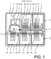
- the substrate 1 comprises a first metallization 3 which extends in two interconnected lines 5 extending along opposite edges 7 of the substrate 1.
- a second metallization 9 extends in an area 11 between the two lines 5 of the first metallization 3.
- the substrate 1 further comprises a third metallization 13 with a gate contact 15 and a gate area 17, which are interconnected by means of a bonding wire 19.
- the gate area 17 of the third metallization 13 extends in the area 11 between the two lines 5 of the first metallization 3, thereby dividing the second metallization 9 in two legs 20.
- multiple RC-IGBTs 21 are commonly mounted with their collectors on the first metallization 3.
- Emitter pads 23 of the RC-IGBTs 21 are bonded by means of bonding wires 19 to the second metallization 9, and gate pads 25 of the RC-IGBTs 21 are each bonded by means of a single bonding wire 19 to the third metallization 13.
- the substrates are typically mounted on a common base plate, which can be part of a housing of the power semiconductor module or which can be held within a housing of the power semiconductor module.
- a common base plate typically four or six substrates are combined, each provided with four to six power semiconductors comprising power transistors like insulated gate bipolar transistors (IGBT) or reverse conducting insulated gate bipolar transistors (RC-IGBT), power diodes, or other power semiconductors suitable for high power applications.
- a substrate can comprise four IGBTs and two power diodes.
- a power semiconductor module Important characteristics of a power semiconductor module are size, heat generation, cooling and maximum power. To facilitate the use of power semiconductor modules, it is desired to provide modules with a compact size, which require little space for mounting, and which are capable of use with high currents.
- EP 0 455 322 A1 discloses a substrate for mounting multiple power transistors thereon, with a first, second and third metallization. Furthermore, US 2002/0018353 A1 discloses a low-inductance circuit arrangement with two parallel metallizations with power transistors having the same orientation mounted thereon. Moreover, DE 195 49 011 A1 shows a semiconductor device with island-like gate metallization areas.
- the present invention provides substrate for mounting multiple power transistors thereon, comprising a first metallization, on which the power transistors are commonly mountable with their collector or emitter, and which extends in at least one line on the substrate, a second metallization, which extends in an area next to the at least one line of the first metallization, for connection to the remaining ones of the emitters or collectors of the power transistors, and a third metallization for connection to gate contact pads of the power transistors, whereby the third metallization comprises a gate contact and at least two gate metallization areas, which are interconnectable by way of bonding means, whereby the gate metallization areas are arranged in parallel to the at least one line and spaced apart in a longitudinal direction of the at least one line, and at least one gate metallization area is provided as a gate island surrounded on the substrate by the second metallization.
- the present invention also provides a power semiconductor module comprising at least one of the above substrates, whereby multiple power transistors are commonly mounted with their collectors or emitters on the first metallization of the at least one substrate, the remaining ones of the emitters or collectors of the power transistors are connected to the second metallization, gate pads of the power transistors are connected to the third metallization, and the gate contact and the at least two gate metallization areas are interconnected by way of bonding means.
- the basic idea of the invention is to provide the gate metallization with at least one gate island within the second metallization, so that an effective width of the second metallization is increased for the power semiconductors mountable on the substrate. Accordingly, current can flow from the power semiconductors over the entire width of the second metallization, so that the substrate can be used for high maximum currents.
- the gate metallization areas are preferably provided having a small extension within the second metallization, so that almost no extra space is required on the substrate, and the substrate can be kept small. Furthermore, space of the second metallization can be increased for connecting bonding means. An inductivity of the current power path, which includes the second metallization, is reduced due to the increased width of the second metallization.
- gate island With the gate island surrounded by the second metallization, an equilibrated coupling of the load current into the gate signals can be achieved.
- the bonding of gate pads of the power transistors can be easily realized by a suitable placement of the gate metallization areas, so that also the bonding of the second metallization to the power semiconductors can be improved.
- the second metallization is adapted for commonly mounting multiple power transistors with their collectors or emitters thereon, whereby the power transistors have the same orientation like the power transistors mounted on the first metallization
- the substrate comprises a fourth metallization, which extends in an area next to the second metallization, for connection to the remaining ones of the emitters or collectors of the power transistors mountable on the second metallization, and a fifth metallization for connection to gate contact pads of the power transistors mountable on the second metallization
- the fifth metallization comprises a gate contact and at least two gate metallization areas, which are interconnectable by way of bonding means, the gate metallization areas are arranged in parallel to the at least one line and spaced apart in a longitudinal direction of the at least one line, and at least one gate metallization area is provided as a gate island surrounded on the substrate by the fourth metallization.
- This arrangement provides a substrate for power semiconductors, which are mountable in series. Accordingly, the second metallization has a size for mounting the power transistors thereon.
- the same principles applicable to the first, second and third metallization equally apply to the second, fourth and fifth metallization, respectively.
- the resulting substrate enables a connection between the first and the fourth metallization with low resistance due to increased width of circuit paths thereon. More generally speaking, all circuit paths carrying high load currents can be provided with an increased cross section, which results in a reduced resistance.
- the design of the substrate allows the use of short bonding means for bonding the second and fourth metallization to the emitters or collectors of the power semiconductors, which increases life-time of the power semiconductor module and reduces its resistance. Coupling of the load current to gate voltages can be reduced, since the third and fifth metallization are surrounded by the second and fourth metallization, similar to a shielded coaxial cable.
- the power semiconductors can comprise the above-mentioned power transistors and optionally power diodes.
- the three metallizations are electrically separated from each other on the substrate.
- the substrate preferably has a connection area with contacts for at least the first and second metallization for connection of the substrate.
- the connection area provides an additional contact for the third metallization.
- the second and third metallization can be bonded to the power semiconductors by bonding means including bonding ribbons and bonding wires.
- the gate contact and the at least two gate metallization areas can be interconnected with the specified bonding means.
- the line of the first metallization is preferably a straight line extending in parallel to an edge of the substrate. Nevertheless, the line can also have a different form and position on the substrate.
- the first and second metallization can have an L-shape or a U-shape and extend in parallel to each other. Further preferred, the second metallization extends in parallel to the at least one line of the first metallization.
- the first metallization comprises two interconnected lines extending along opposite edges of the substrate, and the second metallization extends in an area between the two lines of the first metallization.
- the second metallization can be provided as a uniform area for connection of all semiconductors of the two lines. Accordingly, a further improvement can be achieved, since a current through power semiconductors of each line of the first metallization can flow over the entire width of the second metallization. Also bonding of the power semiconductors to the second metallization can be easily realized due to improved usage of the surface of the substrate.
- the first metallization is provided in a U-shape and extends through a connection area of the substrate.
- the connection area provides contacts for at least the first and second metallization for connection of the substrate.
- the connection area provides an additional contact for the third metallization.
- At least one gate metallization area is located centrally between the gate contact pads of power transistors of the two lines. This allows connecting the gate contact pads and the at least one gate metallization area using bonding means with a short length, which facilitates the bonding of the gate pads to the third metallization. Gate pads of power transistors belonging to the two lines can be connected with bonding means having the same length. Also bonding of the emitter or collector pads on top of the power transistors to the second metallization can be improved due to the improved bonding of the gate pads to the at least one gate island.
- the at least one gate metallization area is located centrally between gate pads of two power transistors.
- a respective power semiconductor module with such a substrate comprises multiple power transistors, which are commonly mounted with their collectors or emitters on the second metallization. The remaining ones of the emitters or collectors of the power transistors are connected to the fourth metallization, gate pads of the power transistors are connected to the fifth metallization, and the gate contact and the at least two gate metallization areas are interconnected by way of bonding means.
- This power semiconductor module comprises a series connection of two switches, so that it can be used for high voltages.
- the orientation of the power semiconductors on the second metallization is the same like the orientation of the power semiconductors on the first metallization, i.e. all power semiconductors are mounted either with their collector or emitter on the respective metallization.
- the same numbers of power transistors are mounted on the first and second metallization. Further preferred, the same type of power transistors are mounted on the first and second metallization.
- Substrates and power semiconductor modules can comprise further metallizations for providing a further series connection of power semiconductors within one module, whereby the same principles as described apply.
- the third metallization comprises a gate contact, which is interconnectable with the least two gate metallization areas by way of bonding means.
- the gate contact is used fo connection of the third metallization on the substrate.
- the gate contact is located in a connection area which provides contacts for the first and second metallization for connection of the substrate.
- the third metallization can be contacted on the substrate using a bonding means.
- the gate metallization areas of the third metallization can be directly contacted with a bonding wire from a respective metallization of an adjacent substrate.
- the third metallization comprises multiple gate islands.
- the multiple gate islands can be provided close to each of the gate pads of the power transistors, which facilitates the bonding between the gate pads of the power transistors and the gate metallization areas. Thereby, also the bonding between the power semiconductors and the second metallization is facilitated and improved.
- the length of the at least one gate island in a longitudinal direction of the at least one line is smaller than the extension of the power transistors in that direction.
- the full width of the second metallization is usable at each of the power semiconductors. Bottlenecks are avoided.
- the size of the at least one gate island in a direction perpendicular to the at least one line of the first metallization is between 0.5 mm and 3.0 mm, preferably between 1.0 mm and 2.0 mm.
- the second metallization experiences only a small reduction of size in the direction perpendicular to the at least one line of the first metallization, so that high currents can be carried by the second metallization.
- the at least two gate metallization areas are located centrally in the second metallization in respect to a direction perpendicular to the at least one line of the first metallization.
- the gate metallization areas are arranged in a central line within the second metallization, which provides the second metallization symmetrically on both sides of the gate metallization areas. Gate pads of power transistor belonging to both lines can be equally connected with bonding means having the same length.
- the at least two gate metallization areas are each separated from the second metallization by a gap with a width in the range from 0.5 mm to 2.0 mm.
- a reliable separation of the second and third metallization is provided, which enables small measures of the substrate and the power semiconductors module.
- one gate metallization area is provided as gate peninsula, which is surrounded on the substrate by the second metallization and an edge of the substrate. At the corner of the substrate, almost no current from power semiconductors located next to the corner has to be transported in the second metallization, so that the peninsula has only marginal influence on the current flow in the second metallization.
- the gate peninsula is provided at an edge of the substrate perpendicular to the opposite lines.
- a resistor is provided on and connected to the gate contact, and the gate metallization areas are bonded to the gate contact via the resistor.
- the gate resistor can be used to control the dynamic behavior of the power transistor. It can be easily mounted on the gate contact without requiring additional space on the substrate.
- the second metallization is provided in an L-shape and extends through a connection area of the substrate.
- the connection area provides contacts for at least the first and second metallization for connection of the substrate.
- the connection area provides an additional contact for the third metallization.
- the power transistors comprise multiple insulated gate bipolar transistors, and at least one power diode is mounted with one contact on the first metallization and connected with its contact pad for its other contact to the second metallization.
- This combination of power transistors and power diodes provides a suitable combination of features for power semiconductor modules. Further preferred, three IGBTs and two power diode are mounted on the first metallization.
- the power transistors comprise reverse conducting insulated gate bipolar transistors.
- the reverse conducting insulated gate bipolar transistors can be used without power diodes, since they have the functionality of power diodes integrated.
- a single kind of power transistors can be used for fitting to the substrate, so that the power semiconductor module can be easily manufactured.
- five RC-IGBTs are provided on each substrate. With the substrates comprising a fourth and a fifth metallization, three RC-IGBTs are mounted on each of the first and the second metallization.
- Fig. 2 shows a substrate 1 according to a first embodiment.
- the substrate 1 comprises a first metallization 3 which is provided in a U-shape. Accordingly, the first metallization 3 extends in two interconnected lines 5 extending along opposite edges 7 of the substrate 1 and along one connecting edge 8 connecting the opposite edges 7.
- the substrate 1 further comprises a second metallization 9, which is provided in an L-shape and extends in an area 11 between the two lines 5 of the first metallization 3.
- the substrate 1 also comprises a third metallization 13 with an individual gate contact 15 and three separate gate metallization areas 16, 18.
- the gate metallization areas 16, 18 are arranged between the two lines 5 and spaced apart in a direction parallel to the two lines 5.
- Two gate metallization areas 16 are provided as gate islands, which are entirely surrounded on the substrate 1 by the second metallization 9.
- the size of the gate islands 16 in a direction perpendicular to the lines 5 of the first metallization 3 is 2 mm in this embodiment.
- the third gate metallization area 18 is provided as gate peninsula, which is provided in a T-shape and surrounded on the substrate 1 by the second metallization 9 and a connecting edge 8 of the substrate 1.
- the gate metallization areas 16, 18 are each separated from the second metallization 9 by a gap 22 with a width of 1.0 mm in this embodiment.
- the substrate 1 comprises a connection area 24 for contacting the three metallizations 3, 9, 13. Accordingly, the first and second metallization 3, 9 extend through the connection area 24, and the gate contact 15 of the third metallization 13 is positioned in the connection area 24.
- RC-IGBT reverse conducting insulated gate bipolar transistors
- Emitter pads 23 of the RC-IGBTs 21 are bonded by means of bonding wires 19 to the second metallization 9
- gate pads 25 of the RC-IGBTs 21 are each bonded by means of a single bonding wire 19 to the gate metallization areas 16, 18 of the third metallization 13.
- the gate contact 15, the gate islands 16, and the gate peninsula 18 are interconnected by means of bonding wires 19.
- the gate islands 16 and the gate peninsula 18 are located centrally in the second metallization 9 in respect to a direction perpendicular to the two lines 5 of the first metallization 3.
- the gate islands 16 are further located centrally between gate pads 25 of RC-IGBTs 21 of the opposite lines 5.
- the length of the gate islands 16 in a longitudinal direction of the two lines 5 is smaller than the respective extension of the RC-IGBTs 21.
- a power semiconductor module which is not shown in the figures, comprises a base plate and multiple substrates 1 mounted thereon.
- the substrates 1 have an identical shape and design and are identically equipped with the power transistors 5 as described above.
- Fig. 3 shows a substrate 1 according to a second embodiment. Since the second embodiment is similar to the first embodiment, identical reference numerals are used for like components.
- the second embodiment only differs from the first embodiment in that different power semiconductors 30, 32 are mounted on the substrate 1.
- the power semiconductors 30, 32 comprise three insulated gate bipolar transistors 30 (IGBT) and two power diodes 32 in this embodiment.
- the IGBTs 30 according to the second embodiment are mounted and connected the same way like the RC-IGBTs 21 of the first embodiment.
- the power diodes 32 are mounted with one contact on the first metallization 3 and with a contact pad 34 for the other contact bonded to the second metallization 9. Accordingly, only gate pads 25 of the IGBTs 30 are bonded to the gate islands 16 and the gate peninsula 18.
- Fig. 4 shows a substrate 1 according to a third embodiment. Since the third embodiment is similar to the first embodiment, identical reference numerals are used for like components.
- the third embodiment only differs from the first embodiment in that a resistor 40 is provided on the gate contact 15 and electrically connected thereto by means of a bonding wire 19.
- the gate metallization areas 16, 18 are bonded to the gate contact 15 via the resistor 40.
- Fig. 5 shows a substrate 1 according to a fourth embodiment. Since the fourth embodiment is similar to the first embodiment, identical reference numerals are used for like components.
- the substrate 1 of the fourth embodiment comprises a first metallization 3 which is provided in a single line 5 extending along an edge 7 of the substrate 1.
- the substrate 1 further comprises a second metallization 9, which extends in an area 11 along the line 5 of the first metallization 3, and has a width big enough for mounting power semiconductors thereon.
- the substrate 1 also comprises a third metallization 13 with an individual gate contact 15 and three separate gate islands 16, which are entirely surrounded on the substrate 1 by the second metallization 9.
- the size of the gate islands 16 in a direction perpendicular to the line 5 of the first metallization 3 is 2 mm in this embodiment.
- the gate islands 16 are spaced apart in a direction parallel to the line 5.
- the gate islands 16 are each separated from the second metallization 9 by a gap 22 with a width of 1.0 mm in this embodiment.
- the substrate 1 comprises a fourth metallization 42, which has an L-shape and extends in an area 44 next to the second metallization 3.
- the substrate 1 further comprises a fifth metallization 46 with a gate contact 15, a gate interconnection area 48 and four gate metallization areas 16, which are provided as gate islands and surrounded on the substrate 1 by the fourth metallization 42.
- the gate islands16 are interconnected by way of bonding wires 19.
- the gate islands16 are arranged in parallel to the lines 5 of the first and second metallization 3, 9 and spaced apart in a longitudinal direction of these lines 5.
- a resistor 40 On the gate contact 15 of the third and fifth metallization 46 is provided a resistor 40, which is connected thereto by means of a bonding wire 19. The gate islands 16 are bonded to the respective gate contact 15 via the resistor 40.
- the substrate 1 comprises two connection areas 24 for contacting the metallizations 3, 9, 13, 42, 46.
- the connection areas 24 are positioned along the connecting edges 8 perpendicular to the lines 5 of the first and second metallizations 3, 9.
- RC-IGBT reverse conducting insulated gate bipolar transistors
- the gate islands 16, the gate contact and the interconnection area are interconnected by means of bonding wires 19.
- the gate islands 16 of the third metallization are located centrally in a space of the second metallization 9, which is not covered by the power transistors 21, in respect to a direction perpendicular to the lines 5 of the first and second metallization 3, 9.
- the gate islands 16 of the fifth metallization are located centrally in a space of the fourth metallization 42 in respect to a direction perpendicular to the lines 5 of the first and second metallization 3, 9.
- the RC-IGBTs 21 are arranged on the substrate providing two independent switches 50, 52, a first switch 50 between the first and second metallization 3, 9, and a second switch 52 between the second and fourth metallization 9, 42.
- the first switch 50 is controlled by via the third metallization 13 and the second switch 52 is controlled via the fifth metallization 46. Accordingly, a control signal provided via the third metallization 13 has to be defined in respect to the potential of the second metallization 9, and a control signal provided via the fifth metallization 46 has to be defined in respect to the potential of the fourth metallization 44.
- a power semiconductor module which is not shown in the figures, comprises a base plate and multiple substrates 1 mounted thereon.
- the substrates 1 have an identical shape and design and are identically equipped with the power transistors 5 as described above.
Landscapes
- Wire Bonding (AREA)
- Bipolar Transistors (AREA)
- Structure Of Printed Boards (AREA)
- Bipolar Integrated Circuits (AREA)
- Electrodes Of Semiconductors (AREA)
- Semiconductor Integrated Circuits (AREA)
Description
- The present invention relates to the area of substrates for mounting multiple power transistors thereon and of power semiconductor modules comprising such substrates and power transistors.
- Power semiconductor modules are used in high power applications to switch high voltages and currents and comprise multiple power semiconductors. Since each single semiconductor has a maximum voltage and current, the power semiconductors have to be combined in parallel and/or in series within the power semiconductor modules to enable the use in high power applications. To facilitate the manufacturing of such modules they commonly comprise multiple substrates, on which the power semiconductors are mounted. The substrates are provided with common contacts for emitter, collector and base, so that the substrates can easily be connected within the power semiconductor modules.
- A substrate according to the state of the art is shown in
Fig. 1 . Thesubstrate 1 comprises afirst metallization 3 which extends in twointerconnected lines 5 extending alongopposite edges 7 of thesubstrate 1. Asecond metallization 9 extends in anarea 11 between the twolines 5 of thefirst metallization 3. Thesubstrate 1 further comprises athird metallization 13 with agate contact 15 and a gate area 17, which are interconnected by means of abonding wire 19. The gate area 17 of thethird metallization 13 extends in thearea 11 between the twolines 5 of thefirst metallization 3, thereby dividing thesecond metallization 9 in twolegs 20. As can be seen inFig. 1 , multiple RC-IGBTs 21 are commonly mounted with their collectors on thefirst metallization 3.Emitter pads 23 of the RC-IGBTs 21 are bonded by means ofbonding wires 19 to thesecond metallization 9, andgate pads 25 of the RC-IGBTs 21 are each bonded by means of asingle bonding wire 19 to thethird metallization 13. - The substrates are typically mounted on a common base plate, which can be part of a housing of the power semiconductor module or which can be held within a housing of the power semiconductor module. In nowadays power semiconductor modules, typically four or six substrates are combined, each provided with four to six power semiconductors comprising power transistors like insulated gate bipolar transistors (IGBT) or reverse conducting insulated gate bipolar transistors (RC-IGBT), power diodes, or other power semiconductors suitable for high power applications. For example, a substrate can comprise four IGBTs and two power diodes.
- Important characteristics of a power semiconductor module are size, heat generation, cooling and maximum power. To facilitate the use of power semiconductor modules, it is desired to provide modules with a compact size, which require little space for mounting, and which are capable of use with high currents.
-
EP 0 455 322 A1 discloses a substrate for mounting multiple power transistors thereon, with a first, second and third metallization. Furthermore,US 2002/0018353 A1 discloses a low-inductance circuit arrangement with two parallel metallizations with power transistors having the same orientation mounted thereon. Moreover,DE 195 49 011 A1 shows a semiconductor device with island-like gate metallization areas. - It is an object of the present invention to provide a substrate and a power semiconductor module of the above-mentioned kind which are suitable for use in high power applications with high currents, which have a small size, and which are easily and economically mountable.
- This object is achieved by the independent claims. Advantageous embodiments are given in the dependent claims.
- In particular, the present invention provides substrate for mounting multiple power transistors thereon, comprising a first metallization, on which the power transistors are commonly mountable with their collector or emitter, and which extends in at least one line on the substrate, a second metallization, which extends in an area next to the at least one line of the first metallization, for connection to the remaining ones of the emitters or collectors of the power transistors, and a third metallization for connection to gate contact pads of the power transistors, whereby the third metallization comprises a gate contact and at least two gate metallization areas, which are interconnectable by way of bonding means, whereby the gate metallization areas are arranged in parallel to the at least one line and spaced apart in a longitudinal direction of the at least one line, and at least one gate metallization area is provided as a gate island surrounded on the substrate by the second metallization.
- The present invention also provides a power semiconductor module comprising at least one of the above substrates, whereby multiple power transistors are commonly mounted with their collectors or emitters on the first metallization of the at least one substrate, the remaining ones of the emitters or collectors of the power transistors are connected to the second metallization, gate pads of the power transistors are connected to the third metallization, and the gate contact and the at least two gate metallization areas are interconnected by way of bonding means.
- The basic idea of the invention is to provide the gate metallization with at least one gate island within the second metallization, so that an effective width of the second metallization is increased for the power semiconductors mountable on the substrate. Accordingly, current can flow from the power semiconductors over the entire width of the second metallization, so that the substrate can be used for high maximum currents. The gate metallization areas are preferably provided having a small extension within the second metallization, so that almost no extra space is required on the substrate, and the substrate can be kept small. Furthermore, space of the second metallization can be increased for connecting bonding means. An inductivity of the current power path, which includes the second metallization, is reduced due to the increased width of the second metallization. With the gate island surrounded by the second metallization, an equilibrated coupling of the load current into the gate signals can be achieved. The bonding of gate pads of the power transistors can be easily realized by a suitable placement of the gate metallization areas, so that also the bonding of the second metallization to the power semiconductors can be improved.
- According to a modified embodiment of the invention the second metallization is adapted for commonly mounting multiple power transistors with their collectors or emitters thereon, whereby the power transistors have the same orientation like the power transistors mounted on the first metallization, the substrate comprises a fourth metallization, which extends in an area next to the second metallization, for connection to the remaining ones of the emitters or collectors of the power transistors mountable on the second metallization, and a fifth metallization for connection to gate contact pads of the power transistors mountable on the second metallization, whereby the fifth metallization comprises a gate contact and at least two gate metallization areas, which are interconnectable by way of bonding means, the gate metallization areas are arranged in parallel to the at least one line and spaced apart in a longitudinal direction of the at least one line, and at least one gate metallization area is provided as a gate island surrounded on the substrate by the fourth metallization. This arrangement provides a substrate for power semiconductors, which are mountable in series. Accordingly, the second metallization has a size for mounting the power transistors thereon. The same principles applicable to the first, second and third metallization equally apply to the second, fourth and fifth metallization, respectively. The resulting substrate enables a connection between the first and the fourth metallization with low resistance due to increased width of circuit paths thereon. More generally speaking, all circuit paths carrying high load currents can be provided with an increased cross section, which results in a reduced resistance. The design of the substrate allows the use of short bonding means for bonding the second and fourth metallization to the emitters or collectors of the power semiconductors, which increases life-time of the power semiconductor module and reduces its resistance. Coupling of the load current to gate voltages can be reduced, since the third and fifth metallization are surrounded by the second and fourth metallization, similar to a shielded coaxial cable.
- The power semiconductors can comprise the above-mentioned power transistors and optionally power diodes. The three metallizations are electrically separated from each other on the substrate. The substrate preferably has a connection area with contacts for at least the first and second metallization for connection of the substrate. Optionally, the connection area provides an additional contact for the third metallization. The second and third metallization can be bonded to the power semiconductors by bonding means including bonding ribbons and bonding wires. The gate contact and the at least two gate metallization areas can be interconnected with the specified bonding means. The line of the first metallization is preferably a straight line extending in parallel to an edge of the substrate. Nevertheless, the line can also have a different form and position on the substrate. For example, the first and second metallization can have an L-shape or a U-shape and extend in parallel to each other. Further preferred, the second metallization extends in parallel to the at least one line of the first metallization.
- According to a modified embodiment it is conceivable, that the first metallization comprises two interconnected lines extending along opposite edges of the substrate, and the second metallization extends in an area between the two lines of the first metallization. The second metallization can be provided as a uniform area for connection of all semiconductors of the two lines. Accordingly, a further improvement can be achieved, since a current through power semiconductors of each line of the first metallization can flow over the entire width of the second metallization. Also bonding of the power semiconductors to the second metallization can be easily realized due to improved usage of the surface of the substrate.
- According to a further embodiment, the first metallization is provided in a U-shape and extends through a connection area of the substrate. The connection area provides contacts for at least the first and second metallization for connection of the substrate. Optionally, the connection area provides an additional contact for the third metallization. With the U-shape, the first metallization extends along three edges of the substrate and can easily be manufactured on the substrate.
- According to a modified embodiment, it is conceivable, that at least one gate metallization area is located centrally between the gate contact pads of power transistors of the two lines. This allows connecting the gate contact pads and the at least one gate metallization area using bonding means with a short length, which facilitates the bonding of the gate pads to the third metallization. Gate pads of power transistors belonging to the two lines can be connected with bonding means having the same length. Also bonding of the emitter or collector pads on top of the power transistors to the second metallization can be improved due to the improved bonding of the gate pads to the at least one gate island. Preferably, the at least one gate metallization area is located centrally between gate pads of two power transistors.
- A respective power semiconductor module with such a substrate comprises multiple power transistors, which are commonly mounted with their collectors or emitters on the second metallization. The remaining ones of the emitters or collectors of the power transistors are connected to the fourth metallization, gate pads of the power transistors are connected to the fifth metallization, and the gate contact and the at least two gate metallization areas are interconnected by way of bonding means. This power semiconductor module comprises a series connection of two switches, so that it can be used for high voltages. The orientation of the power semiconductors on the second metallization is the same like the orientation of the power semiconductors on the first metallization, i.e. all power semiconductors are mounted either with their collector or emitter on the respective metallization. Preferably, the same numbers of power transistors are mounted on the first and second metallization. Further preferred, the same type of power transistors are mounted on the first and second metallization. Substrates and power semiconductor modules can comprise further metallizations for providing a further series connection of power semiconductors within one module, whereby the same principles as described apply.
- According to a modified embodiment of the invention the third metallization comprises a gate contact, which is interconnectable with the least two gate metallization areas by way of bonding means. The gate contact is used fo connection of the third metallization on the substrate. Further preferred, the gate contact is located in a connection area which provides contacts for the first and second metallization for connection of the substrate. Alternatively, the third metallization can be contacted on the substrate using a bonding means. For example, when mounted in a semiconductor module, the gate metallization areas of the third metallization can be directly contacted with a bonding wire from a respective metallization of an adjacent substrate.
- According to a modified embodiment of the invention the third metallization comprises multiple gate islands. The multiple gate islands can be provided close to each of the gate pads of the power transistors, which facilitates the bonding between the gate pads of the power transistors and the gate metallization areas. Thereby, also the bonding between the power semiconductors and the second metallization is facilitated and improved.
- According to a modified embodiment of the invention the length of the at least one gate island in a longitudinal direction of the at least one line is smaller than the extension of the power transistors in that direction. Hence, the full width of the second metallization is usable at each of the power semiconductors. Bottlenecks are avoided.
- According to a modified embodiment of the invention the size of the at least one gate island in a direction perpendicular to the at least one line of the first metallization is between 0.5 mm and 3.0 mm, preferably between 1.0 mm and 2.0 mm. With this width of the at least one gate island, the second metallization experiences only a small reduction of size in the direction perpendicular to the at least one line of the first metallization, so that high currents can be carried by the second metallization.
- According to a modified embodiment of the invention the at least two gate metallization areas are located centrally in the second metallization in respect to a direction perpendicular to the at least one line of the first metallization. In other words, the gate metallization areas are arranged in a central line within the second metallization, which provides the second metallization symmetrically on both sides of the gate metallization areas. Gate pads of power transistor belonging to both lines can be equally connected with bonding means having the same length.
- According to a modified embodiment of the invention the at least two gate metallization areas are each separated from the second metallization by a gap with a width in the range from 0.5 mm to 2.0 mm. A reliable separation of the second and third metallization is provided, which enables small measures of the substrate and the power semiconductors module.
- According to a modified embodiment of the invention one gate metallization area is provided as gate peninsula, which is surrounded on the substrate by the second metallization and an edge of the substrate. At the corner of the substrate, almost no current from power semiconductors located next to the corner has to be transported in the second metallization, so that the peninsula has only marginal influence on the current flow in the second metallization. Preferably, the gate peninsula is provided at an edge of the substrate perpendicular to the opposite lines.
- According to a modified embodiment of the invention a resistor is provided on and connected to the gate contact, and the gate metallization areas are bonded to the gate contact via the resistor. The gate resistor can be used to control the dynamic behavior of the power transistor. It can be easily mounted on the gate contact without requiring additional space on the substrate.
- According to a modified embodiment of the invention the second metallization is provided in an L-shape and extends through a connection area of the substrate. The connection area provides contacts for at least the first and second metallization for connection of the substrate. Optionally, the connection area provides an additional contact for the third metallization. With the L-shape, the second metallization extends between along the at least one line of the first metallization and can be easily contacted in the connection area.
- According to a modified embodiment of the invention the power transistors comprise multiple insulated gate bipolar transistors, and at least one power diode is mounted with one contact on the first metallization and connected with its contact pad for its other contact to the second metallization. This combination of power transistors and power diodes provides a suitable combination of features for power semiconductor modules. Further preferred, three IGBTs and two power diode are mounted on the first metallization.
- According to a modified embodiment of the invention the power transistors comprise reverse conducting insulated gate bipolar transistors. The reverse conducting insulated gate bipolar transistors (RC-IGBT) can be used without power diodes, since they have the functionality of power diodes integrated. A single kind of power transistors can be used for fitting to the substrate, so that the power semiconductor module can be easily manufactured. Further preferred, five RC-IGBTs are provided on each substrate. With the substrates comprising a fourth and a fifth metallization, three RC-IGBTs are mounted on each of the first and the second metallization.
- These and other aspects of the invention will be apparent from and elucidated with reference to the embodiments described hereinafter.
- In the drawings:
-
Fig. 1 shows a schematical drawing of a substrate with multiple power transistors mounted thereon according to the state of the art, -
Fig. 2 shows a schematical drawing of a substrate according to a first embodiment with multiple power transistors mounted thereon, -
Fig. 3 shows a schematical drawing of a substrate according to a second embodiment with multiple power transistors and power diodes mounted thereon, -
Fig. 4 shows a schematical drawing of a substrate according to a third embodiment with an additional gate resistor compared to the embodiment ofFig. 2 , and -
Fig. 5 shows a schematical drawing of a substrate according to a fourth embodiment with multiple power transistors mounted thereon in two groups forming two switches arranged in series. -
Fig. 2 shows asubstrate 1 according to a first embodiment. Thesubstrate 1 comprises afirst metallization 3 which is provided in a U-shape. Accordingly, thefirst metallization 3 extends in twointerconnected lines 5 extending alongopposite edges 7 of thesubstrate 1 and along one connectingedge 8 connecting the opposite edges 7. - The
substrate 1 further comprises asecond metallization 9, which is provided in an L-shape and extends in anarea 11 between the twolines 5 of thefirst metallization 3. - The
substrate 1 also comprises athird metallization 13 with anindividual gate contact 15 and three separategate metallization areas gate metallization areas lines 5 and spaced apart in a direction parallel to the twolines 5. Twogate metallization areas 16 are provided as gate islands, which are entirely surrounded on thesubstrate 1 by thesecond metallization 9. The size of thegate islands 16 in a direction perpendicular to thelines 5 of thefirst metallization 3 is 2 mm in this embodiment. The thirdgate metallization area 18 is provided as gate peninsula, which is provided in a T-shape and surrounded on thesubstrate 1 by thesecond metallization 9 and a connectingedge 8 of thesubstrate 1. Thegate metallization areas second metallization 9 by agap 22 with a width of 1.0 mm in this embodiment. - The
substrate 1 comprises aconnection area 24 for contacting the threemetallizations second metallization connection area 24, and thegate contact 15 of thethird metallization 13 is positioned in theconnection area 24. - As can be seen in
Fig. 2 , fivepower transistors 21, which are identical reverse conducting insulated gate bipolar transistors (RC-IGBT) in this embodiment, are commonly mounted with their collectors on thefirst metallization 3.Emitter pads 23 of the RC-IGBTs 21 are bonded by means ofbonding wires 19 to thesecond metallization 9, andgate pads 25 of the RC-IGBTs 21 are each bonded by means of asingle bonding wire 19 to thegate metallization areas third metallization 13. On the mountedsubstrate 1, thegate contact 15, thegate islands 16, and thegate peninsula 18 are interconnected by means ofbonding wires 19. - According to
Fig. 2 , thegate islands 16 and thegate peninsula 18 are located centrally in thesecond metallization 9 in respect to a direction perpendicular to the twolines 5 of thefirst metallization 3. Thegate islands 16 are further located centrally betweengate pads 25 of RC-IGBTs 21 of theopposite lines 5. The length of thegate islands 16 in a longitudinal direction of the twolines 5 is smaller than the respective extension of the RC-IGBTs 21. - A power semiconductor module according to this embodiment, which is not shown in the figures, comprises a base plate and
multiple substrates 1 mounted thereon. Thesubstrates 1 have an identical shape and design and are identically equipped with thepower transistors 5 as described above. -
Fig. 3 shows asubstrate 1 according to a second embodiment. Since the second embodiment is similar to the first embodiment, identical reference numerals are used for like components. - The second embodiment only differs from the first embodiment in that
different power semiconductors substrate 1. Thepower semiconductors power diodes 32 in this embodiment. TheIGBTs 30 according to the second embodiment are mounted and connected the same way like the RC-IGBTs 21 of the first embodiment. Thepower diodes 32 are mounted with one contact on thefirst metallization 3 and with acontact pad 34 for the other contact bonded to thesecond metallization 9. Accordingly, onlygate pads 25 of theIGBTs 30 are bonded to thegate islands 16 and thegate peninsula 18. -
Fig. 4 shows asubstrate 1 according to a third embodiment. Since the third embodiment is similar to the first embodiment, identical reference numerals are used for like components. - The third embodiment only differs from the first embodiment in that a
resistor 40 is provided on thegate contact 15 and electrically connected thereto by means of abonding wire 19. Thegate metallization areas gate contact 15 via theresistor 40. -
Fig. 5 shows asubstrate 1 according to a fourth embodiment. Since the fourth embodiment is similar to the first embodiment, identical reference numerals are used for like components. - The
substrate 1 of the fourth embodiment comprises afirst metallization 3 which is provided in asingle line 5 extending along anedge 7 of thesubstrate 1. - The
substrate 1 further comprises asecond metallization 9, which extends in anarea 11 along theline 5 of thefirst metallization 3, and has a width big enough for mounting power semiconductors thereon. - The
substrate 1 also comprises athird metallization 13 with anindividual gate contact 15 and threeseparate gate islands 16, which are entirely surrounded on thesubstrate 1 by thesecond metallization 9. The size of thegate islands 16 in a direction perpendicular to theline 5 of thefirst metallization 3 is 2 mm in this embodiment. Thegate islands 16 are spaced apart in a direction parallel to the line 5.Thegate islands 16 are each separated from thesecond metallization 9 by agap 22 with a width of 1.0 mm in this embodiment. - The
substrate 1 comprises afourth metallization 42, which has an L-shape and extends in anarea 44 next to thesecond metallization 3. Thesubstrate 1 further comprises afifth metallization 46 with agate contact 15, agate interconnection area 48 and fourgate metallization areas 16, which are provided as gate islands and surrounded on thesubstrate 1 by thefourth metallization 42. The gate islands16 are interconnected by way ofbonding wires 19. The gate islands16 are arranged in parallel to thelines 5 of the first andsecond metallization lines 5. - On the
gate contact 15 of the third andfifth metallization 46 is provided aresistor 40, which is connected thereto by means of abonding wire 19. Thegate islands 16 are bonded to therespective gate contact 15 via theresistor 40. - The
substrate 1 comprises twoconnection areas 24 for contacting themetallizations connection areas 24 are positioned along the connectingedges 8 perpendicular to thelines 5 of the first andsecond metallizations - As can be further seen in
Fig. 5 , sixpower transistors 21, which are identical reverse conducting insulated gate bipolar transistors (RC-IGBT) in this embodiment, are commonly mounted with their collectors on the first andsecond metallization IGBTs 21 are mounted on thefirst metallization 3 and three RC-IGBTs 21 are mounted on thesecond metallization 9.Emitter pads 23 of the RC-IGBTs 21 are bonded by means ofbonding wires 19 to the second andfourth metallization gate pads 25 of the RC-IGBTs 21 are each bonded by means of asingle bonding wire 19 togate islands 16 of the third andfifth metallization substrate 1, thegate islands 16, the gate contact and the interconnection area are interconnected by means ofbonding wires 19. As can be seen inFig. 5 , thegate islands 16 of the third metallization are located centrally in a space of thesecond metallization 9, which is not covered by thepower transistors 21, in respect to a direction perpendicular to thelines 5 of the first andsecond metallization gate islands 16 of the fifth metallization are located centrally in a space of thefourth metallization 42 in respect to a direction perpendicular to thelines 5 of the first andsecond metallization - The RC-
IGBTs 21 are arranged on the substrate providing twoindependent switches first switch 50 between the first andsecond metallization second switch 52 between the second andfourth metallization first switch 50 is controlled by via thethird metallization 13 and thesecond switch 52 is controlled via thefifth metallization 46. Accordingly, a control signal provided via thethird metallization 13 has to be defined in respect to the potential of thesecond metallization 9, and a control signal provided via thefifth metallization 46 has to be defined in respect to the potential of thefourth metallization 44. - A power semiconductor module according to this embodiment, which is not shown in the figures, comprises a base plate and
multiple substrates 1 mounted thereon. Thesubstrates 1 have an identical shape and design and are identically equipped with thepower transistors 5 as described above. -
- 1
- substrate
- 3
- first metallization
- 5
- line
- 7
- edge
- 8
- connecting edge
- 9
- second metallization
- 11
- area between the lines
- 13
- third metallization
- 15
- gate contact
- 16
- gate metallization area, gate island
- 17
- gate area
- 18
- gate metallization area, gate peninsula
- 19
- bonding wire
- 20
- leg
- 21
- power transistor, RC-IGBT
- 22
- gap
- 23
- emitter pad
- 24
- connection area
- 25
- gate pad
- 30
- power transistor, IGBT
- 32
- power diode
- 34
- contact pad
- 40
- resistor
- 42
- fourth metallization
- 44
- area
- 46
- fifth metallization
- 48
- interconnection area
- 50
- first switch
- 52
- second switch
Claims (11)
- Substrate (1) comprising multiple power transistors (21, 30) mounted thereon, comprising
a first metallization (3), on which the power transistors (21, 30) are mounted with their collector or emitter, and which extends in at least one line (5) on the substrate (1),
a second metallization (9), which extends in an area (11) next to the at least one line (5) of the first metallization (3), connected to the remaining ones of the emitters or collectors of the power transistors (21, 30), and
a third metallization (13) connected to gate contact pads (25) of the power transistors (21,30),
whereby the third metallization (13) comprises at least two gate metallization areas (16, 18), which are connected by way of bonding means (19), whereby
the gate metallization areas (16, 18) are arranged in parallel to the at least one line (5) and spaced apart in a longitudinal direction of the at least one line (5),
at least one gate metallization area is provided as a gate island (16) surrounded on the substrate (1) by the second metallization (9),
the second metallization (9) has multiple power transistors (21, 30) with their collectors or emitters mounted thereon, whereby the power transistors (21, 30) have the same orientation like the power transistors (21, 30) mounted on the first metallization (3), the substrate (1) comprises a fourth metallization (42), which extends in an area (44) next to the second metallization (9), connected to the remaining ones of the emitters or collectors of the power transistors (21, 30) mounted on the second metallization (9), and
a fifth metallization (46) connected to gate contact pads (25) of the power transistors (21, 30) mounted on the second metallization (9), whereby
the fifth metallization (46) comprises at least two gate metallization areas (16, 18), which are interconnected by way of bonding means (19), the gate metallization areas (16, 18) are arranged in parallel to the at least one line (5) and spaced apart in a longitudinal direction of the at least one line (5), and
at least one gate metallization area is provided as a gate island (16) surrounded on the substrate (1) by the fourth metallization (42). - Substrate (1) according to any preceding claim, characterized in that the third metallization (13) comprises a gate contact (15), which is interconnectable with the at least two gate metallization areas (16, 18) by way of bonding means (19).
- Substrate (1) according to any preceding claim, characterized in that the length of the at least one gate island (16) in a longitudinal direction of the at least one line (5) is smaller than the extension of the power transistors (21, 30) in that direction.
- Substrate (1) according to any preceding claim, characterized in that the size of the at least one gate island (16) in a direction perpendicular to the at least one line (5) of the first metallization (3) is between 0.5 mm and 3.0 mm, preferably between 1.0 mm and 2.0 mm.
- Substrate (1) according to any preceding claim, characterized in that the at least two gate metallization areas (16, 18) are located centrally in the second metallization (9) in respect to a direction perpendicular to the at least one line (5) of the first metallization (3).
- Substrate (1) according to any preceding claim, characterized in that the at least two gate metallization areas (16, 18) are each separated from the second metallization (9) by a gap (22) with a width in the range from 0.5 mm to 2.0 mm.
- Substrate (1) according to any preceding claim, characterized in that one gate metallization area is provided as gate contact (15), which is surrounded on the substrate (1) by the second metallization (9) and an edge (8) of the substrate (1).
- Substrate (1) according to any preceding claim, characterized in that the fourth metallization (42) is provided in an L-shape and extends through a connection area (24) of the substrate (1).
- Substrate (1) according to any preceding claim, characterized in that a resistor (40) is provided on and connected to the gate contact (15), and the gate metallization areas (16, 18) are bonded to the gate contact (15) via the resistor (40).
- Power semiconductor module comprising at least one substrate (1) according to any preceding claim, whereby
multiple power transistors (21, 30) are commonly mounted with their collectors or emitters on the first metallization (3) of the at least one substrate (1),
the remaining ones of the emitters or collectors of the power transistors (21, 30) are connected to the second metallization (9),
gate pads (25) of the power transistors (21, 30) are connected to the third metallization (13), and
the gate contact (15) and the at least two gate metallization areas (16, 18) are interconnected by way of bonding means (19). - Power semiconductor module according to preceding claim 10, whereby multiple power transistors (21, 30) are commonly mounted with their collectors or emitters on the second metallization (9),
the remaining ones of the emitters or collectors of the power transistors (21, 30) are connected to the fourth metallization (),
gate pads (25) of the power transistors (21, 30) are connected to the fifth metallization (13), and
the gate contact (15) and the at least two gate metallization areas (16, 18) are interconnected by way of bonding means (19).
Priority Applications (1)
| Application Number | Priority Date | Filing Date | Title |
|---|---|---|---|
| EP13729005.2A EP2862202B1 (en) | 2012-06-19 | 2013-06-06 | Substrate for mounting multiple power transistors thereon and power semiconductor module |
Applications Claiming Priority (3)
| Application Number | Priority Date | Filing Date | Title |
|---|---|---|---|
| EP12172514 | 2012-06-19 | ||
| PCT/EP2013/061735 WO2013189756A1 (en) | 2012-06-19 | 2013-06-06 | Substrate for mounting multiple power transistors thereon and power semiconductor module |
| EP13729005.2A EP2862202B1 (en) | 2012-06-19 | 2013-06-06 | Substrate for mounting multiple power transistors thereon and power semiconductor module |
Publications (2)
| Publication Number | Publication Date |
|---|---|
| EP2862202A1 EP2862202A1 (en) | 2015-04-22 |
| EP2862202B1 true EP2862202B1 (en) | 2016-04-27 |
Family
ID=48626435
Family Applications (1)
| Application Number | Title | Priority Date | Filing Date |
|---|---|---|---|
| EP13729005.2A Not-in-force EP2862202B1 (en) | 2012-06-19 | 2013-06-06 | Substrate for mounting multiple power transistors thereon and power semiconductor module |
Country Status (5)
| Country | Link |
|---|---|
| US (1) | US9431376B2 (en) |
| EP (1) | EP2862202B1 (en) |
| JP (1) | JP5876970B2 (en) |
| CN (1) | CN104380463B (en) |
| WO (1) | WO2013189756A1 (en) |
Families Citing this family (11)
| Publication number | Priority date | Publication date | Assignee | Title |
|---|---|---|---|---|
| DE102014111931B4 (en) * | 2014-08-20 | 2021-07-08 | Infineon Technologies Ag | Low-inductance circuit arrangement with load current busbar |
| JP6344197B2 (en) * | 2014-10-30 | 2018-06-20 | 富士電機株式会社 | Semiconductor device |
| CN106415834B (en) * | 2014-11-28 | 2019-09-13 | 富士电机株式会社 | semiconductor device |
| WO2017071976A1 (en) * | 2015-10-29 | 2017-05-04 | Abb Schweiz Ag | Semiconductor module |
| JP2017162866A (en) * | 2016-03-07 | 2017-09-14 | 株式会社東芝 | Semiconductor device |
| JP6598739B2 (en) * | 2016-07-14 | 2019-10-30 | 三菱電機株式会社 | Semiconductor module |
| CN107958905B (en) * | 2017-12-11 | 2024-06-21 | 柳州臻驱电控科技有限公司 | Power semiconductor module substrate |
| US10418307B2 (en) * | 2017-12-22 | 2019-09-17 | Deere & Company | Electronic assembly with a direct bonded copper substrate |
| CN111987089A (en) * | 2020-08-19 | 2020-11-24 | 株洲中车时代半导体有限公司 | Reverse conducting IGBT power integrated module |
| CN113053850A (en) * | 2021-03-16 | 2021-06-29 | 苏州悉智科技有限公司 | Power Module Package Structure |
| DE102022113195B4 (en) * | 2022-05-25 | 2025-11-06 | Audi Aktiengesellschaft | Power electronics arrangement with parallel-connected semiconductor switches, power electronics device, motor vehicle and method for manufacturing a power electronics arrangement |
Family Cites Families (19)
| Publication number | Priority date | Publication date | Assignee | Title |
|---|---|---|---|---|
| JPH088269B2 (en) * | 1986-10-22 | 1996-01-29 | シーメンス、アクチエンゲゼルシヤフト | Semiconductor device |
| JPH03263363A (en) | 1990-02-23 | 1991-11-22 | Fuji Electric Co Ltd | Semiconductor device |
| JP2725952B2 (en) * | 1992-06-30 | 1998-03-11 | 三菱電機株式会社 | Semiconductor power module |
| JP2973799B2 (en) * | 1993-04-23 | 1999-11-08 | 富士電機株式会社 | Power transistor module |
| JP3476612B2 (en) * | 1995-12-21 | 2003-12-10 | 三菱電機株式会社 | Semiconductor device |
| DE19549011C2 (en) * | 1995-12-28 | 1998-12-03 | Eupec Gmbh & Co Kg | Power semiconductor module with parallel IGBT chips and additional connection of the emitter contacts |
| JP4088394B2 (en) * | 1999-09-29 | 2008-05-21 | 株式会社日立製作所 | Insulated circuit board and semiconductor device using the same |
| DE10037533C1 (en) * | 2000-08-01 | 2002-01-31 | Semikron Elektronik Gmbh | Low-inductance circuit arrangement |
| ATE339013T1 (en) * | 2002-01-29 | 2006-09-15 | Advanced Power Technology | SPLIT GATE POWER MODULE AND METHOD FOR SUPPRESSING VIBRATIONS THEREIN |
| EP1594164B1 (en) * | 2003-02-14 | 2012-05-09 | Hitachi, Ltd. | Integrated circuit for driving semiconductor device |
| DE10316136A1 (en) * | 2003-04-09 | 2004-11-18 | Ixys Semiconductor Gmbh | Encapsulated power semiconductor arrangement |
| DE102006038479B4 (en) * | 2006-08-17 | 2011-01-27 | Infineon Technologies Ag | Power semiconductor module with two multiple power semiconductor devices |
| JP4988784B2 (en) * | 2009-03-30 | 2012-08-01 | 株式会社日立製作所 | Power semiconductor device |
| CN102576705B (en) * | 2009-09-28 | 2015-10-21 | Abb技术有限公司 | Circuit arrangement and manufacture method thereof |
| JP5312386B2 (en) * | 2010-03-23 | 2013-10-09 | 日立オートモティブシステムズ株式会社 | Power converter |
| JP5789264B2 (en) * | 2010-09-24 | 2015-10-07 | セミコンダクター・コンポーネンツ・インダストリーズ・リミテッド・ライアビリティ・カンパニー | Circuit equipment |
| US8487407B2 (en) * | 2011-10-13 | 2013-07-16 | Infineon Technologies Ag | Low impedance gate control method and apparatus |
| US9209176B2 (en) * | 2011-12-07 | 2015-12-08 | Transphorm Inc. | Semiconductor modules and methods of forming the same |
| EP2660863B1 (en) * | 2012-05-02 | 2019-07-10 | ABB Schweiz AG | Power semiconductor module |
-
2013
- 2013-06-06 EP EP13729005.2A patent/EP2862202B1/en not_active Not-in-force
- 2013-06-06 WO PCT/EP2013/061735 patent/WO2013189756A1/en not_active Ceased
- 2013-06-06 JP JP2015516563A patent/JP5876970B2/en not_active Expired - Fee Related
- 2013-06-06 CN CN201380032411.2A patent/CN104380463B/en not_active Expired - Fee Related
-
2014
- 2014-11-12 US US14/539,422 patent/US9431376B2/en not_active Expired - Fee Related
Also Published As
| Publication number | Publication date |
|---|---|
| CN104380463B (en) | 2017-05-10 |
| US9431376B2 (en) | 2016-08-30 |
| EP2862202A1 (en) | 2015-04-22 |
| JP5876970B2 (en) | 2016-03-02 |
| JP2015519760A (en) | 2015-07-09 |
| US20150069463A1 (en) | 2015-03-12 |
| CN104380463A (en) | 2015-02-25 |
| WO2013189756A1 (en) | 2013-12-27 |
Similar Documents
| Publication | Publication Date | Title |
|---|---|---|
| US9431376B2 (en) | Substrate for mounting multiple power transistors thereon and power semiconductor module | |
| US11171122B2 (en) | Semiconductor device | |
| JP7153649B2 (en) | Power semiconductor modules with low gate path inductance | |
| US9659912B2 (en) | Low-inductance circuit arrangement comprising load current collecting conductor track | |
| US9106124B2 (en) | Low-inductance power semiconductor assembly | |
| US10903158B2 (en) | Semiconductor arrangement having a circuit board with a patterned metallization layer | |
| JP7210446B2 (en) | power semiconductor module | |
| JP4955077B2 (en) | Semiconductor device | |
| CN108933116B (en) | Semiconductor package with lead frame | |
| US10361136B2 (en) | Semiconductor device and semiconductor module provided with same | |
| JP6623283B2 (en) | Power semiconductor module | |
| US10276552B2 (en) | Semiconductor module | |
| JP4484400B2 (en) | Semiconductor device | |
| US7821128B2 (en) | Power semiconductor device having lines within a housing | |
| CN112447612A (en) | Multi-chip package | |
| KR20120012407A (en) | Power Semiconductor Modules and Submodules | |
| US11158569B2 (en) | Semiconductor component and semiconductor package | |
| US11973065B2 (en) | Semiconductor arrangements | |
| JP7746241B2 (en) | Semiconductor Module |
Legal Events
| Date | Code | Title | Description |
|---|---|---|---|
| PUAI | Public reference made under article 153(3) epc to a published international application that has entered the european phase |
Free format text: ORIGINAL CODE: 0009012 |
|
| 17P | Request for examination filed |
Effective date: 20141021 |
|
| AK | Designated contracting states |
Kind code of ref document: A1 Designated state(s): AL AT BE BG CH CY CZ DE DK EE ES FI FR GB GR HR HU IE IS IT LI LT LU LV MC MK MT NL NO PL PT RO RS SE SI SK SM TR |
|
| AX | Request for extension of the european patent |
Extension state: BA ME |
|
| DAX | Request for extension of the european patent (deleted) | ||
| GRAP | Despatch of communication of intention to grant a patent |
Free format text: ORIGINAL CODE: EPIDOSNIGR1 |
|
| INTG | Intention to grant announced |
Effective date: 20151221 |
|
| GRAS | Grant fee paid |
Free format text: ORIGINAL CODE: EPIDOSNIGR3 |
|
| GRAA | (expected) grant |
Free format text: ORIGINAL CODE: 0009210 |
|
| AK | Designated contracting states |
Kind code of ref document: B1 Designated state(s): AL AT BE BG CH CY CZ DE DK EE ES FI FR GB GR HR HU IE IS IT LI LT LU LV MC MK MT NL NO PL PT RO RS SE SI SK SM TR |
|
| REG | Reference to a national code |
Ref country code: GB Ref legal event code: FG4D |
|
| REG | Reference to a national code |
Ref country code: CH Ref legal event code: EP |
|
| REG | Reference to a national code |
Ref country code: AT Ref legal event code: REF Ref document number: 795640 Country of ref document: AT Kind code of ref document: T Effective date: 20160515 |
|
| REG | Reference to a national code |
Ref country code: IE Ref legal event code: FG4D |
|
| REG | Reference to a national code |
Ref country code: DE Ref legal event code: R096 Ref document number: 602013007086 Country of ref document: DE |
|
| PGFP | Annual fee paid to national office [announced via postgrant information from national office to epo] |
Ref country code: DE Payment date: 20160621 Year of fee payment: 4 |
|
| REG | Reference to a national code |
Ref country code: LT Ref legal event code: MG4D |
|
| REG | Reference to a national code |
Ref country code: NL Ref legal event code: MP Effective date: 20160427 |
|
| REG | Reference to a national code |
Ref country code: AT Ref legal event code: MK05 Ref document number: 795640 Country of ref document: AT Kind code of ref document: T Effective date: 20160427 |
|
| PG25 | Lapsed in a contracting state [announced via postgrant information from national office to epo] |
Ref country code: NL Free format text: LAPSE BECAUSE OF FAILURE TO SUBMIT A TRANSLATION OF THE DESCRIPTION OR TO PAY THE FEE WITHIN THE PRESCRIBED TIME-LIMIT Effective date: 20160427 |
|
| PG25 | Lapsed in a contracting state [announced via postgrant information from national office to epo] |
Ref country code: NO Free format text: LAPSE BECAUSE OF FAILURE TO SUBMIT A TRANSLATION OF THE DESCRIPTION OR TO PAY THE FEE WITHIN THE PRESCRIBED TIME-LIMIT Effective date: 20160727 Ref country code: LT Free format text: LAPSE BECAUSE OF FAILURE TO SUBMIT A TRANSLATION OF THE DESCRIPTION OR TO PAY THE FEE WITHIN THE PRESCRIBED TIME-LIMIT Effective date: 20160427 Ref country code: PL Free format text: LAPSE BECAUSE OF FAILURE TO SUBMIT A TRANSLATION OF THE DESCRIPTION OR TO PAY THE FEE WITHIN THE PRESCRIBED TIME-LIMIT Effective date: 20160427 Ref country code: FI Free format text: LAPSE BECAUSE OF FAILURE TO SUBMIT A TRANSLATION OF THE DESCRIPTION OR TO PAY THE FEE WITHIN THE PRESCRIBED TIME-LIMIT Effective date: 20160427 |
|
| PG25 | Lapsed in a contracting state [announced via postgrant information from national office to epo] |
Ref country code: GR Free format text: LAPSE BECAUSE OF FAILURE TO SUBMIT A TRANSLATION OF THE DESCRIPTION OR TO PAY THE FEE WITHIN THE PRESCRIBED TIME-LIMIT Effective date: 20160728 Ref country code: HR Free format text: LAPSE BECAUSE OF FAILURE TO SUBMIT A TRANSLATION OF THE DESCRIPTION OR TO PAY THE FEE WITHIN THE PRESCRIBED TIME-LIMIT Effective date: 20160427 Ref country code: RS Free format text: LAPSE BECAUSE OF FAILURE TO SUBMIT A TRANSLATION OF THE DESCRIPTION OR TO PAY THE FEE WITHIN THE PRESCRIBED TIME-LIMIT Effective date: 20160427 Ref country code: AT Free format text: LAPSE BECAUSE OF FAILURE TO SUBMIT A TRANSLATION OF THE DESCRIPTION OR TO PAY THE FEE WITHIN THE PRESCRIBED TIME-LIMIT Effective date: 20160427 Ref country code: ES Free format text: LAPSE BECAUSE OF FAILURE TO SUBMIT A TRANSLATION OF THE DESCRIPTION OR TO PAY THE FEE WITHIN THE PRESCRIBED TIME-LIMIT Effective date: 20160427 Ref country code: SE Free format text: LAPSE BECAUSE OF FAILURE TO SUBMIT A TRANSLATION OF THE DESCRIPTION OR TO PAY THE FEE WITHIN THE PRESCRIBED TIME-LIMIT Effective date: 20160427 Ref country code: PT Free format text: LAPSE BECAUSE OF FAILURE TO SUBMIT A TRANSLATION OF THE DESCRIPTION OR TO PAY THE FEE WITHIN THE PRESCRIBED TIME-LIMIT Effective date: 20160829 Ref country code: LV Free format text: LAPSE BECAUSE OF FAILURE TO SUBMIT A TRANSLATION OF THE DESCRIPTION OR TO PAY THE FEE WITHIN THE PRESCRIBED TIME-LIMIT Effective date: 20160427 |
|
| PG25 | Lapsed in a contracting state [announced via postgrant information from national office to epo] |
Ref country code: BE Free format text: LAPSE BECAUSE OF FAILURE TO SUBMIT A TRANSLATION OF THE DESCRIPTION OR TO PAY THE FEE WITHIN THE PRESCRIBED TIME-LIMIT Effective date: 20160427 Ref country code: IT Free format text: LAPSE BECAUSE OF FAILURE TO SUBMIT A TRANSLATION OF THE DESCRIPTION OR TO PAY THE FEE WITHIN THE PRESCRIBED TIME-LIMIT Effective date: 20160427 |
|
| REG | Reference to a national code |
Ref country code: DE Ref legal event code: R097 Ref document number: 602013007086 Country of ref document: DE |
|
| PG25 | Lapsed in a contracting state [announced via postgrant information from national office to epo] |
Ref country code: DK Free format text: LAPSE BECAUSE OF FAILURE TO SUBMIT A TRANSLATION OF THE DESCRIPTION OR TO PAY THE FEE WITHIN THE PRESCRIBED TIME-LIMIT Effective date: 20160427 Ref country code: MC Free format text: LAPSE BECAUSE OF FAILURE TO SUBMIT A TRANSLATION OF THE DESCRIPTION OR TO PAY THE FEE WITHIN THE PRESCRIBED TIME-LIMIT Effective date: 20160427 Ref country code: SK Free format text: LAPSE BECAUSE OF FAILURE TO SUBMIT A TRANSLATION OF THE DESCRIPTION OR TO PAY THE FEE WITHIN THE PRESCRIBED TIME-LIMIT Effective date: 20160427 Ref country code: RO Free format text: LAPSE BECAUSE OF FAILURE TO SUBMIT A TRANSLATION OF THE DESCRIPTION OR TO PAY THE FEE WITHIN THE PRESCRIBED TIME-LIMIT Effective date: 20160427 Ref country code: EE Free format text: LAPSE BECAUSE OF FAILURE TO SUBMIT A TRANSLATION OF THE DESCRIPTION OR TO PAY THE FEE WITHIN THE PRESCRIBED TIME-LIMIT Effective date: 20160427 Ref country code: CZ Free format text: LAPSE BECAUSE OF FAILURE TO SUBMIT A TRANSLATION OF THE DESCRIPTION OR TO PAY THE FEE WITHIN THE PRESCRIBED TIME-LIMIT Effective date: 20160427 |
|
| REG | Reference to a national code |
Ref country code: CH Ref legal event code: PL |
|
| PG25 | Lapsed in a contracting state [announced via postgrant information from national office to epo] |
Ref country code: SM Free format text: LAPSE BECAUSE OF FAILURE TO SUBMIT A TRANSLATION OF THE DESCRIPTION OR TO PAY THE FEE WITHIN THE PRESCRIBED TIME-LIMIT Effective date: 20160427 |
|
| PLBE | No opposition filed within time limit |
Free format text: ORIGINAL CODE: 0009261 |
|
| STAA | Information on the status of an ep patent application or granted ep patent |
Free format text: STATUS: NO OPPOSITION FILED WITHIN TIME LIMIT |
|
| REG | Reference to a national code |
Ref country code: IE Ref legal event code: MM4A |
|
| REG | Reference to a national code |
Ref country code: DE Ref legal event code: R081 Ref document number: 602013007086 Country of ref document: DE Owner name: ABB SCHWEIZ AG, CH Free format text: FORMER OWNER: ABB TECHNOLOGY AG, ZUERICH, CH Ref country code: DE Ref legal event code: R082 Ref document number: 602013007086 Country of ref document: DE Representative=s name: ZIMMERMANN & PARTNER PATENTANWAELTE MBB, DE |
|
| REG | Reference to a national code |
Ref country code: FR Ref legal event code: ST Effective date: 20170228 |
|
| 26N | No opposition filed |
Effective date: 20170130 |
|
| PG25 | Lapsed in a contracting state [announced via postgrant information from national office to epo] |
Ref country code: CH Free format text: LAPSE BECAUSE OF NON-PAYMENT OF DUE FEES Effective date: 20160630 Ref country code: LI Free format text: LAPSE BECAUSE OF NON-PAYMENT OF DUE FEES Effective date: 20160630 Ref country code: FR Free format text: LAPSE BECAUSE OF NON-PAYMENT OF DUE FEES Effective date: 20160630 |
|
| PG25 | Lapsed in a contracting state [announced via postgrant information from national office to epo] |
Ref country code: SI Free format text: LAPSE BECAUSE OF FAILURE TO SUBMIT A TRANSLATION OF THE DESCRIPTION OR TO PAY THE FEE WITHIN THE PRESCRIBED TIME-LIMIT Effective date: 20160427 Ref country code: IE Free format text: LAPSE BECAUSE OF NON-PAYMENT OF DUE FEES Effective date: 20160606 |
|
| REG | Reference to a national code |
Ref country code: DE Ref legal event code: R119 Ref document number: 602013007086 Country of ref document: DE |
|
| GBPC | Gb: european patent ceased through non-payment of renewal fee |
Effective date: 20170606 |
|
| PG25 | Lapsed in a contracting state [announced via postgrant information from national office to epo] |
Ref country code: GB Free format text: LAPSE BECAUSE OF NON-PAYMENT OF DUE FEES Effective date: 20170606 Ref country code: DE Free format text: LAPSE BECAUSE OF NON-PAYMENT OF DUE FEES Effective date: 20180103 |
|
| PG25 | Lapsed in a contracting state [announced via postgrant information from national office to epo] |
Ref country code: HU Free format text: LAPSE BECAUSE OF FAILURE TO SUBMIT A TRANSLATION OF THE DESCRIPTION OR TO PAY THE FEE WITHIN THE PRESCRIBED TIME-LIMIT; INVALID AB INITIO Effective date: 20130606 |
|
| PG25 | Lapsed in a contracting state [announced via postgrant information from national office to epo] |
Ref country code: LU Free format text: LAPSE BECAUSE OF NON-PAYMENT OF DUE FEES Effective date: 20160606 Ref country code: MT Free format text: LAPSE BECAUSE OF NON-PAYMENT OF DUE FEES Effective date: 20160630 Ref country code: IS Free format text: LAPSE BECAUSE OF FAILURE TO SUBMIT A TRANSLATION OF THE DESCRIPTION OR TO PAY THE FEE WITHIN THE PRESCRIBED TIME-LIMIT Effective date: 20160427 Ref country code: CY Free format text: LAPSE BECAUSE OF FAILURE TO SUBMIT A TRANSLATION OF THE DESCRIPTION OR TO PAY THE FEE WITHIN THE PRESCRIBED TIME-LIMIT Effective date: 20160427 Ref country code: MK Free format text: LAPSE BECAUSE OF FAILURE TO SUBMIT A TRANSLATION OF THE DESCRIPTION OR TO PAY THE FEE WITHIN THE PRESCRIBED TIME-LIMIT Effective date: 20160427 |
|
| PG25 | Lapsed in a contracting state [announced via postgrant information from national office to epo] |
Ref country code: BG Free format text: LAPSE BECAUSE OF FAILURE TO SUBMIT A TRANSLATION OF THE DESCRIPTION OR TO PAY THE FEE WITHIN THE PRESCRIBED TIME-LIMIT Effective date: 20160427 |
|
| PG25 | Lapsed in a contracting state [announced via postgrant information from national office to epo] |
Ref country code: AL Free format text: LAPSE BECAUSE OF FAILURE TO SUBMIT A TRANSLATION OF THE DESCRIPTION OR TO PAY THE FEE WITHIN THE PRESCRIBED TIME-LIMIT Effective date: 20160427 Ref country code: TR Free format text: LAPSE BECAUSE OF FAILURE TO SUBMIT A TRANSLATION OF THE DESCRIPTION OR TO PAY THE FEE WITHIN THE PRESCRIBED TIME-LIMIT Effective date: 20160427 |