EP2861046A1 - Ceramic circuit board manufacturing method, and ceramic circuit board - Google Patents
Ceramic circuit board manufacturing method, and ceramic circuit board Download PDFInfo
- Publication number
- EP2861046A1 EP2861046A1 EP20130882613 EP13882613A EP2861046A1 EP 2861046 A1 EP2861046 A1 EP 2861046A1 EP 20130882613 EP20130882613 EP 20130882613 EP 13882613 A EP13882613 A EP 13882613A EP 2861046 A1 EP2861046 A1 EP 2861046A1
- Authority
- EP
- European Patent Office
- Prior art keywords
- brazing
- ceramic
- metal plates
- ceramic substrate
- substrate
- Prior art date
- Legal status (The legal status is an assumption and is not a legal conclusion. Google has not performed a legal analysis and makes no representation as to the accuracy of the status listed.)
- Granted
Links
Images


Classifications
-
- H—ELECTRICITY
- H05—ELECTRIC TECHNIQUES NOT OTHERWISE PROVIDED FOR
- H05K—PRINTED CIRCUITS; CASINGS OR CONSTRUCTIONAL DETAILS OF ELECTRIC APPARATUS; MANUFACTURE OF ASSEMBLAGES OF ELECTRICAL COMPONENTS
- H05K3/00—Apparatus or processes for manufacturing printed circuits
- H05K3/02—Apparatus or processes for manufacturing printed circuits in which the conductive material is applied to the surface of the insulating support and is thereafter removed from such areas of the surface which are not intended for current conducting or shielding
- H05K3/022—Processes for manufacturing precursors of printed circuits, i.e. copper-clad substrates
-
- B—PERFORMING OPERATIONS; TRANSPORTING
- B23—MACHINE TOOLS; METAL-WORKING NOT OTHERWISE PROVIDED FOR
- B23K—SOLDERING OR UNSOLDERING; WELDING; CLADDING OR PLATING BY SOLDERING OR WELDING; CUTTING BY APPLYING HEAT LOCALLY, e.g. FLAME CUTTING; WORKING BY LASER BEAM
- B23K1/00—Soldering, e.g. brazing, or unsoldering
- B23K1/0008—Soldering, e.g. brazing, or unsoldering specially adapted for particular articles or work
- B23K1/0016—Soldering of electronic components
-
- B—PERFORMING OPERATIONS; TRANSPORTING
- B23—MACHINE TOOLS; METAL-WORKING NOT OTHERWISE PROVIDED FOR
- B23K—SOLDERING OR UNSOLDERING; WELDING; CLADDING OR PLATING BY SOLDERING OR WELDING; CUTTING BY APPLYING HEAT LOCALLY, e.g. FLAME CUTTING; WORKING BY LASER BEAM
- B23K1/00—Soldering, e.g. brazing, or unsoldering
- B23K1/19—Soldering, e.g. brazing, or unsoldering taking account of the properties of the materials to be soldered
-
- C—CHEMISTRY; METALLURGY
- C04—CEMENTS; CONCRETE; ARTIFICIAL STONE; CERAMICS; REFRACTORIES
- C04B—LIME, MAGNESIA; SLAG; CEMENTS; COMPOSITIONS THEREOF, e.g. MORTARS, CONCRETE OR LIKE BUILDING MATERIALS; ARTIFICIAL STONE; CERAMICS; REFRACTORIES; TREATMENT OF NATURAL STONE
- C04B37/00—Joining burned ceramic articles with other burned ceramic articles or other articles by heating
- C04B37/02—Joining burned ceramic articles with other burned ceramic articles or other articles by heating with metallic articles
- C04B37/023—Joining burned ceramic articles with other burned ceramic articles or other articles by heating with metallic articles characterised by the interlayer used
- C04B37/026—Joining burned ceramic articles with other burned ceramic articles or other articles by heating with metallic articles characterised by the interlayer used consisting of metals or metal salts
-
- C—CHEMISTRY; METALLURGY
- C23—COATING METALLIC MATERIAL; COATING MATERIAL WITH METALLIC MATERIAL; CHEMICAL SURFACE TREATMENT; DIFFUSION TREATMENT OF METALLIC MATERIAL; COATING BY VACUUM EVAPORATION, BY SPUTTERING, BY ION IMPLANTATION OR BY CHEMICAL VAPOUR DEPOSITION, IN GENERAL; INHIBITING CORROSION OF METALLIC MATERIAL OR INCRUSTATION IN GENERAL
- C23F—NON-MECHANICAL REMOVAL OF METALLIC MATERIAL FROM SURFACE; INHIBITING CORROSION OF METALLIC MATERIAL OR INCRUSTATION IN GENERAL; MULTI-STEP PROCESSES FOR SURFACE TREATMENT OF METALLIC MATERIAL INVOLVING AT LEAST ONE PROCESS PROVIDED FOR IN CLASS C23 AND AT LEAST ONE PROCESS COVERED BY SUBCLASS C21D OR C22F OR CLASS C25
- C23F1/00—Etching metallic material by chemical means
- C23F1/02—Local etching
-
- C—CHEMISTRY; METALLURGY
- C23—COATING METALLIC MATERIAL; COATING MATERIAL WITH METALLIC MATERIAL; CHEMICAL SURFACE TREATMENT; DIFFUSION TREATMENT OF METALLIC MATERIAL; COATING BY VACUUM EVAPORATION, BY SPUTTERING, BY ION IMPLANTATION OR BY CHEMICAL VAPOUR DEPOSITION, IN GENERAL; INHIBITING CORROSION OF METALLIC MATERIAL OR INCRUSTATION IN GENERAL
- C23F—NON-MECHANICAL REMOVAL OF METALLIC MATERIAL FROM SURFACE; INHIBITING CORROSION OF METALLIC MATERIAL OR INCRUSTATION IN GENERAL; MULTI-STEP PROCESSES FOR SURFACE TREATMENT OF METALLIC MATERIAL INVOLVING AT LEAST ONE PROCESS PROVIDED FOR IN CLASS C23 AND AT LEAST ONE PROCESS COVERED BY SUBCLASS C21D OR C22F OR CLASS C25
- C23F1/00—Etching metallic material by chemical means
- C23F1/10—Etching compositions
- C23F1/14—Aqueous compositions
- C23F1/16—Acidic compositions
- C23F1/30—Acidic compositions for etching other metallic material
-
- C—CHEMISTRY; METALLURGY
- C23—COATING METALLIC MATERIAL; COATING MATERIAL WITH METALLIC MATERIAL; CHEMICAL SURFACE TREATMENT; DIFFUSION TREATMENT OF METALLIC MATERIAL; COATING BY VACUUM EVAPORATION, BY SPUTTERING, BY ION IMPLANTATION OR BY CHEMICAL VAPOUR DEPOSITION, IN GENERAL; INHIBITING CORROSION OF METALLIC MATERIAL OR INCRUSTATION IN GENERAL
- C23F—NON-MECHANICAL REMOVAL OF METALLIC MATERIAL FROM SURFACE; INHIBITING CORROSION OF METALLIC MATERIAL OR INCRUSTATION IN GENERAL; MULTI-STEP PROCESSES FOR SURFACE TREATMENT OF METALLIC MATERIAL INVOLVING AT LEAST ONE PROCESS PROVIDED FOR IN CLASS C23 AND AT LEAST ONE PROCESS COVERED BY SUBCLASS C21D OR C22F OR CLASS C25
- C23F1/00—Etching metallic material by chemical means
- C23F1/44—Compositions for etching metallic material from a metallic material substrate of different composition
-
- C—CHEMISTRY; METALLURGY
- C04—CEMENTS; CONCRETE; ARTIFICIAL STONE; CERAMICS; REFRACTORIES
- C04B—LIME, MAGNESIA; SLAG; CEMENTS; COMPOSITIONS THEREOF, e.g. MORTARS, CONCRETE OR LIKE BUILDING MATERIALS; ARTIFICIAL STONE; CERAMICS; REFRACTORIES; TREATMENT OF NATURAL STONE
- C04B2237/00—Aspects relating to ceramic laminates or to joining of ceramic articles with other articles by heating
- C04B2237/02—Aspects relating to interlayers, e.g. used to join ceramic articles with other articles by heating
- C04B2237/12—Metallic interlayers
- C04B2237/125—Metallic interlayers based on noble metals, e.g. silver
-
- C—CHEMISTRY; METALLURGY
- C04—CEMENTS; CONCRETE; ARTIFICIAL STONE; CERAMICS; REFRACTORIES
- C04B—LIME, MAGNESIA; SLAG; CEMENTS; COMPOSITIONS THEREOF, e.g. MORTARS, CONCRETE OR LIKE BUILDING MATERIALS; ARTIFICIAL STONE; CERAMICS; REFRACTORIES; TREATMENT OF NATURAL STONE
- C04B2237/00—Aspects relating to ceramic laminates or to joining of ceramic articles with other articles by heating
- C04B2237/30—Composition of layers of ceramic laminates or of ceramic or metallic articles to be joined by heating, e.g. Si substrates
- C04B2237/32—Ceramic
- C04B2237/36—Non-oxidic
- C04B2237/366—Aluminium nitride
-
- C—CHEMISTRY; METALLURGY
- C04—CEMENTS; CONCRETE; ARTIFICIAL STONE; CERAMICS; REFRACTORIES
- C04B—LIME, MAGNESIA; SLAG; CEMENTS; COMPOSITIONS THEREOF, e.g. MORTARS, CONCRETE OR LIKE BUILDING MATERIALS; ARTIFICIAL STONE; CERAMICS; REFRACTORIES; TREATMENT OF NATURAL STONE
- C04B2237/00—Aspects relating to ceramic laminates or to joining of ceramic articles with other articles by heating
- C04B2237/30—Composition of layers of ceramic laminates or of ceramic or metallic articles to be joined by heating, e.g. Si substrates
- C04B2237/32—Ceramic
- C04B2237/36—Non-oxidic
- C04B2237/368—Silicon nitride
-
- C—CHEMISTRY; METALLURGY
- C04—CEMENTS; CONCRETE; ARTIFICIAL STONE; CERAMICS; REFRACTORIES
- C04B—LIME, MAGNESIA; SLAG; CEMENTS; COMPOSITIONS THEREOF, e.g. MORTARS, CONCRETE OR LIKE BUILDING MATERIALS; ARTIFICIAL STONE; CERAMICS; REFRACTORIES; TREATMENT OF NATURAL STONE
- C04B2237/00—Aspects relating to ceramic laminates or to joining of ceramic articles with other articles by heating
- C04B2237/30—Composition of layers of ceramic laminates or of ceramic or metallic articles to be joined by heating, e.g. Si substrates
- C04B2237/40—Metallic
- C04B2237/402—Aluminium
-
- C—CHEMISTRY; METALLURGY
- C04—CEMENTS; CONCRETE; ARTIFICIAL STONE; CERAMICS; REFRACTORIES
- C04B—LIME, MAGNESIA; SLAG; CEMENTS; COMPOSITIONS THEREOF, e.g. MORTARS, CONCRETE OR LIKE BUILDING MATERIALS; ARTIFICIAL STONE; CERAMICS; REFRACTORIES; TREATMENT OF NATURAL STONE
- C04B2237/00—Aspects relating to ceramic laminates or to joining of ceramic articles with other articles by heating
- C04B2237/30—Composition of layers of ceramic laminates or of ceramic or metallic articles to be joined by heating, e.g. Si substrates
- C04B2237/40—Metallic
- C04B2237/407—Copper
-
- C—CHEMISTRY; METALLURGY
- C04—CEMENTS; CONCRETE; ARTIFICIAL STONE; CERAMICS; REFRACTORIES
- C04B—LIME, MAGNESIA; SLAG; CEMENTS; COMPOSITIONS THEREOF, e.g. MORTARS, CONCRETE OR LIKE BUILDING MATERIALS; ARTIFICIAL STONE; CERAMICS; REFRACTORIES; TREATMENT OF NATURAL STONE
- C04B2237/00—Aspects relating to ceramic laminates or to joining of ceramic articles with other articles by heating
- C04B2237/50—Processing aspects relating to ceramic laminates or to the joining of ceramic articles with other articles by heating
- C04B2237/68—Forming laminates or joining articles wherein at least one substrate contains at least two different parts of macro-size, e.g. one ceramic substrate layer containing an embedded conductor or electrode
-
- C—CHEMISTRY; METALLURGY
- C04—CEMENTS; CONCRETE; ARTIFICIAL STONE; CERAMICS; REFRACTORIES
- C04B—LIME, MAGNESIA; SLAG; CEMENTS; COMPOSITIONS THEREOF, e.g. MORTARS, CONCRETE OR LIKE BUILDING MATERIALS; ARTIFICIAL STONE; CERAMICS; REFRACTORIES; TREATMENT OF NATURAL STONE
- C04B2237/00—Aspects relating to ceramic laminates or to joining of ceramic articles with other articles by heating
- C04B2237/50—Processing aspects relating to ceramic laminates or to the joining of ceramic articles with other articles by heating
- C04B2237/70—Forming laminates or joined articles comprising layers of a specific, unusual thickness
-
- H—ELECTRICITY
- H05—ELECTRIC TECHNIQUES NOT OTHERWISE PROVIDED FOR
- H05K—PRINTED CIRCUITS; CASINGS OR CONSTRUCTIONAL DETAILS OF ELECTRIC APPARATUS; MANUFACTURE OF ASSEMBLAGES OF ELECTRICAL COMPONENTS
- H05K1/00—Printed circuits
- H05K1/02—Details
- H05K1/03—Use of materials for the substrate
- H05K1/0306—Inorganic insulating substrates, e.g. ceramic, glass
-
- H—ELECTRICITY
- H05—ELECTRIC TECHNIQUES NOT OTHERWISE PROVIDED FOR
- H05K—PRINTED CIRCUITS; CASINGS OR CONSTRUCTIONAL DETAILS OF ELECTRIC APPARATUS; MANUFACTURE OF ASSEMBLAGES OF ELECTRICAL COMPONENTS
- H05K2203/00—Indexing scheme relating to apparatus or processes for manufacturing printed circuits covered by H05K3/00
- H05K2203/04—Soldering or other types of metallurgic bonding
-
- H—ELECTRICITY
- H05—ELECTRIC TECHNIQUES NOT OTHERWISE PROVIDED FOR
- H05K—PRINTED CIRCUITS; CASINGS OR CONSTRUCTIONAL DETAILS OF ELECTRIC APPARATUS; MANUFACTURE OF ASSEMBLAGES OF ELECTRICAL COMPONENTS
- H05K2203/00—Indexing scheme relating to apparatus or processes for manufacturing printed circuits covered by H05K3/00
- H05K2203/07—Treatments involving liquids, e.g. plating, rinsing
- H05K2203/0756—Uses of liquids, e.g. rinsing, coating, dissolving
- H05K2203/0766—Rinsing, e.g. after cleaning or polishing a conductive pattern
-
- H—ELECTRICITY
- H05—ELECTRIC TECHNIQUES NOT OTHERWISE PROVIDED FOR
- H05K—PRINTED CIRCUITS; CASINGS OR CONSTRUCTIONAL DETAILS OF ELECTRIC APPARATUS; MANUFACTURE OF ASSEMBLAGES OF ELECTRICAL COMPONENTS
- H05K3/00—Apparatus or processes for manufacturing printed circuits
- H05K3/02—Apparatus or processes for manufacturing printed circuits in which the conductive material is applied to the surface of the insulating support and is thereafter removed from such areas of the surface which are not intended for current conducting or shielding
- H05K3/06—Apparatus or processes for manufacturing printed circuits in which the conductive material is applied to the surface of the insulating support and is thereafter removed from such areas of the surface which are not intended for current conducting or shielding the conductive material being removed chemically or electrolytically, e.g. by photo-etch process
-
- H—ELECTRICITY
- H05—ELECTRIC TECHNIQUES NOT OTHERWISE PROVIDED FOR
- H05K—PRINTED CIRCUITS; CASINGS OR CONSTRUCTIONAL DETAILS OF ELECTRIC APPARATUS; MANUFACTURE OF ASSEMBLAGES OF ELECTRICAL COMPONENTS
- H05K3/00—Apparatus or processes for manufacturing printed circuits
- H05K3/22—Secondary treatment of printed circuits
- H05K3/26—Cleaning or polishing of the conductive pattern
-
- Y—GENERAL TAGGING OF NEW TECHNOLOGICAL DEVELOPMENTS; GENERAL TAGGING OF CROSS-SECTIONAL TECHNOLOGIES SPANNING OVER SEVERAL SECTIONS OF THE IPC; TECHNICAL SUBJECTS COVERED BY FORMER USPC CROSS-REFERENCE ART COLLECTIONS [XRACs] AND DIGESTS
- Y10—TECHNICAL SUBJECTS COVERED BY FORMER USPC
- Y10T—TECHNICAL SUBJECTS COVERED BY FORMER US CLASSIFICATION
- Y10T428/00—Stock material or miscellaneous articles
- Y10T428/12—All metal or with adjacent metals
- Y10T428/12014—All metal or with adjacent metals having metal particles
- Y10T428/12028—Composite; i.e., plural, adjacent, spatially distinct metal components [e.g., layers, etc.]
- Y10T428/12049—Nonmetal component
- Y10T428/12056—Entirely inorganic
Definitions
- the present invention relates to a method for producing a ceramic circuit substrate comprising a ceramic substrate, brazing layers formed on the ceramic substrate, and metal plates bonded to the ceramic substrate via the brazing layers, and a ceramic circuit substrate having the structure.
- the production method of a ceramic circuit substrate which may be called simply "circuit substrate” below, by brazing is disclosed, for example, in JP 2003-110222 A .
- the production method of a circuit substrate described in JP 2003-110222 A comprises bonding metal plates to at least one surface of a ceramic substrate via a brazing material; coating predetermined portions of the metal plates with a resist to etch unnecessary portions of the metal plates, thereby forming metal circuits; removing a residual brazing material and reaction products of the brazing material and the ceramic substrate while keeping the resist; and then removing the resist to form circuit patterns.
- the production method of a circuit substrate disclosed in JP 2003-110222 A comprises the steps of applying a brazing material paste comprising metal powder containing Ag, Cu, etc. in a predetermined composition, an organic binder and an organic solvent to both surfaces of the ceramic substrate by screen printing; setting Cu plates in contact with the brazing material; heating them at a predetermined temperature to bond the Cu plates to the ceramic substrate via the brazing material; coating predetermined portions of the metal plates with a UV-curing, alkali-soluble resist; removing unnecessary portions of the Cu plates with an etching solution comprising copper chloride, hydrogen peroxide water and hydrochloric acid to form metal circuits; immersing the product in a 30-% aqueous sodium thiosulfate solution while keeping the above resist; immersing the product in a brazing-material-removing liquid comprising EDTA and hydrogen peroxide water for a predetermined period of time to remove a residual brazing material and reaction products of the brazing material and the ceramic substrate; and then removing the resist.
- a method comprising the steps of applying a brazing material paste comprising brazing material powder and an organic binder to a ceramic substrate, setting metal plates in contact with the brazing material paste to form a bonded body comprising the ceramic substrate, the brazing material paste and the metal plates, heating the bonded body at a brazing-material-melting temperature in vacuum or in non-oxidizing state to bond the metal plates to the ceramic substrate via the brazing material is widely used.
- the organic binder contained in the brazing material paste is decomposed and gasified in the heating process of the bonded body, so that it is removed from the brazing material paste.
- part of the gasified organic binder is likely deposited onto exposed surfaces of the ceramic substrate, which are not covered with the metal plates, forming carbon-based adhesive deposits.
- deposits from a heating furnace atmosphere, etc. may also be formed on the bonded body.
- Such deposits attached to the ceramic substrate surface are black or gray, evidently different from the color of the ceramic substrate, thereby being treated as defects in appearances. Also, because many of the deposits are highly conductive, sufficient electric insulation is unlikely secured between two metal plates constituting the metal circuit substrate, when large amounts of deposits are attached to the ceramic substrate surfaces exposed in a gap between the two metal plates, providing the circuit substrate with insulation resistance defects. It is extremely difficult to remove the insulation-resistance-decreasing deposits strongly attached to the ceramic substrate surface, by the etching solution or brazing-material-removing liquid disclosed in JP 2003-110222 A . When the ceramic circuit substrate is immersed in these solutions for a long period of time to remove the deposits completely, the resist and the metal plates are eroded, resulting in damaged metal plates. When the ceramic substrate is composed of a silicon nitride ceramic, the substrate tends to have large surface roughness due to the influence of columnar silicon nitride grains, making the removal of deposits further difficult.
- an object of the present invention is to provide a method for producing a ceramic circuit substrate with insulation-resistance-decreasing deposits removed or decreased on ceramic-substrate-exposed surfaces, and such a ceramic circuit substrate.
- the method of the present invention for producing a ceramic circuit substrate comprises the steps of forming brazing regions each comprising brazing material powder and an organic binder on a ceramic substrate; setting metal plates on the ceramic substrate via the brazing regions, and heating the ceramic substrate, the brazing regions and the metal plates to bond the metal plates to the ceramic substrate via brazing layers made of the brazing material, thereby forming a bonded body; and cleaning the bonded body with a hypochlorite-containing agent.
- a resist layer is formed on the metal plates after the bonding step and before the cleaning step; that the metal plates are etched to form circuit patterns; and that residual brazing layers are then removed.
- the concentration of hypochlorite in the agent is preferably 2.5-13.5% by mass as sodium hypochlorite.
- the agent preferably has pH of 9 or more.
- the cleaning is preferably conducted at 30°C or higher for 5 minutes or more.
- the ceramic circuit substrate of the present invention comprises a ceramic substrate, two brazing layers formed on the ceramic substrate, and two metal plates each bonded to each of the two brazing layers; insulation resistance between the two metal plates being 500 M ⁇ /mm or more; and the area ratio of insulation-resistance-decreasing deposits on the ceramic substrate surfaces exposed in a gap between the two metal plates being 15% or less.
- the density of deposits having the maximum diameter of 50 ⁇ m or more is preferably 50/mm 2 or less.
- the ceramic substrate is preferably composed of a sintered nitride ceramic comprising a main phase of silicon-nitride-based or aluminum-nitride-based grains, and a grain boundary phase based on sintering aids between the grains, pores existing on ceramic substrate surfaces exposed in a gap between the two metal plates having the maximum diameter of 2-15 ⁇ m.
- the method of the present invention for producing a ceramic circuit substrate comprises the steps of (a) forming brazing regions each comprising brazing material powder and an organic binder on a ceramic substrate; (b) heating the ceramic substrate, the brazing regions, and metal plates placed on the ceramic substrate via the brazing regions, to bond the metal plates to the ceramic substrate via brazing layers made of the brazing material, thereby forming a bonded body; and (c) cleaning the bonded body with a hypochlorite-containing agent.
- Brazing regions each comprising brazing material powder and an organic binder are formed on a ceramic substrate.
- the brazing material includes metal powder comprising Ag, Cu, etc. in a predetermined composition, and various organic resins may be used as the organic binder.
- the brazing regions may be formed by coating the ceramic substrate with a brazing material paste comprising brazing material powder and an organic binder by such a method as screen printing, etc.
- the acrylic resin may be polyacrylate or polymethacrylate.
- the ceramic substrate, the brazing regions comprising the brazing material powder and the organic binder, which are formed on the ceramic substrate, and the metal plates set via the brazing regions are heated to bond the metal plates to the ceramic substrate via the brazing layers.
- Heating is preferably conducted in vacuum or in a reducing atmosphere, with the temperature once kept at around a binder-decomposing temperature (for example, around 400°C) to decompose and remove the organic component in the brazing material paste, and then kept at the brazing temperature for 10 minutes or more, in a temperature-ascending process.
- the brazing temperature is a temperature at which brazing layers can be properly formed, namely, a temperature equal to or higher than the melting point of the brazing material.
- the brazing temperature is usually the highest temperature in the temperature-ascending process.
- the keeping temperature for decomposing and removing the binder is preferably 300°C or higher.
- this keeping temperature is preferably 360°C or higher.
- the keeping temperature for decomposing and removing the binder is preferably 500°C or lower, more preferably 480°C or lower.
- an Ag-Cu-based brazing material having a melting point of 770-880°C is preferably used as the brazing material at a brazing temperature of 770-880°C.
- the temperature of 770°C or higher sufficiently melts the brazing material, preventing the formation of voids. It is more preferably 790°C or higher. Excessive wetting with the brazing material does not spread at 880°C or lower.
- the brazing temperature is more preferably 830-870°C.
- the brazing-temperature-keeping time depends on the amount charged into a heating furnace for bonding, it is preferably within 5 hours, more preferably within 2 hours, from the aspect of productivity.
- the brazing-temperature-keeping time may be properly set depending on the number of samples, and depending on the volume of a heating furnace for bonding and the displacement of a vacuum pump, for example, in the case of using a vacuum atmosphere.
- heating is preferably conducted under load.
- the organic binder contained in the decomposed brazing material may be deposited on part of the ceramic substrate surface, which is not covered with the metal plates, namely, on the exposed surfaces of the ceramic substrate.
- cleaning is conducted with a hypochlorite-containing agent.
- the hypochlorite may be preferably sodium hypochlorite, potassium hypochlorite, calcium hypochlorite, etc., more preferably sodium hypochlorite, calcium hypochlorite, or a mixture of sodium hypochlorite and calcium hypochlorite, particularly sodium hypochlorite.
- the hypochlorite-containing agent is a solution of hypochlorite in water (pure water), in an organic solvent or in a mixture of water and an organic solvent.
- an aqueous hypochloric acid solution may be hydrolyzed with a base (sodium hydroxide, etc.) to have pH of 9 or more.
- a solution of hypochlorite in water (pure water) is usually used.
- the solution may contain an anticorrosion agent, a stabilizer, additives, a pH adjuster, etc., if necessary.
- hypochloric acid should be sufficiently hydrolyzed (dissociated).
- the pH of the agent is preferably 9-13, when an alkali salt such as hypochlorite of potassium, calcium, sodium, etc. is used.
- the pH of the agent is less than 9, the hydrolysis of hypochloric acid is insufficient, resulting in a low concentration of hypochlorite ions (ClO - ), and low capacity of removing deposits formed on the ceramic substrate surface, thus consuming a lot of time.
- the pH is preferably up to about 13 to achieve a stable, uniform reaction.
- the pH of more than 13 is undesirable for handling because of extremely increased danger.
- the pH of the agent is more preferably 9.5-13, most preferably 10-13.
- sodium hypochlorite when sodium hypochlorite is used, its concentration may be adjusted to obtain pH of 9-13, but it is preferable to adjust the pH by adding an alkali such as sodium hydroxide, potassium hydroxide, ammonia water, etc. as a pH adjuster.
- a buffer may be used if necessary.
- the concentration of hypochlorite such as potassium hypochlorite, calcium hypochlorite, sodium hypochlorite, etc. in the agent is preferably 2.5-13.5% by mass, more preferably 8-13% by mass, when calculated as sodium hypochlorite.
- concentration when calculated as sodium hypochlorite means a concentration determined when a counter salt (K + , Ca 2+ , Na + , etc.) of hypochlorite ions is substituted by sodium (Na + ) while keeping the same equivalent concentration.
- one or more of KOH, NH 3 and NaOH as a pH adjuster is preferably added to adjust the pH range.
- hypochloric acid exists mainly as dissociated OCl - .
- hypochloric acid exists as undissociated HOCl in an extremely high percentage.
- undissociated HOCl should be converted to dissociated OCl - by hydrolysis with a base.
- the agent adjusted as described above is used in the cleaning step, cleaning the bonded body at 30°C or higher for 5 minutes or more is desirable to exhibit a higher effect of removing deposits from the ceramic substrate surface.
- the cleaning temperature exceeds 60°C, sodium hypochlorite is decomposed to sodium chloride and sodium hydroxide, resulting in a shorter solution life.
- the agent is made strongly alkaline, corroding not only the metal plates but also grain boundary phases exposed on the ceramic substrate surface.
- the cleaning temperature is preferably 60°C or lower. From the aspect of suppressing the corrosion of the metal plates, the cleaning time is preferably 60 minutes or less.
- the organic solvent is preferably a water-soluble organic solvent, including alcohols such as methanol, ethanol, n-propanol, 2-propanol, n-butanol, sec-butanol, tert-butanol, etc.; diols such as ethylene glycol, propylene glycol, 1,3-propanediol, 1,2-butanediol, 2,3-butanediol, 1,3-butanediol, 1,4-butanediol, etc.; ether alcohols such as ethylene glycol monomethyl ether, ethylene glycol monoethyl ether, ethylene glycol monoisopropyl ether, ethylene glycol monobutyl ether, diethylene glycol monomethyl ether, diethylene glycol monoethyl ether, diethylene glycol monoisopropyl ether, diethylene glycol monobutyl ether, propylene glycol monomethyl ether, propylene glycol monomethyl
- the anticorrosion agent includes, for example, saccharides or sugar alcohols such as glucose, mannose, galactose, sorbitol, mannitol, xylitol, etc.; aromatic hydroxyl compounds such as phenol, cresol, catechol, resorcin, 2,3-pyridinediol, pyrogallol, salicylic acid, gallic acid, etc.; alkyne alcohols such as 3-methyl-1-butyne-3-ol, 3-methyl-1-pentyne-3-ol, 3,6-dimethyl-4-octyne-3,6-diol, 2,4,7,9-tetramethyl-5-decyne-4,7-diol, 3,5-dimethyl-1-hexyne-3-ol, 2-butyne-1,4-diol, etc.; triazoles such as benzotriazole, o-tolyltriazole, m-tolyltriazole,
- the additives include various surfactants, chelating agents, defoamers, etc. They may be added alone or in combination.
- the surfactants include, for example, polyoxyethylene lauryl ether, polyoxyethylene stearyl ether, monoethanolamine, triethanolamine, etc.
- the chelating agents include, for example, ethylenedimine, etc.
- the defoamers include, for example, polyoxyalkylene alkyl ether, polyoxyethylenealkylene ether, and silicone agents, etc.
- a step of forming a circuit patterns by forming resist layers on the metal plates in a pattern along a periphery of each brazing layer formed by the bonding step, and etching the metal plates, and (d2) a step of removing residual brazing layers after the formation of the circuit patterns are preferably conducted.
- the above cleaning step can be conducted to remove deposits formed on the ceramic substrate in the circuit-pattern-forming step and/or the brazing-material-layer-removing step.
- a subsequent cleaning step enables the formation of the circuit patterns and the removal of the brazing material to be conducted under the optimum conditions without suffering the formation of deposits, thereby reducing damage in the resist layers and the metal plates in both steps.
- the resist layers are preferably formed in patterns along peripheries of the brazing layers formed in the bonding step.
- the resist layers formed in the circuit-pattern-forming step can be as thin as 10-80 ⁇ m, preferably 30-70 ⁇ m.
- the resist layers are preferably made of an ultraviolet-curable resist agent.
- the ultraviolet-curable resist agent includes copolymeric acrylate oligomers, acrylate monomers, fillers, photopolymerization initiators, color-adjusting agents, and defoaming/leveling agents.
- a copolymeric acrylate oligomer, a main component of the ultraviolet-curable resist agent, is a high-viscosity polymer hardenable by a condensation polymerization reaction.
- the copolymeric acrylate oligomer as a main component includes epoxy acrylates, urethane acrylates, polyester acrylates, polyether acrylates, and other copolymers.
- Acrylate monomers include isoamyl acrylate, lauryl acrylate, stearyl acrylate, ethoxydiethylene glycol acrylate, 2-hydroxyethyl acrylate, phenoxyethyl acrylate, etc.
- the ultraviolet-curable resist agent is polymerized with an acrylate monomer by a radical reaction using a photopolymerization initiator, and its chemical resistance to an etching solution and a brazing-material-removing liquid can be improved by the degree of polymerization of the resultant copolymeric acrylate oligomer.
- the acrylate monomer constitutes a skeleton of the cured resist layer, providing the resist layer with improved flexibility and high adhesion to a circuit substrate.
- the acrylate monomer functions as a viscosity-adjusting agent for providing fluidity.
- a brazing-material-removing liquid comprising 10-40% by mass of hydrogen peroxide and 1-8% by mass of acidic ammonium fluoride can be used.
- Less than 10% by mass of hydrogen peroxide provides insufficient capability of removing the brazing material, and more than 40% by mass of hydrogen peroxide excessively corrodes the metal plates, resulting in poor dimensional precision of the metal plates.
- Less than 1% by mass of acidic ammonium fluoride provides a reduced capability of removing a reaction layer containing active metals, which is formed in a bonding interface between the brazing layers and the ceramic substrate.
- more than 8% by mass of acidic ammonium fluoride dissolves crystal grains in the ceramic substrate, deteriorating electric insulation and strength required for the ceramic substrate.
- a step of forming plating layers of Ni, Au, etc. on the metal plates may be further conducted.
- Ni plating layers as thick as about 5 ⁇ m can be formed on the metal plates, by immersing the metal plates in an electroless plating solution (85°C) comprising nickel (Ni) as a main component and phosphorus (P) in a concentration adjusted to 8% by mass, for 20-30 minutes.
- an electroless plating solution 85°C
- Ni nickel
- P phosphorus
- a chemical grinding step of the metal plates may be conducted, if necessary.
- the circuit substrate of the present invention is a ceramic circuit substrate comprising a ceramic substrate, two brazing layers formed with a gap therebetween on the ceramic substrate, and two metal plates bonded to the ceramic substrate via the two brazing layers, insulation resistance between the two metal plates being 500 M ⁇ /mm or more.
- the number of the brazing layers and the number of the bonded metal plates are not restricted to 2, but may be 3 or more. In that case, three or more metal plates may be bonded. With insulation resistance of 500 M ⁇ /mm or more between the two metal plates in a ceramic circuit substrate comprising semiconductor devices mounted on the two metal plates, even excessive current does not break insulation between the two metal plates, so that it does not flow through the semiconductor devices.
- the ceramic circuit substrate of the present invention is preferably produced by the above method of the present invention.
- the ceramic circuit substrate having as high insulation resistance as described above can be produced, for example, by limiting the area ratio of deposits on the ceramic substrate surfaces exposed in a gap between the two metal plates to preferably 15% or less, more preferably 10% or less. Further, high-conductive deposits on the ceramic substrate surfaces exposed in a gap between the two metal plates tend to be networked to cause insulation breakdown. The networking of the deposits can be suppressed by limiting the density of deposits having the maximum diameter of 50 ⁇ m or more to 50/mm 2 or less.
- the maximum diameter of pores in the ceramic substrate in the gap is preferably 2-15 ⁇ m.
- the maximum diameter of the pores is less than 2 ⁇ m, the deposits may not be sufficiently removed by the agent in the cleaning step.
- the ceramic substrate has low strength, so that the ceramic circuit substrate is less reliable, for example, in the cooling cycle.
- Figs. 1(a) and 1(b) are respectively a front view and an upper plan view showing an example of the ceramic circuit substrates of the present invention.
- the ceramic circuit substrate W is basically constituted by a ceramic substrate S; two brazing layers C 1, C2 formed via a gap G on an upper surface (one surface) of the ceramic substrate S, which may be called “first brazing layer C1” and “second brazing layer C2" below; and two metal plates M1, M2 each bonded to an upper surface of the ceramic substrate S via each of the two brazing layers C1, C2, and acting as a circuit substrate on which semiconductor devices, etc. are mounted, which may be called “first metal plate M1" and “second metal plate M2" below.
- the ceramic circuit substrate W shown in Figs. 1(a) and 1(b) comprises a metal plate M3 bonded to a lower surface (the other surface) of the ceramic substrate S via a brazing layer C3 to act as a heat-dissipating plate.
- materials for the ceramic substrate S used in the ceramic circuit substrate W are not particularly restricted, but may be basically a sintered body of electrically insulating materials.
- the ceramic substrate S is preferably made of nitride ceramics having high thermal conductivity.
- the ceramic substrate S is preferably made of sintered aluminum nitride comprising a main phase of aluminum-nitride-based grains and a grain boundary phase based on sintering aids between the grains, or sintered silicon nitride comprising a main phase of silicon-nitride-based grains and a grain boundary phase based on sintering aids between the grains. More preferably, the ceramic substrate S is made of sintered silicon nitride having excellent mechanical strength and fracture toughness.
- the ceramic substrate S of sintered silicon nitride tends to have larger surface roughness due to the influence of columnar grains, in a heating process, in which the ceramic substrate is bonded to the metal plates via a brazing material paste comprising brazing material powder and an organic binder, deposits of a gasified organic binder are likely formed on the rough ceramic surfaces. Accordingly, in the case of using a ceramic substrate S of sintered silicon nitride, the method of the present invention for producing a ceramic circuit substrate exhibits high effects of removing or decreasing the deposits.
- the ceramic substrate S is made of sintered silicon nitride
- starting material powder comprising 90-97% by mass of silicon nitride, and 3-10% by mass of a sintering aid including Mg and Y (and other rare earth elements) is mixed with proper amounts of an organic binder, a plasticizer, a dispersant and an organic solvent by ball milling, etc. to form slurry, and this slurry is formed into a thin ceramic green sheet by a doctor blade method or a calendar roll method.
- the ceramic green sheet is punched or cut to a desired shape, and sintered at a temperature of 1700-1900°C to obtain the ceramic substrate S.
- the metal plates M1-M3 constituting the ceramic circuit substrate W are not particularly restricted, as long as they can be bonded by a brazing material and have a higher melting point than that of the brazing material.
- the metal plates can be made of, for example, copper or its alloys, aluminum or its alloys, silver or its alloys, nickel or its alloys, nickel-plated molybdenum, nickel-plated tungsten, or nickel-plated iron alloys.
- copper or copper-containing alloys are most preferable from the aspect of electric resistance and elongation, as well as for high thermal conductivity (low thermal resistance), low migration, etc.
- Aluminum or aluminum-containing alloys are preferable in mounting reliability due to plastic deformation in a heating/cooling cycle, despite higher electric resistance and lower thermal conductivity (higher thermal resistance) than those of copper.
- Materials for the brazing layers C1-C3 bonding the metal plates M1-M3 to the ceramic substrate S are not particularly restricted, but may be preferably an Ag-Cu-based active brazing material comprising a main phase having a eutectic composition of Ag and Cu for exhibiting high strength, high sealability, etc., and an active metal of Ti, Zr, Hf, etc. From the aspect of bonding strength of the metal plates M1-M3 to the ceramic substrate S, an Ag-Cu-In-based, active brazing material, a ternary system obtained by adding In to the Ag-Cu-based, active brazing material, is more preferable.
- the bonding of the metal plates to the ceramic substrate S is conducted, as described above, by using a brazing material paste comprising powders of the brazing material components and an organic binder.
- a ceramic circuit substrate W comprising a ceramic substrate S; two brazing layers C1, C2 formed on an upper surface (one surface) of the ceramic substrate S via a gap G, which may be called “first brazing layer C1" and “second brazing layers C2" below; two metal plates M1, M2 each bonded to an upper surface of the ceramic substrate S via each brazing layer C1, C2, which may be called “first metal plate M1” and “second metal plate M2” below; a Ni plating layer formed on each metal plate M1, M2; and a metal plate M3 bonded to a lower surface (the other surface) of the ceramic substrate S via a brazing layer C3 was produced by the method described below.
- a ceramic substrate S of 30 mm and 40 mm in vertical and horizontal directions, and 0.32 mm in thickness in Fig. 1(b) was made of silicon nitride comprising 93% by mass of Si 3 N 4 , 4% by mass of Mg as converted to the amount of its oxide, and 3% by mass of Y as converted to the amount of its oxide, the total amount of the starting material powders being 100 parts by mass.
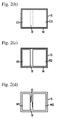
- Figs. 2(a) to 2(f) each of which is a plan view showing each step.
- the metal plates M1, M2 as circuit substrates and the metal plate M3 as a heat-dissipating plate were formed by basically the same steps in the production steps of the ceramic circuit substrate S described below, detailed explanation will be made only on the metal plates M1, M2, and the explanation of the metal plate M3 will be omitted.
- brazing material powder comprising 70.6% by mass of Ag, 2.9% by mass of In, and 1.9% by mass of Ti, the balance being Cu and residual amounts of impurities was mixed with 5.3 parts by mass of polyacrylate as an organic binder, 19.1 parts by mass of ⁇ -terpineol as an organic solvent, 0.5 parts by mass in total of polyoxyalkylene alkyl ether and alkyl benzenesulfonate as a dispersant, to prepare a brazing material paste. As shown in Fig.
- brazing regions c1, c2 both as thick as 40 ⁇ m were formed by the above brazing material paste on an upper surface (one surface) of the ceramic substrate S with a gap G in a planar direction by a screen printing method.
- the first brazing region c1 had a size of 27.6 mm and 11.6 mm in vertical and horizontal directions
- the second brazing region c2 had a size of 27.6 mm and 23.6 mm in vertical and horizontal directions, with a gap G of 1.0 mm between the brazing regions c1, c2.
- the brazing regions c1, c2 were covered with a metal plate M as thick as 0.5 mm, which was made of oxygen-free copper C1020H (JIS H3100), in the bonding step shown in Fig. 2(b) .
- a combination of the ceramic substrate S, the brazing regions c1, c2 and the metal plate M was heated in vacuum in a heating furnace, to bond the metal plate M to the ceramic substrate S via the brazing layers C1, C2, thereby providing the bonded body.
- the metal plate M used had a size of 29.5 mm and 39.5 mm in vertical and horizontal directions in Fig. 2(b) , smaller than the ceramic substrate S.
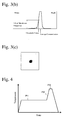
- the heating of the bonded body was conducted by a temperature pattern shown in Fig. 4 , which comprised a first temperature-keeping step P1 for keeping the bonded body at 400°C, the decomposition temperature of an acrylic resin as an organic binder, for 10 hours, and a second temperature-keeping step P3 for keeping the bonded body at 765°C, the melting point of the brazing material, for 1 hour, the second temperature-keeping step P3 being conducted after a temperature-ascending step P2 for heating the bonded body at a constant temperature-ascending speed after the first temperature-keeping step P1.
- two resist layers R1, R2 were formed in desired patterns on the metal plate M constituting the bonded body as shown in Fig. 2(c) , and then etched to remove unnecessary portions of the metal plate M, thereby forming two metal plates M1, M2, circuit patterns arranged with a gap G in a planar direction as shown in Fig. 2(d) .
- an ultraviolet-curable etching resist was formed in patterns corresponding to the first and second metal plates M1, M2 on the metal plate M by a screen printing method, and the resultant bonded body was immersed in an etching solution [ferric chloride (FeCl 3 ) solution (46.5 Be)] at 50°C, to form metal plates M1, M2.
- the first metal plate M1 had a size of 28 mm and 12 mm
- the second metal plate M2 had a size of 28 mm and 24 mm, both in vertical and horizontal directions.
- circuit-pattern-forming step and the brazing-material-removing step may be conducted after a cleaning step described below. However, to prevent the metal plates M1, M2 from being damaged, the circuit-pattern-forming step and the brazing-material-layer-removing step are conducted preferably between the bonding step and the cleaning step.
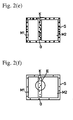
- the brazing-material-layer-removing step provided a bonded body having deposits K formed on the exposed surfaces of the ceramic substrate S, for example, as shown in Fig. 2(e) .
- This bonded body was cleaned with an aqueous sodium hypochlorite solution having the concentration and pH shown in Table 1, under the temperature and time conditions shown in Table 1.
- Fig. 2(f) most of the deposits K attached to the exposed surfaces of the ceramic substrate S were removed, resulting in a ceramic circuit substrate W with the deposits K remaining slightly.
- the sodium hypochlorite-containing agent used in the cleaning step was obtained by diluting an aqueous sodium hypochlorite solution having a concentration of 14.0% by mass, which was used in Example 16, with pure water, without particularly adjusting its pH.
- the bonded body after the cleaning step was immersed in an electroless plating solution (85°C) comprising nickel (Ni) as a main component and containing phosphorus (P) in a concentration of 8% by mass for 20-30 minutes, to form a Ni plating layer as thick as 5 ⁇ m on the metal (copper) substrates, thereby obtaining a ceramic circuit substrate.
- an electroless plating solution 85°C
- Ni nickel
- P phosphorus
- a ceramic circuit substrate was produced in the same manner as in Example 1, except for changing the cleaning agent, and the cleaning temperature and time as shown in Table 1.
- Comparative Example 1 a ceramic circuit substrate was produced in the same manner as in Example 1 except for omitting the cleaning step.
- a ceramic circuit substrate was produced in the same manner as in Example 1, except for using an aqueous solution comprising 3% by mass of hydrogen peroxide and 12% by mass of sulfuric acid as a cleaning agent in place of the aqueous sodium hypochlorite solution, with the cleaning temperature and time shown in Table 1.
- Example 1 Sodium Hypochlorite 2.0 9.2 30 10
- Example 2 Sodium Hypochlorite 2.5 9.5 30 10
- Example 3 Sodium Hypochlorite 3.0 9.8 30 10
- Example 4 Sodium Hypochlorite 5.0 10.4 30 10
- Example 5 Sodium Hypochlorite 7.0 10.9 30 10
- Example 6 Sodium Hypochlorite 8.0 11.2 30 10
- Example 7 Sodium Hypochlorite 9.0 11.5 30 10
- Example 8 Sodium Hypochlorite 10.0 11.8 30 10
- Example 9 Sodium Hypochlorite 12.0 12.3 30 10
- Example 10 Sodium Hypochlorite 13.0 12.9 40 40
- Example 11 Sodium Hypochlorite 13.0 12.9 45 50
- Example 12 Sodium Hypochlorite 13.0 12.9 50 60
- Example 13 Sodium Hypochlorite 13.0 12.9 60
- Example 14 Sodium Hypochlorite 13.0 12.9 30 10
- Example 15 Sodium Hypochlorite 13.5 13.1 30 10
- Example 16
- an optical photomicrograph of an exposed surface of the ceramic substrate S in the gap G in Fig. 2(g) was taken, and binarized to identify the deposits K.
- Pluralities of square regions F of 0.8 mm x 0.8 mm were set at arbitrary positions in each photomicrograph, and the area ratio of deposits K in each square region F was calculated, and averaged for all the square regions F.
- a threshold value of binarization was determined by obtaining the concentration distributions of deposits K on the binarized black-and-white images of several ceramic circuit substrates, and averaging them.
- Figs. 3(a) to 3(c) The method of determining a threshold value used for obtaining a monochromatic image of the deposits K will be explained in detail below referring to Figs. 3(a) to 3(c) .
- a portion including a deposit K was cut out of the optical photomicrograph [ Fig. 3(a) ], and a concentration therein was divided to 256 steps.
- the resultant concentration distribution was depicted in Fig. 3(b) , in which the axis of abscissa indicates the concentration, and the axis of ordinate indicates a frequency.
- a concentration at the maximum frequency was an average concentration
- a concentration at a half of the maximum frequency was a threshold value, in this ceramic circuit substrate. Threshold values were similarly determined on other ceramic circuit substrates.
- the threshold values of all the ceramic circuit substrates were averaged to determine a threshold value for binarization.
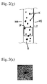
- the image of a deposit K in Fig. 3(a) was binarized using this threshold value to obtain a binarized image shown in Fig. 3(c) . It was confirmed by energy-dispersive X-ray spectrometer (UTW-type Si (Li) semiconductor detector with beam diameter of 1 nm available from Nolan Instruments Co., Ltd.) that black portions in Fig. 2(g) were carbonaceous deposits K.
- the insulation breakdown voltage was measured by applying AC voltage between front and back surfaces of the ceramic circuit substrate.
- electrically short-circuited spherical electrodes A and B were disposed on the first and second metal plates M1, M2, and an electrode C (not shown) was attached to the metal plate M3 on a back surface of the ceramic circuit substrate.
- This ceramic circuit substrate was set in an insulating silicone oil at room temperature, and alternating voltage of 0-10 kV gradually increasing at a speed of 0.1 kV/sec was applied between front and back surfaces of the circuit substrate in a withstand voltage tester (TOS5101 available from Kikusui Electronics Corporation), to measure, as insulation breakdown voltage, voltage at which current exceeding the upper limit of leak current flew. This measurement was conducted on five samples, and the resultant measured values were averaged.
- TOS5101 available from Kikusui Electronics Corporation
- the ceramic substrate for this test piece was obtained by producing a silicon nitride substrate with no circuit pattern, and subjecting the silicon nitride substrate to the same chemical treatment as that of the ceramic circuit substrate without copper bonding. Namely, by measuring the bending strength of the test piece, the strength variation of the silicon nitride substrate was measured.
- a sensor used was a load cell (SBL-1kN). The average bending strength was determined by averaging the values measured on 10 test pieces.
- Example 1 (1) 0.82 2.8 7.7 776
- Example 2 (1) 0.77 3.2 7.9 772
- Example 3 0.55 8.8 8.1 788
- Example 4 0.42 13 7.8 769
- Example 5 0.33 25 8.0 789
- Example 6 0.31 32 8.5 774
- Example 8 0.18 88 8.6 771
- Example 9 0.13 110 8.7 761
- Example 10 0.05 540 8.8 775
- Example 11 0.04 650 8.9 782
- Example 12 0.03 725 8.9 769
- Example 13 0.02 784 9.3 773
- Example 14 0.08 180 9.0 790
- Example 16 0.04 250 8.9 785
- Example 17 0.47 9.9 7.9 791
- Example 18 0.41 13 7.7 783
- Example 19 0.39 15 8.1 767
- Example 20 0.37 19 8.4 781
- Example 21 0.34 24 8.3 792
- Example 22 0.37 17 8.1 785
- the area ratio of deposits K on the ceramic substrate surfaces exposed in a gap G between two metal plates M1, M2 was 10% or less, with the minimum insulation resistance of 500 M ⁇ /mm or more between the metal plates M1, M2.
- the area ratio of deposits K was as large as 17.6%, the minimum insulation resistance was as extremely low as 0.4 x 10 3 M ⁇ /mm, and the insulation breakdown voltage was as low as 6.2 kV. This appears to be due to the fact that the ceramic circuit substrate of Comparative Example 1 suffered large variations of measured insulation resistance and a large area ratio of deposits K. Further, breakdown much occurred on the surfaces.
- Examples 1-9 and 14-16 in which the concentration of a cleaning agent (aqueous sodium hypochlorite solution) varied from 2.0% by mass to 14.0% by mass (pH 9.2-13.2) with constant cleaning time and temperature, revealed that a higher concentration (pH) of the aqueous sodium hypochlorite solution provided a lower area ratio of deposits K, and a larger minimum insulation resistance.
- the ceramic circuit substrates of Examples 1 and 2 had area ratios of deposits K of 0.82% and 0.77%, respectively, slightly higher than those of Examples 3-9 and 14-16, with surface insulation breakdown observed. This appears to be due to the fact that the cleaning agent (aqueous sodium hypochlorite solution) had pH as relatively low as 9.2 and 9.5.
- Example 15 using an aqueous sodium hypochlorite solution having pH of 13.1 and Example 16 using an aqueous sodium hypochlorite solution having pH of 13.2 the area ratios of deposits K were as long as 0.05% and 0.04%, and the minimum insulation resistances were as large as 210 x 10 3 M ⁇ /mm and 250 x 10 3 M ⁇ /mm.
- the cleaning step in Examples 1-30 did not damage the function as electrodes of the metal plates M1, M2 in each sample.
- Deposits derived from a brazing material paste, etc. are removed or decreased by cleaning the bonded body with a hypochlorite-containing agent, providing a ceramic circuit substrate having excellent electric insulation between metal plates with no appearance defects.
Landscapes
- Chemical & Material Sciences (AREA)
- Engineering & Computer Science (AREA)
- Materials Engineering (AREA)
- Mechanical Engineering (AREA)
- Organic Chemistry (AREA)
- Metallurgy (AREA)
- General Chemical & Material Sciences (AREA)
- Chemical Kinetics & Catalysis (AREA)
- Ceramic Engineering (AREA)
- Manufacturing & Machinery (AREA)
- Microelectronics & Electronic Packaging (AREA)
- Structural Engineering (AREA)
- Manufacturing Of Printed Wiring (AREA)
- Manufacturing Of Printed Circuit Boards (AREA)
Description
- The present invention relates to a method for producing a ceramic circuit substrate comprising a ceramic substrate, brazing layers formed on the ceramic substrate, and metal plates bonded to the ceramic substrate via the brazing layers, and a ceramic circuit substrate having the structure.
- The production method of a ceramic circuit substrate, which may be called simply "circuit substrate" below, by brazing is disclosed, for example, in
JP 2003-110222 A JP 2003-110222 A - More specifically, the production method of a circuit substrate disclosed in
JP 2003-110222 A - As described above, in the production of a circuit substrate by a brazing method, a method comprising the steps of applying a brazing material paste comprising brazing material powder and an organic binder to a ceramic substrate, setting metal plates in contact with the brazing material paste to form a bonded body comprising the ceramic substrate, the brazing material paste and the metal plates, heating the bonded body at a brazing-material-melting temperature in vacuum or in non-oxidizing state to bond the metal plates to the ceramic substrate via the brazing material is widely used. The organic binder contained in the brazing material paste is decomposed and gasified in the heating process of the bonded body, so that it is removed from the brazing material paste. However, part of the gasified organic binder is likely deposited onto exposed surfaces of the ceramic substrate, which are not covered with the metal plates, forming carbon-based adhesive deposits. In the heating of the bonded body, deposits from a heating furnace atmosphere, etc. may also be formed on the bonded body.
- Such deposits attached to the ceramic substrate surface are black or gray, evidently different from the color of the ceramic substrate, thereby being treated as defects in appearances. Also, because many of the deposits are highly conductive, sufficient electric insulation is unlikely secured between two metal plates constituting the metal circuit substrate, when large amounts of deposits are attached to the ceramic substrate surfaces exposed in a gap between the two metal plates, providing the circuit substrate with insulation resistance defects. It is extremely difficult to remove the insulation-resistance-decreasing deposits strongly attached to the ceramic substrate surface, by the etching solution or brazing-material-removing liquid disclosed in
JP 2003-110222 A - Accordingly, an object of the present invention is to provide a method for producing a ceramic circuit substrate with insulation-resistance-decreasing deposits removed or decreased on ceramic-substrate-exposed surfaces, and such a ceramic circuit substrate.
- As a result of intensive research in view of the above object, it has been found that by brazing metal plates to a ceramic substrate via a brazing material, and cleaning the bonded body with a hypochlorite-containing agent, insulation-resistance-decreasing deposits derived from a brazing material paste, etc. are removed or decreased in a ceramic circuit substrate. The present invention has been completed based on such finding.
- Thus, the method of the present invention for producing a ceramic circuit substrate comprises the steps of
forming brazing regions each comprising brazing material powder and an organic binder on a ceramic substrate;
setting metal plates on the ceramic substrate via the brazing regions, and heating the ceramic substrate, the brazing regions and the metal plates to bond the metal plates to the ceramic substrate via brazing layers made of the brazing material, thereby forming a bonded body; and
cleaning the bonded body with a hypochlorite-containing agent. - It is preferable that a resist layer is formed on the metal plates after the bonding step and before the cleaning step; that the metal plates are etched to form circuit patterns; and that residual brazing layers are then removed.
- The concentration of hypochlorite in the agent is preferably 2.5-13.5% by mass as sodium hypochlorite. The agent preferably has pH of 9 or more.
- The cleaning is preferably conducted at 30°C or higher for 5 minutes or more.
- The ceramic circuit substrate of the present invention comprises a ceramic substrate, two brazing layers formed on the ceramic substrate, and two metal plates each bonded to each of the two brazing layers; insulation resistance between the two metal plates being 500 MΩ/mm or more; and the area ratio of insulation-resistance-decreasing deposits on the ceramic substrate surfaces exposed in a gap between the two metal plates being 15% or less.
- On the ceramic substrate surfaces exposed in a gap between the two metal plates, the density of deposits having the maximum diameter of 50 µm or more is preferably 50/mm2 or less.
- The ceramic substrate is preferably composed of a sintered nitride ceramic comprising a main phase of silicon-nitride-based or aluminum-nitride-based grains, and a grain boundary phase based on sintering aids between the grains, pores existing on ceramic substrate surfaces exposed in a gap between the two metal plates having the maximum diameter of 2-15 µm.
-
-
Fig. 1(a) is a front view schematically showing a ceramic circuit substrate. -
Fig. 1(b) is a plan view ofFig. 1(a) . -
Fig. 2(a) is a first plan view for explaining a method for producing the ceramic circuit substrate ofFig. 1(a) . -
Fig. 2(b) is a second plan view for explaining the method for producing the ceramic circuit substrate ofFig. 1(a) . -
Fig. 2(c) is a third plan view for explaining the method for producing the ceramic circuit substrate ofFig. 1(a) . -
Fig. 2(d) is a fourth plan view for explaining the method for producing the ceramic circuit substrate ofFig. 1(a) . -
Fig. 2(e) is a fifth plan view for explaining the method for producing the ceramic circuit substrate ofFig. 1(a) . -
Fig. 2(f) is a sixth plan view for explaining the method for producing the ceramic circuit substrate ofFig. 1(a) . -
Fig. 2(g) is an enlarged view showing a portion E inFig. 2(f) . -
Fig. 3(a) is an optical photomicrograph showing a carbonaceous deposit existing in a gap in the circuit substrate. -
Fig. 3(b) is a graph (histogram) showing a black-and-white concentration distribution of carbonaceous deposits, which is determined from the image ofFig. 3(a) . -
Fig. 3(c) is an image obtained by binarizing the image ofFig. 3(a) using one-half of the maximum concentration as a threshold value. -
Fig. 4 is a graph showing a temperature profile in the bonding step. -
Fig. 5(a) is a photograph showing a cross section of the ceramic substrate of Example 9. -
Fig. 5(b) is a photograph showing a cross section of the ceramic substrate of Comparative Example 2. - The method of the present invention for producing a ceramic circuit substrate comprises the steps of (a) forming brazing regions each comprising brazing material powder and an organic binder on a ceramic substrate; (b) heating the ceramic substrate, the brazing regions, and metal plates placed on the ceramic substrate via the brazing regions, to bond the metal plates to the ceramic substrate via brazing layers made of the brazing material, thereby forming a bonded body; and (c) cleaning the bonded body with a hypochlorite-containing agent.
- Brazing regions each comprising brazing material powder and an organic binder are formed on a ceramic substrate. The brazing material includes metal powder comprising Ag, Cu, etc. in a predetermined composition, and various organic resins may be used as the organic binder. The brazing regions may be formed by coating the ceramic substrate with a brazing material paste comprising brazing material powder and an organic binder by such a method as screen printing, etc.
- When an acrylic resin is used as a binder in the brazing material paste, deposits formed by a gasified acrylic resin are likely formed on the ceramic substrate surface, in the heating process for bonding the metal plates to the ceramic substrate via the brazing material. Accordingly, when the acrylic resin is used as the binder, the method of the present invention exhibits more effects of removing or decreasing the deposits. The acrylic resin may be polyacrylate or polymethacrylate.
- The ceramic substrate, the brazing regions comprising the brazing material powder and the organic binder, which are formed on the ceramic substrate, and the metal plates set via the brazing regions are heated to bond the metal plates to the ceramic substrate via the brazing layers. Heating is preferably conducted in vacuum or in a reducing atmosphere, with the temperature once kept at around a binder-decomposing temperature (for example, around 400°C) to decompose and remove the organic component in the brazing material paste, and then kept at the brazing temperature for 10 minutes or more, in a temperature-ascending process. The brazing temperature is a temperature at which brazing layers can be properly formed, namely, a temperature equal to or higher than the melting point of the brazing material. The brazing temperature is usually the highest temperature in the temperature-ascending process.
- A lower keeping temperature for decomposing and removing the binder tends to make carbon remain without being sufficiently removed. Accordingly, the keeping temperature for decomposing and removing the binder is preferably 300°C or higher. For example, in the case of a binder including an acrylic resin, this keeping temperature is preferably 360°C or higher. To prevent active metals in the brazing material from being oxidized by oxygen contained in the resin, etc. in the binder, the keeping temperature for decomposing and removing the binder is preferably 500°C or lower, more preferably 480°C or lower.
- For example, an Ag-Cu-based brazing material having a melting point of 770-880°C is preferably used as the brazing material at a brazing temperature of 770-880°C. The temperature of 770°C or higher sufficiently melts the brazing material, preventing the formation of voids. It is more preferably 790°C or higher. Excessive wetting with the brazing material does not spread at 880°C or lower. The brazing temperature is more preferably 830-870°C. Though the brazing-temperature-keeping time depends on the amount charged into a heating furnace for bonding, it is preferably within 5 hours, more preferably within 2 hours, from the aspect of productivity. The brazing-temperature-keeping time may be properly set depending on the number of samples, and depending on the volume of a heating furnace for bonding and the displacement of a vacuum pump, for example, in the case of using a vacuum atmosphere. In order that the metal plates are bonded to the ceramic substrate without voids, heating is preferably conducted under load.
- In the bonding step, the organic binder contained in the decomposed brazing material may be deposited on part of the ceramic substrate surface, which is not covered with the metal plates, namely, on the exposed surfaces of the ceramic substrate. To remove deposits of this organic binder, cleaning is conducted with a hypochlorite-containing agent.
- The hypochlorite may be preferably sodium hypochlorite, potassium hypochlorite, calcium hypochlorite, etc., more preferably sodium hypochlorite, calcium hypochlorite, or a mixture of sodium hypochlorite and calcium hypochlorite, particularly sodium hypochlorite.
- The hypochlorite-containing agent is a solution of hypochlorite in water (pure water), in an organic solvent or in a mixture of water and an organic solvent. Instead of using hypochlorite, an aqueous hypochloric acid solution may be hydrolyzed with a base (sodium hydroxide, etc.) to have pH of 9 or more. A solution of hypochlorite in water (pure water) is usually used. The solution may contain an anticorrosion agent, a stabilizer, additives, a pH adjuster, etc., if necessary.
- Because the effect of removing deposits is larger as the concentration of hypochlorite ions (ClO-) in the agent is higher, hypochloric acid should be sufficiently hydrolyzed (dissociated). To this end, the pH of the agent is preferably 9-13, when an alkali salt such as hypochlorite of potassium, calcium, sodium, etc. is used. When the pH of the agent is less than 9, the hydrolysis of hypochloric acid is insufficient, resulting in a low concentration of hypochlorite ions (ClO-), and low capacity of removing deposits formed on the ceramic substrate surface, thus consuming a lot of time. Though higher pH provides a more rapid removal reaction of deposits, the pH is preferably up to about 13 to achieve a stable, uniform reaction. Also, the pH of more than 13 is undesirable for handling because of extremely increased danger. Namely, the pH of the agent is more preferably 9.5-13, most preferably 10-13. For example, when sodium hypochlorite is used, its concentration may be adjusted to obtain pH of 9-13, but it is preferable to adjust the pH by adding an alkali such as sodium hydroxide, potassium hydroxide, ammonia water, etc. as a pH adjuster. A buffer may be used if necessary.
- The concentration of hypochlorite such as potassium hypochlorite, calcium hypochlorite, sodium hypochlorite, etc. in the agent is preferably 2.5-13.5% by mass, more preferably 8-13% by mass, when calculated as sodium hypochlorite. "Concentration when calculated as sodium hypochlorite" means a concentration determined when a counter salt (K+, Ca2+, Na+, etc.) of hypochlorite ions is substituted by sodium (Na+) while keeping the same equivalent concentration. For example, 5% by mass of calcium hypochlorite [Ca(ClO)2, molecular weight: 142.98, gram equivalent: 71.49] is equivalent to 5.42% by mass of sodium hypochlorite [NaClO, molecular weight: 77.44, gram equivalent: 77.44], by the calculation of 5% by mass x 77.44/71.49 = 5.42% by mass.
- To obtain a sufficient cleaning effect when hypochlorite is used, one or more of KOH, NH3 and NaOH as a pH adjuster is preferably added to adjust the pH range. For example, in a diluted sodium hypochlorite solution (pH: 8-10), hypochloric acid exists mainly as dissociated OCl-. On the other hand, in an aqueous hypochloric acid solution in a pH range including a strong acid range (pH ≤ 2.7) and a mild acid range (pH: 5.0-6.5), hypochloric acid exists as undissociated HOCl in an extremely high percentage. To exhibit a high effect of cleaning carbonaceous deposits, etc. existing on the substrate surface, undissociated HOCl should be converted to dissociated OCl- by hydrolysis with a base.
- When the agent adjusted as described above is used in the cleaning step, cleaning the bonded body at 30°C or higher for 5 minutes or more is desirable to exhibit a higher effect of removing deposits from the ceramic substrate surface. When the cleaning temperature exceeds 60°C, sodium hypochlorite is decomposed to sodium chloride and sodium hydroxide, resulting in a shorter solution life. Further, the agent is made strongly alkaline, corroding not only the metal plates but also grain boundary phases exposed on the ceramic substrate surface. Accordingly, the cleaning temperature is preferably 60°C or lower. From the aspect of suppressing the corrosion of the metal plates, the cleaning time is preferably 60 minutes or less.
- Though not particularly restrictive, the organic solvent is preferably a water-soluble organic solvent, including alcohols such as methanol, ethanol, n-propanol, 2-propanol, n-butanol, sec-butanol, tert-butanol, etc.; diols such as ethylene glycol, propylene glycol, 1,3-propanediol, 1,2-butanediol, 2,3-butanediol, 1,3-butanediol, 1,4-butanediol, etc.; ether alcohols such as ethylene glycol monomethyl ether, ethylene glycol monoethyl ether, ethylene glycol monoisopropyl ether, ethylene glycol monobutyl ether, diethylene glycol monomethyl ether, diethylene glycol monoethyl ether, diethylene glycol monoisopropyl ether, diethylene glycol monobutyl ether, propylene glycol monomethyl ether, propylene glycol monoethyl ether, dipropylene glycol monomethyl ether, dipropylene glycol monoethyl ether, etc.; amides such as formamide, N-methylformamide, N,N-dimethylformamide, N,N-diethyl formamide, acetamide, N-methylacetamide, N,N-dimethylacetamide, N-methylpropionamide, 2-pyrrolidone, N-methylpyrrolidone, etc.; dimethyl sulfoxide; sulfolane; etc. They may be used alone or in combination.
- The anticorrosion agent includes, for example, saccharides or sugar alcohols such as glucose, mannose, galactose, sorbitol, mannitol, xylitol, etc.; aromatic hydroxyl compounds such as phenol, cresol, catechol, resorcin, 2,3-pyridinediol, pyrogallol, salicylic acid, gallic acid, etc.; alkyne alcohols such as 3-methyl-1-butyne-3-ol, 3-methyl-1-pentyne-3-ol, 3,6-dimethyl-4-octyne-3,6-diol, 2,4,7,9-tetramethyl-5-decyne-4,7-diol, 3,5-dimethyl-1-hexyne-3-ol, 2-butyne-1,4-diol, etc.; triazoles such as benzotriazole, o-tolyltriazole, m-tolyltriazole, p-tolyltriazole, carboxy benzotriazole, 1-hydroxybenzotriazole, nitrobenzotriazole, dihydroxypropyl benzotriazole, etc. They may be used alone or in combination.
- The additives include various surfactants, chelating agents, defoamers, etc. They may be added alone or in combination. The surfactants include, for example, polyoxyethylene lauryl ether, polyoxyethylene stearyl ether, monoethanolamine, triethanolamine, etc. The chelating agents include, for example, ethylenedimine, etc. The defoamers include, for example, polyoxyalkylene alkyl ether, polyoxyethylenealkylene ether, and silicone agents, etc.
- Before the bonding step and after the cleaning step, (d1) a step of forming a circuit patterns by forming resist layers on the metal plates in a pattern along a periphery of each brazing layer formed by the bonding step, and etching the metal plates, and (d2) a step of removing residual brazing layers after the formation of the circuit patterns are preferably conducted. After the circuit-pattern-forming step and the brazing-material-removing step, the above cleaning step can be conducted to remove deposits formed on the ceramic substrate in the circuit-pattern-forming step and/or the brazing-material-layer-removing step. Thus, a subsequent cleaning step enables the formation of the circuit patterns and the removal of the brazing material to be conducted under the optimum conditions without suffering the formation of deposits, thereby reducing damage in the resist layers and the metal plates in both steps. The resist layers are preferably formed in patterns along peripheries of the brazing layers formed in the bonding step.
- For such reasons, the resist layers formed in the circuit-pattern-forming step can be as thin as 10-80 µm, preferably 30-70 µm.
- The resist layers are preferably made of an ultraviolet-curable resist agent. The ultraviolet-curable resist agent includes copolymeric acrylate oligomers, acrylate monomers, fillers, photopolymerization initiators, color-adjusting agents, and defoaming/leveling agents. A copolymeric acrylate oligomer, a main component of the ultraviolet-curable resist agent, is a high-viscosity polymer hardenable by a condensation polymerization reaction. The copolymeric acrylate oligomer as a main component includes epoxy acrylates, urethane acrylates, polyester acrylates, polyether acrylates, and other copolymers. Acrylate monomers include isoamyl acrylate, lauryl acrylate, stearyl acrylate, ethoxydiethylene glycol acrylate, 2-hydroxyethyl acrylate, phenoxyethyl acrylate, etc.
- The ultraviolet-curable resist agent is polymerized with an acrylate monomer by a radical reaction using a photopolymerization initiator, and its chemical resistance to an etching solution and a brazing-material-removing liquid can be improved by the degree of polymerization of the resultant copolymeric acrylate oligomer. The acrylate monomer constitutes a skeleton of the cured resist layer, providing the resist layer with improved flexibility and high adhesion to a circuit substrate. In a paste-like ultraviolet-curable resist agent before curing, the acrylate monomer functions as a viscosity-adjusting agent for providing fluidity.
- For example, when a liquid agent comprising hydrogen peroxide and acidic ammonium fluoride is used as a brazing-material-removing liquid, a brazing-material-removing liquid comprising 10-40% by mass of hydrogen peroxide and 1-8% by mass of acidic ammonium fluoride can be used. Less than 10% by mass of hydrogen peroxide provides insufficient capability of removing the brazing material, and more than 40% by mass of hydrogen peroxide excessively corrodes the metal plates, resulting in poor dimensional precision of the metal plates. Less than 1% by mass of acidic ammonium fluoride provides a reduced capability of removing a reaction layer containing active metals, which is formed in a bonding interface between the brazing layers and the ceramic substrate. On the other hand, more than 8% by mass of acidic ammonium fluoride dissolves crystal grains in the ceramic substrate, deteriorating electric insulation and strength required for the ceramic substrate.
- A step of forming plating layers of Ni, Au, etc. on the metal plates may be further conducted. For example, Ni plating layers as thick as about 5 µm can be formed on the metal plates, by immersing the metal plates in an electroless plating solution (85°C) comprising nickel (Ni) as a main component and phosphorus (P) in a concentration adjusted to 8% by mass, for 20-30 minutes. Before the plating step, a chemical grinding step of the metal plates may be conducted, if necessary.
- The circuit substrate of the present invention is a ceramic circuit substrate comprising a ceramic substrate, two brazing layers formed with a gap therebetween on the ceramic substrate, and two metal plates bonded to the ceramic substrate via the two brazing layers, insulation resistance between the two metal plates being 500 MΩ/mm or more. The number of the brazing layers and the number of the bonded metal plates are not restricted to 2, but may be 3 or more. In that case, three or more metal plates may be bonded. With insulation resistance of 500 MΩ/mm or more between the two metal plates in a ceramic circuit substrate comprising semiconductor devices mounted on the two metal plates, even excessive current does not break insulation between the two metal plates, so that it does not flow through the semiconductor devices. The ceramic circuit substrate of the present invention is preferably produced by the above method of the present invention.
- The ceramic circuit substrate having as high insulation resistance as described above can be produced, for example, by limiting the area ratio of deposits on the ceramic substrate surfaces exposed in a gap between the two metal plates to preferably 15% or less, more preferably 10% or less. Further, high-conductive deposits on the ceramic substrate surfaces exposed in a gap between the two metal plates tend to be networked to cause insulation breakdown. The networking of the deposits can be suppressed by limiting the density of deposits having the maximum diameter of 50 µm or more to 50/mm2 or less.
- When the ceramic substrate is a sintered nitride ceramic comprising a main phase of silicon-nitride-based grains or aluminum-nitride-based grains, and a grain boundary phase based on sintering aids between the grains, the maximum diameter of pores in the ceramic substrate in the gap is preferably 2-15 µm. When the maximum diameter of the pores is less than 2 µm, the deposits may not be sufficiently removed by the agent in the cleaning step. On the other hand, when the maximum diameter of the pores is more than 15 µm, the ceramic substrate has low strength, so that the ceramic circuit substrate is less reliable, for example, in the cooling cycle.
-
Figs. 1(a) and 1(b) are respectively a front view and an upper plan view showing an example of the ceramic circuit substrates of the present invention. The ceramic circuit substrate W is basically constituted by a ceramic substrate S; twobrazing layers C 1, C2 formed via a gap G on an upper surface (one surface) of the ceramic substrate S, which may be called "first brazing layer C1" and "second brazing layer C2" below; and two metal plates M1, M2 each bonded to an upper surface of the ceramic substrate S via each of the two brazing layers C1, C2, and acting as a circuit substrate on which semiconductor devices, etc. are mounted, which may be called "first metal plate M1" and "second metal plate M2" below. Each of the two metal plates M1, M2 is provided with a plating layer of Ni, Au, etc. The ceramic circuit substrate W shown inFigs. 1(a) and 1(b) comprises a metal plate M3 bonded to a lower surface (the other surface) of the ceramic substrate S via a brazing layer C3 to act as a heat-dissipating plate. - In the present invention characterized by removing deposits from the exposed surfaces of the ceramic substrate S, materials for the ceramic substrate S used in the ceramic circuit substrate W are not particularly restricted, but may be basically a sintered body of electrically insulating materials. However, because semiconductor devices mounted on the ceramic circuit substrate W have recently become higher in operation frequencies, generating larger heat, the ceramic substrate S is preferably made of nitride ceramics having high thermal conductivity. Specifically, the ceramic substrate S is preferably made of sintered aluminum nitride comprising a main phase of aluminum-nitride-based grains and a grain boundary phase based on sintering aids between the grains, or sintered silicon nitride comprising a main phase of silicon-nitride-based grains and a grain boundary phase based on sintering aids between the grains. More preferably, the ceramic substrate S is made of sintered silicon nitride having excellent mechanical strength and fracture toughness.
- Because the ceramic substrate S of sintered silicon nitride tends to have larger surface roughness due to the influence of columnar grains, in a heating process, in which the ceramic substrate is bonded to the metal plates via a brazing material paste comprising brazing material powder and an organic binder, deposits of a gasified organic binder are likely formed on the rough ceramic surfaces. Accordingly, in the case of using a ceramic substrate S of sintered silicon nitride, the method of the present invention for producing a ceramic circuit substrate exhibits high effects of removing or decreasing the deposits.
- When the ceramic substrate S is made of sintered silicon nitride, for example, starting material powder comprising 90-97% by mass of silicon nitride, and 3-10% by mass of a sintering aid including Mg and Y (and other rare earth elements) is mixed with proper amounts of an organic binder, a plasticizer, a dispersant and an organic solvent by ball milling, etc. to form slurry, and this slurry is formed into a thin ceramic green sheet by a doctor blade method or a calendar roll method. The ceramic green sheet is punched or cut to a desired shape, and sintered at a temperature of 1700-1900°C to obtain the ceramic substrate S.
- Materials for the metal plates M1-M3 constituting the ceramic circuit substrate W are not particularly restricted, as long as they can be bonded by a brazing material and have a higher melting point than that of the brazing material. The metal plates can be made of, for example, copper or its alloys, aluminum or its alloys, silver or its alloys, nickel or its alloys, nickel-plated molybdenum, nickel-plated tungsten, or nickel-plated iron alloys. Among them, copper or copper-containing alloys are most preferable from the aspect of electric resistance and elongation, as well as for high thermal conductivity (low thermal resistance), low migration, etc. Aluminum or aluminum-containing alloys are preferable in mounting reliability due to plastic deformation in a heating/cooling cycle, despite higher electric resistance and lower thermal conductivity (higher thermal resistance) than those of copper.
- Materials for the brazing layers C1-C3 bonding the metal plates M1-M3 to the ceramic substrate S are not particularly restricted, but may be preferably an Ag-Cu-based active brazing material comprising a main phase having a eutectic composition of Ag and Cu for exhibiting high strength, high sealability, etc., and an active metal of Ti, Zr, Hf, etc. From the aspect of bonding strength of the metal plates M1-M3 to the ceramic substrate S, an Ag-Cu-In-based, active brazing material, a ternary system obtained by adding In to the Ag-Cu-based, active brazing material, is more preferable. The bonding of the metal plates to the ceramic substrate S is conducted, as described above, by using a brazing material paste comprising powders of the brazing material components and an organic binder.
- The present invention will be explained in further detail by Examples below, without intention of restricting the present invention thereto.
- As shown in
Figs. 1(a) and 1(b) , a ceramic circuit substrate W comprising a ceramic substrate S; two brazing layers C1, C2 formed on an upper surface (one surface) of the ceramic substrate S via a gap G, which may be called "first brazing layer C1" and "second brazing layers C2" below; two metal plates M1, M2 each bonded to an upper surface of the ceramic substrate S via each brazing layer C1, C2, which may be called "first metal plate M1" and "second metal plate M2" below; a Ni plating layer formed on each metal plate M1, M2; and a metal plate M3 bonded to a lower surface (the other surface) of the ceramic substrate S via a brazing layer C3 was produced by the method described below. - A ceramic substrate S of 30 mm and 40 mm in vertical and horizontal directions, and 0.32 mm in thickness in
Fig. 1(b) was made of silicon nitride comprising 93% by mass of Si3N4, 4% by mass of Mg as converted to the amount of its oxide, and 3% by mass of Y as converted to the amount of its oxide, the total amount of the starting material powders being 100 parts by mass. - Each step in the production method of the ceramic circuit substrate S will be explained below referring to
Figs. 2(a) to 2(f) , each of which is a plan view showing each step. Because the metal plates M1, M2 as circuit substrates and the metal plate M3 as a heat-dissipating plate were formed by basically the same steps in the production steps of the ceramic circuit substrate S described below, detailed explanation will be made only on the metal plates M1, M2, and the explanation of the metal plate M3 will be omitted. - 100 parts by mass of a brazing material powder comprising 70.6% by mass of Ag, 2.9% by mass of In, and 1.9% by mass of Ti, the balance being Cu and residual amounts of impurities was mixed with 5.3 parts by mass of polyacrylate as an organic binder, 19.1 parts by mass of α-terpineol as an organic solvent, 0.5 parts by mass in total of polyoxyalkylene alkyl ether and alkyl benzenesulfonate as a dispersant, to prepare a brazing material paste. As shown in
Fig. 2(a) , two brazing regions c1, c2 both as thick as 40 µm were formed by the above brazing material paste on an upper surface (one surface) of the ceramic substrate S with a gap G in a planar direction by a screen printing method. InFig. 2(a) , the first brazing region c1 had a size of 27.6 mm and 11.6 mm in vertical and horizontal directions, and the second brazing region c2 had a size of 27.6 mm and 23.6 mm in vertical and horizontal directions, with a gap G of 1.0 mm between the brazing regions c1, c2. - After the formation of the brazing regions, the brazing regions c1, c2 were covered with a metal plate M as thick as 0.5 mm, which was made of oxygen-free copper C1020H (JIS H3100), in the bonding step shown in
Fig. 2(b) . A combination of the ceramic substrate S, the brazing regions c1, c2 and the metal plate M was heated in vacuum in a heating furnace, to bond the metal plate M to the ceramic substrate S via the brazing layers C1, C2, thereby providing the bonded body. Taking into consideration the thermal expansion of the metal plate M in the bonding step, the metal plate M used had a size of 29.5 mm and 39.5 mm in vertical and horizontal directions inFig. 2(b) , smaller than the ceramic substrate S. - The heating of the bonded body was conducted by a temperature pattern shown in
Fig. 4 , which comprised a first temperature-keeping step P1 for keeping the bonded body at 400°C, the decomposition temperature of an acrylic resin as an organic binder, for 10 hours, and a second temperature-keeping step P3 for keeping the bonded body at 765°C, the melting point of the brazing material, for 1 hour, the second temperature-keeping step P3 being conducted after a temperature-ascending step P2 for heating the bonded body at a constant temperature-ascending speed after the first temperature-keeping step P1. - After the bonding step, two resist layers R1, R2 were formed in desired patterns on the metal plate M constituting the bonded body as shown in
Fig. 2(c) , and then etched to remove unnecessary portions of the metal plate M, thereby forming two metal plates M1, M2, circuit patterns arranged with a gap G in a planar direction as shown inFig. 2(d) . Specifically, an ultraviolet-curable etching resist was formed in patterns corresponding to the first and second metal plates M1, M2 on the metal plate M by a screen printing method, and the resultant bonded body was immersed in an etching solution [ferric chloride (FeCl3) solution (46.5 Be)] at 50°C, to form metal plates M1, M2. InFig. 2(d) , the first metal plate M1 had a size of 28 mm and 12 mm, and the second metal plate M2 had a size of 28 mm and 24 mm, both in vertical and horizontal directions. - As shown in
Fig. 2(d) , after the resist layers were removed from the metal plates M1, M2, residual brazing material layers D flowing out from peripheries of the metal plates M1, M2 were removed by a brazing-material-removing liquid comprising 26% by mass of hydrogen peroxide and acidic ammonium fluoride at 40°C for 40 minutes. The circuit-pattern-forming step and the brazing-material-removing step may be conducted after a cleaning step described below. However, to prevent the metal plates M1, M2 from being damaged, the circuit-pattern-forming step and the brazing-material-layer-removing step are conducted preferably between the bonding step and the cleaning step. - The brazing-material-layer-removing step provided a bonded body having deposits K formed on the exposed surfaces of the ceramic substrate S, for example, as shown in
Fig. 2(e) . Analysis indicated that most of the deposits K were carbonaceous. This bonded body was cleaned with an aqueous sodium hypochlorite solution having the concentration and pH shown in Table 1, under the temperature and time conditions shown in Table 1. As a result, as shown inFig. 2(f) , most of the deposits K attached to the exposed surfaces of the ceramic substrate S were removed, resulting in a ceramic circuit substrate W with the deposits K remaining slightly. The sodium hypochlorite-containing agent used in the cleaning step was obtained by diluting an aqueous sodium hypochlorite solution having a concentration of 14.0% by mass, which was used in Example 16, with pure water, without particularly adjusting its pH. - The bonded body after the cleaning step was immersed in an electroless plating solution (85°C) comprising nickel (Ni) as a main component and containing phosphorus (P) in a concentration of 8% by mass for 20-30 minutes, to form a Ni plating layer as thick as 5 µm on the metal (copper) substrates, thereby obtaining a ceramic circuit substrate.
- A ceramic circuit substrate was produced in the same manner as in Example 1, except for changing the cleaning agent, and the cleaning temperature and time as shown in Table 1.
- In Comparative Example 1, a ceramic circuit substrate was produced in the same manner as in Example 1 except for omitting the cleaning step. In Comparative Example 2, a ceramic circuit substrate was produced in the same manner as in Example 1, except for using an aqueous solution comprising 3% by mass of hydrogen peroxide and 12% by mass of sulfuric acid as a cleaning agent in place of the aqueous sodium hypochlorite solution, with the cleaning temperature and time shown in Table 1.
Table 1 No. Cleaning Step Agent Temperature (°C) Time (minutes) Component Concentration (% by mass) pH Example 1 Sodium Hypochlorite 2.0 9.2 30 10 Example 2 Sodium Hypochlorite 2.5 9.5 30 10 Example 3 Sodium Hypochlorite 3.0 9.8 30 10 Example 4 Sodium Hypochlorite 5.0 10.4 30 10 Example 5 Sodium Hypochlorite 7.0 10.9 30 10 Example 6 Sodium Hypochlorite 8.0 11.2 30 10 Example 7 Sodium Hypochlorite 9.0 11.5 30 10 Example 8 Sodium Hypochlorite 10.0 11.8 30 10 Example 9 Sodium Hypochlorite 12.0 12.3 30 10 Example 10 Sodium Hypochlorite 13.0 12.9 40 40 Example 11 Sodium Hypochlorite 13.0 12.9 45 50 Example 12 Sodium Hypochlorite 13.0 12.9 50 60 Example 13 Sodium Hypochlorite 13.0 12.9 60 70 Example 14 Sodium Hypochlorite 13.0 12.9 30 10 Example 15 Sodium Hypochlorite 13.5 13.1 30 10 Example 16 Sodium Hypochlorite 14.0 13.2 30 10 Example 17 Sodium Hypochlorite 3.0 9.8 35 10 Example 18 Sodium Hypochlorite 3.0 9.8 40 10 Example 19 Sodium Hypochlorite 3.0 9.8 50 10 Example 20 Sodium Hypochlorite 3.0 9.8 55 10 Example 21 Sodium Hypochlorite 3.0 9.8 57 10 Example 22 Sodium Hypochlorite 5.0 10.4 35 10 Example 23 Sodium Hypochlorite 12.5 12.5 55 10 Example 24 Sodium Hypochlorite 3.0 9.8 30 20 Example 25 Sodium Hypochlorite 3.0 9.8 30 30 Example 26 Sodium Hypochlorite 3.0 9.8 30 40 Example 27 Sodium Hypochlorite 3.0 9.8 30 50 Example 28 Sodium Hypochlorite 5.0 10.4 30 20 Example 29 Sodium Hypochlorite 12.5 12.5 30 40 Example 30 Sodium Hypochlorite 2.5 9.5 30 5 Comparative Example 1 No cleaning step Comparative Example 2 Hydrogen Peroxide + Sulfuric Acid 15 - 50 20 - With respect to the ceramic circuit substrates of Examples and Comparative Examples, the area ratio of deposits K, insulation resistance (minimum value), insulation breakdown voltage, and average bending strength were measured as described below. The results are shown in Table 2.
- With respect to each of 20 ceramic circuit substrates arbitrarily selected from 100 ceramic circuit substrates, an optical photomicrograph of an exposed surface of the ceramic substrate S in the gap G in
Fig. 2(g) was taken, and binarized to identify the deposits K. Pluralities of square regions F of 0.8 mm x 0.8 mm were set at arbitrary positions in each photomicrograph, and the area ratio of deposits K in each square region F was calculated, and averaged for all the square regions F. Using a mode method, a threshold value of binarization was determined by obtaining the concentration distributions of deposits K on the binarized black-and-white images of several ceramic circuit substrates, and averaging them. - The method of determining a threshold value used for obtaining a monochromatic image of the deposits K will be explained in detail below referring to
Figs. 3(a) to 3(c) . A portion including a deposit K was cut out of the optical photomicrograph [Fig. 3(a) ], and a concentration therein was divided to 256 steps. The resultant concentration distribution was depicted inFig. 3(b) , in which the axis of abscissa indicates the concentration, and the axis of ordinate indicates a frequency. A concentration at the maximum frequency was an average concentration, and a concentration at a half of the maximum frequency was a threshold value, in this ceramic circuit substrate. Threshold values were similarly determined on other ceramic circuit substrates. The threshold values of all the ceramic circuit substrates were averaged to determine a threshold value for binarization. The image of a deposit K inFig. 3(a) was binarized using this threshold value to obtain a binarized image shown inFig. 3(c) . It was confirmed by energy-dispersive X-ray spectrometer (UTW-type Si (Li) semiconductor detector with beam diameter of 1 nm available from Nolan Instruments Co., Ltd.) that black portions inFig. 2(g) were carbonaceous deposits K. - With spherical electrodes A, B for an insulation resistance test disposed at arbitrary points of the first and second metal plates M1, M2 as shown in
Fig. 1(a) , DC voltage of 1000 V was applied between the first metal plate M1 and the second metal plate M2, and the resistance after 30 seconds was regarded as insulation resistance. The insulation resistance was the minimum resistance among those measured on 100 ceramic circuit substrates in each of Examples and Comparative Examples. - The insulation breakdown voltage was measured by applying AC voltage between front and back surfaces of the ceramic circuit substrate. As shown in
Fig. 1(a) , electrically short-circuited spherical electrodes A and B were disposed on the first and second metal plates M1, M2, and an electrode C (not shown) was attached to the metal plate M3 on a back surface of the ceramic circuit substrate. This ceramic circuit substrate was set in an insulating silicone oil at room temperature, and alternating voltage of 0-10 kV gradually increasing at a speed of 0.1 kV/sec was applied between front and back surfaces of the circuit substrate in a withstand voltage tester (TOS5101 available from Kikusui Electronics Corporation), to measure, as insulation breakdown voltage, voltage at which current exceeding the upper limit of leak current flew. This measurement was conducted on five samples, and the resultant measured values were averaged. - The bending strength was measured on a test piece of 20 mm in length, 4 mm in width and 0.32 mm in thickness cut out of a ceramic substrate treated with a liquid agent, by a three-point-bending test (two-point interval = 7 mm) at a crosshead speed of 0.5 mm/min using an autograph (AG-50KNG available from Shimadzu Corporation). The ceramic substrate for this test piece was obtained by producing a silicon nitride substrate with no circuit pattern, and subjecting the silicon nitride substrate to the same chemical treatment as that of the ceramic circuit substrate without copper bonding. Namely, by measuring the bending strength of the test piece, the strength variation of the silicon nitride substrate was measured. A sensor used was a load cell (SBL-1kN). The average bending strength was determined by averaging the values measured on 10 test pieces.
- In the above insulation breakdown test (c), samples are subjected to two modes of insulation breakdown between front and back surfaces, penetration breakdown in which discharge occurs in the ceramic substrate, and surface breakdown in which discharge occurs on outer surfaces of the ceramic substrate. Surfaces of the ceramic substrate S extending from a front surface to a back surface are called simply "surfaces." Because conductive deposits, etc. on the surfaces cause insulation breakdown to occur easily, the surface insulation breakdown was evaluated.
Table 2 No. Area Ratio of Deposits (%) Minimum Insulation Resistance ( 1x 10³ MΩ/mm)Insulation Breakdown Voltage (kV AC) Average Bending Strength (MPa) Example 1(1) 0.82 2.8 7.7 776 Example 2(1) 0.77 3.2 7.9 772 Example 3 0.55 8.8 8.1 788 Example 4 0.42 13 7.8 769 Example 5 0.33 25 8.0 789 Example 6 0.31 32 8.5 774 Example 7 0.24 57 8.8 780 Example 8 0.18 88 8.6 771 Example 9 0.13 110 8.7 761 Example 10 0.05 540 8.8 775 Example 11 0.04 650 8.9 782 Example 12 0.03 725 8.9 769 Example 13 0.02 784 9.3 773 Example 14 0.08 180 9.0 790 Example 15 0.05 210 8.8 784 Example 16 0.04 250 8.9 785 Example 17 0.47 9.9 7.9 791 Example 18 0.41 13 7.7 783 Example 19 0.39 15 8.1 767 Example 20 0.37 19 8.4 781 Example 21 0.34 24 8.3 792 Example 22 0.37 17 8.1 785 Example 23 0.04 260 9.2 773 Example 24 0.26 62 8.7 769 Example 25 0.16 97 8.6 784 Example 26 0.11 140 8.6 771 Example 27 0.07 190 8.9 764 Example 28 0.22 76 8.2 794 Example 29 0.01 320 8.7 782 Example 30(1) 5.00 1.2 8.1 780 Comp. Ex. 1(2) 17.6 0.4 6.2 775 Comp. Ex. 2(3) 0.17 92 4.9 659 Note (1) Surface insulation breakdown occurred.
(2) Surface insulation breakdown much occurred.
(3): Glassy grain boundary phases eluted. - In each ceramic circuit substrate of Examples 1-30, the area ratio of deposits K on the ceramic substrate surfaces exposed in a gap G between two metal plates M1, M2 was 10% or less, with the minimum insulation resistance of 500 MΩ/mm or more between the metal plates M1, M2. On the other hand, in the ceramic circuit substrate of Comparative Example 1 produced without a cleaning step, the area ratio of deposits K was as large as 17.6%, the minimum insulation resistance was as extremely low as 0.4 x 10³ MΩ/mm, and the insulation breakdown voltage was as low as 6.2 kV. This appears to be due to the fact that the ceramic circuit substrate of Comparative Example 1 suffered large variations of measured insulation resistance and a large area ratio of deposits K. Further, breakdown much occurred on the surfaces. In the ceramic circuit substrate of Comparative Example 2 produced by using a mixed aqueous solution of hydrogen peroxide and sulfuric acid as a cleaning agent, the area ratio of deposits K was as low as 0.17%, and the minimum insulation resistance was as relatively high as 92 x 103 MΩ/mm, but the insulation breakdown voltage was as extremely low as 4.9 kV. It is presumed from the comparison of the cross section photographs of the ceramic substrates of Example 9 and Comparative Example 2 [
Figs. 5(a) and 5(b) ] that decrease in insulation breakdown voltage in Comparative Example 2 [Fig. 5(b) ] was caused by the elution of glassy grain boundary phases (white portions in the figure) near the surface, providing pores (black portions in the figure) having a lower dielectric constant than that of glass. It was further found that the average bending strength was as low as 659 MPa, meaning the deterioration of the ceramic substrate. - The comparison of Examples 1-9 and 14-16, in which the concentration of a cleaning agent (aqueous sodium hypochlorite solution) varied from 2.0% by mass to 14.0% by mass (pH 9.2-13.2) with constant cleaning time and temperature, revealed that a higher concentration (pH) of the aqueous sodium hypochlorite solution provided a lower area ratio of deposits K, and a larger minimum insulation resistance. The ceramic circuit substrates of Examples 1 and 2 had area ratios of deposits K of 0.82% and 0.77%, respectively, slightly higher than those of Examples 3-9 and 14-16, with surface insulation breakdown observed. This appears to be due to the fact that the cleaning agent (aqueous sodium hypochlorite solution) had pH as relatively low as 9.2 and 9.5. On the other hand, in the ceramic circuit substrates of Example 15 using an aqueous sodium hypochlorite solution having pH of 13.1 and Example 16 using an aqueous sodium hypochlorite solution having pH of 13.2, the area ratios of deposits K were as long as 0.05% and 0.04%, and the minimum insulation resistances were as large as 210 x 103 MΩ/mm and 250 x 103 MΩ/mm. The cleaning step in Examples 1-30 did not damage the function as electrodes of the metal plates M1, M2 in each sample.
- The comparison of Examples 3 and 17-21, in which only the treatment temperature varied from 30°C to 57°C without changing the agent and the cleaning time, revealed that a higher treatment temperature provided a lower area ratio of deposits K and a larger minimum insulation resistance.
- The comparison of Examples 3 and 24-27, in which only the treatment time varied from 10 minutes to 50 minutes without changing the agent and the cleaning temperature, revealed that a longer treatment time provided a lower area ratio of deposits K and a larger minimum insulation resistance. For example, when the treatment time was changed to 20 minutes in Examples 1 and 2, insulation breakdown stopped occurring on the surfaces. However, when the treatment time was changed to 20 minutes in Comparative Example 2, glassy grain boundary phases were further eluted. Accordingly, when a mixed solution of hydrogen peroxide and sulfuric acid is used as a cleaning agent, a long treatment time is not preferable.
- Deposits derived from a brazing material paste, etc. are removed or decreased by cleaning the bonded body with a hypochlorite-containing agent, providing a ceramic circuit substrate having excellent electric insulation between metal plates with no appearance defects.
Claims (6)
- A method for producing a ceramic circuit substrate comprising the steps of:forming brazing regions each comprising brazing material powder and an organic binder on a ceramic substrate;setting metal plates on said ceramic substrate via said brazing regions, and heating said ceramic substrate, said brazing regions and said metal plates to bond said metal plates to said ceramic substrate via brazing layers made of said brazing material, thereby forming a bonded body; andcleaning said bonded body with a hypochlorite-containing agent.
- The method for producing a ceramic circuit substrate according to claim 1, further comprising a step of forming a resist layer on said metal plates after the bonding step and before the cleaning step, a step of etching said metal plates to form circuit patterns, and then a step of removing residual brazing layers.
- The method for producing a ceramic circuit substrate according to claim 1 or 2, wherein the concentration of hypochlorite is 2.5-13.5% by mass as sodium hypochlorite.
- The method for producing a ceramic circuit substrate according to any one of claims 1-3, wherein said agent has pH of 9 or more.
- The method for producing a ceramic circuit substrate according to any one of claims 1-4, wherein said cleaning is conducted at 30°C or higher for 5 minutes or more.
- A ceramic circuit substrate comprising a ceramic substrate, two brazing layers formed on said ceramic substrate, and two metal plates each bonded to each of the two brazing layers; insulation resistance between the two metal plates being 500 MΩ/mm or more; and the area ratio of insulation-resistance-decreasing deposits on the ceramic substrate surfaces exposed in a gap between the two metal plates being 15% or less.
Applications Claiming Priority (1)
| Application Number | Priority Date | Filing Date | Title |
|---|---|---|---|
| PCT/JP2013/071978 WO2015022748A1 (en) | 2013-08-15 | 2013-08-15 | Ceramic circuit board manufacturing method, and ceramic circuit board |
Publications (3)
| Publication Number | Publication Date |
|---|---|
| EP2861046A1 true EP2861046A1 (en) | 2015-04-15 |
| EP2861046A4 EP2861046A4 (en) | 2015-08-05 |
| EP2861046B1 EP2861046B1 (en) | 2016-11-16 |
Family
ID=52468148
Family Applications (1)
| Application Number | Title | Priority Date | Filing Date |
|---|---|---|---|
| EP13882613.6A Active EP2861046B1 (en) | 2013-08-15 | 2013-08-15 | Ceramic circuit board manufacturing method, and ceramic circuit board |
Country Status (4)
| Country | Link |
|---|---|
| US (1) | US10057992B2 (en) |
| EP (1) | EP2861046B1 (en) |
| JP (1) | JP5720861B1 (en) |
| WO (1) | WO2015022748A1 (en) |
Cited By (2)
| Publication number | Priority date | Publication date | Assignee | Title |
|---|---|---|---|---|
| WO2016171530A1 (en) * | 2015-04-24 | 2016-10-27 | 주식회사 아모센스 | Ceramic substrate manufacturing method and ceramic substrate manufactured thereby |
| EP3184500B1 (en) * | 2015-12-22 | 2024-02-07 | Heraeus Electronics GmbH & Co. KG | Method of manufacturing a metal-ceramic substrate with improved surface use |
Families Citing this family (11)
| Publication number | Priority date | Publication date | Assignee | Title |
|---|---|---|---|---|
| US9548518B2 (en) * | 2014-12-16 | 2017-01-17 | General Electric Company | Methods for joining ceramic and metallic structures |
| KR101856109B1 (en) | 2015-04-24 | 2018-05-09 | 주식회사 아모센스 | Ceramic Board Manufacturing Method and Ceramic Board manufactured by thereof |
| KR101856107B1 (en) * | 2015-04-24 | 2018-05-09 | 주식회사 아모센스 | Ceramic Board Manufacturing Method and Ceramic Board manufactured by thereof |
| KR101856108B1 (en) * | 2015-04-24 | 2018-05-09 | 주식회사 아모센스 | Ceramic Board Manufacturing Method and Ceramic Board manufactured by thereof |
| KR101856106B1 (en) * | 2015-04-24 | 2018-05-09 | 주식회사 아모센스 | Ceramic Board Manufacturing Method and Ceramic Board manufactured by thereof |
| US11101139B2 (en) | 2019-05-15 | 2021-08-24 | Semiconductor Components Industries, Llc | Etched nickel plated substrate and related methods |
| KR102335531B1 (en) * | 2019-05-17 | 2021-12-07 | 주식회사 아모센스 | Ceramic substrate manufacturing method |
| DE102019126954B4 (en) * | 2019-10-08 | 2024-12-05 | Rogers Germany Gmbh | Method for producing a metal-ceramic substrate, soldering system and metal-ceramic substrate produced by such a method |
| CN110993485B (en) * | 2019-11-27 | 2022-06-10 | 江苏富乐华半导体科技股份有限公司 | Surface passivation method of silicon nitride ceramic copper-clad substrate |
| IL300758B1 (en) * | 2020-08-24 | 2026-06-01 | Basf Se | Composition, its use and a process for selectively etching silicon-germanium material |
| EP4527154A1 (en) * | 2022-05-19 | 2025-03-26 | TAE Technologies, Inc. | Coupling lithium to a substrate |
Family Cites Families (23)
| Publication number | Priority date | Publication date | Assignee | Title |
|---|---|---|---|---|
| FR2128355A1 (en) * | 1971-03-01 | 1972-10-20 | Fernseh Gmbh | |
| US4436806A (en) * | 1981-01-16 | 1984-03-13 | W. R. Grace & Co. | Method and apparatus for making printed circuit boards |
| JPS5956972A (en) * | 1982-09-28 | 1984-04-02 | Nec Home Electronics Ltd | Improvement in wettability with solder of soldering parts |
| JPS6137980A (en) * | 1984-07-31 | 1986-02-22 | Ishikawajima Harima Heavy Ind Co Ltd | How to remove gold/nickel brazing |
| WO1991016805A1 (en) * | 1990-04-16 | 1991-10-31 | Denki Kagaku Kogyo Kabushiki Kaisha | Ceramic circuit board |
| JPH04170088A (en) * | 1990-11-02 | 1992-06-17 | Kawasaki Steel Corp | Method of forming pattern of copper plate joined ceramic board |
| US5244000A (en) * | 1991-11-13 | 1993-09-14 | Hughes Aircraft Company | Method and system for removing contaminants |
| JPH05198917A (en) * | 1992-01-20 | 1993-08-06 | Toshiba Corp | Ceramic wiring board manufacturing method |
| WO2001050824A1 (en) * | 1999-12-31 | 2001-07-12 | Lear Automotive (Eeds) Spain, S.L. | Method for manufacturing printed circuit boards |
| KR100811586B1 (en) * | 2000-02-14 | 2008-03-10 | 가부시키가이샤 가네카 | Laminate comprising polyimide and conductor layer, process for producing the same and multi-layer wiring board with the use of the same |
| US6743395B2 (en) * | 2000-03-22 | 2004-06-01 | Ebara Corporation | Composite metallic ultrafine particles and process for producing the same |
| JP4887583B2 (en) * | 2001-08-09 | 2012-02-29 | Dowaメタルテック株式会社 | Manufacturing method of ceramic circuit board |
| JP4811756B2 (en) | 2001-09-28 | 2011-11-09 | Dowaメタルテック株式会社 | Method for manufacturing metal-ceramic bonding circuit board |
| JP2003115474A (en) * | 2001-10-03 | 2003-04-18 | Ebara Corp | Substrate processing apparatus and method |
| JP2003218084A (en) * | 2002-01-24 | 2003-07-31 | Nec Electronics Corp | Removal liquid, method for cleaning semiconductor substrate, and method for manufacturing semiconductor device |
| US6926922B2 (en) * | 2002-04-09 | 2005-08-09 | Shipley Company, L.L.C. | PWB manufacture |
| JP4750670B2 (en) * | 2006-10-26 | 2011-08-17 | 電気化学工業株式会社 | Manufacturing method of ceramic circuit board |
| KR101268145B1 (en) * | 2008-10-27 | 2013-05-27 | 히타치가세이가부시끼가이샤 | Method for surface treatment of copper and copper |
| WO2011130622A1 (en) * | 2010-04-15 | 2011-10-20 | Advanced Technology Materials, Inc. | Method for recycling of obsolete printed circuit boards |
| WO2012020713A2 (en) * | 2010-08-10 | 2012-02-16 | 日立化成工業株式会社 | Resin composition, cured resin product, wiring board, and manufacturing method for wiring board |
| US8211800B2 (en) * | 2010-08-23 | 2012-07-03 | Kabushiki Kaisha Toshiba | Ru cap metal post cleaning method and cleaning chemical |
| EP2727898B1 (en) * | 2011-06-30 | 2017-02-01 | Hitachi Metals, Ltd. | Brazing filler metal, brazing filler metal paste, ceramic circuit substrate, and ceramic master circuit substrate |
| ES2619568T3 (en) * | 2011-12-15 | 2017-06-26 | Entegris Inc. | Apparatus and method of extraction of welding metals during the recycling of electrical and electronic waste equipment |
-
2013
- 2013-08-15 US US14/422,477 patent/US10057992B2/en active Active
- 2013-08-15 WO PCT/JP2013/071978 patent/WO2015022748A1/en not_active Ceased
- 2013-08-15 EP EP13882613.6A patent/EP2861046B1/en active Active
- 2013-08-15 JP JP2014551478A patent/JP5720861B1/en active Active
Cited By (6)
| Publication number | Priority date | Publication date | Assignee | Title |
|---|---|---|---|---|
| WO2016171530A1 (en) * | 2015-04-24 | 2016-10-27 | 주식회사 아모센스 | Ceramic substrate manufacturing method and ceramic substrate manufactured thereby |
| CN107889559A (en) * | 2015-04-24 | 2018-04-06 | 阿莫善斯有限公司 | Method for manufacturing ceramic substrate and ceramic substrate manufactured therefrom |
| US10529646B2 (en) | 2015-04-24 | 2020-01-07 | Amosense Co., Ltd. | Methods of manufacturing a ceramic substrate and ceramic substrates |
| CN107889559B (en) * | 2015-04-24 | 2020-04-28 | 阿莫善斯有限公司 | Method for manufacturing ceramic substrate and ceramic substrate manufactured thereby |
| EP3184500B1 (en) * | 2015-12-22 | 2024-02-07 | Heraeus Electronics GmbH & Co. KG | Method of manufacturing a metal-ceramic substrate with improved surface use |
| EP4362615A3 (en) * | 2015-12-22 | 2024-08-07 | Heraeus Electronics GmbH & Co. KG | Method for producing a metal-ceramic substrate with improved surface utilisation |
Also Published As
| Publication number | Publication date |
|---|---|
| US20150216056A1 (en) | 2015-07-30 |
| US10057992B2 (en) | 2018-08-21 |
| EP2861046B1 (en) | 2016-11-16 |
| EP2861046A4 (en) | 2015-08-05 |
| JPWO2015022748A1 (en) | 2017-03-02 |
| JP5720861B1 (en) | 2015-05-20 |
| WO2015022748A1 (en) | 2015-02-19 |
Similar Documents
| Publication | Publication Date | Title |
|---|---|---|
| EP2861046B1 (en) | Ceramic circuit board manufacturing method, and ceramic circuit board | |
| EP2916627B1 (en) | Method for manufacturing ceramic circuit board | |
| EP3632879B1 (en) | Ceramic circuit board and method of production | |
| JP6779187B2 (en) | Copper foil with carrier and its manufacturing method, and coreless support with wiring layer and printed wiring board manufacturing method | |
| EP3606299B1 (en) | Ceramic-copper circuit substrate and semiconductor device using same | |
| EP3618107B1 (en) | Ceramic circuit substrate, method for manufacturing ceramic circuit substrate, and module using ceramic circuit substrate | |
| KR102521140B1 (en) | Ceramic circuit board and its manufacturing method | |
| KR101787390B1 (en) | Metallized substrate, metal paste composition, and method for producing metallized substrate | |
| EP3885331B1 (en) | Ceramic-copper composite, method for producing ceramic-copper composite, ceramic circuit board, and power module | |
| EP3632880B1 (en) | Ceramic circuit board and method for producing same | |
| EP3903980B1 (en) | Ceramic-copper composite, ceramic circuit board, power module, and method for manufacturing ceramic-copper composite | |
| JP7658109B2 (en) | Ceramic circuit board and manufacturing method thereof | |
| US20210130241A1 (en) | Silicon Nitride Substrate And Silicon Nitride Circuit Board | |
| JP2007024613A (en) | Contact terminal and connector for semiconductor device inspection using the same | |
| EP4132235B1 (en) | Bonded body and insulating circuit board | |
| JP2011097049A (en) | Silicon nitride circuit substrate, and method of manufacturing the same | |
| EP3125286B1 (en) | Circuit board and electronic device provided with same | |
| JP4593331B2 (en) | Multilayer circuit board and manufacturing method thereof | |
| JP2015178424A (en) | Manufacturing method of ceramic circuit board | |
| JP7649400B1 (en) | Anisotropic conductive member and joint body | |
| CN117397373A (en) | Manufacturing method of bonded substrate, manufacturing method of circuit substrate, and circuit substrate |
Legal Events
| Date | Code | Title | Description |
|---|---|---|---|
| PUAI | Public reference made under article 153(3) epc to a published international application that has entered the european phase |
Free format text: ORIGINAL CODE: 0009012 |
|
| 17P | Request for examination filed |
Effective date: 20141024 |
|
| AK | Designated contracting states |
Kind code of ref document: A1 Designated state(s): AL AT BE BG CH CY CZ DE DK EE ES FI FR GB GR HR HU IE IS IT LI LT LU LV MC MK MT NL NO PL PT RO RS SE SI SK SM TR |
|
| AX | Request for extension of the european patent |
Extension state: BA ME |
|
| RA4 | Supplementary search report drawn up and despatched (corrected) |
Effective date: 20150702 |
|
| RIC1 | Information provided on ipc code assigned before grant |
Ipc: C04B 37/02 20060101ALI20150626BHEP Ipc: H05K 3/26 20060101ALI20150626BHEP Ipc: H05K 3/06 20060101AFI20150626BHEP Ipc: C23F 1/44 20060101ALI20150626BHEP Ipc: C23F 1/02 20060101ALI20150626BHEP |
|
| GRAP | Despatch of communication of intention to grant a patent |
Free format text: ORIGINAL CODE: EPIDOSNIGR1 |
|
| DAX | Request for extension of the european patent (deleted) | ||
| INTG | Intention to grant announced |
Effective date: 20160614 |
|
| GRAS | Grant fee paid |
Free format text: ORIGINAL CODE: EPIDOSNIGR3 |
|
| GRAA | (expected) grant |
Free format text: ORIGINAL CODE: 0009210 |
|
| AK | Designated contracting states |
Kind code of ref document: B1 Designated state(s): AL AT BE BG CH CY CZ DE DK EE ES FI FR GB GR HR HU IE IS IT LI LT LU LV MC MK MT NL NO PL PT RO RS SE SI SK SM TR |
|
| REG | Reference to a national code |
Ref country code: GB Ref legal event code: FG4D |
|
| REG | Reference to a national code |
Ref country code: CH Ref legal event code: EP |
|
| REG | Reference to a national code |
Ref country code: IE Ref legal event code: FG4D |
|
| REG | Reference to a national code |
Ref country code: AT Ref legal event code: REF Ref document number: 846982 Country of ref document: AT Kind code of ref document: T Effective date: 20161215 |
|
| REG | Reference to a national code |
Ref country code: DE Ref legal event code: R096 Ref document number: 602013014278 Country of ref document: DE |
|
| PG25 | Lapsed in a contracting state [announced via postgrant information from national office to epo] |
Ref country code: LV Free format text: LAPSE BECAUSE OF FAILURE TO SUBMIT A TRANSLATION OF THE DESCRIPTION OR TO PAY THE FEE WITHIN THE PRESCRIBED TIME-LIMIT Effective date: 20161116 |
|
| REG | Reference to a national code |
Ref country code: NL Ref legal event code: MP Effective date: 20161116 |
|
| REG | Reference to a national code |
Ref country code: LT Ref legal event code: MG4D |
|
| REG | Reference to a national code |
Ref country code: AT Ref legal event code: MK05 Ref document number: 846982 Country of ref document: AT Kind code of ref document: T Effective date: 20161116 |
|
| PG25 | Lapsed in a contracting state [announced via postgrant information from national office to epo] |
Ref country code: LT Free format text: LAPSE BECAUSE OF FAILURE TO SUBMIT A TRANSLATION OF THE DESCRIPTION OR TO PAY THE FEE WITHIN THE PRESCRIBED TIME-LIMIT Effective date: 20161116 Ref country code: NL Free format text: LAPSE BECAUSE OF FAILURE TO SUBMIT A TRANSLATION OF THE DESCRIPTION OR TO PAY THE FEE WITHIN THE PRESCRIBED TIME-LIMIT Effective date: 20161116 Ref country code: SE Free format text: LAPSE BECAUSE OF FAILURE TO SUBMIT A TRANSLATION OF THE DESCRIPTION OR TO PAY THE FEE WITHIN THE PRESCRIBED TIME-LIMIT Effective date: 20161116 Ref country code: NO Free format text: LAPSE BECAUSE OF FAILURE TO SUBMIT A TRANSLATION OF THE DESCRIPTION OR TO PAY THE FEE WITHIN THE PRESCRIBED TIME-LIMIT Effective date: 20170216 Ref country code: GR Free format text: LAPSE BECAUSE OF FAILURE TO SUBMIT A TRANSLATION OF THE DESCRIPTION OR TO PAY THE FEE WITHIN THE PRESCRIBED TIME-LIMIT Effective date: 20170217 |
|
| PG25 | Lapsed in a contracting state [announced via postgrant information from national office to epo] |
Ref country code: PL Free format text: LAPSE BECAUSE OF FAILURE TO SUBMIT A TRANSLATION OF THE DESCRIPTION OR TO PAY THE FEE WITHIN THE PRESCRIBED TIME-LIMIT Effective date: 20161116 Ref country code: AT Free format text: LAPSE BECAUSE OF FAILURE TO SUBMIT A TRANSLATION OF THE DESCRIPTION OR TO PAY THE FEE WITHIN THE PRESCRIBED TIME-LIMIT Effective date: 20161116 Ref country code: HR Free format text: LAPSE BECAUSE OF FAILURE TO SUBMIT A TRANSLATION OF THE DESCRIPTION OR TO PAY THE FEE WITHIN THE PRESCRIBED TIME-LIMIT Effective date: 20161116 Ref country code: RS Free format text: LAPSE BECAUSE OF FAILURE TO SUBMIT A TRANSLATION OF THE DESCRIPTION OR TO PAY THE FEE WITHIN THE PRESCRIBED TIME-LIMIT Effective date: 20161116 Ref country code: ES Free format text: LAPSE BECAUSE OF FAILURE TO SUBMIT A TRANSLATION OF THE DESCRIPTION OR TO PAY THE FEE WITHIN THE PRESCRIBED TIME-LIMIT Effective date: 20161116 Ref country code: PT Free format text: LAPSE BECAUSE OF FAILURE TO SUBMIT A TRANSLATION OF THE DESCRIPTION OR TO PAY THE FEE WITHIN THE PRESCRIBED TIME-LIMIT Effective date: 20170316 Ref country code: FI Free format text: LAPSE BECAUSE OF FAILURE TO SUBMIT A TRANSLATION OF THE DESCRIPTION OR TO PAY THE FEE WITHIN THE PRESCRIBED TIME-LIMIT Effective date: 20161116 |
|
| PG25 | Lapsed in a contracting state [announced via postgrant information from national office to epo] |
Ref country code: SK Free format text: LAPSE BECAUSE OF FAILURE TO SUBMIT A TRANSLATION OF THE DESCRIPTION OR TO PAY THE FEE WITHIN THE PRESCRIBED TIME-LIMIT Effective date: 20161116 Ref country code: CZ Free format text: LAPSE BECAUSE OF FAILURE TO SUBMIT A TRANSLATION OF THE DESCRIPTION OR TO PAY THE FEE WITHIN THE PRESCRIBED TIME-LIMIT Effective date: 20161116 Ref country code: RO Free format text: LAPSE BECAUSE OF FAILURE TO SUBMIT A TRANSLATION OF THE DESCRIPTION OR TO PAY THE FEE WITHIN THE PRESCRIBED TIME-LIMIT Effective date: 20161116 Ref country code: EE Free format text: LAPSE BECAUSE OF FAILURE TO SUBMIT A TRANSLATION OF THE DESCRIPTION OR TO PAY THE FEE WITHIN THE PRESCRIBED TIME-LIMIT Effective date: 20161116 Ref country code: DK Free format text: LAPSE BECAUSE OF FAILURE TO SUBMIT A TRANSLATION OF THE DESCRIPTION OR TO PAY THE FEE WITHIN THE PRESCRIBED TIME-LIMIT Effective date: 20161116 |
|
| REG | Reference to a national code |
Ref country code: DE Ref legal event code: R097 Ref document number: 602013014278 Country of ref document: DE |
|
| PG25 | Lapsed in a contracting state [announced via postgrant information from national office to epo] |
Ref country code: BG Free format text: LAPSE BECAUSE OF FAILURE TO SUBMIT A TRANSLATION OF THE DESCRIPTION OR TO PAY THE FEE WITHIN THE PRESCRIBED TIME-LIMIT Effective date: 20170216 Ref country code: IT Free format text: LAPSE BECAUSE OF FAILURE TO SUBMIT A TRANSLATION OF THE DESCRIPTION OR TO PAY THE FEE WITHIN THE PRESCRIBED TIME-LIMIT Effective date: 20161116 Ref country code: BE Free format text: LAPSE BECAUSE OF FAILURE TO SUBMIT A TRANSLATION OF THE DESCRIPTION OR TO PAY THE FEE WITHIN THE PRESCRIBED TIME-LIMIT Effective date: 20161116 Ref country code: SM Free format text: LAPSE BECAUSE OF FAILURE TO SUBMIT A TRANSLATION OF THE DESCRIPTION OR TO PAY THE FEE WITHIN THE PRESCRIBED TIME-LIMIT Effective date: 20161116 |
|
| PLBE | No opposition filed within time limit |
Free format text: ORIGINAL CODE: 0009261 |
|
| STAA | Information on the status of an ep patent application or granted ep patent |
Free format text: STATUS: NO OPPOSITION FILED WITHIN TIME LIMIT |
|
| 26N | No opposition filed |
Effective date: 20170817 |
|
| PG25 | Lapsed in a contracting state [announced via postgrant information from national office to epo] |
Ref country code: SI Free format text: LAPSE BECAUSE OF FAILURE TO SUBMIT A TRANSLATION OF THE DESCRIPTION OR TO PAY THE FEE WITHIN THE PRESCRIBED TIME-LIMIT Effective date: 20161116 |
|
| REG | Reference to a national code |
Ref country code: CH Ref legal event code: PL |
|
| PG25 | Lapsed in a contracting state [announced via postgrant information from national office to epo] |
Ref country code: MC Free format text: LAPSE BECAUSE OF FAILURE TO SUBMIT A TRANSLATION OF THE DESCRIPTION OR TO PAY THE FEE WITHIN THE PRESCRIBED TIME-LIMIT Effective date: 20161116 |
|
| GBPC | Gb: european patent ceased through non-payment of renewal fee |
Effective date: 20170815 |
|
| PG25 | Lapsed in a contracting state [announced via postgrant information from national office to epo] |
Ref country code: CH Free format text: LAPSE BECAUSE OF NON-PAYMENT OF DUE FEES Effective date: 20170831 Ref country code: LI Free format text: LAPSE BECAUSE OF NON-PAYMENT OF DUE FEES Effective date: 20170831 |
|
| REG | Reference to a national code |
Ref country code: FR Ref legal event code: ST Effective date: 20180430 |
|
| REG | Reference to a national code |
Ref country code: IE Ref legal event code: MM4A |
|
| PG25 | Lapsed in a contracting state [announced via postgrant information from national office to epo] |
Ref country code: LU Free format text: LAPSE BECAUSE OF NON-PAYMENT OF DUE FEES Effective date: 20170815 |
|
| PG25 | Lapsed in a contracting state [announced via postgrant information from national office to epo] |
Ref country code: IE Free format text: LAPSE BECAUSE OF NON-PAYMENT OF DUE FEES Effective date: 20170815 Ref country code: GB Free format text: LAPSE BECAUSE OF NON-PAYMENT OF DUE FEES Effective date: 20170815 |
|
| PG25 | Lapsed in a contracting state [announced via postgrant information from national office to epo] |
Ref country code: FR Free format text: LAPSE BECAUSE OF NON-PAYMENT OF DUE FEES Effective date: 20170831 |
|
| PG25 | Lapsed in a contracting state [announced via postgrant information from national office to epo] |
Ref country code: MT Free format text: LAPSE BECAUSE OF NON-PAYMENT OF DUE FEES Effective date: 20170815 |
|
| PG25 | Lapsed in a contracting state [announced via postgrant information from national office to epo] |
Ref country code: HU Free format text: LAPSE BECAUSE OF FAILURE TO SUBMIT A TRANSLATION OF THE DESCRIPTION OR TO PAY THE FEE WITHIN THE PRESCRIBED TIME-LIMIT; INVALID AB INITIO Effective date: 20130815 |
|
| PG25 | Lapsed in a contracting state [announced via postgrant information from national office to epo] |
Ref country code: CY Free format text: LAPSE BECAUSE OF FAILURE TO SUBMIT A TRANSLATION OF THE DESCRIPTION OR TO PAY THE FEE WITHIN THE PRESCRIBED TIME-LIMIT Effective date: 20161116 |
|
| PG25 | Lapsed in a contracting state [announced via postgrant information from national office to epo] |
Ref country code: MK Free format text: LAPSE BECAUSE OF FAILURE TO SUBMIT A TRANSLATION OF THE DESCRIPTION OR TO PAY THE FEE WITHIN THE PRESCRIBED TIME-LIMIT Effective date: 20161116 |
|
| PG25 | Lapsed in a contracting state [announced via postgrant information from national office to epo] |
Ref country code: TR Free format text: LAPSE BECAUSE OF FAILURE TO SUBMIT A TRANSLATION OF THE DESCRIPTION OR TO PAY THE FEE WITHIN THE PRESCRIBED TIME-LIMIT Effective date: 20161116 |
|
| PG25 | Lapsed in a contracting state [announced via postgrant information from national office to epo] |
Ref country code: AL Free format text: LAPSE BECAUSE OF FAILURE TO SUBMIT A TRANSLATION OF THE DESCRIPTION OR TO PAY THE FEE WITHIN THE PRESCRIBED TIME-LIMIT Effective date: 20161116 Ref country code: IS Free format text: LAPSE BECAUSE OF FAILURE TO SUBMIT A TRANSLATION OF THE DESCRIPTION OR TO PAY THE FEE WITHIN THE PRESCRIBED TIME-LIMIT Effective date: 20170316 |
|
| REG | Reference to a national code |
Ref country code: DE Ref legal event code: R081 Ref document number: 602013014278 Country of ref document: DE Owner name: PROTERIAL, LTD., JP Free format text: FORMER OWNER: HITACHI METALS, LTD., TOKYO, JP |
|
| PGFP | Annual fee paid to national office [announced via postgrant information from national office to epo] |
Ref country code: DE Payment date: 20250702 Year of fee payment: 13 |