EP2916627B1 - Method for manufacturing ceramic circuit board - Google Patents
Method for manufacturing ceramic circuit board Download PDFInfo
- Publication number
- EP2916627B1 EP2916627B1 EP14840942.8A EP14840942A EP2916627B1 EP 2916627 B1 EP2916627 B1 EP 2916627B1 EP 14840942 A EP14840942 A EP 14840942A EP 2916627 B1 EP2916627 B1 EP 2916627B1
- Authority
- EP
- European Patent Office
- Prior art keywords
- brazing
- etching
- mol
- hydrogen peroxide
- circuit board
- Prior art date
- Legal status (The legal status is an assumption and is not a legal conclusion. Google has not performed a legal analysis and makes no representation as to the accuracy of the status listed.)
- Active
Links
- 239000000919 ceramic Substances 0.000 title claims description 119
- 238000004519 manufacturing process Methods 0.000 title claims description 24
- 238000000034 method Methods 0.000 title description 22
- 238000005530 etching Methods 0.000 claims description 172
- MHAJPDPJQMAIIY-UHFFFAOYSA-N Hydrogen peroxide Chemical compound OO MHAJPDPJQMAIIY-UHFFFAOYSA-N 0.000 claims description 154
- 238000005219 brazing Methods 0.000 claims description 125
- 239000000463 material Substances 0.000 claims description 124
- 229910052751 metal Inorganic materials 0.000 claims description 119
- 239000002184 metal Substances 0.000 claims description 119
- 239000000243 solution Substances 0.000 claims description 93
- 239000000758 substrate Substances 0.000 claims description 67
- QTBSBXVTEAMEQO-UHFFFAOYSA-N Acetic acid Chemical compound CC(O)=O QTBSBXVTEAMEQO-UHFFFAOYSA-N 0.000 claims description 65
- 239000010949 copper Substances 0.000 claims description 57
- 229910052802 copper Inorganic materials 0.000 claims description 47
- RYGMFSIKBFXOCR-UHFFFAOYSA-N Copper Chemical group [Cu] RYGMFSIKBFXOCR-UHFFFAOYSA-N 0.000 claims description 40
- 239000007864 aqueous solution Substances 0.000 claims description 35
- 150000007942 carboxylates Chemical class 0.000 claims description 35
- QAOWNCQODCNURD-UHFFFAOYSA-N Sulfuric acid Chemical compound OS(O)(=O)=O QAOWNCQODCNURD-UHFFFAOYSA-N 0.000 claims description 32
- DDFHBQSCUXNBSA-UHFFFAOYSA-N 5-(5-carboxythiophen-2-yl)thiophene-2-carboxylic acid Chemical compound S1C(C(=O)O)=CC=C1C1=CC=C(C(O)=O)S1 DDFHBQSCUXNBSA-UHFFFAOYSA-N 0.000 claims description 28
- NBIIXXVUZAFLBC-UHFFFAOYSA-N Phosphoric acid Chemical compound OP(O)(O)=O NBIIXXVUZAFLBC-UHFFFAOYSA-N 0.000 claims description 27
- 239000003929 acidic solution Substances 0.000 claims description 26
- 229910000147 aluminium phosphate Inorganic materials 0.000 claims description 14
- XSQUKJJJFZCRTK-UHFFFAOYSA-N Urea Chemical compound NC(N)=O XSQUKJJJFZCRTK-UHFFFAOYSA-N 0.000 claims description 12
- 239000004202 carbamide Substances 0.000 claims description 12
- 229910052709 silver Inorganic materials 0.000 claims description 12
- 150000001735 carboxylic acids Chemical class 0.000 claims description 7
- 150000003839 salts Chemical class 0.000 claims description 7
- AEMRFAOFKBGASW-UHFFFAOYSA-N Glycolic acid Chemical compound OCC(O)=O AEMRFAOFKBGASW-UHFFFAOYSA-N 0.000 claims description 6
- BDAGIHXWWSANSR-UHFFFAOYSA-N methanoic acid Natural products OC=O BDAGIHXWWSANSR-UHFFFAOYSA-N 0.000 claims description 4
- OSWFIVFLDKOXQC-UHFFFAOYSA-N 4-(3-methoxyphenyl)aniline Chemical compound COC1=CC=CC(C=2C=CC(N)=CC=2)=C1 OSWFIVFLDKOXQC-UHFFFAOYSA-N 0.000 claims description 2
- 235000019253 formic acid Nutrition 0.000 claims description 2
- 125000000218 acetic acid group Chemical group C(C)(=O)* 0.000 claims 1
- 238000011282 treatment Methods 0.000 description 59
- 150000001732 carboxylic acid derivatives Chemical class 0.000 description 31
- 229910052581 Si3N4 Inorganic materials 0.000 description 27
- HQVNEWCFYHHQES-UHFFFAOYSA-N silicon nitride Chemical compound N12[Si]34N5[Si]62N3[Si]51N64 HQVNEWCFYHHQES-UHFFFAOYSA-N 0.000 description 27
- 238000009413 insulation Methods 0.000 description 23
- LDDQLRUQCUTJBB-UHFFFAOYSA-O azanium;hydrofluoride Chemical compound [NH4+].F LDDQLRUQCUTJBB-UHFFFAOYSA-O 0.000 description 19
- 229910045601 alloy Inorganic materials 0.000 description 17
- 239000000956 alloy Substances 0.000 description 17
- AKHNMLFCWUSKQB-UHFFFAOYSA-L sodium thiosulfate Chemical compound [Na+].[Na+].[O-]S([O-])(=O)=S AKHNMLFCWUSKQB-UHFFFAOYSA-L 0.000 description 14
- 235000019345 sodium thiosulphate Nutrition 0.000 description 14
- 229940032330 sulfuric acid Drugs 0.000 description 13
- HEMHJVSKTPXQMS-UHFFFAOYSA-M Sodium hydroxide Chemical compound [OH-].[Na+] HEMHJVSKTPXQMS-UHFFFAOYSA-M 0.000 description 12
- 239000000843 powder Substances 0.000 description 12
- XLYOFNOQVPJJNP-UHFFFAOYSA-N water Substances O XLYOFNOQVPJJNP-UHFFFAOYSA-N 0.000 description 12
- 239000003795 chemical substances by application Substances 0.000 description 10
- 239000007795 chemical reaction product Substances 0.000 description 9
- HKZLPVFGJNLROG-UHFFFAOYSA-M silver monochloride Chemical compound [Cl-].[Ag+] HKZLPVFGJNLROG-UHFFFAOYSA-M 0.000 description 9
- 229910021607 Silver chloride Inorganic materials 0.000 description 8
- 239000002253 acid Substances 0.000 description 8
- 230000000052 comparative effect Effects 0.000 description 8
- 239000002245 particle Substances 0.000 description 8
- NIXOWILDQLNWCW-UHFFFAOYSA-M Acrylate Chemical compound [O-]C(=O)C=C NIXOWILDQLNWCW-UHFFFAOYSA-M 0.000 description 7
- 230000002378 acidificating effect Effects 0.000 description 7
- 230000015556 catabolic process Effects 0.000 description 7
- 238000005245 sintering Methods 0.000 description 7
- 239000000126 substance Substances 0.000 description 7
- 239000010936 titanium Substances 0.000 description 7
- RTZKZFJDLAIYFH-UHFFFAOYSA-N Diethyl ether Chemical compound CCOCC RTZKZFJDLAIYFH-UHFFFAOYSA-N 0.000 description 6
- VEXZGXHMUGYJMC-UHFFFAOYSA-N Hydrochloric acid Chemical compound Cl VEXZGXHMUGYJMC-UHFFFAOYSA-N 0.000 description 6
- KWYUFKZDYYNOTN-UHFFFAOYSA-M Potassium hydroxide Chemical compound [OH-].[K+] KWYUFKZDYYNOTN-UHFFFAOYSA-M 0.000 description 6
- 239000003513 alkali Substances 0.000 description 6
- 239000002518 antifoaming agent Substances 0.000 description 6
- PMHQVHHXPFUNSP-UHFFFAOYSA-M copper(1+);methylsulfanylmethane;bromide Chemical compound Br[Cu].CSC PMHQVHHXPFUNSP-UHFFFAOYSA-M 0.000 description 6
- 239000003002 pH adjusting agent Substances 0.000 description 6
- 238000005498 polishing Methods 0.000 description 6
- 239000003381 stabilizer Substances 0.000 description 6
- 239000004094 surface-active agent Substances 0.000 description 6
- BQCADISMDOOEFD-UHFFFAOYSA-N Silver Chemical compound [Ag] BQCADISMDOOEFD-UHFFFAOYSA-N 0.000 description 5
- NRTOMJZYCJJWKI-UHFFFAOYSA-N Titanium nitride Chemical compound [Ti]#N NRTOMJZYCJJWKI-UHFFFAOYSA-N 0.000 description 5
- 239000012670 alkaline solution Substances 0.000 description 5
- 229910052782 aluminium Inorganic materials 0.000 description 5
- XAGFODPZIPBFFR-UHFFFAOYSA-N aluminium Chemical compound [Al] XAGFODPZIPBFFR-UHFFFAOYSA-N 0.000 description 5
- 239000011248 coating agent Substances 0.000 description 5
- 238000000576 coating method Methods 0.000 description 5
- 230000003247 decreasing effect Effects 0.000 description 5
- -1 etc. Chemical compound 0.000 description 5
- 238000007654 immersion Methods 0.000 description 5
- 150000002739 metals Chemical class 0.000 description 5
- 238000002156 mixing Methods 0.000 description 5
- PXHVJJICTQNCMI-UHFFFAOYSA-N nickel Substances [Ni] PXHVJJICTQNCMI-UHFFFAOYSA-N 0.000 description 5
- 239000003960 organic solvent Substances 0.000 description 5
- 239000000047 product Substances 0.000 description 5
- 239000004065 semiconductor Substances 0.000 description 5
- 239000004332 silver Substances 0.000 description 5
- 150000007513 acids Chemical class 0.000 description 4
- 150000001875 compounds Chemical class 0.000 description 4
- 239000000945 filler Substances 0.000 description 4
- 239000012535 impurity Substances 0.000 description 4
- 150000004767 nitrides Chemical class 0.000 description 4
- 238000007747 plating Methods 0.000 description 4
- 239000013589 supplement Substances 0.000 description 4
- 230000001502 supplementing effect Effects 0.000 description 4
- 229910052719 titanium Inorganic materials 0.000 description 4
- 229910001316 Ag alloy Inorganic materials 0.000 description 3
- QGZKDVFQNNGYKY-UHFFFAOYSA-N Ammonia Chemical compound N QGZKDVFQNNGYKY-UHFFFAOYSA-N 0.000 description 3
- KCXVZYZYPLLWCC-UHFFFAOYSA-N EDTA Chemical compound OC(=O)CN(CC(O)=O)CCN(CC(O)=O)CC(O)=O KCXVZYZYPLLWCC-UHFFFAOYSA-N 0.000 description 3
- ATJFFYVFTNAWJD-UHFFFAOYSA-N Tin Chemical compound [Sn] ATJFFYVFTNAWJD-UHFFFAOYSA-N 0.000 description 3
- LDDQLRUQCUTJBB-UHFFFAOYSA-N ammonium fluoride Chemical compound [NH4+].[F-] LDDQLRUQCUTJBB-UHFFFAOYSA-N 0.000 description 3
- 239000011230 binding agent Substances 0.000 description 3
- 230000015572 biosynthetic process Effects 0.000 description 3
- ORTQZVOHEJQUHG-UHFFFAOYSA-L copper(II) chloride Chemical compound Cl[Cu]Cl ORTQZVOHEJQUHG-UHFFFAOYSA-L 0.000 description 3
- 238000001723 curing Methods 0.000 description 3
- 238000000354 decomposition reaction Methods 0.000 description 3
- 230000003628 erosive effect Effects 0.000 description 3
- 238000011156 evaluation Methods 0.000 description 3
- 229910052735 hafnium Inorganic materials 0.000 description 3
- 239000011777 magnesium Substances 0.000 description 3
- CPLXHLVBOLITMK-UHFFFAOYSA-N magnesium oxide Inorganic materials [Mg]=O CPLXHLVBOLITMK-UHFFFAOYSA-N 0.000 description 3
- 229910052987 metal hydride Inorganic materials 0.000 description 3
- 150000004681 metal hydrides Chemical class 0.000 description 3
- 239000011148 porous material Substances 0.000 description 3
- 229910052726 zirconium Inorganic materials 0.000 description 3
- NWUYHJFMYQTDRP-UHFFFAOYSA-N 1,2-bis(ethenyl)benzene;1-ethenyl-2-ethylbenzene;styrene Chemical compound C=CC1=CC=CC=C1.CCC1=CC=CC=C1C=C.C=CC1=CC=CC=C1C=C NWUYHJFMYQTDRP-UHFFFAOYSA-N 0.000 description 2
- URDCARMUOSMFFI-UHFFFAOYSA-N 2-[2-[bis(carboxymethyl)amino]ethyl-(2-hydroxyethyl)amino]acetic acid Chemical compound OCCN(CC(O)=O)CCN(CC(O)=O)CC(O)=O URDCARMUOSMFFI-UHFFFAOYSA-N 0.000 description 2
- 229910017944 Ag—Cu Inorganic materials 0.000 description 2
- VHUUQVKOLVNVRT-UHFFFAOYSA-N Ammonium hydroxide Chemical compound [NH4+].[OH-] VHUUQVKOLVNVRT-UHFFFAOYSA-N 0.000 description 2
- XKRFYHLGVUSROY-UHFFFAOYSA-N Argon Chemical compound [Ar] XKRFYHLGVUSROY-UHFFFAOYSA-N 0.000 description 2
- 229910017770 Cu—Ag Inorganic materials 0.000 description 2
- QPCDCPDFJACHGM-UHFFFAOYSA-N N,N-bis{2-[bis(carboxymethyl)amino]ethyl}glycine Chemical compound OC(=O)CN(CC(O)=O)CCN(CC(=O)O)CCN(CC(O)=O)CC(O)=O QPCDCPDFJACHGM-UHFFFAOYSA-N 0.000 description 2
- GRYLNZFGIOXLOG-UHFFFAOYSA-N Nitric acid Chemical compound O[N+]([O-])=O GRYLNZFGIOXLOG-UHFFFAOYSA-N 0.000 description 2
- 235000011114 ammonium hydroxide Nutrition 0.000 description 2
- QVGXLLKOCUKJST-UHFFFAOYSA-N atomic oxygen Chemical compound [O] QVGXLLKOCUKJST-UHFFFAOYSA-N 0.000 description 2
- KRKNYBCHXYNGOX-UHFFFAOYSA-N citric acid Natural products OC(=O)CC(O)(C(O)=O)CC(O)=O KRKNYBCHXYNGOX-UHFFFAOYSA-N 0.000 description 2
- 238000001816 cooling Methods 0.000 description 2
- 229940079721 copper chloride Drugs 0.000 description 2
- 230000007423 decrease Effects 0.000 description 2
- 239000008367 deionised water Substances 0.000 description 2
- 229910021641 deionized water Inorganic materials 0.000 description 2
- FGRVOLIFQGXPCT-UHFFFAOYSA-L dipotassium;dioxido-oxo-sulfanylidene-$l^{6}-sulfane Chemical compound [K+].[K+].[O-]S([O-])(=O)=S FGRVOLIFQGXPCT-UHFFFAOYSA-L 0.000 description 2
- 230000000694 effects Effects 0.000 description 2
- 238000010438 heat treatment Methods 0.000 description 2
- 150000004678 hydrides Chemical class 0.000 description 2
- QOSATHPSBFQAML-UHFFFAOYSA-N hydrogen peroxide;hydrate Chemical compound O.OO QOSATHPSBFQAML-UHFFFAOYSA-N 0.000 description 2
- 239000003456 ion exchange resin Substances 0.000 description 2
- 229920003303 ion-exchange polymer Polymers 0.000 description 2
- 229910052749 magnesium Inorganic materials 0.000 description 2
- 239000000395 magnesium oxide Substances 0.000 description 2
- 238000005259 measurement Methods 0.000 description 2
- 238000002844 melting Methods 0.000 description 2
- 230000008018 melting Effects 0.000 description 2
- 239000012528 membrane Substances 0.000 description 2
- 239000000203 mixture Substances 0.000 description 2
- 239000000178 monomer Substances 0.000 description 2
- 229910052759 nickel Inorganic materials 0.000 description 2
- 229910017604 nitric acid Inorganic materials 0.000 description 2
- 239000007800 oxidant agent Substances 0.000 description 2
- 239000001301 oxygen Substances 0.000 description 2
- 229910052760 oxygen Inorganic materials 0.000 description 2
- 238000010979 pH adjustment Methods 0.000 description 2
- 229960003330 pentetic acid Drugs 0.000 description 2
- 229910052761 rare earth metal Inorganic materials 0.000 description 2
- 238000011160 research Methods 0.000 description 2
- 238000001223 reverse osmosis Methods 0.000 description 2
- 238000007650 screen-printing Methods 0.000 description 2
- 239000002002 slurry Substances 0.000 description 2
- 239000010935 stainless steel Substances 0.000 description 2
- 229910001220 stainless steel Inorganic materials 0.000 description 2
- 238000012360 testing method Methods 0.000 description 2
- 229910000048 titanium hydride Inorganic materials 0.000 description 2
- 238000002604 ultrasonography Methods 0.000 description 2
- 238000005406 washing Methods 0.000 description 2
- 229910052727 yttrium Inorganic materials 0.000 description 2
- OBNIRVVPHSLTEP-UHFFFAOYSA-N 1-ethoxy-2-(2-hydroxyethoxy)ethanol;prop-2-enoic acid Chemical compound OC(=O)C=C.CCOC(O)COCCO OBNIRVVPHSLTEP-UHFFFAOYSA-N 0.000 description 1
- HZAXFHJVJLSVMW-UHFFFAOYSA-N 2-Aminoethan-1-ol Chemical compound NCCO HZAXFHJVJLSVMW-UHFFFAOYSA-N 0.000 description 1
- 229940095095 2-hydroxyethyl acrylate Drugs 0.000 description 1
- OMIGHNLMNHATMP-UHFFFAOYSA-N 2-hydroxyethyl prop-2-enoate Chemical compound OCCOC(=O)C=C OMIGHNLMNHATMP-UHFFFAOYSA-N 0.000 description 1
- RZVINYQDSSQUKO-UHFFFAOYSA-N 2-phenoxyethyl prop-2-enoate Chemical compound C=CC(=O)OCCOC1=CC=CC=C1 RZVINYQDSSQUKO-UHFFFAOYSA-N 0.000 description 1
- ZVYGIPWYVVJFRW-UHFFFAOYSA-N 3-methylbutyl prop-2-enoate Chemical compound CC(C)CCOC(=O)C=C ZVYGIPWYVVJFRW-UHFFFAOYSA-N 0.000 description 1
- PXRKCOCTEMYUEG-UHFFFAOYSA-N 5-aminoisoindole-1,3-dione Chemical compound NC1=CC=C2C(=O)NC(=O)C2=C1 PXRKCOCTEMYUEG-UHFFFAOYSA-N 0.000 description 1
- JTHZUSWLNCPZLX-UHFFFAOYSA-N 6-fluoro-3-methyl-2h-indazole Chemical compound FC1=CC=C2C(C)=NNC2=C1 JTHZUSWLNCPZLX-UHFFFAOYSA-N 0.000 description 1
- 229910000838 Al alloy Inorganic materials 0.000 description 1
- 229910000881 Cu alloy Inorganic materials 0.000 description 1
- 229910000640 Fe alloy Inorganic materials 0.000 description 1
- FYYHWMGAXLPEAU-UHFFFAOYSA-N Magnesium Chemical compound [Mg] FYYHWMGAXLPEAU-UHFFFAOYSA-N 0.000 description 1
- ZOKXTWBITQBERF-UHFFFAOYSA-N Molybdenum Chemical compound [Mo] ZOKXTWBITQBERF-UHFFFAOYSA-N 0.000 description 1
- 229910000990 Ni alloy Inorganic materials 0.000 description 1
- 229910018104 Ni-P Inorganic materials 0.000 description 1
- 229910018536 Ni—P Inorganic materials 0.000 description 1
- 239000004721 Polyphenylene oxide Substances 0.000 description 1
- 239000004280 Sodium formate Substances 0.000 description 1
- GSEJCLTVZPLZKY-UHFFFAOYSA-N Triethanolamine Chemical compound OCCN(CCO)CCO GSEJCLTVZPLZKY-UHFFFAOYSA-N 0.000 description 1
- 238000003848 UV Light-Curing Methods 0.000 description 1
- 239000000654 additive Substances 0.000 description 1
- 230000002411 adverse Effects 0.000 description 1
- 125000003277 amino group Chemical group 0.000 description 1
- 229910021529 ammonia Inorganic materials 0.000 description 1
- 229910052786 argon Inorganic materials 0.000 description 1
- 239000012298 atmosphere Substances 0.000 description 1
- 238000006243 chemical reaction Methods 0.000 description 1
- 229920001577 copolymer Polymers 0.000 description 1
- 230000007797 corrosion Effects 0.000 description 1
- 238000005260 corrosion Methods 0.000 description 1
- 238000005520 cutting process Methods 0.000 description 1
- 239000013530 defoamer Substances 0.000 description 1
- 238000011161 development Methods 0.000 description 1
- 239000002270 dispersing agent Substances 0.000 description 1
- 238000007606 doctor blade method Methods 0.000 description 1
- 238000007772 electroless plating Methods 0.000 description 1
- 238000005516 engineering process Methods 0.000 description 1
- UHESRSKEBRADOO-UHFFFAOYSA-N ethyl carbamate;prop-2-enoic acid Chemical compound OC(=O)C=C.CCOC(N)=O UHESRSKEBRADOO-UHFFFAOYSA-N 0.000 description 1
- 230000005496 eutectics Effects 0.000 description 1
- 239000007789 gas Substances 0.000 description 1
- 229910052737 gold Inorganic materials 0.000 description 1
- JEGUKCSWCFPDGT-UHFFFAOYSA-N h2o hydrate Chemical compound O.O JEGUKCSWCFPDGT-UHFFFAOYSA-N 0.000 description 1
- IXCSERBJSXMMFS-UHFFFAOYSA-N hcl hcl Chemical compound Cl.Cl IXCSERBJSXMMFS-UHFFFAOYSA-N 0.000 description 1
- 230000017525 heat dissipation Effects 0.000 description 1
- 239000001257 hydrogen Substances 0.000 description 1
- 229910052739 hydrogen Inorganic materials 0.000 description 1
- 239000003999 initiator Substances 0.000 description 1
- 229910052500 inorganic mineral Inorganic materials 0.000 description 1
- 150000002500 ions Chemical class 0.000 description 1
- FBAFATDZDUQKNH-UHFFFAOYSA-M iron chloride Chemical compound [Cl-].[Fe] FBAFATDZDUQKNH-UHFFFAOYSA-M 0.000 description 1
- JEIPFZHSYJVQDO-UHFFFAOYSA-N iron(III) oxide Inorganic materials O=[Fe]O[Fe]=O JEIPFZHSYJVQDO-UHFFFAOYSA-N 0.000 description 1
- PBOSTUDLECTMNL-UHFFFAOYSA-N lauryl acrylate Chemical compound CCCCCCCCCCCCOC(=O)C=C PBOSTUDLECTMNL-UHFFFAOYSA-N 0.000 description 1
- AXZKOIWUVFPNLO-UHFFFAOYSA-N magnesium;oxygen(2-) Chemical compound [O-2].[Mg+2] AXZKOIWUVFPNLO-UHFFFAOYSA-N 0.000 description 1
- 238000013508 migration Methods 0.000 description 1
- 230000005012 migration Effects 0.000 description 1
- 239000011707 mineral Substances 0.000 description 1
- 239000011259 mixed solution Substances 0.000 description 1
- 229910052750 molybdenum Inorganic materials 0.000 description 1
- 239000011733 molybdenum Substances 0.000 description 1
- MGFYIUFZLHCRTH-UHFFFAOYSA-N nitrilotriacetic acid Chemical compound OC(=O)CN(CC(O)=O)CC(O)=O MGFYIUFZLHCRTH-UHFFFAOYSA-N 0.000 description 1
- 231100000989 no adverse effect Toxicity 0.000 description 1
- 230000003287 optical effect Effects 0.000 description 1
- SIWVEOZUMHYXCS-UHFFFAOYSA-N oxo(oxoyttriooxy)yttrium Chemical compound O=[Y]O[Y]=O SIWVEOZUMHYXCS-UHFFFAOYSA-N 0.000 description 1
- 239000004033 plastic Substances 0.000 description 1
- 239000004014 plasticizer Substances 0.000 description 1
- 238000006068 polycondensation reaction Methods 0.000 description 1
- 229920000728 polyester Polymers 0.000 description 1
- 229920000570 polyether Polymers 0.000 description 1
- 229920000642 polymer Polymers 0.000 description 1
- 229920000259 polyoxyethylene lauryl ether Polymers 0.000 description 1
- 229920001296 polysiloxane Polymers 0.000 description 1
- 238000007639 printing Methods 0.000 description 1
- KCTAWXVAICEBSD-UHFFFAOYSA-N prop-2-enoyloxy prop-2-eneperoxoate Chemical compound C=CC(=O)OOOC(=O)C=C KCTAWXVAICEBSD-UHFFFAOYSA-N 0.000 description 1
- 238000004080 punching Methods 0.000 description 1
- 230000002829 reductive effect Effects 0.000 description 1
- 238000005096 rolling process Methods 0.000 description 1
- 229920002545 silicone oil Polymers 0.000 description 1
- 239000010944 silver (metal) Substances 0.000 description 1
- HLBBKKJFGFRGMU-UHFFFAOYSA-M sodium formate Chemical compound [Na+].[O-]C=O HLBBKKJFGFRGMU-UHFFFAOYSA-M 0.000 description 1
- 235000019254 sodium formate Nutrition 0.000 description 1
- 239000007858 starting material Substances 0.000 description 1
- WFKWXMTUELFFGS-UHFFFAOYSA-N tungsten Chemical compound [W] WFKWXMTUELFFGS-UHFFFAOYSA-N 0.000 description 1
- 229910052721 tungsten Inorganic materials 0.000 description 1
- 239000010937 tungsten Substances 0.000 description 1
- VWQVUPCCIRVNHF-UHFFFAOYSA-N yttrium atom Chemical compound [Y] VWQVUPCCIRVNHF-UHFFFAOYSA-N 0.000 description 1
Images

Classifications
-
- H—ELECTRICITY
- H05—ELECTRIC TECHNIQUES NOT OTHERWISE PROVIDED FOR
- H05K—PRINTED CIRCUITS; CASINGS OR CONSTRUCTIONAL DETAILS OF ELECTRIC APPARATUS; MANUFACTURE OF ASSEMBLAGES OF ELECTRICAL COMPONENTS
- H05K3/00—Apparatus or processes for manufacturing printed circuits
- H05K3/02—Apparatus or processes for manufacturing printed circuits in which the conductive material is applied to the surface of the insulating support and is thereafter removed from such areas of the surface which are not intended for current conducting or shielding
- H05K3/06—Apparatus or processes for manufacturing printed circuits in which the conductive material is applied to the surface of the insulating support and is thereafter removed from such areas of the surface which are not intended for current conducting or shielding the conductive material being removed chemically or electrolytically, e.g. by photo-etch process
- H05K3/067—Etchants
-
- C—CHEMISTRY; METALLURGY
- C04—CEMENTS; CONCRETE; ARTIFICIAL STONE; CERAMICS; REFRACTORIES
- C04B—LIME, MAGNESIA; SLAG; CEMENTS; COMPOSITIONS THEREOF, e.g. MORTARS, CONCRETE OR LIKE BUILDING MATERIALS; ARTIFICIAL STONE; CERAMICS; REFRACTORIES; TREATMENT OF NATURAL STONE
- C04B35/00—Shaped ceramic products characterised by their composition; Ceramics compositions; Processing powders of inorganic compounds preparatory to the manufacturing of ceramic products
- C04B35/515—Shaped ceramic products characterised by their composition; Ceramics compositions; Processing powders of inorganic compounds preparatory to the manufacturing of ceramic products based on non-oxide ceramics
- C04B35/58—Shaped ceramic products characterised by their composition; Ceramics compositions; Processing powders of inorganic compounds preparatory to the manufacturing of ceramic products based on non-oxide ceramics based on borides, nitrides, i.e. nitrides, oxynitrides, carbonitrides or oxycarbonitrides or silicides
- C04B35/584—Shaped ceramic products characterised by their composition; Ceramics compositions; Processing powders of inorganic compounds preparatory to the manufacturing of ceramic products based on non-oxide ceramics based on borides, nitrides, i.e. nitrides, oxynitrides, carbonitrides or oxycarbonitrides or silicides based on silicon nitride
-
- C—CHEMISTRY; METALLURGY
- C04—CEMENTS; CONCRETE; ARTIFICIAL STONE; CERAMICS; REFRACTORIES
- C04B—LIME, MAGNESIA; SLAG; CEMENTS; COMPOSITIONS THEREOF, e.g. MORTARS, CONCRETE OR LIKE BUILDING MATERIALS; ARTIFICIAL STONE; CERAMICS; REFRACTORIES; TREATMENT OF NATURAL STONE
- C04B37/00—Joining burned ceramic articles with other burned ceramic articles or other articles by heating
- C04B37/02—Joining burned ceramic articles with other burned ceramic articles or other articles by heating with metallic articles
- C04B37/023—Joining burned ceramic articles with other burned ceramic articles or other articles by heating with metallic articles characterised by the interlayer used
- C04B37/026—Joining burned ceramic articles with other burned ceramic articles or other articles by heating with metallic articles characterised by the interlayer used consisting of metals or metal salts
-
- C—CHEMISTRY; METALLURGY
- C04—CEMENTS; CONCRETE; ARTIFICIAL STONE; CERAMICS; REFRACTORIES
- C04B—LIME, MAGNESIA; SLAG; CEMENTS; COMPOSITIONS THEREOF, e.g. MORTARS, CONCRETE OR LIKE BUILDING MATERIALS; ARTIFICIAL STONE; CERAMICS; REFRACTORIES; TREATMENT OF NATURAL STONE
- C04B41/00—After-treatment of mortars, concrete, artificial stone or ceramics; Treatment of natural stone
- C04B41/80—After-treatment of mortars, concrete, artificial stone or ceramics; Treatment of natural stone of only ceramics
- C04B41/91—After-treatment of mortars, concrete, artificial stone or ceramics; Treatment of natural stone of only ceramics involving the removal of part of the materials of the treated articles, e.g. etching
-
- C—CHEMISTRY; METALLURGY
- C23—COATING METALLIC MATERIAL; COATING MATERIAL WITH METALLIC MATERIAL; CHEMICAL SURFACE TREATMENT; DIFFUSION TREATMENT OF METALLIC MATERIAL; COATING BY VACUUM EVAPORATION, BY SPUTTERING, BY ION IMPLANTATION OR BY CHEMICAL VAPOUR DEPOSITION, IN GENERAL; INHIBITING CORROSION OF METALLIC MATERIAL OR INCRUSTATION IN GENERAL
- C23F—NON-MECHANICAL REMOVAL OF METALLIC MATERIAL FROM SURFACE; INHIBITING CORROSION OF METALLIC MATERIAL OR INCRUSTATION IN GENERAL; MULTI-STEP PROCESSES FOR SURFACE TREATMENT OF METALLIC MATERIAL INVOLVING AT LEAST ONE PROCESS PROVIDED FOR IN CLASS C23 AND AT LEAST ONE PROCESS COVERED BY SUBCLASS C21D OR C22F OR CLASS C25
- C23F1/00—Etching metallic material by chemical means
- C23F1/10—Etching compositions
- C23F1/14—Aqueous compositions
- C23F1/16—Acidic compositions
- C23F1/30—Acidic compositions for etching other metallic material
-
- H—ELECTRICITY
- H01—ELECTRIC ELEMENTS
- H01L—SEMICONDUCTOR DEVICES NOT COVERED BY CLASS H10
- H01L21/00—Processes or apparatus adapted for the manufacture or treatment of semiconductor or solid state devices or of parts thereof
- H01L21/02—Manufacture or treatment of semiconductor devices or of parts thereof
- H01L21/04—Manufacture or treatment of semiconductor devices or of parts thereof the devices having potential barriers, e.g. a PN junction, depletion layer or carrier concentration layer
- H01L21/48—Manufacture or treatment of parts, e.g. containers, prior to assembly of the devices, using processes not provided for in a single one of the subgroups H01L21/06 - H01L21/326
- H01L21/4814—Conductive parts
- H01L21/4846—Leads on or in insulating or insulated substrates, e.g. metallisation
-
- H—ELECTRICITY
- H01—ELECTRIC ELEMENTS
- H01L—SEMICONDUCTOR DEVICES NOT COVERED BY CLASS H10
- H01L23/00—Details of semiconductor or other solid state devices
- H01L23/12—Mountings, e.g. non-detachable insulating substrates
-
- H—ELECTRICITY
- H01—ELECTRIC ELEMENTS
- H01L—SEMICONDUCTOR DEVICES NOT COVERED BY CLASS H10
- H01L23/00—Details of semiconductor or other solid state devices
- H01L23/34—Arrangements for cooling, heating, ventilating or temperature compensation ; Temperature sensing arrangements
- H01L23/36—Selection of materials, or shaping, to facilitate cooling or heating, e.g. heatsinks
- H01L23/373—Cooling facilitated by selection of materials for the device or materials for thermal expansion adaptation, e.g. carbon
- H01L23/3735—Laminates or multilayers, e.g. direct bond copper ceramic substrates
-
- H—ELECTRICITY
- H05—ELECTRIC TECHNIQUES NOT OTHERWISE PROVIDED FOR
- H05K—PRINTED CIRCUITS; CASINGS OR CONSTRUCTIONAL DETAILS OF ELECTRIC APPARATUS; MANUFACTURE OF ASSEMBLAGES OF ELECTRICAL COMPONENTS
- H05K3/00—Apparatus or processes for manufacturing printed circuits
- H05K3/22—Secondary treatment of printed circuits
- H05K3/26—Cleaning or polishing of the conductive pattern
-
- H—ELECTRICITY
- H05—ELECTRIC TECHNIQUES NOT OTHERWISE PROVIDED FOR
- H05K—PRINTED CIRCUITS; CASINGS OR CONSTRUCTIONAL DETAILS OF ELECTRIC APPARATUS; MANUFACTURE OF ASSEMBLAGES OF ELECTRICAL COMPONENTS
- H05K3/00—Apparatus or processes for manufacturing printed circuits
- H05K3/38—Improvement of the adhesion between the insulating substrate and the metal
- H05K3/388—Improvement of the adhesion between the insulating substrate and the metal by the use of a metallic or inorganic thin film adhesion layer
-
- C—CHEMISTRY; METALLURGY
- C04—CEMENTS; CONCRETE; ARTIFICIAL STONE; CERAMICS; REFRACTORIES
- C04B—LIME, MAGNESIA; SLAG; CEMENTS; COMPOSITIONS THEREOF, e.g. MORTARS, CONCRETE OR LIKE BUILDING MATERIALS; ARTIFICIAL STONE; CERAMICS; REFRACTORIES; TREATMENT OF NATURAL STONE
- C04B2235/00—Aspects relating to ceramic starting mixtures or sintered ceramic products
- C04B2235/02—Composition of constituents of the starting material or of secondary phases of the final product
- C04B2235/30—Constituents and secondary phases not being of a fibrous nature
- C04B2235/32—Metal oxides, mixed metal oxides, or oxide-forming salts thereof, e.g. carbonates, nitrates, (oxy)hydroxides, chlorides
- C04B2235/3205—Alkaline earth oxides or oxide forming salts thereof, e.g. beryllium oxide
- C04B2235/3206—Magnesium oxides or oxide-forming salts thereof
-
- C—CHEMISTRY; METALLURGY
- C04—CEMENTS; CONCRETE; ARTIFICIAL STONE; CERAMICS; REFRACTORIES
- C04B—LIME, MAGNESIA; SLAG; CEMENTS; COMPOSITIONS THEREOF, e.g. MORTARS, CONCRETE OR LIKE BUILDING MATERIALS; ARTIFICIAL STONE; CERAMICS; REFRACTORIES; TREATMENT OF NATURAL STONE
- C04B2235/00—Aspects relating to ceramic starting mixtures or sintered ceramic products
- C04B2235/02—Composition of constituents of the starting material or of secondary phases of the final product
- C04B2235/30—Constituents and secondary phases not being of a fibrous nature
- C04B2235/32—Metal oxides, mixed metal oxides, or oxide-forming salts thereof, e.g. carbonates, nitrates, (oxy)hydroxides, chlorides
- C04B2235/3224—Rare earth oxide or oxide forming salts thereof, e.g. scandium oxide
- C04B2235/3225—Yttrium oxide or oxide-forming salts thereof
-
- C—CHEMISTRY; METALLURGY
- C04—CEMENTS; CONCRETE; ARTIFICIAL STONE; CERAMICS; REFRACTORIES
- C04B—LIME, MAGNESIA; SLAG; CEMENTS; COMPOSITIONS THEREOF, e.g. MORTARS, CONCRETE OR LIKE BUILDING MATERIALS; ARTIFICIAL STONE; CERAMICS; REFRACTORIES; TREATMENT OF NATURAL STONE
- C04B2235/00—Aspects relating to ceramic starting mixtures or sintered ceramic products
- C04B2235/60—Aspects relating to the preparation, properties or mechanical treatment of green bodies or pre-forms
- C04B2235/602—Making the green bodies or pre-forms by moulding
- C04B2235/6025—Tape casting, e.g. with a doctor blade
-
- C—CHEMISTRY; METALLURGY
- C04—CEMENTS; CONCRETE; ARTIFICIAL STONE; CERAMICS; REFRACTORIES
- C04B—LIME, MAGNESIA; SLAG; CEMENTS; COMPOSITIONS THEREOF, e.g. MORTARS, CONCRETE OR LIKE BUILDING MATERIALS; ARTIFICIAL STONE; CERAMICS; REFRACTORIES; TREATMENT OF NATURAL STONE
- C04B2237/00—Aspects relating to ceramic laminates or to joining of ceramic articles with other articles by heating
- C04B2237/02—Aspects relating to interlayers, e.g. used to join ceramic articles with other articles by heating
- C04B2237/12—Metallic interlayers
- C04B2237/124—Metallic interlayers based on copper
-
- C—CHEMISTRY; METALLURGY
- C04—CEMENTS; CONCRETE; ARTIFICIAL STONE; CERAMICS; REFRACTORIES
- C04B—LIME, MAGNESIA; SLAG; CEMENTS; COMPOSITIONS THEREOF, e.g. MORTARS, CONCRETE OR LIKE BUILDING MATERIALS; ARTIFICIAL STONE; CERAMICS; REFRACTORIES; TREATMENT OF NATURAL STONE
- C04B2237/00—Aspects relating to ceramic laminates or to joining of ceramic articles with other articles by heating
- C04B2237/02—Aspects relating to interlayers, e.g. used to join ceramic articles with other articles by heating
- C04B2237/12—Metallic interlayers
- C04B2237/125—Metallic interlayers based on noble metals, e.g. silver
-
- C—CHEMISTRY; METALLURGY
- C04—CEMENTS; CONCRETE; ARTIFICIAL STONE; CERAMICS; REFRACTORIES
- C04B—LIME, MAGNESIA; SLAG; CEMENTS; COMPOSITIONS THEREOF, e.g. MORTARS, CONCRETE OR LIKE BUILDING MATERIALS; ARTIFICIAL STONE; CERAMICS; REFRACTORIES; TREATMENT OF NATURAL STONE
- C04B2237/00—Aspects relating to ceramic laminates or to joining of ceramic articles with other articles by heating
- C04B2237/02—Aspects relating to interlayers, e.g. used to join ceramic articles with other articles by heating
- C04B2237/12—Metallic interlayers
- C04B2237/126—Metallic interlayers wherein the active component for bonding is not the largest fraction of the interlayer
- C04B2237/127—The active component for bonding being a refractory metal
-
- C—CHEMISTRY; METALLURGY
- C04—CEMENTS; CONCRETE; ARTIFICIAL STONE; CERAMICS; REFRACTORIES
- C04B—LIME, MAGNESIA; SLAG; CEMENTS; COMPOSITIONS THEREOF, e.g. MORTARS, CONCRETE OR LIKE BUILDING MATERIALS; ARTIFICIAL STONE; CERAMICS; REFRACTORIES; TREATMENT OF NATURAL STONE
- C04B2237/00—Aspects relating to ceramic laminates or to joining of ceramic articles with other articles by heating
- C04B2237/30—Composition of layers of ceramic laminates or of ceramic or metallic articles to be joined by heating, e.g. Si substrates
- C04B2237/32—Ceramic
- C04B2237/36—Non-oxidic
- C04B2237/366—Aluminium nitride
-
- C—CHEMISTRY; METALLURGY
- C04—CEMENTS; CONCRETE; ARTIFICIAL STONE; CERAMICS; REFRACTORIES
- C04B—LIME, MAGNESIA; SLAG; CEMENTS; COMPOSITIONS THEREOF, e.g. MORTARS, CONCRETE OR LIKE BUILDING MATERIALS; ARTIFICIAL STONE; CERAMICS; REFRACTORIES; TREATMENT OF NATURAL STONE
- C04B2237/00—Aspects relating to ceramic laminates or to joining of ceramic articles with other articles by heating
- C04B2237/30—Composition of layers of ceramic laminates or of ceramic or metallic articles to be joined by heating, e.g. Si substrates
- C04B2237/32—Ceramic
- C04B2237/36—Non-oxidic
- C04B2237/368—Silicon nitride
-
- C—CHEMISTRY; METALLURGY
- C04—CEMENTS; CONCRETE; ARTIFICIAL STONE; CERAMICS; REFRACTORIES
- C04B—LIME, MAGNESIA; SLAG; CEMENTS; COMPOSITIONS THEREOF, e.g. MORTARS, CONCRETE OR LIKE BUILDING MATERIALS; ARTIFICIAL STONE; CERAMICS; REFRACTORIES; TREATMENT OF NATURAL STONE
- C04B2237/00—Aspects relating to ceramic laminates or to joining of ceramic articles with other articles by heating
- C04B2237/30—Composition of layers of ceramic laminates or of ceramic or metallic articles to be joined by heating, e.g. Si substrates
- C04B2237/40—Metallic
- C04B2237/407—Copper
-
- H—ELECTRICITY
- H01—ELECTRIC ELEMENTS
- H01L—SEMICONDUCTOR DEVICES NOT COVERED BY CLASS H10
- H01L23/00—Details of semiconductor or other solid state devices
- H01L23/12—Mountings, e.g. non-detachable insulating substrates
- H01L23/14—Mountings, e.g. non-detachable insulating substrates characterised by the material or its electrical properties
- H01L23/15—Ceramic or glass substrates
-
- H—ELECTRICITY
- H01—ELECTRIC ELEMENTS
- H01L—SEMICONDUCTOR DEVICES NOT COVERED BY CLASS H10
- H01L2924/00—Indexing scheme for arrangements or methods for connecting or disconnecting semiconductor or solid-state bodies as covered by H01L24/00
- H01L2924/0001—Technical content checked by a classifier
- H01L2924/0002—Not covered by any one of groups H01L24/00, H01L24/00 and H01L2224/00
-
- H—ELECTRICITY
- H05—ELECTRIC TECHNIQUES NOT OTHERWISE PROVIDED FOR
- H05K—PRINTED CIRCUITS; CASINGS OR CONSTRUCTIONAL DETAILS OF ELECTRIC APPARATUS; MANUFACTURE OF ASSEMBLAGES OF ELECTRICAL COMPONENTS
- H05K1/00—Printed circuits
- H05K1/02—Details
- H05K1/03—Use of materials for the substrate
- H05K1/0306—Inorganic insulating substrates, e.g. ceramic, glass
-
- H—ELECTRICITY
- H05—ELECTRIC TECHNIQUES NOT OTHERWISE PROVIDED FOR
- H05K—PRINTED CIRCUITS; CASINGS OR CONSTRUCTIONAL DETAILS OF ELECTRIC APPARATUS; MANUFACTURE OF ASSEMBLAGES OF ELECTRICAL COMPONENTS
- H05K2201/00—Indexing scheme relating to printed circuits covered by H05K1/00
- H05K2201/03—Conductive materials
- H05K2201/0332—Structure of the conductor
- H05K2201/0335—Layered conductors or foils
- H05K2201/0355—Metal foils
-
- H—ELECTRICITY
- H05—ELECTRIC TECHNIQUES NOT OTHERWISE PROVIDED FOR
- H05K—PRINTED CIRCUITS; CASINGS OR CONSTRUCTIONAL DETAILS OF ELECTRIC APPARATUS; MANUFACTURE OF ASSEMBLAGES OF ELECTRICAL COMPONENTS
- H05K2203/00—Indexing scheme relating to apparatus or processes for manufacturing printed circuits covered by H05K3/00
- H05K2203/07—Treatments involving liquids, e.g. plating, rinsing
- H05K2203/0779—Treatments involving liquids, e.g. plating, rinsing characterised by the specific liquids involved
- H05K2203/0786—Using an aqueous solution, e.g. for cleaning or during drilling of holes
- H05K2203/0789—Aqueous acid solution, e.g. for cleaning or etching
Definitions
- the present invention relates to a method for producing a ceramic circuit board used for power modules, etc.
- circuit boards comprising copper sheets bonded to ceramic substrates having good thermal conductivity via brazing materials have become increasingly demanded.
- Such circuit boards are generally produced by coating substrates of ceramics such as silicon nitride, aluminum nitride, etc. having high thermal conductivity with a brazing material containing an active metal; heat-bonding a metal sheet of copper, aluminum, etc. to the brazing material; printing a resist in a circuit pattern on the metal sheet; and removing unnecessary metal sheet portions covered with no resist by etching.
- a layer bonding the copper sheet to the ceramic substrate, which is formed by a brazing material containing an active metal is presumably constituted by an alloy layer comprising Cu and Ag as main components, which is formed on the copper sheet side, and a reaction product layer comprising titanium nitride as a main component, which is formed on the sintered silicon nitride side.
- brazing material portions between circuit patterns are removed to some extent when the metal sheet is etched, but an alloy layer (for example, mainly composed of Cu-Ag) and a reaction product layer (for example, mainly composed of titanium nitride) in the brazing material may partially remain without being completely removed as the case may be. A partially remaining brazing material decreases insulation or causing short-circuiting between adjacent circuit patterns.
- alloy layer for example, mainly composed of Cu-Ag
- reaction product layer for example, mainly composed of titanium nitride
- JP 2006-351988 A discloses the production of a ceramic circuit board by coating both surfaces of a ceramic plate (made of nitrides such as aluminum nitride, silicon nitride, etc.) with a brazing material comprising an active metal, bonding metal sheets to the ceramic plate, and etching a metal sheet with a mask.
- JP 2006-351988 A describes that because the brazing material, or its alloy layer and nitride layer remain on the ceramic circuit board after removing unnecessary metal sheet portions by etching, they are generally removed with an aqueous ammonium fluoride solution, and an aqueous solution comprising a mineral acid such as sulfuric acid, nitric acid, etc., and hydrogen peroxide.
- an aqueous etching solution containing ammonium fluoride for removing the brazing material can enough remove the reaction product layer mainly composed of titanium nitride, it cannot fully remove the alloy layer, partially leaving a residual brazing material, resulting in decreased insulation or short-circuiting between circuit patterns.
- JP 9-162325 A discloses a silicon nitride circuit board comprising metal circuits with or without a heat-dissipating metal plate, each formed on a silicon nitride substrate via a bonding layer containing an active metal, the bonding layer being as thick as 20 ⁇ m or less, and the metal circuits and the heat-dissipating metal plate containing 50 ppm or less of oxygen.
- JP 9-162325 A describes that the silicon nitride circuit board is produced by coating the substrate with a brazing material paste containing an active metal or a compound containing an active metal, bonding metal sheets sufficiently wide to cover the paste, forming circuit patterns on the metal sheet of the bonded body with an etching resist, etching the metal sheet to form metal circuits, and removing the brazing material existing between the metal circuits.
- JP 9-162325 A describes that to remove the brazing material, a (warm) aqueous solution containing ammonium hydrogen fluoride (NH 4 F ⁇ HF), hydrogen peroxide (H 2 O 2 ), etc. is used.
- an aqueous etching solution containing ammonium fluoride for removing the brazing material can effectively remove the reaction product layer mainly composed of titanium nitride, it cannot fully remove the alloy layer. Accordingly, the brazing material partially remains, resulting in decreased insulation or short-circuiting between circuit patterns.
- JP 10-154866 A discloses a method comprising a first treatment with an aqueous solution containing ammonium fluoride and hydrogen peroxide, and a second treatment with an aqueous solution containing alkali and hydrogen peroxide. JP 10-154866 A describes that this method can completely remove unnecessary brazing material portions without decreasing the size precision of circuit patterns.
- the brazing-material-removing method described in JP 10-154866 A suffers the erosion of an etching resist with an aqueous alkali solution used.
- JP 10-251878 A discloses a method of removing silver or silver chloride appearing by the etching treatment of a copper sheet with an aqueous solution of sodium thiosulfate and/or potassium thiosulfate, and removing residual silver or alloy thereof with an aqueous solution containing NH 4 F ⁇ HF and hydrogen peroxide.
- JP 10-251878 A describes that an etching resist is not eroded by this method, because an alkaline solution is not used.
- an aqueous solution of sodium thiosulfate and/or potassium thiosulfate can effectively dissolve silver chloride, it does not reduce and dissolve metallic silver and silver alloy. Accordingly, the method of JP 10-251878 A fails to sufficiently remove metallic silver and a silver alloy, so that the brazing material may partially remain, resulting in decreased circuit board quality.
- JP 2005-35874 A discloses a method for producing a metal-bonded ceramic substrate by bonding a metal member to at least one surface of a ceramic substrate via a brazing material containing an active metal; coating predetermined surface portions of the metal member with a resist; etching part of the metal member; removing the resist; etching part of the metal layer, which is made of a metal different from the active metal in the brazing material, for example, with an agent containing hydrogen peroxide, ammonia water and EDTA; and selectively etching the active metal layer.
- JP 2005-35874 A describes as agents for selectively etching the active metal layer, (a) an agent containing carboxylic acid [citric acid, diethylenetriaminepentaacetic acid (DTPA), ethylenediaminetetraacetic acid (EDTA), hydroxyethylethylenediaminetriacetic acid (HEDTA), 1,3-propanediaminetriacetic acid (1,3PDTA), nitrilotriacetic acid (NTA), hydroxyethylidene 2-phosphoric acid (HEDT), etc.], an oxidizing agent, and alkali; or (b) an agent containing a compound having one or more amino groups in its molecule (ethylenediamine compound, etc.), an oxidizing agent, and acid.
- carboxylic acid citric acid, diethylenetriaminepentaacetic acid (DTPA), ethylenediaminetetraacetic acid (EDTA), hydroxyethylethylenediaminetriacetic acid (HEDTA), 1,3-propanediamine
- the production method of a metal-bonded ceramic substrate described in JP 2005-35874 A suffers the corrosion of a metal member surface after removing the resist, because part of a layer made of a metal different from the active metal is removed, and the active metal layer is then selectively etched.
- the method suffers the erosion of an etching resist with an aqueous alkali solution used for removing part of layers of a metal different from the active metal.
- an alkaline solution of the agent (a) containing carboxylic acid is used, the method suffers a similar problem. Accordingly, the development of brazing-material-removing technologies carried out in an acidic state has been desired.
- an object of the present invention is to provide a method for producing a ceramic circuit board by using a treating solution having high brazing-material-removing capability and good handleability, which does not corrode an etching resist to be removed by an alkaline solution.
- an acidic solution comprising carboxylic acid and/or carboxylate and hydrogen peroxide has high capability of removing a brazing material containing Ag, and very good handleability, and that by a subsequent treatment with an acidic solution comprising ammonium fluoride and hydrogen peroxide, a trace amount of a residual brazing material can be removed to a practically acceptable level.
- the present invention has been completed based on such finding.
- a usual production method of a ceramic circuit board comprises bonding a metal sheet to a ceramic substrate via a brazing material to form a bonded body, etching the bonded metal sheet to form a circuit pattern, and then further etching the circuit pattern.
- Etching with a conventional etching solution for example, an aqueous solution comprising ammonium fluoride and hydrogen peroxide as described in JP 10-154866 A , etc. leaves a residual brazing material.
- a residual brazing material remaining after the first brazing-material-etching treatment can be removed to a practically acceptable level, by dissolving at least part of a layer of an alloy of other metals than the active metal in the brazing material (for example, Cu-Ag layer) with a first brazing-material-etching solution containing acetic acid and hydrogen peroxide, and then dissolving a reaction product layer formed by the active metal in the brazing material (for example, titanium nitride layer) with a second brazing-material-etching solution containing ammonium fluoride and hydrogen peroxide.
- a layer of an alloy of other metals than the active metal in the brazing material for example, Cu-Ag layer
- a first brazing-material-etching solution containing acetic acid and hydrogen peroxide dissolving a reaction product layer formed by the active metal in the brazing material (for example, titanium nitride layer) with a second brazing-material-etching solution containing ammonium fluoride and hydrogen peroxid
- the inventor has further found that the alloy layer and the reaction product layer of active metal can be dissolved simultaneously in one etching solution obtained by combining components in the first and second brazing-material-etching solutions, thereby removing a residual brazing material to a practically acceptable level.
- the brazing material preferably contains Ag and an active metal.
- the second acidic solution comprising ammonium fluoride and hydrogen peroxide is preferably an aqueous solution comprising 0.7-2.1 mol/L of ammonium fluoride and 2.9-8.9 mol/L of hydrogen peroxide, and having pH of 5 or less.
- the second acidic solution comprising ammonium fluoride and hydrogen peroxide preferably further comprises at least one of sulfuric acid, urea, and phosphoric acid.
- the first acidic solution comprising carboxylic acid and/or carboxylate and hydrogen peroxide is preferably an aqueous solution comprising 0.083-1.7 mol/L of carboxylic acid and/or carboxylate and 2.9-8.9 mol/L of hydrogen peroxide, and having pH of 2 to 4.
- the first acidic solution comprising carboxylic acid and/or carboxylate and hydrogen peroxide preferably further comprises at least one of sulfuric acid, urea, and phosphoric acid.
- the third acidic solution comprising carboxylic acid and/or carboxylate, ammonium fluoride, and hydrogen peroxide is preferably an aqueous solution comprising 0.083-1.7 mol/L of carboxylic acid and/or carboxylate, 0.7-2.1 mol/L of ammonium fluoride, and 2.9-8.9 mol/L of hydrogen peroxide, and having pH of 2 to 4.
- the third acidic solution comprising carboxylic acid and/or carboxylate, ammonium fluoride, and hydrogen peroxide preferably further comprises at least one of sulfuric acid, urea, and phosphoric acid.
- the metal sheet is a copper sheet
- a solution for etching the bonded metal sheet in the pattern-forming step is preferably a copper-etching solution.
- the brazing material preferably contains Ag, Cu, and an active metal.
- This method comprises bonding a metal sheet to a ceramic substrate via a brazing material containing Ag to form a bonded body; etching the bonded metal sheet to form a circuit pattern; and removing an unnecessary brazing material from the substrate provided with the circuit pattern, by etching with the first acidic solution, and then removing a residual brazing from said substrate having an unnecessary brazing material removed, by etching with the second acidic solution.
- a surface of a ceramic substrate S (silicon nitride substrate, aluminum nitride substrate, etc.) are screen-printed with brazing materials C1, C2 containing an active metal to form patterns separate from each other via a gap G.
- a metal sheet M (copper sheet, aluminum sheet, etc.) is bonded under pressure to the ceramic substrate coated with the active-metal-containing brazing materials, and heated to the melting point of the active-metal-containing brazing material or higher in vacuum, or in an inert atmosphere such as an argon gas, etc., thereby forming a bonded body, in which the metal sheet M is integrally bonded to the ceramic substrate S via the brazing materials C1, C2 (see Fig. 2 ).
- the active-metal-containing brazing materials coated are preferably as thick as about 20-50 ⁇ m, to relax thermal expansion difference between the ceramic substrate and the metal sheet.
- the metal sheet M of the bonded body is provided with resist layers R1, R2 to form desired circuit patterns (see Fig. 3 ).
- a metal sheet M3 for a heat-dissipating plate is bonded to another surface of the ceramic substrate S with a brazing material C3 containing an active metal.
- a brazing material C3 containing an active metal In the production of a ceramic circuit board, because metal sheets M1, M2 for a circuit board, and a metal sheet M3 for a heat-dissipating plate are bonded basically in the same way, explanation will be made only on the metal sheets M1, M2, with the explanation of the metal sheet M3 omitted.
- a brazing material used in the present invention contains at least Ag and an active metal.
- Cu is preferably contained, and In may be further contained. Inevitable impurities may be contained.
- the brazing material is preferably composed of Ag, Cu, and an active metal.
- the active metal is, for example, at least one of Ti, Zr and Hf.
- the preferred brazing material powder is composed of alloy powder comprising 55-81% by mass of Ag, 1-5% by mass of In, 14-44% by mass of Cu, and inevitable impurities, Ag powder, and active metal hydride powder.
- a ratio of Ag/(Ag + Cu) is preferably 0.57-0.85.
- the oxygen content is preferably 0.1% or less by mass
- the Si content is preferably 0.0001-0.5% by mass.
- the active metal hydride powder is preferably 1-3 parts by mass per 100 parts by mass of the alloy powder.
- the active metal hydride may be hydride of at least one metal selected from the group consisting of Ti, Zr and Hf, and is preferably Ti hydride.
- the brazing material may be a paste suitable for screen-printing, which is obtained by blending 100% by mass of the metal components (the total of an active metal and other metals) with 1-10% by mass of a binder, and 2-20% by mass of an organic solvent.
- the resist layers are preferably formed by an ultraviolet-curing resist.
- the ultraviolet-curing resist comprises a copolymer-type acrylate oligomer, an acrylate monomer, a filler, a photopolymerization initiator, a color-adjusting agent, a defoamer, and a leveling agent.
- the copolymer-type acrylate oligomer, a main component in the ultraviolet-curing resist is a high-viscosity polymer which is cured by a polycondensation reaction.
- the copolymer-type acrylate oligomer as a main component may be epoxy acrylate, urethane acrylate, polyester acrylate, polyether acrylate, and other copolymers.
- Acrylate monomers include isoamyl acrylate, lauryl acrylate, stearyl acrylate, ethoxydiethylene glycol acrylate, 2-hydroxyethylacrylate, phenoxyethylacrylate, etc.
- a bonded body having resist layers R1, R2 for forming circuit patterns is immersed in a copper-etching solution comprising copper chloride (CuCl 2 ), hydrochloric acid (HCl) and hydrogen peroxide (H 2 O 2 ), to etch copper sheet portions covered with no resist, for example, at 50°C.
- a copper-etching solution for example, a solution containing iron chloride may be used.
- the bonded body may be showered with the copper-etching solution. Copper sheet portions covered with no resist (unnecessary portions) are removed by this treatment, and part of the brazing material is then removed. In this example, Cu in the brazing material is mostly removed because the copper-etching solution is used, leaving residual brazing material portions containing Ag.
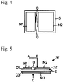
- Fig. 4 shows a ceramic circuit board having metal sheets M1, M2 laterally formed on a ceramic substrate S with a gap G. Brazing material portions protruding on the silicon nitride substrate S during the production of a bonded body of a silicon nitride substrate S and a copper sheet M are not completely removed by the copper-etching treatment, leaving residual brazing material portions protruding from ends of the circuit patterns (metal sheets M1, M2) in the gap G in which the copper sheet is removed by etching. They are called "brazing material protrusions D.”
- the brazing material protrusions D are composed of other metals than Cu in the brazing material. They presumably contain, for example, Ag (alloy) and TiN (reaction product). To remove these residues, a first brazing-material-etching treatment is conducted. A second brazing-material-etching treatment is further conducted.
- the bonded body is immersed in the first acidic solution comprising carboxylic acid and/or carboxylate and hydrogen peroxide (first brazing-material-etching solution), to etch the brazing material protrusions D.
- the first brazing-material-etching solution is preferably an aqueous solution comprising, for example, 0.083-1.7 mol/L of carboxylic acid and/or carboxylate, and 2.9-8.9 mol/L of hydrogen peroxide, and having pH of 2 to 4.
- the concentrations of carboxylic acid and/or carboxylate are expressed by their total.
- Carboxylic acid and/or carboxylate in the first brazing-material-etching solution may be only carboxylic acid or carboxylate or both.
- the counter salts are preferably Li + , Na + , K + , etc.
- the carboxylic acids and/or carboxylates are selected from the group consisting of formic acid, acetic acid, glycolic acid, and their salts, and from the aspect of cost and handling, acetic acid is most preferable.
- the concentration of carboxylic acid and/or carboxylate is preferably 0.1-1.5 mol/L, more preferably 0.2-1.4 mol/L, in total.
- the first brazing-material-etching solution has pH of 1 to 5. At pH of higher than 6, it exhibits lower capability of removing the brazing material.
- the pH is preferably 2-4.
- carboxylic acid is used, the aqueous solution is acidic, usually needing no pH adjustment.
- carboxylate is used, the pH of the aqueous solution is adjusted to 1 to 5 by acids described below, if necessary.
- the dissolving speed of a residual brazing material is determined by the decomposition reaction of hydrogen peroxide, and its dissolving capability depends on the concentration of carboxylic acid and/or carboxylate. For example, 3% by mass (0.5 mol/L) of acetic acid can dissolve 10 g/L of Ag. Because the decomposition reaction of hydrogen peroxide largely varies depending on the temperature, the temperature of a chain-reacting solution is stably kept preferably in a range from room temperature to lower than 50°C, further preferably in a range from room temperature to 40°C.
- hydrogen peroxide commercially available hydrogen peroxide water may be used.
- concentration of hydrogen peroxide is preferably 3-8 mol/L. It is preferable to use water from which impurities are removed by an ion exchange resin and/or a reverse osmosis membrane, which may be called “ion-exchanged water” or “deionized water.”
- the first brazing-material-etching solution may contain a defoaming agent, a surfactant, a pH-adjusting agent, a stabilizing agent, etc.
- the surfactant may be polyoxyethylenelauryl ether, polyoxyethylenestearyl ether, monoethanolamine, triethanolamine, etc.
- the defoaming agent may be polyoxyalkylenealkyl ether, polyoxyethylenealkylene ether, silicones, etc.
- the pH-adjusting agent may be alkalis such as sodium hydroxide, potassium hydroxide, ammonia water, etc.; and acids such as hydrochloric acid, sulfuric acid, nitric acid, phosphoric acid, etc.
- the stabilizing agent may be sulfuric acid, urea, phosphoric acid, etc.
- the first brazing-material-etching solution preferably contains 0.1-1.0% by mass of sulfuric acid, 1.0-5.0% by mass of urea, 10-100 ppm by mass of phosphoric acid, etc. They may be used in the second and third brazing-material-etching solutions described later.
- first brazing-material-etching solution may be exchanged to a new first brazing-material-etching solution, or supplemented with components for the first brazing-material-etching solution, to recover the brazing-material-capability.
- the etching solution is entirely exchanged, the old first brazing-material-etching solution is discarded from a first etching bath, which is then filled with a new first brazing-material-etching solution.
- Etching with an entirely exchanged solution without supplementing components is identified as "no supplement,” and etching while supplementing components to the solution is identified as "with supplement.” The latter is a method in which consumed components are supplemented.
- the total concentration of carboxylic acid and/or carboxylate is preferably about 0.2-1.4 mol/L to keep balance with the amount of hydrogen peroxide decomposed.
- a solution containing only carboxylic acid and/or carboxylate in water is used, a residual brazing material cannot be etched.
- the bonded body is immersed in an acidic solution comprising ammonium fluoride and hydrogen peroxide (second brazing-material-etching solution), to etch a residual brazing material remaining after the first brazing-material-etching treatment.
- the second brazing-material-etching solution is an aqueous solution comprising ammonium fluoride and hydrogen peroxide, preferably an aqueous solution comprising 0.7-2.1 mol/L of ammonium fluoride, and 2.9-8.9mol/L of hydrogen peroxide, and having pH of 5 or less.
- ammonium fluoride As ammonium fluoride, ammonium hydrogen fluoride [chemical formula: (NH 4 ) HF 2 ] as a hydrogen salt, or ammonium fluoride [chemical formula: NH 4 F] as a normal salt are usable.
- the former may be called acidic ammonium fluoride.
- ammonium fluoride as a normal salt should be properly handled to avoid the generation of HF and ammonia by decomposition, and sulfuric acid, etc. should be added to adjust pH (to avoid weak alkalization), thereby keeping the solution acidic. Accordingly, ammonium hydrogen fluoride is preferably used.
- the concentration of ammonium fluoride is preferably 1-2 mol/L, more preferably 1.2-1.8 mol/L.
- hydrogen peroxide commercially available hydrogen peroxide water may be used.
- concentration of hydrogen peroxide is preferably 3-8 mol/L.
- Water used is preferably water from which impurities are removed by an ion exchange resin and/or a reverse osmosis membrane, which is called ion-exchanged water or deionized water.
- the pH of the second brazing-material-etching solution is 5 or less. At pH of higher than 5, it has low capability of removing the brazing material.
- the pH is preferably 4.5 or less, more preferably 1-4.5, most preferably 2-4.
- the pH of the second brazing-material-etching solution is adjusted to 5 or less by acids or alkalis described later, if necessary.
- the temperature of the second brazing-material-etching solution is kept preferably in a range from room temperature to lower than 50°C, more preferably in a range from room temperature to 40°C.
- the second brazing-material-etching solution may contain a defoaming agent, a surfactant, a pH-adjusting agent, a stabilizing agent, etc.
- the defoaming agent, the surfactant, the pH-adjusting agent and the stabilizing agent may be the same compounds or agents as used in the first brazing-material-etching solution described above.
- the second brazing-material-etching solution preferably contains 0.1-1.0% by mass of sulfuric acid, 1.0-5.0% by mass of urea, 10-100 ppm by mass of phosphoric acid, etc.
- Cl - ions in the copper-etching solution may form a salt of silver chloride (AgCl) with Ag ions in the brazing material, and the silver chloride may hinder a subsequent first brazing-material-etching step.
- the bonded body may be immersed in a sodium thiosulfate solution to etch silver chloride, if necessary.
- the etching treatment with a sodium thiosulfate solution may be omitted.
- This etching treatment with sodium thiosulfate is conducted, for example, by immersing the bonded body in an aqueous solution containing 5-15% by mass of sodium thiosulfate for 10-30 minutes, with ultrasound applied.
- the temperature of the solution is preferably 10-30°C.
- silver chloride etched by sodium thiosulfate it is possible to prevent silver chloride from hindering the first brazing-material-etching step.
- the treatment with sodium thiosulfate etches only silver chloride, but does not etch Ag.
- the resist layers are removed, and a chemical polishing treatment, an anti-rust treatment, plating, etc. are further carried out to obtain a ceramic substrate having a copper circuit pattern.
- a chemical polishing treatment, an anti-rust treatment, plating, etc. are further carried out to obtain a ceramic substrate having a copper circuit pattern.
- an alkali-removable resist is used, the resist layers are removed with an alkaline solution (for example, an aqueous solution of 8-12% by mass of sodium hydroxide kept at about 50°C). Apart from sodium hydroxide, potassium hydroxide may be used.
- the treatment temperature may be in a range of 30-70°C.
- first and second brazing-material-etching solutions of the present invention are acidic aqueous solutions, these brazing-material-etching treatments do not remove the alkali-removable resist layers, thereby avoiding damage to the copper circuit pattern and the ceramic substrate.
- the chemical polishing is effective not only to remove surface oxides formed during the treatment, but also to adjust surface conditions. Namely, demands on gloss, matt, roughness, etc. can be met by selecting etching solutions and methods depending on electronic devices such as semiconductor chips mounted onto a copper circuit pattern, and metal wiring on the ceramic substrate.
- the circuit board W obtained by the above method has a basic structure comprising a ceramic substrate S, two brazing materials C1, C2 formed on an upper surface of the ceramic substrate S, two metal sheets M1, M2 bonded to the ceramic substrate S via two brazing materials C1, C2, and a gap G separating the brazing materials C1, C2 and the metal sheets M1, M2 in a planar direction.
- the metal sheets M1, M2 act as a circuit board, on which semiconductor devices, etc. are mounted.
- the circuit board W comprises a metal sheet M3 as a heat-dissipating plate bonded to a lower surface (rear surface) of the ceramic substrate S via a brazing material C3.
- a plating layer of Ni, Au, etc. may be formed on two metal sheets M1, M2, if necessary.
- the production method according to the second embodiment of the present invention is the same as in the first embodiment, except for carrying out the etching treatment of the bonded body with the third acidic solution (third brazing-material-etching solution) to remove the brazing material, in place of the first and second brazing-material-removing steps.
- the brazing material is removed with the third brazing-material-etching solution (third brazing-material-removing step), after the bonding step and the pattern-forming step are conducted in the same manner as in the first embodiment.
- etching with sodium thiosulfate, polishing and plating are conducted, if necessary. Because other steps than the brazing-material-removing step are the same as in the first embodiment, explanation will be made below on the third brazing-material-removing step carried out in place of the first and second brazing-material-removing steps.
- the third brazing-material-removing step in the second embodiment uses a third brazing-material-etching solution comprising components in the first and second brazing-material-etching solutions in the first embodiment in one bath.
- the third brazing-material-etching solution is the third acidic solution, for example, an aqueous solution comprising 0.083-1.7 mol/L of carboxylic acid and/or carboxylate, 0.7-2.1 mol/L of ammonium fluoride, and 2.9-8.9 mol/L of hydrogen peroxide, and having pH of 2 to 4.
- Carboxylic acid and/or carboxylate, ammonium fluoride and hydrogen peroxide used in the third brazing-material-etching solution are the same as used in the first and second brazing-material-etching solutions.
- the total concentration of carboxylic acid and/or carboxylate is preferably 0.1-1.5 mol/L, more preferably 0.2-1.4 mol/L.
- the concentration of ammonium fluoride is preferably 1-2 mol/L, more preferably 1.2-1.8 mol/L.
- the concentration of hydrogen peroxide is preferably 3-8 mol/L.
- the pH of the third brazing-material-etching solution is 1 to 5. At pH of higher than 6, it has low capability of removing the brazing material.
- the pH is preferably 2-4.
- carboxylic acid When carboxylic acid is used, pH adjustment is usually unnecessary because its aqueous solution is acidic.
- carboxylate is used, the pH is adjusted to 1 to 5 by acid, if necessary.
- Usable acids are the same as used in the first brazing-material-etching solution.
- the third brazing-material-etching solution may contain the same defoaming agent, surfactant, pH-adjusting agent, stabilizing agent, etc., as in the first and second brazing-material-etching solutions, if necessary.
- the defoaming agent, the surfactant, the pH-adjusting agent and the stabilizing agent may be the same compounds or agents as usable in the first and second brazing-material-etching solutions described above.
- the third brazing-material-etching solution preferably contains 0.1-1.0% by mass of sulfuric acid, 1.0-5.0% by mass of urea, 10-100 ppm by mass of phosphoric acid, etc.
- Treatment conditions, such as the temperature of the third brazing-material-etching solution, etc. may be the same as in the second brazing-material-removing step.
- the ceramic circuit board comprises a ceramic substrate, at least two brazing material layers formed on the ceramic substrate via a gap, and at least two metal sheets bonded to the ceramic substrate via at least two brazing material layers.
- Insulation resistance between two metal sheets is preferably 500 M ⁇ /mm or more.
- the numbers of the brazing material layers and the metal sheets bonded are not restricted to 2, but may be 3 or more. In this case, 3 or more metal sheets can be bonded. With insulation resistance of 500 M ⁇ /mm or more between two metal sheets, insulation between two metal sheets is not broken, thereby preventing excess current from passing through semiconductor devices, in a circuit board comprising semiconductor devices mounted on two metal sheets on a ceramic substrate.
- the ceramic circuit board is preferably produced by the above method of the present invention.
- the ceramic circuit board having such high insulation resistance as described above is obtained, for example, by removing brazing material portions remaining in a gap between two metal sheets on the ceramic substrate by the above brazing-material-removing treatment.
- the ceramic substrate used in the ceramic circuit board are not particularly restricted, but may be basically electrically insulating sintered materials.
- the ceramic substrate is preferably made of a nitride ceramic having high thermal conductivity.
- the ceramic substrate is preferably composed of sintered aluminum nitride comprising aluminum-nitride-based main phase particles and sintering-aid-based grain boundary phases existing between the particles, or a silicon-nitride-based sintered body comprising silicon-nitride-based main phase particles and sintering-aid-based grain boundary phases existing between the particles.
- the ceramic substrate S is more preferably composed of a silicon-nitride-based sintered body.
- the maximum diameter of pores on the ceramic substrate surface in the gap is preferably 2-15 ⁇ m.
- the maximum diameter of the pores is less than 2 ⁇ m, additives may not be fully removed by a washing agent.
- the ceramic substrate has low strength, so that the ceramic circuit board exhibits poor reliability, for example, in a cooling and heating cycle.
- the ceramic substrate composed of a silicon-nitride-based sintered body can be produced, for example, by mixing starting material powders comprising 90-97% by mass of silicon nitride and 0.5-10% by mass of a sintering aid, which may contain Mg or Y and other rare earth elements, with proper amounts of an organic binder, a plasticizer, a dispersant and an organic solvent by a ball mill, etc. to form a slurry, forming the slurry into a thin ceramic green sheet by a doctor blade method or a calendar rolling method, punching or cutting the green sheet to a desired shape, and sintering it at a temperature of 1700-1900°C.
- a sintering aid which may contain Mg or Y and other rare earth elements
- the sintering aid When the sintering aid is more than 10% by mass, the ceramic substrate is not sufficiently bonded to the ceramic circuit board. When the sintering aid is less than 0.5% by mass, silicon nitride particles are not fully sintered. The amount of the sintering aid is more preferably 3-10% by mass. To obtain high thermal conductivity and high strength, the sintering aid preferably comprises 2-4% by mass (as magnesium oxide) of magnesium (Mg), and 2-5% by mass (as yttrium oxide) of yttrium (Y).
- Materials for the metal sheet constituting the ceramic circuit board are not particularly restricted, as long as the metal sheet can be bonded by the brazing material, and has a higher melting point than that of the brazing material.
- copper, copper alloys, aluminum, aluminum alloys, silver, silver alloys, nickel, nickel alloys, nickel-plated molybdenum, nickel-plated tungsten, and nickel-plated iron alloys may be used for the metal sheet.
- copper or copper-containing alloys are most preferable, because of high electric resistance, ductility and thermal conductivity (low thermal resistance), low migration, etc.
- Aluminum or aluminum-containing alloys are preferable because of their plastic deformability which provides high mounting reliability in a cooling and heating cycle, despite lower electric resistance and thermal conductivity (higher thermal resistance) than those of copper.
- the brazing material layers C1-C3 bonding the metal sheets M1-M3 to the ceramic substrate S are preferably made of an active Ag-Cu brazing material, which is based on Ag and Cu having a eutectic composition for high strength, high sealability, etc., and contains active metals such as Ti, Zr, Hf, etc. Further, from the aspect of bonding strength between the ceramic substrate and the metal sheet, an active Ag-Cu-In brazing material containing In in an active Ag-Cu brazing material is more preferable. As described above, the metal sheet is bonded to the ceramic substrate S, using a brazing material paste comprising brazing material component powders in an organic binder.
- Brazing material layers c1, c2 comprising Ag and Cu as main components and further active metallic Ti were formed as shown in Fig. 1 by a screen-printing method, on both sides of a silicon nitride substrate S (area: 50 mm x 50 mm, and thickness: 150 ⁇ m).
- the silicon nitride substrate S was composed of silicon nitride particles and grain boundary phases containing a rare earth element.
- a paste was obtained by blending 100 parts by mass of alloy powders comprising 70% by mass of Ag, 3% by mass of In, and 27% by mass of Cu, with 0.3 parts by mass of TiH 2 , and an organic solvent, and the brazing material layers c1, c2 were formed by the paste.
- brazing material coated on the substrate was dried, 0.3-mm-thick copper sheets M were attached to the circuit pattern side (front side) and the heat dissipation pattern side (rear side), and heat-treated at 750-850°C for 20 minutes in vacuum while being compressed, to form a bonded body of the silicon nitride substrate S and the copper sheets M.
- Brazing material layers C1, C2 as thick as about 30 ⁇ m were formed between the silicon nitride substrate S and the copper sheets M.
- the copper sheet M of each bonded body was coated with an ultraviolet-curable etching resist ink, and then irradiated with ultraviolet rays to cure the etching resist ink, thereby forming resist layer patterns R1, R2.
- This etching resist ink was removable with alkali.
- a first brazing-material-etching treatment etching with an acidic solution comprising carboxylic acid and/or carboxylate and hydrogen peroxide
- a second brazing-material-etching treatment etching with a solution containing ammonium hydrogen fluoride and hydrogen peroxide
- the brazing material protrusions D presumably had a composition comprising a main phase of Ag and a TiN phase.
- etching with an acidic solution comprising carboxylic acid and/or carboxylate and hydrogen peroxide was conducted as the first brazing-material-etching step.
- the bonded body having brazing material protrusions D was immersed in an aqueous solution containing 3% by mass (0.5 mol/L) of acetic acid and 20% by mass (5.9 mol/L) of hydrogen peroxide and having pH of 3 (first brazing-material-etching solution), at 30°C for 20 minutes. Ion-exchanged water was used in the first brazing-material-etching solution.
- the brazing material protrusions D having metallic gloss after forming patterns lost metallic gloss by the first brazing-material-etching treatment, resulting in clear contrast between the silicon nitride substrate S and the brazing material protrusions D.
- the bonded body after the first brazing-material-etching treatment was immersed in an aqueous solution containing 4% by mass (0.7 mol/L) of ammonium hydrogen fluoride, 26% by mass (7.6 mol/L) of hydrogen peroxide, 1% by mass (0.2 N) of sulfuric acid, 3% by mass (0.5 mol/L) of urea, and 100 ppm (1.0 mmol/L) of phosphoric acid, and having pH of 3 (second brazing-material-etching solution), at 40°C for 20 minutes. Ion-exchanged water was used in the second brazing-material-etching solution. The brazing material protrusions were substantially removed by the second brazing-material-etching treatment.
- the bonded bodies were treated with an aqueous solution of 3% by mass of sodium hydroxide to remove the resist layers.
- circuit patterns on the front side and a copper sheet on the rear side were plated with Ni.
- the chemical polishing for gloss was conducted with a commercially available sulfuric-acid-based solution.
- a ceramic circuit board silicon nitride circuit board shown in Fig. 5 was obtained.
- Ceramic circuit boards were produced in the same manner as in Example 1, except for changing the treatment temperature and time in the first and second brazing-material-etching treatments as shown in Table 1.
- a ceramic circuit board was produced in the same manner as in Example 2, except that the first brazing-material-etching treatment was not conducted.
- Comparative Example 1 only the second brazing-material-etching step using ammonium hydrogen fluoride and hydrogen peroxide was conducted, without the first brazing-material-etching step using acetic acid and hydrogen peroxide. Accordingly, the brazing material was not fully removed, resulting in a pass rate of 60% or less. Thus, another step of discarding poor products is needed in the method of Comparative Example 1.
- Ceramic circuit boards were produced in the same manner as in Example 1, except that each bonded body having brazing material protrusions D was immersed in an aqueous solution comprising 3% by mass (0.5 mol/L) of acetic acid, 4% by mass (0.7 mol/L) of ammonium hydrogen fluoride, 26% by mass (7.6 mol/L) of hydrogen peroxide, 1% by mass (0.2 N) of sulfuric acid, 3% by mass (0.5 mol/L) of urea, and 100 ppm (1.0 mmol/L) of phosphoric acid, and having pH of 3 (third brazing-material-etching solution), at 40°C for 30 minutes, instead of conducting the first and second brazing-material-etching treatments.
- the ceramic circuit boards were produced at as high a pass rate as 100% (evaluated as Good). Because the third brazing-material-etching solution was not alkaline, resist layers were not dissolved, thereby causing no damages on the circuit patterns.
- Ceramic circuit boards were produced in the same manner as in Example 1, except for using, as a brazing material, a paste obtained by blending 100 parts by mass of alloy powders comprising 65.5% by mass of Ag and 2% by mass of In, the balance being Cu, with 15 parts by mass of Ag and 0.2 parts by mass of TiH 2 , and further with an organic solvent.
- the ceramic circuit boards were produced at a pass rate of 100% (evaluated as Good).
- Ceramic circuit boards were produced in the same manner as in Example 1, except for using, as a brazing material, a paste obtained by blending 100 parts by mass of alloy powders comprising 50% by mass of Ag, 25% by mass of In, and 25% by mass of Cu, with 0.2 parts by mass of Ti and an organic solvent.
- the ceramic circuit boards were produced at a pass rate of 100% (evaluated as Good).
- Ceramic circuit boards were produced in the same manner as in Example 1, except for changing the amounts of acetic acid and hydrogen peroxide in the first brazing-material-etching solution, and the first brazing-material-etching treatment time as shown in Table 2.
- the ceramic circuit boards were produced at as high pass rates as shown in Table 2.
- Example 14 used 0.8% by mass (0.13 mol/L) of acetic acid, and 26% by mass (7.6 mol/L) of hydrogen peroxide;
- Example 15 used 1.7% by mass (0.28 mol/L) of acetic acid, and 23% by mass (6.8 mol/L) of hydrogen peroxide;
- Example 16 used 2.8% by mass (0.47 mol/L) of acetic acid, and 17% by mass (5.0 mol/L) of hydrogen peroxide;
- Example 17 used 3.0% by mass (0.5 mol/L) of acetic acid, and 24% by mass (7.1 mol/L) of hydrogen peroxide; and
- Example 18 used 5.1% by mass (0.85 mol/L) of acetic acid, and 10% by mass (2.9 mol/L) of hydrogen peroxide.
- Ceramic circuit boards were produced in the same manner as in Example 1, except for changing the concentrations of ammonium hydrogen fluoride and hydrogen peroxide in the second brazing-material-etching solution, and the second brazing-material-etching treatment time as shown in Table 3.
- the ceramic circuit boards were produced at as high pass rates as shown in Table 3.
- Example 19 used 15% by mass (4.4 mol/L) of hydrogen peroxide, and 3.4% by mass (0.60 mol/L) of ammonium hydrogen fluoride;
- Example 20 used 25% by mass (7.4 mol/L) of hydrogen peroxide, and 8.1% by mass (1.4 mol/L) of ammonium hydrogen fluoride; and
- Example 21 used 30% by mass (8.8 mol/L) of hydrogen peroxide, and 15% by mass (2.6 mol/L) of ammonium hydrogen fluoride.
- Example 19 40 15 3.4 Good
- Example 20 25 8.1 Good
- Example 21 20 30 15 Good
- Ceramic circuit boards were produced in the same manner as in Example 11, except for changing the concentrations of acetic acid, ammonium hydrogen fluoride and hydrogen peroxide in the third brazing-material-etching solution, and the third brazing-material-etching treatment time as shown in Table 4.
- the ceramic circuit boards were produced at as high pass rates as shown in Table 4.
- Example 22 used 1.1% by mass (0.18 mol/L) of acetic acid, 20% by mass (5.9 mol/L) of hydrogen peroxide, and 8% by mass (1.4 mol/L) of ammonium hydrogen fluoride;
- Example 23 used 1.7% by mass (0.28 mol/L) of acetic acid, 23% by mass (6.8 mol/L) of hydrogen peroxide, and 4% by mass (0.70 mol/L) of ammonium hydrogen fluoride;
- Example 24 used 2.8% by mass (0.47 mol/L) of acetic acid, 18% by mass (5.3 mol/L) of hydrogen peroxide, and 10.5% by mass (1.8 mol/L) of ammonium hydrogen fluoride; and
- Example 25 used 12% by mass (2.0 mol/L) of acetic acid, 8% by mass (2.4 mol/L) of hydrogen peroxide, and 8% by mass (1.4 mol/L) of ammonium hydrogen fluoride.
- Ceramic circuit boards were produced in the same manner as in Example 1, except that after the pattern-forming step and before the first brazing-material-etching step, the bonded bodies were immersed in an aqueous solution of 10% by mass of sodium thiosulfate at 20°C for 20 minutes for etching. The etching treatment was conducted while applying ultrasound of 600 W and 35 kHz to the aqueous sodium thiosulfate solution. Ion-exchanged water was used in the sodium thiosulfate aqueous solution. As in Example 1, the ceramic circuit boards were produced at a high pass rate (evaluated as Good).
- Ceramic circuit boards were produced in the same manner as in Example 1, except that an aqueous solution obtained by dropping 3-N hydrochloric acid into an aqueous solution (about pH 6) comprising 2.3% by mass (0.34 mol/L) of sodium formate and 10% by mass (2.9 mol/L) of hydrogen peroxide to adjust the pH to 3 was used as the first brazing-material-etching solution, and that the bonded bodies were immersed in the above aqueous solution at 40°C for 30 minutes for etching. The pass rate was as high as 90% or more (evaluated as Good).
- Ceramic circuit boards were produced in the same manner as in Example 1, except that an aqueous solution comprising 3.8% by mass (0.5 mol/L) of glycolic acid and 15% by mass (4.4 mol/L) of hydrogen peroxide, and having pH of about 3 was used as the first brazing-material-etching solution, and that the bonded bodies were immersed in the above aqueous solution at 40°C for 30 minutes for etching.
- the pass rate was as high as 90% or more (evaluated as Good).
- the ceramic circuit boards produced in Examples 1-10 and Comparative Example 1 were subjected to an insulation breakdown voltage test, which measured insulation breakdown voltage when AC voltage was applied between front and rear surfaces of each ceramic circuit board. As shown in Fig. 5 , with electrodes A and B attached to the metal sheets M1 and M2 for short-circuiting between A and B, and an electrode C (not shown) attached to the metal sheet M3 on a rear surface of the ceramic circuit board, this ceramic circuit board was immersed in an insulating silicone oil at room temperature.
- AC voltage having a frequency of 50 Hz which was applied between the front and rear surfaces of each ceramic circuit board (between the heat-dissipating plate and the circuit plates) by a breakdown voltage tester TOS5101 available from Kikusui Electronics Corp., was gradually increased from 0 kV to 10 kV at a speed of 0.1 kV/sec, and voltage at which insulation was broken by drastically increased leak current was regarded as insulation breakdown voltage. This measurement was carried out on 20 samples of each ceramic circuit board, and the measured values were averaged.
- the passed products having brazing material protrusions of 0.2 mm or less exhibited insulation breakdown voltage of 5 kV or more, indicating that they had sufficient insulation.
- the failed products having brazing material protrusions of more than 0.2 mm around the copper sheets exhibited insulation breakdown voltage of less than 5 kV.
- the ceramic circuit boards produced in Examples 1-10 and Comparative Example 1 were measured with respect to insulation resistance between metal sheets. As shown in Fig. 5 , DC voltage of 1000 V was applied between spherical electrodes A, B connected to arbitrary portions of the metal (copper) sheets M1 and M2, to measure resistance after 30 seconds as insulation resistance. The distance between the metal sheets M1 and M2 was 1 mm. The minimum insulation resistance measured on 10 ceramic circuit boards of each Example and Comparative Example was used for evaluation. The insulation resistance was 500 M ⁇ /mm or more between terminals in the passed products having brazing material protrusions of 0.2 mm or less, while it was less than 500 M ⁇ /mm between terminals in the failed products having brazing material protrusions of more than 0.2 mm.
- the method of the present invention is suitable for producing small or high-power ceramic circuit boards.
- the brazing-material-removing step uses an etching solution comprising carboxylic acid and/or carboxylate, and hydrogen peroxide in the method of the present invention for producing a ceramic circuit board
- brazing materials are highly efficiently removed, without eroding an alkali-removable etching resist because the etching solution is acidic. Accordingly, ceramic circuit boards can be produced at high pass rates. Because inexpensive and easy-to-handle carboxylic acid or its salt is used, the method is highly safe with large cost advantages.
Landscapes
- Engineering & Computer Science (AREA)
- Chemical & Material Sciences (AREA)
- Ceramic Engineering (AREA)
- Microelectronics & Electronic Packaging (AREA)
- Manufacturing & Machinery (AREA)
- Materials Engineering (AREA)
- Organic Chemistry (AREA)
- Condensed Matter Physics & Semiconductors (AREA)
- Computer Hardware Design (AREA)
- Power Engineering (AREA)
- General Physics & Mathematics (AREA)
- Structural Engineering (AREA)
- Physics & Mathematics (AREA)
- Inorganic Chemistry (AREA)
- Chemical Kinetics & Catalysis (AREA)
- General Chemical & Material Sciences (AREA)
- Mechanical Engineering (AREA)
- Metallurgy (AREA)
- Manufacturing Of Printed Circuit Boards (AREA)
- Powder Metallurgy (AREA)
- Manufacturing Of Printed Wiring (AREA)
Description
- The present invention relates to a method for producing a ceramic circuit board used for power modules, etc.
- To be used for power modules in electric vehicles (EV), etc., ceramic circuit boards comprising copper sheets bonded to ceramic substrates having good thermal conductivity via brazing materials have become increasingly demanded. Such circuit boards are generally produced by coating substrates of ceramics such as silicon nitride, aluminum nitride, etc. having high thermal conductivity with a brazing material containing an active metal; heat-bonding a metal sheet of copper, aluminum, etc. to the brazing material; printing a resist in a circuit pattern on the metal sheet; and removing unnecessary metal sheet portions covered with no resist by etching.
- When a copper sheet is bonded to a sintered silicon nitride substrate with a brazing material comprising Ag, Cu, and Ti (active metal) as described in Japanese Patent
3,629,783 - Unnecessary brazing material portions between circuit patterns are removed to some extent when the metal sheet is etched, but an alloy layer (for example, mainly composed of Cu-Ag) and a reaction product layer (for example, mainly composed of titanium nitride) in the brazing material may partially remain without being completely removed as the case may be. A partially remaining brazing material decreases insulation or causing short-circuiting between adjacent circuit patterns.
-
JP 2006-351988 A JP 2006-351988 A -
JP 9-162325 A JP 9-162325 A JP 9-162325 A - To remove unnecessary brazing material portions between circuit patterns completely, it is known that after the copper sheet is etched, the brazing material is further etched. For example,
JP 10-154866 A JP 10-154866 A JP 10-154866 A -
JP 10-251878 A JP 10-251878 A JP 10-251878 A -
JP 2005-35874 A JP 2005-35874 A - However, the production method of a metal-bonded ceramic substrate described in
JP 2005-35874 A - Document
US 2003/0066865 A1 discloses a method for producing a metal/ceramic bonding circuit board. Two copper plates are bonded to both sides of a ceramic substrate via brazing filler metal. Subsequently UV curing alkali peeling type resists are applied in predetermined portions on the surfaces of the copper plates to etch undesired portions of the copper plates and form a metal circuit portion. While the resists are maintained, undesired portions of the brazing filler metal and a reaction product, which is produced by a reaction of the brazing filler metal with the ceramic substrate, are removed. Thereafter, the resists are peeled off, and a Ni-P electroless plating is carried out. - Accordingly, an object of the present invention is to provide a method for producing a ceramic circuit board by using a treating solution having high brazing-material-removing capability and good handleability, which does not corrode an etching resist to be removed by an alkaline solution.
- As a result of intensive research in view of the above object, the inventor has found that an acidic solution comprising carboxylic acid and/or carboxylate and hydrogen peroxide has high capability of removing a brazing material containing Ag, and very good handleability, and that by a subsequent treatment with an acidic solution comprising ammonium fluoride and hydrogen peroxide, a trace amount of a residual brazing material can be removed to a practically acceptable level. The present invention has been completed based on such finding.
- A usual production method of a ceramic circuit board comprises bonding a metal sheet to a ceramic substrate via a brazing material to form a bonded body, etching the bonded metal sheet to form a circuit pattern, and then further etching the circuit pattern. Etching with a conventional etching solution (for example, an aqueous solution comprising ammonium fluoride and hydrogen peroxide as described in
JP 10-154866 A - Thus, the method of the present invention for producing a ceramic circuit board is as defined in claim 1.
- The brazing material preferably contains Ag and an active metal.
- The second acidic solution comprising ammonium fluoride and hydrogen peroxide is preferably an aqueous solution comprising 0.7-2.1 mol/L of ammonium fluoride and 2.9-8.9 mol/L of hydrogen peroxide, and having pH of 5 or less.
- The second acidic solution comprising ammonium fluoride and hydrogen peroxide preferably further comprises at least one of sulfuric acid, urea, and phosphoric acid.
- The first acidic solution comprising carboxylic acid and/or carboxylate and hydrogen peroxide is preferably an aqueous solution comprising 0.083-1.7 mol/L of carboxylic acid and/or carboxylate and 2.9-8.9 mol/L of hydrogen peroxide, and having pH of 2 to 4.
- The first acidic solution comprising carboxylic acid and/or carboxylate and hydrogen peroxide preferably further comprises at least one of sulfuric acid, urea, and phosphoric acid.
- The third acidic solution comprising carboxylic acid and/or carboxylate, ammonium fluoride, and hydrogen peroxide is preferably an aqueous solution comprising 0.083-1.7 mol/L of carboxylic acid and/or carboxylate, 0.7-2.1 mol/L of ammonium fluoride, and 2.9-8.9 mol/L of hydrogen peroxide, and having pH of 2 to 4.
- The third acidic solution comprising carboxylic acid and/or carboxylate, ammonium fluoride, and hydrogen peroxide preferably further comprises at least one of sulfuric acid, urea, and phosphoric acid.
- It is preferable that the metal sheet is a copper sheet, and that a solution for etching the bonded metal sheet in the pattern-forming step is preferably a copper-etching solution.
- The brazing material preferably contains Ag, Cu, and an active metal.
-
-
Fig. 1 is a plan view schematically showing a brazing material screen-printed onto a ceramic substrate. -
Fig. 2 is a plan view schematically showing a bonded body comprising a metal sheet bonded to a ceramic substrate via a brazing material. -
Fig. 3 is a plan view schematically showing a bonded body having a metal sheet, which is coated with a resist for forming desired circuit patterns. -
Fig. 4 is a plan view schematically showing residual brazing material portions after an unnecessary metal sheet portion is removed by etching. -
Fig. 5 is a front view showing a ceramic circuit board. - The method for producing a ceramic circuit board according to the first embodiment of the present invention will be explained below. This method comprises
bonding a metal sheet to a ceramic substrate via a brazing material containing Ag to form a bonded body;
etching the bonded metal sheet to form a circuit pattern; and
removing an unnecessary brazing material from the substrate provided with the circuit pattern, by etching with the first acidic solution, and then removing a residual brazing from said substrate having an unnecessary brazing material removed, by etching with the second acidic solution. - As shown in
Fig. 1 , a surface of a ceramic substrate S (silicon nitride substrate, aluminum nitride substrate, etc.) are screen-printed with brazing materials C1, C2 containing an active metal to form patterns separate from each other via a gap G. A metal sheet M (copper sheet, aluminum sheet, etc.) is bonded under pressure to the ceramic substrate coated with the active-metal-containing brazing materials, and heated to the melting point of the active-metal-containing brazing material or higher in vacuum, or in an inert atmosphere such as an argon gas, etc., thereby forming a bonded body, in which the metal sheet M is integrally bonded to the ceramic substrate S via the brazing materials C1, C2 (seeFig. 2 ). The active-metal-containing brazing materials coated are preferably as thick as about 20-50 µm, to relax thermal expansion difference between the ceramic substrate and the metal sheet. The metal sheet M of the bonded body is provided with resist layers R1, R2 to form desired circuit patterns (seeFig. 3 ). - Likewise, a metal sheet M3 for a heat-dissipating plate is bonded to another surface of the ceramic substrate S with a brazing material C3 containing an active metal. In the production of a ceramic circuit board, because metal sheets M1, M2 for a circuit board, and a metal sheet M3 for a heat-dissipating plate are bonded basically in the same way, explanation will be made only on the metal sheets M1, M2, with the explanation of the metal sheet M3 omitted.
- A brazing material used in the present invention contains at least Ag and an active metal. As other metals than Ag and the active metal, Cu is preferably contained, and In may be further contained. Inevitable impurities may be contained. The brazing material is preferably composed of Ag, Cu, and an active metal. The active metal is, for example, at least one of Ti, Zr and Hf.
- The preferred brazing material powder is composed of alloy powder comprising 55-81% by mass of Ag, 1-5% by mass of In, 14-44% by mass of Cu, and inevitable impurities, Ag powder, and active metal hydride powder. In the alloy powder, a ratio of Ag/(Ag + Cu) is preferably 0.57-0.85. In the brazing material, the oxygen content is preferably 0.1% or less by mass, and the Si content is preferably 0.0001-0.5% by mass. The active metal hydride powder is preferably 1-3 parts by mass per 100 parts by mass of the alloy powder. The active metal hydride may be hydride of at least one metal selected from the group consisting of Ti, Zr and Hf, and is preferably Ti hydride.
- The brazing material may be a paste suitable for screen-printing, which is obtained by blending 100% by mass of the metal components (the total of an active metal and other metals) with 1-10% by mass of a binder, and 2-20% by mass of an organic solvent.
- The resist layers are preferably formed by an ultraviolet-curing resist. The ultraviolet-curing resist comprises a copolymer-type acrylate oligomer, an acrylate monomer, a filler, a photopolymerization initiator, a color-adjusting agent, a defoamer, and a leveling agent. The copolymer-type acrylate oligomer, a main component in the ultraviolet-curing resist, is a high-viscosity polymer which is cured by a polycondensation reaction. The copolymer-type acrylate oligomer as a main component may be epoxy acrylate, urethane acrylate, polyester acrylate, polyether acrylate, and other copolymers. Acrylate monomers include isoamyl acrylate, lauryl acrylate, stearyl acrylate, ethoxydiethylene glycol acrylate, 2-hydroxyethylacrylate, phenoxyethylacrylate, etc.
- Selecting a copper sheet as a metal sheet M, explanation will be made below. A bonded body having resist layers R1, R2 for forming circuit patterns is immersed in a copper-etching solution comprising copper chloride (CuCl2), hydrochloric acid (HCl) and hydrogen peroxide (H2O2), to etch copper sheet portions covered with no resist, for example, at 50°C. As the copper-etching solution, for example, a solution containing iron chloride may be used. Instead of immersing, the bonded body may be showered with the copper-etching solution. Copper sheet portions covered with no resist (unnecessary portions) are removed by this treatment, and part of the brazing material is then removed. In this example, Cu in the brazing material is mostly removed because the copper-etching solution is used, leaving residual brazing material portions containing Ag.
-
Fig. 4 shows a ceramic circuit board having metal sheets M1, M2 laterally formed on a ceramic substrate S with a gap G. Brazing material portions protruding on the silicon nitride substrate S during the production of a bonded body of a silicon nitride substrate S and a copper sheet M are not completely removed by the copper-etching treatment, leaving residual brazing material portions protruding from ends of the circuit patterns (metal sheets M1, M2) in the gap G in which the copper sheet is removed by etching. They are called "brazing material protrusions D." - Because Cu in the brazing material is mostly etched by the copper-etching treatment for forming patterns, the brazing material protrusions D are composed of other metals than Cu in the brazing material. They presumably contain, for example, Ag (alloy) and TiN (reaction product). To remove these residues, a first brazing-material-etching treatment is conducted. A second brazing-material-etching treatment is further conducted.
- The bonded body is immersed in the first acidic solution comprising carboxylic acid and/or carboxylate and hydrogen peroxide (first brazing-material-etching solution), to etch the brazing material protrusions D. The first brazing-material-etching solution is preferably an aqueous solution comprising, for example, 0.083-1.7 mol/L of carboxylic acid and/or carboxylate, and 2.9-8.9 mol/L of hydrogen peroxide, and having pH of 2 to 4. The concentrations of carboxylic acid and/or carboxylate are expressed by their total. Carboxylic acid and/or carboxylate in the first brazing-material-etching solution may be only carboxylic acid or carboxylate or both.
- Though not restrictive, the counter salts are preferably Li+, Na+, K+, etc. The carboxylic acids and/or carboxylates are selected from the group consisting of formic acid, acetic acid, glycolic acid, and their salts, and from the aspect of cost and handling, acetic acid is most preferable. The concentration of carboxylic acid and/or carboxylate is preferably 0.1-1.5 mol/L, more preferably 0.2-1.4 mol/L, in total.
- The first brazing-material-etching solution has pH of 1 to 5. At pH of higher than 6, it exhibits lower capability of removing the brazing material. The pH is preferably 2-4. When carboxylic acid is used, the aqueous solution is acidic, usually needing no pH adjustment. When carboxylate is used, the pH of the aqueous solution is adjusted to 1 to 5 by acids described below, if necessary.
- In the first brazing-material-etching treatment, the dissolving speed of a residual brazing material is determined by the decomposition reaction of hydrogen peroxide, and its dissolving capability depends on the concentration of carboxylic acid and/or carboxylate. For example, 3% by mass (0.5 mol/L) of acetic acid can dissolve 10 g/L of Ag. Because the decomposition reaction of hydrogen peroxide largely varies depending on the temperature, the temperature of a chain-reacting solution is stably kept preferably in a range from room temperature to lower than 50°C, further preferably in a range from room temperature to 40°C.
- As hydrogen peroxide, commercially available hydrogen peroxide water may be used. The concentration of hydrogen peroxide is preferably 3-8 mol/L. It is preferable to use water from which impurities are removed by an ion exchange resin and/or a reverse osmosis membrane, which may be called "ion-exchanged water" or "deionized water."
- The first brazing-material-etching solution may contain a defoaming agent, a surfactant, a pH-adjusting agent, a stabilizing agent, etc. The surfactant may be polyoxyethylenelauryl ether, polyoxyethylenestearyl ether, monoethanolamine, triethanolamine, etc. The defoaming agent may be polyoxyalkylenealkyl ether, polyoxyethylenealkylene ether, silicones, etc. The pH-adjusting agent may be alkalis such as sodium hydroxide, potassium hydroxide, ammonia water, etc.; and acids such as hydrochloric acid, sulfuric acid, nitric acid, phosphoric acid, etc. The stabilizing agent may be sulfuric acid, urea, phosphoric acid, etc. For example, the first brazing-material-etching solution preferably contains 0.1-1.0% by mass of sulfuric acid, 1.0-5.0% by mass of urea, 10-100 ppm by mass of phosphoric acid, etc. They may be used in the second and third brazing-material-etching solutions described later.
- As the etching continues, components are gradually consumed in the first brazing-material-etching solution, resulting in the decreased capability of removing the brazing material. The deteriorated first brazing-material-etching solution may be exchanged to a new first brazing-material-etching solution, or supplemented with components for the first brazing-material-etching solution, to recover the brazing-material-capability. When the etching solution is entirely exchanged, the old first brazing-material-etching solution is discarded from a first etching bath, which is then filled with a new first brazing-material-etching solution. Etching with an entirely exchanged solution without supplementing components is identified as "no supplement," and etching while supplementing components to the solution is identified as "with supplement." The latter is a method in which consumed components are supplemented.
- When the brazing material is etched by immersing samples in the solution without supplementing components, the total concentration of carboxylic acid and/or carboxylate is preferably about 0.2-1.4 mol/L to keep balance with the amount of hydrogen peroxide decomposed. When a solution containing only carboxylic acid and/or carboxylate in water is used, a residual brazing material cannot be etched.
- Because hydrogen peroxide is gradually decomposed in the first brazing-material-etching solution as the etching treatment of immersed samples proceeds, hydrogen peroxide is supplemented to the solution step by step, to always keep hydrogen peroxide in a proper concentration range. With carboxylic acid and/or carboxylate adjusted at high concentrations (for example, about 2.5 mol/L) in advance, exchange may be conducted when the concentration of carboxylic acid and/or carboxylate decreases to a certain level (for example, 0.33 mol/L or less) by supplementing hydrogen peroxide. This method enjoys a reduced frequency of exchanging solutions, effective for mass treatment. Namely, a life of the first brazing-material-etching solution in the first etching bath can be expanded, contributing to cost reduction. When the first brazing-material-etching solution is showered instead of immersing, higher concentrations of carboxylic acid and/or carboxylate are effective for sufficient dissolving capability, because the step-by-step measurement of the concentration of hydrogen peroxide is generally difficult. Because carboxylic acid and/or carboxylate may corrode stainless steel forming the apparatus and drainage facilities, their concentrations may be set as low as providing substantially no adverse effect on stainless steel.
- After the first brazing-material-etching treatment, the bonded body is immersed in an acidic solution comprising ammonium fluoride and hydrogen peroxide (second brazing-material-etching solution), to etch a residual brazing material remaining after the first brazing-material-etching treatment. The second brazing-material-etching solution is an aqueous solution comprising ammonium fluoride and hydrogen peroxide, preferably an aqueous solution comprising 0.7-2.1 mol/L of ammonium fluoride, and 2.9-8.9mol/L of hydrogen peroxide, and having pH of 5 or less.
- As ammonium fluoride, ammonium hydrogen fluoride [chemical formula: (NH4) HF2] as a hydrogen salt, or ammonium fluoride [chemical formula: NH4F] as a normal salt are usable. The former may be called acidic ammonium fluoride. When the latter is used, ammonium fluoride as a normal salt should be properly handled to avoid the generation of HF and ammonia by decomposition, and sulfuric acid, etc. should be added to adjust pH (to avoid weak alkalization), thereby keeping the solution acidic. Accordingly, ammonium hydrogen fluoride is preferably used. The concentration of ammonium fluoride is preferably 1-2 mol/L, more preferably 1.2-1.8 mol/L.
- As hydrogen peroxide, commercially available hydrogen peroxide water may be used. The concentration of hydrogen peroxide is preferably 3-8 mol/L. Water used is preferably water from which impurities are removed by an ion exchange resin and/or a reverse osmosis membrane, which is called ion-exchanged water or deionized water.
- The pH of the second brazing-material-etching solution is 5 or less. At pH of higher than 5, it has low capability of removing the brazing material. the pH is preferably 4.5 or less, more preferably 1-4.5, most preferably 2-4. The pH of the second brazing-material-etching solution is adjusted to 5 or less by acids or alkalis described later, if necessary. The temperature of the second brazing-material-etching solution is kept preferably in a range from room temperature to lower than 50°C, more preferably in a range from room temperature to 40°C.
- The second brazing-material-etching solution may contain a defoaming agent, a surfactant, a pH-adjusting agent, a stabilizing agent, etc. The defoaming agent, the surfactant, the pH-adjusting agent and the stabilizing agent may be the same compounds or agents as used in the first brazing-material-etching solution described above. For example, the second brazing-material-etching solution preferably contains 0.1-1.0% by mass of sulfuric acid, 1.0-5.0% by mass of urea, 10-100 ppm by mass of phosphoric acid, etc.
- In the pattern-forming step using a copper-etching solution, Cl- ions in the copper-etching solution may form a salt of silver chloride (AgCl) with Ag ions in the brazing material, and the silver chloride may hinder a subsequent first brazing-material-etching step. To avoid such trouble, after the copper-etching treatment and before the first brazing-material-etching step, the bonded body may be immersed in a sodium thiosulfate solution to etch silver chloride, if necessary. When silver chloride is formed little in the pattern-forming step, the etching treatment with a sodium thiosulfate solution may be omitted. This etching treatment with sodium thiosulfate is conducted, for example, by immersing the bonded body in an aqueous solution containing 5-15% by mass of sodium thiosulfate for 10-30 minutes, with ultrasound applied. The temperature of the solution is preferably 10-30°C. With silver chloride etched by sodium thiosulfate, it is possible to prevent silver chloride from hindering the first brazing-material-etching step. The treatment with sodium thiosulfate etches only silver chloride, but does not etch Ag.
- After the second brazing-material-etching step, the resist layers are removed, and a chemical polishing treatment, an anti-rust treatment, plating, etc. are further carried out to obtain a ceramic substrate having a copper circuit pattern. When an alkali-removable resist is used, the resist layers are removed with an alkaline solution (for example, an aqueous solution of 8-12% by mass of sodium hydroxide kept at about 50°C). Apart from sodium hydroxide, potassium hydroxide may be used. The treatment temperature may be in a range of 30-70°C. Because the first and second brazing-material-etching solutions of the present invention are acidic aqueous solutions, these brazing-material-etching treatments do not remove the alkali-removable resist layers, thereby avoiding damage to the copper circuit pattern and the ceramic substrate.
- The chemical polishing is effective not only to remove surface oxides formed during the treatment, but also to adjust surface conditions. Namely, demands on gloss, matt, roughness, etc. can be met by selecting etching solutions and methods depending on electronic devices such as semiconductor chips mounted onto a copper circuit pattern, and metal wiring on the ceramic substrate.
- As shown in
Fig. 5 , the circuit board W obtained by the above method has a basic structure comprising a ceramic substrate S, two brazing materials C1, C2 formed on an upper surface of the ceramic substrate S, two metal sheets M1, M2 bonded to the ceramic substrate S via two brazing materials C1, C2, and a gap G separating the brazing materials C1, C2 and the metal sheets M1, M2 in a planar direction. The metal sheets M1, M2 act as a circuit board, on which semiconductor devices, etc. are mounted. Further, the circuit board W comprises a metal sheet M3 as a heat-dissipating plate bonded to a lower surface (rear surface) of the ceramic substrate S via a brazing material C3. A plating layer of Ni, Au, etc. may be formed on two metal sheets M1, M2, if necessary. - The production method according to the second embodiment of the present invention is the same as in the first embodiment, except for carrying out the etching treatment of the bonded body with the third acidic solution (third brazing-material-etching solution) to remove the brazing material, in place of the first and second brazing-material-removing steps. Namely, in the second embodiment, the brazing material is removed with the third brazing-material-etching solution (third brazing-material-removing step), after the bonding step and the pattern-forming step are conducted in the same manner as in the first embodiment. As in the embodiment 1, etching with sodium thiosulfate, polishing and plating are conducted, if necessary. Because other steps than the brazing-material-removing step are the same as in the first embodiment, explanation will be made below on the third brazing-material-removing step carried out in place of the first and second brazing-material-removing steps.
- The third brazing-material-removing step in the second embodiment uses a third brazing-material-etching solution comprising components in the first and second brazing-material-etching solutions in the first embodiment in one bath. The third brazing-material-etching solution is the third acidic solution, for example, an aqueous solution comprising 0.083-1.7 mol/L of carboxylic acid and/or carboxylate, 0.7-2.1 mol/L of ammonium fluoride, and 2.9-8.9 mol/L of hydrogen peroxide, and having pH of 2 to 4. Carboxylic acid and/or carboxylate, ammonium fluoride and hydrogen peroxide used in the third brazing-material-etching solution are the same as used in the first and second brazing-material-etching solutions.
- The total concentration of carboxylic acid and/or carboxylate is preferably 0.1-1.5 mol/L, more preferably 0.2-1.4 mol/L. The concentration of ammonium fluoride is preferably 1-2 mol/L, more preferably 1.2-1.8 mol/L. The concentration of hydrogen peroxide is preferably 3-8 mol/L.
- The pH of the third brazing-material-etching solution is 1 to 5. At pH of higher than 6, it has low capability of removing the brazing material. The pH is preferably 2-4. When carboxylic acid is used, pH adjustment is usually unnecessary because its aqueous solution is acidic. When carboxylate is used, the pH is adjusted to 1 to 5 by acid, if necessary. Usable acids are the same as used in the first brazing-material-etching solution.
- The third brazing-material-etching solution may contain the same defoaming agent, surfactant, pH-adjusting agent, stabilizing agent, etc., as in the first and second brazing-material-etching solutions, if necessary. The defoaming agent, the surfactant, the pH-adjusting agent and the stabilizing agent may be the same compounds or agents as usable in the first and second brazing-material-etching solutions described above. For example, the third brazing-material-etching solution preferably contains 0.1-1.0% by mass of sulfuric acid, 1.0-5.0% by mass of urea, 10-100 ppm by mass of phosphoric acid, etc. Treatment conditions, such as the temperature of the third brazing-material-etching solution, etc., may be the same as in the second brazing-material-removing step.
- The ceramic circuit board comprises a ceramic substrate, at least two brazing material layers formed on the ceramic substrate via a gap, and at least two metal sheets bonded to the ceramic substrate via at least two brazing material layers. Insulation resistance between two metal sheets is preferably 500 MΩ/mm or more. The numbers of the brazing material layers and the metal sheets bonded are not restricted to 2, but may be 3 or more. In this case, 3 or more metal sheets can be bonded. With insulation resistance of 500 MΩ/mm or more between two metal sheets, insulation between two metal sheets is not broken, thereby preventing excess current from passing through semiconductor devices, in a circuit board comprising semiconductor devices mounted on two metal sheets on a ceramic substrate. The ceramic circuit board is preferably produced by the above method of the present invention.
- The ceramic circuit board having such high insulation resistance as described above is obtained, for example, by removing brazing material portions remaining in a gap between two metal sheets on the ceramic substrate by the above brazing-material-removing treatment.
- Materials for the ceramic substrate used in the ceramic circuit board are not particularly restricted, but may be basically electrically insulating sintered materials. However, because semiconductor devices mounted onto the ceramic circuit board are recently operated at higher speeds while generating increased heat, the ceramic substrate is preferably made of a nitride ceramic having high thermal conductivity. Specifically, the ceramic substrate is preferably composed of sintered aluminum nitride comprising aluminum-nitride-based main phase particles and sintering-aid-based grain boundary phases existing between the particles, or a silicon-nitride-based sintered body comprising silicon-nitride-based main phase particles and sintering-aid-based grain boundary phases existing between the particles. From the aspect of mechanical strength and fracture toughness, the ceramic substrate S is more preferably composed of a silicon-nitride-based sintered body.
- When the ceramic substrate is formed by a sintered nitride ceramic comprising main phase particles based on silicon nitride or aluminum nitride, and sintering-aid-based grain boundary phases existing between the particles, the maximum diameter of pores on the ceramic substrate surface in the gap is preferably 2-15 µm. When the maximum diameter of the pores is less than 2 µm, additives may not be fully removed by a washing agent. When the maximum diameter of the pores is more than 15 µm, the ceramic substrate has low strength, so that the ceramic circuit board exhibits poor reliability, for example, in a cooling and heating cycle.
- The ceramic substrate composed of a silicon-nitride-based sintered body can be produced, for example, by mixing starting material powders comprising 90-97% by mass of silicon nitride and 0.5-10% by mass of a sintering aid, which may contain Mg or Y and other rare earth elements, with proper amounts of an organic binder, a plasticizer, a dispersant and an organic solvent by a ball mill, etc. to form a slurry, forming the slurry into a thin ceramic green sheet by a doctor blade method or a calendar rolling method, punching or cutting the green sheet to a desired shape, and sintering it at a temperature of 1700-1900°C. When the sintering aid is more than 10% by mass, the ceramic substrate is not sufficiently bonded to the ceramic circuit board. When the sintering aid is less than 0.5% by mass, silicon nitride particles are not fully sintered. The amount of the sintering aid is more preferably 3-10% by mass. To obtain high thermal conductivity and high strength, the sintering aid preferably comprises 2-4% by mass (as magnesium oxide) of magnesium (Mg), and 2-5% by mass (as yttrium oxide) of yttrium (Y).
- Materials for the metal sheet constituting the ceramic circuit board are not particularly restricted, as long as the metal sheet can be bonded by the brazing material, and has a higher melting point than that of the brazing material. For example, copper, copper alloys, aluminum, aluminum alloys, silver, silver alloys, nickel, nickel alloys, nickel-plated molybdenum, nickel-plated tungsten, and nickel-plated iron alloys may be used for the metal sheet. Among them, copper or copper-containing alloys are most preferable, because of high electric resistance, ductility and thermal conductivity (low thermal resistance), low migration, etc. Aluminum or aluminum-containing alloys are preferable because of their plastic deformability which provides high mounting reliability in a cooling and heating cycle, despite lower electric resistance and thermal conductivity (higher thermal resistance) than those of copper.
- The brazing material layers C1-C3 bonding the metal sheets M1-M3 to the ceramic substrate S are preferably made of an active Ag-Cu brazing material, which is based on Ag and Cu having a eutectic composition for high strength, high sealability, etc., and contains active metals such as Ti, Zr, Hf, etc. Further, from the aspect of bonding strength between the ceramic substrate and the metal sheet, an active Ag-Cu-In brazing material containing In in an active Ag-Cu brazing material is more preferable. As described above, the metal sheet is bonded to the ceramic substrate S, using a brazing material paste comprising brazing material component powders in an organic binder.
- The present invention will be explained in more detail referring to Examples below, without intention of restricting the present invention thereto.
- Brazing material layers c1, c2 comprising Ag and Cu as main components and further active metallic Ti were formed as shown in
Fig. 1 by a screen-printing method, on both sides of a silicon nitride substrate S (area: 50 mm x 50 mm, and thickness: 150 µm). Using MgO and Y2O3 for sintering aids, the silicon nitride substrate S was composed of silicon nitride particles and grain boundary phases containing a rare earth element. A paste was obtained by blending 100 parts by mass of alloy powders comprising 70% by mass of Ag, 3% by mass of In, and 27% by mass of Cu, with 0.3 parts by mass of TiH2, and an organic solvent, and the brazing material layers c1, c2 were formed by the paste. - After the brazing material coated on the substrate was dried, 0.3-mm-thick copper sheets M were attached to the circuit pattern side (front side) and the heat dissipation pattern side (rear side), and heat-treated at 750-850°C for 20 minutes in vacuum while being compressed, to form a bonded body of the silicon nitride substrate S and the copper sheets M. Brazing material layers C1, C2 as thick as about 30 µm were formed between the silicon nitride substrate S and the copper sheets M.
- The copper sheet M of each bonded body was coated with an ultraviolet-curable etching resist ink, and then irradiated with ultraviolet rays to cure the etching resist ink, thereby forming resist layer patterns R1, R2. This etching resist ink was removable with alkali.
- By etching with a copper-chloride-based etching solution containing copper chloride, hydrochloric acid and hydrogen peroxide at 30°C, an unnecessary copper sheet portion other than the patterns (a copper sheet portion free of a resist) was removed to form circuit patterns. The treated substrate surface had copper sheet circuit patterns M1, M2, and a 1-mm gap G separating the copper sheets M1, M2. When the bonded body of the silicon nitride substrate S and the copper sheets M was produced, brazing material portions D protruded from the copper sheets M in the gap G on the silicon nitride substrate S, and were not completely removed (see
Fig. 4 ). The brazing material protrusions D had metallic gloss. - To remove the brazing material protrusions D, a first brazing-material-etching treatment (etching with an acidic solution comprising carboxylic acid and/or carboxylate and hydrogen peroxide), and a second brazing-material-etching treatment (etching with a solution containing ammonium hydrogen fluoride and hydrogen peroxide) were successively conducted as described below.
- Because most of Cu was removed by a copper-etching treatment for the formation of patterns as described above, the brazing material protrusions D presumably had a composition comprising a main phase of Ag and a TiN phase. To remove mainly Ag, etching with an acidic solution comprising carboxylic acid and/or carboxylate and hydrogen peroxide was conducted as the first brazing-material-etching step.
- The bonded body having brazing material protrusions D was immersed in an aqueous solution containing 3% by mass (0.5 mol/L) of acetic acid and 20% by mass (5.9 mol/L) of hydrogen peroxide and having pH of 3 (first brazing-material-etching solution), at 30°C for 20 minutes. Ion-exchanged water was used in the first brazing-material-etching solution. The brazing material protrusions D having metallic gloss after forming patterns lost metallic gloss by the first brazing-material-etching treatment, resulting in clear contrast between the silicon nitride substrate S and the brazing material protrusions D.
- To remove Ag, TiN (reaction product), etc., which were not removed by the first brazing-material-etching treatment, etching with a solution containing ammonium hydrogen fluoride and hydrogen peroxide was conducted as the second brazing-material-etching treatment.
- The bonded body after the first brazing-material-etching treatment was immersed in an aqueous solution containing 4% by mass (0.7 mol/L) of ammonium hydrogen fluoride, 26% by mass (7.6 mol/L) of hydrogen peroxide, 1% by mass (0.2 N) of sulfuric acid, 3% by mass (0.5 mol/L) of urea, and 100 ppm (1.0 mmol/L) of phosphoric acid, and having pH of 3 (second brazing-material-etching solution), at 40°C for 20 minutes. Ion-exchanged water was used in the second brazing-material-etching solution. The brazing material protrusions were substantially removed by the second brazing-material-etching treatment.
- After the second brazing-material-etching treatment, the bonded bodies were treated with an aqueous solution of 3% by mass of sodium hydroxide to remove the resist layers. After chemical polishing and washing with ion-exchanged water, circuit patterns on the front side and a copper sheet on the rear side were plated with Ni. The chemical polishing for gloss was conducted with a commercially available sulfuric-acid-based solution. Thus, a ceramic circuit board (silicon nitride circuit board) shown in
Fig. 5 was obtained. - Ceramic circuit boards were produced in the same manner as in Example 1, except for changing the treatment temperature and time in the first and second brazing-material-etching treatments as shown in Table 1.
- A ceramic circuit board was produced in the same manner as in Example 2, except that the first brazing-material-etching treatment was not conducted.
- In the resultant ceramic circuit boards (10 samples each) of Examples 1-10 and Comparative Example 1, brazing material protrusions were observed by an optical microscope. Samples having brazing material protrusions D as long as 0.2 mm or more in a direction perpendicular to the gap G (lateral direction in
Fig. 4 ) were judged as "failed," because the brazing material protrusions D had adverse effect on wiring insulation, and samples having brazing material protrusions D of less than 0.2 mm, if any, were judged as "passed," because sufficient insulation was secured between the metal sheets. 10 samples in each Example and Comparative Example were measured to determine a pass rate by the following formula:
- Good: The pass rate was 90% or more.
- Fair: The pass rate was less than 90% and more than 60%.
- Poor: The pass rate was 60% or less.
Table 1 No. First Brazing-Material-Etching Treatment Second Brazing-Material-Etching Treatment Pass Rate Temp. (°C) Immersion Time (min) Temp. (°C) Immersion Time (min) Example 1 30 20 40 20 Good Example 2 30 20 40 30 Good Example 3 30 30 40 20 Good Example 4 30 30 40 30 Good Example 5 30 40 40 10 Good Example 6 30 40 40 20 Good Example 7 30 40 40 30 Good Example 8 40 30 40 30 Good Example 9 40 40 40 20 Good Example 10 40 40 40 30 Good Com. Ex. 1 - - 40 30 Poor - All the ceramic circuit boards of Examples 1-10 had pass rates of 90% or more, indicating that ceramic circuit boards can be produced at high pass rates by the first and second etching treatments. In Examples, alkali-removable resist layers were not dissolved because mixed solutions used in the first and second etching steps were not alkaline, resulting in no damages on the copper circuit patterns. Also, such voids as generated by an alkaline solution treatment were not formed on the ceramic substrate surface, avoiding damages on the silicon nitride substrate.
- In Comparative Example 1, only the second brazing-material-etching step using ammonium hydrogen fluoride and hydrogen peroxide was conducted, without the first brazing-material-etching step using acetic acid and hydrogen peroxide. Accordingly, the brazing material was not fully removed, resulting in a pass rate of 60% or less. Thus, another step of discarding poor products is needed in the method of Comparative Example 1.
- Ceramic circuit boards were produced in the same manner as in Example 1, except that each bonded body having brazing material protrusions D was immersed in an aqueous solution comprising 3% by mass (0.5 mol/L) of acetic acid, 4% by mass (0.7 mol/L) of ammonium hydrogen fluoride, 26% by mass (7.6 mol/L) of hydrogen peroxide, 1% by mass (0.2 N) of sulfuric acid, 3% by mass (0.5 mol/L) of urea, and 100 ppm (1.0 mmol/L) of phosphoric acid, and having pH of 3 (third brazing-material-etching solution), at 40°C for 30 minutes, instead of conducting the first and second brazing-material-etching treatments. The ceramic circuit boards were produced at as high a pass rate as 100% (evaluated as Good). Because the third brazing-material-etching solution was not alkaline, resist layers were not dissolved, thereby causing no damages on the circuit patterns.
- Ceramic circuit boards were produced in the same manner as in Example 1, except for using, as a brazing material, a paste obtained by blending 100 parts by mass of alloy powders comprising 65.5% by mass of Ag and 2% by mass of In, the balance being Cu, with 15 parts by mass of Ag and 0.2 parts by mass of TiH2, and further with an organic solvent. The ceramic circuit boards were produced at a pass rate of 100% (evaluated as Good).
- Ceramic circuit boards were produced in the same manner as in Example 1, except for using, as a brazing material, a paste obtained by blending 100 parts by mass of alloy powders comprising 50% by mass of Ag, 25% by mass of In, and 25% by mass of Cu, with 0.2 parts by mass of Ti and an organic solvent. The ceramic circuit boards were produced at a pass rate of 100% (evaluated as Good).
- Ceramic circuit boards were produced in the same manner as in Example 1, except for changing the amounts of acetic acid and hydrogen peroxide in the first brazing-material-etching solution, and the first brazing-material-etching treatment time as shown in Table 2. The ceramic circuit boards were produced at as high pass rates as shown in Table 2. Example 14 used 0.8% by mass (0.13 mol/L) of acetic acid, and 26% by mass (7.6 mol/L) of hydrogen peroxide; Example 15 used 1.7% by mass (0.28 mol/L) of acetic acid, and 23% by mass (6.8 mol/L) of hydrogen peroxide; Example 16 used 2.8% by mass (0.47 mol/L) of acetic acid, and 17% by mass (5.0 mol/L) of hydrogen peroxide; Example 17 used 3.0% by mass (0.5 mol/L) of acetic acid, and 24% by mass (7.1 mol/L) of hydrogen peroxide; and Example 18 used 5.1% by mass (0.85 mol/L) of acetic acid, and 10% by mass (2.9 mol/L) of hydrogen peroxide.
Table 2 No. First Brazing-Material-Etching Treatment Pass Rate Immersion Time (min) Acetic Acid (% by mass) Hydrogen Peroxide (% by mass) Example 14 20 0.8 26 Good Example 15 20 1.7 23 Good Example 16 20 2.8 17 Good Example 17 30 3.0 24 Good Example 18 20 5.1 10 Good - Ceramic circuit boards were produced in the same manner as in Example 1, except for changing the concentrations of ammonium hydrogen fluoride and hydrogen peroxide in the second brazing-material-etching solution, and the second brazing-material-etching treatment time as shown in Table 3. The ceramic circuit boards were produced at as high pass rates as shown in Table 3. Example 19 used 15% by mass (4.4 mol/L) of hydrogen peroxide, and 3.4% by mass (0.60 mol/L) of ammonium hydrogen fluoride; Example 20 used 25% by mass (7.4 mol/L) of hydrogen peroxide, and 8.1% by mass (1.4 mol/L) of ammonium hydrogen fluoride; and Example 21 used 30% by mass (8.8 mol/L) of hydrogen peroxide, and 15% by mass (2.6 mol/L) of ammonium hydrogen fluoride.
Table 3 No. Second Brazing-Material-Etching Treatment Pass Rate Immersion Time (min) Hydrogen Peroxide (% by mass) Ammonium Hydrogen Fluoride (% by mass) Example 19 40 15 3.4 Good Example 20 20 25 8.1 Good Example 21 20 30 15 Good - Ceramic circuit boards were produced in the same manner as in Example 11, except for changing the concentrations of acetic acid, ammonium hydrogen fluoride and hydrogen peroxide in the third brazing-material-etching solution, and the third brazing-material-etching treatment time as shown in Table 4. The ceramic circuit boards were produced at as high pass rates as shown in Table 4. Example 22 used 1.1% by mass (0.18 mol/L) of acetic acid, 20% by mass (5.9 mol/L) of hydrogen peroxide, and 8% by mass (1.4 mol/L) of ammonium hydrogen fluoride; Example 23 used 1.7% by mass (0.28 mol/L) of acetic acid, 23% by mass (6.8 mol/L) of hydrogen peroxide, and 4% by mass (0.70 mol/L) of ammonium hydrogen fluoride; Example 24 used 2.8% by mass (0.47 mol/L) of acetic acid, 18% by mass (5.3 mol/L) of hydrogen peroxide, and 10.5% by mass (1.8 mol/L) of ammonium hydrogen fluoride; and Example 25 used 12% by mass (2.0 mol/L) of acetic acid, 8% by mass (2.4 mol/L) of hydrogen peroxide, and 8% by mass (1.4 mol/L) of ammonium hydrogen fluoride.
Table 4 No. Third Brazing-Material-Etching Treatment Pass Rate Immersion Time (min) Acetic Acid (% by mass) Hydrogen Peroxide (% by mass) Ammonium Hydrogen Fluoride (% by mass) Example 22 30 1.1 20 8 Good Example 23 30 1.7 23 4 Good Example 24 30 2.8 18 10.5 Good Example 25 30 12 8 8 Good - Ceramic circuit boards were produced in the same manner as in Example 1, except that after the pattern-forming step and before the first brazing-material-etching step, the bonded bodies were immersed in an aqueous solution of 10% by mass of sodium thiosulfate at 20°C for 20 minutes for etching. The etching treatment was conducted while applying ultrasound of 600 W and 35 kHz to the aqueous sodium thiosulfate solution. Ion-exchanged water was used in the sodium thiosulfate aqueous solution. As in Example 1, the ceramic circuit boards were produced at a high pass rate (evaluated as Good).
- By conducting the same etching treatment with an aqueous sodium thiosulfate solution as in Example 26 after the pattern-forming step in Examples 11 and 14-24, all ceramic circuit boards were similarly produced at high pass rates (evaluated as Good).
- Ceramic circuit boards were produced in the same manner as in Example 1, except that an aqueous solution obtained by dropping 3-N hydrochloric acid into an aqueous solution (about pH 6) comprising 2.3% by mass (0.34 mol/L) of sodium formate and 10% by mass (2.9 mol/L) of hydrogen peroxide to adjust the pH to 3 was used as the first brazing-material-etching solution, and that the bonded bodies were immersed in the above aqueous solution at 40°C for 30 minutes for etching. The pass rate was as high as 90% or more (evaluated as Good).
- Ceramic circuit boards were produced in the same manner as in Example 1, except that an aqueous solution comprising 3.8% by mass (0.5 mol/L) of glycolic acid and 15% by mass (4.4 mol/L) of hydrogen peroxide, and having pH of about 3 was used as the first brazing-material-etching solution, and that the bonded bodies were immersed in the above aqueous solution at 40°C for 30 minutes for etching. The pass rate was as high as 90% or more (evaluated as Good).
- The ceramic circuit boards produced in Examples 1-10 and Comparative Example 1 were subjected to an insulation breakdown voltage test, which measured insulation breakdown voltage when AC voltage was applied between front and rear surfaces of each ceramic circuit board. As shown in
Fig. 5 , with electrodes A and B attached to the metal sheets M1 and M2 for short-circuiting between A and B, and an electrode C (not shown) attached to the metal sheet M3 on a rear surface of the ceramic circuit board, this ceramic circuit board was immersed in an insulating silicone oil at room temperature. AC voltage having a frequency of 50 Hz, which was applied between the front and rear surfaces of each ceramic circuit board (between the heat-dissipating plate and the circuit plates) by a breakdown voltage tester TOS5101 available from Kikusui Electronics Corp., was gradually increased from 0 kV to 10 kV at a speed of 0.1 kV/sec, and voltage at which insulation was broken by drastically increased leak current was regarded as insulation breakdown voltage. This measurement was carried out on 20 samples of each ceramic circuit board, and the measured values were averaged. - The passed products having brazing material protrusions of 0.2 mm or less exhibited insulation breakdown voltage of 5 kV or more, indicating that they had sufficient insulation. The failed products having brazing material protrusions of more than 0.2 mm around the copper sheets exhibited insulation breakdown voltage of less than 5 kV.
- The ceramic circuit boards produced in Examples 1-10 and Comparative Example 1 were measured with respect to insulation resistance between metal sheets. As shown in
Fig. 5 , DC voltage of 1000 V was applied between spherical electrodes A, B connected to arbitrary portions of the metal (copper) sheets M1 and M2, to measure resistance after 30 seconds as insulation resistance. The distance between the metal sheets M1 and M2 was 1 mm. The minimum insulation resistance measured on 10 ceramic circuit boards of each Example and Comparative Example was used for evaluation. The insulation resistance was 500 MΩ/mm or more between terminals in the passed products having brazing material protrusions of 0.2 mm or less, while it was less than 500 MΩ/mm between terminals in the failed products having brazing material protrusions of more than 0.2 mm. - It was verified by Examples above that by the first and second brazing-material-etching treatments (or the third brazing-material-etching etching treatment) for removing residual brazing materials in a gap G between circuit patterns (copper circuits), ceramic circuit boards with sufficient insulation between circuits can be produced at high pass rates. Because high pass rates can be achieved even with a small gap G, the method of the present invention is suitable for producing small or high-power ceramic circuit boards.
- Because the brazing-material-removing step uses an etching solution comprising carboxylic acid and/or carboxylate, and hydrogen peroxide in the method of the present invention for producing a ceramic circuit board, brazing materials are highly efficiently removed, without eroding an alkali-removable etching resist because the etching solution is acidic. Accordingly, ceramic circuit boards can be produced at high pass rates. Because inexpensive and easy-to-handle carboxylic acid or its salt is used, the method is highly safe with large cost advantages.
Claims (11)
- A method for producing a ceramic circuit board comprising the steps of bonding a metal sheet to a ceramic substrate via a brazing material containing Ag to form a bonded body; etching said bonded metal sheet to form a circuit pattern; and(1)(a) removing an unnecessary brazing material from said substrate provided with the circuit pattern, by etching with a first acidic solution comprising carboxylic acid and/or carboxylate and hydrogen peroxide, and having a pH of 1 to 5; and then(b) removing a residual brazing material from said substrate having an unnecessary brazing material removed, by etching with a second acidic solution comprising ammonium fluoride and hydrogen peroxide; or(2) removing an unnecessary brazing material from said substrate provided with the circuit pattern, by etching with a third acidic solution comprising carboxylic acid and/or carboxylate, ammonium fluoride, and hydrogen peroxide, and having a pH of 1 to 5, wherein said carboxylic acid and/or carboxylate in the first and third acidic solution are at least one selected from the group consisting of formic acid, acetic acid, glycolic acid, and their salts.
- The method for producing a ceramic circuit board according to claim 1, wherein said first acidic solution is an aqueous solution comprising 0.083 to 1.7 mol/L of carboxylic acid and/or carboxylate, and 2.9 to 8.9 mol/L of hydrogen peroxide, and having a pH of 2 to 4.
- The method for producing a ceramic circuit board according to claim 1 or 2, wherein said first acidic solution further comprises at least one of sulfuric acid, urea, and phosphoric acid.
- The method for producing a ceramic circuit board according to any one of claims 1 to 3, wherein said second acidic solution is an aqueous solution comprising 0.7 to 2.1 mol/L of ammonium fluoride, and 2.9 to 8.9 mol/L of hydrogen peroxide, and having a pH of 5 or less.
- The method for producing a ceramic circuit board according to any one of claims 1 to 4, wherein said second acidic solution further comprises at least one of sulfuric acid, urea, and phosphoric acid.
- The method for producing a ceramic circuit board according to any one of claims 1 to 5, wherein said third acidic solution is an aqueous solution comprising 0.083 to 1.7 mol/L of carboxylic acid and/or carboxylate, 0.7 to 2.1 mol/L of ammonium fluoride, and 2.9 to 8.9 mol/L of hydrogen peroxide, and having a pH of 2 to 4.
- The method for producing a ceramic circuit board according to any one of claims 1 to 6, wherein said third acidic solution further comprises at least one of sulfuric acid, urea, and phosphoric acid.
- The method for producing a ceramic circuit board according to any one of claims 1 to 7, wherein said carboxylic acid and/or carboxylate is acetic acid.
- The method for producing a ceramic circuit board according to any one of claims 1 to 8, wherein said brazing material contains Ag and an active metal.
- The method for producing a ceramic circuit board according to any one of claims 1 to 9, wherein said metal sheet is a copper sheet; and wherein a solution for etching the bonded metal sheet in the pattern-forming step is a copper-etching solution.
- The method for producing a ceramic circuit board according to any one of claims 1 to 10, wherein said brazing material contains Ag, Cu, and an active metal.
Priority Applications (1)
| Application Number | Priority Date | Filing Date | Title |
|---|---|---|---|
| PL14840942T PL2916627T3 (en) | 2013-08-29 | 2014-03-12 | Method for manufacturing ceramic circuit board |
Applications Claiming Priority (2)
| Application Number | Priority Date | Filing Date | Title |
|---|---|---|---|
| JP2013177709 | 2013-08-29 | ||
| PCT/JP2014/056534 WO2015029478A1 (en) | 2013-08-29 | 2014-03-12 | Method for manufacturing ceramic circuit board |
Publications (3)
| Publication Number | Publication Date |
|---|---|
| EP2916627A1 EP2916627A1 (en) | 2015-09-09 |
| EP2916627A4 EP2916627A4 (en) | 2016-03-09 |
| EP2916627B1 true EP2916627B1 (en) | 2019-04-03 |
Family
ID=52586061
Family Applications (1)
| Application Number | Title | Priority Date | Filing Date |
|---|---|---|---|
| EP14840942.8A Active EP2916627B1 (en) | 2013-08-29 | 2014-03-12 | Method for manufacturing ceramic circuit board |
Country Status (6)
| Country | Link |
|---|---|
| US (1) | US10104783B2 (en) |
| EP (1) | EP2916627B1 (en) |
| JP (1) | JP5720860B1 (en) |
| HU (1) | HUE044481T2 (en) |
| PL (1) | PL2916627T3 (en) |
| WO (1) | WO2015029478A1 (en) |
Families Citing this family (21)
| Publication number | Priority date | Publication date | Assignee | Title |
|---|---|---|---|---|
| JP6904094B2 (en) * | 2016-06-23 | 2021-07-14 | 三菱マテリアル株式会社 | Manufacturing method of insulated circuit board |
| EP3263537B1 (en) * | 2016-06-27 | 2021-09-22 | Infineon Technologies AG | Method for producing a metal-ceramic substrate |
| KR102192353B1 (en) * | 2017-02-14 | 2020-12-18 | 주식회사 잉크테크 | Method for forming circuits using selective etching of electroconductive metal thin film seed layer and etchant composition |
| US11232991B2 (en) * | 2017-02-23 | 2022-01-25 | Mitsubishi Electric Corporation | Semiconductor apparatus |
| JP6799479B2 (en) * | 2017-03-03 | 2020-12-16 | Dowaメタルテック株式会社 | Manufacturing method of metal-ceramic circuit board |
| CN117062326A (en) | 2017-09-12 | 2023-11-14 | 株式会社东芝 | Method for manufacturing ceramic circuit board |
| JP7049352B2 (en) * | 2017-09-12 | 2022-04-06 | 株式会社東芝 | Etching liquid for active metal brazing material and manufacturing method of ceramic circuit board using it |
| EP3817526A4 (en) * | 2018-06-26 | 2022-04-06 | DIC Corporation | Method for producing molded body having metal pattern |
| WO2020003878A1 (en) * | 2018-06-26 | 2020-01-02 | Dic株式会社 | Method of manufacturing printed wiring board |
| JP6750766B2 (en) * | 2018-06-26 | 2020-09-02 | Dic株式会社 | Method for manufacturing printed wiring board |
| CN109321957B (en) * | 2018-10-24 | 2023-01-17 | 中国电子科技集团公司第五十五研究所 | Environment-friendly shell plating pretreatment etching solution process and plating method |
| TW202035793A (en) * | 2018-12-21 | 2020-10-01 | 日商Dic股份有限公司 | Method for manufacturing printed wiring board |
| KR20210128383A (en) * | 2019-02-19 | 2021-10-26 | 디아이씨 가부시끼가이샤 | Etching liquid for silver and manufacturing method of a printed wiring board using the same |
| WO2021111508A1 (en) * | 2019-12-03 | 2021-06-10 | 日本碍子株式会社 | Bonded substrate and bonded substrate production method |
| WO2021200810A1 (en) * | 2020-03-30 | 2021-10-07 | デンカ株式会社 | Ceramic circuit board with resist cured film, manufacturing method therefor, and ceramic circuit board manufacturing method |
| CN111621787B (en) * | 2020-04-27 | 2022-07-12 | 江苏富乐华半导体科技股份有限公司 | Etching liquid system and method for etching aluminum nitride substrate |
| JP7543805B2 (en) | 2020-09-24 | 2024-09-03 | 三菱マテリアル株式会社 | Manufacturing method for insulating circuit board |
| CN112469201B (en) * | 2020-11-24 | 2021-12-07 | 绍兴德汇半导体材料有限公司 | Method for manufacturing copper-clad lining plate |
| CN112752415A (en) * | 2020-12-14 | 2021-05-04 | 广州添利电子科技有限公司 | Silver-climbing inhibition method in silver precipitation process |
| CN116489893A (en) * | 2023-04-23 | 2023-07-25 | 南通威斯派尔半导体技术有限公司 | Copper-clad ceramic circuit board with silver-free groove side wall and preparation method thereof |
| CN117646214B (en) * | 2023-09-27 | 2024-06-18 | 江苏富乐华半导体科技股份有限公司 | Etching and cleaning method for direct aluminum-coated ceramic substrate |
Citations (2)
| Publication number | Priority date | Publication date | Assignee | Title |
|---|---|---|---|---|
| US20030066865A1 (en) * | 2001-09-28 | 2003-04-10 | Nobuyoshi Tsukaguchi | Method for producing metal/ceramic bonding circuit board |
| US20100051066A1 (en) * | 2005-12-20 | 2010-03-04 | Eiko Kuwabara | Composition for removing residue from wiring board and cleaning method |
Family Cites Families (15)
| Publication number | Priority date | Publication date | Assignee | Title |
|---|---|---|---|---|
| JP3353990B2 (en) | 1994-02-22 | 2002-12-09 | 電気化学工業株式会社 | Circuit board manufacturing method |
| JP4077888B2 (en) * | 1995-07-21 | 2008-04-23 | 株式会社東芝 | Ceramic circuit board |
| JPH09162325A (en) | 1995-12-07 | 1997-06-20 | Denki Kagaku Kogyo Kk | Nitride silicon circuit board and its manufacturing method |
| JP3629783B2 (en) | 1995-12-07 | 2005-03-16 | 電気化学工業株式会社 | Circuit board |
| JP3512977B2 (en) * | 1996-08-27 | 2004-03-31 | 同和鉱業株式会社 | High reliability semiconductor substrate |
| JPH10154866A (en) | 1996-11-21 | 1998-06-09 | Sumitomo Kinzoku Electro Device:Kk | Production of ceramic circuit board |
| JPH10251878A (en) | 1997-03-14 | 1998-09-22 | Asahi Denka Kogyo Kk | Silver chloride removing agent |
| US6453914B2 (en) * | 1999-06-29 | 2002-09-24 | Micron Technology, Inc. | Acid blend for removing etch residue |
| JP4887583B2 (en) * | 2001-08-09 | 2012-02-29 | Dowaメタルテック株式会社 | Manufacturing method of ceramic circuit board |
| KR100440343B1 (en) * | 2002-04-03 | 2004-07-15 | 동우 화인켐 주식회사 | HIGH SELECTIVE Ag ETCHANT-1 |
| JP5299160B2 (en) | 2003-03-27 | 2013-09-25 | Dowaメタルテック株式会社 | Method for producing metal / ceramic bonding substrate |
| JP4394477B2 (en) | 2003-03-27 | 2010-01-06 | Dowaホールディングス株式会社 | Method for producing metal / ceramic bonding substrate |
| JP2006351988A (en) | 2005-06-20 | 2006-12-28 | Denki Kagaku Kogyo Kk | Ceramic substrate, ceramic circuit board and power control component using same |
| JP4930833B2 (en) | 2006-12-11 | 2012-05-16 | 日立金属株式会社 | Ceramic circuit board and manufacturing method thereof |
| JP2012234857A (en) * | 2011-04-28 | 2012-11-29 | Denki Kagaku Kogyo Kk | Ceramic circuit boad and module using the same |
-
2014
- 2014-03-12 US US14/911,064 patent/US10104783B2/en active Active
- 2014-03-12 PL PL14840942T patent/PL2916627T3/en unknown
- 2014-03-12 WO PCT/JP2014/056534 patent/WO2015029478A1/en active Application Filing
- 2014-03-12 JP JP2014549842A patent/JP5720860B1/en active Active
- 2014-03-12 HU HUE14840942 patent/HUE044481T2/en unknown
- 2014-03-12 EP EP14840942.8A patent/EP2916627B1/en active Active
Patent Citations (2)
| Publication number | Priority date | Publication date | Assignee | Title |
|---|---|---|---|---|
| US20030066865A1 (en) * | 2001-09-28 | 2003-04-10 | Nobuyoshi Tsukaguchi | Method for producing metal/ceramic bonding circuit board |
| US20100051066A1 (en) * | 2005-12-20 | 2010-03-04 | Eiko Kuwabara | Composition for removing residue from wiring board and cleaning method |
Also Published As
| Publication number | Publication date |
|---|---|
| HUE044481T2 (en) | 2019-10-28 |
| PL2916627T3 (en) | 2019-09-30 |
| JPWO2015029478A1 (en) | 2017-03-02 |
| US10104783B2 (en) | 2018-10-16 |
| JP5720860B1 (en) | 2015-05-20 |
| WO2015029478A1 (en) | 2015-03-05 |
| EP2916627A1 (en) | 2015-09-09 |
| EP2916627A4 (en) | 2016-03-09 |
| US20160192503A1 (en) | 2016-06-30 |
Similar Documents
| Publication | Publication Date | Title |
|---|---|---|
| EP2916627B1 (en) | Method for manufacturing ceramic circuit board | |
| EP3632879B1 (en) | Ceramic circuit board and method of production | |
| KR102387227B1 (en) | Method for producing metal/ceramic circuit board | |
| US6918529B2 (en) | Method for producing metal/ceramic bonding circuit board | |
| CN110999553B (en) | Method for manufacturing ceramic circuit board | |
| EP2861046B1 (en) | Ceramic circuit board manufacturing method, and ceramic circuit board | |
| KR20140027150A (en) | Sheet assembly with aluminum based electrodes | |
| TW201234939A (en) | Metallized substrate, method for manufacture thereof, and metal paste composition | |
| EP3498884A1 (en) | Pretreating liquid for electroless plating to be used during reduction treatment, and process for producing printed wiring board | |
| JPH09162325A (en) | Nitride silicon circuit board and its manufacturing method | |
| US20230390845A1 (en) | Method For Manufacturing Ceramic Circuit Board | |
| EP3885331B1 (en) | Ceramic-copper composite, method for producing ceramic-copper composite, ceramic circuit board, and power module | |
| WO2023234286A1 (en) | Ceramic circuit substrate and semiconductor device using same | |
| JP5630695B2 (en) | Silicon nitride circuit board and manufacturing method thereof | |
| JP4715414B2 (en) | Silicon nitride wiring board and manufacturing method thereof | |
| KR101049236B1 (en) | Electroless Plating Method Using Palladium | |
| CN114807918A (en) | Metal replacement treatment liquid, and surface treatment method for aluminum or aluminum alloy | |
| JP5195858B2 (en) | Silicon nitride substrate | |
| JP4746431B2 (en) | Method for regenerating aluminum nitride substrate and circuit board using the same | |
| JPH07235750A (en) | Manufacture of circuit board | |
| JP2023091914A (en) | Method for manufacturing metal-ceramic bonding substrate, and metal-ceramic bonding substrate | |
| KR101179118B1 (en) | Heating plate with AlN-hBN composite substrate and manufacturing method of the same | |
| JP3827605B2 (en) | Circuit board and method for improving solder wettability of circuit board | |
| JP2024132810A (en) | Semiconductor module manufacturing method, circuit board and manufacturing method thereof | |
| JP2004266024A (en) | Aluminum electrode material for electrolytic capacitor and method of manufacturing the same |
Legal Events
| Date | Code | Title | Description |
|---|---|---|---|
| PUAI | Public reference made under article 153(3) epc to a published international application that has entered the european phase |
Free format text: ORIGINAL CODE: 0009012 |
|
| 17P | Request for examination filed |
Effective date: 20150605 |
|
| AK | Designated contracting states |
Kind code of ref document: A1 Designated state(s): AL AT BE BG CH CY CZ DE DK EE ES FI FR GB GR HR HU IE IS IT LI LT LU LV MC MK MT NL NO PL PT RO RS SE SI SK SM TR |
|
| AX | Request for extension of the european patent |
Extension state: BA ME |
|
| RA4 | Supplementary search report drawn up and despatched (corrected) |
Effective date: 20160208 |
|
| RIC1 | Information provided on ipc code assigned before grant |
Ipc: C04B 41/91 20060101ALI20160202BHEP Ipc: H05K 3/38 20060101ALI20160202BHEP Ipc: H05K 3/06 20060101ALI20160202BHEP Ipc: C04B 37/02 20060101ALI20160202BHEP Ipc: H05K 3/26 20060101AFI20160202BHEP Ipc: H01L 23/12 20060101ALI20160202BHEP |
|
| RAP1 | Party data changed (applicant data changed or rights of an application transferred) |
Owner name: HITACHI METALS, LTD. |
|
| DAX | Request for extension of the european patent (deleted) | ||
| STAA | Information on the status of an ep patent application or granted ep patent |
Free format text: STATUS: EXAMINATION IS IN PROGRESS |
|
| 17Q | First examination report despatched |
Effective date: 20180719 |
|
| RIC1 | Information provided on ipc code assigned before grant |
Ipc: H05K 3/26 20060101AFI20181109BHEP Ipc: H01L 23/12 20060101ALI20181109BHEP Ipc: C04B 37/02 20060101ALI20181109BHEP Ipc: C04B 41/91 20060101ALI20181109BHEP Ipc: H01L 23/15 20060101ALN20181109BHEP Ipc: H01L 21/48 20060101ALI20181109BHEP Ipc: C04B 35/584 20060101ALI20181109BHEP Ipc: H05K 1/03 20060101ALN20181109BHEP Ipc: H01L 23/373 20060101ALI20181109BHEP Ipc: H05K 3/06 20060101ALI20181109BHEP Ipc: H05K 3/38 20060101ALI20181109BHEP |
|
| GRAP | Despatch of communication of intention to grant a patent |
Free format text: ORIGINAL CODE: EPIDOSNIGR1 |
|
| STAA | Information on the status of an ep patent application or granted ep patent |
Free format text: STATUS: GRANT OF PATENT IS INTENDED |
|
| INTG | Intention to grant announced |
Effective date: 20190108 |
|
| RIC1 | Information provided on ipc code assigned before grant |
Ipc: H01L 21/48 20060101ALI20181214BHEP Ipc: C04B 37/02 20060101ALI20181214BHEP Ipc: H05K 3/06 20060101ALI20181214BHEP Ipc: H01L 23/12 20060101ALI20181214BHEP Ipc: H01L 23/15 20060101ALN20181214BHEP Ipc: H05K 1/03 20060101ALN20181214BHEP Ipc: C04B 35/584 20060101ALI20181214BHEP Ipc: H05K 3/38 20060101ALI20181214BHEP Ipc: C04B 41/91 20060101ALI20181214BHEP Ipc: H05K 3/26 20060101AFI20181214BHEP Ipc: H01L 23/373 20060101ALI20181214BHEP |
|
| GRAS | Grant fee paid |
Free format text: ORIGINAL CODE: EPIDOSNIGR3 |
|
| GRAA | (expected) grant |
Free format text: ORIGINAL CODE: 0009210 |
|
| STAA | Information on the status of an ep patent application or granted ep patent |
Free format text: STATUS: THE PATENT HAS BEEN GRANTED |
|
| AK | Designated contracting states |
Kind code of ref document: B1 Designated state(s): AL AT BE BG CH CY CZ DE DK EE ES FI FR GB GR HR HU IE IS IT LI LT LU LV MC MK MT NL NO PL PT RO RS SE SI SK SM TR |
|
| REG | Reference to a national code |
Ref country code: GB Ref legal event code: FG4D |
|
| REG | Reference to a national code |
Ref country code: CH Ref legal event code: EP Ref country code: AT Ref legal event code: REF Ref document number: 1117384 Country of ref document: AT Kind code of ref document: T Effective date: 20190415 |
|
| REG | Reference to a national code |
Ref country code: DE Ref legal event code: R096 Ref document number: 602014044156 Country of ref document: DE |
|
| REG | Reference to a national code |
Ref country code: IE Ref legal event code: FG4D |
|
| REG | Reference to a national code |
Ref country code: NL Ref legal event code: MP Effective date: 20190403 |
|
| REG | Reference to a national code |
Ref country code: LT Ref legal event code: MG4D |
|
| REG | Reference to a national code |
Ref country code: AT Ref legal event code: MK05 Ref document number: 1117384 Country of ref document: AT Kind code of ref document: T Effective date: 20190403 |
|
| PG25 | Lapsed in a contracting state [announced via postgrant information from national office to epo] |
Ref country code: NL Free format text: LAPSE BECAUSE OF FAILURE TO SUBMIT A TRANSLATION OF THE DESCRIPTION OR TO PAY THE FEE WITHIN THE PRESCRIBED TIME-LIMIT Effective date: 20190403 |
|
| REG | Reference to a national code |
Ref country code: HU Ref legal event code: AG4A Ref document number: E044481 Country of ref document: HU |
|
| PG25 | Lapsed in a contracting state [announced via postgrant information from national office to epo] |
Ref country code: CZ Free format text: LAPSE BECAUSE OF FAILURE TO SUBMIT A TRANSLATION OF THE DESCRIPTION OR TO PAY THE FEE WITHIN THE PRESCRIBED TIME-LIMIT Effective date: 20190403 Ref country code: ES Free format text: LAPSE BECAUSE OF FAILURE TO SUBMIT A TRANSLATION OF THE DESCRIPTION OR TO PAY THE FEE WITHIN THE PRESCRIBED TIME-LIMIT Effective date: 20190403 Ref country code: FI Free format text: LAPSE BECAUSE OF FAILURE TO SUBMIT A TRANSLATION OF THE DESCRIPTION OR TO PAY THE FEE WITHIN THE PRESCRIBED TIME-LIMIT Effective date: 20190403 Ref country code: AL Free format text: LAPSE BECAUSE OF FAILURE TO SUBMIT A TRANSLATION OF THE DESCRIPTION OR TO PAY THE FEE WITHIN THE PRESCRIBED TIME-LIMIT Effective date: 20190403 Ref country code: PT Free format text: LAPSE BECAUSE OF FAILURE TO SUBMIT A TRANSLATION OF THE DESCRIPTION OR TO PAY THE FEE WITHIN THE PRESCRIBED TIME-LIMIT Effective date: 20190803 Ref country code: SE Free format text: LAPSE BECAUSE OF FAILURE TO SUBMIT A TRANSLATION OF THE DESCRIPTION OR TO PAY THE FEE WITHIN THE PRESCRIBED TIME-LIMIT Effective date: 20190403 Ref country code: NO Free format text: LAPSE BECAUSE OF FAILURE TO SUBMIT A TRANSLATION OF THE DESCRIPTION OR TO PAY THE FEE WITHIN THE PRESCRIBED TIME-LIMIT Effective date: 20190703 Ref country code: LT Free format text: LAPSE BECAUSE OF FAILURE TO SUBMIT A TRANSLATION OF THE DESCRIPTION OR TO PAY THE FEE WITHIN THE PRESCRIBED TIME-LIMIT Effective date: 20190403 Ref country code: HR Free format text: LAPSE BECAUSE OF FAILURE TO SUBMIT A TRANSLATION OF THE DESCRIPTION OR TO PAY THE FEE WITHIN THE PRESCRIBED TIME-LIMIT Effective date: 20190403 |
|
| PG25 | Lapsed in a contracting state [announced via postgrant information from national office to epo] |
Ref country code: LV Free format text: LAPSE BECAUSE OF FAILURE TO SUBMIT A TRANSLATION OF THE DESCRIPTION OR TO PAY THE FEE WITHIN THE PRESCRIBED TIME-LIMIT Effective date: 20190403 Ref country code: RS Free format text: LAPSE BECAUSE OF FAILURE TO SUBMIT A TRANSLATION OF THE DESCRIPTION OR TO PAY THE FEE WITHIN THE PRESCRIBED TIME-LIMIT Effective date: 20190403 Ref country code: BG Free format text: LAPSE BECAUSE OF FAILURE TO SUBMIT A TRANSLATION OF THE DESCRIPTION OR TO PAY THE FEE WITHIN THE PRESCRIBED TIME-LIMIT Effective date: 20190703 Ref country code: GR Free format text: LAPSE BECAUSE OF FAILURE TO SUBMIT A TRANSLATION OF THE DESCRIPTION OR TO PAY THE FEE WITHIN THE PRESCRIBED TIME-LIMIT Effective date: 20190704 |
|
| PG25 | Lapsed in a contracting state [announced via postgrant information from national office to epo] |
Ref country code: IS Free format text: LAPSE BECAUSE OF FAILURE TO SUBMIT A TRANSLATION OF THE DESCRIPTION OR TO PAY THE FEE WITHIN THE PRESCRIBED TIME-LIMIT Effective date: 20190803 Ref country code: AT Free format text: LAPSE BECAUSE OF FAILURE TO SUBMIT A TRANSLATION OF THE DESCRIPTION OR TO PAY THE FEE WITHIN THE PRESCRIBED TIME-LIMIT Effective date: 20190403 |
|
| REG | Reference to a national code |
Ref country code: DE Ref legal event code: R097 Ref document number: 602014044156 Country of ref document: DE |
|
| PG25 | Lapsed in a contracting state [announced via postgrant information from national office to epo] |
Ref country code: DK Free format text: LAPSE BECAUSE OF FAILURE TO SUBMIT A TRANSLATION OF THE DESCRIPTION OR TO PAY THE FEE WITHIN THE PRESCRIBED TIME-LIMIT Effective date: 20190403 Ref country code: SK Free format text: LAPSE BECAUSE OF FAILURE TO SUBMIT A TRANSLATION OF THE DESCRIPTION OR TO PAY THE FEE WITHIN THE PRESCRIBED TIME-LIMIT Effective date: 20190403 Ref country code: EE Free format text: LAPSE BECAUSE OF FAILURE TO SUBMIT A TRANSLATION OF THE DESCRIPTION OR TO PAY THE FEE WITHIN THE PRESCRIBED TIME-LIMIT Effective date: 20190403 Ref country code: RO Free format text: LAPSE BECAUSE OF FAILURE TO SUBMIT A TRANSLATION OF THE DESCRIPTION OR TO PAY THE FEE WITHIN THE PRESCRIBED TIME-LIMIT Effective date: 20190403 |
|
| PLBE | No opposition filed within time limit |
Free format text: ORIGINAL CODE: 0009261 |
|
| STAA | Information on the status of an ep patent application or granted ep patent |
Free format text: STATUS: NO OPPOSITION FILED WITHIN TIME LIMIT |
|
| PG25 | Lapsed in a contracting state [announced via postgrant information from national office to epo] |
Ref country code: SM Free format text: LAPSE BECAUSE OF FAILURE TO SUBMIT A TRANSLATION OF THE DESCRIPTION OR TO PAY THE FEE WITHIN THE PRESCRIBED TIME-LIMIT Effective date: 20190403 Ref country code: IT Free format text: LAPSE BECAUSE OF FAILURE TO SUBMIT A TRANSLATION OF THE DESCRIPTION OR TO PAY THE FEE WITHIN THE PRESCRIBED TIME-LIMIT Effective date: 20190403 |
|
| 26N | No opposition filed |
Effective date: 20200106 |
|
| PG25 | Lapsed in a contracting state [announced via postgrant information from national office to epo] |
Ref country code: TR Free format text: LAPSE BECAUSE OF FAILURE TO SUBMIT A TRANSLATION OF THE DESCRIPTION OR TO PAY THE FEE WITHIN THE PRESCRIBED TIME-LIMIT Effective date: 20190403 |
|
| PG25 | Lapsed in a contracting state [announced via postgrant information from national office to epo] |
Ref country code: SI Free format text: LAPSE BECAUSE OF FAILURE TO SUBMIT A TRANSLATION OF THE DESCRIPTION OR TO PAY THE FEE WITHIN THE PRESCRIBED TIME-LIMIT Effective date: 20190403 |
|
| PG25 | Lapsed in a contracting state [announced via postgrant information from national office to epo] |
Ref country code: MC Free format text: LAPSE BECAUSE OF FAILURE TO SUBMIT A TRANSLATION OF THE DESCRIPTION OR TO PAY THE FEE WITHIN THE PRESCRIBED TIME-LIMIT Effective date: 20190403 |
|
| REG | Reference to a national code |
Ref country code: CH Ref legal event code: PL |
|
| REG | Reference to a national code |
Ref country code: BE Ref legal event code: MM Effective date: 20200331 |
|
| PG25 | Lapsed in a contracting state [announced via postgrant information from national office to epo] |
Ref country code: LU Free format text: LAPSE BECAUSE OF NON-PAYMENT OF DUE FEES Effective date: 20200312 |
|
| PG25 | Lapsed in a contracting state [announced via postgrant information from national office to epo] |
Ref country code: IE Free format text: LAPSE BECAUSE OF NON-PAYMENT OF DUE FEES Effective date: 20200312 Ref country code: LI Free format text: LAPSE BECAUSE OF NON-PAYMENT OF DUE FEES Effective date: 20200331 Ref country code: CH Free format text: LAPSE BECAUSE OF NON-PAYMENT OF DUE FEES Effective date: 20200331 Ref country code: FR Free format text: LAPSE BECAUSE OF NON-PAYMENT OF DUE FEES Effective date: 20200331 |
|
| PG25 | Lapsed in a contracting state [announced via postgrant information from national office to epo] |
Ref country code: BE Free format text: LAPSE BECAUSE OF NON-PAYMENT OF DUE FEES Effective date: 20200331 |
|
| GBPC | Gb: european patent ceased through non-payment of renewal fee |
Effective date: 20200312 |
|
| PG25 | Lapsed in a contracting state [announced via postgrant information from national office to epo] |
Ref country code: GB Free format text: LAPSE BECAUSE OF NON-PAYMENT OF DUE FEES Effective date: 20200312 |
|
| PG25 | Lapsed in a contracting state [announced via postgrant information from national office to epo] |
Ref country code: MT Free format text: LAPSE BECAUSE OF FAILURE TO SUBMIT A TRANSLATION OF THE DESCRIPTION OR TO PAY THE FEE WITHIN THE PRESCRIBED TIME-LIMIT Effective date: 20190403 Ref country code: CY Free format text: LAPSE BECAUSE OF FAILURE TO SUBMIT A TRANSLATION OF THE DESCRIPTION OR TO PAY THE FEE WITHIN THE PRESCRIBED TIME-LIMIT Effective date: 20190403 |
|
| PG25 | Lapsed in a contracting state [announced via postgrant information from national office to epo] |
Ref country code: MK Free format text: LAPSE BECAUSE OF FAILURE TO SUBMIT A TRANSLATION OF THE DESCRIPTION OR TO PAY THE FEE WITHIN THE PRESCRIBED TIME-LIMIT Effective date: 20190403 |
|
| REG | Reference to a national code |
Ref country code: DE Ref legal event code: R081 Ref document number: 602014044156 Country of ref document: DE Owner name: PROTERIAL, LTD., JP Free format text: FORMER OWNER: HITACHI METALS, LTD., TOKYO, JP |
|
| PGFP | Annual fee paid to national office [announced via postgrant information from national office to epo] |
Ref country code: HU Payment date: 20240220 Year of fee payment: 11 Ref country code: DE Payment date: 20240130 Year of fee payment: 11 |
|
| PGFP | Annual fee paid to national office [announced via postgrant information from national office to epo] |
Ref country code: PL Payment date: 20240214 Year of fee payment: 11 |
|
| REG | Reference to a national code |
Ref country code: HU Ref legal event code: HC9C Owner name: PROTERIAL, LTD., JP Free format text: FORMER OWNER(S): HITACHI METALS, LTD., JP |