EP2860643A2 - Kollektive Kommunikationsvorrichtung und Verfahren für parallele Systeme - Google Patents
Kollektive Kommunikationsvorrichtung und Verfahren für parallele Systeme Download PDFInfo
- Publication number
- EP2860643A2 EP2860643A2 EP20140186688 EP14186688A EP2860643A2 EP 2860643 A2 EP2860643 A2 EP 2860643A2 EP 20140186688 EP20140186688 EP 20140186688 EP 14186688 A EP14186688 A EP 14186688A EP 2860643 A2 EP2860643 A2 EP 2860643A2
- Authority
- EP
- European Patent Office
- Prior art keywords
- pes
- collective
- parent
- processor
- operations
- Prior art date
- Legal status (The legal status is an assumption and is not a legal conclusion. Google has not performed a legal analysis and makes no representation as to the accuracy of the status listed.)
- Ceased
Links
Images





Classifications
-
- G—PHYSICS
- G06—COMPUTING OR CALCULATING; COUNTING
- G06F—ELECTRIC DIGITAL DATA PROCESSING
- G06F13/00—Interconnection of, or transfer of information or other signals between, memories, input/output devices or central processing units
- G06F13/38—Information transfer, e.g. on bus
- G06F13/40—Bus structure
- G06F13/4063—Device-to-bus coupling
- G06F13/4068—Electrical coupling
-
- G—PHYSICS
- G06—COMPUTING OR CALCULATING; COUNTING
- G06F—ELECTRIC DIGITAL DATA PROCESSING
- G06F15/00—Digital computers in general; Data processing equipment in general
- G06F15/16—Combinations of two or more digital computers each having at least an arithmetic unit, a program unit and a register, e.g. for a simultaneous processing of several programs
- G06F15/163—Interprocessor communication
- G06F15/173—Interprocessor communication using an interconnection network, e.g. matrix, shuffle, pyramid, star, snowflake
- G06F15/17306—Intercommunication techniques
- G06F15/17318—Parallel communications techniques, e.g. gather, scatter, reduce, roadcast, multicast, all to all
-
- G—PHYSICS
- G06—COMPUTING OR CALCULATING; COUNTING
- G06F—ELECTRIC DIGITAL DATA PROCESSING
- G06F15/00—Digital computers in general; Data processing equipment in general
- G06F15/16—Combinations of two or more digital computers each having at least an arithmetic unit, a program unit and a register, e.g. for a simultaneous processing of several programs
- G06F15/163—Interprocessor communication
- G06F15/173—Interprocessor communication using an interconnection network, e.g. matrix, shuffle, pyramid, star, snowflake
- G06F15/17306—Intercommunication techniques
- G06F15/17325—Synchronisation; Hardware support therefor
-
- G—PHYSICS
- G06—COMPUTING OR CALCULATING; COUNTING
- G06F—ELECTRIC DIGITAL DATA PROCESSING
- G06F9/00—Arrangements for program control, e.g. control units
- G06F9/06—Arrangements for program control, e.g. control units using stored programs, i.e. using an internal store of processing equipment to receive or retain programs
- G06F9/46—Multiprogramming arrangements
- G06F9/52—Program synchronisation; Mutual exclusion, e.g. by means of semaphores
Definitions
- This invention relates generally to the field of computer processors. More particularly, the invention relates to a collective communication apparatus and method for parallel systems.
- Collective operations are a common and critical operation in parallel applications. Examples of collectives include, but are not limited to: reductions, all-reductions (reduce-2-all), broadcasts, barriers, and parallel prefix operations.
- reductions all-reductions (reduce-2-all)
- broadcasts barriers
- parallel prefix operations When collectives are implemented purely in software, they suffer from significant slowdowns, serialization, inefficiency of data movement, and require a large number of instructions to execute.
- collectives are implemented solely in hardware, the formation, creation, and disbanding are substantially limited to what the hardware designer allows.
- Another aspect of collectives is that even with hardware support, they are slow compared to local computation, and introduce delays due to load imbalance and communication latency. As such, avoiding explicit waits and barriers across the collective are keys to efficiency.
- Figure 1A is a block diagram illustrating both an exemplary in-order pipeline and an exemplary register renaming, out-of-order issue/execution pipeline according to embodiments of the invention.
- Figure 1B is a block diagram illustrating both an exemplary embodiment of an in-order architecture core and an exemplary register renaming, out-of-order issue/execution architecture core to be included in a processor according to embodiments of the invention.
- the solid lined boxes in Figures 1A-B illustrate the in-order pipeline and in-order core, while the optional addition of the dashed lined boxes illustrates the register renaming, out-of-order issue/execution pipeline and core. Given that the in-order aspect is a subset of the out-of-order aspect, the out-of-order aspect will be described.
- a processor pipeline 100 includes a fetch stage 102, a length decode stage 104, a decode stage 106, an allocation stage 108, a renaming stage 110, a scheduling (also known as a dispatch or issue) stage 112, a register read/memory read stage 114, an execute stage 116, a write back/memory write stage 118, an exception handling stage 122, and a commit stage 124.
- Figure 1B shows processor core 190 including a front end unit 130 coupled to an execution engine unit 150, and both are coupled to a memory unit 170.
- the core 190 may be a reduced instruction set computing (RISC) core, a complex instruction set computing (CISC) core, a very long instruction word (VLIW) core, or a hybrid or alternative core type.
- the core 190 may be a special-purpose core, such as, for example, a network or communication core, compression engine, coprocessor core, general purpose computing graphics processing unit (GPGPU) core, graphics core, or the like.
- GPGPU general purpose computing graphics processing unit
- the front end unit 130 includes a branch prediction unit 132 coupled to an instruction cache unit 134, which is coupled to an instruction translation lookaside buffer (TLB) 136, which is coupled to an instruction fetch unit 138, which is coupled to a decode unit 140.
- the decode unit 140 (or decoder) may decode instructions, and generate as an output one or more micro-operations, micro-code entry points, microinstructions, other instructions, or other control signals, which are decoded from, or which otherwise reflect, or are derived from, the original instructions.
- the decode unit 140 may be implemented using various different mechanisms. Examples of suitable mechanisms include, but are not limited to, look-up tables, hardware implementations, programmable logic arrays (PLAs), microcode read only memories (ROMs), etc.
- the core 190 includes a microcode ROM or other medium that stores microcode for certain macroinstructions (e.g., in decode unit 140 or otherwise within the front end unit 130).
- the decode unit 140 is coupled to a rename/allocator unit 152 in the execution engine unit 150.
- the execution engine unit 150 includes the rename/allocator unit 152 coupled to a retirement unit 154 and a set of one or more scheduler unit(s) 156.
- the scheduler unit(s) 156 represents any number of different schedulers, including reservations stations, central instruction window, etc.
- the scheduler unit(s) 156 is coupled to the physical register file(s) unit(s) 158.
- Each of the physical register file(s) units 158 represents one or more physical register files, different ones of which store one or more different data types, such as scalar integer, scalar floating point, packed integer, packed floating point, vector integer, vector floating point,, status (e.g., an instruction pointer that is the address of the next instruction to be executed), etc.
- the physical register file(s) unit 158 comprises a vector registers unit, a write mask registers unit, and a scalar registers unit. These register units may provide architectural vector registers, vector mask registers, and general purpose registers.
- the physical register file(s) unit(s) 158 is overlapped by the retirement unit 154 to illustrate various ways in which register renaming and out-of-order execution may be implemented (e.g., using a reorder buffer(s) and a retirement register file(s); using a future file(s), a history buffer(s), and a retirement register file(s); using a register maps and a pool of registers; etc.).
- the retirement unit 154 and the physical register file(s) unit(s) 158 are coupled to the execution cluster(s) 160.
- the execution cluster(s) 160 includes a set of one or more execution units 162 and a set of one or more memory access units 164.
- the execution units 162 may perform various operations (e.g., shifts, addition, subtraction, multiplication) and on various types of data (e.g., scalar floating point, packed integer, packed floating point, vector integer, vector floating point). While some embodiments may include a number of execution units dedicated to specific functions or sets of functions, other embodiments may include only one execution unit or multiple execution units that all perform all functions.
- the scheduler unit(s) 156, physical register file(s) unit(s) 158, and execution cluster(s) 160 are shown as being possibly plural because certain embodiments create separate pipelines for certain types of data/operations (e.g., a scalar integer pipeline, a scalar floating point/packed integer/packed floating point/vector integer/vector floating point pipeline, and/or a memory access pipeline that each have their own scheduler unit, physical register file(s) unit, and/or execution cluster - and in the case of a separate memory access pipeline, certain embodiments are implemented in which only the execution cluster of this pipeline has the memory access unit(s) 164). It should also be understood that where separate pipelines are used, one or more of these pipelines may be out-of-order issue/execution and the rest in-order.
- the set of memory access units 164 is coupled to the memory unit 170, which includes a data TLB unit 172 coupled to a data cache unit 174 coupled to a level 2 (L2) cache unit 176.
- the memory access units 164 may include a load unit, a store address unit, and a store data unit, each of which is coupled to the data TLB unit 172 in the memory unit 170.
- the instruction cache unit 134 is further coupled to a level 2 (L2) cache unit 176 in the memory unit 170.
- the L2 cache unit 176 is coupled to one or more other levels of cache and eventually to a main memory.
- the exemplary register renaming, out-of-order issue/execution core architecture may implement the pipeline 100 as follows: 1) the instruction fetch 138 performs the fetch and length decoding stages 102 and 104; 2) the decode unit 140 performs the decode stage 106; 3) the rename/allocator unit 152 performs the allocation stage 108 and renaming stage 110; 4) the scheduler unit(s) 156 performs the schedule stage 112; 5) the physical register file(s) unit(s) 158 and the memory unit 170 perform the register read/memory read stage 114; the execution cluster 160 perform the execute stage 116; 6) the memory unit 170 and the physical register file(s) unit(s) 158 perform the write back/memory write stage 118; 7) various units may be involved in the exception handling stage 122; and 8) the retirement unit 154 and the physical register file(s) unit(s) 158 perform the commit stage 124.
- the core 190 may support one or more instructions sets (e.g., the x86 instruction set (with some extensions that have been added with newer versions); the MIPS instruction set of MIPS Technologies of Sunnyvale, CA; the ARM instruction set (with optional additional extensions such as NEON) of ARM Holdings of Sunnyvale, CA), including the instruction(s) described herein.
- the core may support multithreading (executing two or more parallel sets of operations or threads), and may do so in a variety of ways including time sliced multithreading, simultaneous multithreading (where a single physical core provides a logical core for each of the threads that physical core is simultaneously multithreading), or a combination thereof (e.g., time sliced fetching and decoding and simultaneous multithreading thereafter such as in the Intel® Hyperthreading technology).
- register renaming is described in the context of out-of-order execution, it should be understood that register renaming may be used in an in-order architecture.
- the illustrated embodiment of the processor also includes separate instruction and data cache units 134/174 and a shared L2 cache unit 176, alternative embodiments may have a single internal cache for both instructions and data, such as, for example, a Level 1 (L1) internal cache, or multiple levels of internal cache.
- the system may include a combination of an internal cache and an external cache that is external to the core and/or the processor. Alternatively, all of the cache may be external to the core and/or the processor.
- Figure 2 is a block diagram of a processor 200 that may have more than one core, may have an integrated memory controller, and may have integrated graphics according to embodiments of the invention.
- the solid lined boxes in Figure 2 illustrate a processor 200 with a single core 202A, a system agent 210, a set of one or more bus controller units 216, while the optional addition of the dashed lined boxes illustrates an alternative processor 200 with multiple cores 202A-N, a set of one or more integrated memory controller unit(s) 214 in the system agent unit 210, and special purpose logic 208.
- different implementations of the processor 200 may include: 1) a CPU with the special purpose logic 208 being integrated graphics and/or scientific (throughput) logic (which may include one or more cores), and the cores 202A-N being one or more general purpose cores (e.g., general purpose in-order cores, general purpose out-of-order cores, a combination of the two); 2) a coprocessor with the cores 202A-N being a large number of special purpose cores intended primarily for graphics and/or scientific (throughput); and 3) a coprocessor with the cores 202A-N being a large number of general purpose in-order cores.
- general purpose cores e.g., general purpose in-order cores, general purpose out-of-order cores, a combination of the two
- a coprocessor with the cores 202A-N being a large number of special purpose cores intended primarily for graphics and/or scientific (throughput)
- the processor 200 may be a general-purpose processor, coprocessor or special-purpose processor, such as, for example, a network or communication processor, compression engine, graphics processor, GPGPU (general purpose graphics processing unit), a high-throughput many integrated core (MIC) coprocessor (including 30 or more cores), embedded processor, or the like.
- the processor may be implemented on one or more chips.
- the processor 200 may be a part of and/or may be implemented on one or more substrates using any of a number of process technologies, such as, for example, BiCMOS, CMOS, or NMOS.
- the memory hierarchy includes one or more levels of cache within the cores, a set or one or more shared cache units 206, and external memory (not shown) coupled to the set of integrated memory controller units 214.
- the set of shared cache units 206 may include one or more mid-level caches, such as level 2 (L2), level 3 (L3), level 4 (L4), or other levels of cache, a last level cache (LLC), and/or combinations thereof.
- LLC last level cache
- a ring based interconnect unit 212 interconnects the integrated graphics logic 208, the set of shared cache units 206, and the system agent unit 210/integrated memory controller unit(s) 214, alternative embodiments may use any number of well-known techniques for interconnecting such units.
- coherency is maintained between one or more cache units 206 and cores 202-A-N.
- the system agent 210 includes those components coordinating and operating cores 202A-N.
- the system agent unit 210 may include for example a power control unit (PCU) and a display unit.
- the PCU may be or include logic and components needed for regulating the power state of the cores 202A-N and the integrated graphics logic 208.
- the display unit is for driving one or more externally connected displays.
- the cores 202A-N may be homogenous or heterogeneous in terms of architecture instruction set; that is, two or more of the cores 202A-N may be capable of execution the same instruction set, while others may be capable of executing only a subset of that instruction set or a different instruction set.
- the cores 202A-N are heterogeneous and include both the "small" cores and "big” cores described below.
- Figures 3-6 are block diagrams of exemplary computer architectures.
- Other system designs and configurations known in the arts for laptops, desktops, handheld PCs, personal digital assistants, engineering workstations, servers, network devices, network hubs, switches, embedded processors, digital signal processors (DSPs), graphics devices, video game devices, set-top boxes, micro controllers, cell phones, portable media players, hand held devices, and various other electronic devices, are also suitable.
- DSPs digital signal processors
- graphics devices video game devices, set-top boxes, micro controllers, cell phones, portable media players, hand held devices, and various other electronic devices, are also suitable.
- DSPs digital signal processors
- a huge variety of systems or electronic devices capable of incorporating a processor and/or other execution logic as disclosed herein are generally suitable.
- the system 300 may include one or more processors 310, 315, which are coupled to a controller hub 320.
- the controller hub 320 includes a graphics memory controller hub (GMCH) 390 and an Input/Output Hub (IOH) 350 (which may be on separate chips);
- the GMCH 390 includes memory and graphics controllers to which are coupled memory 340 and a coprocessor 345;
- the IOH 350 is couples input/output (I/O) devices 360 to the GMCH 390.
- the memory and graphics controllers are integrated within the processor (as described herein), the memory 340 and the coprocessor 345 are coupled directly to the processor 310, and the controller hub 320 in a single chip with the IOH 350.
- processors 315 may include one or more of the processing cores described herein and may be some version of the processor 200.
- the memory 340 may be, for example, dynamic random access memory (DRAM), phase change memory (PCM), or a combination of the two.
- the controller hub 320 communicates with the processor(s) 310, 315 via a multi-drop bus, such as a frontside bus (FSB), point-to-point interface such as QuickPath Interconnect (QPI), or similar connection 395.
- a multi-drop bus such as a frontside bus (FSB), point-to-point interface such as QuickPath Interconnect (QPI), or similar connection 395.
- the coprocessor 345 is a special-purpose processor, such as, for example, a high-throughput MIC processor, a network or communication processor, compression engine, graphics processor, GPGPU, embedded processor, or the like.
- controller hub 320 may include an integrated graphics accelerator.
- the processor 310 executes instructions that control data processing operations of a general type. Embedded within the instructions may be coprocessor instructions. The processor 310 recognizes these coprocessor instructions as being of a type that should be executed by the attached coprocessor 345. Accordingly, the processor 310 issues these coprocessor instructions (or control signals representing coprocessor instructions) on a coprocessor bus or other interconnect, to coprocessor 345. Coprocessor(s) 345 accept and execute the received coprocessor instructions.
- multiprocessor system 400 is a point-to-point interconnect system, and includes a first processor 470 and a second processor 480 coupled via a point-to-point interconnect 450.
- processors 470 and 480 may be some version of the processor 200.
- processors 470 and 480 are respectively processors 310 and 315, while coprocessor 438 is coprocessor 345.
- processors 470 and 480 are respectively processor 310 coprocessor 345.
- Processors 470 and 480 are shown including integrated memory controller (IMC) units 472 and 482, respectively.
- Processor 470 also includes as part of its bus controller units point-to-point (P-P) interfaces 476 and 478; similarly, second processor 480 includes P-P interfaces 486 and 488.
- Processors 470, 480 may exchange information via a point-to-point (P-P) interface 450 using P-P interface circuits 478, 488.
- IMCs 472 and 482 couple the processors to respective memories, namely a memory 432 and a memory 434, which may be portions of main memory locally attached to the respective processors.
- Processors 470, 480 may each exchange information with a chipset 490 via individual P-P interfaces 452, 454 using point to point interface circuits 476, 494, 486, 498.
- Chipset 490 may optionally exchange information with the coprocessor 438 via a high-performance interface 439.
- the coprocessor 438 is a special-purpose processor, such as, for example, a high-throughput MIC processor, a network or communication processor, compression engine, graphics processor, GPGPU, embedded processor, or the like.
- a shared cache (not shown) may be included in either processor or outside of both processors, yet connected with the processors via P-P interconnect, such that either or both processors' local cache information may be stored in the shared cache if a processor is placed into a low power mode.
- first bus 416 may be a Peripheral Component Interconnect (PCI) bus, or a bus such as a PCI Express bus or another third generation I/O interconnect bus, although the scope of the present invention is not so limited.
- PCI Peripheral Component Interconnect
- various I/O devices 414 may be coupled to first bus 416, along with a bus bridge 418 which couples first bus 416 to a second bus 420.
- one or more additional processor(s) 415 such as coprocessors, high-throughput MIC processors, GPGPU's, accelerators (such as, e.g., graphics accelerators or digital signal processing (DSP) units), field programmable gate arrays, or any other processor, are coupled to first bus 416.
- second bus 420 may be a low pin count (LPC) bus.
- Various devices may be coupled to a second bus 420 including, for example, a keyboard and/or mouse 422, communication devices 427 and a storage unit 428 such as a disk drive or other mass storage device which may include instructions/code and data 430, in one embodiment.
- a storage unit 428 such as a disk drive or other mass storage device which may include instructions/code and data 430, in one embodiment.
- an audio I/O 424 may be coupled to the second bus 420.
- Note that other architectures are possible. For example, instead of the point-to-point architecture of Figure 4 , a system may implement a multi-drop bus or other such architecture.
- FIG. 5 shown is a block diagram of a second more specific exemplary system 500 in accordance with an embodiment of the present invention.
- Like elements in Figures 4 and 5 bear like reference numerals, and certain aspects of Figure 4 have been omitted from Figure 5 in order to avoid obscuring other aspects of Figure 5 .
- Figure 5 illustrates that the processors 470, 480 may include integrated memory and I/O control logic ("CL") 472 and 482, respectively.
- CL 472, 482 include integrated memory controller units and include I/O control logic.
- Figure 5 illustrates that not only are the memories 432, 434 coupled to the CL 472, 482, but also that I/O devices 514 are also coupled to the control logic 472, 482.
- Legacy I/O devices 515 are coupled to the chipset 490.
- an interconnect unit(s) 602 is coupled to: an application processor 610 which includes a set of one or more cores 202A-N and shared cache unit(s) 206; a system agent unit 210; a bus controller unit(s) 216; an integrated memory controller unit(s) 214; a set or one or more coprocessors 620 which may include integrated graphics logic, an image processor, an audio processor, and a video processor; an static random access memory (SRAM) unit 630; a direct memory access (DMA) unit 632; and a display unit 640 for coupling to one or more external displays.
- the coprocessor(s) 620 include a special-purpose processor, such as, for example, a network or communication processor, compression engine, GPG
- Embodiments of the mechanisms disclosed herein may be implemented in hardware, software, firmware, or a combination of such implementation approaches.
- Embodiments of the invention may be implemented as computer programs or program code executing on programmable systems comprising at least one processor, a storage system (including volatile and non-volatile memory and/or storage elements), at least one input device, and at least one output device.
- Program code such as code 430 illustrated in Figure 4
- Program code may be applied to input instructions to perform the functions described herein and generate output information.
- the output information may be applied to one or more output devices, in known fashion.
- a processing system includes any system that has a processor, such as, for example; a digital signal processor (DSP), a microcontroller, an application specific integrated circuit (ASIC), or a microprocessor.
- DSP digital signal processor
- ASIC application specific integrated circuit
- the program code may be implemented in a high level procedural or object oriented programming language to communicate with a processing system.
- the program code may also be implemented in assembly or machine language, if desired.
- the mechanisms described herein are not limited in scope to any particular programming language. In any case, the language may be a compiled or interpreted language.
- IP cores may be stored on a tangible, machine readable medium and supplied to various customers or manufacturing facilities to load into the fabrication machines that actually make the logic or processor.
- Such machine-readable storage media may include, without limitation, non-transitory, tangible arrangements of articles manufactured or formed by a machine or device, including storage media such as hard disks, any other type of disk including floppy disks, optical disks, compact disk read-only memories (CD-ROMs), compact disk rewritable's (CD-RWs), and magneto-optical disks, semiconductor devices such as read-only memories (ROMs), random access memories (RAMs) such as dynamic random access memories (DRAMs), static random access memories (SRAMs), erasable programmable read-only memories (EPROMs), flash memories, electrically erasable programmable read-only memories (EEPROMs), phase change memory (PCM), magnetic or optical cards, or any other type of media suitable for storing electronic instructions.
- storage media such as hard disks, any other type of disk including floppy disks, optical disks, compact disk read-only memories (CD-ROMs), compact disk rewritable's (CD-RWs), and magneto
- embodiments of the invention also include non-transitory, tangible machine-readable media containing instructions or containing design data, such as Hardware Description Language (HDL), which defines structures, circuits, apparatuses, processors and/or system features described herein.
- HDL Hardware Description Language
- Such embodiments may also be referred to as program products.
- an instruction converter may be used to convert an instruction from a source instruction set to a target instruction set.
- the instruction converter may translate (e.g., using static binary translation, dynamic binary translation including dynamic compilation), morph, emulate, or otherwise convert an instruction to one or more other instructions to be processed by the core.
- the instruction converter may be implemented in software, hardware, firmware, or a combination thereof.
- the instruction converter may be on processor, off processor, or part on and part off processor.
- Figure 7 is a block diagram contrasting the use of a software instruction converter to convert binary instructions in a source instruction set to binary instructions in a target instruction set according to embodiments of the invention.
- the instruction converter is a software instruction converter, although alternatively the instruction converter may be implemented in software, firmware, hardware, or various combinations thereof.
- Figure 7 shows a program in a high level language 702 may be compiled using an x86 compiler 704 to generate x86 binary code 706 that may be natively executed by a processor with at least one x86 instruction set core 716.
- the processor with at least one x86 instruction set core 716 represents any processor that can perform substantially the same functions as an Intel processor with at least one x86 instruction set core by compatibly executing or otherwise processing (1) a substantial portion of the instruction set of the Intel x86 instruction set core or (2) object code versions of applications or other software targeted to run on an Intel processor with at least one x86 instruction set core, in order to achieve substantially the same result as an Intel processor with at least one x86 instruction set core.
- the x86 compiler 704 represents a compiler that is operable to generate x86 binary code 706 (e.g., object code) that can, with or without additional linkage processing, be executed on the processor with at least one x86 instruction set core 716.
- Figure 7 shows the program in the high level language 702 may be compiled using an alternative instruction set compiler 708 to generate alternative instruction set binary code 710 that may be natively executed by a processor without at least one x86 instruction set core 714 (e.g., a processor with cores that execute the MIPS instruction set of MIPS Technologies of Sunnyvale, CA and/or that execute the ARM instruction set of ARM Holdings of Sunnyvale, CA).
- the instruction converter 712 is used to convert the x86 binary code 706 into code that may be natively executed by the processor without an x86 instruction set core 714.
- the instruction converter 712 represents software, firmware, hardware, or a combination thereof that, through emulation, simulation or any other process, allows a processor or other electronic device that does not have an x86 instruction set processor or core to execute the x86 binary code 706.
- One embodiment of the invention allows collections of cores, processors, or other types of processing elements (PEs) (e.g., graphics processing units, application-specific hardware, functional units within a processing device, etc) to be formed, modified, and collective operations commenced without global communication between all of the PEs and using a small, constant amount of buffering state per PE.
- PEs processing elements
- the collectives are fast, flexible, low-latency, asynchronous, able to tolerate significant load imbalance, and barriers or other global synchronizations are not required to form, initiate, or disband a collective.
- One embodiment provides the ability to quickly form (setup) and disband (teardown) arbitrary sub-collections of PEs, provides for efficient mapping of jobs to PEs, and of mapping subtasks of jobs to subsets of PEs. There may generally be several simultaneous collectives, setups, teardowns, and so on but when they use disjoint resources (do not interact) we simplify the discussion by only considering those relevant to the operation being described. In the following text, "all PEs" implies all PEs involved in the operation being discussed.”
- a PE waits until all child PEs and the PE itself have provided values, computes the local collective operation, and then passes the result to the parent PE.
- PE 802 calculates its local collective operation once it receives values from its child PEs 804 and 805. It then uses the values from PEs 804 and 805, and its own value to perform the local collective operation and sends the result of the local collective operation to its parent PE 801. In this manner, collective results ripple up the tree structure from child PEs (also sometimes referred to as "leaf" PEs) through parent PEs until the top parent PE 801 is reached.
- Software can arrange any PEs in any topology to perform collective operations.
- one PE is designated the "root" PE.
- the top parent PE 801 is a designated root PE which does not have a parent but receives values from its child PEs 802 and 803 (which have been computed using results from the other child PEs 804-807).
- the root PE 801 computes the collective value and optionally broadcasts it back towards the child PEs 802-807 (if the desired collective operation requires it).
- Each PE 801-807 receiving a value from a parent forwards it to its children and also holds it locally until software asks for the value.
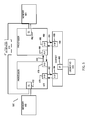
- the hardware state machine 811-817 within each PE 801-807, respectively implements the collective operations and inter-PE communications described herein.
- Each state machine 811-817 may be controlled by a dedicated set of instructions, some examples of which are described below.
- each state machine 811-817 may run asynchronously from instructions executed on the main execution pipeline in PEs 801-807, respectively.
- the collective state 901 of each PE participating in a collective operation is maintained using a relatively small amount of register/buffer storage.
- the amount of register/buffer storage is the same, regardless of how many collectives are in flight and how many cores are in the collective.
- the collective state 901 may include a dynamic collective ID (DCID) selected by software to identify a sequence number for the currently executing collective operation on this PE; an ID of the PE itself 802; an ID of any child PEs 804, 805; and an ID of any parent PE 801 (as indicated in Figure 9 ).
- DCID dynamic collective ID
- each of the IDs comprises an integer value to uniquely identify each PE and each collective in the system.
- the collective state 901 may include the collective operands and data (e.g., collective results). Also illustrated in Figure 9 are functional units 902 for executing the various operations required by the collective (as well as other instructions supported by the PE ISA) and responsively updating the current state 901 within the register/buffer storage.
- the instructions and state machine described herein can easily be implemented as an addition to nearly any type of instruction set architecture (ISA), core, and memory system (e.g., cachable, uncachable, coherent, multiprogrammed, user-level, supervisor level, etc). No access or interference with the memory semantics of the system is required.
- the interconnect fabric simply needs to be used to uniquely identify all PEs (e.g., 'cores') on the network and pass messages directly from state machine to state machine on the PEs.
- the arrangement of PEs shown in Figures 8-9 represent the logical interconnections between PEs, not physical interconnections.
- the logical interconnections are programmed into each PE via instructions used to establish a virtual collective interconnect (VCI) between the PEs.
- VCI virtual collective interconnect
- the physical interconnections may be implemented using any type of fabric or bus structure for connecting multiple cores, processors, or other types of PEs (e.g., such as those discussed with respect to Figures 4-6 ). Although there is no dependence on any particular interconnect topology for this invention to properly function, person skilled in the art will understand that certain mappings of the tree topology to PEs will optimize the behavior.
- a reduction performs operations on all values spread across all PEs and an all-reduction effectively performs a reduction where all PEs get a copy of the result.
- a broadcast causes data to be broadcast from one PE to all or a subset of PEs.
- a barrier forces all PEs to reach a common point in execution before all can proceed (i.e., forces a rendezvous between PEs).
- a Parallel prefix is a broad class of instructions in which a cumulative sum of a sequence of numbers x 0 , x 1 , x 2 , ...
- Setup arranges cores in a binary tree in one embodiment, but someone skilled in the art could generalize to a variety of alternate interconnection patterns. For each PE, the IDs of 0, 1, or 2 neighboring "child” PEs and 0 or 1 "parent" PEs. Setup also specifies the collective operation to be performed (e.g., reduction, broadcast, barrier, allreduce, parallel prefix, etc), and the computational operation (add, or, xor, mul, etc). Software issues setup for any change in topology or operation of the collective. In addition, setup chooses the dynamic collective ID (DCID), a unique ID shared by all PEs in a collective. Every PE in a given collective calls setup with the same DCID. Although in this embodiment the setup instruction specifies the operation, it is feasible for those skilled in the art to define similar protocols where the operation is specified in other instructions in the protocol.
- DCID dynamic collective ID
- Initiate indicates that the local PE is ready to begin participating in the collective operation and supplies its input (if any) for the operation. For some operations, only one PE executes initiate (broadcast); for others (reduction, barrier, and allreduce), software must initiate on all PEs in the collective.
- Wait may be called by software when it needs to know if a collective operation (specified by a particular DCID) has completed. Wait retrieves any result or partial result from the operation and writes it to a processor register. All PEs must wait to complete a collective operation.
- Next is used to allow a sequence of collective operations to be pipelined on the same topology and operation.
- it causes the hardware to generate a new DCID based on the unique DCID given in setup (e.g., incrementing to a next value).
- a subsequent initiate instruction uses the DCID returned by next.
- Teardown is called to deallocate/deactivate the collective operation when software is done with a collective.
- the virtual collective interconnect is stored in a distributed manner in which each PE holds the parent and child PE numbers that globally comprise a binary tree. No one PE needs to know the entire extent of the collective - only the IDs of their direct parent and child PEs (if any).
- the "root" PE e.g., PE 801 in Figure 8
- the collection of all the parent and child PE ID fields in the collective state 901 define the virtual interconnect topology and membership in each collective.
- asynchronous, pipelined collective operation is achieved by the operation of the state machines 811-817.
- the state machines 811-817 may be implemented in dedicated hardware in each PE and execute the collective operations in the background (i.e., as the PEs process other instructions unrelated to the collective).
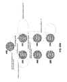
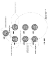
- Figures 10A-C illustrate state transition diagrams specifying the operation of state machines for different roles in the VCI hierarchy.
- Figure 10A illustrates the operation of a root PE having children but no parents
- Figure 10B illustrates the operation of an internal PE having both children and parents
- Figure 10C illustrates the operation of an edge PE having a parent but no children.
- a state machine 811-817 is in a "Done" state 1000 when no collective operation is outstanding.
- a setup instruction forces a core's state machine to a state where it waits for operand(s) for an upcoming reduction operation 1001 or broadcast operation 1002.
- the state machine sends its own local reduction result 1003 to its parent ("c2p” stands for "child-to-parent” in Figures 10A-C) or sends a broadcast result 1004 to it children.
- the results are sent to the next receiver higher or lower in the VCI hierarchy depending on the type of operation (i.e., broadcast or c2p).
- the PE then waits for the child-to-parent acknowledgement 1005 or broadcast acknowledgement 1006 for all packets.
- the state machine may first perform a reduction operation followed by a broadcast operation.
- Figure 10A illustrates the operation of a root PE, which has no parents, the send child-to-parent response 1003 and wait for child-to-parent acknowledgement 1005 states are not utilized. Rather, only broadcast states 1004 and 1006 are used to broadcast results to children and wait for acknowledgements, respectively.
- Figure 10B illustrates the operation of an internal node, which has both parents and children
- the send child-to-parent response 1003 and wait for child-to-parent acknowledgement 1005 states are utilized (for communicating collective results up the hierarchy).
- the broadcast states 1004 and 1006 are used to broadcast results to the children PEs and wait for acknowledgements, respectively.
- Figure 10C illustrates the operation of an edge node, which a parent but no children
- the send child-to-parent response 1003 and wait for child-to-parent acknowledgement 1005 states are utilized (for communicating collective results up the hierarchy).
- the broadcast states 1004 and 1006 are not needed to broadcast results to children PEs and wait for acknowledgements, respectively (i.e., because the PE has no children).
- the software protocol requires software to complete sequences, which ensures the finite hardware buffering is never oversubscribed.
- the initiate operation tells hardware that the PE is ready to participate in the specified DCID/collective and provides the PE's contribution to the computation.
- the wait operation tells the hardware to wait until this PE's state machine has completed its role in the specified collective. Once wait finishes, the PE is free to start another collective using the same setup even though the prior collective may still be in flight elsewhere on the machine, thereby efficiently utilizing the PEs processing resources.
- the setup operation identifies collectives and their topology (as previously discussed) and the teardown operation deallocates resources when a PE is done participating in the collective.
- the teardown operation deallocates resources when a PE is done participating in the collective.
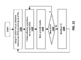
- FIG. 11 A method in accordance with one embodiment of the invention is illustrated in Figure 11 .
- the method may be implemented on an architecture such as those described above.
- the underlying principles of the invention are not limited to any particular processor architecture.
- a setup operation is performed to configured the PE within a particular virtual collective interconnect comprised of a set of PEs.
- the PE may be configured to fit within a particular location of a binary tree structure such as that shown in Figure 8 . To do so, the PE will be informed of parent PEs (if any) and child PEs (if any), and a current DCID all provided by software.
- the setup operation specifies the collective operation to be performed (e.g., reduction, broadcast, barrier, allreduce, parallel prefix, etc), and the computational operation (add, or, xor, mul, etc).
- the initiate operation indicates that the local PE is ready to begin participating in the collective operation and supplies its input (if any) for the operation. For some operations, only one PE executes initiate (broadcast); for others (reduction, barrier, and allreduce), software must initiate on all PEs in the collective.
- the wait operation causes the PE to retrieve any result or partial result from the operation and write it to a processor register. As mentioned, all PEs must wait to complete a collective operation.
- software decides whether to use the same topology to pipeline a sequence of collective operations of the same topology and operation. If so, hardware generates a new DCID based on the original DCID (e.g., incrementing to a next value) and a new initiate operation uses the new DCID. If not, then at 1105 software can initiate a teardown to deallocate/deactivate the collective operation. As indicated, the process may then return to 1101 as a new setup is performed on the PE (i.e., allocating the PE to a new DCID).
- the embodiments described herein do not require global communications to start a new collective.
- the unique DCID provided by software is used by hardware to detect when a PE is trying to pass a value to a PE that has not yet joined the collective.
- the combined hardware and software protocols ensure no global synchronizations are needed, even when moving a PE among collectives with different members, topologies, or operations. If a PE's state machine receives a collective message for something other than its current DCID, it may reject the message with a "retry-later" sent to the message source.
- One embodiment which never uses "retry" messages would require larger PE-local buffering or global synchronizations between changes in collective topology.
- software after a teardown and while setting up a new partition, software must choose a DCID that will not conflict with any DCID's that may be in use on any of the PEs in the new collective.
- a PE may exit a collective and perform independent work.
- hardware uses a default identity value. For example, if data being fed to the collective is distributed asymmetrically across PEs, then a PE may "run out" of data before the collective across all PEs has finished.
- the out-of-data PE could execute SW to explicitly provide identity values, or it can provide an identity value to be used at each step, and then the PE can exit the collective and go perform other work.
- identity values For example, in Figure 8 , once PE 807 exits the collective, there is no need to explicitly forward the identity, instead the parent PE 804 can use the identity value directly
- a PE forwards values without waiting for all senders to provide values.
- missing senders may contribute a default identity value.
- the described embodiments avoid setup barriers as well as requiring the PEs to explicitly manage them during execution. Collectives are implemented with an asynchronous state machine. As such, the local PE initiates communication, then can go do other work without needing to manage communication. Software does not interact further until it requests the result. Software can choose to 'wait' or 'poll' to see if a collective is complete. This transforms the requirement for a global barrier/synchronization in to system that uses a data-flow "wavefront" of results that ripple across the machine - never requiring a complete synchronization to be surfaced.
- Collections of PEs may be setup, torn-down, modified, and collective operations commenced without any global communications before or after and without any software-based buffer space allocation or preparation. Avoiding global communication is beneficial because setup overheads (e.g., global barriers) have limited the usability of prior systems due to such inefficiencies. Software may need to ensure a well-defined sequence of collectives to avoid circular dependences, but this requirement is no different from that required to write a parallel program on any other machine.
- Collectives may also be executed across arbitrary subsets of PEs at the software's discretion. There are no limits to which cores can or cannot participate. Subset flexibility is atypical of hardware-based collective solutions. The approach described herein depends only on an interconnect that can route collective messages between PEs, and PEs that are uniquely identifiable by software.
- a series of collectives can be pipelined across the collection of PEs. Given resources of just a single collective in hardware, the embodiments described herein allow collectives to be pipelined (wavefront) across the system without increasing the amount of storage or buffering required.
- the above features may use only a constant amount of hardware buffering state per PE, regardless of how many collectives are in flight and how many PEs are in the collective. This means collectives on large machines can be implemented using a small number of internal registers and without further memory or cache. Furthermore, the described embodiments need no software buffering of message state other than the unique IDs of collectives in progress. Consequently, these embodiments can operate independently of memory architecture, cache coherence, and physical delivery of messages.
- the collective hardware may support an optional "default child value” mode which allows asymmetric computations to complete on a PE, with hardware providing an identity value for the collective rather than requiring software to "feed" identities.
- the collective hardware may support an optional continuous streaming mode that allows continual update of results fed with a stream of inputs for reductions plus identities, rather than waiting for all leaf nodes as in the "discrete" mode.
- Embodiments of the invention may include various steps, which have been described above.
- the steps may be embodied in machine-executable instructions which may be used to cause a general-purpose or special-purpose processor to perform the steps.
- these steps may be performed by specific hardware components that contain hardwired logic for performing the steps, or by any combination of programmed computer components and custom hardware components.
- instructions may refer to specific configurations of hardware such as application specific integrated circuits (ASICs) configured to perform certain operations or having a predetermined functionality or software instructions stored in memory embodied in a non-transitory computer readable medium.
- ASICs application specific integrated circuits
- the techniques shown in the figures can be implemented using code and data stored and executed on one or more electronic devices (e.g., an end station, a network element, etc.).
- Such electronic devices store and communicate (internally and/or with other electronic devices over a network) code and data using computer machine-readable media, such as non-transitory computer machine-readable storage media (e.g., magnetic disks; optical disks; random access memory; read only memory; flash memory devices; phase-change memory) and transitory computer machine-readable communication media (e.g., electrical, optical, acoustical or other form of propagated signals - such as carrier waves, infrared signals, digital signals, etc.).
- non-transitory computer machine-readable storage media e.g., magnetic disks; optical disks; random access memory; read only memory; flash memory devices; phase-change memory
- transitory computer machine-readable communication media e.g., electrical, optical, acoustical or other form of propagated signals - such as carrier waves, infrared signals, digital signals, etc.
- such electronic devices typically include a set of one or more processors coupled to one or more other components, such as one or more storage devices (non-transitory machine-readable storage media), user input/output devices (e.g., a keyboard, a touchscreen, and/or a display), and network connections.
- the coupling of the set of processors and other components is typically through one or more busses and bridges (also termed as bus controllers).
- the storage device and signals carrying the network traffic respectively represent one or more machine-readable storage media and machine-readable communication media.
- the storage device of a given electronic device typically stores code and/or data for execution on the set of one or more processors of that electronic device.
Landscapes
- Engineering & Computer Science (AREA)
- Theoretical Computer Science (AREA)
- Physics & Mathematics (AREA)
- General Engineering & Computer Science (AREA)
- Computer Hardware Design (AREA)
- General Physics & Mathematics (AREA)
- Software Systems (AREA)
- Mathematical Physics (AREA)
- Advance Control (AREA)
- Communication Control (AREA)
- Multi Processors (AREA)
- Computer And Data Communications (AREA)
Applications Claiming Priority (1)
| Application Number | Priority Date | Filing Date | Title |
|---|---|---|---|
| US14/040,676 US9477628B2 (en) | 2013-09-28 | 2013-09-28 | Collective communications apparatus and method for parallel systems |
Publications (2)
| Publication Number | Publication Date |
|---|---|
| EP2860643A2 true EP2860643A2 (de) | 2015-04-15 |
| EP2860643A3 EP2860643A3 (de) | 2016-05-04 |
Family
ID=51627207
Family Applications (1)
| Application Number | Title | Priority Date | Filing Date |
|---|---|---|---|
| EP14186688.9A Ceased EP2860643A3 (de) | 2013-09-28 | 2014-09-26 | Kollektive Kommunikationsvorrichtung und Verfahren für parallele Systeme |
Country Status (2)
| Country | Link |
|---|---|
| US (1) | US9477628B2 (de) |
| EP (1) | EP2860643A3 (de) |
Families Citing this family (3)
| Publication number | Priority date | Publication date | Assignee | Title |
|---|---|---|---|---|
| US10360163B2 (en) | 2016-10-27 | 2019-07-23 | Google Llc | Exploiting input data sparsity in neural network compute units |
| CN108536121B (zh) * | 2018-03-16 | 2021-04-23 | 深圳市道通科技股份有限公司 | 逻辑通道的建立方法、装置和交通工具通信接口vci |
| US11061742B2 (en) * | 2018-06-27 | 2021-07-13 | Intel Corporation | System, apparatus and method for barrier synchronization in a multi-threaded processor |
Citations (1)
| Publication number | Priority date | Publication date | Assignee | Title |
|---|---|---|---|---|
| US20110296137A1 (en) * | 2010-05-28 | 2011-12-01 | International Business Machines Corporation | Performing A Deterministic Reduction Operation In A Parallel Computer |
Family Cites Families (10)
| Publication number | Priority date | Publication date | Assignee | Title |
|---|---|---|---|---|
| US5418915A (en) * | 1990-08-08 | 1995-05-23 | Sumitomo Metal Industries, Ltd. | Arithmetic unit for SIMD type parallel computer |
| JP2770603B2 (ja) * | 1991-03-14 | 1998-07-02 | 三菱電機株式会社 | 並列計算機 |
| US6839728B2 (en) * | 1998-10-09 | 2005-01-04 | Pts Corporation | Efficient complex multiplication and fast fourier transform (FFT) implementation on the manarray architecture |
| WO2006020298A2 (en) | 2004-07-19 | 2006-02-23 | Blumrich Matthias A | Collective network for computer structures |
| US7159059B2 (en) * | 2002-03-01 | 2007-01-02 | Mcneil Donald H | Ultra-modular processor in lattice topology |
| EP1658563B1 (de) * | 2003-08-28 | 2013-06-05 | MIPS Technologies, Inc. | Vorrichtung und verfahren zur einleitung gleichzeitiger anweisungsströme in einem mehrthread-mikroprozessor |
| US8140826B2 (en) | 2007-05-29 | 2012-03-20 | International Business Machines Corporation | Executing a gather operation on a parallel computer |
| JP5241384B2 (ja) * | 2008-08-29 | 2013-07-17 | ルネサスエレクトロニクス株式会社 | 分散共有メモリ型マルチプロセッサ及びデータ処理方法 |
| RU2580036C2 (ru) * | 2013-06-28 | 2016-04-10 | Закрытое акционерное общество "Лаборатория Касперского" | Система и способ создания гибкой свертки для обнаружения вредоносных программ |
| US10360050B2 (en) * | 2014-01-17 | 2019-07-23 | International Business Machines Corporation | Simulation of high performance computing (HPC) application environment using virtual nodes |
-
2013
- 2013-09-28 US US14/040,676 patent/US9477628B2/en active Active
-
2014
- 2014-09-26 EP EP14186688.9A patent/EP2860643A3/de not_active Ceased
Patent Citations (1)
| Publication number | Priority date | Publication date | Assignee | Title |
|---|---|---|---|---|
| US20110296137A1 (en) * | 2010-05-28 | 2011-12-01 | International Business Machines Corporation | Performing A Deterministic Reduction Operation In A Parallel Computer |
Also Published As
| Publication number | Publication date |
|---|---|
| US20150095542A1 (en) | 2015-04-02 |
| US9477628B2 (en) | 2016-10-25 |
| EP2860643A3 (de) | 2016-05-04 |
Similar Documents
| Publication | Publication Date | Title |
|---|---|---|
| CN109213523B (zh) | 具有存储器系统性能、功率减小和原子支持特征的可配置空间加速器的处理器、方法和系统 | |
| CN109215728B (zh) | 用于分布式存储器危险检测和错误恢复的存储器电路和方法 | |
| CN108268278B (zh) | 具有可配置空间加速器的处理器、方法和系统 | |
| CN107408036B (zh) | 用户级分叉与结合处理器、方法、系统和指令 | |
| JP6051458B2 (ja) | 複数のハッシュ動作を効率的に実行する方法および装置 | |
| JP6340097B2 (ja) | リードマスク及びライトマスクにより制御されるベクトル移動命令 | |
| CN104603748B (zh) | 具有多个核、共享的核扩展逻辑及共享的核扩展利用指令的处理器 | |
| JP6373425B2 (ja) | 複数のビットを左にシフトし、複数の1を複数の下位ビットにプルインするための命令 | |
| JP6143872B2 (ja) | 装置、方法、およびシステム | |
| CN108885586B (zh) | 用于以有保证的完成将数据取出到所指示的高速缓存层级的处理器、方法、系统和指令 | |
| US10700968B2 (en) | Optimized function assignment in a multi-core processor | |
| US10678541B2 (en) | Processors having fully-connected interconnects shared by vector conflict instructions and permute instructions | |
| US10127043B2 (en) | Implementing conflict-free instructions for concurrent operation on a processor | |
| CN109597684B (zh) | 处理器中的动态性能偏置 | |
| US11360809B2 (en) | Multithreaded processor core with hardware-assisted task scheduling | |
| CN110647404A (zh) | 用于多线程处理器中的屏障同步的系统、设备和方法 | |
| CN111752616A (zh) | 用于符号存储地址生成的系统、装置和方法 | |
| TWI751125B (zh) | 用以監控位址衝突的計數器 | |
| CN107003944A (zh) | 跨分布式存储器的指针追踪 | |
| US9477628B2 (en) | Collective communications apparatus and method for parallel systems | |
| JP4444305B2 (ja) | 半導体装置 | |
| CN112148106A (zh) | 用于处理器的混合预留站的系统、装置和方法 | |
| US20180349137A1 (en) | Reconfiguring a processor without a system reset | |
| US11176278B2 (en) | Efficient rotate adder for implementing cryptographic basic operations | |
| US12613696B2 (en) | System, apparatus and method for throttling fusion of micro-operations in a processor |
Legal Events
| Date | Code | Title | Description |
|---|---|---|---|
| PUAI | Public reference made under article 153(3) epc to a published international application that has entered the european phase |
Free format text: ORIGINAL CODE: 0009012 |
|
| 17P | Request for examination filed |
Effective date: 20140926 |
|
| AK | Designated contracting states |
Kind code of ref document: A2 Designated state(s): AL AT BE BG CH CY CZ DE DK EE ES FI FR GB GR HR HU IE IS IT LI LT LU LV MC MK MT NL NO PL PT RO RS SE SI SK SM TR |
|
| AX | Request for extension of the european patent |
Extension state: BA ME |
|
| PUAL | Search report despatched |
Free format text: ORIGINAL CODE: 0009013 |
|
| RIC1 | Information provided on ipc code assigned before grant |
Ipc: G06F 9/52 20060101ALI20160318BHEP Ipc: G06F 13/40 20060101ALI20160318BHEP Ipc: G06F 15/173 20060101AFI20160318BHEP |
|
| AK | Designated contracting states |
Kind code of ref document: A3 Designated state(s): AL AT BE BG CH CY CZ DE DK EE ES FI FR GB GR HR HU IE IS IT LI LT LU LV MC MK MT NL NO PL PT RO RS SE SI SK SM TR |
|
| AX | Request for extension of the european patent |
Extension state: BA ME |
|
| STAA | Information on the status of an ep patent application or granted ep patent |
Free format text: STATUS: EXAMINATION IS IN PROGRESS |
|
| 17Q | First examination report despatched |
Effective date: 20191029 |
|
| STAA | Information on the status of an ep patent application or granted ep patent |
Free format text: STATUS: THE APPLICATION HAS BEEN REFUSED |
|
| 18R | Application refused |
Effective date: 20210315 |